Embed Size (px)
Citation preview

Supplementary information
10 nm scale nanopatterning on flexible substrates by secondary sputtering phenomenon and their applications in high performance, flexible and transparent conducting films
Sungwoo Jang, Hwan-Jin Jeon, Cheng Jin An, Ming Liang Jin and Hee-Tae Jung*
Experimental details
Fabrication of a grating structure on a PDMS substrate: To fabricate a grating structure on a PDMS substrate, PDMS is replicated from a silicon master pre-patterned with a depth of 400 nm by using photolithography. The silicon master is placed in a Petri dish with a few drops of chlorotrimethylsilane, which converts the surface of the silicon master from hydrophilic to hydrophobic in order to prevent the adhesion of PDMS to the silicon master. A liquid mixture of 4g of PDMS (Sylgard 184 base: curing agent = 10:1 weight ratio, Dow Corning) is added to the Petri dish, and bubbles are removed in a desiccator. The petri dish is then placed in an 80ºC oven and cured for 2 h. The PDMS grating structure is removed from the silicon master by peeling.
Fabrication of a PUA grating structure on a PET substrate:To fabricate the PUA grating structure on a PET substrate, PUA (MINS-311RM, Minuta Technology Co, Ltd) is dropped onto the silicon master. It is then cured by exposure to UV (λ=365 nm) for 30 s through a PET film. After UV curing, the PET substrate with a PUA grating structure is removed from the master by peeling.
Fabrication of a metallic pattern on a flexible substrate with SSP:The target material is deposited on the flexible substrate with a thickness of 30 nm by using an electron beam evaporator. The 10 nm scale nanopattern is then prepared through the SSP deposition of the ejected target material on the sidewalls of the grating structure during an Ar+ ion milling process with a beam power of 500eV.
Fabrication of OPVc on the flexible substrate with SSP:To test the flexible transparent electrode in a flexible organic solar cell, a Au line pattern with a spacing of 500 nm on the sidewalls of a PUA grating structure on a PET film was converted into a hole transfer electrode (Fig. S4). After cleaning this electrode in the sonicator, a PEDOT:PSS layer (Baytron PVP AI4083, HC Stack) was deposited on the sample by spin casting at 2500 rpm for 40 s. After annealing, the active layer consisting of P3HT (4002-EE grade, Rieke Metals) and PC60BM (Nano-C (99.5%)) dissolved in chlorobenzene was deposited by spin casting and dried for 120 min in a N2 glove box. The Al electrode layer was then loaded by using a thermal evaporator. The performance of this flexible organic solar cell was assessed by using a solar simulator (Newport 66902, calibrated with a BS-520BK diode). The power conversion efficiency of the flexible device was found to be 0.65% (Jsc=4.66 mA/cm2, Voc=0.51 mA, fill factor=0.28). These results demonstrate the potential of the SSP approach to the fabrication of flexible organic devices.
Electronic Supplementary Material (ESI) for Journal of Materials Chemistry C.This journal is © The Royal Society of Chemistry 2014

Fig.S1 Fabrication of a metal line pattern on the sidewalls of a PUA grating structure on a PET substrate over a large area (3 cm x 4 cm). Fabrication of the silicon master with photolithography (a). Replica molding of the grating structure from the silicon master on the PUA substrate with UV curing (b). After the SSP process, a Au line pattern is formed on the sidewalls of the PUA grating structure on the PET substrate over a large area (c). The SEM image shows that the ultrathin Au line pattern is aligned on the sidewalls of the PUA grating structure (d).
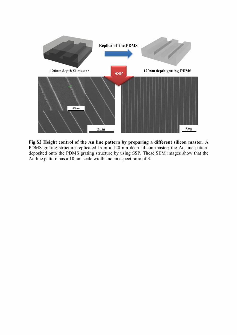
Fig.S2 Height control of the Au line pattern by preparing a different silicon master. A PDMS grating structure replicated from a 120 nm deep silicon master; the Au line pattern deposited onto the PDMS grating structure by using SSP. These SEM images show that the Au line pattern has a 10 nm scale width and an aspect ratio of 3.

Fig.S3 SEM images of Au line patterns after applying strains of 6% and 18%. At a strain of 6%, the Au line pattern on the PDMS substrate is without defect (a). At a strain of 18%, the Au line pattern on the PDMS substrate is broken (b).

Fig.S4 Fabrication of a flexible transparent conducting film with SSP and its performance as a hole transfer electrode in a flexible organic solar cell device. Schematic diagram of the fabrication of the flexible organic solar cell with a Au line patterned electrode with a spacing of 500 nm on the sidewalls of a PUA grating structure on a PET substrate (a). Current density versus bias voltage curve of the flexible organic solar cell (b).