Embed Size (px)
Citation preview
1
SUPPLEMENTARY INFORMATION
Graphene Foam with A Three-Dimensional Interconnected Network and Its High-
Conducting Composites
S1. Characterization of the graphene foam (GF) and GF/PDMS composites
a b c
f e d
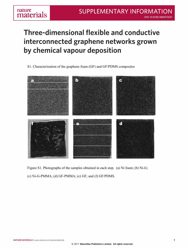
Figure S1. Photographs of the samples obtained in each step. (a) Ni foam; (b) Ni-G;
(c) Ni-G-PMMA; (d) GF-PMMA; (e) GF; and (f) GF/PDMS.
Three-dimensional flexible and conductiveinterconnected graphene networks grownby chemical vapour deposition
SUPPLEMENTARY INFORMATIONdoi: 10.1038/nmaT3001
naTure maTerials | www.nature.com/naturematerials 1
© 2011 Macmillan Publishers Limited. All rights reserved.

2
Figure S2. SEM images of the as-grown graphene films adhering to the surface of a
nickel foam. Ripples and wrinkles of the graphene films are observed.
2 naTure maTerials | www.nature.com/naturematerials
SUPPLEMENTARY INFORMATION doi: 10.1038/nmaT3001
© 2011 Macmillan Publishers Limited. All rights reserved.
3
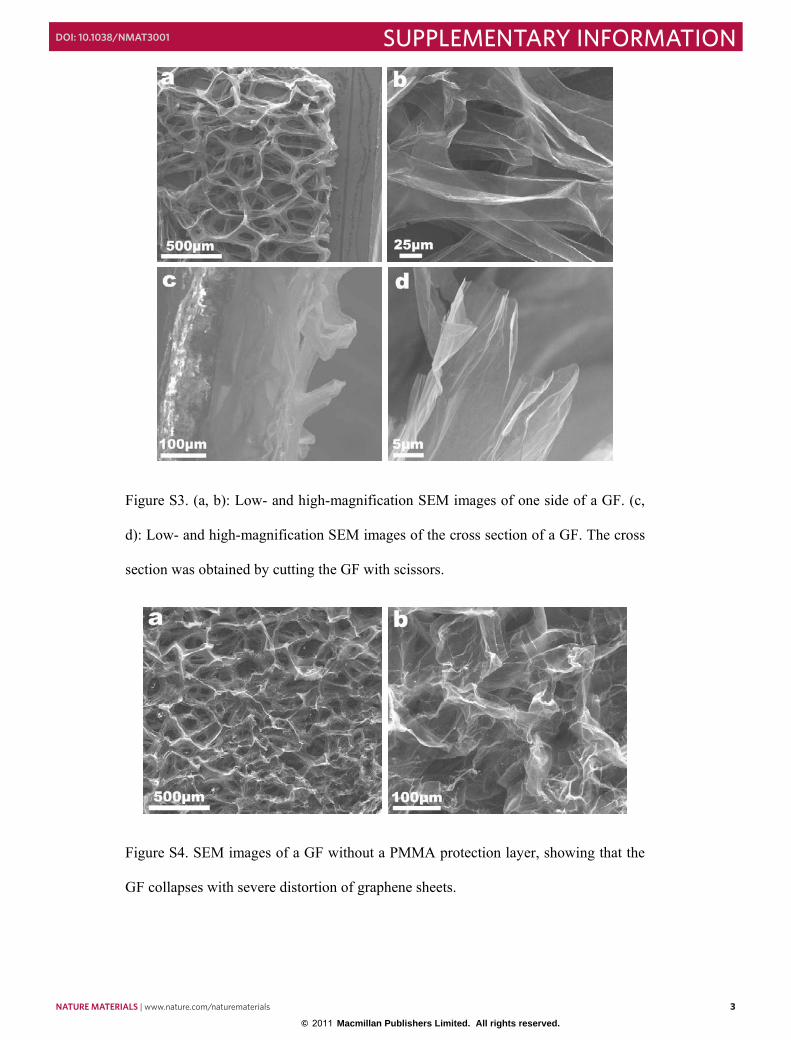
Figure S3. (a, b): Low- and high-magnification SEM images of one side of a GF. (c,
d): Low- and high-magnification SEM images of the cross section of a GF. The cross
section was obtained by cutting the GF with scissors.
Figure S4. SEM images of a GF without a PMMA protection layer, showing that the
GF collapses with severe distortion of graphene sheets.
naTure maTerials | www.nature.com/naturematerials 3
SUPPLEMENTARY INFORMATIONdoi: 10.1038/nmaT3001
© 2011 Macmillan Publishers Limited. All rights reserved.

4
3 4 5 6 7 8 9 102
3
4
5
6
Spec
ific
surf
ace
area
(m2 /g
)
Den
sity
(mg/
cm3 )
Average number of layers
200
400
600
800
3 4 5 6 7 8 9 100
100
200
300
400
500
600
Mas
s (m
g)
Thin
knes
s ( μ
m)
Average number of layers
0.2
0.4
0.6
0.8
1.0
1.2
1.4
ba
Figure S5. (a) Thickness and mass of GFs as a function of the average number of
graphene layers. (b) The density and specific surface area of GFs as a function of the
average number of graphene layers.
Figure S6. SEM images of (a, c) graphene films on nickel foams and (b, d) the
resultant GFs. The nickel foams used in a and c have 95 and 115 pores per inch,
respectively. All the scale bars are 250 μm.
4 naTure maTerials | www.nature.com/naturematerials
SUPPLEMENTARY INFORMATION doi: 10.1038/nmaT3001
© 2011 Macmillan Publishers Limited. All rights reserved.
5
0.2 0.4 0.6 0.8 1.0 1.2 1.423456789
10
Ave
rage
num
ber o
f lay
ers
CH4 concentration (vol%)
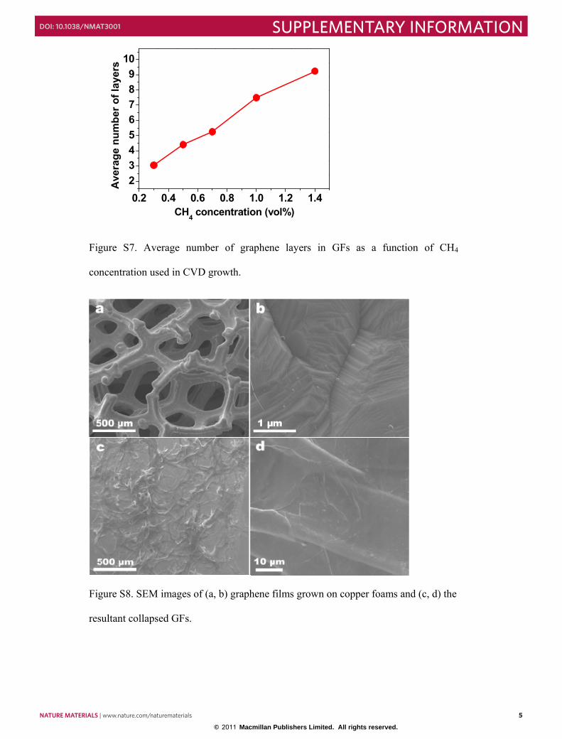
Figure S7. Average number of graphene layers in GFs as a function of CH4
concentration used in CVD growth.
Figure S8. SEM images of (a, b) graphene films grown on copper foams and (c, d) the
resultant collapsed GFs.
naTure maTerials | www.nature.com/naturematerials 5
SUPPLEMENTARY INFORMATIONdoi: 10.1038/nmaT3001
© 2011 Macmillan Publishers Limited. All rights reserved.
6
a b
c d
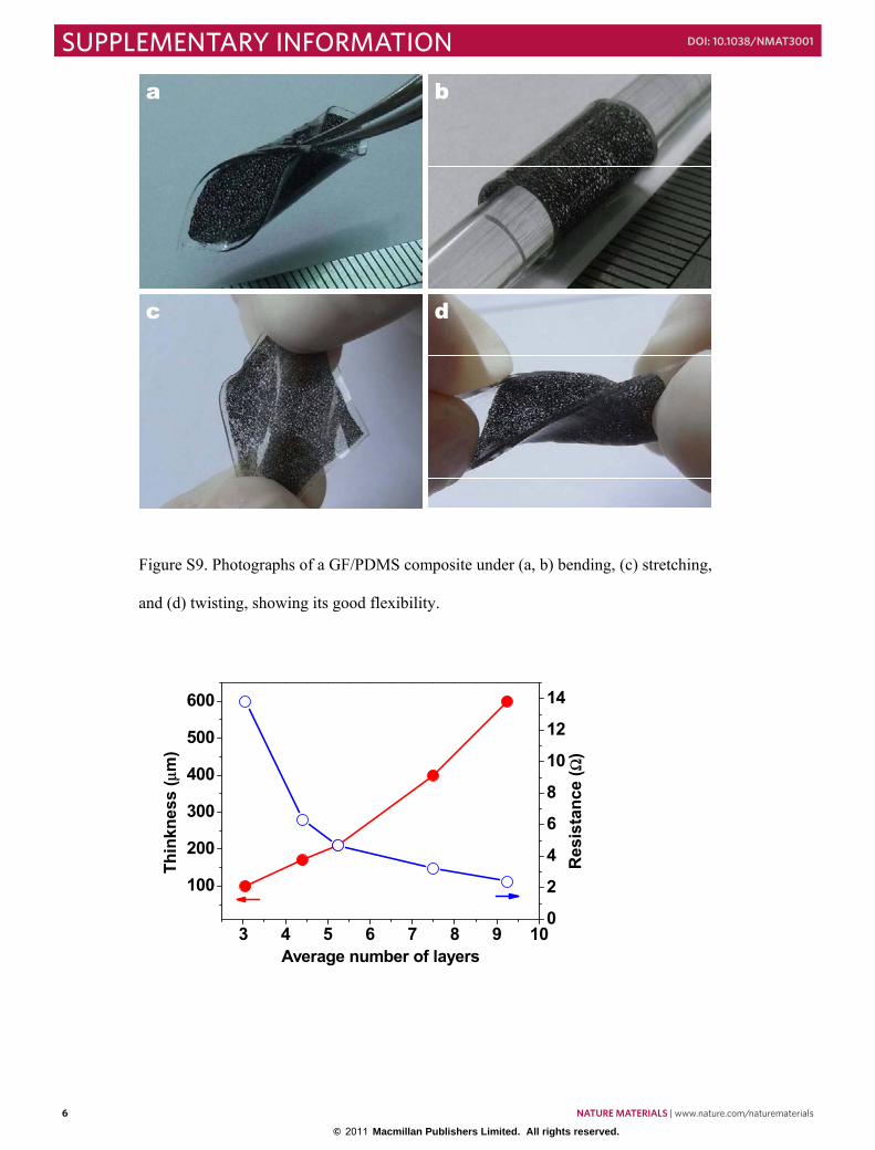
Figure S9. Photographs of a GF/PDMS composite under (a, b) bending, (c) stretching,
and (d) twisting, showing its good flexibility.
3 4 5 6 7 8 9 10
100
200
300
400
500
600
Res
ista
nce
(Ω)
Thin
knes
s ( μ
m)
Average number of layers
0
2
4
6
8
10
12
14
6 naTure maTerials | www.nature.com/naturematerials
SUPPLEMENTARY INFORMATION doi: 10.1038/nmaT3001
© 2011 Macmillan Publishers Limited. All rights reserved.
7
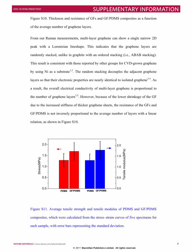
Figure S10. Thickness and resistance of GFs and GF/PDMS composites as a function
of the average number of graphene layers.
From our Raman measurements, multi-layer graphene can show a single narrow 2D
peak with a Lorentzian lineshape. This indicates that the graphene layers are
randomly stacked, unlike in graphite with an ordered stacking (i.e., ABAB stacking).
This result is consistent with those reported by other groups for CVD-grown graphene
by using Ni as a substrate1,2. The random stacking decouples the adjacent graphene
layers so that their electronic properties are nearly identical to isolated graphene3-5. As
a result, the overall electrical conductivity of multi-layer graphene is proportional to
the number of graphene layers3,5. However, because of the lower shrinkage of the GF
due to the increased stiffness of thicker graphene sheets, the resistance of the GFs and
GF/PDMS is not inversely proportional to the average number of layers with a linear
relation, as shown in Figure S10.
0.0
0.5
1.0
1.5
2.0
Tens
ile m
odul
us(M
Pa)
Stre
ss(M
Pa)
PDMS GF/PDMS PDMS GF/PDMS0.0
0.5
1.0
1.5
2.0
Figure S11. Average tensile strength and tensile modulus of PDMS and GF/PDMS
composites, which were calculated from the stress–strain curves of five specimens for
each sample, with error bars representing the standard deviation.
naTure maTerials | www.nature.com/naturematerials 7
SUPPLEMENTARY INFORMATIONdoi: 10.1038/nmaT3001
© 2011 Macmillan Publishers Limited. All rights reserved.

8
Figure S12. Photographs of GF/PDMS (a−c and a´−c´) and Ni foam/PDMS (d−f and
d´−f´) composites before, under and after mechanical deformation. It can be found
that the GF/PDMS composites have good elasticity and can recover to their initial
form after releasing strain, while the Ni foam/PDMS composites cannot recover but
remain in bent or stretched forms.
a b
fed
c
Bending Initial Release
8 naTure maTerials | www.nature.com/naturematerials
SUPPLEMENTARY INFORMATION doi: 10.1038/nmaT3001
© 2011 Macmillan Publishers Limited. All rights reserved.
9
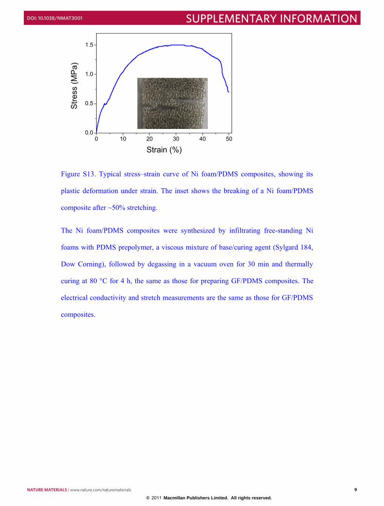
Figure S13. Typical stress–strain curve of Ni foam/PDMS composites, showing its
plastic deformation under strain. The inset shows the breaking of a Ni foam/PDMS
composite after ~50% stretching.
The Ni foam/PDMS composites were synthesized by infiltrating free-standing Ni
foams with PDMS prepolymer, a viscous mixture of base/curing agent (Sylgard 184,
Dow Corning), followed by degassing in a vacuum oven for 30 min and thermally
curing at 80 °C for 4 h, the same as those for preparing GF/PDMS composites. The
electrical conductivity and stretch measurements are the same as those for GF/PDMS
composites.
0 10 20 30 40 500.0
0.5
1.0
1.5
Stre
ss (M
Pa)
Strain (%)
naTure maTerials | www.nature.com/naturematerials 9
SUPPLEMENTARY INFORMATIONdoi: 10.1038/nmaT3001
© 2011 Macmillan Publishers Limited. All rights reserved.

10
1 2 3 4 5 6 7 8 9 10 11 120
10
20
30
√
√
10%
30%
max strain zero strain
ΔR/R
0(%)
Stretching cycles
50%
√
Figure S14. Electrical resistance change of GF/PDMS composites after 10, 30, and
50% stretching and then releasing for each cycle. It can be seen that an irreversible
resistance change of the composites occurs in the first few cycles. Moreover, the
irreversible resistance increase is larger for a larger maximum tensile strain, indicating
that it can be intrinsically attributed to the partial breaking or cracking of the GF
network. The cycle when the resistance change becomes stable has been marked. The
number of cycles needed for GF/PDMS conductors becoming stable also depends on
the degree of mechanical deformation. Under larger maximum deformation, more
cycles are needed for the GF/PDMS conductors to become stable.
10 naTure maTerials | www.nature.com/naturematerials
SUPPLEMENTARY INFORMATION doi: 10.1038/nmaT3001
© 2011 Macmillan Publishers Limited. All rights reserved.

11
S2. Comparison of the electrical conductivity of GF/PDMS with CNT based
composites.
Table S1. Typical CNT composites and their electrical conductivity
Conducting
fillers/polymer
Conducting
filler content
Electrical
conductivity Reference
SWNT/polyimide 0.5 vol% 3×10⁻⁷ S/cm Ounaies, Z., et al.6
SWNT/polystyrene 7 wt% 6.89×10⁻² S/cm Ramasubramaniam,
R., et al.7
SWNT/polyimide 0.2 vol% ~1×10⁻⁶ S/cm McLachlan, D. S. et
al.8
SWNT/polystyrene 0.5 wt% ~1×10⁻³ S/cm Grossiord, N et al.9
SWNT/polystyrene 8.5 wt% 1.34×10⁻⁷S/cm Barraza, H.J et al.10
MWNT/PVA 0.54 wt% 1.14×10⁻⁸ S/cm Kilbride, B.E. et al.11
SWNT/polyimide 0.2 vol% 1×10⁻⁷S/cm Park, C. et al.12
SWNT/PMMA 1.3 wt% 1.18×10⁻³S/cm Haggenmueller, R et
al.13
GF/PDMS 0.5 wt%
(0.22 vol%) 10 S/cm Our work
S3. Evaluation of the specific surface area of GFs and their average number of
graphene layers.
Considering that a nickel foam is fully covered by graphene after CVD growth, the
surface area of the GF (SGF) is twice that of the nickel foam template used, which can
be measured by nitrogen gas cryosorption (Micromeritics, ASAP2010M). Therefore,
the specific surface area of GF and its average number of layers (N) of graphene
sheets can be calculated as follows:
naTure maTerials | www.nature.com/naturematerials 11
SUPPLEMENTARY INFORMATIONdoi: 10.1038/nmaT3001
© 2011 Macmillan Publishers Limited. All rights reserved.
12
SGF=2×(SNi×WNi) (1)
S’GF= SGF/WGF (2)
N= SG/S’GF (3)
where SNi and WNi are the specific surface area and weight of the nickel foam template,
respectively; S’GF and WGF are the specific surface area and weight of the GF,
respectively; SG≈2600 m2/g14, corresponds to the theoretical value of the specific
surface area of a monolayer graphene.
References
1. Reina, A. et al. Large area, few-layer graphene films on arbitrary substrates by chemical vapor deposition. Nano Lett. 9, 30-35 (2009).
2. Alfonso Reina, S.T., Xiaoting Jia, Sreekar Bhaviripudi, Mildred S. Dresselhaus, Juergen A. Growth of large-area single- and bi-layer graphene by controlled carbon precipitation on polycrystalline Ni surfaces Nano Res. 2, 509-516 (2009).
3. Bae, S. et al. Roll-to-roll production of 30-inch graphene films for transparent electrodes. Nature Nanotechnol. 5, 574-578 (2010).
4. Hass, J. et al. Why multilayer graphene on 4H-SiC(0001) behaves like a single sheet of graphene. Phys. Rev. Lett. 100, 125504 (2008).
5. Li, X.S. et al. Transfer of large-area graphene films for high-performance transparent conductive electrodes. Nano Lett. 9, 4359-4363 (2009).
6. Ounaies, Z., Park, C., Wise, K.E., Siochi, E.J. & Harrison, J.S. Electrical properties of single wall carbon nanotube reinforced polyimide composites. Compos. Sci. Technol. 63, 1637-1646 (2003).
7. Ramasubramaniam, R., Chen, J. & Liu, H.Y. Homogeneous carbon nanotube/polymer composites for electrical applications. Appl. Phys. Lett. 83, 2928-2930 (2003).
8. McLachlan, D.S. et al. Ac and dc percolative conductivity of single wall carbon nanotube polymer composites. J. Polym. Sci., Part B: Polym. Phys. 43, 3273-3287 (2005).
9. Grossiord, N., Loos, J. & Koning, C.E. Strategies for dispersing carbon nanotubes in highly viscous polymers. J. Mater. Chem. 15, 2349-2352 (2005).
10. Barraza, H.J., Pompeo, F., O'Rear, E.A. & Resasco, D.E. SWNT-filled thermoplastic and elastomeric composites prepared by miniemulsion polymerization. Nano Lett. 2, 797-802 (2002).
11. Kilbride, B.E. et al. Experimental observation of scaling laws for alternating current and direct current conductivity in polymer-carbon nanotube composite thin films. J. Appl. Phys. 92, 4024-4030 (2002).
12 naTure maTerials | www.nature.com/naturematerials
SUPPLEMENTARY INFORMATION doi: 10.1038/nmaT3001
© 2011 Macmillan Publishers Limited. All rights reserved.

13
12. Park, C. et al. Dispersion of single wall carbon nanotubes by in situ polymerization under sonication. Chem. Phys. Lett. 364, 303-308 (2002).
13. Haggenmueller, R., Gommans, H.H., Rinzler, A.G., Fischer, J.E. & Winey, K.I. Aligned single-wall carbon nanotubes in composites by melt processing methods. Chem. Phys. Lett. 330, 219-225 (2000).
14. Stankovich, S. et al. Graphene-based composite materials. Nature 442, 282-286 (2006).
naTure maTerials | www.nature.com/naturematerials 13
SUPPLEMENTARY INFORMATIONdoi: 10.1038/nmaT3001
© 2011 Macmillan Publishers Limited. All rights reserved.