Embed Size (px)
Citation preview
1
Supplementary Note 1. Optic simulation for various optical systems
The ray tracing simulations for each optical system were performed using
commercial software (Zemax, USA). The spherical aberration induces mismatch between the
curved focal plane and the flat image sensor (Supplementary Fig. 1a top), which requires a
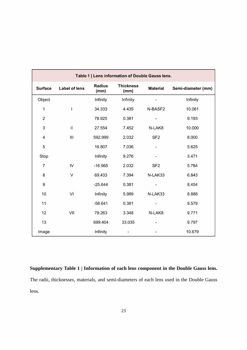
complicated lens configuration in current camera modules. For example, a Double Gauss lens
consists of seven lenses for focusing the image on the planar image sensor, and it needs ~93.2
mm of lateral dimension (Supplementary Fig. 1a bottom). Detailed lens parameters such as
radii, thicknesses, and materials are included in Supplementary Table 1. In addition, achieving
accurate alignment between the individual lenses in the Double Gauss lens increases the
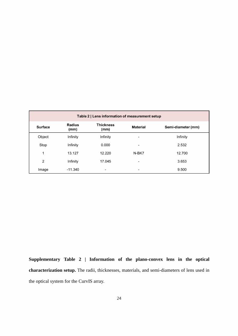
fabrication cost. On the other hand, the CurvIS array using a single plano-convex lens
(Supplementary Table 2) satisfies requirements to achieve the focus on the entire curved focal
plane (Supplementary Fig. 1b). The optic design for this configuration is simple and compact
(~29.3 mm) compared to the multi-lens configurations required for flat image sensors. This
also dramatically reduces the production cost. In these simulations, F-number of 5 was
selected as an aperture stop size. The blue, green, and red lines indicate the rays of light
whose field-of-view are 0º, 14º, and 28º, respectively.
Imaging simulations for each optical system were also performed using the
commercial software. The single plano-convex lens successfully focuses the image on the
CurvIS array without distortion (Supplementary Fig. 2d) similar to the conventional Double
Gauss lens (Supplementary Fig. 2c). On the other hand, an image focused on a flat image
sensor array through a single plano-convex lens is blurred (Supplementary Fig. 2b).
Supplementary Note 2. Theoretical analysis of the soft optoelectronic device based on
mechanics
2
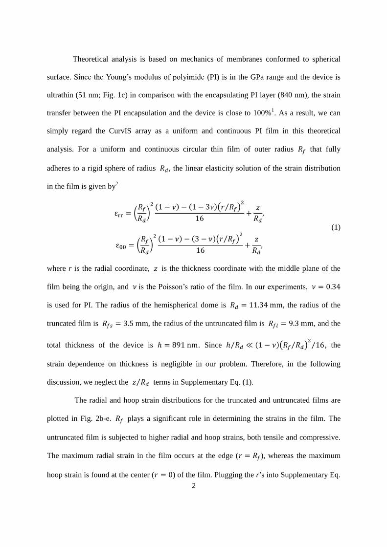
Theoretical analysis is based on mechanics of membranes conformed to spherical
surface. Since the Young’s modulus of polyimide (PI) is in the GPa range and the device is
ultrathin (51 nm; Fig. 1c) in comparison with the encapsulating PI layer (840 nm), the strain
transfer between the PI encapsulation and the device is close to 100%1. As a result, we can
simply regard the CurvIS array as a uniform and continuous PI film in this theoretical
analysis. For a uniform and continuous circular thin film of outer radius 𝑅𝑓 that fully
adheres to a rigid sphere of radius 𝑅𝑑, the linear elasticity solution of the strain distribution
in the film is given by2
εrr = (𝑅𝑓
𝑅𝑑)
2 (1 − 𝜈) − (1 − 3𝜈)(𝑟 𝑅𝑓⁄ )2
16+
𝑧
𝑅𝑑,
εθθ = (𝑅𝑓
𝑅𝑑)
2 (1 − 𝜈) − (3 − 𝜈)(𝑟 𝑅𝑓⁄ )2
16+
𝑧
𝑅𝑑,
(1)
where r is the radial coordinate, 𝑧 is the thickness coordinate with the middle plane of the
film being the origin, and 𝜈 is the Poisson’s ratio of the film. In our experiments, 𝜈 = 0.34
is used for PI. The radius of the hemispherical dome is 𝑅𝑑 = 11.34 mm, the radius of the
truncated film is 𝑅𝑓𝑠 = 3.5 mm, the radius of the untruncated film is 𝑅𝑓𝑙 = 9.3 mm, and the
total thickness of the device is ℎ = 891 nm. Since ℎ 𝑅𝑑⁄ ≪ (1 − 𝜈)(𝑅𝑓 𝑅𝑑⁄ )2
16⁄ , the
strain dependence on thickness is negligible in our problem. Therefore, in the following
discussion, we neglect the 𝑧 𝑅𝑑⁄ terms in Supplementary Eq. (1).
The radial and hoop strain distributions for the truncated and untruncated films are
plotted in Fig. 2b-e. 𝑅𝑓 plays a significant role in determining the strains in the film. The
untruncated film is subjected to higher radial and hoop strains, both tensile and compressive.
The maximum radial strain in the film occurs at the edge (𝑟 = 𝑅𝑓), whereas the maximum
hoop strain is found at the center (𝑟 = 0) of the film. Plugging the r’s into Supplementary Eq.

3
(1), we find that both maximum strains have a quadratic relation with 𝑅𝑓 𝑅𝑑⁄ .
εrr,max = (𝑅𝑓
𝑅𝑑)
2 𝜈
8, εθθ,max = (
𝑅𝑓
𝑅𝑑)
2 (1 − 𝜈)
16 (2)
The maximum radial and hoop strains of truncated and untruncated films are plotted
as functions of 𝑅𝑓 𝑅𝑑⁄ in Fig. 2f. Maximum compressive strains occur at the edge of the
films. The much lower compressive strain in the truncated film can effectively prevent
buckling and folding of the film (Supplementary Fig. 4).
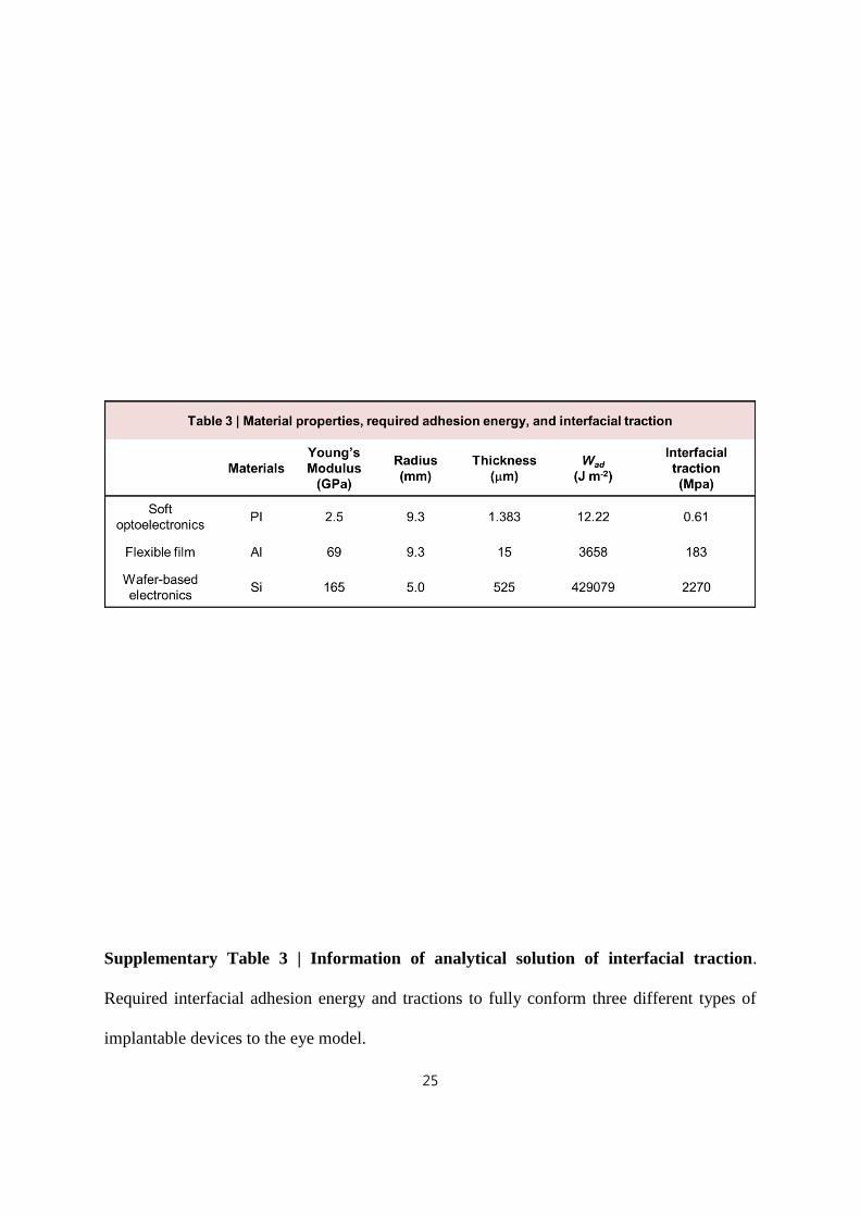
Supplementary Note 3. Analytical solution of interfacial tractions between implantable
devices and the artificial eye model.
For a film of radius 𝑅𝑓 and thickness 𝐻 attached to the eye model of radius 𝑅𝑑,
the interfacial traction deforms the eye model, as evident in Fig. 4c. As we assume the eye
model (i.e., a bilayer hemispherical shell) to be rigid for a quick estimation of the interfacial
traction, the estimated result would be an upper limit and would be more accurate for lower
interfacial traction which induces smaller deformation in the eye model. For full
conformability to the rigid eye model, the adhesion energy of the interface 𝑊𝑎𝑑 must
satisfy2
𝑊𝑎𝑑 ≥ 𝐸𝐻 [1
128(
𝑅𝑓
𝑅𝑑)
4
−𝐻2
12(1 − 𝜈)𝑅𝑑2] (3)
where 𝐸 is the Young’s modulus of the film. Assuming a rectangular traction separation
relation, the interfacial traction 𝜎 can be estimated as
𝜎𝑐 =𝑊𝑎𝑑
𝛿𝑐 (4)
where the maximum separation is assumed to be c = 20 m. In our experiments (Fig. 4c and

4
Supplementary Fig. 13), the radii of the soft optoelectronic device and the flexible film are Rf
= 9.3 mm. The wafer-based electronics is square but we assume it is a circular film of radius
Rf = 5 mm. The material properties, required adhesion energy and interfacial traction of the
three cases are listed in Supplementary Table 3.
5
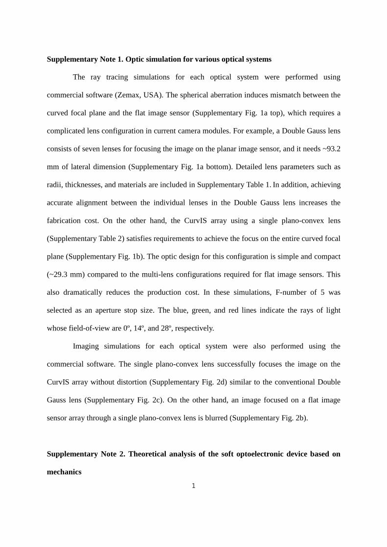
Supplementary Figure 1 | Ray tracing simulation of each optical system. (a) Optical
aberration originated from the mismatch between the curved focal plane and the flat image
sensor (top). Conventional Double Gauss lens to remove optical aberration for the flat image
sensor (bottom). (b) Simplified optics consisting of a single plano-convex lens for the curved
image sensor. (c) Wide field-of-view of the conventional hemispherically curved image
sensor array3.
6
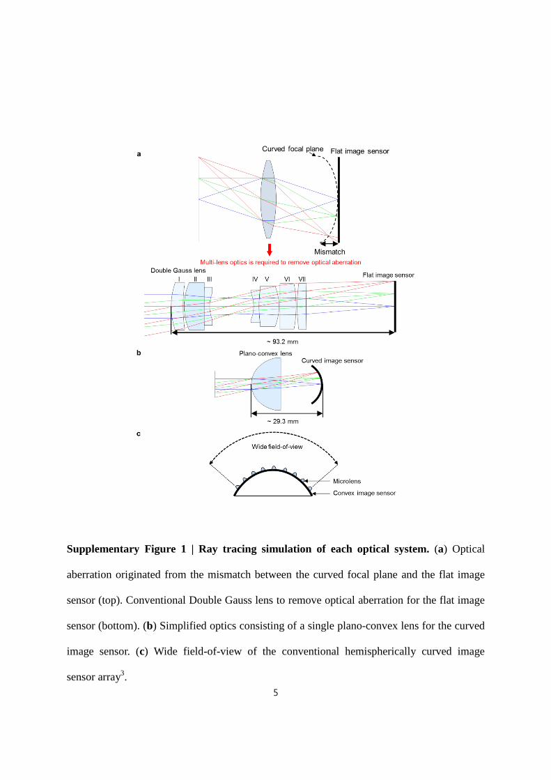
Supplementary Figure 2 | Imaging simulation. (a) Original object. (b-d) images focused
by the three optical systems; single plano-convex lens with the flat image sensor array (b),
Double Gauss lens with the flat image sensor array (c), and single plano-convex lens with the
CurvIS array (d).
7
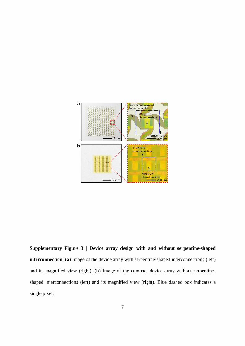
Supplementary Figure 3 | Device array design with and without serpentine-shaped
interconnection. (a) Image of the device array with serpentine-shaped interconnections (left)
and its magnified view (right). (b) Image of the compact device array without serpentine-
shaped interconnections (left) and its magnified view (right). Blue dashed box indicates a
single pixel.
8
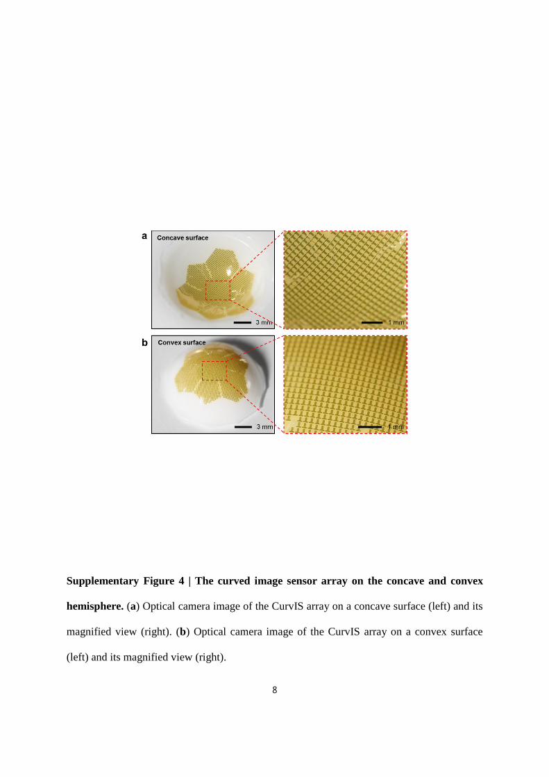
Supplementary Figure 4 | The curved image sensor array on the concave and convex
hemisphere. (a) Optical camera image of the CurvIS array on a concave surface (left) and its
magnified view (right). (b) Optical camera image of the CurvIS array on a convex surface
(left) and its magnified view (right).
9
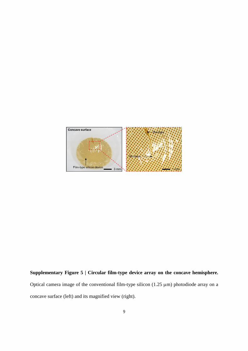
Supplementary Figure 5 | Circular film-type device array on the concave hemisphere.
Optical camera image of the conventional film-type silicon (1.25 m) photodiode array on a
concave surface (left) and its magnified view (right).
10
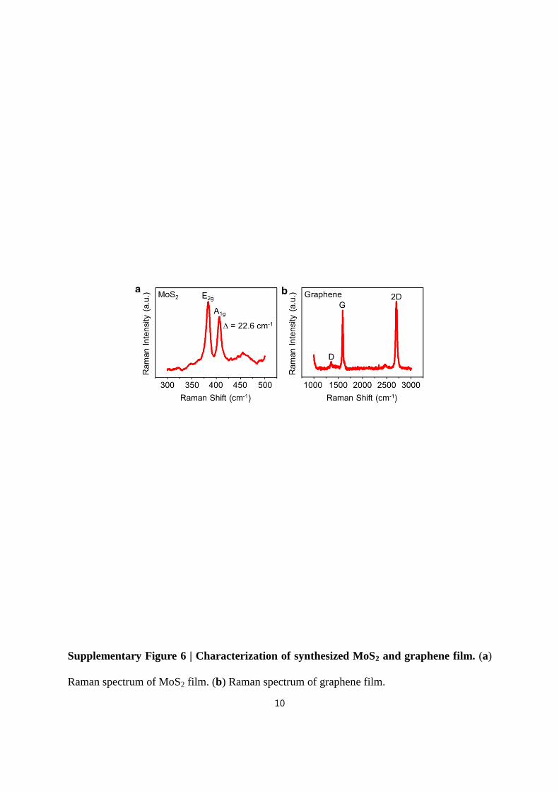
Supplementary Figure 6 | Characterization of synthesized MoS2 and graphene film. (a)
Raman spectrum of MoS2 film. (b) Raman spectrum of graphene film.

11
Supplementary Figure 7 | Fabrication of the phototransistor array based on the MoS2-
graphene heterostructure. (a) Optical microscope images for showing the fabrication
process of a single phototransistor. (b) Scanning electron microscope image of the vertical
structure of the device and the top and bottom PI encapsulations.
12
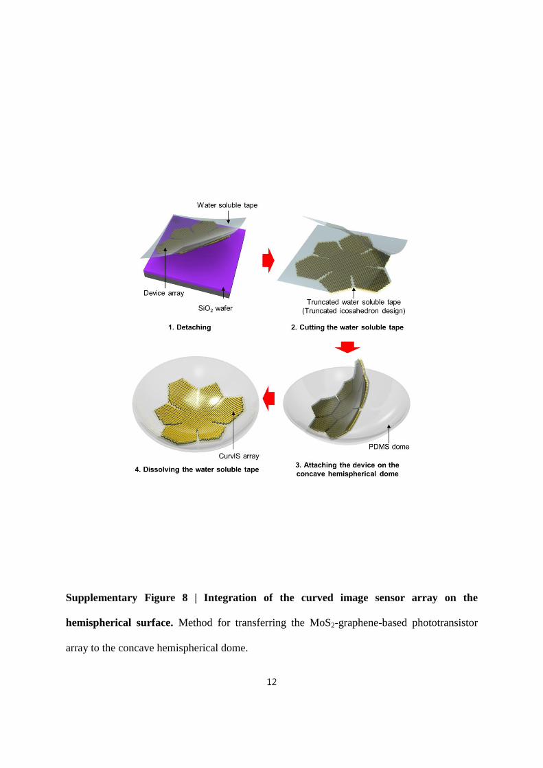
Supplementary Figure 8 | Integration of the curved image sensor array on the
hemispherical surface. Method for transferring the MoS2-graphene-based phototransistor
array to the concave hemispherical dome.
13
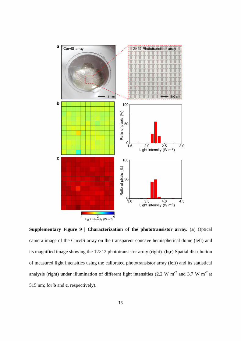
Supplementary Figure 9 | Characterization of the phototransistor array. (a) Optical
camera image of the CurvIS array on the transparent concave hemispherical dome (left) and
its magnified image showing the 12×12 phototransistor array (right). (b,c) Spatial distribution
of measured light intensities using the calibrated phototransistor array (left) and its statistical
analysis (right) under illumination of different light intensities (2.2 W m-2
and 3.7 W m-2
at
515 nm; for b and c, respectively).
14
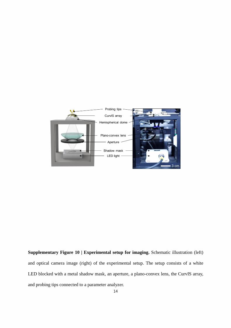
Supplementary Figure 10 | Experimental setup for imaging. Schematic illustration (left)
and optical camera image (right) of the experimental setup. The setup consists of a white
LED blocked with a metal shadow mask, an aperture, a plano-convex lens, the CurvIS array,
and probing tips connected to a parameter analyzer.
15
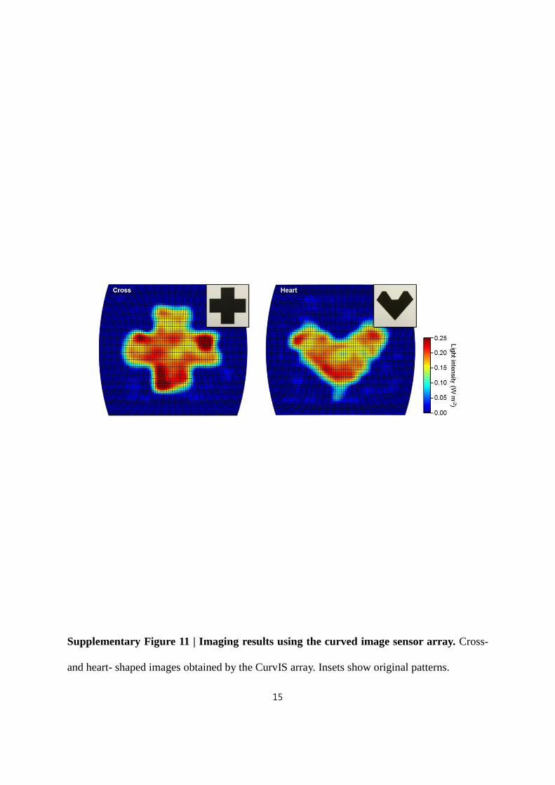
Supplementary Figure 11 | Imaging results using the curved image sensor array. Cross-
and heart- shaped images obtained by the CurvIS array. Insets show original patterns.
16
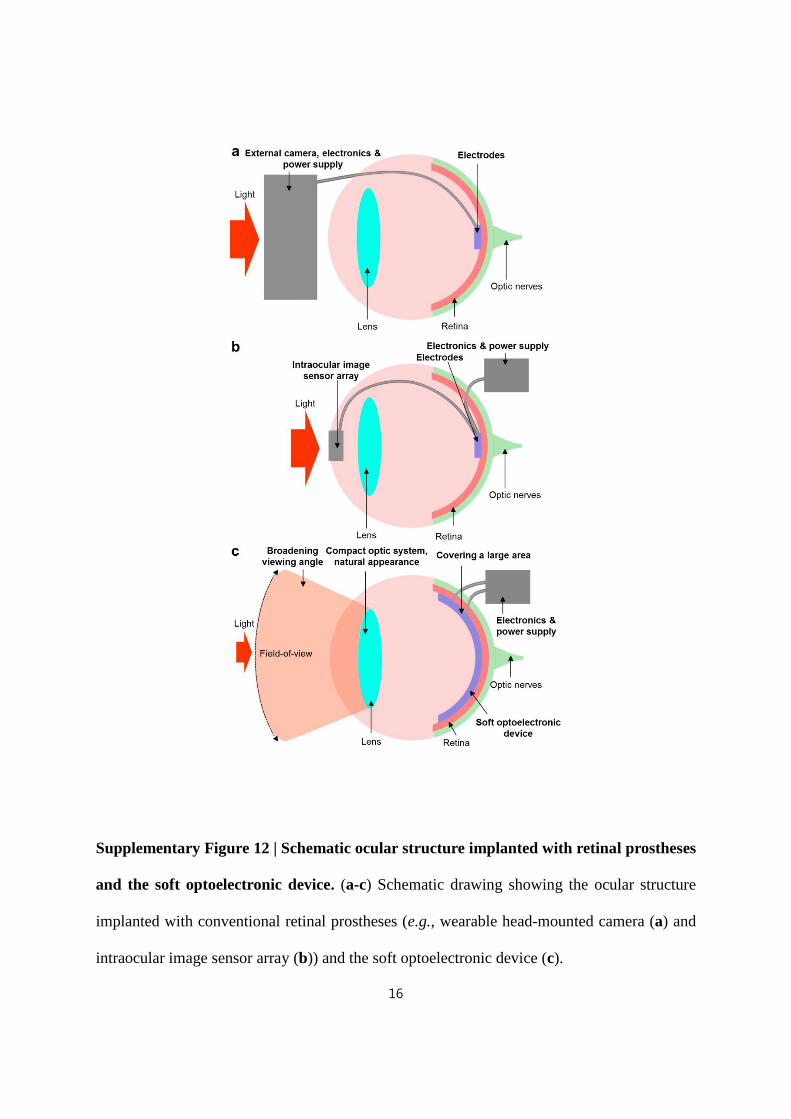
Supplementary Figure 12 | Schematic ocular structure implanted with retinal prostheses
and the soft optoelectronic device. (a-c) Schematic drawing showing the ocular structure
implanted with conventional retinal prostheses (e.g., wearable head-mounted camera (a) and
intraocular image sensor array (b)) and the soft optoelectronic device (c).

17
Supplementary Figure 13 | Eye model for analyzing the retinal deformation. (a)
Schematic illustration of the double-layered eye model that mimics retina (20 kPa)4 and
sclera (1.84 MPa)5 in human eye. (b) Optical camera image of the eye model attached with
the soft optoelectronic device.
18
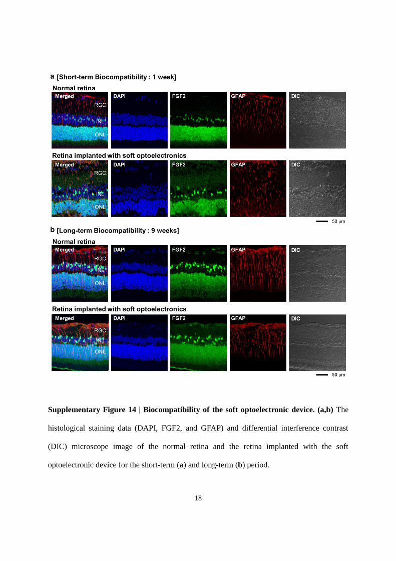
Supplementary Figure 14 | Biocompatibility of the soft optoelectronic device. (a,b) The
histological staining data (DAPI, FGF2, and GFAP) and differential interference contrast
(DIC) microscope image of the normal retina and the retina implanted with the soft
optoelectronic device for the short-term (a) and long-term (b) period.
19
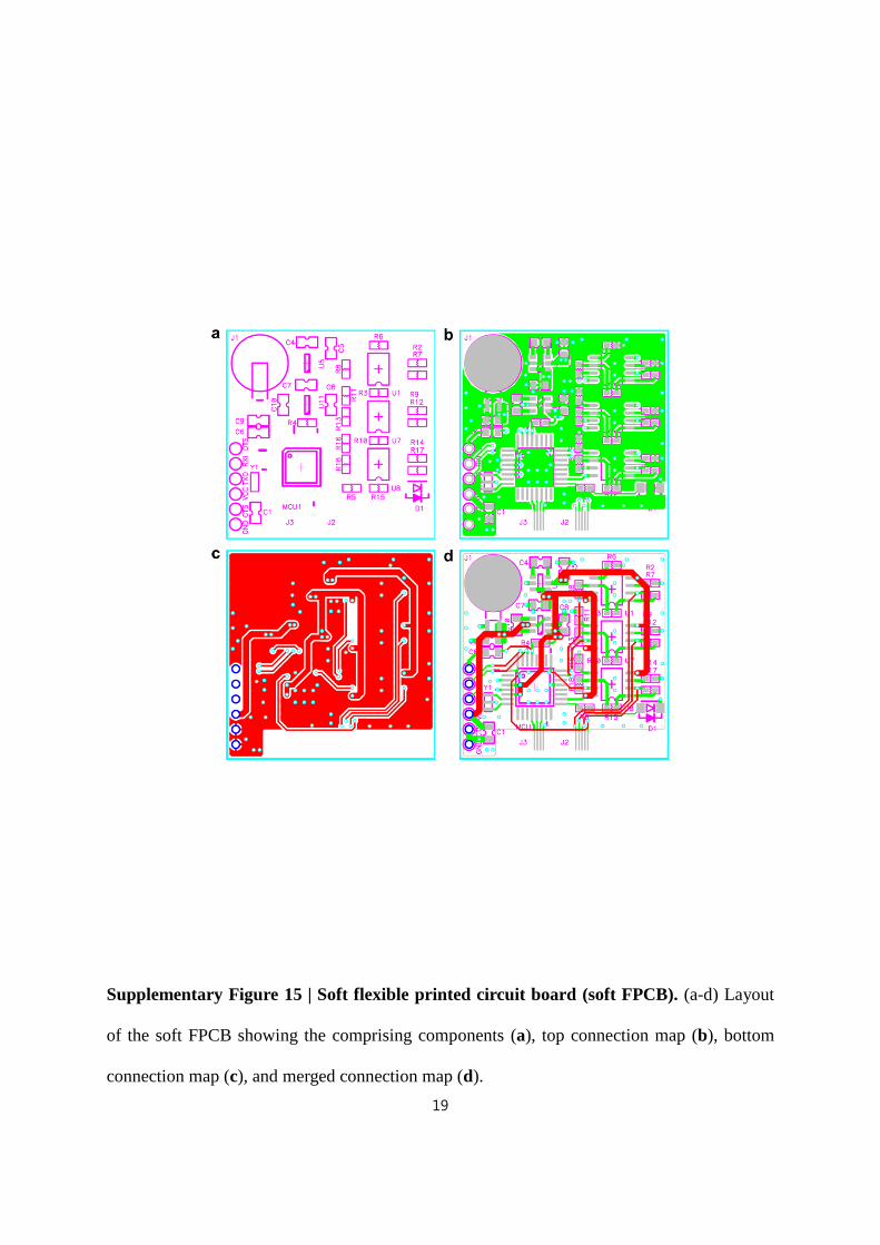
Supplementary Figure 15 | Soft flexible printed circuit board (soft FPCB). (a-d) Layout
of the soft FPCB showing the comprising components (a), top connection map (b), bottom
connection map (c), and merged connection map (d).
20
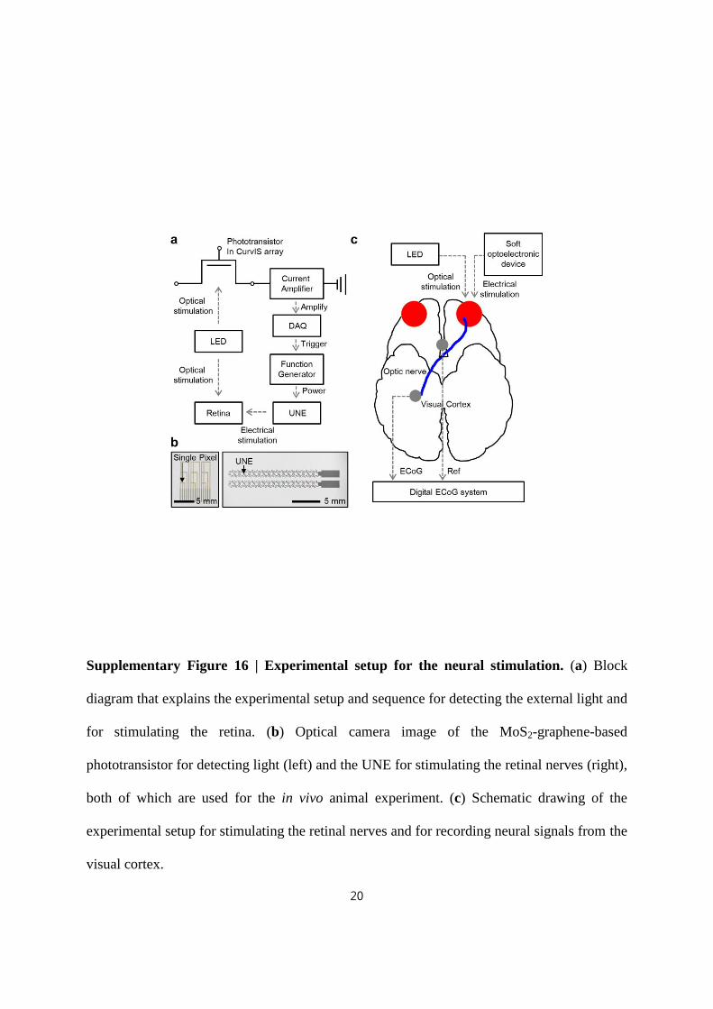
Supplementary Figure 16 | Experimental setup for the neural stimulation. (a) Block
diagram that explains the experimental setup and sequence for detecting the external light and
for stimulating the retina. (b) Optical camera image of the MoS2-graphene-based
phototransistor for detecting light (left) and the UNE for stimulating the retinal nerves (right),
both of which are used for the in vivo animal experiment. (c) Schematic drawing of the
experimental setup for stimulating the retinal nerves and for recording neural signals from the
visual cortex.
21
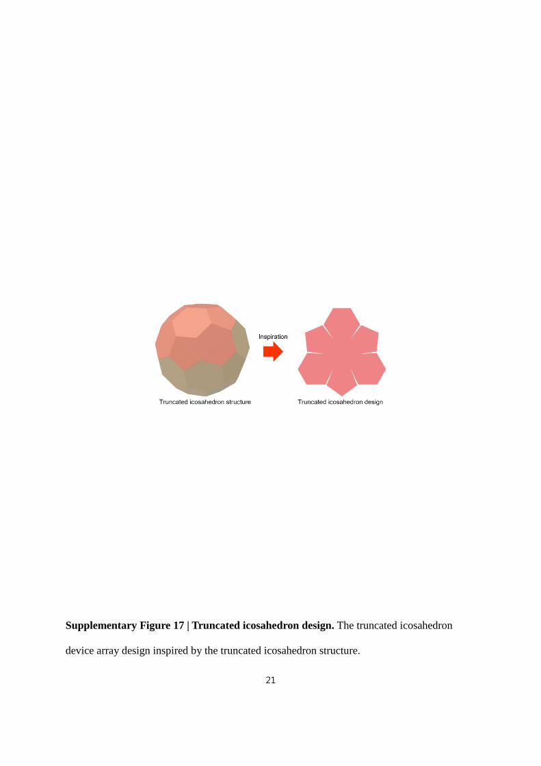
Supplementary Figure 17 | Truncated icosahedron design. The truncated icosahedron
device array design inspired by the truncated icosahedron structure.
22
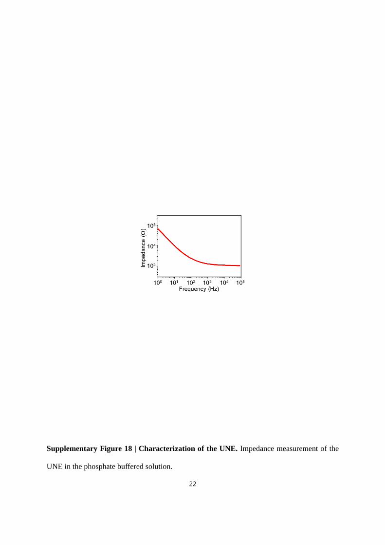
Supplementary Figure 18 | Characterization of the UNE. Impedance measurement of the
UNE in the phosphate buffered solution.
23
Supplementary Table 1 | Information of each lens component in the Double Gauss lens.
The radii, thicknesses, materials, and semi-diameters of each lens used in the Double Gauss
lens.
24
Supplementary Table 2 | Information of the plano-convex lens in the optical
characterization setup. The radii, thicknesses, materials, and semi-diameters of lens used in
the optical system for the CurvIS array.
25
Supplementary Table 3 | Information of analytical solution of interfacial traction.
Required interfacial adhesion energy and tractions to fully conform three different types of
implantable devices to the eye model.
26
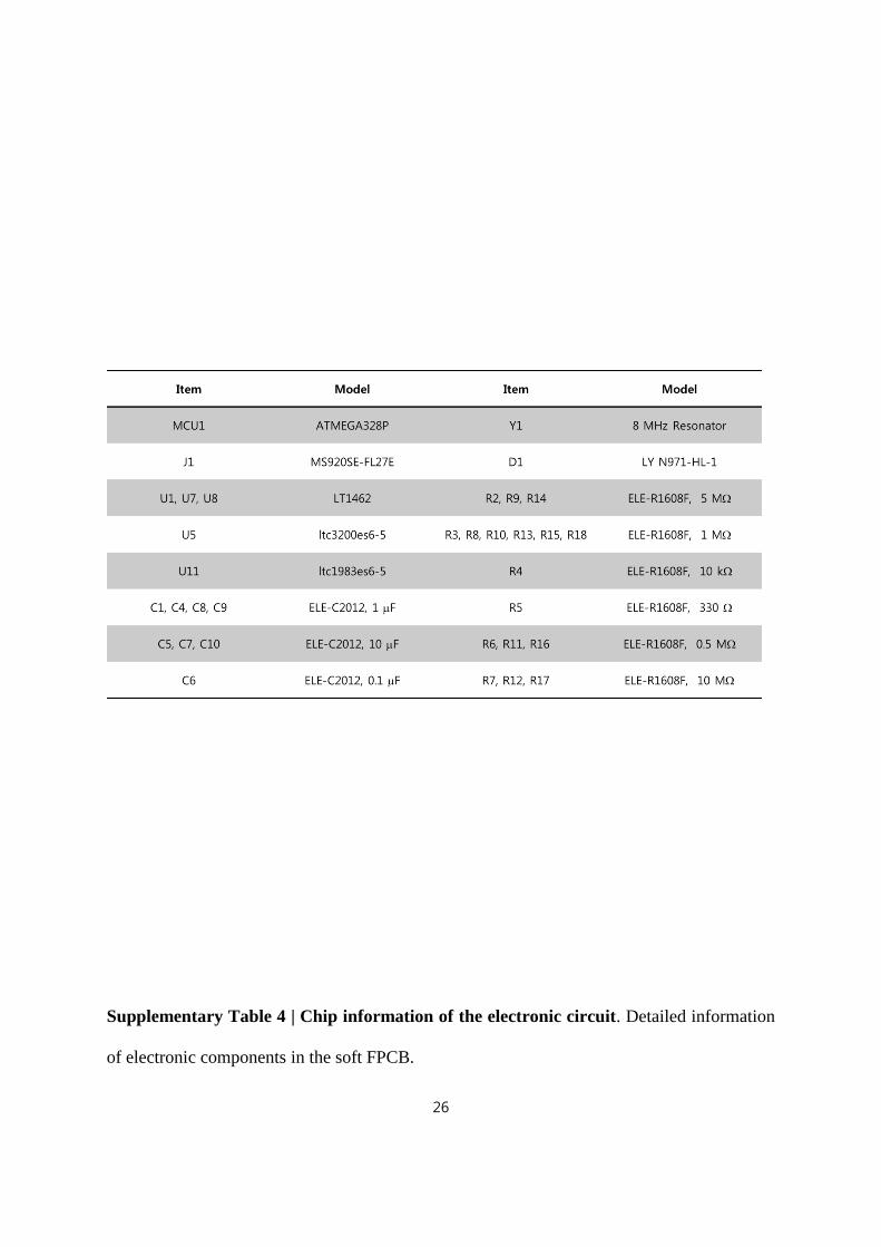
Supplementary Table 4 | Chip information of the electronic circuit. Detailed information
of electronic components in the soft FPCB.

27
Supplementary References
1. Yang, S. & Lu, N. Gauge factor and stretchability of silicon-on-polymer strain gauges,
Sensors 13, 8577–8594 (2013).
2. Majidi, C. & Fearing, R. S. Adhesion of an elastic plate to a sphere. Proc. R. Soc. A 464,
1309–1317 (2008).
3. Song, Y. M. et al. Digital cameras with designs inspired by the arthropod eye. Nature 497,
95–99 (2013).
4. Jones, I. L., Warner, M. & Stevens, J. D. Mathematical modelling of the elastic properties
of retina: a determination of Young’s modulus. Eye 6, 556–559 (1992).
5. Ko, M. W. L. Effect of corneal, scleral and lamina cribrosa elasticity, and intraocular
pressure on optic nerve damages. JSM Ophthalmol. 3, 1024 (2015).