Embed Size (px)
Citation preview

Gold Nanorods
Surface Assembly and Plasmonic Properties in Strongly Coupled Segmented Gold Nanorods
Maneesh K. Gupta , Tobias König , Rachel Near , Dhriti Nepal , Lawrence F. Drummy , Sushmita Biswas , Swati Naik , Richard A. Vaia , Mostafa A. El-Sayed , and Vladimir V. Tsukruk *
© 2013 Wiley-VCH Verlag Gmb
DOI: 10.1002/smll.201300248
An assembly strategy is reported such that segmented nanorods fabricated through template-assisted methods can be robustly transferred and tethered to a pre-functionalized substrate with excellent uniformity over large surface areas. After embedding the rods, sacrifi cial nickel segments were selectively etched leaving behind strongly coupled segmented gold nanorods with gaps between rods below 40 nm and as small as 2 nm. Hyper-spectral imaging is utilized to measure Rayleigh scattering spectra from individual and coupled nanorod elements in contrast to common bulk measurements. This approach discerns the effects of not only changing segment and gap size but also the presence of characteristic defects on the plasmonic coupling between closely spaced nanorods. Polarized hyper-spectral measurements are conducted to provide direct observation of the anisotropic plasmonic resonance modes in individual and coupled nanorods, which are close to those predicted by computer simulations for nanorods with ideal shapes. Some common deviations from ideal shape such as non-fl at facets and asymmetric tails are demonstrated to result in the appearance of characteristic plasmon resonances, which have not been considered before. The large-scale assembly of coupled noble nanostructures with fi ne control over geometry and high uniformity provides means to strongly tune the scattering, absorption, and near-fi eld plasmonic properties through the geometric arrangement of precisely controlled nanorod segments.
M. K. Gupta, Dr. T. Konig, S. Naik, Prof. V. V. TsukrukSchool of Materials Science and Engineering Georgia Institute of Technology Atlanta GA 30332, USA E-mail: [email protected]
R. Near, Prof. M. A. El-SayedSchool of Chemistry and Biochemistry Georgia Institute of Technology Atlanta, GA 30332, USA
Dr. D. Nepal, Dr. L. F. Drummy, Dr. S. Biswas, Dr. R. A. VaiaMaterials and Manufacturing Directorate Air Force Research Laboratory Wright-Patterson AFB, OH 45433, USA
small 2013, 9, No. 17, 2979–2990
1. Introduction
The coupling of localized surface plasmon resonances (LSPR)
in noble metal nanostructures provides a versatile approach
to precisely tailor optical properties such as absorption, scat-
tering, and near-fi eld enhancement. [ 1–9 ] Recent studies have
shown that nanoparticle assemblies with strongly coupled
plasmons are of tremendous interest for a broad range of
important applications including optoelectronics, photo-
voltaics, biological/chemical sensors, and nanophotonics to
name a few. [ 10–17 ] However, the ability to precisely fabri-
cate large numbers of monodisperse assemblies remains a
signifi cant bottleneck for their effective utilization in many
emerging applications.
2979H & Co. KGaA, Weinheim wileyonlinelibrary.com

M. K. Gupta et al.
298
full papers
Top-down fabrication techniques such as electron-beamlithography have been used with tremendous success to fab-
ricate user-defi ned nanoparticle arrays. These tools have been
widely used to study fundamental aspects of LSPR coupling
interactions such as the ‘plasmon ruler equation’, and have
more recently provided examples of Fano resonances and
negative-index metamaterials in plasmonic systems. [ 18–27 ]
While these tools provide users with unparalleled control
over the assembly geometry, they result in polycrystalline
nanoparticles, which can have signifi cant losses, and are
largely restricted by the high-cost and intricacy of the fab-
rication process. [ 28 ] On the other hand, bottom-up assembly
of nanostructures, while offering advantages of single crystal
structures, atomically smooth surfaces, low cost, and easy
scalability, has typically been limited by the rigorous design
requirements of chemical or biomolecular linkers needed
to achieve diverse geometries and spacings along with the
comparatively higher polydispersity among assemblies. [ 29–38 ]
However, recent studies have demonstrated tremendous
progress in the efforts to generalize assembly of complex
structures both in solution and on solid substrates. [ 39–47 ]
Template based strategies have been shown to provide
an intermediate approach for precisely fabricating plasmonic
nanostructures with a high-degree of control and in large
quantities relative to conventional top-down methods. [ 48–52 ]
In particular, porous anodic alumina (PAA) templates
have proven to be extremely versatile for the fabrication
of metal nanorods using both electro-less and electrodepo-
sition methods. [ 53–60 ] Based on these techniques a number
of studies have demonstrated the ability to fabricate linear
arrays of nanorods with controlled diameter, length, and gap
between rod segments by sequential deposition of metals fol-
lowed by selective etching of sacrifi cial metal segments. [ 61–68 ]
The strong near-fi eld enhancement in the gaps between adja-
cent segments in these array structures have been thoroughly
investigated especially for use in optical antenna and sur-
face enhanced Raman scattering (SERS) applications. [ 69–72 ]
These template-assisted arrays have tremendous potential
for a wide range of applications including photovoltaics, elec-
tronics, and biological/chemical sensing owing to the ability
precisely tailor the geometric and compositional structure of
the array along with the high-throughput and relatively low-
cost of fabrication.
Current strategies for preserving the inter-rod gaps in tem-
plate fabricated arrays are based on vapor phase deposition
of backing layers followed by re-dispersion and then etching
of sacrifi cial metal segments. [ 73 ] This approach serves excep-
tionally well for applications, such as in situ biosensing, where
dispersible nanorod arrays are desired. [ 74 ] However, there
remain numerous applications, including substrate-based sen-
sors, photovoltaics, and optoelectronics, in which nanorod
arrays are desired on fi xed substrates. For these applications,
high-throughput and effi cient techniques to assemble these
multi-segmented nanorods directly on substrates while pre-
serving the local array structure are critical to realize the
broader potential of these template-based arrays. Addition-
ally, optical techniques capable of addressing and resolving
individual array elements must be utilized to characterize the
infl uence of structural, compositional, ambient dielectric, and
0 www.small-journal.com © 2013 Wiley-VCH V
substrate interaction factors on the far-fi eld optical proper-
ties. Currently measurement of far-fi eld optical properties in
template-assisted arrays has been limited to ensemble meas-
urements of solutions of randomly oriented nanorods with
unpolarized light.
In this report we develop materials processing strategies
so that micron-long, multi-segmented nanorods with diam-
eters as small as 50 nm, nanorod segments ranging from 70 to
150 nm in length, and gaps between nanorods ranging from
40 to 2 nm can be robustly transferred to a pre-functional-
ized substrate without compromising the original linear array
structure. Hyper-spectral imaging was utilized to measure
Rayleigh scattering spectra from the individual and coupled
nanorod elements in contrast to common bulk measurements.
This approach allowed us to discern the effects of not only
changing segment and gap size but also the presence of char-
acteristic defects on the plasmonic coupling between closely
spaced nanorods. Polarized hyper-spectral measurements
were conducted to provide direct observation of the aniso-
tropic plasmonic resonance modes in individual and coupled
nanorods which are close to those predicted by computer
simulations for nanorods with ideal shapes. The polarized
measurements also provided a means to identify scattering
modes that may arise from anomalous structural features.
Some common deviations from ideal shape such as non-fl at
facets and asymmetric tails were demonstrated to result in
appearance of characteristic plasmon resonances which have
not been considered before. Simulations of ideal and rough-
ened nanorods allowed for identifi cation of fi ne structural
features that may cause the new scattering modes observed
in polarized measurements of individual nanostructures.
2. Results and Discussion
2.1. Assembly of Segmented Nanorods on Surfaces
The linear nanorod arrays analyzed in this report were fab-
ricated by sequential electrodeposition of silver, gold, and
nickel metals into porous alumina templates with pore diam-
eters of 50 nm ( Figure 1 a–c) using a thin sputter coated gold
fi lm as the working electrode (see Experimental Section).
In order to facilitate high-throughput and monodisperse
synthesis of the segmented nanorods, large area templates
( > 10 cm 2 ) with highly uniform pore diameters were fabri-
cated and used.
A major challenge of template-based fabrication is that
upon dissolution of the template a signifi cant number of the
nanorods can become ‘bundled’ irreversibly into aggregates,
signifi cantly reducing the throughput of the synthesis. This
problem is particularly severe with small diameter nanorods
( < 100 nm diameter) that have higher surface energy and a
greater propensity to aggregate. To overcome these issues,
we dissolved the alumina template in a 1M NaOH solution
containing 10 mg/mL of polystyrene sulfonate (PSS) to act
as a capping layer for the rods. [ 75 , 76 ] Furthermore, the alu-
mina was dissolved with the working electrode intact, and the
rods were functionalized with PSS as an array. This approach
kept the nanorods well separated allowing the PSS to diffuse
erlag GmbH & Co. KGaA, Weinheim small 2013, 9, No. 17, 2979–2990
Strongly Coupled Segmented Gold Nanorods
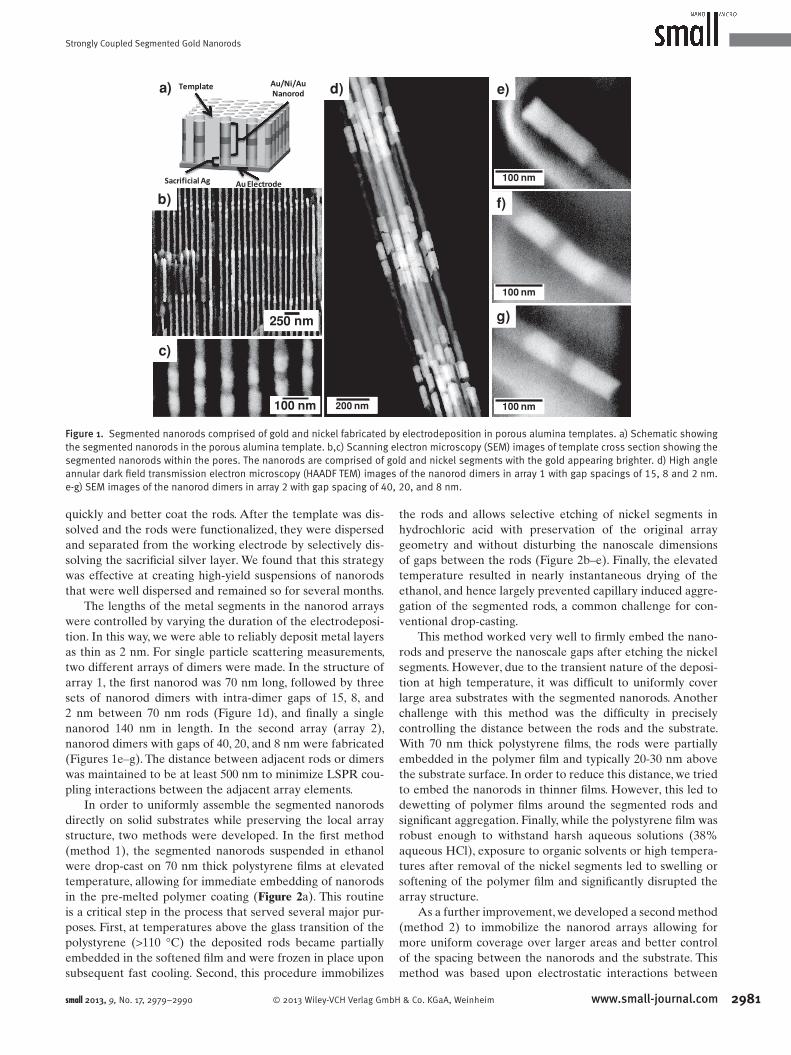
Figure 1 . Segmented nanorods comprised of gold and nickel fabricated by electrodeposition in porous alumina templates. a) Schematic showing the segmented nanorods in the porous alumina template. b,c) Scanning electron microscopy (SEM) images of template cross section showing the segmented nanorods within the pores. The nanorods are comprised of gold and nickel segments with the gold appearing brighter. d) High angle annular dark fi eld transmission electron microscopy (HAADF TEM) images of the nanorod dimers in array 1 with gap spacings of 15, 8 and 2 nm. e-g) SEM images of the nanorod dimers in array 2 with gap spacing of 40, 20, and 8 nm.
200 nm
100 nm
100 nm
100 nm
250 nm
100 nm
a)
b)
c)
d) e)
f)
g)
Au/Ni/Au Nanorod
Template
Sacrificial Ag Au Electrode
quickly and better coat the rods. After the template was dis-
solved and the rods were functionalized, they were dispersed
and separated from the working electrode by selectively dis-
solving the sacrifi cial silver layer. We found that this strategy
was effective at creating high-yield suspensions of nanorods
that were well dispersed and remained so for several months.
The lengths of the metal segments in the nanorod arrays
were controlled by varying the duration of the electrodeposi-
tion. In this way, we were able to reliably deposit metal layers
as thin as 2 nm. For single particle scattering measurements,
two different arrays of dimers were made. In the structure of
array 1, the fi rst nanorod was 70 nm long, followed by three
sets of nanorod dimers with intra-dimer gaps of 15, 8, and
2 nm between 70 nm rods (Figure 1 d), and fi nally a single
nanorod 140 nm in length. In the second array (array 2),
nanorod dimers with gaps of 40, 20, and 8 nm were fabricated
(Figures 1 e–g). The distance between adjacent rods or dimers
was maintained to be at least 500 nm to minimize LSPR cou-
pling interactions between the adjacent array elements.
In order to uniformly assemble the segmented nanorods
directly on solid substrates while preserving the local array
structure, two methods were developed. In the fi rst method
(method 1), the segmented nanorods suspended in ethanol
were drop-cast on 70 nm thick polystyrene fi lms at elevated
temperature, allowing for immediate embedding of nanorods
in the pre-melted polymer coating ( Figure 2 a). This routine
is a critical step in the process that served several major pur-
poses. First, at temperatures above the glass transition of the
polystyrene ( > 110 ° C) the deposited rods became partially
embedded in the softened fi lm and were frozen in place upon
subsequent fast cooling. Second, this procedure immobilizes
© 2013 Wiley-VCH Verlag Gmbsmall 2013, 9, No. 17, 2979–2990
the rods and allows selective etching of nickel segments in
hydrochloric acid with preservation of the original array
geometry and without disturbing the nanoscale dimensions
of gaps between the rods (Figure 2 b–e). Finally, the elevated
temperature resulted in nearly instantaneous drying of the
ethanol, and hence largely prevented capillary induced aggre-
gation of the segmented rods, a common challenge for con-
ventional drop-casting.
This method worked very well to fi rmly embed the nano-
rods and preserve the nanoscale gaps after etching the nickel
segments. However, due to the transient nature of the deposi-
tion at high temperature, it was diffi cult to uniformly cover
large area substrates with the segmented nanorods. Another
challenge with this method was the diffi culty in precisely
controlling the distance between the rods and the substrate.
With 70 nm thick polystyrene fi lms, the rods were partially
embedded in the polymer fi lm and typically 20-30 nm above
the substrate surface. In order to reduce this distance, we tried
to embed the nanorods in thinner fi lms. However, this led to
dewetting of polymer fi lms around the segmented rods and
signifi cant aggregation. Finally, while the polystyrene fi lm was
robust enough to withstand harsh aqueous solutions (38%
aqueous HCl), exposure to organic solvents or high tempera-
tures after removal of the nickel segments led to swelling or
softening of the polymer fi lm and signifi cantly disrupted the
array structure.
As a further improvement, we developed a second method
(method 2) to immobilize the nanorod arrays allowing for
more uniform coverage over larger areas and better control
of the spacing between the nanorods and the substrate. This
method was based upon electrostatic interactions between
2981www.small-journal.comH & Co. KGaA, Weinheim

M. K. Gupta et al.
29
full papers
Figure 2 . Assembly of segmented nanorods according to method 1. a) Schematic depicting the uniform assembly of nanorods. 1) The nanorods are fi rmly embedded in thin polystyrene fi lms at high temperature ( > 120 ° C), 2) Selective etching of nickel segments to leave behind an array of gold dimers with precisely controlled gap size. b,c) SEM images of the nanorod arrays deposited by method 1 before and after nickel etching respectively. Images showing the full length of array 1 embedded in polystyrene. c,d) Higher-resolution images of nanorod dimers after nickel etching with 15 and 8 nm gaps between rods.
the negatively charged PSS coated nanorods and positively
charged polyallylamine hydrochloride (PAH) functionalized
substrates ( Figure 3 ). [ 77–79 ] Owing to the presence of the mag-
netic nickel segments, the nanorods could be magnetopho-
retically pulled from the suspension using a strong rare earth
magnet placed below the substrate and fi xed by electrostatic
interactions between the oppositely charged polyelectrolytes
(Figure 3 a). [ 80 ] This ensured that the deposition could be
performed very quickly ( < 5 minutes) and that nearly all of
the nanorods in suspension were deposited on the substrate.
For the nanorods to remain rigidly fi xed while etching the
sacrifi cial metal layer, the polyelectrolytes used for immobi-
lizing the nanorods must be carefully selected. As mentioned
above, the nickel segments were etched using concentrated
HCl solutions. So, to ensure that nanorods stay fi xed the poly-
electrolytes must remain charged at very low pH conditions
and weak polyelectrolytes must be avoided. PSS/PAH served
well for this reason as they did not dissociate or swell in a
noticeable manner in the concentrated HCl solution during
the 5 minute long etching step. SEM images show that the
rods were rigidly bound and displayed excellent retention of
82 www.small-journal.com © 2013 Wiley-VCH Verlag GmbH & Co. KGaA,
the gap structure and deposition concen-
tration after etching of the nickel segments
(Figure 3 b).
The major advantage of method 2 is
that it allowed for very uniform deposition
of nanorods over large areas and with very
high effi ciency. The simple combination of
magnetophoretic deposition and electro-
static interactions is particularly useful as
it can be extended to a wide range of func-
tionalized substrates. Layer-by-layer (LbL)
techniques have proven to be extremely
versatile at deposition of alternately
charged polyelectolytes on a wide range of
substrates with varying surface chemistry,
geometry, and topography. Furthermore,
the nature of LbL techniques allows for
precise control over the thickness of the
polyelectrolyte layers. This control can
allow the spacing between the nanorods
and the substrate to be fi nely tuned, and
ultimately provide a means to modulate
potential interactions with the substrate.
Finally, as long as the electrostastic inter-
actions between the polyelectrolytes are
maintained the assemblies are stable in a
wide range of organic solvents and moder-
ately high temperatures ( < 200 ° C).
2.2. Single Particle Scattering Measurements
Characterization of the far-fi eld optical
properties of substrate bound nano-
particles especially at the single particle
level is particularly challenging. Conven-
tional UV-Vis micro-spectrometry does
not typically allow for collection of spectra from individual
array elements, as the collection areas are too large and
result in spectra that are averaged over several array ele-
ments. In order to overcome the limitations of these conven-
tional techniques, we utilized hyperspectral imaging in the
dark-fi eld mode, which allowed for recording of scattering
spectra at wavelengths from 400-1000 nm at each pixel in a
dark-fi eld optical image. Optical pattern matching with SEM
images was used to ensure that the scattering spectra were
actually collected from single nanorod arrays and not bun-
dles ( Figure 4 ). Representative unpolarized spectra from
each element in array 1 highlighted in Figure 5 a along with
the corresponding ensemble UV-Vis spectrum are shown in
Figure 5 b. As expected, the averaged spectrum for the entire
linear array shows broad scattering from 550 to 900 nm with
convoluted peaks due to the differential degree of coupling
in each dimer.
The spectra for each individual particle or dimer in array
1 exhibit more distinct scattering peaks. The spectrum for
the 70 nm rod shows transverse and longitudinal resonance
modes at 550 and 675 nm respectively, in close agreement with
Weinheim small 2013, 9, No. 17, 2979–2990

Strongly Coupled Segmented Gold Nanorods
Figure 3 . SEM images of nanorod dimers deposited by method 2 before and after nickel etching. a) Image showing well dispersed nanorods with relatively uniform coverage. b) The dimers remain adhered and maintain uniform coverage after etching the nickel segments. The inset image shows the consistent gap size between the dimers.
Figure 4 . Optical pattern matching with SEM images was used to ensure that hyperspectral analysis was performed on single segmented nanorods. The nanorods in the a) hyperspectral dark-fi eld image are clearly visible in the b) SEM image.
simulated spectra discussed in the next section. The spectra
for the dimers with decreasing gap size exhibit a transverse
mode consistent with the uncoupled nanorods at 550–570 nm.
As expected, the longitudinal mode for these dimers indicates
signifi cant coupling effects by a strong increase in scattering
at longer wavelengths. [ 81 ] However, the spectra for the dimers
and the 140 nm rod exhibit broad scattering with multiple
convoluted peaks from 600 to 900 nm. We hypothesize that
this broad scattering is caused by multi-pole resonance modes
that may arise specifi cally due to roughness at the ends of the
nanorods and appear more pronounced in strongly coupled
or high aspect ratio nanorods. In order, to test this and more
thoroughly resolve the coupling effects in dimers several
follow-up experiments were performed.
First, a dimer array with larger gap spacing (array 2) was
fabricated to determine if tunable coupling effects matching
with simulated spectra could be clearly seen in systems with
moderate coupling. Second, scattering spectra were collected
again for array 1 with a polarized light source in an attempt
to resolve anisotropic scattering modes in the strongly
coupled dimers. Finally, the far-fi eld optical properties of
© 2013 Wiley-VCH Verlag Gmbsmall 2013, 9, No. 17, 2979–2990
nanorods with specifi c non-fl at end shapes routinely observed
here were simulated in order to determine if specifi c modes
observed in the experimental spectra could be attributed to
these structural features.
The hyperspectral image of array 2 shows dimer arrays
with 3 distinct spots each of a remarkably different color
(Figure 5 c) varying from green to red as the gap spacing
decreases. This visible color shift is in stark contrast to the
hyperspectral image of array 1 (Figure 5 a) in which each array
element appears a bright yellow color due to the broad scat-
tering at long wavelengths. The corresponding spectra from
array 2 (Figure 5 d) clearly shows the longitudinal modes for
each dimer pair shifting from 600 to 650 nm as the gap spacing
decreased from 40 to 8 nm. Additionally, the spectra from
array 2 do not show strong scattering beyond 700 nm in con-
trast to array 1 indicating overall weaker coupling, as expected,
from the larger gaps sizes in the array structure. For compar-
ison with the experimental results from array 2, spectra for the
dimer pairs were simulated by the discrete-dipole approxima-
tion (DDA) method (Figure 5 e). The simulated spectra exhibit
a well-known red shift in the longitudinal mode as the spacing
between nanorods is reduced. Figure 5 f shows the relative
change in peak position with gap size for the DDA calculations
as well as arrays 1 and 2. For array 2, the relative shift for the
2983www.small-journal.comH & Co. KGaA, Weinheim

M. K. Gupta et al.
298
full papers
Figure 5 . Hyperspectral dark-fi eld images and unpolarized scattering spectra from arrays 1 and 2. a) High-resolution hyperspectral image of array 1. Each pixel in the image represents a scattering spectrum from 400 to 1000 nm. b) Scattering spectra corresponding to each dimer or rod shown in (a) along with integrated spectrum of a segmented nanorod (dashed line). c) Dark-fi eld optical image of array 2 showing several arrays each consisting of 3 dimers each. d) Scattering spectra for dimers in array 2 with decreasing gap size resulting in a noticeable red-shift in the longitudinal mode. e) DDA simulations of nanorod dimers showing the expected shift in the longitudinal mode. f) Comparison of the magnitude of the shift in the longitudinal mode with decreasing gap size, showing good correlation between the experimental and simulated results.
longitudinal mode was calculated using 570 nm as the position
for the uncoupled longitudinal mode. The absolute peak posi-
tions, however, were slightly red shifted from the experimental
results, which may result from small discrepancies between the
simulated and experimental systems. Indeed, the simulations
were performed for perfectly cylindrical dimers in uniform
medium with average refractive index of 1.53. Whereas, the
experiments were performed with dimers having rough ends
4 www.small-journal.com © 2013 Wiley-VCH V
and at the interface between the polystyrene fi lm with refrac-
tive index of 1.55 and the immersion oil with refractive index
of 1.515.
The results from array 2 indicate that the expected shifts
in the longitudinal mode due to coupling can be observed
in moderately coupled dimers without giving rise to broad
scattering at longer wavelengths. However, in order to
more clearly resolve the spectra from the strongly coupled
erlag GmbH & Co. KGaA, Weinheim small 2013, 9, No. 17, 2979–2990

Strongly Coupled Segmented Gold Nanorods
dimers in array 1, we performed high-resolution hyper-
spectral imaging with a polarized light source. The spectra
collected for the individual nanorods and dimers clearly
reveal the anisotropic nature of the optical scattering
modes, which was not observed in the unpolarized meas-
urements. The scattering spectra at different polarization
angles for all elements in array 1 are shown in Figure 6 a
with 0 and 180 degrees corresponding to the long axis of
the nanorod array. The relative intensities of the plasmon
© 2013 Wiley-VCH Verlag Gmb
Figure 6 . a) Polarized scattering for each dimer or rod in array 1. 0 and 180 degrees polarization correspond to the long axis of the dimer array (red lines), and 90 degrees polarization is perpendicular to the long axis of the dimer array (blue lines). Polarized spectra show selective excitation of the transverse and longitudinal modes with varying polarization angle. b) Dark-fi eld optical images collected with polarized incoming light. The images show change in the predominant scattering mode from a red/orange color corresponding to the longitudinal mode excited at 0 and 180 degrees, to a green color corresponding to the transverse mode excited at 90 degrees.
small 2013, 9, No. 17, 2979–2990
peaks vary dramatically with polarization orientation. At
0 and 180 degrees relative to the long axis of the linear
array, the electric fi eld component of the incident light is
primarily in the long axis of the rod, and as a result the
longitudinal modes are preferentially excited. Conversely,
at 90 degree orientation the transverse mode is primarily
excited. [ 82 , 83 ]
The spectra collected for the single 70 nm rod shows
selective excitation of both the transverse and longitudinal
plasmon modes at 550 nm and 675 nm, respectively. For all
other array elements, the position of the transverse mode
stays within 550 to 580 nm close to that of the uncoupled
70 nm rod. In the 15 and 8 nm gap dimers, the longitudinal
mode appears at 700 nm and is red-shifted compared to the
uncoupled nanorod. The polarized measurements were crit-
ical to identify the longitudinal mode for the 2 nm gap dimer
and the 140 nm rod. In both cases, an additional peak appears
at 900 nm, which caused the peaks in the unpolarized spectra
to appear broad and convoluted. However, in the polarized
spectra the longitudinal mode becomes visible due to its
modulation with polarization angle and appears at 750 and
775 nm, respectively. The ability to perform these polarized
measurements at the single particle/dimer level provided
a means to separate and identify the expected resonance
modes. [ 81 ]
The polarization dependence of the plasmon excitation
is also directly visible from the dark-fi eld optical images that
were collected at different polarization angles (Figure 6 b).
The fi rst spot in the linear array (from the left side) is the
terminal gold rod of 70 nm length. The light scattered by this
particle shifts from red at 0 degrees, to green at 90 degrees,
and back to red at 180 degrees. This agrees well with selec-
tive excitation of the red longitudinal mode and green trans-
verse mode at the corresponding angles. Similar trends are
observed for other segments, however, with some orange/
yellow color at 0 and 180 due to scattering at longer wave-
length, which may be compromised by the limited detector
sensitivity for wavelengths above 900 nm.
The polar charts in Figure 7 show the angular variation
for the relative intensities of the transverse and longitudinal
modes for each segment of array 1. The angular variation of
the scattering intensity data, I( θ ) , were fi tted by phase-shifted
sine squared functions, as predicted for gold nanorods, in the
form: [ 84 ]
I(θ) = α⊥ sin2(θ − θ⊥ ) + α|| cos2(θ − θ ||)
where α � and α ⊥ are polarization anisotropy ratio for the
longitudinal and transverse bands, respectively and θ is the
polarization angle.
For the 70 nm gold rod, the maximum for longitudinal
mode is achieved at θ = 0.7 ± 1.5 ° , and θ = 92.4 ± 1.5 ° for
transverse mode, very close to the expected values. The half-
widths of polarization dependencies are close to 50 ° for
both modes. Anisotropy ratios were 5 for longitudinal LSPR
modes and decreased to 2 for transverse mode. According to
recent theoretical estimations, for purely dipolar behavior the
polarization anisotropy ratio can reach 10-100 for extinction
of the longitudinal mode. The reduction of the polarization
2985www.small-journal.comH & Co. KGaA, Weinheim

M. K. Gupta et al.
2986
full papers
Figure 7 . Polar charts showing the relative intensities of the transverse (pale lines) and longitudinal (dark lines) modes for each dimer or rod in array 1.
anisotropy to 5 observed here for scattering intensity can
be related to several factors. Firstly, the gold nanorods fab-
ricated had a relatively low aspect ratio of approximately
1.4, which is considerably smaller than typically aspect ratio
reported earlier ( > 2) and inherently leads to weaker polariza-
tion anisotropy. Secondly, the polarization anisotropy can be
weakened by inhomogeneous broadening of the longitudinal
mode. Considering that we conducted spectral measurements
for individual nanorod dimers in contrast to conventional
bulk measurements, the last factor cannot be related to this
www.small-journal.com © 2013 Wiley-VCH Verlag GmbH & Co. KGaA,
nanostructure inhomogeneity but rather
with roughness at the gold nanorod ends
as will be addressed in simulations dis-
cussed below. [ 85–87 ]
It is worth noting that, apart from
the expected transverse and longitudinal
dipolar modes, a few other unique fea-
tures have been detected in the polarized
spectra of individual nanorods. Indeed, in
the spectra for the 70 nm rod, a small peak
appears at 833 nm. This peak seems to shift
to 900 nm for the remaining elements, and
dramatically intensifi es for the 2 nm gap
dimer and the 140 nm rod. The longitudinal
mode for both the 15 and 8 nm gap dimers
contain a red-shifted shoulder peak, and
the transverse mode for the 15 and 2 nm
gap dimers and the 140 nm rod contain
a blue-shifted shoulder peak. The pres-
ence of the consistent SPR peaks usually
indicates the presence of nanostructural
elements with different transversal or
longitudinal dimensions. However, in our
case this explanation is not supported by
direct high-resolution observation of large
nanorod arrays which shows very uniform
(within 5%) geometrical dimensions of all
segments fabricated here.
Therefore, in order to understand the
potential contribution of the roughness at
the ends of the nanorods towards these scat-
tering modes, fi nite-difference time-domain
(FDTD) simulations were performed for
real nanorod shapes with varying end geom-
etry (actual defects). From SEM images, we
found that the ends of the nanorods com-
monly deviated from a fl at geometry and
often have a concave or convex curvature
at their tips as well as asymmetric end shape
with sharp ‘tails’. For example, in Figure 2 e
the rod ends on either side of the gap show
this morphology clearly. Another feature
that was routinely observed was “comet-
tail” like morphology that extent from the
ends of some rods (shown in the top right
nanorod in Figure 2 d).
The effects of deviations of these end
shapes from ideal fl at facets were simu-
lated for 70 nm long uncoupled nanorods
asymmetric shapes to be simulated by different combina-
tions of convex and concave shapes of different facets. The
resulting simulated spectra for different scenarios are shown
in Figure 8 . The peak positions for the transverse and lon-
gitudinal modes in the simulated spectra to differ signifi -
cantly from that for the ideal shape. These shifted positions
were found to match well with the experimentally measured
results (555 and 673 nm, respectively).
Different combinations of non-fl at facets might result in
very different scenarios for SPR peaks shifts. The fi rst three
Weinheim small 2013, 9, No. 17, 2979–2990
Strongly Coupled Segmented Gold Nanorods
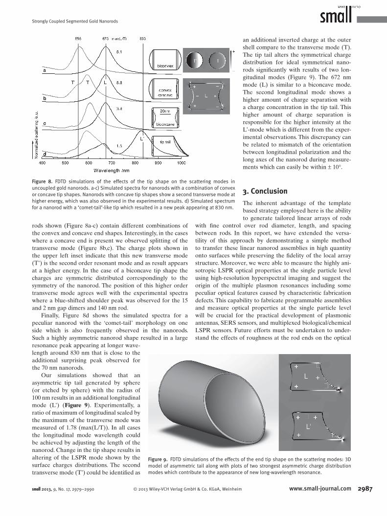
Figure 8 . FDTD simulations of the effects of the tip shape on the scattering modes in uncoupled gold nanorods. a-c) Simulated spectra for nanorods with a combination of convex or concave tip shapes. Nanorods with concave tip shapes show a second transverse mode at higher energy, which was also observed in the experimental results. d) Simulated spectrum for a nanorod with a ‘comet-tail’-like tip which resulted in a new peak appearing at 830 nm.
rods shown (Figure 8 a-c) contain different combinations of
the convex and concave end shapes. Interestingly, in the cases
where a concave end is present we observed splitting of the
transverse mode (Figure 8 b,c). The charge plots shown in
the upper left inset indicate that this new transverse mode
(T’) is the second order resonant mode and as result appears
at a higher energy. In the case of a biconcave tip shape the
charges are symmetric distributed correspondingly to the
symmetry of the nanorod. The position of this higher order
transverse mode agrees well with the experimental spectra
where a blue-shifted shoulder peak was observed for the 15
and 2 nm gap dimers and 140 nm rod.
Finally, Figure 8 d shows the simulated spectra for a
peculiar nanorod with the ‘comet-tail’ morphology on one
side which is also frequently observed in the nanorods.
Such a highly asymmetric nanorod shape resulted in a large
Figure 9 . FDTD simulations of the effects of the end tip shape on the scattering modes: 3D model of asymmetric tail along with plots of two strongest asymmetric charge distribution modes which contribute to the appearance of new long-wavelength resonance.
resonance peak appearing at longer wave-
length around 830 nm that is close to the
additional surprising peak observed for
the 70 nm nanorods.
Our simulations showed that an
asymmetric tip tail generated by sphere
(or etched by sphere) with the radius of
100 nm results in an additional longitudinal
mode (L’) ( Figure 9 ). Experimentally, a
ratio of maximum of longitudinal scaled by
the maximum of the transverse mode was
measured of 1.78 (max(L/T)). In all cases
the longitudinal mode wavelength could
be achieved by adjusting the length of the
nanorod. Change in the tip shape results in
altering of the LSPR mode shown by the
surface charges distributions. The second
transverse mode (T’) could be identifi ed as
© 2013 Wiley-VCH Verlag GmbH & Co. KGaA, Weinheismall 2013, 9, No. 17, 2979–2990
an additional inverted charge at the outer
shell compare to the transverse mode (T).
The tip tail alters the symmetrical charge
distribution for ideal symmetrical nano-
rods signifi cantly with results of two lon-
gitudinal modes (Figure 9 ). The 672 nm
mode (L) is similar to a biconcave mode.
The second longitudinal mode shows a
higher amount of charge separation with
a charge concentration in the tip tail. This
higher amount of charge separation is
responsible for the higher intensity at the
L’-mode which is different from the exper-
imental observations. This discrepancy can
be related to mismatch of the orientation
between longitudinal polarization and the
long axes of the nanorod during measure-
ments which can easily be within ± 10 ° .
3. Conclusion
The inherent advantage of the template
based strategy employed here is the ability
to generate tailored linear arrays of rods
with fi ne control over rod diameter, length, and spacing
between rods. In this report, we have extended the versa-
tility of this approach by demonstrating a simple method
to transfer these linear nanorod assemblies in high quantity
onto surfaces while preserving the fi delity of the local array
structure. Moreover, we were able to measure the highly ani-
sotropic LSPR optical properties at the single particle level
using high-resolution hyperspectral imaging and suggest the
origin of the multiple plasmon resonances including some
peculiar optical features caused by characteristic fabrication
defects. This capability to fabricate programmable assemblies
and measure optical properties at the single particle level
will be crucial for the practical development of plasmonic
antennas, SERS sensors, and multiplexed biological/chemical
LSPR sensors. Future efforts must be undertaken to under-
stand the effects of roughness at the rod ends on the optical
2987www.small-journal.comm

M. K. Gupta et al.
29
full papers
properties of template fabricated nanorods, especially in theregime of strong LSPR coupling. With further improvement
in the assembly of these segmented nanorods with long-
range order, this strategy has strong potential towards prac-
tical applications.
4. Experimental Section
All aqueous solutions were prepared using 18.2 ΜΩcm water obtained from a Barnstead Nanopure-UV system. Porous anodic alumina (PAA) templates were fabricated by anodization of 99.999% purity aluminum foils (as-rolled, 1 mm thickness from Goodfellow Corporation). The foil was cut into 3 cm x 4 cm cou-pons and degreased fi rst in acetone and then ethanol. A Keithley 2400 power supply was used to supply current and voltage for electropolishing and anodization steps. Coupons were electropo-lished in a solution comprised of 100 ml 60% perchloric acid solu-tion (Alfa Aesar) and 400 ml 99.9% ethanol ( Caution: vapor from perchloric acid can form explosive crystals! ) at 7 ° C by passing 1 A of current at 20 V for 15 min. [ 88 ] The coupons were then extensively rinsed in ethanol and dried in a nitrogen stream. Before anodiza-tion, one side of the coupons was protected with Tolber Miccro XP-2000 stop-off paint to prevent current leakage.
Anodization was performed in two stages using an aqueous 0.3 M oxalic acid (Alfa Aesar) solution at 15 ° C and 40 V. The fi rst anodization was carried out for 15 h to create well-ordered verti-cally oriented pores. After the fi rst anodization, the oxide layer was completely etched in a chromic acid solution (1.8 wt% Cr0 3 and 3.5 wt% H 3 PO 4 ) at 65 ° C for 2 h. The second anodization was car-ried out for 6 hours to achieve the desired membrane thickness of 40 micrometers. The pore side of the membrane was protected by spin coating a layer of cellulose acetate from a 3 wt% solution in acetone. The remaining back side aluminum was removed in a solution of 6 g CuCl 2 in 75 mL 38% HCl and 75 ml water. After completely removing the aluminum, the bottom side of the pores (adjacent to the aluminum) was opened in a 1 M NaOH solution for 2 min to yield through-hole pores. Finally, the protective cellulose acetate layer was dissolved in acetone, and the membrane was extensively rinsed in water and allowed to air dry.
Metal deposition was started by sputtering a 50 nm thick gold layer on the PAA template to serve as the working electrode and attached at the edge to a thin wire using conductive silver paste. A thick sacrifi cial nickel layer was then deposited from a commer-cial nickel sulfamate RTU solution (Technic Inc) by applying a -1.8 V potential using a Keithley 2400 sourcemeter for 10 min. This thick nickel layer served to seal the pores, allowing deposition to only occur inside the pores in the next step. The membrane was then mounted in a custom made Tefl on electrochemical cell with only the open side of the pores exposed to the electrolyte. Sequential nickel and gold depositions were carried out using commercial solutions from Technic as described above for nickel and Orotemp 24 RTU for gold. Depositions were performed at -0.9 V with respect to a saturated calomel reference electrode. A thin platinum foil was used as the counter electrode and potential was applied using a Gamry series G potentiostat. The total charge deposited was meas-ured real-time by the potentionstat and monitored to control the lengths of the individual segments. The cell was thoroughly rinsed in between segments to remove any residual electrolyte.
88 www.small-journal.com © 2013 Wiley-VCH V
After deposition, the wires were removed by fi rst dissolving the PAA template in 1 M NaOH containing 10 mg/mL PSS. Typically, a quarter of the sample area ( ∼ 1.25 cm 2 ) was dissolved in 1.5 mL of KOH/CTAB solution. The segmented rods were purifi ed by repeated centrifugation and rinsing. A total of 8 rinses were used: the initial 5 rinses were performed with 30 mg/mL CTAB solution to remove residual salt, next two rinses with water to remove excess CTAB, and fi nally rods were rinsed and dispersed in ethanol.
PS fi lms were spin cast on freshly piranha cleaned glass or silicon substrates using a 1 wt% solution of 250,000 MW PS in tol-uene at 3000 rpm. The PS coated substrates were then placed on a hotplate at 150 ° C and were allowed to equilibrate for 5-10 min. The segmented rod ethanol dispersion was then deposited drop-wise on the heated substrates to embed the rods in the PS layer. Once embedded, the nickel segments were etched in 38% HCl for 1-2 min with extensive rinsing in water afterwards to remove any residue.
SEM images were collected using a Zeiss Ultra 60 FE-SEM and a Hitachi S-3400 SEM with accelerating voltage typically at 5–10 kV and working distance of 5-7 mm. Dark-fi eld imaging (100 × ) of gold nanorods was done using an Olympus BX-51 micro-scope and 100 W quartz halogen light source on a CytoViva micro-scope and software. Spectral data were captured with a CytoViva spectrophotometer and integrated CCD camera. Each spectrum shown represents a single pixel imaged with a 100 × objective and approximately 64 nm in size. Samples were prepared on glass slides to allow scattering measurements to be performed in trans-mission mode. The sample was covered with type A immersion oil and then covered with a cover slip and sealed with nail polish to minimize disturbances. Each spectra is normalized by dividing it by a reference region (identical width, but with no particles). Spectral analysis was performed with the CytoViva Hyperspectral analysis software (ENVI) program. For polarized dark-fi eld scattering meas-urements, the incident light was polarized with a linear polarizer. The direction of polarization was rotated between 0–360 ° .
High Angle Annular Dark Field-Scanning Transmission Electron Microscopy (HAADF-STEM) was performed on a 300 kV Cs-corrected FEI Titan. Spot size 9, a convergence angle of 7.2 mrad, and an annular detector camera length of 105 mm, and a Fischione model 3000 PMT detector were used to collect the images.
The optical response of gold nanorods with varying interpar-ticle separation was calculated using the DDA method with the DDSCAT 6.1 code offered publicly by Draine and Flatau. The die-lectric values for gold reported by Johnson and Christy were used and the medium surrounding the particle was represented as oil with a refractive index of 1.51. For calculation of the scattering spectra and the surface charges distributions, we used the com-mercial software from Lumerical Solutions Inc. (FDTD Solutions, Version 7.5.7). The nanorod models were designed in SolidWorks (Education Edition, 2012 SP 3.0). The data were saved in the STereoLithography (STL) format and afterwards converted into a Lumerical Solutions Inc. readable fi le format called Graphic Data-base System (GDSII) format via STL2GDS from Artwork Conversion (Version 1.24). According to the GDSII data format the nanorods were sliced in 1 or 0.5nm thickness (corresponding to simulation mesh), respectively. Longitudinal and transversal modes were sim-ulated by the corresponding polarization.
Simulations with an edge rounding of 4nm of the concave tip face were set to 1nm mesh size. Mesh size of the tip tail was set
erlag GmbH & Co. KGaA, Weinheim small 2013, 9, No. 17, 2979–2990

Strongly Coupled Segmented Gold Nanorods
[ 1 ] N. J. Halas , S. Lal , W. S. Chang , S. Link , P. Nordlander , Chem. Rev. 2011 , 111 , 3913 .
[ 2 ] R. Elghanian , J. J. Storhoff , R. C. Mucic , R. L. Letsinger , C. A. Mirkin , Science 1997 , 277 , 1078 .
[ 3 ] S. Nie , S. R. Emory , Science 1997 , 275 , 1102 . [ 4 ] M. K. Gupta , S. Chang , S. Singamaneni , L. F. Drummy , R. Gunaw-
idjaja , R. R. Naik , V. V. Tsukruk , Small 2011 , 7 , 1192 . [ 5 ] S. Chang , H. Ko , R. Gunawidjaja , V. V. Tsukruk , J. Phys. Chem. C
2011 , 115 , 4387 . [ 6 ] A. M. Funston , C. Novo , T. J. Davis , P. Mulvaney , Nano Lett. 2009 ,
9 , 1651 . [ 7 ] B. Willingham , D. W. Brandl , P. Nordlander , Appl. Phys. B 2008 ,
93 , 209 . [ 8 ] K. C. Woo , L. Shao , H. Chen , Y. Ling , J. Wang , H.-Q. Lin , ACS Nano
2011 , 5 , 5976 . [ 9 ] P. K. Jain , M. A. El-Sayed , J. Phys. Chem. C 2008 , 112 , 4954 . [ 10 ] J. A. Schuller , E. S. Barnard , W. Cai , Y. C. Jun , J. S. White ,
M. L. Brongersma , Nat. Mater. 2010 , 9 , 193 . [ 11 ] H. A. Atwater , A. Polman , Nat. Mater. 2010 , 9 , 205 . [ 12 ] J. N. Anker , W. Paige Hall , O Lyandres , N. C. Shah , J. Zhao , R. P. Van
Duyne , Nat. Mater. 2008 , 7 , 442 . [ 13 ] R. A. Alvarez-Puebla , L. M. Liz-Marzan , Small 2010 , 6 , 604 . [ 14 ] H. Ko , S. Singamaneni , V. V. Tsukruk , Small 2008 , 4 , 1576 . [ 15 ] R. Gunawidjaja , S. Peleshanko , H. Ko , V. V. Tsukruk , Adv. Mater.
2008 , 20 , 1544 . [ 16 ] H. Ko , S. Chang , V. V. Tsukruk , ACS Nano 2009 , 3 , 181 . [ 17 ] S. Chang , H. Ko , S. Singamaneni , R. Gunawidjaja , V. V. Tsukruk ,
Anal. Chem. 2009 , 81 , 5740 . [ 18 ] W. Rechberger , A. Hohenau , A. Leitner , J. R. Krenn , B. Lamprecht ,
F. R. Aussenegg , Opt. Commun. 2003 , 220 , 137 . [ 19 ] P. K. Jain , W. Huang , M. A. El-Sayed , Nano Lett. 2007 , 7 , 2080 . [ 20 ] P. K. Jain , M. A. El-Sayed , Chem. Phys. Lett. 2010 , 487 , 153 . [ 21 ] C. Tabor , D. Van Haute , M. A. El-Sayed , ACS Nano 2009 , 3 , 3670 . [ 22 ] R. Near , C. Tabor , J. Duan , R. Pachter , M. A. El-Sayed , Nano Lett.
2012 , 12 , 2158 . [ 23 ] V. M. Shalaev , W. Cai , U. K. Chettiar , H. K. Yuan , A. K. Sarychev ,
V. P. Drachev , A. V. Kildishev , Opt. Lett. 2005 , 30 , 3356 . [ 24 ] J. B. Lassiter , H. Sobhani , J. A. Fan , J. Kundu , F. Capasso ,
P. Nordlander , N. J. Halas , Nano Lett. 2010 , 10 , 3184 .
to 0.5nm for best possible rendering of the edges. First conformal variant was used for mesh refi nement. The mesh size was stretched above the whole fi eld source with the following x-y-z-dimensions: 200, 150 and 150nm (x-axes correspond to the longitudinal axes). All simulations were well converged below the simulation time of 75fs at an auto shutoff level of 10 − 5 . As boundary conditions perfect match layer (PML) was used. The gold permittivity was chosen from Johnson and Christy [ 89 ] and fi tted by a 8 coeffi cient function showing an RMS error of 0.206 at a fi tting range between 400 and 1000 nm. The background index was chosen over the mentioned spectra according to the experimentally used oil index (1.515). [ 90 , 91 ]
Acknowledgements
We would like to thank for support the FA9550-11-1-0233 and FA9550-09-1-0162 (BIONIC Center) from Air Force Offi ce of Scien-tifi c Research and Air Force Research Lab. We acknowledge J. Dene-ault and Dr. M. Durstock for help in preparation of porous anodic alumina templates.
© 2013 Wiley-VCH Verlag GmbHsmall 2013, 9, No. 17, 2979–2990
[ 25 ] Z. Fang , J. Cai , Z. Yan , P. Nordlander , N. J. Halas , X. Zhu , Nano Lett. 2011 , 11 , 4475 .
[ 26 ] J. Ye , F. Wen , H. Sobhani , J. B. Lassiter , P. Van Dorpe , P. Nordlander , N. J. Halas , Nano Lett. 2012 , 12 , 1660 .
[ 27 ] B. Luk’yanchuk , N. I. Zheludev , S. A. Maier , N. J. Halas , P. Nordlander , H. Giessen , C. T. Chong , Nat. Mater. 2010 , 9 , 707 .
[ 28 ] P. Nagpal , N. C. Linkquist , S.-H. Oh , D. J. Norris , Science 2009 , 325 , 594 .
[ 29 ] K. Kiu , Z. Nie , N. Zhao , W. Li , M. Rubinstein , E. Kumacheva , Sci-ence 2010 , 329 , 197 .
[ 30 ] Z. Nie , D. Fava , M. Rubinstein, E. Kumacheva, J. Am. Chem. Soc. 2008 , 130 , 3683.
[ 31 ] A. P. Alivisatos , K. P. Johnsson , X. Peng , T. E. Wilson , C. J. Loweth , M. P. Bruchez , P. G. Schultz , Nature 1996 , 382 , 609 .
[ 32 ] S. Y. Park , A. K. R. Lytton-Jean , B. Lee , S. Weigand , G. C. Schatz , C. A. Mirkin , Nature 2008 , 451 , 553 .
[ 33 ] D. Nykpanchuk , M. M. Maye , D. van der Lelie , O. Gang , Nature 2008 , 451 , 549 .
[ 34 ] A. Guerrero-Martinez , J. Perez-Juste , E. Carbo-Argibay , G. Tardajos , L. M. Liz-Marzan , Angew. Chem. Int. Ed. 2009 , 48 , 9484 .
[ 35 ] S. Pal , Z. Deng , H. Wang , S. Zou , Y. Liu , H. Yan , J. Am. Chem. Soc. 2011 , 133 , 1706 .
[ 36 ] J. M. Slocik , F. Tam , N. J. Halas , R. R. Naik , Nano Lett. 2007 , 7 , 1054 .
[ 37 ] M. P. Busson , B. Rolly , B. Stout , N. Bonod , E. Larquet , A. Polman , S. Bidault , Nano Lett. 2011 , 11 , 5060 .
[ 38 ] M. Rycenga , J. M. McLellan , Y. Xia , Adv. Mater. 2008 , 20 , 2416 . [ 39 ] D. Nepal , K. Park , R. A. Vaia , Small 2012 , 8 , 1013 . [ 40 ] N. Gandra , A. Abbas , L. Tian , S. Singamaneni , Nano Lett. 2012 ,
12 , 2645 . [ 41 ] R. J. Macfarlane , B. Lee , M. R. Jones , N. Harris , G. C. Schatz ,
C. A. Mirkin , Science 2011 , 334 , 204 . [ 42 ] K. Park , H. Koerner , R. A. Vaia , Nano Lett. 2010 , 10 , 1433 . [ 43 ] D. Nepal , M. S. Onses , K. Park , M. Jespersen , C. J. Thode ,
P. F. Nealey , R. A. Vaia , ACS Nano 2012 , 6 , 5693 . [ 44 ] C. Kuemin , L. Nowack , L. Bozano , N. D. Spencer , H. Wolf , Adv.
Funct. Mater. 2012 , 22 , 702 . [ 45 ] T. Thai , Y. Zheng , S. H. Ng , S. Mudie , M. Altissimo , U. Bach ,
Angew. Chem. Int. Ed. 2012 , 51 , 8732 . [ 46 ] Z. Sun , W. Ni , Z. Yang , X. Kou , L. Li , J. Wang , Small 2008 , 4 , 1287 . [ 47 ] S. Chang , S. Singamaneni , E. Kharlampieva , S. L. Young ,
V. V. Tsukruk , Macromolecules 2009 , 42 , 5781 . [ 48 ] C. R. Martin , Science 1994 , 266 , 1961 . [ 49 ] M. R. Jones , K. D. Osberg , R. J. Macfarlane , M. R. Langille ,
C. A. Mirkin , Chem. Rev. 2011 , 111 , 3736 . [ 50 ] S. J. Hurst , E. K. Payne , L. Qin , C. A. Mirkin , Angew. Chem. Int. Ed.
2006 , 45 , 2672 . [ 51 ] T. R. Kline , M. Tian , J. Wang , A. Sen , M. W. H. Chan , T. E. Mallouk ,
Inorg. Chem. 2006 , 45 , 7555 . [ 52 ] L. Jiang , Y. Sun , F. Huo , H. Zhang , L. Qin , S. Li , X. Chen , Nanoscale
2012 , 4 , 66 . [ 53 ] D. AlMawlawi , N. Coombs , M. Moskovits , J. Appl. Phys. 1991 , 70 ,
4421 . [ 54 ] S. R. Nicewarner-Pena , R. G. Freeman , B. D. Reiss , L. He , D. J. Pena ,
I. D. Walton , R. Cromer , C. D. Keating , M. J. Natan , Science 2001 , 294 , 137 .
[ 55 ] R. Elnathan , R. Kantaev , F. Patolsky , Nano Lett. 2008 , 8 , 3964 . [ 56 ] W. Lee , R. Scholz , K. Nielsch , U. Gosele , Angew. Chem. Int. Ed.
2005 , 44 , 6050 . [ 57 ] C. D. Keating , M. J. Natan , Adv. Mater. 2003 , 15 , 451 . [ 58 ] S. Kim , K. L. Shuford , H.-M. Bok , S. K. Kim , S. Park , Nano Lett.
2008 , 8 , 800 . [ 59 ] S. Kim , S. K. Kim , S. Park , J. Am. Chem. Soc. 2009 , 131 , 8380 . [ 60 ] A. L. Schmucker , N. Harris , M. J. Banholzer , M. G. Blaber ,
K. D. Osberg , G. C. Schatz , C. A. Mirkin , ACS Nano 2010 , 4 , 5453 . [ 61 ] S. Liu , J. B.-H. Tok , Z. Bao , Nano Lett. 2005 , 5 , 1071 . [ 62 ] L. Qin , S. Park , L. Huang , C. A. Mirkin , Science 2005 , 309 , 113 .
2989www.small-journal.com & Co. KGaA, Weinheim

M. K. Gupta et al.
2
full papers
[ 63 ] T. Mirkovic , M. L. Foo , A. C. Arsenault , S. Fournier-Bidoz ,N. S. Zacharia , G. A. Ozin , Nat. Nanotech. 2007 , 2 , 565 . [ 64 ] K. D. Osberg , A. L. Schmucker , A. J. Senesi , C. A. Mirkin , Nano
Lett. 2011 , 11 , 820 . [ 65 ] L. Qin , J.-W. Jang , L. Huang , C. A. Mirkin , Small 2007 , 3 , 86 . [ 66 ] L. Qin , M. J. Banholzer , J. E. Millstone , C. A. Mirkin , Nano Lett.
2007 , 7 , 3849 . [ 67 ] M. J. Banholzer , K. D. Osberg , S. Li , B. F. Mangelson , G. C. Schatz ,
C. A. Mirkin , ACS Nano 2010 , 4 , 5446 . [ 68 ] W. Wei , S. Z. Li , L. D. Qin , C. Xue , J. E. Millstone , X. Y. Xu ,
G. C. Schatz , C. A. Mirkin , Nano Lett. 2008 , 8 , 3446 . [ 69 ] L. Qin , S. Zou , C. Xue , A. Atkinson , G. C. Schatz , C. A. Mirkin , Proc.
Natl. Acad. Sci. USA 2006 , 103 , 13300 . [ 70 ] D. M. O’Carroll , C. E. Hofmann , H. A. Atwater , Adv. Mater. 2010 ,
22 , 1223 . [ 71 ] M. L. Pedano , S. Li , G. C. Schatz , C. A. Mirkin , Angew. Chem. Int.
Ed. 2010 , 49 , 78 . [ 72 ] W. Wei , S. Z. Li , J. E. Millstone , M. J. Banholzer , X. D. Chen , X. Y. Xu ,
G. C. Schatz , C. A. Mirkin , Angew. Chem. Int. Ed. 2009 , 48 , 4210 . [ 73 ] M. J. Banholzer , L. Qin , J. E. Millstone , K. D. Osberg , C. A. Mirkin ,
Nat. Prot. 2009 , 4 , 838 . [ 74 ] K. D. Osberg , M. Rycenga , N. Harris , A. L. Schmucker , M. R. Langille ,
G. C. Schatz , C. A. Mirkin , Nano Lett. 2012 , 12 , 3828 . [ 75 ] A. Gole , C. J. Murphy , Chem. Mater. 2005 , 17 , 1325 – 1330 . [ 76 ] A. M. Alkilany , L. B. Thompson , C. J. Murphy , ACS Appl. Mater.
Interfaces 2010 , 2 , 3417 . [ 77 ] S. Vial , I. Pastoriza-Santos , J. Perez-Juste , L. M. Liz-Marzan ,
Langmuir 2007 , 23 , 4606 .
990 www.small-journal.com © 2013 Wiley-VCH Ve
[ 78 ] V. Kozlovskaya , E. Kharlampieva , B. P. Khanal , P. Manna , E. R. Zubarev , V. V. Tsukruk , Chem. Mater. 2008 , 20 , 7474 .
[ 79 ] L. Tian , M. Fei , R. Kattumenu , A. Abbas , S. Singamaneni , Nano-technology 2012 , 23 , 255502 .
[ 80 ] J. Lim , C. Lanni , E. R. Evarts , F. Lanni , R. D. Tilton , S. A. Majetich , ACS Nano 2011 , 5 , 217 .
[ 81 ] P. K. Jain , S. Eustis , M. A. El-Sayed , J. Phys. Chem. B 2006 , 110 , 18243 .
[ 82 ] A. S. Stender , G. Wang , W. Sun , N. Fang , ACS Nano 2010 , 4 , 7667 .
[ 83 ] O. L. Muskens , G. Bachelier , N. Del Fatti , F. Vallée , A. Brioude , X. Jiang , M. P. Pileni , J. Phys. Chem. C 2008 , 112 , 8917 .
[ 84 ] S. Link , M. B. Mohamed , M. A. El-Sayed , J. Phys. Chem. B 1999 , 103 , 3073 .
[ 85 ] J.-M. Moon , A. Wei , J. Phys. Chem. B 2005 , 109 , 23336 . [ 86 ] K.-S. Lee , M. A. El-Sayed , J. Phys. Chem. B 2005 , 109 ,
20331 . [ 87 ] S. Link , M. A. El-Sayed , J. Phys. Chem. B 1999 , 103 , 8410 . [ 88 ] A. P. Li , F. Müller , A. Birner , K. Nielsch , U. Gösele , J. Appl. Phys.
1998 , 84 , 6023 . [ 89 ] P. B. Johnson , R. W. Christy , Phys. Rev. B 1972 , 6 , 4370 . [ 90 ] S. A. Maier , M. L. Brongersma , P. R. Kik , H. A. Atwater , Phys. Rev.
B 2002 , 65 , 193408 . [ 91 ] L. Slaughter , W.-S. Chang , S. Link , J. Phys. Chem. Lett. 2011 , 2 ,
2015 .
Received: January 23, 2013 Published online: March 12, 2013
rlag GmbH & Co. KGaA, Weinheim small 2013, 9, No. 17, 2979–2990


![Enhancing the Angular Sensitivity of Plasmonic Sensors ...biotheory.phys.cwru.edu/PDF/AOM.pdf · ultrasensitive plasmonic biosensors.[29,30] A plasmonic nanorod metamaterial (Type](https://img.pdfslide.net/doc/110x75/5fcdd2c6db367d06a677e7be/enhancing-the-angular-sensitivity-of-plasmonic-sensors-ultrasensitive-plasmonic.jpg)