Embed Size (px)
Citation preview
Int. J. Electrochem. Sci., 6 (2011) 3564 - 3579
International Journal of
ELECTROCHEMICAL SCIENCE
www.electrochemsci.org
Surface Morphology and Electrical Properties of Pulse
Electrodeposition of NiFe Films on Copper Substrates in
Ultrasonic Field
R.Balachandran1,*
, H.K.Yow2, B.H.Ong
1, K.B.Tan
3, K.Anuar
3, H.Y.Wong
1
1Faculty of Engineering, Multimedia University, Cyberjaya, 63100, Malaysia
2Department of Electrical and Electronic Engineering, Faculty of Engineering and Science, Universiti
Tunku Abdul Rahman, Kuala Lumpur Campus, 53300, Kuala Lumpur, Malaysia 3Department of Chemistry, Universiti Putra Malaysia, Serdang, 43400, Malaysia
*E-mail: [email protected]
Received: 4 February 2011 / Accepted: 2 July 2011 / Published: 1 August 2011
NiFe films were pulse electrodeposited on conductive copper substrates under galvanostatic mode with
and without the presence of an ultrasonic field at different pulse current magnitudes and duty cycles.
The optimum deposition condition was found to be at a current magnitude of 40 mA and a duty cycle
of 50.00% under ultrasonic treatment. This deposition condition has significantly reduced the surface
roughness from 39.01 1.1 nm to 6.96 1.1 nm and the spherical grain size in the range from 579.40
nm – 623.30 nm to 29.00 nm – 46.90 nm. On the other hand, the resistivity was reduced to 19.86
µcm from 54.00 µcm as the Ni content increased from 76.08% to 80.12 % for achieving good
stoichiometry for NiFe thin films. Through the optimization study, the deposition current is observed
to be the dominant factor in determining the single phase deposition of NiFe film whereas ultrasonic
field and duty cycle significantly reduces the surface roughness and the spherical grain size, all of
which combine to reduce film resistivity.
Keywords: NiFe thin films, electrochemical reactions, electrode materials, surface morphology,
surface roughness, resistivity
1. INTRODUCTION
NiFe thin films have attracted tremendous interest in electrical and electronic applications
including hard disk, magnetic shielding and electrode for capacitors. The electrical properties of NiFe
thin films rely strongly on the composition and processing control. The surface roughness of thin films
has significant influence on the resistivity of the films. It had been reported that film resistivity showed
an approximately linear relationship with surface roughness [1]. Hence, the reduction in surface
Int. J. Electrochem. Sci., Vol. 6, 2011
3565
roughness should lead on to a decrease in the film resistivity. It was reported that ultrasonic treatment
during film deposition could improve film uniformity and better crystallinity [2]. On the other hand,
electroplating of permalloy, which has a Ni and Fe alloy ratio of 80/20, is cost effective with relative
ease of process control, as compared to physical vapor deposition [3].
In our previous works, NiFe film was successfully pulse electrodeposited on copper (Cu)
substrate under galvanostatic mode in the presence of ultrasonic field at a current magnitude of 35 mA
and a duty cycle (D) of 50 % [4]. Factors influencing the electro-deposition were found to include the
current density, the applied potential, the temperature, the bath composition, the molar concentration of
the electrolyte, substrates and impurities. In this work, the process control is optimized by varying the
primary factors such as the applied current for the galvanostatic mode, the duty cycle of the pulse (or
the deposition time) and the external ultrasonic field. However, other parameters such as potential,
temperature, molar concentration and bath composition remain constant. NiFe films were pulse
electrodeposited under galvanostatic mode on conductive Cu substrates with and without the ultrasonic
field for current magnitudes of 20 mA, 30 mA, 33 mA, 35 mA and 40 mA at duty cycles of 66.67%
and 50.00% for 2 minutes, respectively.
Cu is chosen as the substrate because it exhibits excellent thermal and conductive behavior,
thus improving the carrier collection efficiency [5]. Ultrasonic field is expected to improve the coating
surface and shorten the coating duration due to higher plating current efficiency [6]. A high proportion
of loosely attached sediments deposited on the thin films could therefore be removed in which better
crystallinity and film uniformity is achievable [2]. The NiFe film electrodeposited with the ultrasonic
environment has shown significantly improved surface quality with an average grain size below 100
nm. Higher Ni content in NiFe film is also expected to reduce the leakage current density [7] if NiFe is
used as an electrode in the capacitors.
There are reported studies on the deposition of NiFe thin films by R.F. plasma sputtering [8],
ion-beam sputtering [9], electrodeposition technique [10, 11], conventional R.F. diode sputtering
system [12], metal oxide chemical vapor deposition (MOCVD) technique [13] , DC magnetron
sputtering technique [13] and others. The resistivities of Ni81Fe19, and Ni80Fe15Mo5 thin films
deposited on silicon by r.f. plasma sputtering were determined as 20 µcm. NiFe thin films deposited
using ion-beam sputtering showed a slightly higher resistivity, i.e., within 20-24 µcm [9]. The
NixFe1-x (0.22x 0.62) alloy films grown by electrodeposition technique [10] were improved
drastically where resistivities dropped to 17 µcm from 89 µcm and Ni content increased from 22 to
64%. The [Fe20Ni80/SiO2]xN multilayer films were prepared using a conventional R.F. diode sputtering
system and the as-deposited thin film resistivity was found to be 980 µcm. It shows that the
resistivity decreases as the percentage of Ni content increases. The atomic force microscopy (AFM)
results showed that the surface root mean square roughness of the MOCVD epitaxial films was found
to be in the range of 6.5 to 11.5 nm for the electrodeposited NiFe thin films.
In consideration of our previous works, the optimization and process control of NiFe film are
yet to be explored in detail. Hence, we investigated different parameters, e.g. current magnitude, duty
cycle and the effect of ultrasonic field to achieve a closer match to the reported permalloy composition
[Ni80Fe20] with lower resistivity and surface roughness.

Int. J. Electrochem. Sci., Vol. 6, 2011
3566
2. EXPERIMENTAL
The Copper foils of 2.54 cm x 2.54 cm were used as bottom substrates of NiFe thin films. The
pulse frequency of 1 Hz was generated from the AutoLab system for pulse electrodeposition of NiFe
thin films. The concentration of Ni/Fe cations in the bath was fixed as 0.05M and 0.01M, respectively.
The details of the experimental work have been described elsewhere [4]. Pulse electrodeposition of
NiFe films was carried out at room temperature for 2 minutes in galvanostatic mode for current
magnitudes of 20 mA, 30 mA, 33 mA, 35 mA and 40 mA, and at duty cycles of 66.67% and 50.00%,
without and with the presence of an ultrasonic field, respectively. The electrochemical cell was
maintained at a pH of 3.0 (acidic) where additional sulphuric acid was added if necessary. The
ultrasonic field was generated using an ultrasonic bath (Powersonic 405) at an ultrasonic frequency of
40 kHz and the bath temperature was maintained at 27 C.
As-prepared NiFe films, with and without the presence of an ultrasonic field, were examined
using X-ray diffractometer (XRD, Phillips X’Pert PRO) in the 2 range of 20 - 80. Scanning electron
microscopy (SEM, Leo 1450 VPSEM) was employed for surface morphology study. Surface
roughness measurements were conducted by atomic force microscopy (AFM, Quesant q-scope 250) in
contact mode. Energy dispersive X-ray spectroscopy (EDS, Oxford Instruments, 7353) was used for
elemental analysis. Electrical properties of the prepared samples were characterized by four-point
probe (FPP, Keithley 2400 source, close cryogenic system model CS202-X1 AL JEN, DE-202AE
expander with precise temperature control Lakeshore 325).
3. RESULTS AND DISCUSSION
3.1 Phase analysis
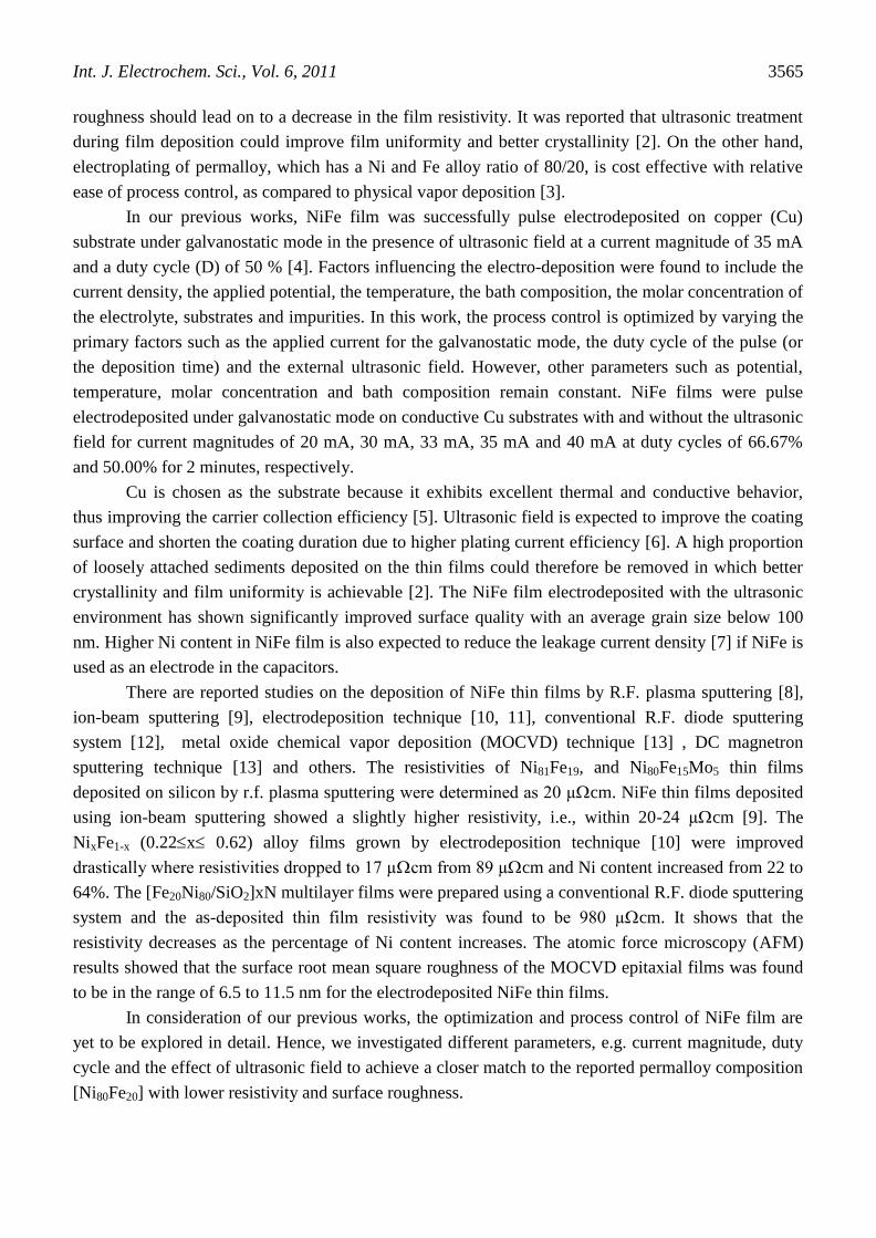
Figs. 1a and 1b show the potential versus time (V–t) plots for the pulse electrodeposition of
NiFe thin films at a current magnitude of 40 mA with duty cycles of 66.67% and 50.00% under
ultrasonic field, respectively with the applied potential ranging from -1.224 V to -3.357 V. It is
evidently shown that duty cycle plays an important role in the rate of film deposition on the Cu
substrate. With ultrasonication and increased duty cycle, the rate of NiFe deposition on Cu substrate
increased rapidly as the charge-discharge time for the double layer are found to be smaller.
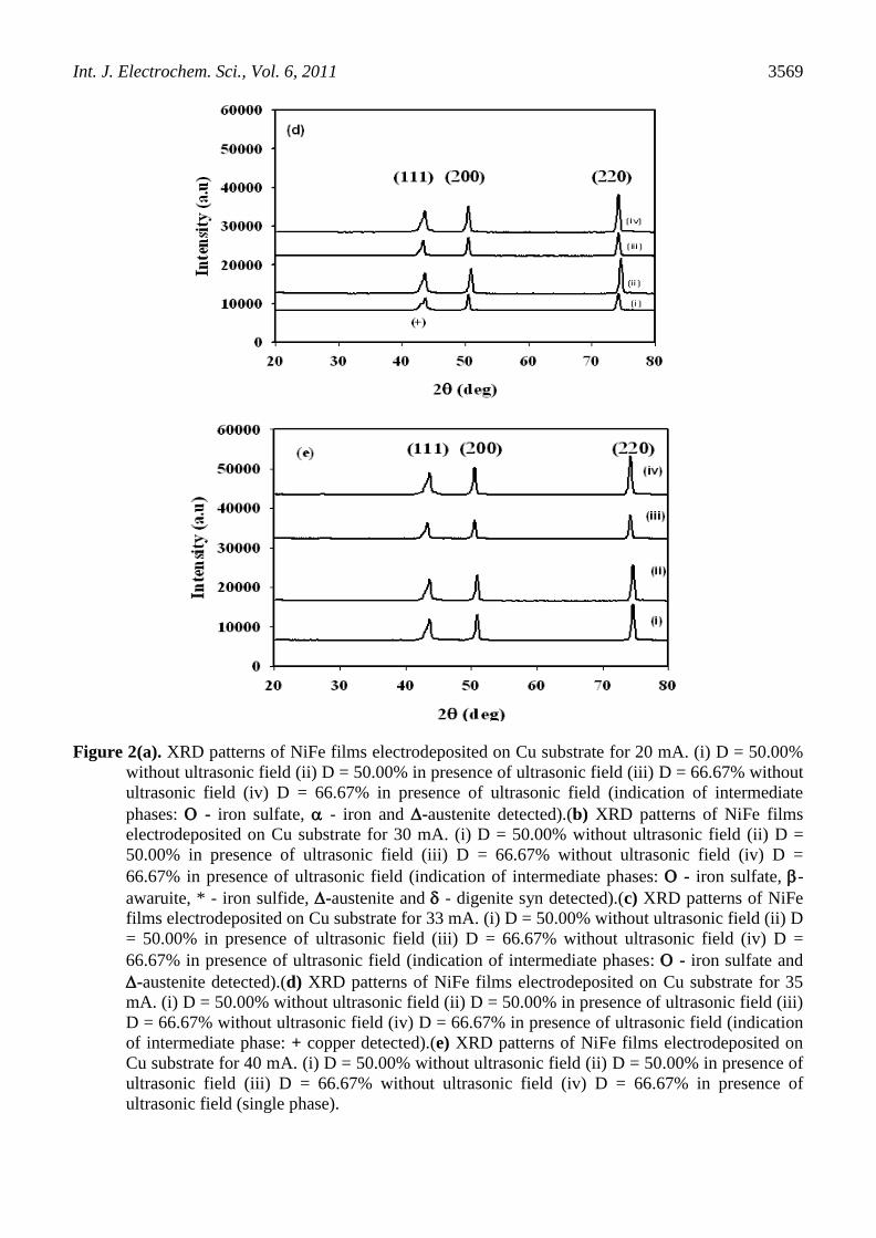
The X-ray powder diffraction patterns of NiFe film electrodeposited on Cu substrates using
different currents, and duty cycles are shown in Figures 2a-e. When a current of 20 mA and a 50.00 %
duty cycle were applied, minute traces of second phases, iron sulphate (ICDD number: 01-0703) at
27.421 and iron (ICDD number: 01-089-4185) at 42.898 are discernable if no ultrasonic field was
applied during the film deposition. (Fig.2ai). However, if the duty cycle was increased to 66.67 %
under ultrasonic field, these two phases were removed and only the second phase of austenite (ICDD
number: 52-0513) is discernable at 42.759.
Int. J. Electrochem. Sci., Vol. 6, 2011
3567
When a current of 30 mA and a 50.00 % duty cycle were applied, major diffraction planes of
NiFe are observed as indicated in Fig.2b (i) and (ii). However, second phase, awaruite (ICDD number,
39-0419) is detected at 2, 44.279 if no ultrasonic field was applied (Fig. 2b).
(a)
(b)
Figure 1. Potential – time graph of NiFe films electrodeposited on Cu substrates with ultrasonic filed
for a current magnitude of 40 mA and duty cycle of (a) 66.67% and (b) 50.00%.

Int. J. Electrochem. Sci., Vol. 6, 2011
3568
Int. J. Electrochem. Sci., Vol. 6, 2011
3569
Figure 2(a). XRD patterns of NiFe films electrodeposited on Cu substrate for 20 mA. (i) D = 50.00%
without ultrasonic field (ii) D = 50.00% in presence of ultrasonic field (iii) D = 66.67% without
ultrasonic field (iv) D = 66.67% in presence of ultrasonic field (indication of intermediate
phases: - iron sulfate, - iron and -austenite detected).(b) XRD patterns of NiFe films
electrodeposited on Cu substrate for 30 mA. (i) D = 50.00% without ultrasonic field (ii) D =
50.00% in presence of ultrasonic field (iii) D = 66.67% without ultrasonic field (iv) D =
66.67% in presence of ultrasonic field (indication of intermediate phases: - iron sulfate, -
awaruite, * - iron sulfide, -austenite and - digenite syn detected).(c) XRD patterns of NiFe
films electrodeposited on Cu substrate for 33 mA. (i) D = 50.00% without ultrasonic field (ii) D
= 50.00% in presence of ultrasonic field (iii) D = 66.67% without ultrasonic field (iv) D =
66.67% in presence of ultrasonic field (indication of intermediate phases: - iron sulfate and
-austenite detected).(d) XRD patterns of NiFe films electrodeposited on Cu substrate for 35
mA. (i) D = 50.00% without ultrasonic field (ii) D = 50.00% in presence of ultrasonic field (iii)
D = 66.67% without ultrasonic field (iv) D = 66.67% in presence of ultrasonic field (indication
of intermediate phase: + copper detected).(e) XRD patterns of NiFe films electrodeposited on
Cu substrate for 40 mA. (i) D = 50.00% without ultrasonic field (ii) D = 50.00% in presence of
ultrasonic field (iii) D = 66.67% without ultrasonic field (iv) D = 66.67% in presence of
ultrasonic field (single phase).
Int. J. Electrochem. Sci., Vol. 6, 2011
3570
On the other hand, additional iron sulphide (ICDD number: 23-1123) at 28.494 and austenite
(ICDD number 52-0513) at 42.759 are discernable if a 50.00% duty cycle was applied under the
presence of ultrasonic field.
If the duty cycle was further increased to 66.67 %, awaruite phase diminishes and iron sulphate
(ICDD number 01-0703) at 27.421 was then formed (Fig. 2biii). Iron sulfide and iron sulfate are
replaced by digenite syn (ICDD number: 89-2072) at 46.1054 for the sample under application of
ultrasonic field (Fig. 2biv). These X-ray results interestingly show that the formation of secondary
phases is greatly influenced by the control of different parameters. From Fig. 2c, it is observed that
when a current of 33 mA and a duty cycle of 50.00% were applied without ultrasonication, austenite
phase is discernable at 2 42.579 (Fig.2ci).
Meanwhile, results similar to that of the thin films deposited under lower current magnitude
and ultrasonication are obtained. It is then expected that the phase of iron sulfate could only be
removed by the increase of the duty cycle. In addition, pure single phase NiFe film has yet to be
produced and therefore higher current is required.
Single phase Ni80Fe20 are obtained, when the current magnitude applied is 35 mA, for samples
which are under the influence of ultrasonic field (Fig. 2d). It is observed that all the diffraction peaks
corresponding to (1 1 1), (2 0 0), and (2 2 0) planes could be fully indexed based on the reported ICDD
00-003-1209. For the NiFe films electrodeposited without the ultrasonic environment, there is a minor
peak of Cu substrate at the ‘knee-point’ next to the major diffraction peak corresponding to the (1 1 1)
diffraction when a duty cycle of 50.00% was applied (Fig. 2di). The 2 value for the knee-point is
found to be 43.325 (ICDD number: 00-004-836).
The result shows that it is more difficult to obtain a close match to Ni80Fe20, without the use of
ultrasonic field. In comparison, no trace of Cu was observed in the XRD pattern of Ni80Fe20 with
ultrasonic effect as the surface is homogenous due to the higher mass transport. In addition, the
diffraction peaks show much lower intensity and thus, an indication of poorer crystalline quality.
However, the diffraction peak for the film corresponding to a duty cycle of 50.00% in the presence of
the ultrasonic field is higher than that of the 66.67% thin film without ultrasonic field. It shows that
ultrasonic filed has improved the crystallinity.
When a current of 40 mA current was applied (Fig.2e), single phase Ni80Fe20 are obtained,
irrespective of duty cycle and the external ultrasonic field. The estimated crystallite size by Scherrer’s
formula is in range of 15.80 0.1 nm for both films deposited with and without the ultrasonic field
when the current amplitude is 40 mA.
It has been concluded in the phase analysis of NiFe thin films on copper substrates that current
magnitude is a dominant factor in influence formation of single phase Ni80Fe20 thin films, besides duty
cycle and the external applied ultrasonic field. When the current magnitude is 35 mA, irrespective of
the external applied ultrasonic field, single phase Ni80Fe20 was obtained at a duty cycle of 66.67 %.
(Fig.2diii-iv). However, the NiFe deposited on copper substrate under the influence of ultrasonic field
shows better crystallinity as sharper and higher intensity diffraction planes are discernable. As
observed, the crystallinity improved in the presence of the ultrasonic field and when the duty cycle was
increased.
Int. J. Electrochem. Sci., Vol. 6, 2011
3571
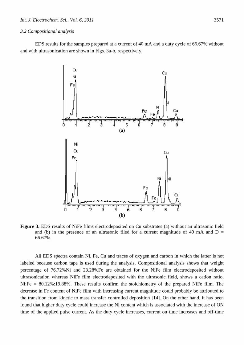
3.2 Compositional analysis
EDS results for the samples prepared at a current of 40 mA and a duty cycle of 66.67% without
and with ultrasonication are shown in Figs. 3a-b, respectively.
(a)
(b)
Figure 3. EDS results of NiFe films electrodeposited on Cu substrates (a) without an ultrasonic field
and (b) in the presence of an ultrasonic filed for a current magnitude of 40 mA and D =
66.67%.
All EDS spectra contain Ni, Fe, Cu and traces of oxygen and carbon in which the latter is not
labeled because carbon tape is used during the analysis. Compositional analysis shows that weight
percentage of 76.72%Ni and 23.28%Fe are obtained for the NiFe film electrodeposited without
ultrasonication whereas NiFe film electrodeposited with the ultrasonic field, shows a cation ratio,
Ni:Fe = 80.12%:19.88%. These results confirm the stoichiometry of the prepared NiFe film. The
decrease in Fe content of NiFe film with increasing current magnitude could probably be attributed to
the transition from kinetic to mass transfer controlled deposition [14]. On the other hand, it has been
found that higher duty cycle could increase the Ni content which is associated with the increase of ON
time of the applied pulse current. As the duty cycle increases, current on-time increases and off-time
Int. J. Electrochem. Sci., Vol. 6, 2011
3572
decreases. At lower duty cycle, the peak current is flowing for less time and hence results in sample
with higher resistivity. The use of the ultrasonic field has effectively increased the weight percentage
of Ni from 76.72% to 80.12% that gives a close match to the standard Ni80Fe20 permalloy.
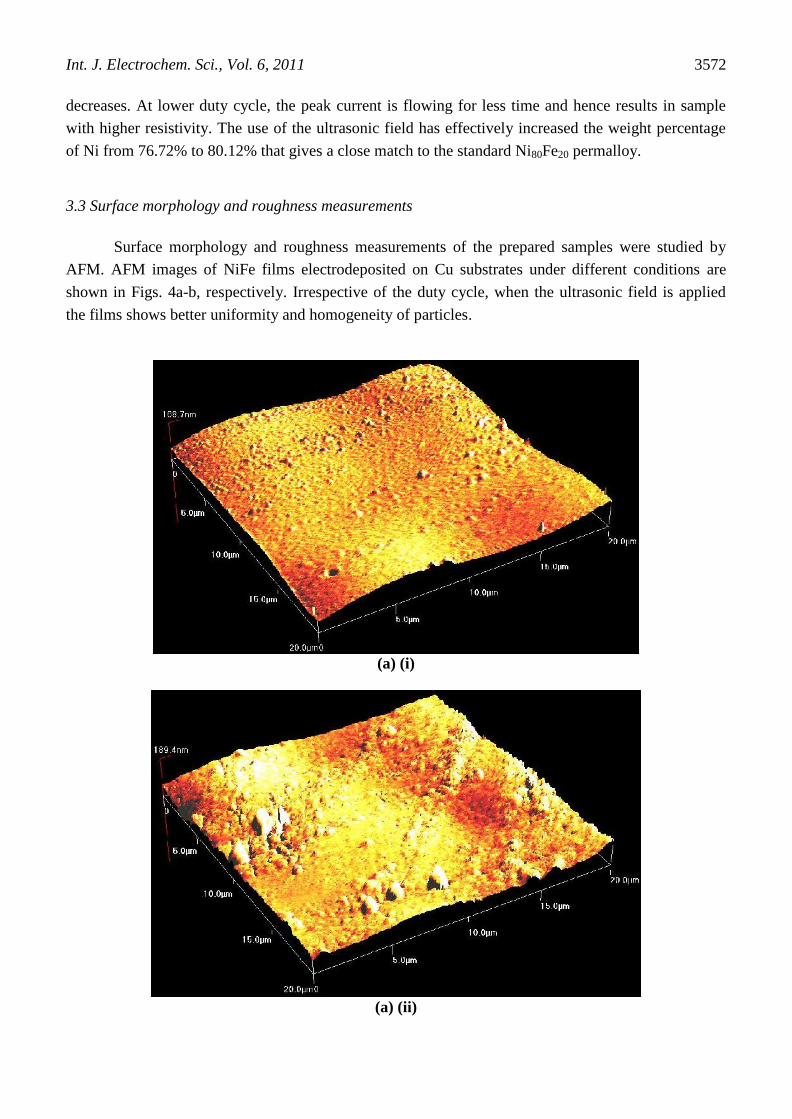
3.3 Surface morphology and roughness measurements
Surface morphology and roughness measurements of the prepared samples were studied by
AFM. AFM images of NiFe films electrodeposited on Cu substrates under different conditions are
shown in Figs. 4a-b, respectively. Irrespective of the duty cycle, when the ultrasonic field is applied
the films shows better uniformity and homogeneity of particles.
(a) (i)
(a) (ii)

Int. J. Electrochem. Sci., Vol. 6, 2011
3573
(b) (i)
(b) (ii)
Figure 4. AFM images of NiFe films electrodeposited on Cu substrates (a) without an ultrasonic field
for D (i) 50.00% (ii) 66.67% and (b) in the presence of an ultrasonic filed for d (i) 50.00% (ii)
66.67% for a current magnitude of 40 mA.
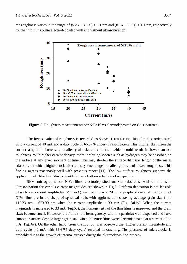
Fig. 5 shows the root-mean-square (RMS) roughness values for NiFe films electrodeposited on
Cu substrates under different conditions. In general, there is a trend of reduction in surface roughness
when there is an increase of current magnitude applied. The highest surface roughness of 39.01 nm,
measured at 20 mA without ultrasonic field condition is taken as reference. The surface roughness has
been reduced by 86% when the magnitude of applied current is increased from 20 mA to 40 mA,
irrespective of duty cycle and the ultrasonic field. When the duty cycle is decreased from 66.67 % to
50.00 %, there is a reduction of surface roughness to 75% irrespective of ultrasonic field and there is a
reduction of surface roughness from 80.67% to 70.8% when the external ultrasonic field is applied. It
is observed that as the current magnitude increases from 20 mA to 40 mA, the grain size decreases and
Int. J. Electrochem. Sci., Vol. 6, 2011
3574
the roughness varies in the range of (5.25 – 36.00) 1.1 nm and (8.16 – 39.01) 1.1 nm, respectively
for the thin films pulse electrodeposited with and without ultrasonication.
Figure 5. Roughness measurements for NiFe films electrodeposited on Cu substrates.
The lowest value of roughness is recorded as 5.251.1 nm for the thin film electrodeposited
with a current of 40 mA and a duty cycle of 66.67% under ultrasonication. This implies that when the
current amplitude increases, smaller grain sizes are formed which could result in lower surface
roughness. With higher current density, more inhibiting species such as hydrogen may be adsorbed on
the surface at any given moment of time. This may shorten the surface diffusion length of the metal
adatoms, in which higher nucleation density encourages smaller grains and lower roughness. This
finding agrees reasonably well with previous report [11]. The low surface roughness supports the
application of NiFe thin film to be utilized as a bottom substrate of a capacitor.
SEM micrographs for NiFe films electrodeposited on Cu substrates, without and with
ultrasonication for various current magnitudes are shown in Fig.6. Uniform deposition is not feasible
when lower current amplitudes (<40 mA) are used. The SEM micrographs show that the grains of
NiFe films are in the shape of spherical balls with agglomerations having average grain size from
112.23 nm – 623.30 nm when the current amplitude is 30 mA (Fig. 6ai-iv). When the current
magnitude is increased to 33 mA (Fig.6b), the homogeneity of the thin films is improved and the grain
sizes become small. However, the films show homogeneity, with the particles well dispersed and have
smoother surface despite larger grain size when the NiFe films were electrodeposited at a current of 35
mA (Fig. 6c). On the other hand, from the Fig. 6d, it is observed that higher current magnitude and
duty cycle (40 mA with 66.67% duty cycle) resulted in cracking. The presence of microcracks is
probably due to the growth of internal stresses during the electrodeposition process.

Int. J. Electrochem. Sci., Vol. 6, 2011
3575
(a)
(b)
(c)

Int. J. Electrochem. Sci., Vol. 6, 2011
3576
(d)
Figure 6. (a). SEM images of NiFe films electrodeposited on Cu substrates for 30 mA. (i) D = 50.00%
without ultrasonic field (ii) D = 50.00% in presence of ultrasonic field (iii) D = 66.67% without
ultrasonic field (iv) D = 66.67% in presence of ultrasonic field. (b) SEM images of NiFe films
electrodeposited on Cu substrates for 33 mA. (i) D = 50.00% without ultrasonic field (ii) D =
50.00% in presence of ultrasonic field (iii) D = 66.67% without ultrasonic field (iv) D =
66.67% in presence of ultrasonic field. (c) SEM images of NiFe films electrodeposited on Cu
substrates for 35 mA. (i) D = 50.00% without ultrasonic field (ii) D = 50.00% in presence of
ultrasonic field (iii) D = 66.67% without ultrasonic field (iv) D = 66.67% in presence of
ultrasonic field. (d) SEM images of NiFe films electrodeposited on Cu substrates for 40 mA
with D = 66.67% in presence of ultrasonic field.
Figure 7. Grain size analysis in NiFe films electrodeposited on Cu substrates.
Int. J. Electrochem. Sci., Vol. 6, 2011
3577
Fig.7 shows the range of grain sizes in NiFe films electrodeposited on Cu substrates without
and in the presence of an ultrasonic field for duty cycle of 50.00% and 66.67% at various current
magnitudes. It has been observed that when the current magnitude is increased, the grain sizes become
smaller and there is a reduction of grain size about by 10 times. When the duty cycle is decreased from
66.67 % to 50.00 %, the reduction in grain sizes is increased from 66 to 75% in the case of without
ultrasonic field and 61% to 74 % in the case of ultrasonic field. Hence, it has been deduced that the
current applied is the dominant factor in controlling the grain sizes, whereas the duty cycle and the
external ultrasonic field play secondary roles in the grain size reduction.
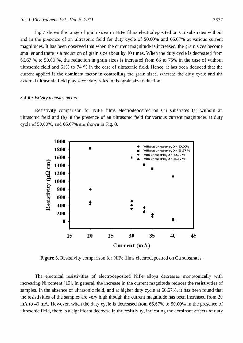
3.4 Resistivity measurements
Resistivity comparison for NiFe films electrodeposited on Cu substrates (a) without an
ultrasonic field and (b) in the presence of an ultrasonic field for various current magnitudes at duty
cycle of 50.00%, and 66.67% are shown in Fig. 8.
Figure 8. Resistivity comparison for NiFe films electrodeposited on Cu substrates.
The electrical resistivities of electrodeposited NiFe alloys decreases monotonically with
increasing Ni content [15]. In general, the increase in the current magnitude reduces the resistivities of
samples. In the absence of ultrasonic field, and at higher duty cycle at 66.67%, it has been found that
the resistivities of the samples are very high though the current magnitude has been increased from 20
mA to 40 mA. However, when the duty cycle is decreased from 66.67% to 50.00% in the presence of
ultrasonic field, there is a significant decrease in the resistivity, indicating the dominant effects of duty

Int. J. Electrochem. Sci., Vol. 6, 2011
3578
cycle and ultrasonic field. For example, when the current magnitude is lower and without application
of ultrasonic field, the deposited film exhibits resistivity of 1825.24 µcm, which is significantly
higher than that of thin film prepared at higher current magnitude. The observed higher electrical
resistivity of the electrodeposited alloys can be attributed to the smaller grain sizes, high defect
densities, and impurity incorporation during electrodeposition [15].
Figure 9. The relation between surface roughness and resistivity for samples measured in this study.
On the other hand, films deposited without the ultrasonic field have a relatively high resistivity
in spite of the larger grain size of the films which is due to the high surface roughness of the films. At
higher current magnitude applied, the ultrasonic field assisted in reducing unwanted sediments in the
electrolyte from being electrodeposited onto the substrate, and inducing rapid crystallization of the
NiFe materials to form nanoparticles [2]. Thus, the optimum deposition condition is found to be at a
current of 40 mA and a duty cycle of 50.00 % in the presence of ultrasonic field with the deposited
film exhibits the lowest resistivity at 19.86 µcm.
Fig. 9 shows the relation between surface roughness and resistivity. The change of resistivity
appeared to be approximately linear with surface roughness when the ultrasonic field is applied but
appeared to exponentially increasing with surface roughness when there is no ultrasonic field. The
lowest value of resistivity obtained is comparable to the previous report [9].
4. CONCLUSIONS
NiFe films were pulse electrodeposited on conductive copper substrates under galvanostatic
mode with and without ultrasonication for different pulse current magnitudes and duty cycles. The
Int. J. Electrochem. Sci., Vol. 6, 2011
3579
optimum deposition conditions are found to be at a deposition current of 40 mA and a duty cycle of
50.00% with ultrasonic treatment. A close match to the Ni80Fe20 permalloy film is achieved with the
NiFe film having significantly smaller grain size and reduced surface roughness. The NiFe films are
highly textured having a (2 2 0) preferred orientation. Through the optimization study, the deposition
current is observed to be the dominant factor in determining the single phase deposition of NiFe film
whereas the ultrasonic field and the duty cycle significantly reduce the surface roughness and the
spherical grain size, all of which combine to reduce film resistivity.
ACKNOWLEDGEMENTS
The authors are grateful to the Ministry of Science, Technology and Innovation (MOSTI), Malaysia
for supporting their work under eScience fund (Project No. 03-02-01-SF0059) as well as Mr Ho Soon
Min, Mr Kelvin Koh, Mr Hoon Jian Wei and Mr Pachamuthu for their assistance with the
characterizations.
References
1. W. Tang, K. Xu, P. Wang, X. Li, Microelectron. Eng. 66 (2003) 445.
2. D. H. Kim, H. W. Ryu, J. H. Moon, J. Kim, J. Power Sources 163 (2006) 196.
3. L. J. Gao, P. Ma, K. M. Novogradecz, P. R. Norton, J. Appl. Phys. 81 (1997) 7595.
4. R. Balachandran, H. K. Yow, B. H. Ong, R. Manickam, V. Saaminathan, K. B. Tan, J. Alloys
Compd. 481 (2009) 336.
5. S. Uchida, J. Xue, B. P. Rand, S. R. Forrest, Appl. Phys. Lett. 84 (2004) 4218.
6. P. B. S. N. V. Prasad, R. Vasudevan, S. K. Seshadri, S. Ahila, Mater. Lett. 17 (1993) 357.
7. K. H. Ahn, S. Baik, S. S. Kim, J. Appl. Phys. 92 (2002) 2651.
8. A.M. Nguyen, S. Cercelaru, G. Tremblay, J. C. Perron, P. Hesto, Thin Solid Films 275 (1996) 231.
9. C. Nishimura, Y. Nagai, K. Yanagisawa, T. Toshima, Magnetics, IEEE Transactions , 23 (1987)
2728.
10. M. Bedir, O. Bakkaloğlu, I. Karahan, M. Öztaş, Pramana, 66 (2006) 1093.
11. I.Tabakovic, S. Riemer, V. Vas'ko, V. Sapozhnikov, M. Kief, J. Electrochem. Soc. 150 (2003)
C635.
12. A.-E. M. M. Urse, M. Grigoras, H. Chiriac, J. Optoelectron. Adv. M. 7 (2005) 759.
13. L. Chih-Huang, H. Matsuyama, R. L. White, T. C. Anthony, Magnetics, IEEE Transactions on, 31
(1995) 2609.
14. T. Nakanishi, M. Ozaki, H.-S. Nam, T. Yokoshima, T. Osaka, J. Electrochem. Soc. 148 (2001)
C627.
15. N. V. Myung, D. Y. Park, B. Y. Yoo, P. T. A. Sumodjo, J. Magn. Magn. Mater. 265 (2003) 189.
© 2011 by ESG (www.electrochemsci.org)