Embed Size (px)
Citation preview
© KEMET Electronics Corporation • P.O. Box 5928 • Greenville, SC 29606 • 864-963-6300 • www.kemet.com C1023_X7R_AUTO_SMD • 4/26/2018 1One world. One KEMET
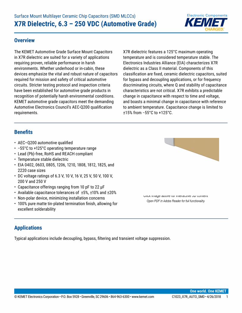
Benefits
• AEC–Q200automotivequalified• −55°Cto+125°Coperatingtemperaturerange• Lead(Pb)-free,RoHSandREACHcompliant• Temperaturestabledielectric• EIA0402,0603,0805,1206,1210,1808,1812,1825,and
2220 case sizes• DCvoltageratingsof6.3V,10V,16V,25V,50V,100V,200Vand250V
• Capacitanceofferingsrangingfrom10pFto22μF• Availablecapacitancetolerancesof±5%,±10%and±20%• Non-polardevice,minimizinginstallationconcerns• 100%puremattetin-platedterminationfinish,allowingforexcellentsolderability
Overview
TheKEMETAutomotiveGradeSurfaceMountCapacitorsinX7Rdielectricaresuitedforavarietyofapplicationsrequiringproven,reliableperformanceinharshenvironments.Whetherunderhoodorin-cabin,thesedevicesemphasizethevitalandrobustnatureofcapacitorsrequiredformissionandsafetyofcriticalautomotivecircuits.Strictertestingprotocolandinspectioncriteriahavebeenestablishedforautomotivegradeproductsinrecognitionofpotentiallyharshenvironmentalconditions.KEMETautomotivegradecapacitorsmeetthedemandingAutomotiveElectronicsCouncil'sAEC-Q200qualificationrequirements.
X7Rdielectricfeaturesa125°Cmaximumoperatingtemperatureandisconsideredtemperaturestable.TheElectronicsIndustriesAlliance(EIA)characterizesX7RdielectricasaClassIImaterial.Componentsofthisclassificationarefixed,ceramicdielectriccapacitors,suitedforbypassanddecouplingapplications,orforfrequencydiscriminatingcircuits,whereQandstabilityofcapacitancecharacteristicsarenotcritical.X7Rexhibitsapredictablechangeincapacitancewithrespecttotimeandvoltage,andboastsaminimalchangeincapacitancewithreferencetoambienttemperature.Capacitancechangeislimitedto±15%from−55°Cto+125°C.
SurfaceMountMultilayerCeramicChipCapacitors(SMDMLCCs)
X7R Dielectric, 6.3 – 250 VDC (Automotive Grade)
Applications
Typicalapplicationsincludedecoupling,bypass,filteringandtransientvoltagesuppression.
© KEMET Electronics Corporation • P.O. Box 5928 • Greenville, SC 29606 • 864-963-6300 • www.kemet.com C1023_X7R_AUTO_SMD • 4/26/2018 2
Surface Mount Multilayer Ceramic Chip Capacitors (SMD MLCCs) X7R Dielectric, 6.3 – 250 VDC (Automotive Grade)
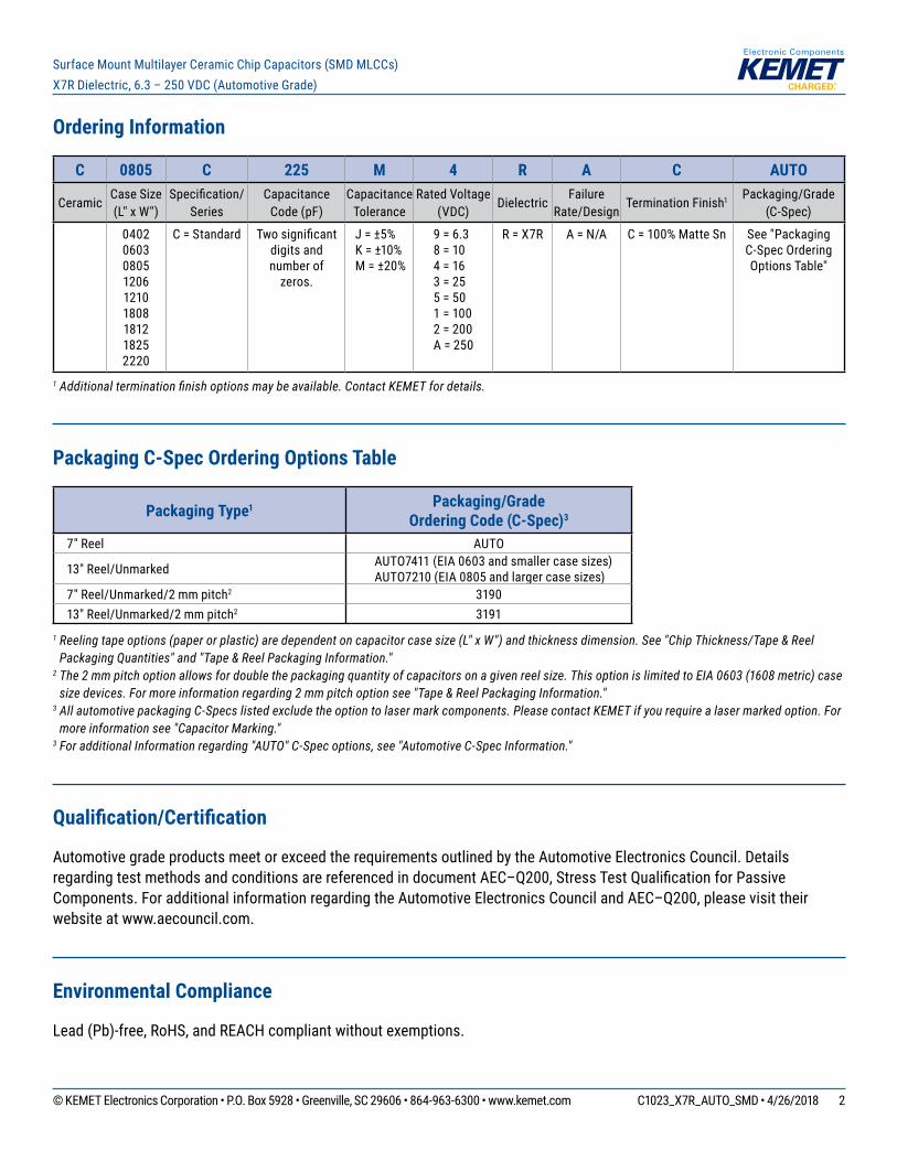
Ordering Information
C 0805 C 225 M 4 R A C AUTO
CeramicCase Size (L"xW")
Specification/Series
Capacitance Code(pF)
Capacitance Tolerance
RatedVoltage(VDC)
DielectricFailure
Rate/DesignTerminationFinish1 Packaging/Grade
(C-Spec)
040206030805120612101808181218252220
C=Standard Twosignificantdigitsandnumberof
zeros.
J=±5%K=±10%M=±20%
9 = 6.38 = 104 = 163 = 255 = 501 = 1002 = 200A = 250
R = X7R A = N/A C=100%MatteSn See"PackagingC-SpecOrderingOptionsTable"
1 Additional termination finish options may be available. Contact KEMET for details.
Packaging C-Spec Ordering Options Table
Packaging Type1 Packaging/Grade Ordering Code (C-Spec)3
7"Reel AUTO
13"Reel/Unmarked AUTO7411(EIA0603andsmallercasesizes)AUTO7210(EIA0805andlargercasesizes)
7"Reel/Unmarked/2mmpitch2 319013"Reel/Unmarked/2mmpitch2 3191
1 Reeling tape options (paper or plastic) are dependent on capacitor case size (L" x W") and thickness dimension. See "Chip Thickness/Tape & Reel Packaging Quantities" and "Tape & Reel Packaging Information."
2 The 2 mm pitch option allows for double the packaging quantity of capacitors on a given reel size. This option is limited to EIA 0603 (1608 metric) case size devices. For more information regarding 2 mm pitch option see "Tape & Reel Packaging Information."
3 All automotive packaging C-Specs listed exclude the option to laser mark components. Please contact KEMET if you require a laser marked option. For more information see "Capacitor Marking."
3 For additional Information regarding "AUTO" C-Spec options, see "Automotive C-Spec Information."
Qualification/Certification
AutomotivegradeproductsmeetorexceedtherequirementsoutlinedbytheAutomotiveElectronicsCouncil.DetailsregardingtestmethodsandconditionsarereferencedindocumentAEC–Q200,StressTestQualificationforPassiveComponents.ForadditionalinformationregardingtheAutomotiveElectronicsCouncilandAEC–Q200,pleasevisittheirwebsiteatwww.aecouncil.com.
Environmental Compliance
Lead(Pb)-free,RoHS,andREACHcompliantwithoutexemptions.
© KEMET Electronics Corporation • P.O. Box 5928 • Greenville, SC 29606 • 864-963-6300 • www.kemet.com C1023_X7R_AUTO_SMD • 4/26/2018 3
Surface Mount Multilayer Ceramic Chip Capacitors (SMD MLCCs) X7R Dielectric, 6.3 – 250 VDC (Automotive Grade)
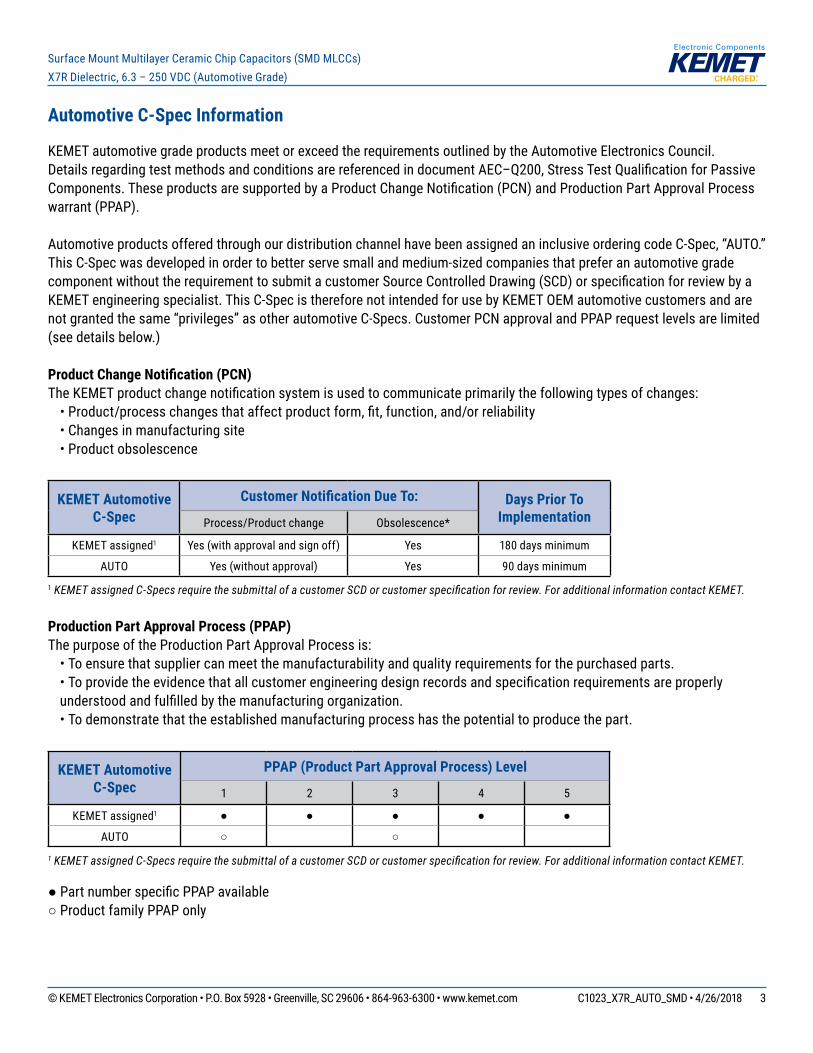
Automotive C-Spec Information
KEMETautomotivegradeproductsmeetorexceedtherequirementsoutlinedbytheAutomotiveElectronicsCouncil.DetailsregardingtestmethodsandconditionsarereferencedindocumentAEC–Q200,StressTestQualificationforPassiveComponents.TheseproductsaresupportedbyaProductChangeNotification(PCN)andProductionPartApprovalProcesswarrant(PPAP).
AutomotiveproductsofferedthroughourdistributionchannelhavebeenassignedaninclusiveorderingcodeC-Spec,“AUTO.”ThisC-Specwasdevelopedinordertobetterservesmallandmedium-sizedcompaniesthatpreferanautomotivegradecomponentwithouttherequirementtosubmitacustomerSourceControlledDrawing(SCD)orspecificationforreviewbyaKEMETengineeringspecialist.ThisC-SpecisthereforenotintendedforusebyKEMETOEMautomotivecustomersandarenotgrantedthesame“privileges”asotherautomotiveC-Specs.CustomerPCNapprovalandPPAPrequestlevelsarelimited(seedetailsbelow.)
Product Change Notifi cation (PCN)TheKEMETproductchangenotificationsystemisusedtocommunicateprimarilythefollowingtypesofchanges: •Product/processchangesthataffectproductform,fit,function,and/orreliability •Changesinmanufacturingsite •Productobsolescence
KEMET Automotive C-Spec
Customer Notifi cation Due To: Days Prior To ImplementationProcess/Productchange Obsolescence*
KEMETassigned1 Yes(withapprovalandsignoff) Yes 180daysminimum
AUTO Yes(withoutapproval) Yes 90daysminimum1 KEMET assigned C-Specs require the submittal of a customer SCD or customer specifi cation for review. For additional information contact KEMET.
Production Part Approval Process (PPAP)ThepurposeoftheProductionPartApprovalProcessis: •Toensurethatsuppliercanmeetthemanufacturabilityandqualityrequirementsforthepurchasedparts. •Toprovidetheevidencethatallcustomerengineeringdesignrecordsandspecificationrequirementsareproperlyunderstoodandfulfilledbythemanufacturingorganization.
•Todemonstratethattheestablishedmanufacturingprocesshasthepotentialtoproducethepart.
KEMET Automotive C-Spec
PPAP (Product Part Approval Process) Level
1 2 3 4 5
KEMETassigned1 ● ● ● ● ●
AUTO ○ ○1 KEMET assigned C-Specs require the submittal of a customer SCD or customer specifi cation for review. For additional information contact KEMET.
●PartnumberspecificPPAPavailable○ProductfamilyPPAPonly
© KEMET Electronics Corporation • P.O. Box 5928 • Greenville, SC 29606 • 864-963-6300 • www.kemet.com C1023_X7R_AUTO_SMD • 4/26/2018 4
Surface Mount Multilayer Ceramic Chip Capacitors (SMD MLCCs) X7R Dielectric, 6.3 – 250 VDC (Automotive Grade)
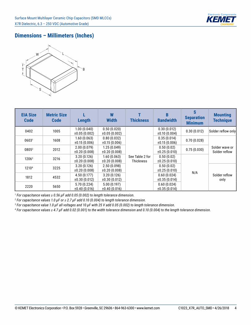
Dimensions – Millimeters (Inches)
L
B
W
S
T
EIA Size Code
Metric Size Code
L Length
W Width
T Thickness
B Bandwidth
SSeparation Minimum
Mounting Technique
0402 1005 1.00(0.040) ±0.05(0.002)
0.50(0.020) ±0.05(0.002)
SeeTable2forThickness
0.30(0.012) ±0.10(0.004) 0.30(0.012) Solderreflowonly
06031 1608 1.60(0.063) ±0.15(0.006)
0.80(0.032) ±0.15(0.006)
0.35(0.014) ±0.15(0.006) 0.70(0.028)
SolderwaveorSolderreflow08052 2012 2.00(0.079)
±0.20(0.008)1.25(0.049) ±0.20(0.008)
0.50(0.02) ±0.25(0.010) 0.75(0.030)
12063 3216 3.20(0.126) ±0.20(0.008)
1.60(0.063) ±0.20(0.008)
0.50(0.02) ±0.25(0.010)
N/A12104 3225 3.20(0.126)
±0.20(0.008)2.50(0.098) ±0.20(0.008)
0.50(0.02) ±0.25(0.010)
Solderreflowonly1812 4532 4.50(0.177)
±0.30(0.012)3.20(0.126) ±0.30(0.012)
0.60(0.024) ±0.35(0.014)
2220 5650 5.70(0.224) ±0.40(0.016)
5.00(0.197) ±0.40(0.016)
0.60(0.024) ±0.35(0.014)
1 For capacitance values ≥ 0.56 µF add 0.05 (0.002) to length tolerance dimension.2 For capacitance values 1.0 µF or ≥ 2.7 µF add 0.10 (0.004) to length tolerance dimension.3 For capacitance value 1.0 µF all voltages and 10 µF with 25 V add 0.05 (0.002) to length tolerance dimension.4 For capacitance values ≥ 4.7 µF add 0.02 (0.001) to the width tolerance dimension and 0.10 (0.004) to the length tolerance dimension.
© KEMET Electronics Corporation • P.O. Box 5928 • Greenville, SC 29606 • 864-963-6300 • www.kemet.com C1023_X7R_AUTO_SMD • 4/26/2018 5
Surface Mount Multilayer Ceramic Chip Capacitors (SMD MLCCs) X7R Dielectric, 6.3 – 250 VDC (Automotive Grade)
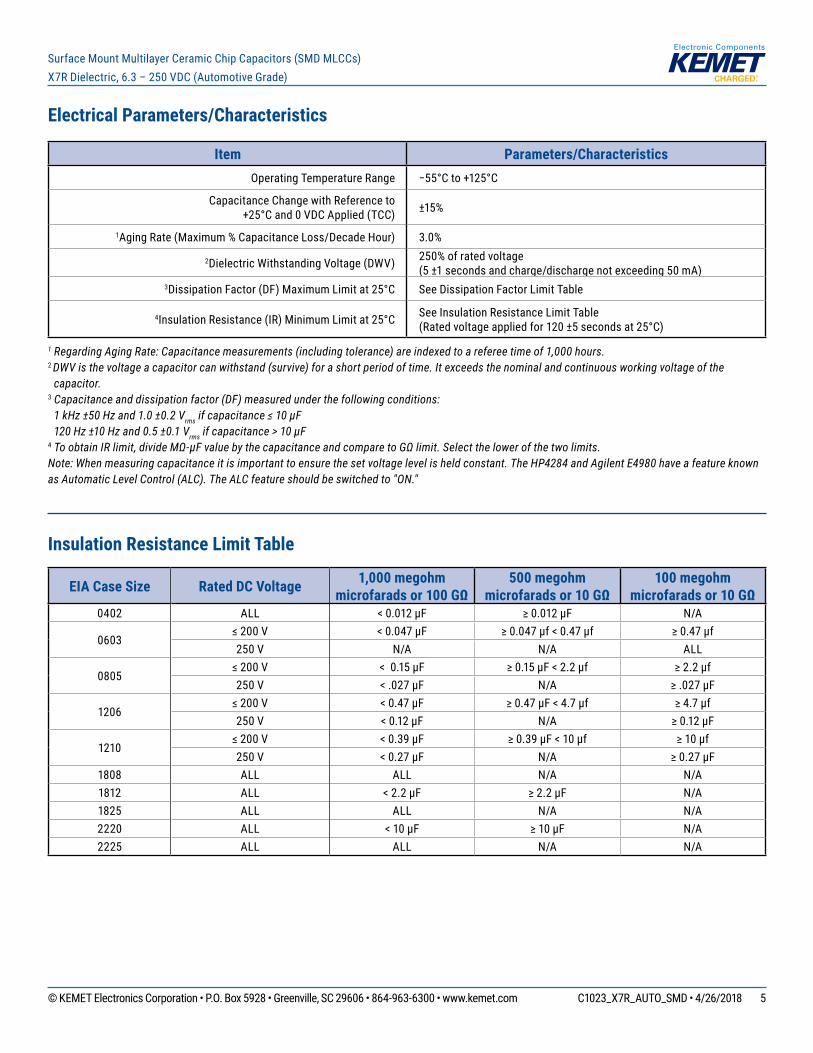
Electrical Parameters/Characteristics
Item Parameters/CharacteristicsOperatingTemperatureRange −55°Cto+125°C
CapacitanceChangewithReferenceto +25°Cand0VDCApplied(TCC) ±15%
1AgingRate(Maximum%CapacitanceLoss/DecadeHour) 3.0%
2DielectricWithstandingVoltage(DWV) 250%ofratedvoltage (5±1secondsandcharge/dischargenotexceeding50mA)
3DissipationFactor(DF)MaximumLimitat25°C SeeDissipationFactorLimitTable
4InsulationResistance(IR)MinimumLimitat25°C SeeInsulationResistanceLimitTable (Ratedvoltageappliedfor120±5secondsat25°C)
1 Regarding Aging Rate: Capacitance measurements (including tolerance) are indexed to a referee time of 1,000 hours.2 DWV is the voltage a capacitor can withstand (survive) for a short period of time. It exceeds the nominal and continuous working voltage of the
capacitor.3 Capacitance and dissipation factor (DF) measured under the following conditions: 1 kHz ±50 Hz and 1.0 ±0.2 Vrms if capacitance ≤ 10 µF 120 Hz ±10 Hz and 0.5 ±0.1 Vrms if capacitance > 10 µF4 To obtain IR limit, divide MΩ-µF value by the capacitance and compare to GΩ limit. Select the lower of the two limits.Note: When measuring capacitance it is important to ensure the set voltage level is held constant. The HP4284 and Agilent E4980 have a feature known as Automatic Level Control (ALC). The ALC feature should be switched to "ON."
Insulation Resistance Limit Table
EIA Case Size Rated DC Voltage 1,000 megohm microfarads or 100 GΩ
500 megohm microfarads or 10 GΩ
100 megohm microfarads or 10 GΩ
0402 ALL <0.012µF ≥0.012µF N/A
0603≤200V <0.047µF ≥0.047µf<0.47µf ≥0.47µf250V N/A N/A ALL
0805≤200V <0.15µF ≥0.15µF<2.2µf ≥2.2µf250V <.027µF N/A ≥.027µF
1206≤200V <0.47µF ≥0.47µF<4.7µf ≥4.7µf250V <0.12µF N/A ≥0.12µF
1210≤200V <0.39µF ≥0.39µF<10µf ≥10µf250V <0.27µF N/A ≥0.27µF
1808 ALL ALL N/A N/A1812 ALL <2.2µF ≥2.2µF N/A1825 ALL ALL N/A N/A2220 ALL <10µF ≥10µF N/A2225 ALL ALL N/A N/A
© KEMET Electronics Corporation • P.O. Box 5928 • Greenville, SC 29606 • 864-963-6300 • www.kemet.com C1023_X7R_AUTO_SMD • 4/26/2018 6
Surface Mount Multilayer Ceramic Chip Capacitors (SMD MLCCs) X7R Dielectric, 6.3 – 250 VDC (Automotive Grade)
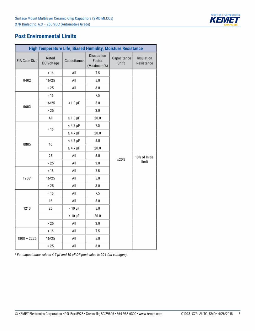
Post Environmental Limits
High Temperature Life, Biased Humidity, Moisture Resistance
EIA Case SizeRated
DCVoltageCapacitance
Dissipation Factor
(Maximum%)
Capacitance Shift
Insulation Resistance
0402
< 16 All 7.5
±20% 10%ofInitiallimit
16/25 All 5.0
> 25 All 3.0
0603
< 16
<1.0µF
7.5
16/25 5.0
> 25 3.0
All ≥1.0µF 20.0
0805
< 16<4.7µF 7.5
≥4.7µF 20.0
16<4.7µF 5.0
≥4.7µF 20.0
25 All 5.0
> 25 All 3.0
12061
< 16 All 7.5
16/25 All 5.0
> 25 All 3.0
1210
< 16 All 7.5
16 All 5.0
25 <10µF 5.0
≥10µF 20.0
> 25 All 3.0
1808 – 2225
< 16 All 7.5
16/25 All 5.0
> 25 All 3.0
1 For capacitance values 4.7 µf and 10 µF DF post value is 20% (all voltages).
© KEMET Electronics Corporation • P.O. Box 5928 • Greenville, SC 29606 • 864-963-6300 • www.kemet.com C1023_X7R_AUTO_SMD • 4/26/2018 7
Surface Mount Multilayer Ceramic Chip Capacitors (SMD MLCCs) X7R Dielectric, 6.3 – 250 VDC (Automotive Grade)
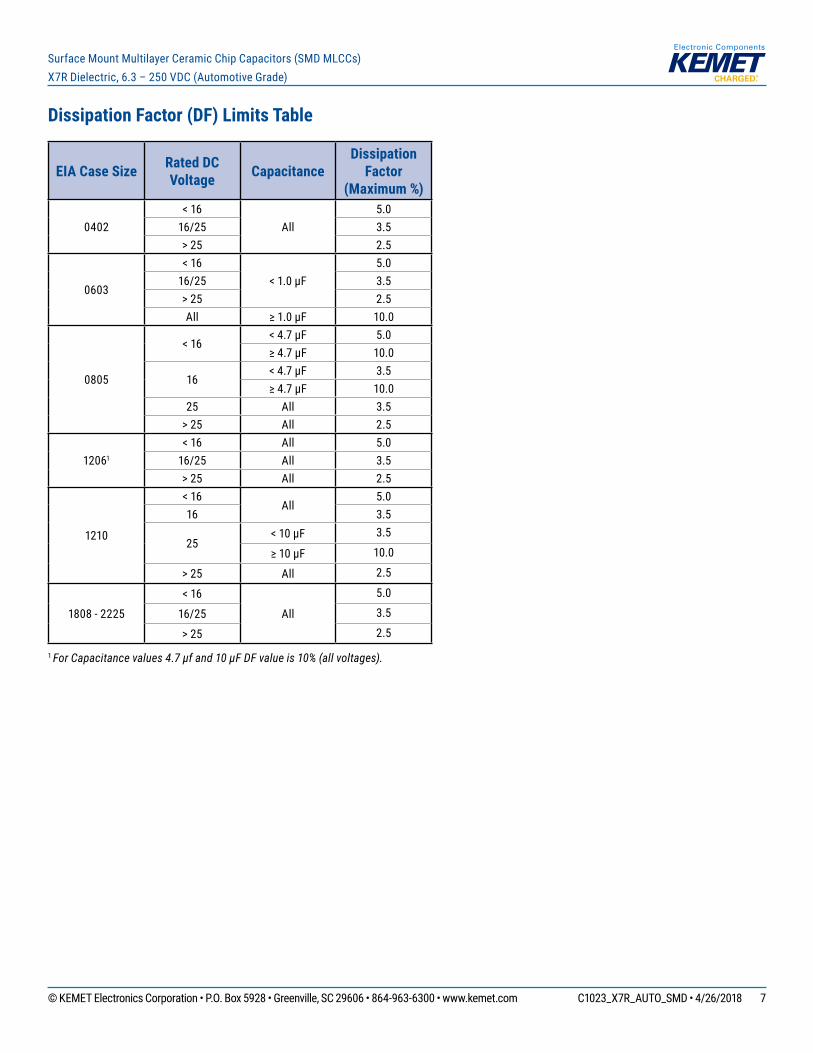
Dissipation Factor (DF) Limits Table
EIA Case Size Rated DC Voltage Capacitance
Dissipation Factor
(Maximum %)
0402< 16
All5.0
16/25 3.5> 25 2.5
0603
< 16<1.0µF
5.016/25 3.5> 25 2.5All ≥1.0µF 10.0
0805
< 16<4.7µF 5.0≥4.7µF 10.0
16<4.7µF 3.5≥4.7µF 10.0
25 All 3.5> 25 All 2.5
12061
< 16 All 5.016/25 All 3.5> 25 All 2.5
1210
< 16All
5.016 3.5
25<10µF 3.5
≥10µF 10.0
> 25 All 2.5
1808 - 2225
< 16
All
5.0
16/25 3.5
> 25 2.5
1 For Capacitance values 4.7 µf and 10 µF DF value is 10% (all voltages).
© KEMET Electronics Corporation • P.O. Box 5928 • Greenville, SC 29606 • 864-963-6300 • www.kemet.com C1023_X7R_AUTO_SMD • 4/26/2018 8
Surface Mount Multilayer Ceramic Chip Capacitors (SMD MLCCs) X7R Dielectric, 6.3 – 250 VDC (Automotive Grade)
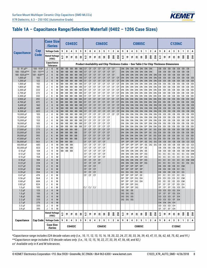
Table 1A – Capacitance Range/Selection Waterfall (0402 – 1206 Case Sizes)
*Capacitance range includes E24 decade values only (i.e., 10, 11, 12, 13, 15, 16, 18, 20, 22, 24, 27, 30, 33, 36, 39, 43, 47, 51, 56, 62, 68, 75, 82, and 91.)**Capacitance range includes E12 decade values only. (i.e., 10, 12, 15, 18, 22, 27, 33, 39, 47, 56, 68, and 82.)xx1 Available only in K and M tolerances.
Capacitance Cap Code
Case Size /Series C0402C C0603C C0805C C1206C
Voltage Code 9 8 4 3 5 9 8 4 3 5 1 2 A 9 8 4 3 5 1 2 A 9 8 4 3 5 1 2 A
Rated Voltage (VDC) 6.
3 10 16 25 50 6.3 10 16 25 50 100
200
250
6.3 10 16 25 50 100
200
250
6.3 10 16 25 50 100
200
250
Capacitance Tolerance Product Availability and Chip Thickness Codes – See Table 2 for Chip Thickness Dimensions
10-91pF* 100-910* J K M BB BB BB BB BB CF CF CF CF CF CF CF DN DN DN DN DN DN DN EB EB EB EB EB EB EB100-150pF** 101-151** J K M BB BB BB BB BB CF CF CF CF CF CF CF DN DN DN DN DN DN DN EB EB EB EB EB EB EB180-820pF** 181-820** J K M BB BB BB BB BB CF CF CF CF CF CF CF DN DN DN DN DN DN DN DN EB EB EB EB EB EB EB
1,000pF 102 J K M BB BB BB BB BB CF CF CF CF CF CF CF CF DN DN DN DN DN DN DN DN EB EB EB EB EB EB EB EB1,200pF 122 J K M BB BB BB BB BB CF CF CF CF CF CF CF CF DN DN DN DN DN DN DN DN EB EB EB EB EB EB EB EB1,500pF 152 J K M BB BB BB BB BB CF CF CF CF CF CF CF CF DN DN DN DN DN DN DN DN EB EB EB EB EB EB EB EB1,800pF 182 J K M BB BB BB BB BB CF CF CF CF CF CF CF CF DN DN DN DN DN DN DN DN EB EB EB EB EB EB EB EB2,200pF 222 J K M BB BB BB BB BB CF CF CF CF CF CF CF CF DN DN DN DN DN DN DN DN EB EB EB EB EB EB EB EB2,700pF 272 J K M BB BB BB BB BB CF CF CF CF CF CF CF CF DN DN DN DN DN DN DN DN EB EB EB EB EB EB EB EB3,300pF 332 J K M BB BB BB BB BB CF CF CF CF CF CF CF CF DN DN DN DN DN DN DN DN EB EB EB EB EB EB EB EB3,900pF 392 J K M BB BB BB BB BB CF CF CF CF CF CF CF CF DN DN DN DN DN DN DN DN EB EB EB EB EB EB EB EB4,700pF 472 J K M BB BB BB BB BB CF CF CF CF CF CF CF CF DN DN DN DN DN DN DN DN EB EB EB EB EB EB EB EB5,600pF 562 J K M BB BB BB BB BB CF CF CF CF CF CF CF CF DN DN DN DN DN DN DN DN EB EB EB EB EB EB EB EB6,800pF 682 J K M BB BB BB BB BB CF CF CF CF CF CF CF CF DN DN DN DN DN DN DN DN EB EB EB EB EB EB EB EB8,200pF 822 J K M BB BB BB BB BB CF CF CF CF CF CF CF CF DN DN DN DN DN DN DN DN EB EB EB EB EB EB EB EB10,000pF 103 J K M BB BB BB BB BB CF CF CF CF CF CF CF CF DN DN DN DN DN DN DN DN EB EB EB EB EB EB EB EB12,000pF 123 J K M BB BB BB BB BB CF CF CF CF CF CF DN DN DN DN DN DN DN DN EB EB EB EB EB EB EB EB15,000pF 153 J K M BB BB BB BB BB CF CF CF CF CF CF DN DN DN DN DN DP DN DN EB EB EB EB EB EB EB EB18,000pF 183 J K M BB BB BB BB BB CF CF CF CF CF CF DN DN DN DN DN DP DN DN EB EB EB EB EB EB EB EB22,000pF 223 J K M BB BB BB BB BB CF CF CF CF CF CF DN DN DN DN DN DP DN DN EB EB EB EB EB EB EB EB27,000pF 273 J K M BB BB BB BB CF CF CF CF CF CF DN DN DN DN DN DP DE DG EB EB EB EB EB EB EB EB33,000pF 333 J K M BB BB BB BB CF CF CF CF CF CF DN DN DN DN DN DP DE DG EB EB EB EB EB EB EB EB39,000pF 393 J K M BB BB BB BB CF CF CF CF CF CF DN DN DN DN DN DP DE DG EB EB EB EB EB EC EB EB47,000pF 473 J K M BB BB BB BB CF CF CF CF CF CF DN DN DN DN DN DE DG DG EB EB EB EB EB EC ED ED56,000pF 563 J K M BB BB BB CF CF CF CF CF DP DP DP DP DP DE DG DG EB EB EB EB EB EB ED ED68,000pF 683 J K M BB BB BB CF CF CF CF CF DP DP DP DP DP DE DG DG EB EB EB EB EB EB ED ED82,000pF 823 J K M BB BB BB CF CF CF CF CF DP DP DP DP DP DE EB EB EB EB EB EB ED ED0.10µF 104 J K M BB BB BB CF CF CF CF CF DN DN DN DN DN DE EB EB EB EB EB EB EM EM0.12µF 124 J K M CF CF CF CF CF DN DN DN DN DP DG EC EC EC EC EC EC EG EM0.15µF 154 J K M CF CF CF CF CF DN DN DN DN DP DG EC EC EC EC EC EC EG EG0.18µF 184 J K M CF CF CF CF DN DN DN DN DP DG EC EC EC EC EC EC EM EM0.22µF 224 J K M CF CF CF CF DN DN DN DN DP DG EC EC EC EC EC EC EG EG0.27µF 274 J K M CF CF CF DP DP DP DP DP EB EB EB EB EC EM0.33µF 334 J K M CF CF CF DP DP DP DP DP EB EB EB EB EC EG0.39µF 394 J K M CF CF CF DG DG DG DG DE EB EB EB EB EC EG0.47µF 474 J K M CF CF CF DP DP DP DP DE EC EC EC EC EC EG0.56µF 564 J K M DP DP DP DG DH ED ED ED ED EC EM0.68µF 684 J K M DP DP DP DG DH EE EE EE EE ED EM0.82µF 824 J K M DP DP DP DG EF EF EF EF ED EH1.0µF 105 J K M CJ ¹ CJ¹ CJ¹ DP DP DP DG EF EF EF EG ED EH1.2µF 125 J K M DE DE DE ED ED ED EG EH1.5µF 155 J K M DG DG DG EF EF EF EG EH1.8µF 185 J K M DG DG DG ED ED ED EF EH2.2µF 225 J K M DG DG DG ED ED ED EF EH2.7µF 275 J K M EN EN EN EH3.3µF 335 J K M ED ED ED EH3.9µF 395 J K M EF EF EF EH
Capacitance Cap Code
Rated Voltage (VDC) 6.
3 10 16 25 50 6.3 10 16 25 50 100
200
250
6.3 10 16 25 50 100
200
250
6.3 10 16 25 50 100
200
250
Voltage Code 9 8 4 3 5 9 8 4 3 5 1 2 A 9 8 4 3 5 1 2 A 9 8 4 3 5 1 2 A
Case Size/Series C0402C C0603C C0805C C1206C
© KEMET Electronics Corporation • P.O. Box 5928 • Greenville, SC 29606 • 864-963-6300 • www.kemet.com C1023_X7R_AUTO_SMD • 4/26/2018 9
Surface Mount Multilayer Ceramic Chip Capacitors (SMD MLCCs) X7R Dielectric, 6.3 – 250 VDC (Automotive Grade)
Table 1B – Capacitance Range/Selection Waterfall (1210 – 2220 Case Sizes)
*Capacitance range Includes E24 decade values only. (i.e., 10, 11, 12, 13, 15, 16, 18, 20, 22, 24, 27, 30, 33, 36, 39, 43, 47, 51, 56, 62, 68, 75, 82 and 91)**Capacitance range Includes E12 decade values only. (i.e., 10, 12, 15, 18, 22, 27, 33, 39, 47, 56, 68 and 82)
Capacitance Cap Code
Case Size/Series C1210C C1808C C1812C C1825C C2220C
Voltage Code 9 8 4 3 5 1 2 A 5 1 2 3 5 1 2 A 5 1 2 A 3 5 1 2 A
Rated Voltage (VDC) 6.
3 10 16 25 50 100
200
250
50 100
200
25 50 100
200
250
50 100
200
250
25 50 100
200
250
Capacitance Tolerance Product Availability and Chip Thickness Codes – See Table 2 for Chip Thickness Dimensions
10-91pF* 100-910* J K M FB FB FB FB FB FB FB100-270pF** 101-271** J K M FB FB FB FB FB FB FB
330pF 331 J K M FB FB FB FB FB FB FB LF LF LF390pF 391 J K M FB FB FB FB FB FB FB LF LF LF
470-820pF** 471-821** J K M FB FB FB FB FB FB FB LF LF LF GB GB GB GB1,000pF 102 J K M FB FB FB FB FB FB FB LF LF LF GB GB GB GB1,200pF 122 J K M FB FB FB FB FB FB FB LF LF LF GB GB GB GB1,500pF 152 J K M FB FB FB FB FB FB FE LF LF LF GB GB GB GB1,800pF 182 J K M FB FB FB FB FB FB FE LF LF LF GB GB GB GB2,200pF 222 J K M FB FB FB FB FB FB FB FB LF LF LF GB GB GB GB2,700pF 272 J K M FB FB FB FB FB FB FB FB LF LF LF GB GB GB GB3,300pF 332 J K M FB FB FB FB FB FB FB FB LF LF GB GB GB GB3,900pF 392 J K M FB FB FB FB FB FB FB FB LF LF GB GB GB GB4,700pF 472 J K M FB FB FB FB FB FB FB FB LD LD GB GB GB GD5,600pF 562 J K M FB FB FB FB FB FB FB FB LD LD GB GB GB GH6,800pF 682 J K M FB FB FB FB FB FB FB FB LD LD GB GB GB GB GB JE JE8,200pF 822 J K M FB FB FB FB FB FB FB FB LD LD GB GB GB GB GB JE JE10,000pF 103 J K M FB FB FB FB FB FB FB FB LD LD GB GB GB GB GB JE JE12,000pF 123 J K M FB FB FB FB FB FB FB FB LD LD GB GB GB GB GB JE JE15,000pF 153 J K M FB FB FB FB FB FB FB FB LD LD GB GB GB GB GB JE JE
Capacitance Cap Code
Rated Voltage (VDC) 6.
3 10 16 25 50 100
200
250
50 100
200
25 50 100
200
250
50 100
200
250
25 50 100
200
250
Voltage Code 9 8 4 3 5 1 2 A 5 1 2 3 5 1 2 A 5 1 2 A 3 5 1 2 A
Case Size /Series C1210C C1808C C1812C C1825C C2220C
Table 1A – Capacitance Range/Selection Waterfall (0402 – 1206 Case Sizes) cont'd
*Capacitance range Includes E24 decade values only. (i.e., 10, 11, 12, 13, 15, 16, 18, 20, 22, 24, 27, 30, 33, 36, 39, 43, 47, 51, 56, 62, 68, 75, 82 and 91)**Capacitance range Includes E12 decade values only. (i.e., 10, 12, 15, 18, 22, 27, 33, 39, 47, 56, 68 and 82)xx¹ Available only in K andM tolerance.
Capacitance Cap Code
Case Size /Series C0402C C0603C C0805C C1206C
Voltage Code 9 8 4 3 5 9 8 4 3 5 1 2 A 9 8 4 3 5 1 2 A 9 8 4 3 5 1 2 A
Rated Voltage (VDC) 6.
3 10 16 25 50 6.3 10 16 25 50 100
200
250
6.3 10 16 25 50 100
200
250
6.3 10 16 25 50 100
200
250
Capacitance Tolerance Product Availability and Chip Thickness Codes – See Table 2 for Chip Thickness Dimensions
4.7µF 475 J K M DG DG DG EF EH EH EH5.6µF 565 J K M EH EH EH6.8µF 685 J K M EH EH EH8.2µF 825 J K M EH EH EH10µF 106 J K M DH DH EH EH EH EH
Capacitance Cap Code
Rated Voltage (VDC) 6.
3 10 16 25 50 6.3 10 16 25 50 100
200
250
6.3 10 16 25 50 100
200
250
6.3 10 16 25 50 100
200
250
Voltage Code 9 8 4 3 5 9 8 4 3 5 1 2 A 9 8 4 3 5 1 2 A 9 8 4 3 5 1 2 A
Case Size/Series C0402C C0603C C0805C C1206C
© KEMET Electronics Corporation • P.O. Box 5928 • Greenville, SC 29606 • 864-963-6300 • www.kemet.com C1023_X7R_AUTO_SMD • 4/26/2018 10
Surface Mount Multilayer Ceramic Chip Capacitors (SMD MLCCs) X7R Dielectric, 6.3 – 250 VDC (Automotive Grade)
Table 1B – Capacitance Range/Selection Waterfall (1210 – 2220 Case Sizes) cont'd
*Capacitance range Includes E24 decade values only. (i.e., 10, 11, 12, 13, 15, 16, 18, 20, 22, 24, 27, 30, 33, 36, 39, 43, 47, 51, 56, 62, 68, 75, 82 and 91)**Capacitance range Includes E12 decade values only. (i.e., 10, 12, 15, 18, 22, 27, 33, 39, 47, 56, 68 and 82)
Capacitance Cap Code
Case Size/Series C1210C C1808C C1812C C1825C C2220C
Voltage Code 9 8 4 3 5 1 2 A 5 1 2 3 5 1 2 A 5 1 2 A 3 5 1 2 A
Rated Voltage (VDC) 6.
3 10 16 25 50 100
200
250
50 100
200
25 50 100
200
250
50 100
200
250
25 50 100
200
250
Capacitance Tolerance Product Availability and Chip Thickness Codes – See Table 2 for Chip Thickness Dimensions
18,000pF 183 J K M FB FB FB FB FB FB FB FB LD LD GB GB GB GB GB JE JE22,000pF 223 J K M FB FB FB FB FB FB FB FB LD LD GB GB GB GB GB HB HB HB JE JE27,000pF 273 J K M FB FB FB FB FB FB FB FB LD LD GB GB GB GB GB HB HB HB JE JE33,000pF 333 J K M FB FB FB FB FB FB FB FB LD LD GB GB GB GB GB HB HB HB JB JB39,000pF 393 J K M FB FB FB FB FB FB FB FB LD LD GB GB GB GB GB HB HB HB JB JB47,000pF 473 J K M FB FB FB FB FB FB FB FB LD LD GB GB GB GB GB HB HB HB JB JB56,000pF 563 J K M FB FB FB FB FB FB FC FC LD LD GB GB GB GB GB HB HB HB JB JB68,000pF 683 J K M FB FB FB FB FB FB FC FC LD GB GB GB GB GB HB HB HB JB JB82,000pF 823 J K M FB FB FB FB FB FC FF FF LD GB GB GB GB GB HB HB HB JB JC JC JC0.10µF 104 J K M FB FB FB FB FB FD FG FG LD GB GB GB GB GB HB HB HB JB JC JC JC0.12µF 124 J K M FB FB FB FB FB FD FH FH LD GB GB GB GB GB HB HB HB JB JC JC JC0.15µF 154 J K M FC FC FC FC FC FD FM FM LD GB GB GB GE GE HB HB HB JB JC JC JC0.18µF 184 J K M FC FC FC FC FC FD FK FK LD GB GB GB GG GG HB HB HB JB JC JC JC0.22µF 224 J K M FC FC FC FC FC FD FK FK GB GB GB GG GG HB HB HB JB JC JC JC0.27µF 274 J K M FC FC FC FC FC FD FP FP GB GB GG GG GG HB HB HB JC JC JC JC0.33µF 334 J K M FD FD FD FD FD FD FM FM GB GB GG GG GG HB HB HB JC JC JC JC0.39µF 394 J K M FD FD FD FD FD FD FK FK GB GB GG GG GG HD HD HD JC JC JC JC0.47µF 474 J K M FD FD FD FD FD FD FS FS GB GB GG GJ GJ HD HD HD JC JC JC JC0.56µF 564 J K M FD FD FD FD FD FF GC GC GG HD HD HD JD JD JD JD0.68µF 684 J K M FD FD FD FD FD FG GC GC GG HD HD HD JD JD JD JD0.82µF 824 J K M FF FF FF FF FF FL GE GE GG HF HF HF JF JF JF JF1.0µF 105 J K M FH FH FH FH FH FM GE GE GG HF HF HF JF JF JF JF1.2µF 125 J K M FH FH FH FH FG FH GB GB GB JC1.5µF 155 J K M FH FH FH FH FG FM GC GC GC JC1.8µF 185 J K M FH FH FH FH FG FJ GE GE GE JD2.2µF 225 J K M FJ FJ FJ FJ FG FK GO GO GG JF2.7µF 275 J K M FE FE FE FG FH GJ GJ GJ3.3µF 335 J K M FF FF FF FM FM GL GL GL3.9µF 395 J K M FG FG FG FG FK4.7µF 475 J K M FC FC FC FG FS GK GK JF5.6µF 565 J K M FF FF FF FH6.8µF 685 J K M FG FG FG FM8.2µF 825 J K M FH FH FH FK10µF 106 J K M FH FH FH FS GK JO22µF 226 J K M FS FS
Capacitance Cap Code
Rated Voltage (VDC) 6.
3 10 16 25 50 100
200
250
50 100
200
25 50 100
200
250
50 100
200
250
25 50 100
200
250
Voltage Code 9 8 4 3 5 1 2 A 5 1 2 3 5 1 2 A 5 1 2 A 3 5 1 2 A
Case Size /Series C1210C C1808C C1812C C1825C C2220C
© KEMET Electronics Corporation • P.O. Box 5928 • Greenville, SC 29606 • 864-963-6300 • www.kemet.com C1023_X7R_AUTO_SMD • 4/26/2018 11
Surface Mount Multilayer Ceramic Chip Capacitors (SMD MLCCs) X7R Dielectric, 6.3 – 250 VDC (Automotive Grade)
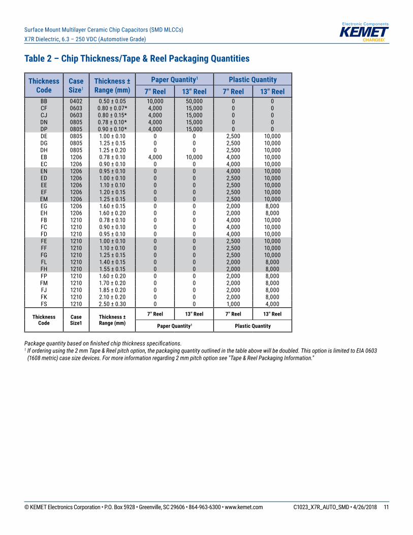
Table 2 – Chip Thickness/Tape & Reel Packaging Quantities
Package quantity based on finished chip thickness specifications.1 If ordering using the 2 mm Tape & Reel pitch option, the packaging quantity outlined in the table above will be doubled. This option is limited to EIA 0603
(1608 metric) case size devices. For more information regarding 2 mm pitch option see "Tape & Reel Packaging Information."
Thickness Code
Case Size1
Thickness ± Range (mm)
Paper Quantity1 Plastic Quantity7" Reel 13" Reel 7" Reel 13" Reel
BB 0402 0.50±0.05 10,000 50,000 0 0CF 0603 0.80±0.07* 4,000 15,000 0 0 CJ 0603 0.80±0.15* 4,000 15,000 0 0DN 0805 0.78±0.10* 4,000 15,000 0 0DP 0805 0.90±0.10* 4,000 15,000 0 0 DE 0805 1.00±0.10 0 0 2,500 10,000 DG 0805 1.25±0.15 0 0 2,500 10,000DH 0805 1.25±0.20 0 0 2,500 10,000 EB 1206 0.78±0.10 4,000 10,000 4,000 10,000EC 1206 0.90±0.10 0 0 4,000 10,000 EN 1206 0.95±0.10 0 0 4,000 10,000ED 1206 1.00±0.10 0 0 2,500 10,000 EE 1206 1.10±0.10 0 0 2,500 10,000EF 1206 1.20±0.15 0 0 2,500 10,000EM 1206 1.25±0.15 0 0 2,500 10,000EG 1206 1.60±0.15 0 0 2,000 8,000 EH 1206 1.60±0.20 0 0 2,000 8,000FB 1210 0.78±0.10 0 0 4,000 10,000 FC 1210 0.90±0.10 0 0 4,000 10,000FD 1210 0.95±0.10 0 0 4,000 10,000 FE 1210 1.00±0.10 0 0 2,500 10,000FF 1210 1.10±0.10 0 0 2,500 10,000FG 1210 1.25±0.15 0 0 2,500 10,000 FL 1210 1.40±0.15 0 0 2,000 8,000 FH 1210 1.55±0.15 0 0 2,000 8,000 FP 1210 1.60±0.20 0 0 2,000 8,000 FM 1210 1.70±0.20 0 0 2,000 8,000FJ 1210 1.85±0.20 0 0 2,000 8,000 FK 1210 2.10±0.20 0 0 2,000 8,000FS 1210 2.50±0.30 0 0 1,000 4,000
Thickness Code
Case Size1
Thickness ± Range (mm)
7" Reel 13" Reel 7" Reel 13" Reel
Paper Quantity1 Plastic Quantity
© KEMET Electronics Corporation • P.O. Box 5928 • Greenville, SC 29606 • 864-963-6300 • www.kemet.com C1023_X7R_AUTO_SMD • 4/26/2018 12
Surface Mount Multilayer Ceramic Chip Capacitors (SMD MLCCs) X7R Dielectric, 6.3 – 250 VDC (Automotive Grade)
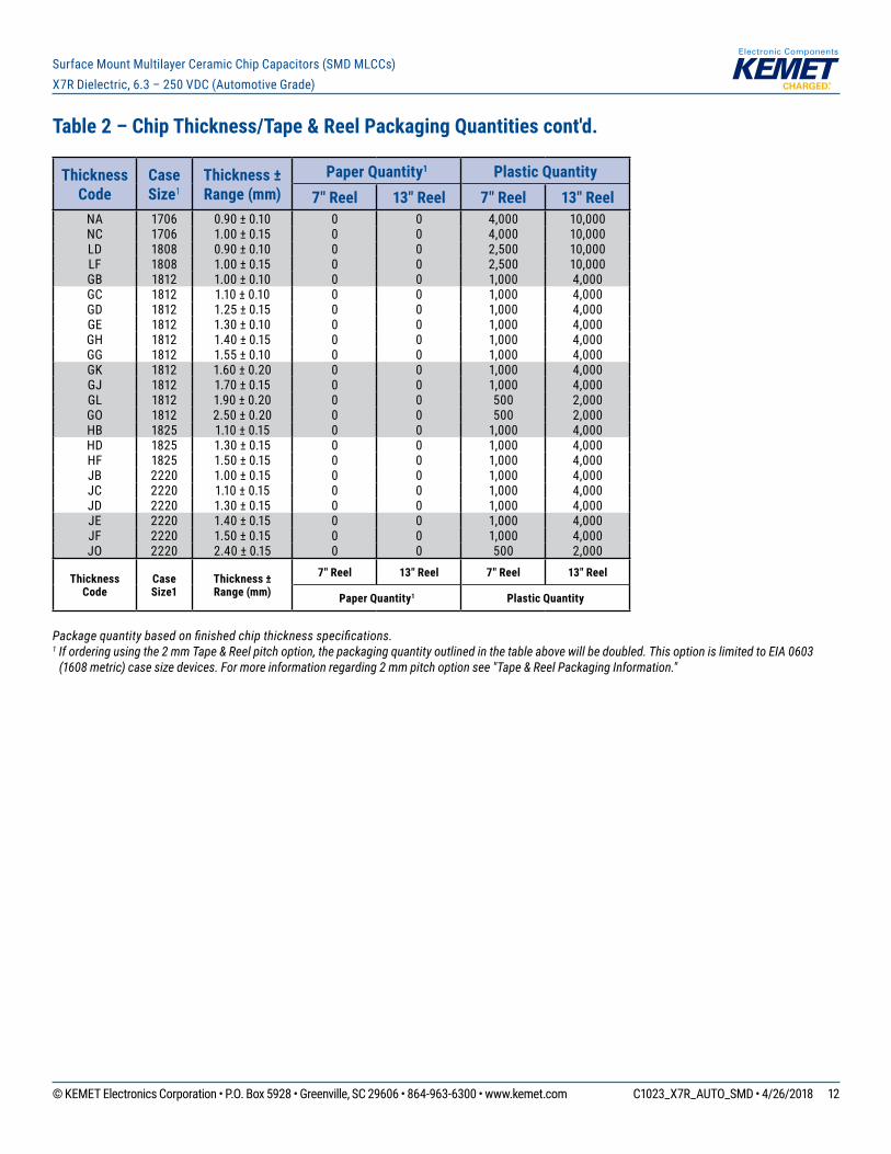
Table 2 – Chip Thickness/Tape & Reel Packaging Quantities cont'd.
Package quantity based on finished chip thickness specifications.1 If ordering using the 2 mm Tape & Reel pitch option, the packaging quantity outlined in the table above will be doubled. This option is limited to EIA 0603
(1608 metric) case size devices. For more information regarding 2 mm pitch option see "Tape & Reel Packaging Information."
Thickness Code
Case Size1
Thickness ± Range (mm)
Paper Quantity1 Plastic Quantity7" Reel 13" Reel 7" Reel 13" Reel
NA 1706 0.90±0.10 0 0 4,000 10,000 NC 1706 1.00±0.15 0 0 4,000 10,000 LD 1808 0.90±0.10 0 0 2,500 10,000 LF 1808 1.00±0.15 0 0 2,500 10,000 GB 1812 1.00±0.10 0 0 1,000 4,000GC 1812 1.10±0.10 0 0 1,000 4,000 GD 1812 1.25±0.15 0 0 1,000 4,000 GE 1812 1.30±0.10 0 0 1,000 4,000GH 1812 1.40±0.15 0 0 1,000 4,000 GG 1812 1.55±0.10 0 0 1,000 4,000GK 1812 1.60±0.20 0 0 1,000 4,000GJ 1812 1.70±0.15 0 0 1,000 4,000 GL 1812 1.90±0.20 0 0 500 2,000GO 1812 2.50±0.20 0 0 500 2,000HB 1825 1.10±0.15 0 0 1,000 4,000 HD 1825 1.30±0.15 0 0 1,000 4,000HF 1825 1.50±0.15 0 0 1,000 4,000JB 2220 1.00±0.15 0 0 1,000 4,000JC 2220 1.10±0.15 0 0 1,000 4,000JD 2220 1.30±0.15 0 0 1,000 4,000JE 2220 1.40±0.15 0 0 1,000 4,000JF 2220 1.50±0.15 0 0 1,000 4,000JO 2220 2.40±0.15 0 0 500 2,000
Thickness Code
Case Size1
Thickness ± Range (mm)
7" Reel 13" Reel 7" Reel 13" Reel
Paper Quantity1 Plastic Quantity
© KEMET Electronics Corporation • P.O. Box 5928 • Greenville, SC 29606 • 864-963-6300 • www.kemet.com C1023_X7R_AUTO_SMD • 4/26/2018 13
Surface Mount Multilayer Ceramic Chip Capacitors (SMD MLCCs) X7R Dielectric, 6.3 – 250 VDC (Automotive Grade)
Table 3 – Chip Capacitor Land Pattern Design Recommendations per IPC–7351
EIA Size Code
Metric Size Code
Density Level A: Maximum (Most)
Land Protrusion (mm)
Density Level B: Median (Nominal)
Land Protrusion (mm)
Density Level C: Minimum (Least)
Land Protrusion (mm)C Y X V1 V2 C Y X V1 V2 C Y X V1 V2
0402 1005 0.50 0.72 0.72 2.20 1.20 0.45 0.62 0.62 1.90 1.00 0.40 0.52 0.52 1.60 0.80
0603 1608 0.90 1.15 1.10 4.00 2.10 0.80 0.95 1.00 3.10 1.50 0.60 0.75 0.90 2.40 1.20
0805 2012 1.00 1.35 1.55 4.40 2.60 0.90 1.15 1.45 3.50 2.00 0.75 0.95 1.35 2.80 1.70
1206 3216 1.60 1.35 1.90 5.60 2.90 1.50 1.15 1.80 4.70 2.30 1.40 0.95 1.70 4.00 2.00
1210 3225 1.60 1.35 2.80 5.65 3.80 1.50 1.15 2.70 4.70 3.20 1.40 0.95 2.60 4.00 2.90
12101 3225 1.50 1.60 2.90 5.60 3.90 1.40 1.40 2.80 4.70 3.30 1.30 1.20 2.70 4.00 3.00
1812 4532 2.15 1.60 3.60 6.90 4.60 2.05 1.40 3.50 6.00 4.00 1.95 1.20 3.40 5.30 3.70
2220 5650 2.75 1.70 5.50 8.20 6.50 2.65 1.50 5.40 7.30 5.90 2.55 1.30 5.30 6.60 5.60
1 Only for capacitance values ≥ 22 µFDensity Level A: For low-density product applications. Recommended for wave solder applications and provides a wider process window for reflow solder processes. KEMET only recommends wave soldering of EIA 0603, 0805, and 1206 case sizes.Density Level B: For products with a moderate level of component density. Provides a robust solder attachment condition for reflow solder processes.Density Level C: For high component density product applications. Before adapting the minimum land pattern variations the user should perform qualification testing based on the conditions outlined in IPC Standard 7351 (IPC–7351).
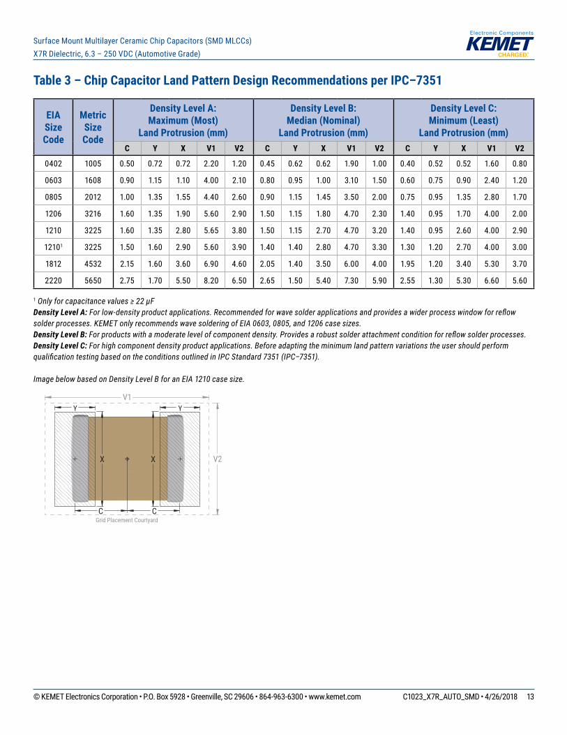
Image below based on Density Level B for an EIA 1210 case size.
Y
C C
X X
V1
V2
Grid Placement Courtyard
Y
© KEMET Electronics Corporation • P.O. Box 5928 • Greenville, SC 29606 • 864-963-6300 • www.kemet.com C1023_X7R_AUTO_SMD • 4/26/2018 14
Surface Mount Multilayer Ceramic Chip Capacitors (SMD MLCCs) X7R Dielectric, 6.3 – 250 VDC (Automotive Grade)
Soldering Process
Recommended Soldering Technique: •SolderwaveorsolderreflowforEIAcasesizes0603,0805and1206 •AllotherEIAcasesizesarelimitedtosolderreflowonly
Recommended Reflow Soldering Profile:TheKEMETfamiliesofsurfacemountmultilayerceramiccapacitors(SMDMLCCs)arecompatiblewithwave(singleordual),convection,IRorvaporphasereflowtechniques.Preheatingofthesecomponentsisrecommendedtoavoidextremethermalstress.TheKEMETrecommendedprofileconditionsforconvectionandIRreflowreflecttheprofileconditionsoftheIPC/J-STD-020standardformoisturesensitivitytesting.Thesedevicescansafelywithstandamaximumofthreereflowpassesattheseconditions.
Storage & Handling
Ceramicchipcapacitorsshouldbestoredinnormalworkingenvironments.Whilethechipsthemselvesarequiterobustinotherenvironments,solderabilitywillbedegradedbyexposuretohightemperatures,highhumidity,corrosiveatmospheres,andlongtermstorage.Inaddition,packagingmaterialswillbedegradedbyhightemperature–reelsmaysoftenorwarpandtapepeelforcemayincrease.KEMETrecommendsthatmaximumstoragetemperaturenotexceed40ºCandmaximumstoragehumiditynotexceed70%relativehumidity.Temperaturefluctuationsshouldbeminimizedtoavoidcondensationonthepartsandatmospheresshouldbefreeofchlorineandsulfurbearingcompounds.Foroptimizedsolderabilitychipstockshouldbeusedpromptly,preferablywithin1.5yearsofreceipt.
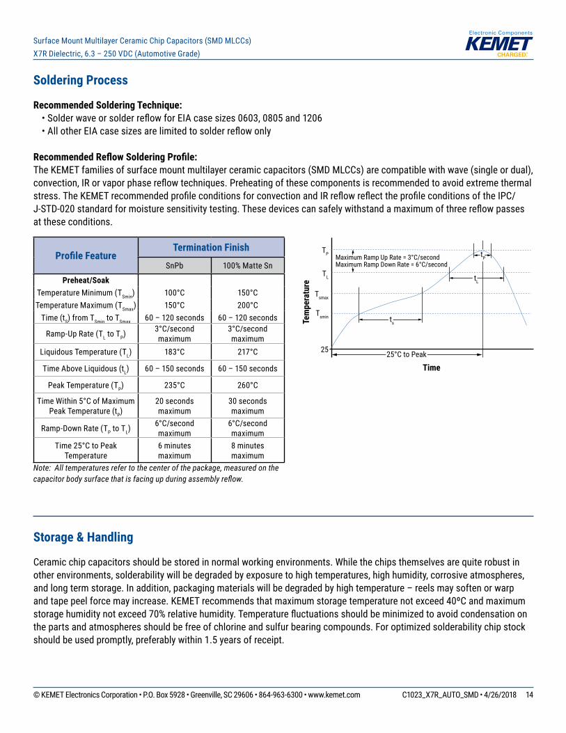
Profile FeatureTermination Finish
SnPb 100%MatteSn
Preheat/SoakTemperatureMinimum(TSmin) 100°C 150°CTemperatureMaximum(TSmax) 150°C 200°CTime(tS)fromTSmin to TSmax 60–120seconds 60–120seconds
Ramp-UpRate(TL to TP)3°C/secondmaximum
3°C/secondmaximum
LiquidousTemperature(TL) 183°C 217°C
TimeAboveLiquidous(tL) 60–150seconds 60–150seconds
PeakTemperature(TP) 235°C 260°C
TimeWithin5°CofMaximumPeakTemperature(tP)
20secondsmaximum
30secondsmaximum
Ramp-DownRate(TP to TL)6°C/secondmaximum
6°C/secondmaximum
Time25°CtoPeakTemperature
6 minutes maximum
8 minutes maximum
Note: All temperatures refer to the center of the package, measured on the capacitor body surface that is facing up during assembly reflow.
Time
Tem
pera
ture
Tsmin
25
Tsmax
TL
TP Maximum Ramp Up Rate = 3°C/secondMaximum Ramp Down Rate = 6°C/second
tP
tL
ts
25°C to Peak
© KEMET Electronics Corporation • P.O. Box 5928 • Greenville, SC 29606 • 864-963-6300 • www.kemet.com C1023_X7R_AUTO_SMD • 4/26/2018 15
Surface Mount Multilayer Ceramic Chip Capacitors (SMD MLCCs) X7R Dielectric, 6.3 – 250 VDC (Automotive Grade)
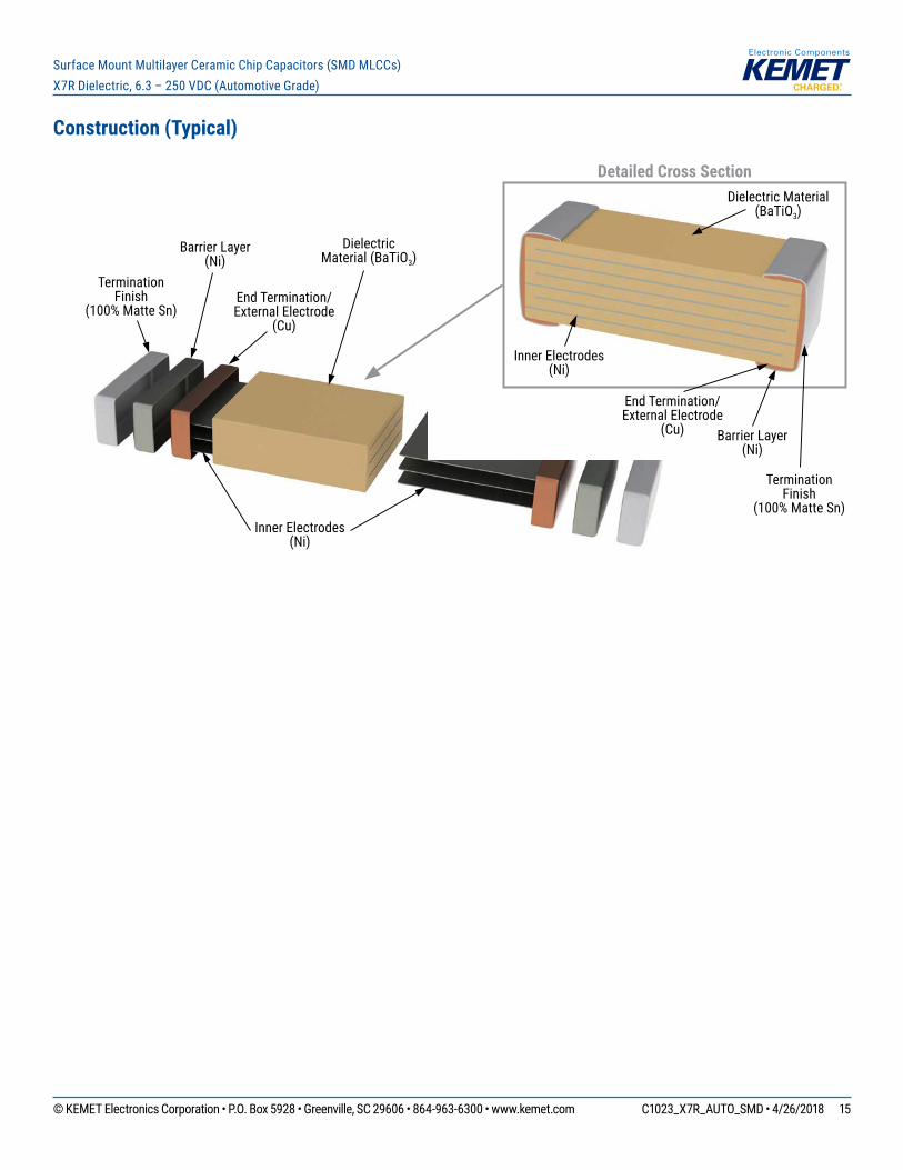
Construction (Typical)
Dielectric Material (BaTiO3)
Detailed Cross Section
Barrier Layer(Ni)
Inner Electrodes(Ni)
Barrier Layer(Ni)
Inner Electrodes(Ni)
Dielectric Material (BaTiO3)
Termination Finish
(100% Matte Sn)
Termination Finish
(100% Matte Sn)End Termination/External Electrode
(Cu)
End Termination/External Electrode
(Cu)
© KEMET Electronics Corporation • P.O. Box 5928 • Greenville, SC 29606 • 864-963-6300 • www.kemet.com C1023_X7R_AUTO_SMD • 4/26/2018 16
Surface Mount Multilayer Ceramic Chip Capacitors (SMD MLCCs) X7R Dielectric, 6.3 – 250 VDC (Automotive Grade)
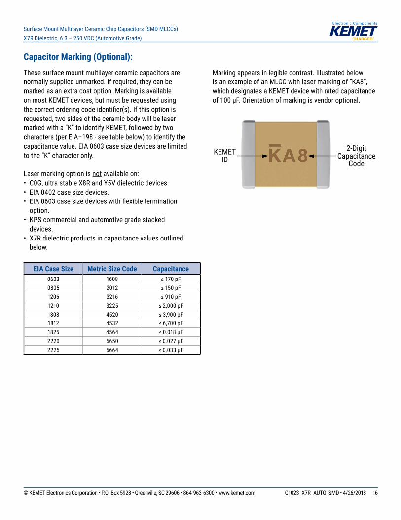
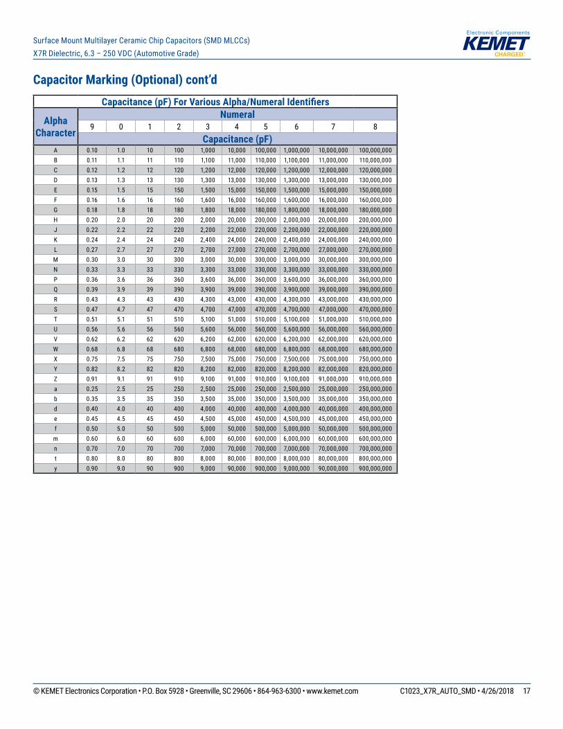
Capacitor Marking (Optional):Thesesurfacemountmultilayerceramiccapacitorsarenormallysuppliedunmarked.Ifrequired,theycanbemarkedasanextracostoption.MarkingisavailableonmostKEMETdevices,butmustberequestedusingthecorrectorderingcodeidentifier(s).Ifthisoptionisrequested,twosidesoftheceramicbodywillbelasermarkedwitha“K”toidentifyKEMET,followedbytwocharacters(perEIA–198-seetablebelow)toidentifythecapacitancevalue.EIA0603casesizedevicesarelimitedtothe“K”characteronly.
Lasermarkingoptionisnotavailableon:• C0G,ultrastableX8RandY5Vdielectricdevices.• EIA0402casesizedevices.• EIA0603casesizedeviceswithflexibletermination
option.• KPScommercialandautomotivegradestackeddevices.
• X7Rdielectricproductsincapacitancevaluesoutlinedbelow.
Markingappearsinlegiblecontrast.IllustratedbelowisanexampleofanMLCCwithlasermarkingof“KA8”,whichdesignatesaKEMETdevicewithratedcapacitanceof100µF.Orientationofmarkingisvendoroptional.
KEMET ID
2-Digit Capacitance
Code
EIA Case Size Metric Size Code Capacitance0603 1608 ≤170pF0805 2012 ≤150pF1206 3216 ≤910pF1210 3225 ≤2,000pF1808 4520 ≤3,900pF1812 4532 ≤6,700pF1825 4564 ≤0.018µF2220 5650 ≤0.027µF2225 5664 ≤0.033µF
© KEMET Electronics Corporation • P.O. Box 5928 • Greenville, SC 29606 • 864-963-6300 • www.kemet.com C1023_X7R_AUTO_SMD • 4/26/2018 17
Surface Mount Multilayer Ceramic Chip Capacitors (SMD MLCCs) X7R Dielectric, 6.3 – 250 VDC (Automotive Grade)
Capacitor Marking (Optional) cont’dCapacitance (pF) For Various Alpha/Numeral Identifi ers
AlphaCharacter
Numeral9 0 1 2 3 4 5 6 7 8
Capacitance (pF)A 0.10 1.0 10 100 1,000 10,000 100,000 1,000,000 10,000,000 100,000,000B 0.11 1.1 11 110 1,100 11,000 110,000 1,100,000 11,000,000 110,000,000C 0.12 1.2 12 120 1,200 12,000 120,000 1,200,000 12,000,000 120,000,000D 0.13 1.3 13 130 1,300 13,000 130,000 1,300,000 13,000,000 130,000,000E 0.15 1.5 15 150 1,500 15,000 150,000 1,500,000 15,000,000 150,000,000F 0.16 1.6 16 160 1,600 16,000 160,000 1,600,000 16,000,000 160,000,000G 0.18 1.8 18 180 1,800 18,000 180,000 1,800,000 18,000,000 180,000,000H 0.20 2.0 20 200 2,000 20,000 200,000 2,000,000 20,000,000 200,000,000J 0.22 2.2 22 220 2,200 22,000 220,000 2,200,000 22,000,000 220,000,000K 0.24 2.4 24 240 2,400 24,000 240,000 2,400,000 24,000,000 240,000,000L 0.27 2.7 27 270 2,700 27,000 270,000 2,700,000 27,000,000 270,000,000M 0.30 3.0 30 300 3,000 30,000 300,000 3,000,000 30,000,000 300,000,000N 0.33 3.3 33 330 3,300 33,000 330,000 3,300,000 33,000,000 330,000,000P 0.36 3.6 36 360 3,600 36,000 360,000 3,600,000 36,000,000 360,000,000Q 0.39 3.9 39 390 3,900 39,000 390,000 3,900,000 39,000,000 390,000,000R 0.43 4.3 43 430 4,300 43,000 430,000 4,300,000 43,000,000 430,000,000S 0.47 4.7 47 470 4,700 47,000 470,000 4,700,000 47,000,000 470,000,000T 0.51 5.1 51 510 5,100 51,000 510,000 5,100,000 51,000,000 510,000,000U 0.56 5.6 56 560 5,600 56,000 560,000 5,600,000 56,000,000 560,000,000V 0.62 6.2 62 620 6,200 62,000 620,000 6,200,000 62,000,000 620,000,000W 0.68 6.8 68 680 6,800 68,000 680,000 6,800,000 68,000,000 680,000,000X 0.75 7.5 75 750 7,500 75,000 750,000 7,500,000 75,000,000 750,000,000Y 0.82 8.2 82 820 8,200 82,000 820,000 8,200,000 82,000,000 820,000,000Z 0.91 9.1 91 910 9,100 91,000 910,000 9,100,000 91,000,000 910,000,000a 0.25 2.5 25 250 2,500 25,000 250,000 2,500,000 25,000,000 250,000,000b 0.35 3.5 35 350 3,500 35,000 350,000 3,500,000 35,000,000 350,000,000d 0.40 4.0 40 400 4,000 40,000 400,000 4,000,000 40,000,000 400,000,000e 0.45 4.5 45 450 4,500 45,000 450,000 4,500,000 45,000,000 450,000,000f 0.50 5.0 50 500 5,000 50,000 500,000 5,000,000 50,000,000 500,000,000m 0.60 6.0 60 600 6,000 60,000 600,000 6,000,000 60,000,000 600,000,000n 0.70 7.0 70 700 7,000 70,000 700,000 7,000,000 70,000,000 700,000,000t 0.80 8.0 80 800 8,000 80,000 800,000 8,000,000 80,000,000 800,000,000y 0.90 9.0 90 900 9,000 90,000 900,000 9,000,000 90,000,000 900,000,000
© KEMET Electronics Corporation • P.O. Box 5928 • Greenville, SC 29606 • 864-963-6300 • www.kemet.com C1023_X7R_AUTO_SMD • 4/26/2018 18
Surface Mount Multilayer Ceramic Chip Capacitors (SMD MLCCs) X7R Dielectric, 6.3 – 250 VDC (Automotive Grade)
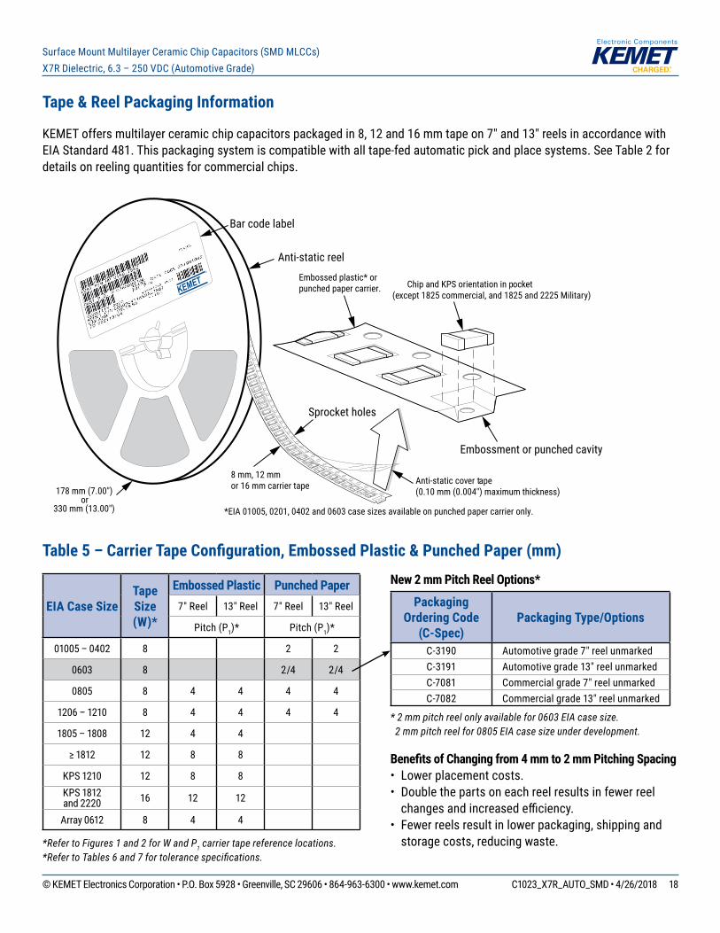
Tape & Reel Packaging Information
KEMEToffersmultilayerceramicchipcapacitorspackagedin8,12and16mmtapeon7"and13"reelsinaccordancewithEIAStandard481.Thispackagingsystemiscompatiblewithalltape-fedautomaticpickandplacesystems.SeeTable2fordetailsonreelingquantitiesforcommercialchips.
8 mm, 12 mmor 16 mm carrier tape 178 mm (7.00")
or330 mm (13.00")
Anti-static reel
Embossed plastic* or punched paper carrier.
Embossment or punched cavity
Anti-static cover tape(0.10 mm (0.004") maximum thickness)
Chip and KPS orientation in pocket(except 1825 commercial, and 1825 and 2225 Military)
*EIA 01005, 0201, 0402 and 0603 case sizes available on punched paper carrier only.
KEMET®
Bar code label
Sprocket holes
Table 5 – Carrier Tape Confi guration, Embossed Plastic & Punched Paper (mm)
EIA Case SizeTape Size (W)*
Embossed Plastic Punched Paper7"Reel 13"Reel 7"Reel 13"Reel
Pitch(P1)* Pitch(P1)*
01005 – 0402 8 2 2
0603 8 2/4 2/4
0805 8 4 4 4 4
1206 – 1210 8 4 4 4 4
1805 – 1808 12 4 4
≥1812 12 8 8
KPS 1210 12 8 8KPS 1812and2220 16 12 12
Array0612 8 4 4
*Refer to Figures 1 and 2 for W and P1 carrier tape reference locations.*Refer to Tables 6 and 7 for tolerance specifi cations.
New 2 mm Pitch Reel Options*
PackagingOrdering Code
(C-Spec)Packaging Type/Options
C-3190 Automotivegrade7"reelunmarkedC-3191 Automotivegrade13"reelunmarkedC-7081 Commercialgrade7"reelunmarkedC-7082 Commercialgrade13"reelunmarked
* 2 mm pitch reel only available for 0603 EIA case size. 2 mm pitch reel for 0805 EIA case size under development.
Benefi ts of Changing from 4 mm to 2 mm Pitching Spacing• Lower placement costs.• Doublethepartsoneachreelresultsinfewerreelchangesandincreasedefficiency.
• Fewerreelsresultinlowerpackaging,shippingandstoragecosts,reducingwaste.
© KEMET Electronics Corporation • P.O. Box 5928 • Greenville, SC 29606 • 864-963-6300 • www.kemet.com C1023_X7R_AUTO_SMD • 4/26/2018 19
Surface Mount Multilayer Ceramic Chip Capacitors (SMD MLCCs) X7R Dielectric, 6.3 – 250 VDC (Automotive Grade)
Figure 1 – Embossed (Plastic) Carrier Tape Dimensions
P0
T
F
W
Center Lines of Cavity
A0
B0
User Direction of Unreeling
Cover Tape
K0
B1 is for tape feeder reference only, including draft concentric about B0.
T2
ØD1
ØD0
B1
S1
T1
E1
E2
P1
P2
EmbossmentFor cavity size,see Note 1 Table 4
(10 pitches cumulativetolerance on tape ±0.2 mm)
Table 6 – Embossed (Plastic) Carrier Tape DimensionsMetricwillgovern
Constant Dimensions — Millimeters (Inches)
Tape Size D0 D1 Minimum
Note 1 E1 P0 P2 RReference
Note 2S1 Minimum
Note 3T
MaximumT1
Maximum
8 mm
1.5+0.10/−0.0(0.059+0.004/−0.0)
1.0 (0.039)
1.75±0.10(0.069±0.004)
4.0±0.10(0.157±0.004)
2.0±0.05(0.079±0.002)
25.0 (0.984)
0.600 (0.024)
0.600 (0.024)
0.100 (0.004)12 mm
1.5 (0.059)
30 (1.181)
16 mm
Variable Dimensions — Millimeters (Inches)
Tape Size Pitch B1 MaximumNote 4
E2 Minimum F P1
T2 Maximum
W Maximum A0,B0 & K0
8 mm Single(4mm) 4.35 (0.171)
6.25 (0.246)
3.5±0.05(0.138±0.002)
4.0±0.10(0.157±0.004)
2.5 (0.098)
8.3 (0.327)
Note 512 mm Single(4mm)anddouble(8mm)
8.2 (0.323)
10.25 (0.404)
5.5±0.05(0.217±0.002)
8.0±0.10(0.315±0.004)
4.6 (0.181)
12.3 (0.484)
16 mm Triple(12mm) 12.1 (0.476)
14.25(0.561)
7.5±0.05(0.138±0.002)
12.0±0.10(0.157±0.004)
4.6 (0.181)
16.3 (0.642)
1. The embossment hole location shall be measured from the sprocket hole controlling the location of the embossment. Dimensions of the embossment location and the hole location shall be applied independently of each other.
2. The tape with or without components shall pass around R without damage (see Figure 6.)3. If S1 < 1.0 mm, there may not be enough area for a cover tape to be properly applied (see EIA Standard 481, paragraph 4.3, section b.)4. B1 dimension is a reference dimension for tape feeder clearance only.5. The cavity defi ned by A0, B0 and K0 shall surround the component with suffi cient clearance that: (a) the component does not protrude above the top surface of the carrier tape. (b) the component can be removed from the cavity in a vertical direction without mechanical restriction, after the top cover tape has been
removed. (c) rotation of the component is limited to 20° maximum for 8 and 12 mm tapes and 10° maximum for 16 mm tapes (see Figure 3.) (d) lateral movement of the component is restricted to 0.5 mm maximum for 8 and 12 mm wide tape and to 1.0 mm maximum for 16 mm tape
(see Figure 4.) (e) for KPS product, A0 and B0 are measured on a plane 0.3 mm above the bottom of the pocket. (f) see addendum in EIA Standard 481 for standards relating to more precise taping requirements.
© KEMET Electronics Corporation • P.O. Box 5928 • Greenville, SC 29606 • 864-963-6300 • www.kemet.com C1023_X7R_AUTO_SMD • 4/26/2018 20
Surface Mount Multilayer Ceramic Chip Capacitors (SMD MLCCs) X7R Dielectric, 6.3 – 250 VDC (Automotive Grade)
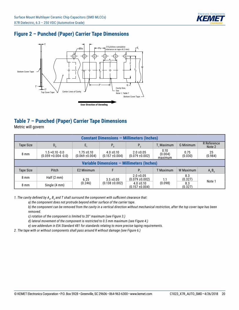
Figure 2 – Punched (Paper) Carrier Tape Dimensions
User Direction of Unreeling
Top Cover Tape
T
Center Lines of Cavity
P1
ØDo Po E1
F
E2
W
G
A0
B0
Cavity Size,SeeNote 1, Table 7
Bottom Cover Tape
T1
T1
Bottom Cover Tape
(10 pitches cumulativetolerance on tape ±0.2 mm)
Table 7 – Punched (Paper) Carrier Tape Dimensions Metricwillgovern
Constant Dimensions — Millimeters (Inches)Tape Size D0 E1 P0 P2 T1 Maximum G Minimum RReference
Note 2
8 mm 1.5+0.10-0.0(0.059+0.004-0.0)
1.75±0.10(0.069±0.004)
4.0±0.10(0.157±0.004)
2.0±0.05(0.079±0.002)
0.10 (0.004)
maximum0.75
(0.030)25
(0.984)
Variable Dimensions — Millimeters (Inches)Tape Size Pitch E2 Minimum F P1 T Maximum W Maximum A0 B0
8 mm Half(2mm) 6.25 (0.246)
3.5±0.05(0.138±0.002)
2.0±0.05(0.079±0.002) 1.1
(0.098)
8.3(0.327) Note 1
8 mm Single(4mm) 4.0±0.10(0.157±0.004)
8.3(0.327)
1. The cavity defi ned by A0, B0 and T shall surround the component with suffi cient clearance that: a) the component does not protrude beyond either surface of the carrier tape. b) the component can be removed from the cavity in a vertical direction without mechanical restriction, after the top cover tape has been
removed. c) rotation of the component is limited to 20° maximum (see Figure 3.) d) lateral movement of the component is restricted to 0.5 mm maximum (see Figure 4.) e) see addendum in EIA Standard 481 for standards relating to more precise taping requirements.2. The tape with or without components shall pass around R without damage (see Figure 6.)
© KEMET Electronics Corporation • P.O. Box 5928 • Greenville, SC 29606 • 864-963-6300 • www.kemet.com C1023_X7R_AUTO_SMD • 4/26/2018 21
Surface Mount Multilayer Ceramic Chip Capacitors (SMD MLCCs) X7R Dielectric, 6.3 – 250 VDC (Automotive Grade)
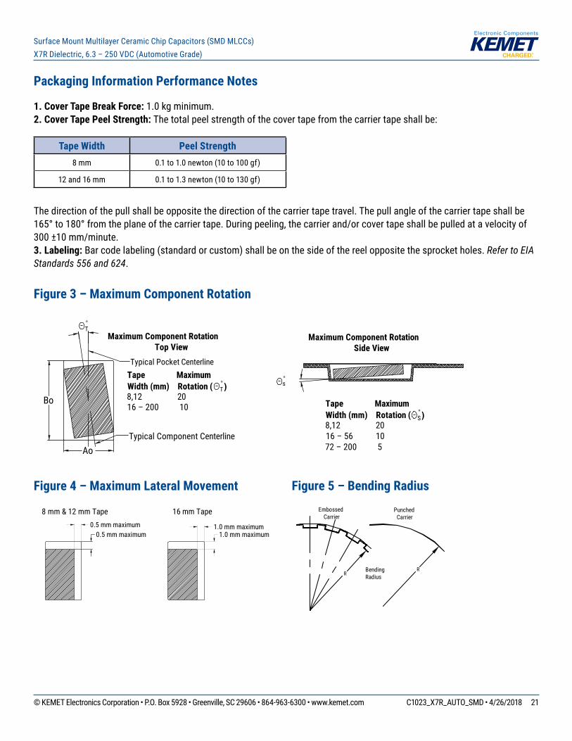
Packaging Information Performance Notes
1. Cover Tape Break Force:1.0kgminimum.2. Cover Tape Peel Strength: Thetotalpeelstrengthofthecovertapefromthecarriertapeshallbe:
Tape Width Peel Strength8 mm 0.1to1.0newton(10to100gf)
12and16mm 0.1to1.3newton(10to130gf)
Thedirectionofthepullshallbeoppositethedirectionofthecarriertapetravel.Thepullangleofthecarriertapeshallbe165°to180°fromtheplaneofthecarriertape.Duringpeeling,thecarrierand/orcovertapeshallbepulledatavelocityof300±10mm/minute.3. Labeling:Barcodelabeling(standardorcustom)shallbeonthesideofthereeloppositethesprocketholes.Refer to EIA Standards 556 and 624.
Figure 3 – Maximum Component Rotation
Ao
Bo
°T
°s
Maximum Component RotationTop View
Maximum Component RotationSide View
Tape MaximumWidth (mm) Rotation ( °
T)8,12 20 16 – 200 10 Tape Maximum
Width (mm) Rotation ( °S)
8,12 20 16 – 56 1072 – 200 5
Typical Pocket Centerline
Typical Component Centerline
Figure 4 – Maximum Lateral Movement
0.5 mm maximum0.5 mm maximum
8 mm & 12 mm Tape
1.0 mm maximum1.0 mm maximum
16 mm Tape
Figure 5 – Bending Radius
RRBending
Radius
EmbossedCarrier
PunchedCarrier
© KEMET Electronics Corporation • P.O. Box 5928 • Greenville, SC 29606 • 864-963-6300 • www.kemet.com C1023_X7R_AUTO_SMD • 4/26/2018 22
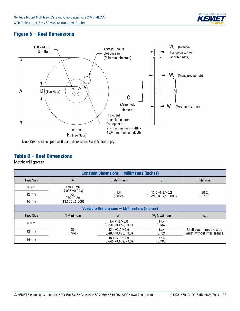
Surface Mount Multilayer Ceramic Chip Capacitors (SMD MLCCs) X7R Dielectric, 6.3 – 250 VDC (Automotive Grade)
Figure 6 – Reel Dimensions
A D (See Note)
Full Radius,See Note
B (see Note)
Access Hole atSlot Location(Ø 40 mm minimum)
If present,tape slot in corefor tape start:2.5 mm minimum width x10.0 mm minimum depth
W3 (Includes flange distortion at outer edge)
W2 (Measured at hub)
W1 (Measured at hub)
C(Arbor holediameter)
Note: Drive spokes optional; if used, dimensions B and D shall apply.
N
Table 8 – Reel DimensionsMetricwillgovern
Constant Dimensions — Millimeters (Inches) Tape Size A B Minimum C D Minimum
8 mm 178±0.20(7.008±0.008)
or330±0.20
(13.000±0.008)
1.5 (0.059)
13.0+0.5/−0.2(0.521+0.02/−0.008)
20.2 (0.795)12 mm
16 mm
Variable Dimensions — Millimeters (Inches) Tape Size N Minimum W1 W2 Maximum W3
8 mm
50 (1.969)
8.4+1.5/−0.0(0.331+0.059/−0.0)
14.4 (0.567)
Shallaccommodatetapewidthwithoutinterference12 mm 12.4+2.0/−0.0
(0.488+0.078/−0.0)18.4
(0.724)
16 mm 16.4+2.0/−0.0(0.646+0.078/−0.0)
22.4 (0.882)
© KEMET Electronics Corporation • P.O. Box 5928 • Greenville, SC 29606 • 864-963-6300 • www.kemet.com C1023_X7R_AUTO_SMD • 4/26/2018 23
Surface Mount Multilayer Ceramic Chip Capacitors (SMD MLCCs) X7R Dielectric, 6.3 – 250 VDC (Automotive Grade)
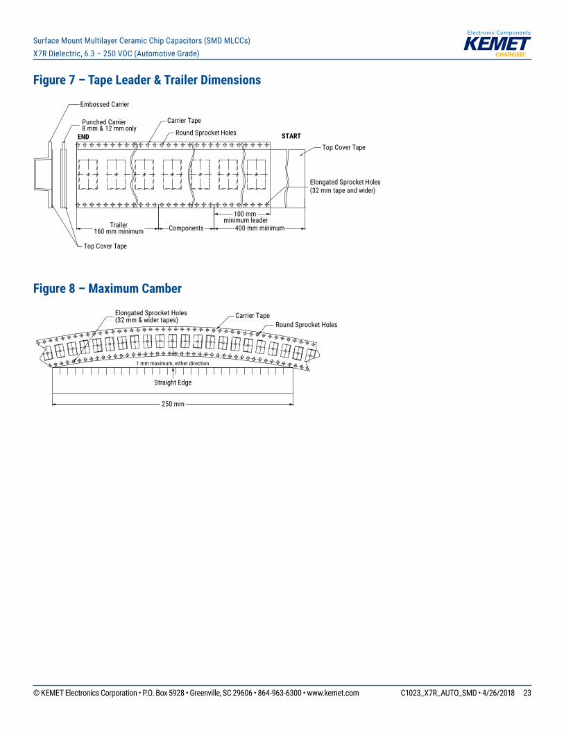
Figure 7 – Tape Leader & Trailer Dimensions
Trailer160 mm minimum
Carrier Tape
END STARTRound Sprocket Holes
Elongated Sprocket Holes(32 mm tape and wider)
Top Cover Tape
Top Cover Tape
Punched Carrier8 mm & 12 mm only
Embossed Carrier
Components
100 mm minimum leader
400 mm minimum
Figure 8 – Maximum Camber
Carrier TapeRound Sprocket Holes
1 mm maximum, either direction
Straight Edge
250 mm
Elongated Sprocket Holes(32 mm & wider tapes)
© KEMET Electronics Corporation • P.O. Box 5928 • Greenville, SC 29606 • 864-963-6300 • www.kemet.com C1023_X7R_AUTO_SMD • 4/26/2018 24
Surface Mount Multilayer Ceramic Chip Capacitors (SMD MLCCs) X7R Dielectric, 6.3 – 250 VDC (Automotive Grade)
KEMET Electronics Corporation Sales Offi ces
Foracompletelistofourglobalsalesoffices,pleasevisitwww.kemet.com/sales.
DisclaimerAllproductspecifications,statements,informationanddata(collectively,the“Information”)inthisdatasheetaresubjecttochange.ThecustomerisresponsibleforcheckingandverifyingtheextenttowhichtheInformationcontainedinthispublicationisapplicabletoanorderatthetimetheorderisplaced.
AllInformationgivenhereinisbelievedtobeaccurateandreliable,butitispresentedwithoutguarantee,warranty,orresponsibilityofanykind,expressedorimplied.
StatementsofsuitabilityforcertainapplicationsarebasedonKEMETElectronicsCorporation’s(“KEMET”)knowledgeoftypicaloperatingconditionsforsuchapplications,butarenotintendedtoconstitute–andKEMETspecificallydisclaims–anywarrantyconcerningsuitabilityforaspecificcustomerapplicationoruse.TheInformationisintendedforuseonlybycustomerswhohavetherequisiteexperienceandcapabilitytodeterminethecorrectproductsfortheirapplication.AnytechnicaladviceinferredfromthisInformationorotherwiseprovidedbyKEMETwithreferencetotheuseofKEMET’sproductsisgivengratis,andKEMETassumesnoobligationorliabilityfortheadvicegivenorresultsobtained.
AlthoughKEMETdesignsandmanufacturesitsproductstothemoststringentqualityandsafetystandards,giventhecurrentstateoftheart,isolatedcomponentfailuresmaystilloccur.Accordingly,customerapplicationswhichrequireahighdegreeofreliabilityorsafetyshouldemploysuitabledesignsorothersafeguards(suchasinstallationofprotectivecircuitryorredundancies)inordertoensurethatthefailureofanelectricalcomponentdoesnotresultinariskofpersonalinjuryorpropertydamage.
Althoughallproduct–relatedwarnings,cautionsandnotesmustbeobserved,thecustomershouldnotassumethatallsafetymeasuresareindictedorthatothermeasuresmaynotberequired.
KEMET is a registered trademark of KEMET Electronics Corporation.