Embed Size (px)
Citation preview
1© KEMET Electronics Corporation • KEMET Tower • One East Broward Boulevard C1018_X7R_SnPb_SMD • 11/8/2018Fort Lauderdale, FL 33301 USA • 954-766-2800 • www.kemet.com
One world. One KEMET
Benefits
• −55°Cto+125°Coperatingtemperaturerange• Temperature stable dielectric• Reliable and robust termination system• EIA 0402, 0603, 0805, 1206, 1210, 1808, 1812, 1825, 2220
and 2225 case sizes• DCvoltageratingsof6.3V,10V,16V,25V,50V,100V,200Vand250V
• Capacitanceofferingsrangingfrom10pFto22μF• Availablecapacitancetolerancesof±5%,±10%and±20%• Non-polardevice,minimizinginstallationconcerns• SnPbplatedterminationfinish(5%Pbminimum)• Flexible termination option available upon request•Availableforothersurfacemountproducts,additionaldielectricsandhighervoltageratingsuponrequest
Overview
TheKEMETCommercial"L"surfacemountcapacitorswithtinandleadterminationinX7Rdielectricaredesignedtomeettheneedsofcriticalapplications,wheretinandlead end metallization is required. KEMET’s tin and lead electroplatingprocessisdesignedtomeeta5%minimumleadcontent,aswellasaddressconcernsforamorerobustandreliableleadcontainingterminationsystem.AsthebulkoftheelectronicsindustrymovestowardsRoHS compliance, KEMET continues to provide tin and leadterminatedproductsforthemilitary,aerospaceandindustrialapplications,andwillensurecustomershaveastableandlong-termsourceofsupply.
TheKEMETX7Rdielectricfeaturesa125°Cmaximumoperatingtemperatureandisconsideredtemperaturestable.TheElectronicsIndustriesAlliance(EIA)characterizesX7RdielectricasaClassIImaterial.Componentsofthisclassificationarefixed,ceramicdielectriccapacitorssuitedforbypassanddecouplingapplicationsorforfrequencydiscriminatingcircuits,whereQandstabilityofcapacitancecharacteristicsarenotcritical.X7Rexhibitsapredictablechangeincapacitancewithrespecttotimeandvoltage,boastingaminimalchangeincapacitancewithreferencetoambienttemperature.Capacitancechangeislimitedto±15%from–55°Cto+125°C.
SurfaceMountMultilayerCeramicChipCapacitors(SMDMLCCs)
Commercial "L", SnPb Termination, X7R Dielectric6.3 – 250 VDC (Commercial Grade)
Applications
Typicalapplicationsincludemilitary,aerospaceandotherhighreliabilityapplications.
2© KEMET Electronics Corporation • KEMET Tower • One East Broward Boulevard C1018_X7R_SnPb_SMD • 11/8/2018Fort Lauderdale, FL 33301 USA • 954-766-2800 • www.kemet.com
Surface Mount Multilayer Ceramic Chip Capacitors (SMD MLCCs)Commercial "L", SnPb Termination, X7R Dielectric, 6.3 – 250 VDC (Commercial Grade)
Ordering Information
C 1210 C 226 K 8 R A L TU
CeramicCase Size (L"xW")
Specification/Series
Capacitance Code(pF)
Capacitance Tolerance
Rated Voltage(VDC)
DielectricFailure Rate/Design
TerminationFinish1 Packaging/Grade(C-Spec)
0402060308051206121018081812182522202225
C = Standard Two SignificantDigitsandNumberof
Zeros
J=±5%K=±10%M=±20%
9 = 6.38 = 104 = 163 = 256 = 355 = 501 = 1002 = 200A = 250
R = X7R A = N/A L=SnPb(5%Pbminimum) See“PackagingC-SpecOrderingOptions Table”
1 Additional termination finish options may be available. Contact KEMET for details.
Packaging C-Spec Ordering Options Table
Packaging Type1 Packaging/Grade Ordering Code (C-Spec)
BulkBag/Unmarked Notrequired(Blank)7"Reel/Unmarked TU
13"Reel/Unmarked 7411(EIA0603andsmallercasesizes)7210(EIA0805andlargercasesizes)
7"Reel/Marked TM
13"Reel/Marked 7040(EIA0603)7215(EIA0805andlargercasesizes)
7"Reel/Unmarked/2mmpitch2 708113"Reel/Unmarked/2mmpitch2 7082
1 Default packaging is "Bulk Bag." An ordering code C-Spec is not required for "Bulk Bag" packaging.1 The terms "Marked" and "Unmarked" pertain to laser marking option of capacitors. All packaging options labeled as "Unmarked" will contain capacitors
that have not been laser marked. Please contact KEMET if you require a laser marked option. For more information see "Capacitor Marking."2 The 2 mm pitch option allows for double the packaging quantity of capacitors on a given reel size. This option is limited to EIA 0603 (1608 metric) case
size devices. For more information regarding 2 mm pitch option see "Tape & Reel Packaging Information."
3© KEMET Electronics Corporation • KEMET Tower • One East Broward Boulevard C1018_X7R_SnPb_SMD • 11/8/2018Fort Lauderdale, FL 33301 USA • 954-766-2800 • www.kemet.com
Surface Mount Multilayer Ceramic Chip Capacitors (SMD MLCCs)Commercial "L", SnPb Termination, X7R Dielectric, 6.3 – 250 VDC (Commercial Grade)
Dimensions – Millimeters (Inches)
L
B
W
S
T
EIA Size Code
Metric Size Code
L Length
W Width T Thickness B
Bandwidth
SSeparation Minimum
Mounting Technique
0402 1005 1.00(0.040) ±0.05(0.002)
0.50(0.020) ±0.05(0.002)
SeeTable2forThickness
0.30(0.012) ±0.10(0.004) 0.30(0.012) Solderreflowonly
0603 1608 1.60(0.063) ±0.15(0.006)
0.80(0.032) ±0.15(0.006)
0.35(0.014) ±0.15(0.006) 0.70(0.028)
Solder wave or Solderreflow0805 2012 2.00(0.079)
±0.20(0.008)1.25(0.049) ±0.20(0.008)
0.50(0.02) ±0.25(0.010) 0.75(0.030)
1206 3216 3.20(0.126) ±0.20(0.008)
1.60(0.063) ±0.20(0.008)
0.50(0.02) ±0.25(0.010)
N/A
1210 3225 3.20(0.126) ±0.20(0.008)
2.50(0.098) ±0.20(0.008)
0.50(0.02) ±0.25(0.010)
Solderreflowonly
1808 4520 4.70(0.185) ±0.50(0.020)
2.00(0.079) ±0.20(0.008)
0.60(0.024) ±0.35(0.014)
1812 4532 4.50(0.177) ±0.30(0.012)
3.20(0.126) ±0.30(0.012)
0.60(0.024) ±0.35(0.014)
1825 4564 4.50(0.177) ±0.30(0.012)
6.40(0.252) ±0.40(0.016)
0.60(0.024) ±0.35(0.014)
2220 5650 5.70(0.224) ±0.40(0.016)
5.00(0.197) ±0.40(0.016)
0.60(0.024) ±0.35(0.014)
2225 5664 5.60(0.220) ±0.40(0.016)
6.40(0.248) ±0.40(0.016)
0.60(0.024) ±0.35(0.014)
4© KEMET Electronics Corporation • KEMET Tower • One East Broward Boulevard C1018_X7R_SnPb_SMD • 11/8/2018Fort Lauderdale, FL 33301 USA • 954-766-2800 • www.kemet.com
Surface Mount Multilayer Ceramic Chip Capacitors (SMD MLCCs)Commercial "L", SnPb Termination, X7R Dielectric, 6.3 – 250 VDC (Commercial Grade)
Qualification/Certification
Commercialgradeproductsaresubjecttointernalqualification.DetailsregardingtestmethodsandconditionsarereferencedinTable4,Performance&Reliability.
Environmental Compliance
ThesedevicesdonotmeetRoHScriteriaduetotheconcentrationofLead(Pb)intheterminationfinish.
Electrical Parameters/Characteristics
Item Parameters/CharacteristicsOperatingTemperatureRange −55°Cto+125°C
CapacitanceChangewithReferenceto +25°Cand0VdcApplied(TCC) ±15%
1AgingRate(Maximum%CapacitanceLoss/DecadeHour) 3.0%
2DielectricWithstandingVoltage(DWV) 250%ofratedvoltage (5±1secondsandcharge/dischargenotexceeding50mA)
3DissipationFactor(DF)MaximumLimitat25°C 5%(6.3Vand10V),3.5%(16Vand25V)and2.5%(50Vto250V)
4InsulationResistance(IR)MinimumLimitat25°C See Insulation Resistance Limit Table (Ratedvoltageappliedfor120±5secondsat25°C)
1 Regarding Aging Rate: Capacitance measurements (including tolerance) are indexed to a referee time of 1,000 hours.2 DWV is the voltage a capacitor can withstand (survive) for a short period of time. It exceeds the nominal and continuous working voltage of the
capacitor.3 Capacitance and dissipation factor (DF) measured under the following conditions: 1 kHz ±50 Hz and 1.0 ±0.2 Vrms if capacitance ≤ 10 µF 120 Hz ±10 Hz and 0.5 ±0.1 Vrms if capacitance > 10 µF4 To obtain IR limit, divide MΩ-µF value by the capacitance and compare to GΩ limit. Select the lower of the two limits.Note: When measuring capacitance it is important to ensure the set voltage level is held constant. The HP4284 and Agilent E4980 have a feature known as Automatic Level Control (ALC). The ALC feature should be switched to "ON."
5© KEMET Electronics Corporation • KEMET Tower • One East Broward Boulevard C1018_X7R_SnPb_SMD • 11/8/2018Fort Lauderdale, FL 33301 USA • 954-766-2800 • www.kemet.com
Surface Mount Multilayer Ceramic Chip Capacitors (SMD MLCCs)Commercial "L", SnPb Termination, X7R Dielectric, 6.3 – 250 VDC (Commercial Grade)
Post Environmental Limits
High Temperature Life, Biased Humidity, Moisture Resistance
Dielectric Rated DCVoltage
CapacitanceValue
Dissipation Factor (Maximum%)
CapacitanceShift
Insulation Resistance
X7R> 25
All3.0
±20% 10%ofInitiallimit16/25 5.0
< 16 7.5
Insulation Resistance Limit Table
EIA Case Size Rated DC Voltage 1,000 megohm microfarads or 100 GΩ
500 megohm microfarads or 10 GΩ
100 megohm microfarads or 10 GΩ
0201 ALL N/A ALL N/A0402 ALL < .012 µF ≥.012µF N/A
0603≤200V < .047 µF ≥.047µF N/A250V N/A N/A ALL
0805≤200V < 0.15 µF ≥0.15µF N/A250V < .027 µF N/A ≥.027µF
1206≤200V < 0.47 µF ≥0.47µF N/A250V < 0.12 µF N/A ≥0.12µF
1210≤200V < 0.39 µF ≥0.39µF N/A250V < 0.27 µF N/A ≥0.27µF
1808 ALL ALL N/A N/A1812 ALL < 2.2 µF ≥2.2µF N/A1825 ALL ALL N/A N/A2220 ALL < 10 µF ≥10µF N/A2225 ALL ALL N/A N/A
6© KEMET Electronics Corporation • KEMET Tower • One East Broward Boulevard C1018_X7R_SnPb_SMD • 11/8/2018Fort Lauderdale, FL 33301 USA • 954-766-2800 • www.kemet.com
Surface Mount Multilayer Ceramic Chip Capacitors (SMD MLCCs)Commercial "L", SnPb Termination, X7R Dielectric, 6.3 – 250 VDC (Commercial Grade)
Table 1A – Capacitance Range/Selection Waterfall (0402 – 1206 Case Sizes)
*Capacitance range Includes E24 decade values only. (i.e., 10, 11, 12, 13, 15, 16, 18, 20, 22, 24, 27, 30, 33, 36, 39, 43, 47, 51, 56, 62, 68, 75, 82, and 91).**Capacitance range Includes E12 decade values only. (i.e., 10, 12, 15, 18, 22, 27, 33, 39, 47, 56, 68, and 82).
Cap Cap Code
Case Size/Series C0402C C0603C C0805C C1206C
Voltage Code 9 8 4 3 5 9 8 4 3 5 1 2 A 9 8 4 3 6 5 1 2 A 9 8 4 3 6 5 1 2 ARated Voltage
(VDC) 6.3 10 16 25 50 6.3 10 16 25 50 100
200
250
6.3 10 16 25 35 50 100
200
250
6.3 10 16 25 35 50 100
200
250
CapacitanceTolerance Product Availability and Chip Thickness Codes – See Table 2 for Chip Thickness Dimensions
10–91pF* 100–910* J K M BB BB BB BB BB CF CF CF CF CF CF CF DN DN DN DN DN DN DN DN EB EB EB EB EB EB EB EB100–150pF** 101–151** J K M BB BB BB BB BB CF CF CF CF CF CF CF DN DN DN DN DN DN DN DN EB EB EB EB EB EB EB EB180–820pF** 181–821** J K M BB BB BB BB BB CF CF CF CF CF CF CF DN DN DN DN DN DN DN DN DN EB EB EB EB EB EB EB EB
1000pF 102 J K M BB BB BB BB BB CF CF CF CF CF CF CF CF DN DN DN DN DN DN DN DN DN EB EB EB EB EB EB EB EB EB1200 pF 122 J K M BB BB BB BB BB CF CF CF CF CF CF CF CF DN DN DN DN DN DN DN DN DN EB EB EB EB EB EB EB EB EB1500 pF 152 J K M BB BB BB BB BB CF CF CF CF CF CF CF CF DN DN DN DN DN DN DN DN DN EB EB EB EB EB EB EB EB EB1800 pF 182 J K M BB BB BB BB BB CF CF CF CF CF CF CF CF DN DN DN DN DN DN DN DN DN EB EB EB EB EB EB EB EB EB2200 pF 222 J K M BB BB BB BB BB CF CF CF CF CF CF CF CF DN DN DN DN DN DN DN DN DN EB EB EB EB EB EB EB EB EB2700 pF 272 J K M BB BB BB BB BB CF CF CF CF CF CF CF CF DN DN DN DN DN DN DN DN DN EB EB EB EB EB EB EB EB EB3300 pF 332 J K M BB BB BB BB BB CF CF CF CF CF CF CF CF DN DN DN DN DN DN DN DN DN EB EB EB EB EB EB EB EB EB3900 pF 392 J K M BB BB BB BB BB CF CF CF CF CF CF CF CF DN DN DN DN DN DN DN DN DN EB EB EB EB EB EB EB EB EB4700 pF 472 J K M BB BB BB BB BB CF CF CF CF CF CF CF CF DN DN DN DN DN DN DN DN DN EB EB EB EB EB EB EB EB EB5600 pF 562 J K M BB BB BB BB BB CF CF CF CF CF CF CF CF DN DN DN DN DN DN DN DN DN EB EB EB EB EB EB EB EB EB6800 pF 682 J K M BB BB BB BB BB CF CF CF CF CF CF CF CF DN DN DN DN DN DN DN DN DN EB EB EB EB EB EB EB EB EB8200 pF 822 J K M BB BB BB BB BB CF CF CF CF CF CF CF CF DN DN DN DN DN DN DN DN DN EB EB EB EB EB EB EB EB EB
10000 pF 103 J K M BB BB BB BB BB CF CF CF CF CF CF CF CF DN DN DN DN DN DN DN DN DN EB EB EB EB EB EB EB EB EB12000 pF 123 J K M BB BB BB BB BB CF CF CF CF CF CF DN DN DN DN DN DN DN DN DN EB EB EB EB EB EB EB EB EB15000 pF 153 J K M BB BB BB BB BB CF CF CF CF CF CF DN DN DN DN DN DN DN DN DN EB EB EB EB EB EB EB EB EB18000 pF 183 J K M BB BB BB BB BB CF CF CF CF CF CF DN DN DN DN DN DN DN DN DN EB EB EB EB EB EB EB EB EB22000 pF 223 J K M BB BB BB BB BB CF CF CF CF CF CF DN DN DN DN DN DN DN DN DN EB EB EB EB EB EB EB EB EB27000 pF 273 J K M BB BB BB BB CF CF CF CF CF CF DN DN DN DN DN DN DP DE DG EB EB EB EB EB EB EB EB EB33000 pF 333 J K M BB BB BB BB CF CF CF CF CF CF DN DN DN DN DN DN DP DE DG EB EB EB EB EB EB EB EB EB39000 pF 393 J K M BB BB BB BB CF CF CF CF CF CF DN DN DN DN DN DN DP DE DG EB EB EB EB EB EB EC EB EB47000 pF 473 J K M BB BB BB BB CF CF CF CF CF CF DN DN DN DN DN DN DE DG DG EB EB EB EB EB EB EC ED ED56000 pF 563 J K M BB BB BB CF CF CF CF CF DP DP DP DP DP DP DE DG DG EB EB EB EB EB EB EB ED ED68000 pF 683 J K M BB BB BB CF CF CF CF CF DP DP DP DP DP DP DE DG DG EB EB EB EB EB EB EB ED ED82000 pF 823 J K M BB BB BB CF CF CF CF CF DP DP DP DP DP DP DE EB EB EB EB EB EB EB ED ED
0.1 µF 104 J K M BB BB BB CF CF CF CF CF DN DN DN DN DN DN DE EB EB EB EB EB EB EB EM EM0.12 µF 124 J K M CF CF CF CF CF DN DN DN DN DP DP DG EC EC EC EC EC EC EC EG EM0.15 µF 154 J K M CF CF CF CF CF DN DN DN DN DP DP DG EC EC EC EC EC EC EC EG EG0.18 µF 184 J K M CF CF CF CF DN DN DN DN DG DG DG EC EC EC EC EC EC EC EM EM0.22 µF 224 J K M CF CF CF CF DN DN DN DN DG DG DG EC EC EC EC EC EC EC EG EG0.27 µF 274 J K M CF CF CF DP DP DP DP DP DP EB EB EB EB EC EC EM0.33 µF 334 J K M CF CF CF DG DG DG DG DP DP EB EB EB EB EC EC EG0.39 µF 394 J K M CF CF CF DG DG DG DG DE DE EB EB EB EB EC EC EG0.47 µF 474 J K M CF CF CF DG DG DG DG DE DE EC EC EC EC EC EC EG0.56 µF 564 J K M DP DP DP DG DH DH ED ED ED ED EC EC EM0.68 µF 684 J K M DP DP DP DG DH DH EE EE EE EE ED ED EM0.82 µF 824 J K M DP DP DP DG EF EF EF EF ED ED EH
1 µF 105 J K M DP DP DP DG EF EF EF EH ED ED EH1.2 µF 125 J K M DE DE DE ED ED ED EG EH EH1.5 µF 155 J K M DG DG DG ED ED ED EG EH EH1.8 µF 185 J K M DG DG DG ED ED ED EF EH EH2.2 µF 225 J K M DG DG DG ED ED ED EF EH EH2.7 µF 275 J K M EN EN EN EH3.3 µF 335 J K M ED ED ED EH3.9 µF 395 J K M EF EF EF EH4.7 µF 475 J K M EF EF EF EH5.6 µF 565 J K M EH EH EH6.8 µF 685 J K M EH EH EH8.2 µF 825 J K M EH EH EH10 µF 106 J K M EH EH EH
Cap Cap Code
Rated Voltage (VDC) 6.
3 10 16 25 50 6.3 10 16 25 50 100
200
250
6.3 10 16 25 35 50 100
200
250
6.3 10 16 25 35 50 100
200
250
Voltage Code 9 8 4 3 5 9 8 4 3 5 1 2 A 9 8 4 3 6 5 1 2 A 9 8 4 3 6 5 1 2 A
Case Size/ Series C0402C C0603C C0805C C1206C
7© KEMET Electronics Corporation • KEMET Tower • One East Broward Boulevard C1018_X7R_SnPb_SMD • 11/8/2018Fort Lauderdale, FL 33301 USA • 954-766-2800 • www.kemet.com
Surface Mount Multilayer Ceramic Chip Capacitors (SMD MLCCs)Commercial "L", SnPb Termination, X7R Dielectric, 6.3 – 250 VDC (Commercial Grade)
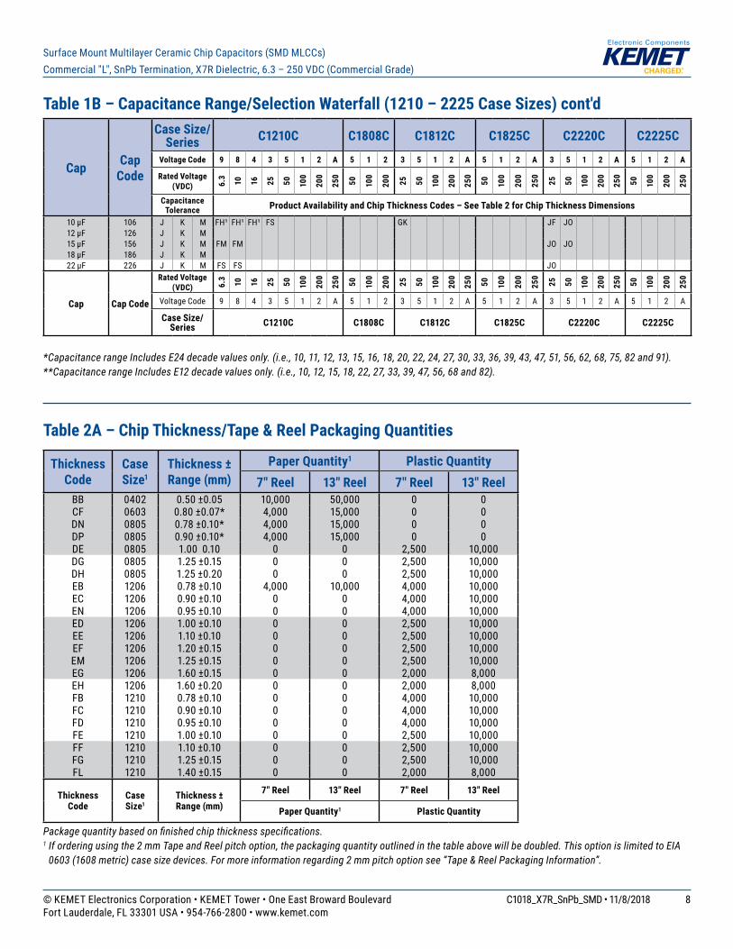
Table 1B – Capacitance Range/Selection Waterfall (1210 – 2225 Case Sizes)
*Capacitance range Includes E24 decade values only. (i.e., 10, 11, 12, 13, 15, 16, 18, 20, 22, 24, 27, 30, 33, 36, 39, 43, 47, 51, 56, 62, 68, 75, 82, and 91).**Capacitance range Includes E12 decade values only. (i.e., 10, 12, 15, 18, 22, 27, 33, 39, 47, 56, 68, and 82).
Cap Cap Code
Case Size/ Series C1210C C1808C C1812C C1825C C2220C C2225C
Voltage Code 9 8 4 3 5 1 2 A 5 1 2 3 5 1 2 A 5 1 2 A 3 5 1 2 A 5 1 2 A
Rated Voltage (VDC) 6.
3 10 16 25 50 100
200
250
50 100
200
25 50 100
200
250
50 100
200
250
25 50 100
200
250
50 100
200
250
CapacitanceTolerance Product Availability and Chip Thickness Codes – See Table 2 for Chip Thickness Dimensions
10–91pF* 100–910* J K M FB FB FB FB FB FB FB100–270pF** 101–271** J K M FB FB FB FB FB FB FB
330 pF 331 J K M FB FB FB FB FB FB FB LF LF LF390 pF 391 J K M FB FB FB FB FB FB FB LF LF LF
470–1,200pF** 471–122** J K M FB FB FB FB FB FB FB LF LF LF GB GB GB GB1,500 pF 152 J K M FB FB FB FB FB FB FE LF LF LF GB GB GB GB1,800 pF 182 J K M FB FB FB FB FB FB FE LF LF LF GB GB GB GB2,200 pF 222 J K M FB FB FB FB FB FB FB FB LF LF LF GB GB GB GB2,700 pF 272 J K M FB FB FB FB FB FB FB FB LF LF LF GB GB GB GB3,300 pF 332 J K M FB FB FB FB FB FB FB FB LF LF GB GB GB GB3,900 pF 392 J K M FB FB FB FB FB FB FB FB LF LF GB GB GB GB HB HB HB4,700 pF 472 J K M FB FB FB FB FB FB FB FB LD LD LD GB GB GB GD HB HB HB KE KE KE5,600 pF 562 J K M FB FB FB FB FB FB FB FB LD LD LD GB GB GB GH HB HB HB KE KE KE6,800 pF 682 J K M FB FB FB FB FB FB FB FB LD LD LD GB GB GB GB GB HB HB HB JE JE JE KE KE KE8,200 pF 822 J K M FB FB FB FB FB FB FB FB LD LD LD GB GB GB GB GB HB HB HB JE JE JE KE KE KE
10,000 pF 103 J K M FB FB FB FB FB FB FB FB LD LD LD GB GB GB GB GB HB HB HE JE JE JE KE KE KE12,000 pF 123 J K M FB FB FB FB FB FB FB FB LD LD LD GB GB GB GB GB HB HB HE JE JE JE KE KE KE15,000 pF 153 J K M FB FB FB FB FB FB FB FB LD LD LD GB GB GB GB GB HB HB JE JE JE KE KE KE18,000 pF 183 J K M FB FB FB FB FB FB FB FB LD LD LD GB GB GB GB GB HB HE JE JE JE KE KE22,000 pF 223 J K M FB FB FB FB FB FB FB FB LD LD GB GB GB GB GB HB HB HB HB JE JE JE KE KE27,000 pF 273 J K M FB FB FB FB FB FB FB FB LD LD GB GB GB GB GB HB HB HB HB JE JE JE KE KE33,000 pF 333 J K M FB FB FB FB FB FB FB FB LD LD GB GB GB GB GB HB HB HB HB JB JB JB KE39,000 pF 393 J K M FB FB FB FB FB FB FB FB LD LD GB GB GB GB GB HB HB HB HB JB JB JB47,000 pF 473 J K M FB FB FB FB FB FB FC FC LD LD GB GB GB GB GB HB HB HB HB JB JB JB56,000 pF 563 J K M FB FB FB FB FB FB FC FC LD LD GB GB GB GB GB HB HB HB HB JB JB JB68,000 pF 683 J K M FB FB FB FB FB FB FC FC LD GB GB GB GB GB HB HB HB HB JB JB JB82,000 pF 823 J K M FB FB FB FB FB FC FF FF LD GB GB GB GB GB HB HB HB HB JC JC JC JC JC
0.10 µF 104 J K M FB FB FB FB FB FD FG FG LD GB GB GB GB GB HB HB HB HB JC JC JC JC JC KC KC KC KC0.12 µF 124 J K M FB FB FB FB FB FD FH FH LD GB GB GB GB GB HB HB HB HB JC JC JC JC JC KC KC KC KC0.15 µF 154 J K M FC FC FC FC FC FD FM FM LD GB GB GB GE GE HB HB HB HB JC JC JC JC JC KC KC KC KC0.18 µF 184 J K M FC FC FC FC FC FD FK FK LD GB GB GB GG GG HB HB HB HB JC JC JC JC JC KC KC KC KC0.22 µF 224 J K M FC FC FC FC FC FD FK FK GB GB GB GG GG HB HB HB HB JC JC JC JC JC KC KC KC KC0.27 µF 274 J K M FC FC FC FC FC FD FP FP GB GB GG GG GG HB HB HB HB JC JC JC JC JC KB KC KC KC0.33 µF 334 J K M FD FD FD FD FD FD FM FM GB GB GG GG GG HB HB HB HB JC JC JC JC JC KB KC KC KC0.39 µF 394 J K M FD FD FD FD FD FD FK FK GB GB GG GG GG HB HB HD HD JC JC JC JC JC KB KC KC KC0.47 µF 474 J K M FD FD FD FD FD FD FS FS GB GB GG GJ GJ HB HB HD HD JC JC JC JC JC KB KC KD KD0.56 µF 564 J K M FD FD FD FD FD FF GC GC GG HB HD HD HD JC JC JC JD JD KB KC KD KD0.68 µF 684 J K M FD FD FD FD FD FG GC GC GG HB HD HD HD JC JC JD JD JD KB KC KD KD0.82 µF 824 J K M FF FF FF FF FF FL GE GE GG HB HF HF HF JC JC JF JF JF KB KC KE KE1.0 µF 105 J K M FH FH FH FH FH FM GE GE GG HB HF HF HF JC JC JF JF JF KB KD KE KE1.2 µF 125 J K M FH FH FH FH FG FH GB GB GB HB JC JC KB KE KE KE1.5 µF 155 J K M FH FH FH FH FG FM GC GC GC HC JC JC KC1.8 µF 185 J K M FH FH FH FH FG FJ GE GE GE HD JD JD KD2.2 µF 225 J K M FJ FJ FJ FJ FG FK GO GO GG HF JF JF KD2.7 µF 275 J K M FE FE FE FG FH GJ GJ GJ3.3 µF 335 J K M FF FF FF FM FM GL GL GL3.9 µF 395 J K M FG FG FG FG FK4.7 µF 475 J K M FC FC FC FG FS GK GK JF JF5.6 µF 565 J K M FF FF FF FH6.8 µF 685 J K M FG FG FG FM8.2 µF 825 J K M FH FH FH FK
Cap Cap Code
Rated Voltage (VDC) 6.3 10 16 25 50 100
200
250
50 100
200
25 50 100
200
250
50 100
200
250
25 50 100
200
250
50 100
200
250
VoltageCode 9 8 4 3 5 1 2 A 5 1 2 3 5 1 2 A 5 1 2 A 3 5 1 2 A 5 1 2 A
Case Size/ Series C1210C C1808C C1812C C1825C C2220C C2225C
8© KEMET Electronics Corporation • KEMET Tower • One East Broward Boulevard C1018_X7R_SnPb_SMD • 11/8/2018Fort Lauderdale, FL 33301 USA • 954-766-2800 • www.kemet.com
Surface Mount Multilayer Ceramic Chip Capacitors (SMD MLCCs)Commercial "L", SnPb Termination, X7R Dielectric, 6.3 – 250 VDC (Commercial Grade)
Table 1B – Capacitance Range/Selection Waterfall (1210 – 2225 Case Sizes) cont'd
*Capacitance range Includes E24 decade values only. (i.e., 10, 11, 12, 13, 15, 16, 18, 20, 22, 24, 27, 30, 33, 36, 39, 43, 47, 51, 56, 62, 68, 75, 82 and 91).**Capacitance range Includes E12 decade values only. (i.e., 10, 12, 15, 18, 22, 27, 33, 39, 47, 56, 68 and 82).
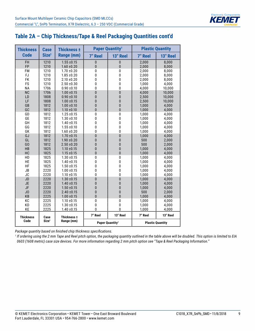
Table 2A – Chip Thickness/Tape & Reel Packaging Quantities
Package quantity based on finished chip thickness specifications.1 If ordering using the 2 mm Tape and Reel pitch option, the packaging quantity outlined in the table above will be doubled. This option is limited to EIA
0603 (1608 metric) case size devices. For more information regarding 2 mm pitch option see “Tape & Reel Packaging Information”.
Cap Cap Code
Case Size/ Series C1210C C1808C C1812C C1825C C2220C C2225C
Voltage Code 9 8 4 3 5 1 2 A 5 1 2 3 5 1 2 A 5 1 2 A 3 5 1 2 A 5 1 2 A
Rated Voltage (VDC) 6.
3 10 16 25 50 100
200
250
50 100
200
25 50 100
200
250
50 100
200
250
25 50 100
200
250
50 100
200
250
CapacitanceTolerance Product Availability and Chip Thickness Codes – See Table 2 for Chip Thickness Dimensions
10 µF 106 J K M FH¹ FH¹ FH¹ FS GK JF JO12 µF 126 J K M15 µF 156 J K M FM FM JO JO18 µF 186 J K M22 µF 226 J K M FS FS JO
Cap Cap Code
Rated Voltage (VDC) 6.
3 10 16 25 50 100
200
250
50 100
200
25 50 100
200
250
50 100
200
250
25 50 100
200
250
50 100
200
250
VoltageCode 9 8 4 3 5 1 2 A 5 1 2 3 5 1 2 A 5 1 2 A 3 5 1 2 A 5 1 2 A
Case Size/ Series C1210C C1808C C1812C C1825C C2220C C2225C
Thickness Code
Case Size1
Thickness ± Range (mm)
Paper Quantity1 Plastic Quantity7" Reel 13" Reel 7" Reel 13" Reel
BB 0402 0.50±0.05 10,000 50,000 0 0 CF 0603 0.80±0.07* 4,000 15,000 0 0 DN 0805 0.78±0.10* 4,000 15,000 0 0 DP 0805 0.90±0.10* 4,000 15,000 0 0 DE 0805 1.00 0.10 0 0 2,500 10,000 DG 0805 1.25±0.15 0 0 2,500 10,000 DH 0805 1.25±0.20 0 0 2,500 10,000 EB 1206 0.78±0.10 4,000 10,000 4,000 10,000 EC 1206 0.90±0.10 0 0 4,000 10,000 EN 1206 0.95±0.10 0 0 4,000 10,000 ED 1206 1.00±0.10 0 0 2,500 10,000 EE 1206 1.10±0.10 0 0 2,500 10,000 EF 1206 1.20±0.15 0 0 2,500 10,000 EM 1206 1.25±0.15 0 0 2,500 10,000 EG 1206 1.60±0.15 0 0 2,000 8,000 EH 1206 1.60±0.20 0 0 2,000 8,000 FB 1210 0.78±0.10 0 0 4,000 10,000 FC 1210 0.90±0.10 0 0 4,000 10,000 FD 1210 0.95±0.10 0 0 4,000 10,000 FE 1210 1.00±0.10 0 0 2,500 10,000 FF 1210 1.10±0.10 0 0 2,500 10,000 FG 1210 1.25±0.15 0 0 2,500 10,000 FL 1210 1.40±0.15 0 0 2,000 8,000
Thickness Code
Case Size1
Thickness ± Range (mm)
7" Reel 13" Reel 7" Reel 13" Reel
Paper Quantity1 Plastic Quantity
9© KEMET Electronics Corporation • KEMET Tower • One East Broward Boulevard C1018_X7R_SnPb_SMD • 11/8/2018Fort Lauderdale, FL 33301 USA • 954-766-2800 • www.kemet.com
Surface Mount Multilayer Ceramic Chip Capacitors (SMD MLCCs)Commercial "L", SnPb Termination, X7R Dielectric, 6.3 – 250 VDC (Commercial Grade)
Table 2A – Chip Thickness/Tape & Reel Packaging Quantities cont'd
Package quantity based on finished chip thickness specifications.1 If ordering using the 2 mm Tape and Reel pitch option, the packaging quantity outlined in the table above will be doubled. This option is limited to EIA
0603 (1608 metric) case size devices. For more information regarding 2 mm pitch option see “Tape & Reel Packaging Information.”
Thickness Code
Case Size1
Thickness ± Range (mm)
Paper Quantity1 Plastic Quantity7" Reel 13" Reel 7" Reel 13" Reel
FH 1210 1.55±0.15 0 0 2,000 8,000 FP 1210 1.60±0.20 0 0 2,000 8,000 FM 1210 1.70±0.20 0 0 2,000 8,000 FJ 1210 1.85±0.20 0 0 2,000 8,000 FK 1210 2.10±0.20 0 0 2,000 8,000 FS 1210 2.50±0.30 0 0 1,000 4,000 NA 1706 0.90±0.10 0 0 4,000 10,000 NC 1706 1.00±0.15 0 0 4,000 10,000 LD 1808 0.90±0.10 0 0 2,500 10,000 LF 1808 1.00±0.15 0 0 2,500 10,000 GB 1812 1.00±0.10 0 0 1,000 4,000 GC 1812 1.10±0.10 0 0 1,000 4,000 GD 1812 1.25±0.15 0 0 1,000 4,000 GE 1812 1.30±0.10 0 0 1,000 4,000 GH 1812 1.40±0.15 0 0 1,000 4,000 GG 1812 1.55±0.10 0 0 1,000 4,000 GK 1812 1.60±0.20 0 0 1,000 4,000 GJ 1812 1.70±0.15 0 0 1,000 4,000 GL 1812 1.90±0.20 0 0 500 2,000 GO 1812 2.50±0.20 0 0 500 2,000 HB 1825 1.10±0.15 0 0 1,000 4,000 HC 1825 1.15±0.15 0 0 1,000 4,000 HD 1825 1.30±0.15 0 0 1,000 4,000 HE 1825 1.40±0.15 0 0 1,000 4,000 HF 1825 1.50±0.15 0 0 1,000 4,000 JB 2220 1.00±0.15 0 0 1,000 4,000 JC 2220 1.10±0.15 0 0 1,000 4,000 JD 2220 1.30±0.15 0 0 1,000 4,000 JE 2220 1.40±0.15 0 0 1,000 4,000 JF 2220 1.50±0.15 0 0 1,000 4,000 JO 2220 2.40±0.15 0 0 500 2,000 KB 2225 1.00±0.15 0 0 1,000 4,000 KC 2225 1.10±0.15 0 0 1,000 4,000 KD 2225 1.30±0.15 0 0 1,000 4,000 KE 2225 1.40±0.15 0 0 1,000 4,000
Thickness Code
Case Size1
Thickness ± Range (mm)
7" Reel 13" Reel 7" Reel 13" Reel
Paper Quantity1 Plastic Quantity
10© KEMET Electronics Corporation • KEMET Tower • One East Broward Boulevard C1018_X7R_SnPb_SMD • 11/8/2018Fort Lauderdale, FL 33301 USA • 954-766-2800 • www.kemet.com
Surface Mount Multilayer Ceramic Chip Capacitors (SMD MLCCs)Commercial "L", SnPb Termination, X7R Dielectric, 6.3 – 250 VDC (Commercial Grade)
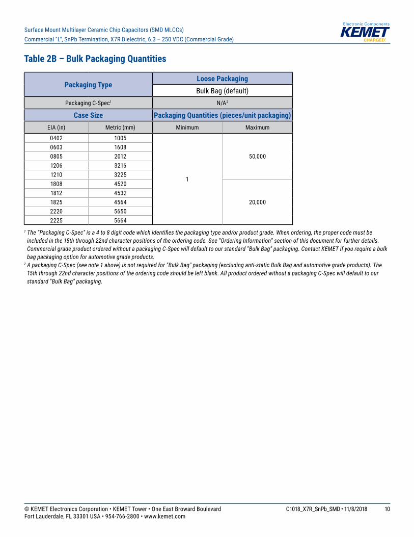
Table 2B – Bulk Packaging Quantities
Packaging TypeLoose PackagingBulkBag(default)
PackagingC-Spec1 N/A2
Case Size Packaging Quantities (pieces/unit packaging)EIA(in) Metric(mm) Minimum Maximum
0402 1005
1
50,0000603 16080805 20121206 32161210 32251808 4520
20,0001812 45321825 45642220 56502225 5664
1 The "Packaging C-Spec" is a 4 to 8 digit code which identifies the packaging type and/or product grade. When ordering, the proper code must be included in the 15th through 22nd character positions of the ordering code. See "Ordering Information" section of this document for further details. Commercial grade product ordered without a packaging C-Spec will default to our standard "Bulk Bag" packaging. Contact KEMET if you require a bulk bag packaging option for automotive grade products.
2 A packaging C-Spec (see note 1 above) is not required for "Bulk Bag" packaging (excluding anti-static Bulk Bag and automotive grade products). The 15th through 22nd character positions of the ordering code should be left blank. All product ordered without a packaging C-Spec will default to our standard "Bulk Bag" packaging.
11© KEMET Electronics Corporation • KEMET Tower • One East Broward Boulevard C1018_X7R_SnPb_SMD • 11/8/2018Fort Lauderdale, FL 33301 USA • 954-766-2800 • www.kemet.com
Surface Mount Multilayer Ceramic Chip Capacitors (SMD MLCCs)Commercial "L", SnPb Termination, X7R Dielectric, 6.3 – 250 VDC (Commercial Grade)
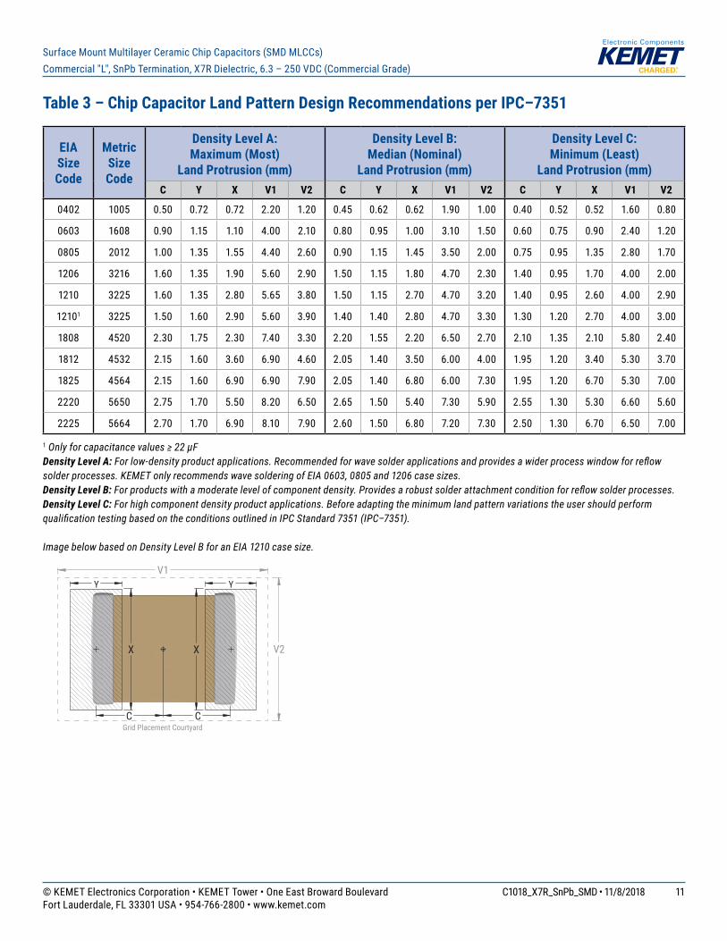
Table 3 – Chip Capacitor Land Pattern Design Recommendations per IPC–7351
EIA Size Code
Metric Size Code
Density Level A: Maximum (Most)
Land Protrusion (mm)
Density Level B: Median (Nominal)
Land Protrusion (mm)
Density Level C: Minimum (Least)
Land Protrusion (mm)C Y X V1 V2 C Y X V1 V2 C Y X V1 V2
0402 1005 0.50 0.72 0.72 2.20 1.20 0.45 0.62 0.62 1.90 1.00 0.40 0.52 0.52 1.60 0.80
0603 1608 0.90 1.15 1.10 4.00 2.10 0.80 0.95 1.00 3.10 1.50 0.60 0.75 0.90 2.40 1.20
0805 2012 1.00 1.35 1.55 4.40 2.60 0.90 1.15 1.45 3.50 2.00 0.75 0.95 1.35 2.80 1.70
1206 3216 1.60 1.35 1.90 5.60 2.90 1.50 1.15 1.80 4.70 2.30 1.40 0.95 1.70 4.00 2.00
1210 3225 1.60 1.35 2.80 5.65 3.80 1.50 1.15 2.70 4.70 3.20 1.40 0.95 2.60 4.00 2.90
12101 3225 1.50 1.60 2.90 5.60 3.90 1.40 1.40 2.80 4.70 3.30 1.30 1.20 2.70 4.00 3.00
1808 4520 2.30 1.75 2.30 7.40 3.30 2.20 1.55 2.20 6.50 2.70 2.10 1.35 2.10 5.80 2.40
1812 4532 2.15 1.60 3.60 6.90 4.60 2.05 1.40 3.50 6.00 4.00 1.95 1.20 3.40 5.30 3.70
1825 4564 2.15 1.60 6.90 6.90 7.90 2.05 1.40 6.80 6.00 7.30 1.95 1.20 6.70 5.30 7.00
2220 5650 2.75 1.70 5.50 8.20 6.50 2.65 1.50 5.40 7.30 5.90 2.55 1.30 5.30 6.60 5.60
2225 5664 2.70 1.70 6.90 8.10 7.90 2.60 1.50 6.80 7.20 7.30 2.50 1.30 6.70 6.50 7.00
1 Only for capacitance values ≥ 22 µFDensity Level A: For low-density product applications. Recommended for wave solder applications and provides a wider process window for reflow solder processes. KEMET only recommends wave soldering of EIA 0603, 0805 and 1206 case sizes.Density Level B: For products with a moderate level of component density. Provides a robust solder attachment condition for reflow solder processes.Density Level C: For high component density product applications. Before adapting the minimum land pattern variations the user should perform qualification testing based on the conditions outlined in IPC Standard 7351 (IPC–7351).
Image below based on Density Level B for an EIA 1210 case size.
Y
C C
X X
V1
V2
Grid Placement Courtyard
Y
12© KEMET Electronics Corporation • KEMET Tower • One East Broward Boulevard C1018_X7R_SnPb_SMD • 11/8/2018Fort Lauderdale, FL 33301 USA • 954-766-2800 • www.kemet.com
Surface Mount Multilayer Ceramic Chip Capacitors (SMD MLCCs)Commercial "L", SnPb Termination, X7R Dielectric, 6.3 – 250 VDC (Commercial Grade)
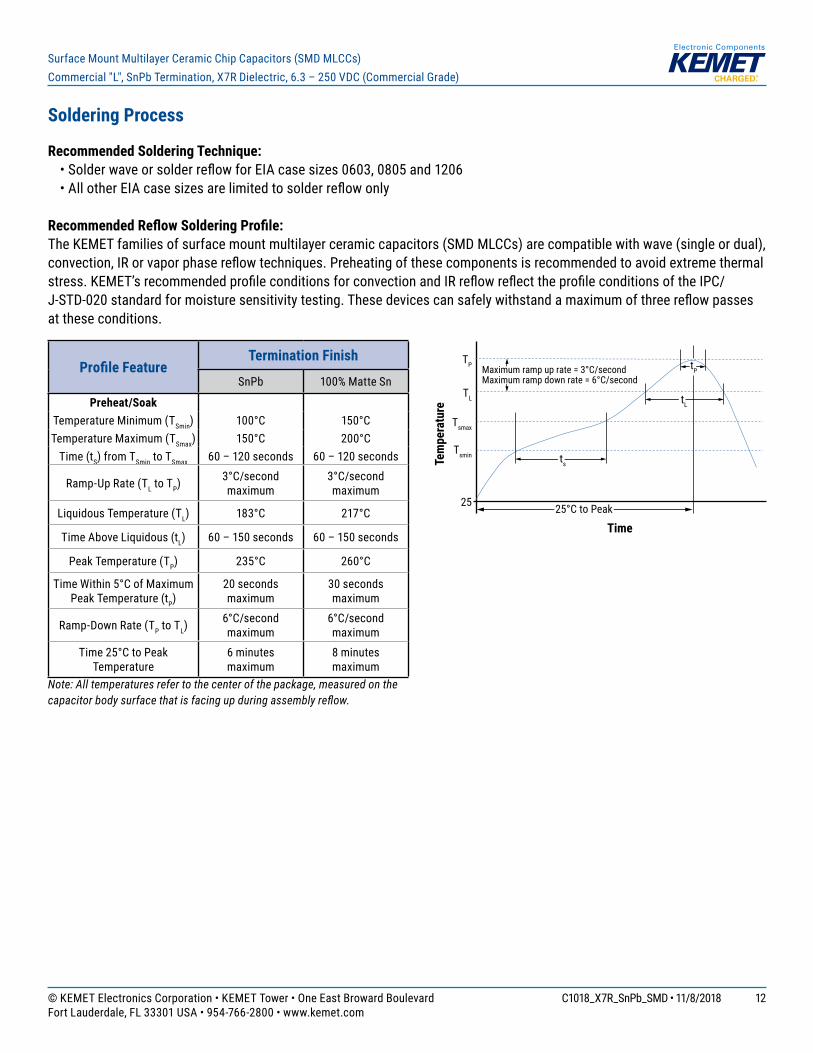
Soldering Process
Recommended Soldering Technique: •SolderwaveorsolderreflowforEIAcasesizes0603,0805and1206 •AllotherEIAcasesizesarelimitedtosolderreflowonly
Recommended Reflow Soldering Profile:TheKEMETfamiliesofsurfacemountmultilayerceramiccapacitors(SMDMLCCs)arecompatiblewithwave(singleordual),convection,IRorvaporphasereflowtechniques.Preheatingofthesecomponentsisrecommendedtoavoidextremethermalstress.KEMET’srecommendedprofileconditionsforconvectionandIRreflowreflecttheprofileconditionsoftheIPC/J-STD-020standardformoisturesensitivitytesting.Thesedevicescansafelywithstandamaximumofthreereflowpassesattheseconditions.
Profile FeatureTermination Finish
SnPb 100%MatteSn
Preheat/SoakTemperatureMinimum(TSmin) 100°C 150°CTemperatureMaximum(TSmax) 150°C 200°CTime(tS)fromTSmin to TSmax 60–120seconds 60–120seconds
Ramp-UpRate(TL to TP)3°C/secondmaximum
3°C/secondmaximum
LiquidousTemperature(TL) 183°C 217°C
TimeAboveLiquidous(tL) 60–150seconds 60–150seconds
PeakTemperature(TP) 235°C 260°C
TimeWithin5°CofMaximumPeakTemperature(tP)
20 seconds maximum
30 seconds maximum
Ramp-DownRate(TP to TL)6°C/secondmaximum
6°C/secondmaximum
Time25°CtoPeakTemperature
6 minutes maximum
8 minutes maximum
Note: All temperatures refer to the center of the package, measured on the capacitor body surface that is facing up during assembly reflow.
Time
Tem
pera
ture
Tsmin
25
Tsmax
TL
TP Maximum ramp up rate = 3°C/secondMaximum ramp down rate = 6°C/second
tP
tL
ts
25°C to Peak
13© KEMET Electronics Corporation • KEMET Tower • One East Broward Boulevard C1018_X7R_SnPb_SMD • 11/8/2018Fort Lauderdale, FL 33301 USA • 954-766-2800 • www.kemet.com
Surface Mount Multilayer Ceramic Chip Capacitors (SMD MLCCs)Commercial "L", SnPb Termination, X7R Dielectric, 6.3 – 250 VDC (Commercial Grade)
Table 4 – Performance & Reliability: Test Methods and Conditions
Stress Reference Test or Inspection MethodTerminalStrength JIS–C–6429 Appendix1,Note:Forceof1.8kgfor60seconds.
Board Flex JIS–C–6429 Appendix2,Note:Standardterminationsystem–2.0mm(minimum)forallexcept3mmforC0G.Flexibleterminationsystem–3.0mm(minimum).
Solderability J–STD–002
Magnification50X,conditions:
a)MethodB,4hoursat155°C,dryheatat235°C
b)MethodB,category3at215°C
c)MethodD,category3at260°C
TemperatureCycling JESD22MethodJA–104 1,000Cycles(−55°Cto+125°C).Measurementat24hours±4hoursaftertestconclusion.
Biased Humidity MIL–STD–202 Method103
Loadhumidity:1,000hours85°C/85%RHandratedvoltage.Add100Kohmresistor.Measurementat24hours±4hoursaftertestconclusion.Lowvolthumidity:1,000hours85°C/85%RHand1.5V.Add100Kohmresistor.Measurementat24hours±4hoursaftertestconclusion.
Moisture Resistance MIL–STD–202 Method106
t=24hours/cycle.Steps7aand7bnotrequired.Measurementat24hours±4hoursaftertestconclusion.
ThermalShock MIL–STD–202 Method107
−55°C/+125°C.Note:Numberofcyclesrequired–300.Maximumtransfertime–20seconds.Dwelltime–15minutes.Air–air.
HighTemperatureLife MIL–STD–202 Method108/EIA–198 1,000hoursat125°C(85°CforX5R,Z5UandY5V)with2Xratedvoltageapplied.
StorageLife MIL–STD–202 Method108 150°C,0VDCfor1,000hours.
Vibration MIL–STD–202 Method204
5g'sfor20minutes,12cycleseachof3orientations.Note:Use8"X5"PCB0.031"thick7securepointsononelongsideand2securepointsatcornersofoppositesides.Partsmountedwithin2"fromanysecurepoint.Testfrom10–2,000Hz
MechanicalShock MIL–STD–202 Method213 Figure1ofMethod213,ConditionF.
Resistance to Solvents MIL–STD–202 Method215 Addaqueouswashchemical,OKEMCleanorequivalent.
Storage & Handling
Ceramicchipcapacitorsshouldbestoredinnormalworkingenvironments.Whilethechipsthemselvesarequiterobustinotherenvironments,solderabilitywillbedegradedbyexposuretohightemperatures,highhumidity,corrosiveatmospheres,andlongtermstorage.Inaddition,packagingmaterialswillbedegradedbyhightemperature–reelsmaysoftenorwarpandtapepeelforcemayincrease.KEMETrecommendsthatmaximumstoragetemperaturenotexceed40°Candmaximumstoragehumiditynotexceed70%relativehumidity.Temperaturefluctuationsshouldbeminimizedtoavoidcondensationonthepartsandatmospheresshouldbefreeofchlorineandsulfurbearingcompounds.Foroptimizedsolderabilitychipstockshouldbeusedpromptly,preferablywithin1.5yearsofreceipt.
14© KEMET Electronics Corporation • KEMET Tower • One East Broward Boulevard C1018_X7R_SnPb_SMD • 11/8/2018Fort Lauderdale, FL 33301 USA • 954-766-2800 • www.kemet.com
Surface Mount Multilayer Ceramic Chip Capacitors (SMD MLCCs)Commercial "L", SnPb Termination, X7R Dielectric, 6.3 – 250 VDC (Commercial Grade)
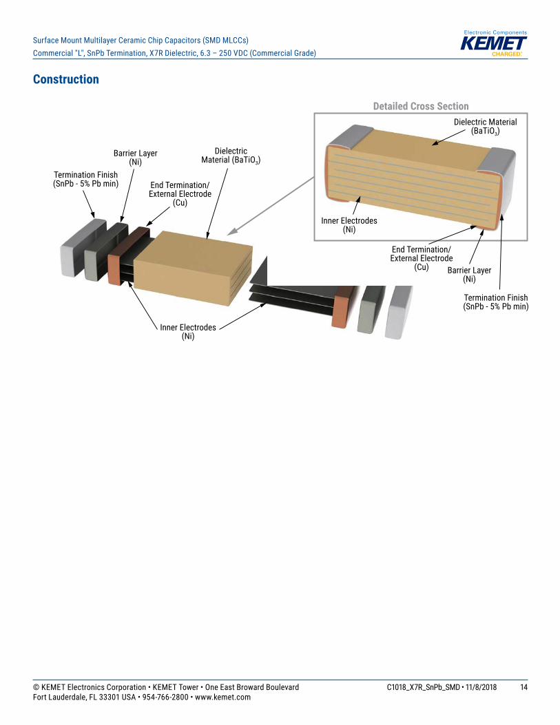
Construction
Dielectric Material (BaTiO3)
Detailed Cross Section
Barrier Layer(Ni)
Inner Electrodes(Ni)
Barrier Layer(Ni)
Inner Electrodes(Ni)
Dielectric Material (BaTiO3)
Termination Finish(SnPb - 5% Pb min)
Termination Finish(SnPb - 5% Pb min) End Termination/
External Electrode (Cu)
End Termination/External Electrode
(Cu)
15© KEMET Electronics Corporation • KEMET Tower • One East Broward Boulevard C1018_X7R_SnPb_SMD • 11/8/2018Fort Lauderdale, FL 33301 USA • 954-766-2800 • www.kemet.com
Surface Mount Multilayer Ceramic Chip Capacitors (SMD MLCCs)Commercial "L", SnPb Termination, X7R Dielectric, 6.3 – 250 VDC (Commercial Grade)
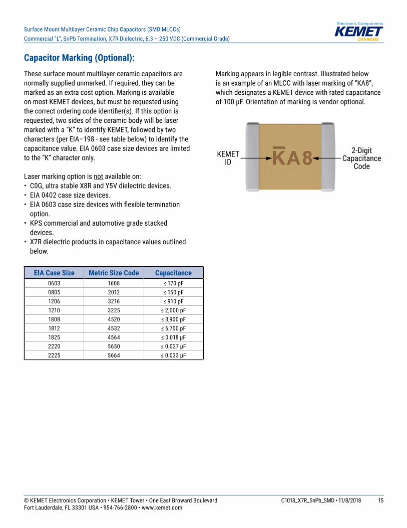
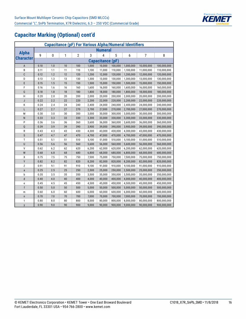
Capacitor Marking (Optional):Thesesurfacemountmultilayerceramiccapacitorsarenormallysuppliedunmarked.Ifrequired,theycanbemarkedasanextracostoption.MarkingisavailableonmostKEMETdevices,butmustberequestedusingthecorrectorderingcodeidentifier(s).Ifthisoptionisrequested,twosidesoftheceramicbodywillbelasermarkedwitha“K”toidentifyKEMET,followedbytwocharacters(perEIA–198-seetablebelow)toidentifythecapacitance value. EIA 0603 case size devices are limited tothe“K”characteronly.
Lasermarkingoptionisnot available on:• C0G,ultrastableX8RandY5Vdielectricdevices.• EIA 0402 case size devices. • EIA0603casesizedeviceswithflexibletermination
option.• KPScommercialandautomotivegradestacked
devices.• X7R dielectric products in capacitance values outlined
below.
Markingappearsinlegiblecontrast.IllustratedbelowisanexampleofanMLCCwithlasermarkingof“KA8”,whichdesignatesaKEMETdevicewithratedcapacitanceof100µF.Orientationofmarkingisvendoroptional.
KEMET ID
2-Digit Capacitance
Code
EIA Case Size Metric Size Code Capacitance0603 1608 ≤170pF0805 2012 ≤150pF1206 3216 ≤910pF1210 3225 ≤2,000pF1808 4520 ≤3,900pF1812 4532 ≤6,700pF1825 4564 ≤0.018µF2220 5650 ≤0.027µF2225 5664 ≤0.033µF
16© KEMET Electronics Corporation • KEMET Tower • One East Broward Boulevard C1018_X7R_SnPb_SMD • 11/8/2018Fort Lauderdale, FL 33301 USA • 954-766-2800 • www.kemet.com
Surface Mount Multilayer Ceramic Chip Capacitors (SMD MLCCs)Commercial "L", SnPb Termination, X7R Dielectric, 6.3 – 250 VDC (Commercial Grade)
Capacitor Marking (Optional) cont’dCapacitance (pF) For Various Alpha/Numeral Identifi ers
AlphaCharacter
Numeral9 0 1 2 3 4 5 6 7 8
Capacitance (pF)A 0.10 1.0 10 100 1,000 10,000 100,000 1,000,000 10,000,000 100,000,000B 0.11 1.1 11 110 1,100 11,000 110,000 1,100,000 11,000,000 110,000,000C 0.12 1.2 12 120 1,200 12,000 120,000 1,200,000 12,000,000 120,000,000D 0.13 1.3 13 130 1,300 13,000 130,000 1,300,000 13,000,000 130,000,000E 0.15 1.5 15 150 1,500 15,000 150,000 1,500,000 15,000,000 150,000,000F 0.16 1.6 16 160 1,600 16,000 160,000 1,600,000 16,000,000 160,000,000G 0.18 1.8 18 180 1,800 18,000 180,000 1,800,000 18,000,000 180,000,000H 0.20 2.0 20 200 2,000 20,000 200,000 2,000,000 20,000,000 200,000,000J 0.22 2.2 22 220 2,200 22,000 220,000 2,200,000 22,000,000 220,000,000K 0.24 2.4 24 240 2,400 24,000 240,000 2,400,000 24,000,000 240,000,000L 0.27 2.7 27 270 2,700 27,000 270,000 2,700,000 27,000,000 270,000,000M 0.30 3.0 30 300 3,000 30,000 300,000 3,000,000 30,000,000 300,000,000N 0.33 3.3 33 330 3,300 33,000 330,000 3,300,000 33,000,000 330,000,000P 0.36 3.6 36 360 3,600 36,000 360,000 3,600,000 36,000,000 360,000,000Q 0.39 3.9 39 390 3,900 39,000 390,000 3,900,000 39,000,000 390,000,000R 0.43 4.3 43 430 4,300 43,000 430,000 4,300,000 43,000,000 430,000,000S 0.47 4.7 47 470 4,700 47,000 470,000 4,700,000 47,000,000 470,000,000T 0.51 5.1 51 510 5,100 51,000 510,000 5,100,000 51,000,000 510,000,000U 0.56 5.6 56 560 5,600 56,000 560,000 5,600,000 56,000,000 560,000,000V 0.62 6.2 62 620 6,200 62,000 620,000 6,200,000 62,000,000 620,000,000W 0.68 6.8 68 680 6,800 68,000 680,000 6,800,000 68,000,000 680,000,000X 0.75 7.5 75 750 7,500 75,000 750,000 7,500,000 75,000,000 750,000,000Y 0.82 8.2 82 820 8,200 82,000 820,000 8,200,000 82,000,000 820,000,000Z 0.91 9.1 91 910 9,100 91,000 910,000 9,100,000 91,000,000 910,000,000a 0.25 2.5 25 250 2,500 25,000 250,000 2,500,000 25,000,000 250,000,000b 0.35 3.5 35 350 3,500 35,000 350,000 3,500,000 35,000,000 350,000,000d 0.40 4.0 40 400 4,000 40,000 400,000 4,000,000 40,000,000 400,000,000e 0.45 4.5 45 450 4,500 45,000 450,000 4,500,000 45,000,000 450,000,000f 0.50 5.0 50 500 5,000 50,000 500,000 5,000,000 50,000,000 500,000,000m 0.60 6.0 60 600 6,000 60,000 600,000 6,000,000 60,000,000 600,000,000n 0.70 7.0 70 700 7,000 70,000 700,000 7,000,000 70,000,000 700,000,000t 0.80 8.0 80 800 8,000 80,000 800,000 8,000,000 80,000,000 800,000,000y 0.90 9.0 90 900 9,000 90,000 900,000 9,000,000 90,000,000 900,000,000
17© KEMET Electronics Corporation • KEMET Tower • One East Broward Boulevard C1018_X7R_SnPb_SMD • 11/8/2018Fort Lauderdale, FL 33301 USA • 954-766-2800 • www.kemet.com
Surface Mount Multilayer Ceramic Chip Capacitors (SMD MLCCs)Commercial "L", SnPb Termination, X7R Dielectric, 6.3 – 250 VDC (Commercial Grade)
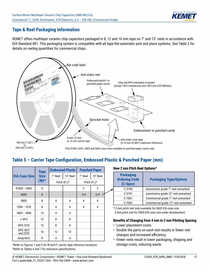
Tape & Reel Packaging Information
KEMEToffersmultilayerceramicchipcapacitorspackagedin8,12and16mmtapeon7"and13"reelsinaccordancewithEIAStandard481.Thispackagingsystemiscompatiblewithalltape-fedautomaticpickandplacesystems.SeeTable2fordetailsonreelingquantitiesforcommercialchips.
8 mm, 12 mmor 16 mm carrier tape 180 mm (7.00")
or330 mm (13.00")
Anti-static reel
Embossed plastic* or punched paper carrier.
Embossment or punched cavity
Anti-static cover tape(0.10 mm (0.004") maximum thickness)
Chip and KPS orientation in pocket(except 1825 commercial, and 1825 and 2225 Military)
*EIA 01005, 0201, 0402 and 0603 case sizes available on punched paper carrier only.
KEMET®
Bar code label
Sprocket holes
Table 5 – Carrier Tape Confi guration, Embossed Plastic & Punched Paper (mm)
EIA Case SizeTape Size (W)*
Embossed Plastic Punched Paper7"Reel 13"Reel 7"Reel 13"Reel
Pitch(P1)* Pitch(P1)*
01005–0402 8 2 2
0603 8 2/4 2/4
0805 8 4 4 4 4
1206–1210 8 4 4 4 4
1805–1808 12 4 4
≥1812 12 8 8
KPS 1210 12 8 8KPS 1812and 2220 16 12 12
Array 0612 8 4 4
*Refer to Figures 1 and 2 for W and P1 carrier tape reference locations.*Refer to Tables 6 and 7 for tolerance specifi cations.
New 2 mm Pitch Reel Options*
PackagingOrdering Code
(C-Spec)Packaging Type/Options
C-3190 Automotivegrade7"reelunmarkedC-3191 Automotivegrade13"reelunmarkedC-7081 Commercialgrade7"reelunmarkedC-7082 Commercialgrade13"reelunmarked
* 2 mm pitch reel only available for 0603 EIA case size. 2 mm pitch reel for 0805 EIA case size under development.
Benefi ts of Changing from 4 mm to 2 mm Pitching Spacing• Lower placement costs.• Doublethepartsoneachreelresultsinfewerreelchangesandincreasedefficiency.
• Fewerreelsresultinlowerpackaging,shippingandstoragecosts,reducingwaste.
18© KEMET Electronics Corporation • KEMET Tower • One East Broward Boulevard C1018_X7R_SnPb_SMD • 11/8/2018Fort Lauderdale, FL 33301 USA • 954-766-2800 • www.kemet.com
Surface Mount Multilayer Ceramic Chip Capacitors (SMD MLCCs)Commercial "L", SnPb Termination, X7R Dielectric, 6.3 – 250 VDC (Commercial Grade)
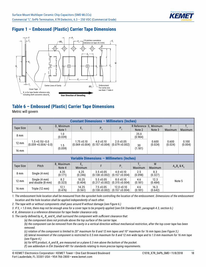
Figure 1 – Embossed (Plastic) Carrier Tape Dimensions
P0
T
F
W
Center Lines of Cavity
A0
B0
User Direction of Unreeling
Cover Tape
K0
B1 is for tape feeder reference only, including draft concentric about B0.
T2
ØD1
ØD0
B1
S1
T1
E1
E2
P1
P2
EmbossmentFor cavity size,see Note 1 Table 4
(10 pitches cumulativetolerance on tape ±0.2 mm)
Table 6 – Embossed (Plastic) Carrier Tape DimensionsMetricwillgovern
Constant Dimensions — Millimeters (Inches)
Tape Size D0 D1 Minimum
Note 1 E1 P0 P2 RReference
Note 2S1 Minimum
Note 3T
MaximumT1
Maximum
8 mm
1.5+0.10/−0.0(0.059+0.004/−0.0)
1.0 (0.039)
1.75±0.10(0.069±0.004)
4.0±0.10(0.157±0.004)
2.0±0.05(0.079±0.002)
25.0 (0.984)
0.600 (0.024)
0.600 (0.024)
0.100 (0.004)12 mm
1.5 (0.059)
30 (1.181)
16 mm
Variable Dimensions — Millimeters (Inches)
Tape Size Pitch B1 MaximumNote 4
E2 Minimum F P1
T2 Maximum
WMaximum A0,B0&K0
8 mm Single(4mm) 4.35 (0.171)
6.25 (0.246)
3.5±0.05(0.138±0.002)
4.0±0.10(0.157±0.004)
2.5 (0.098)
8.3 (0.327)
Note 512 mm Single(4mm)anddouble(8mm)
8.2 (0.323)
10.25 (0.404)
5.5±0.05(0.217±0.002)
8.0±0.10(0.315±0.004)
4.6 (0.181)
12.3 (0.484)
16 mm Triple(12mm) 12.1 (0.476)
14.25(0.561)
7.5±0.05(0.138±0.002)
12.0±0.10(0.157±0.004)
4.6 (0.181)
16.3 (0.642)
1. The embossment hole location shall be measured from the sprocket hole controlling the location of the embossment. Dimensions of the embossment location and the hole location shall be applied independently of each other.
2. The tape with or without components shall pass around R without damage (see Figure 6.)3. If S1 < 1.0 mm, there may not be enough area for a cover tape to be properly applied (see EIA Standard 481, paragraph 4.3, section b.)4. B1 dimension is a reference dimension for tape feeder clearance only.5. The cavity defi ned by A0, B0 and K0 shall surround the component with suffi cient clearance that: (a) the component does not protrude above the top surface of the carrier tape. (b) the component can be removed from the cavity in a vertical direction without mechanical restriction, after the top cover tape has been
removed. (c) rotation of the component is limited to 20° maximum for 8 and 12 mm tapes and 10° maximum for 16 mm tapes (see Figure 3.) (d) lateral movement of the component is restricted to 0.5 mm maximum for 8 and 12 mm wide tape and to 1.0 mm maximum for 16 mm tape
(see Figure 4.) (e) for KPS product, A0 and B0 are measured on a plane 0.3 mm above the bottom of the pocket. (f) see addendum in EIA Standard 481 for standards relating to more precise taping requirements.
19© KEMET Electronics Corporation • KEMET Tower • One East Broward Boulevard C1018_X7R_SnPb_SMD • 11/8/2018Fort Lauderdale, FL 33301 USA • 954-766-2800 • www.kemet.com
Surface Mount Multilayer Ceramic Chip Capacitors (SMD MLCCs)Commercial "L", SnPb Termination, X7R Dielectric, 6.3 – 250 VDC (Commercial Grade)
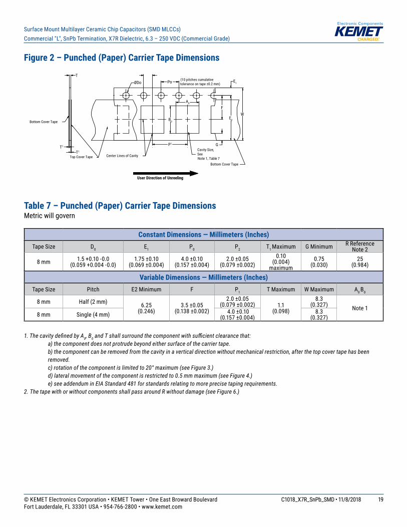
Figure 2 – Punched (Paper) Carrier Tape Dimensions
User Direction of Unreeling
Top Cover Tape
T
Center Lines of Cavity
P1
ØDo Po E1
F
E2
W
G
A0
B0
Cavity Size,SeeNote 1, Table 7
Bottom Cover Tape
T1
T1
Bottom Cover Tape
(10 pitches cumulativetolerance on tape ±0.2 mm)
Table 7 – Punched (Paper) Carrier Tape Dimensions Metricwillgovern
Constant Dimensions — Millimeters (Inches)Tape Size D0 E1 P0 P2 T1 Maximum GMinimum RReference
Note 2
8 mm 1.5+0.10-0.0(0.059+0.004-0.0)
1.75±0.10(0.069±0.004)
4.0±0.10(0.157±0.004)
2.0±0.05(0.079±0.002)
0.10 (0.004)
maximum0.75
(0.030)25
(0.984)
Variable Dimensions — Millimeters (Inches)Tape Size Pitch E2 Minimum F P1 T Maximum WMaximum A0 B0
8 mm Half(2mm) 6.25 (0.246)
3.5±0.05(0.138±0.002)
2.0±0.05(0.079±0.002) 1.1
(0.098)
8.3(0.327) Note 1
8 mm Single(4mm) 4.0±0.10(0.157±0.004)
8.3(0.327)
1. The cavity defi ned by A0, B0 and T shall surround the component with suffi cient clearance that: a) the component does not protrude beyond either surface of the carrier tape. b) the component can be removed from the cavity in a vertical direction without mechanical restriction, after the top cover tape has been
removed. c) rotation of the component is limited to 20° maximum (see Figure 3.) d) lateral movement of the component is restricted to 0.5 mm maximum (see Figure 4.) e) see addendum in EIA Standard 481 for standards relating to more precise taping requirements.2. The tape with or without components shall pass around R without damage (see Figure 6.)
20© KEMET Electronics Corporation • KEMET Tower • One East Broward Boulevard C1018_X7R_SnPb_SMD • 11/8/2018Fort Lauderdale, FL 33301 USA • 954-766-2800 • www.kemet.com
Surface Mount Multilayer Ceramic Chip Capacitors (SMD MLCCs)Commercial "L", SnPb Termination, X7R Dielectric, 6.3 – 250 VDC (Commercial Grade)
Packaging Information Performance Notes
1. Cover Tape Break Force:1.0kgminimum.2. Cover Tape Peel Strength: Thetotalpeelstrengthofthecovertapefromthecarriertapeshallbe:
Tape Width Peel Strength8 mm 0.1to1.0newton(10to100gf)
12 and 16 mm 0.1to1.3newton(10to130gf)
Thedirectionofthepullshallbeoppositethedirectionofthecarriertapetravel.Thepullangleofthecarriertapeshallbe165°to180°fromtheplaneofthecarriertape.Duringpeeling,thecarrierand/orcovertapeshallbepulledatavelocityof300±10mm/minute.3. Labeling:Barcodelabeling(standardorcustom)shallbeonthesideofthereeloppositethesprocketholes.Refer to EIA Standards 556 and 624.
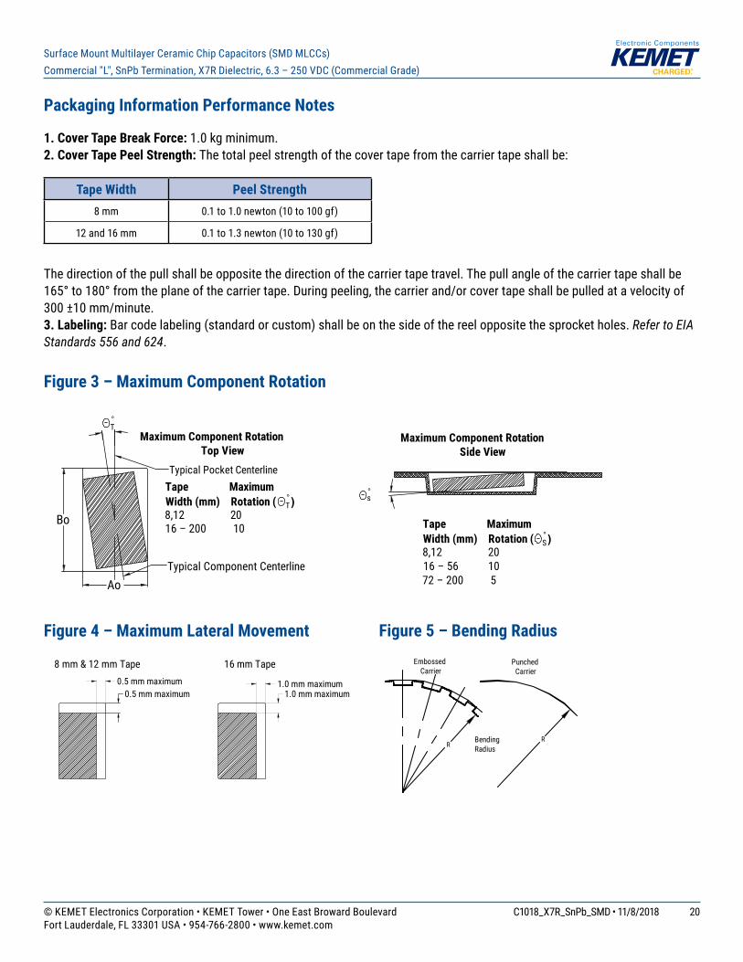
Figure 3 – Maximum Component Rotation
Ao
Bo
°T
°s
Maximum Component RotationTop View
Maximum Component RotationSide View
Tape MaximumWidth (mm) Rotation ( °
T)8,12 20 16 – 200 10 Tape Maximum
Width (mm) Rotation ( °S)
8,12 20 16 – 56 1072 – 200 5
Typical Pocket Centerline
Typical Component Centerline
Figure 4 – Maximum Lateral Movement
0.5 mm maximum0.5 mm maximum
8 mm & 12 mm Tape
1.0 mm maximum1.0 mm maximum
16 mm Tape
Figure 5 – Bending Radius
RRBending
Radius
EmbossedCarrier
PunchedCarrier
21© KEMET Electronics Corporation • KEMET Tower • One East Broward Boulevard C1018_X7R_SnPb_SMD • 11/8/2018Fort Lauderdale, FL 33301 USA • 954-766-2800 • www.kemet.com
Surface Mount Multilayer Ceramic Chip Capacitors (SMD MLCCs)Commercial "L", SnPb Termination, X7R Dielectric, 6.3 – 250 VDC (Commercial Grade)
Figure 6 – Reel Dimensions
A D (See Note)
Full Radius,See Note
B (see Note)
Access Hole atSlot Location(Ø 40 mm minimum)
If present,tape slot in corefor tape start:2.5 mm minimum width x10.0 mm minimum depth
W3 (Includes flange distortion at outer edge)
W2 (Measured at hub)
W1 (Measured at hub)
C(Arbor holediameter)
Note: Drive spokes optional; if used, dimensions B and D shall apply.
N
Table 8 – Reel DimensionsMetricwillgovern
Constant Dimensions — Millimeters (Inches) Tape Size A B Minimum C D Minimum
8 mm 178±0.20(7.008±0.008)
or330±0.20
(13.000±0.008)
1.5 (0.059)
13.0+0.5/−0.2(0.521+0.02/−0.008)
20.2 (0.795)12 mm
16 mm
Variable Dimensions — Millimeters (Inches) Tape Size N Minimum W1 W2 Maximum W3
8 mm
50 (1.969)
8.4+1.5/−0.0(0.331+0.059/−0.0)
14.4 (0.567)
Shallaccommodatetapewidthwithoutinterference12 mm 12.4+2.0/−0.0
(0.488+0.078/−0.0)18.4
(0.724)
16 mm 16.4+2.0/−0.0(0.646+0.078/−0.0)
22.4 (0.882)
22© KEMET Electronics Corporation • KEMET Tower • One East Broward Boulevard C1018_X7R_SnPb_SMD • 11/8/2018Fort Lauderdale, FL 33301 USA • 954-766-2800 • www.kemet.com
Surface Mount Multilayer Ceramic Chip Capacitors (SMD MLCCs)Commercial "L", SnPb Termination, X7R Dielectric, 6.3 – 250 VDC (Commercial Grade)
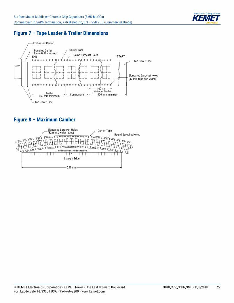
Figure 7 – Tape Leader & Trailer Dimensions
Trailer160 mm minimum
Carrier Tape
END STARTRound Sprocket Holes
Elongated Sprocket Holes(32 mm tape and wider)
Top Cover Tape
Top Cover Tape
Punched Carrier8 mm & 12 mm only
Embossed Carrier
Components
100 mm minimum leader
400 mm minimum
Figure 8 – Maximum Camber
Carrier TapeRound Sprocket Holes
1 mm maximum, either direction
Straight Edge
250 mm
Elongated Sprocket Holes(32 mm & wider tapes)
23© KEMET Electronics Corporation • KEMET Tower • One East Broward Boulevard C1018_X7R_SnPb_SMD • 11/8/2018Fort Lauderdale, FL 33301 USA • 954-766-2800 • www.kemet.com
Surface Mount Multilayer Ceramic Chip Capacitors (SMD MLCCs)Commercial "L", SnPb Termination, X7R Dielectric, 6.3 – 250 VDC (Commercial Grade)
KEMET Electronics Corporation Sales Offi ces
Foracompletelistofourglobalsalesoffices,pleasevisitwww.kemet.com/sales.
DisclaimerAllproductspecifications,statements,informationanddata(collectively,the“Information”)inthisdatasheetaresubjecttochange.ThecustomerisresponsibleforcheckingandverifyingtheextenttowhichtheInformationcontainedinthispublicationisapplicabletoanorderatthetimetheorderisplaced.AllInformationgivenhereinisbelievedtobeaccurateandreliable,butitispresentedwithoutguarantee,warranty,orresponsibilityofanykind,expressedorimplied.
StatementsofsuitabilityforcertainapplicationsarebasedonKEMETElectronicsCorporation’s(“KEMET”)knowledgeoftypicaloperatingconditionsforsuchapplications,butarenotintendedtoconstitute–andKEMETspecificallydisclaims–anywarrantyconcerningsuitabilityforaspecificcustomerapplicationoruse.TheInformationisintendedforuseonlybycustomerswhohavetherequisiteexperienceandcapabilitytodeterminethecorrectproductsfortheirapplication.AnytechnicaladviceinferredfromthisInformationorotherwiseprovidedbyKEMETwithreferencetotheuseofKEMET’sproductsisgivengratis,andKEMETassumesnoobligationorliabilityfortheadvicegivenorresultsobtained.
AlthoughKEMETdesignsandmanufacturesitsproductstothemoststringentqualityandsafetystandards,giventhecurrentstateoftheart,isolatedcomponentfailuresmaystilloccur.Accordingly,customerapplicationswhichrequireahighdegreeofreliabilityorsafetyshouldemploysuitabledesignsorothersafeguards(suchasinstallationofprotectivecircuitryorredundancies)inordertoensurethatthefailureofanelectricalcomponentdoesnotresultinariskofpersonalinjuryorpropertydamage.
Althoughallproduct–relatedwarnings,cautionsandnotesmustbeobserved,thecustomershouldnotassumethatallsafetymeasuresareindictedorthatothermeasures may not be required.
KEMET is a registered trademark of KEMET Electronics Corporation.