Embed Size (px)
Citation preview

Surface Plasmon Interferometer Based on Wedge Metal Waveguide and Its Sensing ApplicationsVolume 4, Number 1, February 2012
Yang MingZi-jian WuHao WuFei XuYan-qing Lu, Senior Member, IEEE
DOI: 10.1109/JPHOT.2012.21865621943-0655/$31.00 ©2012 IEEE

Surface Plasmon Interferometer Basedon Wedge Metal Waveguide and Its
Sensing ApplicationsYang Ming, Zi-jian Wu, Hao Wu, Fei Xu, and
Yan-qing Lu, Senior Member, IEEE
College of Engineering and Applied Sciences and National Laboratory of Solid State Microstructures,Nanjing University, Nanjing 210093, China
DOI: 10.1109/JPHOT.2012.21865621943-0655/$31.00 �2012 IEEE
Manuscript received December 28, 2011; revised January 23, 2012; accepted January 25, 2012. Dateof current version February 17, 2012. This work was supported by 973 programs under Contract2010CB327803, Contract 2011CBA00200, and Contract 2012CB921803, the National Science Founda-tion of China under Programs 11074117 and 60977039, the Priority Academic Program Development ofJiangsu Higher Education Institutions, and Fundamental Research Funds for the Central Universities.Corresponding author: Y. Lu (e-mail: [email protected]).
Abstract:Wepropose a surface plasmon interferometer based on awedgemetal waveguide.Working principles of the device are introduced through theoretical analyses. The interferenceperformances are investigated by finite-difference time-domain (FDTD) method. Because ofthe special wedge geometry, the interferometer shows an extremely low coupling loss incomparison with the previous reports. An interesting surface plasmon polariton (SPP)coupling and splitting phenomenon is found at the wedge section. It is then split into twosurface plasmonmodes in two interference arms. Refractive index sensing applications of thisinterferometer are also discussed, which shows sensitivity as high as 6� 103 nm/RIU.
Index Terms: Sensors, plasmonics.
1. IntroductionSurface plasmon polariton (SPP) is a transverse-magnetic surface electromagnetic excitationpropagating at the interface of a metal and a dielectric [1]. To date, various SPP excitation schemeshavebeendemonstrated, includingprismcoupling [2], grating coupling [3], optical waveguide based [4],enhanced transmission through nanohole arrays [5], and resonance of nanoparticles [6]. Utilizing theunique characteristics of SPP, people have proposed and demonstrated many applications in sensing[2]–[6], spectroscopy [7], and nonlinear optics [8], [9]. Up to date, different kinds of surface plasmonresonance (SPR) sensors have been successfully commercialized. Owing to the unique capability ofSPP to confine the electromagnetic field in the perpendicular direction, SPR sensors could principallybe fabricated in an extremely small size and with high sensitivity. Recently, a new type of SPPinterference sensor was proposed and has attracted plenty of attention [10]–[15]. Ametal film section isdeposited on or partly buried in a dielectric waveguide; therefore, the excited SPPmodes at the top andbottom of the metal film thus may interfere with each other for sensing or modulation applications [10].However, because of the impedancemismatch, the waveguidemode to SPP coupling normally suffersa high loss, at least for one of the SPP modes.
In this paper, we proposed a plasmonic Mach–Zehnder interferometer that consists of a wedgemetal waveguide on a silica substrate. Because of the gradient transition from the waveguide modeto the Bcoupled SPP[ mode, the light to SPP coupling thus exhibits a very low loss. The mode
Vol. 4, No. 1, February 2012 Page 291
IEEE Photonics Journal Surface Plasmon Interferometer
coupling, splitting, and interference characteristics are investigated theoretically by using FDTDanalysis. Applications of our SPP interferometer for refractive index sensing are also studiedshowing a sensitivity of 6� 103 nm/RIU. Our whole paper contains four parts. The basic theory partis introduced in Section 2, including the working principle, the characterizations, and advantages ofour proposal. In Section 3, the sensing application of the SPP interferometer is discussed based onnumerical simulations. Structural parameters are optimized to improve the sensitivity of our sensor.Finally, conclusions are given in Section 4.
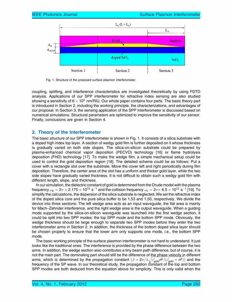
2. Theory of the InterferometerThe basic structure of our SPP interferometer is shown in Fig. 1. It consists of a silica substrate witha doped high index top layer. A section of wedgy gold film is further deposited on it whose thicknessis gradually varied on both side slopes. The silica-on-silicon substrate could be prepared byplasma-enhanced chemical vapor deposition (PECVD) technology [16] or flame hydrolysisdeposition (FHD) technology [17]. To make the wedge film, a simple mechanical setup could beused to control the gold deposition region [18]. The detailed scheme could be as follows: Put acover with a rectangle slot over the substrate. Move the cover left and right periodically during filmdeposition. Therefore, the center area of the slot has a uniform and thicker gold layer, while the twoside slopes have gradually varied thickness. It is not difficult to obtain such a wedgy gold film withdifferent length, slope, and thickness.
In our simulation, the dielectric constant of gold is determined from theDrudemodel with the plasmafrequency !p ¼ 2�� 2:175� 1015 s�1 and the collision frequency !c ¼ 2�� 6:5� 1012 s�1 [19]. Tosimplify the calculations, the dispersion of the silica substrate is neglected.We set the refractive indexof the doped silica core and the pure silica buffer to be 1.53 and 1.50, respectively. We divide thedevice into three sections: The left wedge area acts as an input waveguide, the flat area is mainlyfor Mach–Zehnder interference, and the right wedge area is the output waveguide. When a guidingmode supported by the silica-on-silicon waveguide was launched into the first wedge section, itcould be split into two SPP modes: the top SPP mode and the bottom SPP mode. Obviously, thewedge thickness should be large enough to separate two SPP modes before they enter the twointerferometer arms in Section 2. In addition, the thickness of the bottom doped silica layer shouldbe chosen properly to ensure that the lower arm only supports one mode, i.e., the bottom SPPmode.
The basic working principle of the surface plasmon interferometer is not hard to understand. It justlooks like the traditional ones. The interference is provided by the phase difference between the twoarms. In addition, the wedge section also contributes a tiny beam path difference, but of course, it isnot the main part. The dominating part should still be the difference of the phase velocity in differentarms, which is determined by the propagation constant ð� ¼ 2�=�
ffiffiffiffiffiffiffiffiffiffiffiffiffiffiffiffiffiffiffiffiffiffiffiffiffiffiffiffiffiffiffiffiffiffiffiffiffiffiffiffi"0goldn
2=ð"0gold þ n2Þq
Þ and thefrequency of the SP wave. In our theoretical study, the propagation constant of the top and bottomSPP modes are both deduced from the equation above for simplicity. This is only valid when the
Fig. 1. Structure of the proposed surface plasmon interferometer.
IEEE Photonics Journal Surface Plasmon Interferometer
Vol. 4, No. 1, February 2012 Page 292

thickness of the doped silica layer is large enough. Otherwise, the bottom SPP mode may give aninaccurate result. A more general three layer waveguide model should be used instead [20]. For afixed wavelength, the refractive index difference of the substrate and the environment dominatesthe propagation constants of the top mode and the bottom mode. When they couple back into theoutput waveguide, relative phase difference of the two modes results in interference and asinusoidal spectrum [11]
I ¼ jE j2 ¼ I1 þ I2 þ 2ffiffiffiffiffiffiffiI1I2
pcos
2�L�
ffiffiffiffiffiffiffiffiffiffiffiffiffiffiffiffiffiffiffiffiffiffiffi"0goldn
2env
"0gold þ n2env
s�
ffiffiffiffiffiffiffiffiffiffiffiffiffiffiffiffiffiffiffiffiffiffiffi"0goldn
2bas
"0gold þ n2bas
vuut0@
1A
24 (1)
where "0gold stands for the real part of dielectric constant of gold, and nenv and nbas are theenvironmental index and the refractive index of bottom doped silica layer, respectively. L is the totalinterference length. When phase difference of the top mode and the bottom mode is 0 or �, they willinterfere constructively or destructively to provide the maximum or minimum of the intensity,respectively. To improve the visibility of the interferometer, we should regulate the structural
Fig. 2. (a) Simulated spectrum of an SPP interferometer. (b) Power ratio of top SP mode and bottom SPlaunched into Section 2.
IEEE Photonics Journal Surface Plasmon Interferometer
Vol. 4, No. 1, February 2012 Page 293

parameters of the device to make the minimum be as close to zero as possible. The governingfunctions are as follows [14], [15]:
2ð�b0 � �t0Þ � Reð�b � �t ÞL ¼ ð2m þ 1Þ� (2)
Tb
Tt
��������2
¼ Ab
At
��������2
exp �Imð�b � �t ÞL½ � (3)
where �b0 and �t0 are the phase differences introduced by the coupling processes. Tb and Tt standfor transmission amplitude of the top SPP mode and the bottom SPP mode coupled into the outputsilica-on-silicon waveguide, while Ab and At represent the initial field amplitudes of the top andbottom SPP modes, respectively. �b and �t are the respective propagation constants of the twoSPP modes and they have negative imaginary parts related to their large propagation loss.
In practice, there are three structural parameters that we need to take into account: the totallength of three sections ðL0Þ, the thickness of the doped silica layer ðddopedÞ, and the gradient of thewedge section ðgmðdm; Lw ÞÞ, which is defined as the ratio of the gold film thickness in Section 2 ðdmÞand the length of Section 1 ðLwÞ. In our simulation, we assume L0 ¼ 100 �m, ddoped ¼ 1 �m, and
Fig. 3. (a) Propagation constant varies with the thickness of gold layer. When the thickness increases to37.23 nm, the Bcoupled-SPP[ mode splits into two modes. (b) Splitting process of the mode, the Aulayer thickness of a, b, and c positions are 11 nm, 18 nm, and 39 nm, respectively.
IEEE Photonics Journal Surface Plasmon Interferometer
Vol. 4, No. 1, February 2012 Page 294

gm ¼ 0:015 ðdm ¼ 150 nm; Lw ¼ 10 �mÞ. The interference is shown in Fig. 2(a), while Fig. 2(b)reflects the power ratio between the top and bottom SPP modes. The input TM mode light power isredistributed into two SPP modes, exhibiting a clear mode splitting effect. As is shown in the picture,the proportion of the power launched into top SPP mode decreases with gm. Owing to this effect, aproper splitting ratio could be obtained easily by tuning the structural parameters.
In the interference process, when the input guiding mode is launched into the wedge metalwaveguide, it could excite a metastable Bcoupled SPP[ mode. This mode behaves like a long-rangesurface plasmonmode. However, because of the largemismatch of two sides’ refractive index, it couldnot propagate stably and is split into two independent SPPmodes quickly, i.e., the top and the bottomSPPmodes. An analytic three layer waveguidemodel [20] is used to study the generation and splittingof this coupledmodeas shown in Fig. 3.When the gold layer is thinner than 37.23 nm, there is only onemodewith light field on both sides of the film. Fig. 3(b) shows the splitting process of themode, positionBa[ corresponds to the position where the thickness of Au layer is 11 nm, and the field has hardly split.The thickness of Au layer of position Bb[ is 18 nm, and the splitting has happened. Position Bc[corresponds to a total splitting of themodewith a thickness of 39 nm. If the gold film thickness is largerthan 39 nm, the top and bottom SPPmodes are more separated with different propagation constants.As a consequence, the interference length L does not just mean the total length of three sections. It isthe length of the total effective interference path after the Bcoupled SPP[mode is split and before thesplit top and bottommodes are recombined in Section 3. However, because the Bcoupled SPP[modeis just a transition state with only nanometer scale propagation length, L is almost equal to the totallength of three sections (L0), as shown in Fig. 1.
Owing to the Bcoupled SPP[ mode, the total interference process is a continuously varyingprocess, and therefore, losses arisen from uncontinuity of the structure could be avoided. Couplingloss of the interferometer which is defined by the ratio of total power of two SPP modes, and theinput power is shown in Fig. 4. Corresponding to gm ¼ 0:0125, the coupling loss is about 2 dB. Asgm gets larger, the loss becomes lower. It even reduces to below 1 dB when gm increases to0.0175. It is worth noticing that the propagation attenuation caused by the imagined part of thepropagation constant is included, and therefore, the coupling loss of smaller gm which has a longercoupling section is larger. To have a clearer physical image, we remove this portion by follow-uptheoretical treatment. It could be seen that the loss is even smaller. Overall, the total coupling loss ismuch lower compared with previous reports [10].
Fig. 4. Total coupling loss of the interferometer to the top and bottom SPP mode as a function of thegradient of wedge section.
IEEE Photonics Journal Surface Plasmon Interferometer
Vol. 4, No. 1, February 2012 Page 295

3. Sensing ApplicationsThe surface plasmon interferometer proposed above has many applications. As an example, wewould study its refractive index sensing properties. The top interference path and the bottominterference path are treated as the sensing arm and the reference arm, respectively. When theenvironmental refractive index changes, the propagation constant of the top SPP mode variesaccordingly. However, the propagation constant of the bottom SPP mode is insensitive, andtherefore, the relative phase difference of the two modes is the function of environment refractiveindex. This effect drives the device to be sensitive to variation of environment index, andcorrespondingly, the transmission spectrum of the device will present a shift. The shift of valleys inthe spectrum is usually used for sensing. Furthermore, in a practical device, the analyte shouldcover at least the total interference length L, and because of the field penetration outside the goldfilm, the analyte’s thickness should be large enough to take all top SPP field. From our simulation,a 9 2 �m-thick analyte is suitable with almost all fields included. Otherwise, an analyte that is too thinmay result in a lower sensitivity.
Simulations of our device are carried out by the commercial software Rsoft CAD-Layout throughthe finite-difference time-domain (FDTD) method. We use the 2-D model in our simulations, andthe numerical parameters of spatial meshes are 0.03 �m in the transverse direction and 0.1 �m in thepropagation direction, respectively. In our calculations, the three structural parameters of the
Fig. 5. (a) Transmission of the surface plasmon interferometer sensor as a function of refractive index.The working wavelength is fixed at 1.4 �m. (b) Transmission of the surface plasmon interferometersensor as a function of wavelength. The refractive index of the water sample is set to be 1.33.
IEEE Photonics Journal Surface Plasmon Interferometer
Vol. 4, No. 1, February 2012 Page 296

interferometer sensor mentioned above should be optimized to for better sensing performances.Among these parameters, influence of the total length L is expressed directly in (2) and (3). It plays amore important role because the peak positions of the transmission spectrum of the device aredetermined mainly by it. Besides, another parameter of the sensor, i.e., the FSR is the function ofL ðFSR � �2=�neffLÞ. As L becomes larger, the FSR will be shorter with a sharper transmissionvalley. The full-width at half-maximum (FWHM) power thus will be reduced, and the Q-factorðQ ¼ �=FWHMÞ of the sensor will be improved. In addition, ddoped affects Tb and Tt at the same time,while smaller gm results in a larger Tt . The ratio jTb=Tt j2 thus could be tuned accurately by adjustingthese two parameters, together with the total length L. An index sensor with optimized performancesthus could be obtained according to different application requirements.
Fig. 5 shows the performance of an SPP interferometer with L0 ¼ 114:6 �m for the total length,ddoped ¼ 1:15 �m for the waveguide layer thickness, and gm ¼ 0:012 ðdm ¼ 150 nm; Lw ¼12:15 �mÞ for the wedge gradient, respectively. The transmission which is defined by (1) is plottedas a function of refractive index and wavelength in Fig. 5(a) and (b), respectively. In Fig. 5(a), thewavelength is fixed at 1.4 �m; and in Fig. 5(b), the environmental refractive index of the sample isset at 1.33, i.e., the index of water.
Fig. 5(a) displays the interference characteristics of the sensor. Relative phase of the top andbottom modes varies rapidly with the refractive index. According to Fig. 5(a), the resonance periodis �0.012, i.e., a 2� phase difference can be brought by a tiny variation of refractive index. Fig. 5(b)shows the wavelength response of the sensor. We can see that for our device, FSR is �78 nm, andFWHM is �21 nm. Combining two types of properties to estimate, the high sensitivity of our devicecould be predicted.
Fig. 6. (a) Transmission spectra for refractive index 1.326, 1.328, 1.330, and 1.332 of the sample.(b) Transmission minimum as a function of environmental refractive index.
IEEE Photonics Journal Surface Plasmon Interferometer
Vol. 4, No. 1, February 2012 Page 297

For sensing applications, the regime which is called Bwavelength interrogation mode[ [10] isusually more useful. We calculate the transmission spectrums for refractive index of 1.326, 1.328,1.330, and 1.332, and the data are collected together and shown in Fig. 6(a). Further calculationsare also made to obtain sensitivity of our device. Fig. 6(b) shows the position of the resonancewavelength which corresponds to transmission minimum as a function of sample refractive index.
From Fig. 6(b), we could see that wavelength at transmission minimum reduces linearly againstsample refractive index improving. The sensitivity of the device is around 6:0� 103 nm/RIU. Thissensitivity could also be estimated by theoretical analyses. As mentioned above, the analyticexpression of the bottom SPP mode is also used in the derivation here. Controlling equations aregiven as follows [11], [13]:
S ¼ ��
�n¼ �
n3top
ffiffiffiffiffiffiffiffiffiffiffiffiffiffiffiffiffiffiffiffiffiffiffi"0goldn
2top
"0gold þ n2top
vuut0@
1A
3=2 ffiffiffiffiffiffiffiffiffiffiffiffiffiffiffiffiffiffiffiffiffiffiffi"0goldn
2top
"0gold þ n2top
vuut �
ffiffiffiffiffiffiffiffiffiffiffiffiffiffiffiffiffiffiffiffiffiffiffi"0goldn
2bot
"0gold þ n2bot
vuut24
35:
,(4)
Assuming � ¼ 1:40 �m, the sensitivity is calculated to be 6:9� 103 nm/RIU, and the difference isintroduced in by the approximations used to derivate the expression of sensitivity and the errorbrought by the numerical method itself.
In both direct data fitting or theoretical analysis, our sensor show a much higher sensitivity thansome previous reported results. However, this is mainly because of the different material system, andtherefore, the direct comparison is difficult. We use a doped Silica waveguide while a Silicon-on-insulator substrate was normally employed before [10]. Both of these two approaches haveadvantages and disadvantages. For example, our sensor shows a long device length (over 100 �m),but amore compact�10 �mSPP sensor was reported in [10]. Therefore, our sensor requires a largeramount of analyte. This is one drawback of the present sensor. However, the longer device results infiner spectrumwith shorter FSR/FWHM. So, the L value should be well selected according to differentapplications. Although we set a long L, it also could be smaller if a sensor with lower loss and largersensing range is desired [21]. In addition, because L affects both the top and bottom SPP’sattenuation while they are not identical, L is also a tuning factor to adjust the contrast of spectrumpeaks and valleys according to (2) and (3). For our sensor, the spectrum contrast reaches around20 dB, which is quite good.
4. ConclusionWe have presented in this paper a surface plasmon interferometer based on wedge metalwaveguide. Working principles of this device are discussed through theoretical analyses. This isattributed to the special mode supported by the wedge metal waveguide, i.e., the Bcoupled SPP[mode. The total coupling loss of the interferometer is very low. Its applications for refractive indexsensing are also investigated. Owing to characteristics of surface plasmon, the sensor has a reallyhigh sensitivity. The size of the device could be controlled as small as a micrometer order ofmagnitude, which makes it a promising candidate for nanophotonic integration.
References[1] H. Raether, Surface Plasmons on Smooth and Rough Surfaces and on Gratings. Berlin, Germany: Springer-Verlag,
1988.[2] G. G. Nenninger, P. Tobiska, J. Homola, and S. S. Yee, BLong-range surface plasmons for high-resolution surface
plasmon resonance sensors,[ Sens. Actuators B, Chem., vol. 74, no. 1, pp. 145–151, Apr. 2001.[3] S. Y. Wu, H. P. Ho, W. C. Law, C. Lin, and S. K. Kong, BHighly sensitive differential phase-sensitive surface plasmon
resonance biosensor based on the Mach–Zehnder configuration,[ Opt. Lett., vol. 29, no. 20, pp. 2378–2380, Oct. 2004.[4] J. Shibayama, BThree-dimensional numerical investigation of an improved surface plasmon resonance waveguide
sensor,[ IEEE Photon. Technol. Lett., vol. 22, no. 9, pp. 643–645, May 2010.[5] A. G. Brolo, R. Gordon, B. Leathem, and K. L. Kavanagh, BSurface plasmon sensor based on the enhanced light
transmission through arrays of nanoholes in gold films,[ Langmuir, vol. 20, no. 12, pp. 4813–4815, May 2004.[6] J. J. Mock, D. R. Smith, and S. Schultz, BLocal refractive index dependence of plasmon resonance spectra from
individual nanoparticles,[ Nano Lett., vol. 3, no. 4, pp. 485–491, Mar. 2003.
IEEE Photonics Journal Surface Plasmon Interferometer
Vol. 4, No. 1, February 2012 Page 298

[7] C. Sonnichsen, S. Geier, N. Hecker, G. von Plessen, J. Feldmann, H. Ditlbacher, B. Lamprecht, J. Krenn, F. Aussennegg,V. Chan, J. Spatz, and M. Moller, BSpectroscopy of single metallic nanoparticles using total internal reflectionmicroscopy,[ Appl. Phys. Lett., vol. 77, no. 19, pp. 2949–2951, Nov. 2000.
[8] Z. J. Wu, X. K. Hu, Z. Y. Yu, W. Hu, F. Xu, and Y. Q. Lu, BNonlinear plasmonic frequency conversion throughquasiphase matching,[ Phys. Rev. B, Condens. Matter, vol. 82, no. 15, p. 155 107, Oct. 2010.
[9] F. F. Lu, T. Li, X. P. Hu, Q. Q. Cheng, S. N. Zhu, and Y. Y. Zhu, BEfficient second-harmonic generation in nonlinearplasmonic waveguide,[ Opt. Lett., vol. 36, no. 17, pp. 3371–3373, Sep. 2011.
[10] P. Debackere, S. Scheerlinck, P. Bienstman, and R. Baets, BSurface plasmon interferometer in silicon-on-insulator:Novel concept for an integrated biosensor,[ Opt. Exp., vol. 14, no. 16, pp. 7063–7072, Aug. 2006.
[11] X. Wu, J. Zhang, J. Chen, C. Zhao, and Q. Gong, BRefractive index sensor based on surface-plasmon interference,[Opt. Lett., vol. 34, no. 3, pp. 392–394, Feb. 2009.
[12] P. Debackere, R. Baets, and P. Bienstman, BBulk sensing experiments using a surface-plasmon interferometer,[ Opt.Lett., vol. 34, no. 18, pp. 2858–2860, Sep. 2009.
[13] Q. Q. Gan, Y. K. Gao, and F. J. Bartoli, BVertical plasmonic Mach–Zehnder interferometer for sensitive optical sensing,[Opt. Exp., vol. 17, no. 23, pp. 20 749–20 755, Nov. 2009.
[14] K. Q. Le and P. Bienstman, BEnhanced sensitivity of silicon-on-insulator surface plasmon interferometer with additionalsilicon layer,[ IEEE Photon. J., vol. 3, no. 3, pp. 538–545, Jun. 2011.
[15] M. S. Kwon, BTheoretical investigation of an interferometer-type plasmonic biosensor using a metal-insulator-siliconwaveguide,[ Plasmonics, vol. 5, no. 4, pp. 347–354, Dec. 2010.
[16] H. Ou, BDifferent index contrast silica-on-silicon waveguides by PECVD,[ Electron. Lett., vol. 39, no. 2, pp. 212–213,Jan. 2003.
[17] A. Kilian, J. Kirchhof, B. Kuhlow, G. Przyrembel, and W. Wischmann, BBirefringence free planar optical waveguidemade by flame hydrolysis deposition (FHD) through tailoring of the overcladding,[ J. Lightw. Technol., vol. 18, no. 2,pp. 193–198, Feb. 2000.
[18] M. R. Witzman, R. A. Bradley, C. W. Lantman, and E. R. Cow, BLinear aperture deposition apparatus and coatingprocess,[ U.S. Patent 6 202 591 B1, Mar. 20, 2001.
[19] S. Linden, C. Enkrich, M. Wegener, J. Zhou, T. Koschny, and C. M. Soukoulis, BMagnetic response of metamaterials at100 Terahertz,[ Science, vol. 306, no. 5700, pp. 1351–1353, Nov. 2004.
[20] G. Lifante, Integrated Photonics: Fundamentals. Chichester, U.K.: Wiley, 2003.[21] S. Y. Zhang, Q. Zhong, X. S. Qian, X. W. Lin, F. Xu, W. Hu, and Y. Q. Lu, BA three-beam path photonic crystal fiber
modal interferometer and its sensing applications,[ J. Appl. Phys., vol. 108, no. 2, p. 023107, Jul. 2010.
IEEE Photonics Journal Surface Plasmon Interferometer
Vol. 4, No. 1, February 2012 Page 299