Embed Size (px)
Citation preview

SVT UPGRADE:SVT UPGRADE: Memory CardsMemory Cards DesignsDesigns
Design Team MembersMel Shochet <[email protected]>
Harold Sanders <[email protected]>
Fukun Tang <[email protected]>
Un-Ki Yang <[email protected]>
Ivan Furic <[email protected]>
Jahred Adelman <[email protected]>
Ted Liu <[email protected]>
Takasumi Maruyama <[email protected]>
Paola Giannetti <[email protected]>
Alberto Annovi <[email protected]>
Franco Spinella <[email protected]>
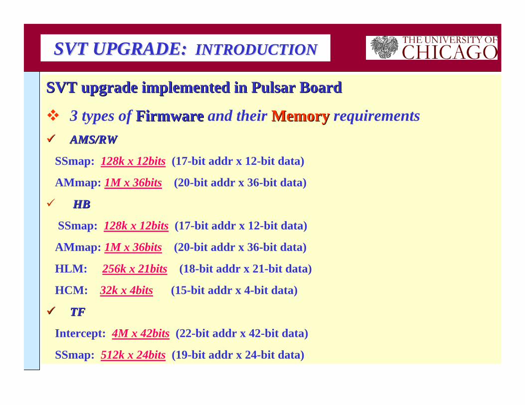
SVT upgrade implemented in Pulsar BoardSVT upgrade implemented in Pulsar Board
3 types of FirmwareFirmware and their MemoryMemory requirementsAMS/RWAMS/RW
SSmap: 128k x 12bits (17-bit addr x 12-bit data)
AMmap: 1M x 36bits (20-bit addr x 36-bit data)
HBHB
SSmap: 128k x 12bits (17-bit addr x 12-bit data)
AMmap: 1M x 36bits (20-bit addr x 36-bit data)
HLM: 256k x 21bits (18-bit addr x 21-bit data)
HCM: 32k x 4bits (15-bit addr x 4-bit data)
TFTF
Intercept: 4M x 42bits (22-bit addr x 42-bit data)
SSmap: 512k x 24bits (19-bit addr x 24-bit data)
SVT UPGRADE:SVT UPGRADE: INTRODUCTIONINTRODUCTION

SVT UPGRADE: SVT UPGRADE: System ConfigurationsSystem Configurations
Mezzanine HB AMS/RW TF
2 types of mezzanine memory cards fit all2 types of mezzanine memory cards fit all(1) M4M: 4M x 48bits memory card
(2) M512K: 512K x 24bits memory card
System Configurations:
M4M
M512
M4M
M512
AMmap/SSmap
HLM
None
None
AMmap
SSmap
None
None
Intercept1
SSmap
Intercept2
SSmap
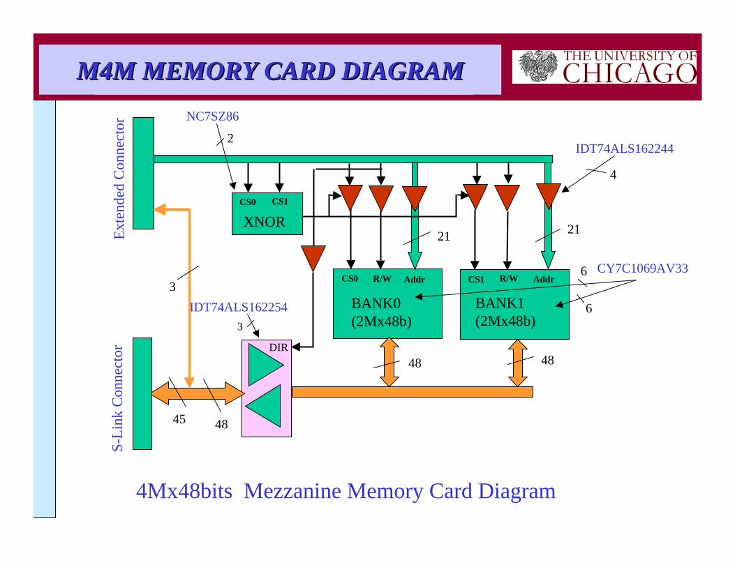
Introduction to TileCal Readout SystemM4M MEMORY CARD DIAGRAMM4M MEMORY CARD DIAGRAM
R/WCS0 Addr R/WCS1 Addr
BANK0 (2Mx48b)
BANK1 (2Mx48b)
XNORCS0 CS1
S-Li
nk C
onne
ctor
Exte
nded
Con
nect
or
3
45 48
48
2121
48
4Mx48bits Mezzanine Memory Card Diagram
IDT74ALS162254
CY7C1069AV33
6
6
3
IDT74ALS162244
NC7SZ86
2
4
DIR

Memory Access SpeedMemory Access Speed
M4M Memory Access SpeedM4M Memory Access Speed
Single word write-then-read or read-then-write: ~40Mhz
T = T(flight_max) + Tpd (addr_buffer) + Tpd(data_buffer)
+ T(fpga_setup) + T(mem_access) + T(skew_margin)
= 3.6ns + 3ns + 3ns + 4ns + 10ns + 2ns = 24.6ns (~40Mhz)
Multiple write or multiple read: ~60Mhz
T= T(mem_access) + T(fpga_setup) + T(skew_margin)
= 10ns + 4ns + 2ns = 16ns (~60Mhz)
Latency: ~25ns

7ns
0ns
16ns
7ns
MEMORY WRITE TIMINGMEMORY WRITE TIMING
Multiple Write TimingMultiple Write Timing
5.5ns
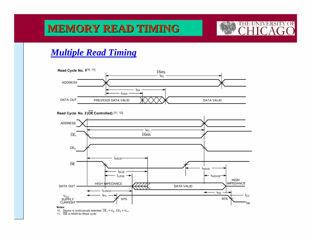
MEMORY READ TIMINGMEMORY READ TIMING
Multiple Read Timing
16ns
16ns
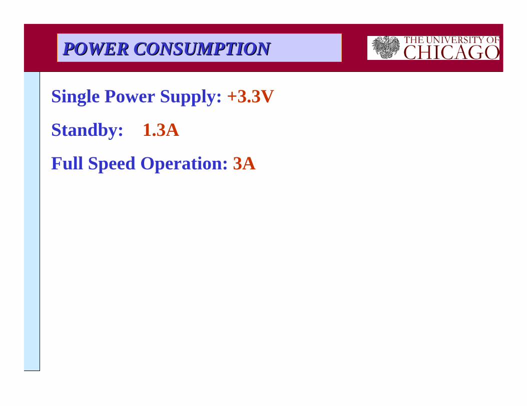
POWER CONSUMPTIONPOWER CONSUMPTION
Single Power Supply: +3.3V
Standby: 1.3A
Full Speed Operation: 3A
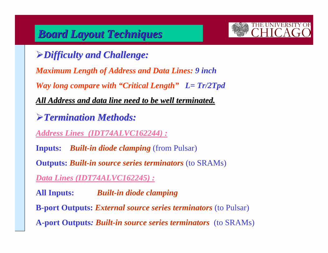
Board Layout TechniquesBoard Layout Techniques
Difficulty and Challenge:Difficulty and Challenge:Maximum Length of Address and Data Lines: 9 inch
Way long compare with “Critical Length” L= Tr/2Tpd
All Address and data line need to be well terminated.All Address and data line need to be well terminated.
Termination Methods:Termination Methods:Address Lines (IDT74ALVC162244) :
Inputs: Built-in diode clamping (from Pulsar)
Outputs: Built-in source series terminators (to SRAMs)
Data Lines (IDT74ALVC162245) :
All Inputs: Built-in diode clamping
B-port Outputs: External source series terminators (to Pulsar)
A-port Outputs: Built-in source series terminators (to SRAMs)
Board Layout TechniquesBoard Layout Techniques
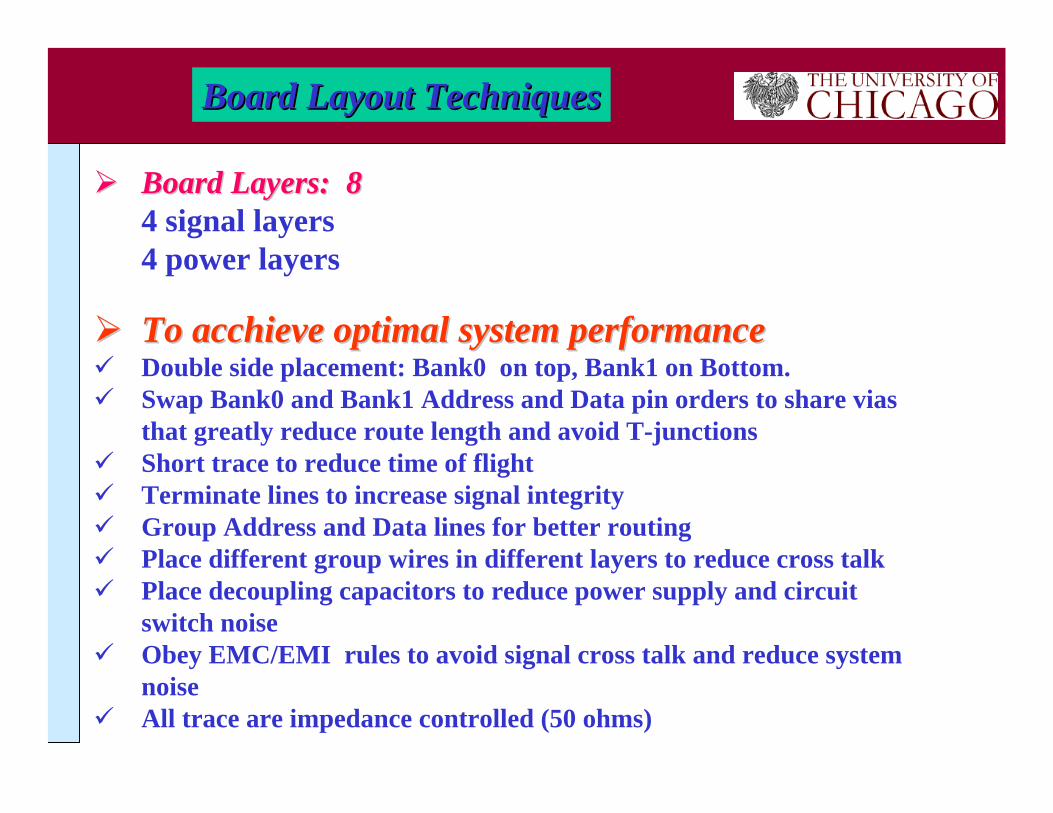
Board Layers: 8Board Layers: 84 signal layers4 power layers
To To acchieveacchieve optimal system performanceoptimal system performanceDouble side placement: Bank0 on top, Bank1 on Bottom.Swap Bank0 and Bank1 Address and Data pin orders to share viasthat greatly reduce route length and avoid T-junctionsShort trace to reduce time of flightTerminate lines to increase signal integrityGroup Address and Data lines for better routing Place different group wires in different layers to reduce cross talkPlace decoupling capacitors to reduce power supply and circuit switch noiseObey EMC/EMI rules to avoid signal cross talk and reduce systemnoiseAll trace are impedance controlled (50 ohms)
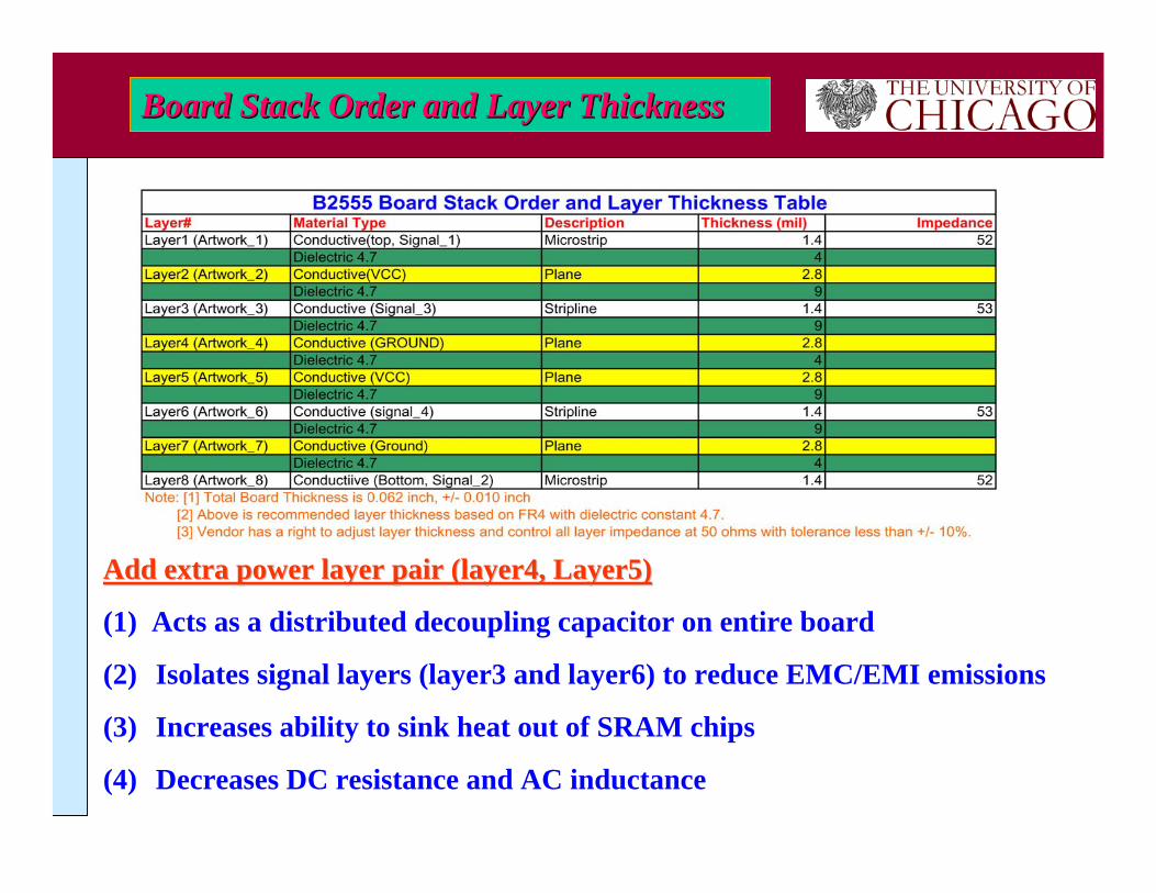
Board Stack Order and Layer ThicknessBoard Stack Order and Layer Thickness
Add extra power layer pair (layer4, Layer5)Add extra power layer pair (layer4, Layer5)
(1) Acts as a distributed decoupling capacitor on entire board
(2) Isolates signal layers (layer3 and layer6) to reduce EMC/EMI emissions
(3) Increases ability to sink heat out of SRAM chips
(4) Decreases DC resistance and AC inductance

M4M Mezzanine Card DimensionsM4M Mezzanine Card Dimensions

M4M ONM4M ON--BOARD LED DISPLAYSBOARD LED DISPLAYS
M4M OnM4M On--Board LED DisplaysBoard LED Displays

Address or Data Waveforms @ Address or Address or Data Waveforms @ Address or Data Buffer Inputs Data Buffer Inputs
Bank0Addr Buffer or Data BufferFPGA Addr Driver on Pulsar 9-inch
Bank1
Input diode clamping

Addr BufferFPGA Addr Driver on Pulsar
SRAM6
SRAM1
Address Signal Waveforms at SRAM InputsAddress Signal Waveforms at SRAM Inputs
Bank09-inch
Addr BufferFPGA Addr Driver on Pulsar
Bank1
Bank0
FPGA Data Driver on Pulsar Data Buffer
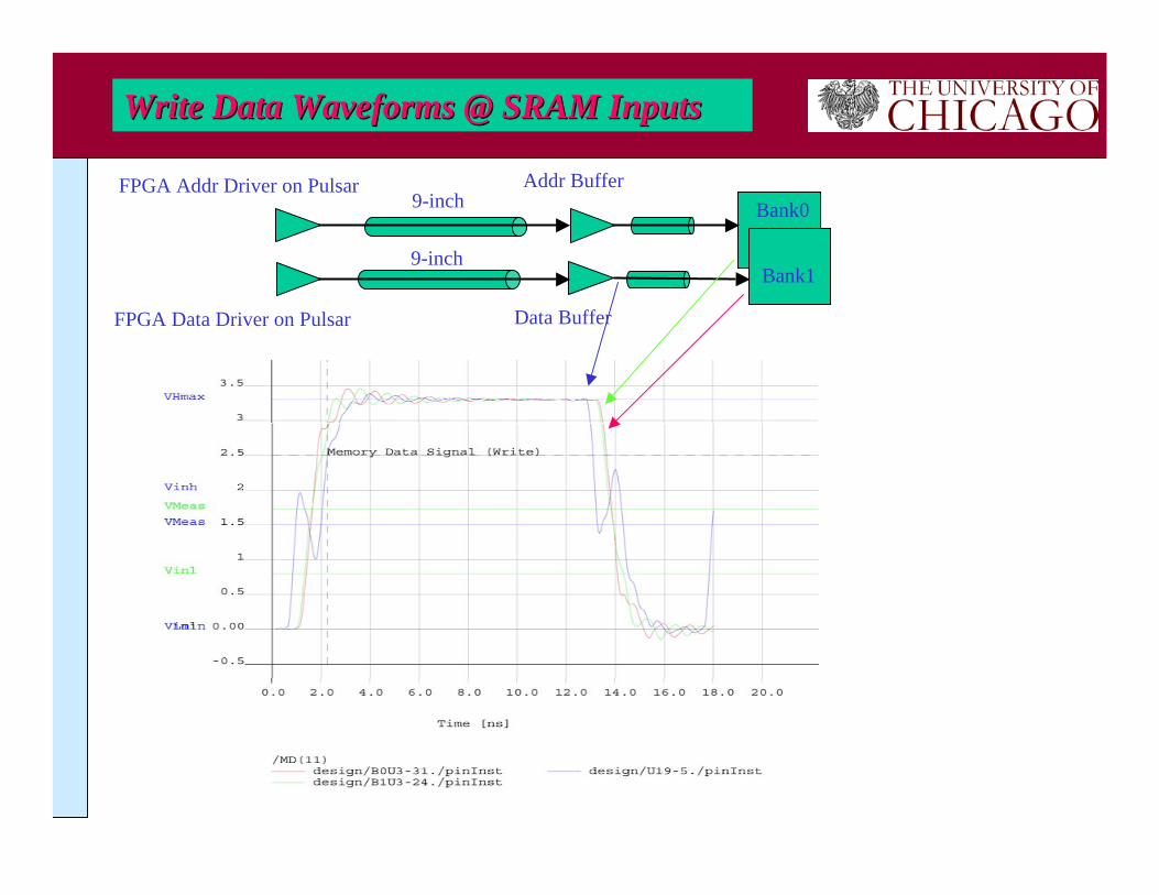
Write Data Waveforms @ SRAM InputsWrite Data Waveforms @ SRAM Inputs
9-inch
9-inch

Bank1
Bank0Addr BufferFPGA Addr Driver on Pulsar
FPGA Data Receiver on Pulsar Data Buffer
Read Data Waveforms @Data Buffer InputsRead Data Waveforms @Data Buffer Inputs
9-inch
9-inch

Bank1
Bank0Addr BufferFPGA Addr Driver on Pulsar
FPGA Data Receiver on Pulsar Data Buffer
7-inch (inner layer)
Read Data Waveforms @ FPGA InputsRead Data Waveforms @ FPGA Inputs
9-inch
M4M Mezzanine Card Design Info WebsiteM4M Mezzanine Card Design Info Website
http://edg.uchicago.edu/~tang/Memory/sram_M4M.html