Embed Size (px)
Citation preview

1
© 2008 Microchip Technology Incorporated. All Rights Reserved. WebSeminar Title Slide 1
Switch Mode Power Supply Topologies
The Buck Converter
Welcome to this Web seminar on Switch Mode Power Supply Topologies. In this webinar, we will analyze the Buck Converter topology. The buck converter converts a higher input voltage to a lower output voltage. A similar function is also performed by a linear regulator. The most important difference then between the linear and switching approach is that the switching approach allows for a much higher efficiency.
2
© 2008 Microchip Technology Incorporated. All Rights Reserved. WebSeminar Title Slide 2
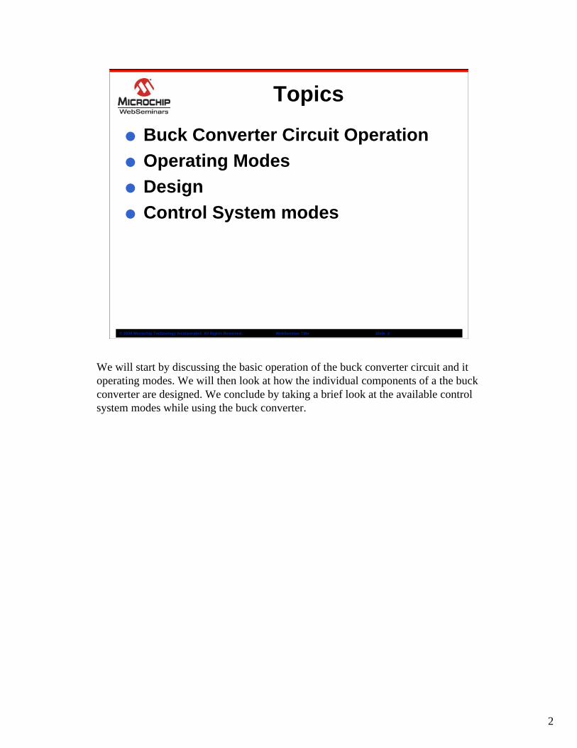
Topics
Buck Converter Circuit OperationOperating ModesDesignControl System modes
We will start by discussing the basic operation of the buck converter circuit and it operating modes. We will then look at how the individual components of a the buck converter are designed. We conclude by taking a brief look at the available control system modes while using the buck converter.
3
© 2008 Microchip Technology Incorporated. All Rights Reserved. WebSeminar Title Slide 3
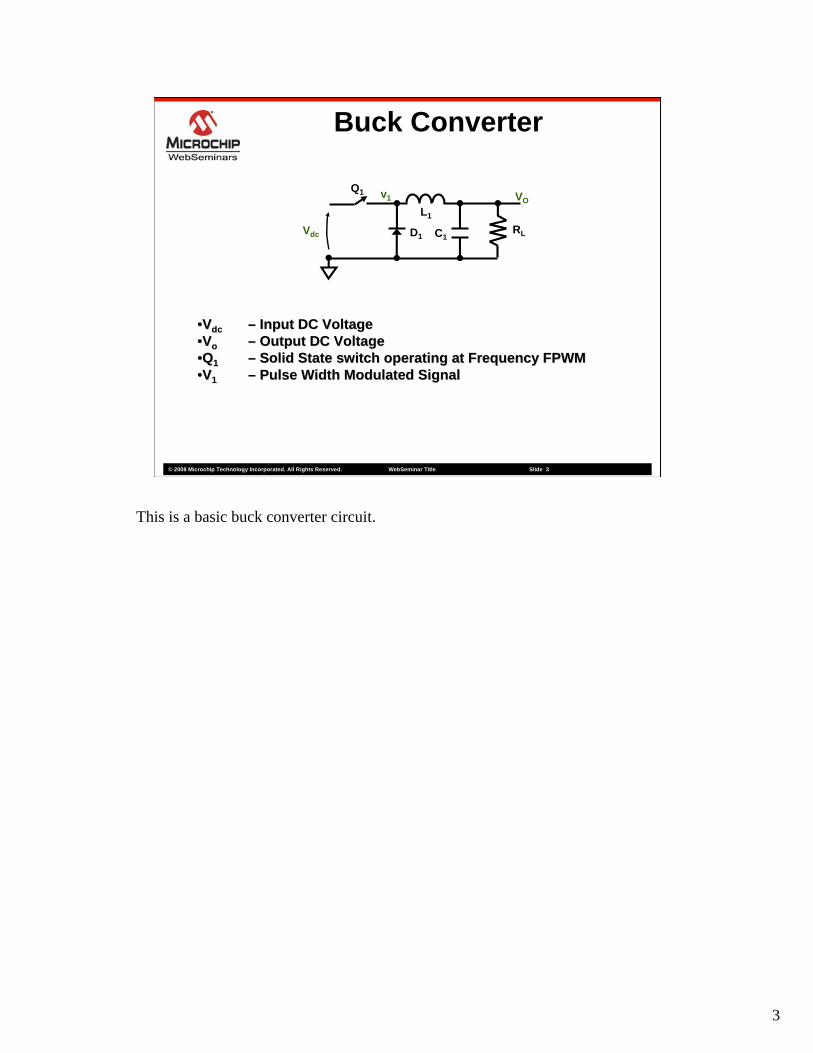
Buck Converter
RL
VO
D1
v1
C1
L1
Vdc
Q1
••VVdcdc –– Input DC VoltageInput DC Voltage••VVoo –– Output DC VoltageOutput DC Voltage••QQ11 –– Solid State switch operating at Frequency FPWMSolid State switch operating at Frequency FPWM••VV11 –– Pulse Width Modulated SignalPulse Width Modulated Signal
This is a basic buck converter circuit.
4
© 2008 Microchip Technology Incorporated. All Rights Reserved. WebSeminar Title Slide 4
Buck Converter
RL
VO
D1
v1
C1
L1
Vdc
Q1
••VVdcdc –– Input DC VoltageInput DC Voltage••VVoo –– Output DC VoltageOutput DC Voltage••QQ11 –– Solid State switch operating at Frequency FPWMSolid State switch operating at Frequency FPWM••VV11 –– Pulse Width Modulated SignalPulse Width Modulated Signal
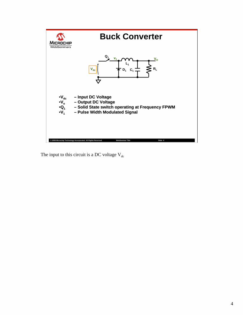
The input to this circuit is a DC voltage Vdc
5
© 2008 Microchip Technology Incorporated. All Rights Reserved. WebSeminar Title Slide 5
Buck Converter
RL
VO
D1
v1
C1
L1
Vdc
Q1
••VVdcdc –– Input DC VoltageInput DC Voltage••VVoo –– Output DC VoltageOutput DC Voltage••QQ11 –– Solid State switch operating at Frequency FPWMSolid State switch operating at Frequency FPWM••VV11 –– Pulse Width Modulated SignalPulse Width Modulated Signal
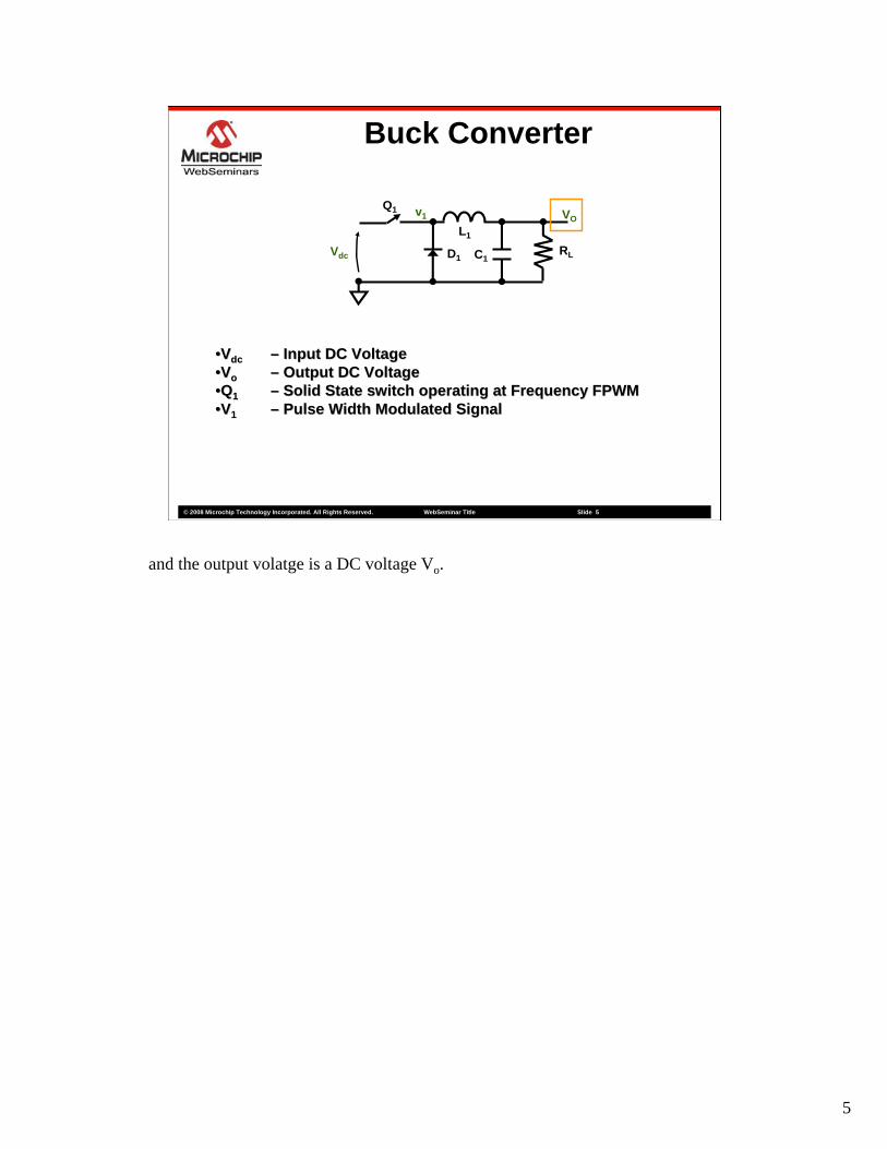
and the output volatge is a DC voltage Vo.
6
© 2008 Microchip Technology Incorporated. All Rights Reserved. WebSeminar Title Slide 6
Buck Converter
RL
VO
D1
v1
C1
L1
Vdc
Q1
••VVdcdc –– Input DC VoltageInput DC Voltage••VVoo –– Output DC VoltageOutput DC Voltage••QQ11 –– Solid State switch operating at Frequency FPWMSolid State switch operating at Frequency FPWM••VV11 –– Pulse Width Modulated SignalPulse Width Modulated Signal
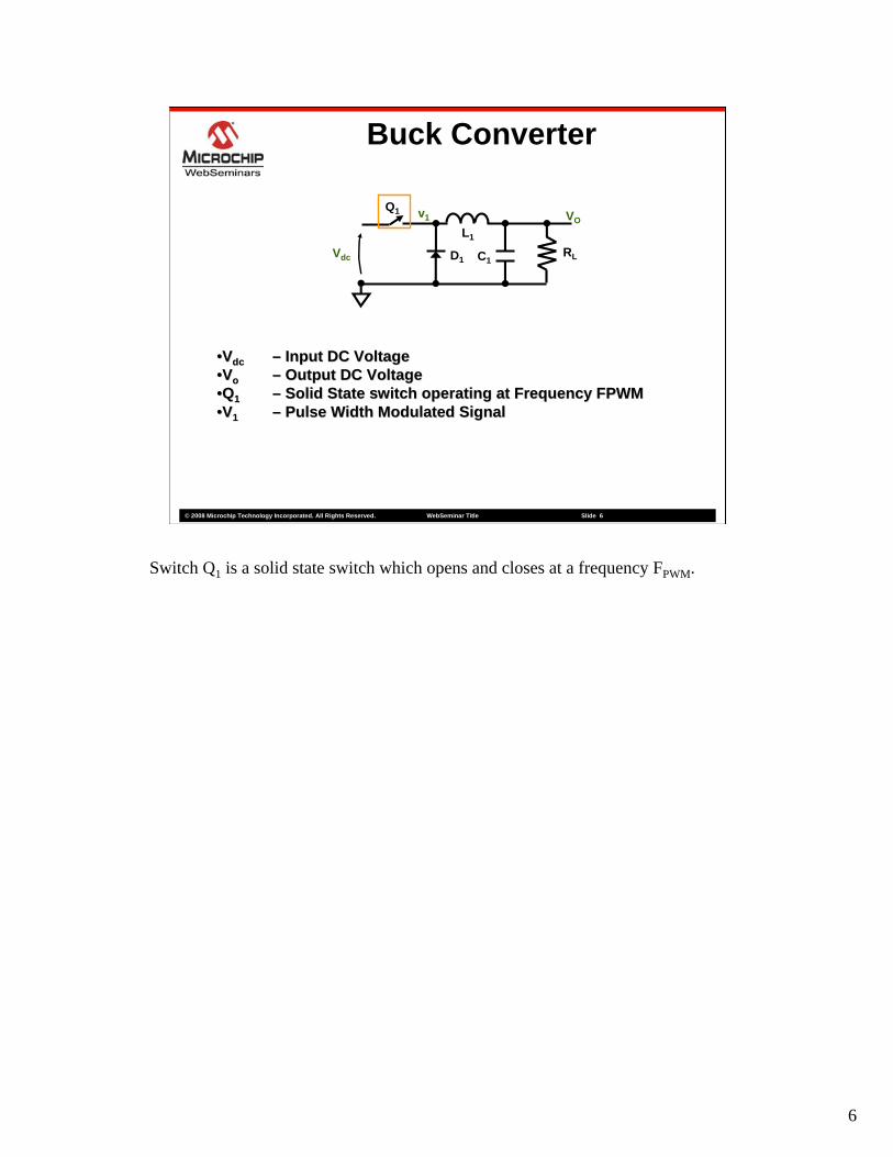
Switch Q1 is a solid state switch which opens and closes at a frequency FPWM.
7
© 2008 Microchip Technology Incorporated. All Rights Reserved. WebSeminar Title Slide 7
Buck Converter
RL
VO
D1
v1
C1
L1
Vdc
Q1
••VVdcdc –– Input DC VoltageInput DC Voltage••VVoo –– Output DC VoltageOutput DC Voltage••QQ11 –– Solid State switch operating at Frequency FPWMSolid State switch operating at Frequency FPWM••VV11 –– Pulse Width Modulated SignalPulse Width Modulated Signal
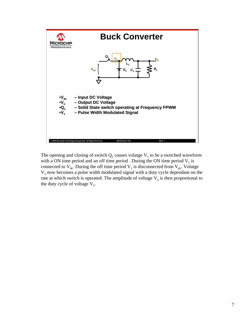
The opening and closing of switch Q1 causes volatge V1 to be a switched waveform with a ON time period and an off time period . During the ON time period V1 is connected to Vdc. During the off time period V1 is disconnected from Vdc. Volatge V1 now becomes a pulse width modulated signal with a duty cycle dependant on the rate at which switch is operated. The amplitude of voltage Vo is then proportional to the duty cycle of voltage V1.
8
© 2008 Microchip Technology Incorporated. All Rights Reserved. WebSeminar Title Slide 8
Buck Converter
RL
VO
D1
v1
C1
L1
Vdc
Q1
RL
VO
D1
v1
C1
L1
V
Q1
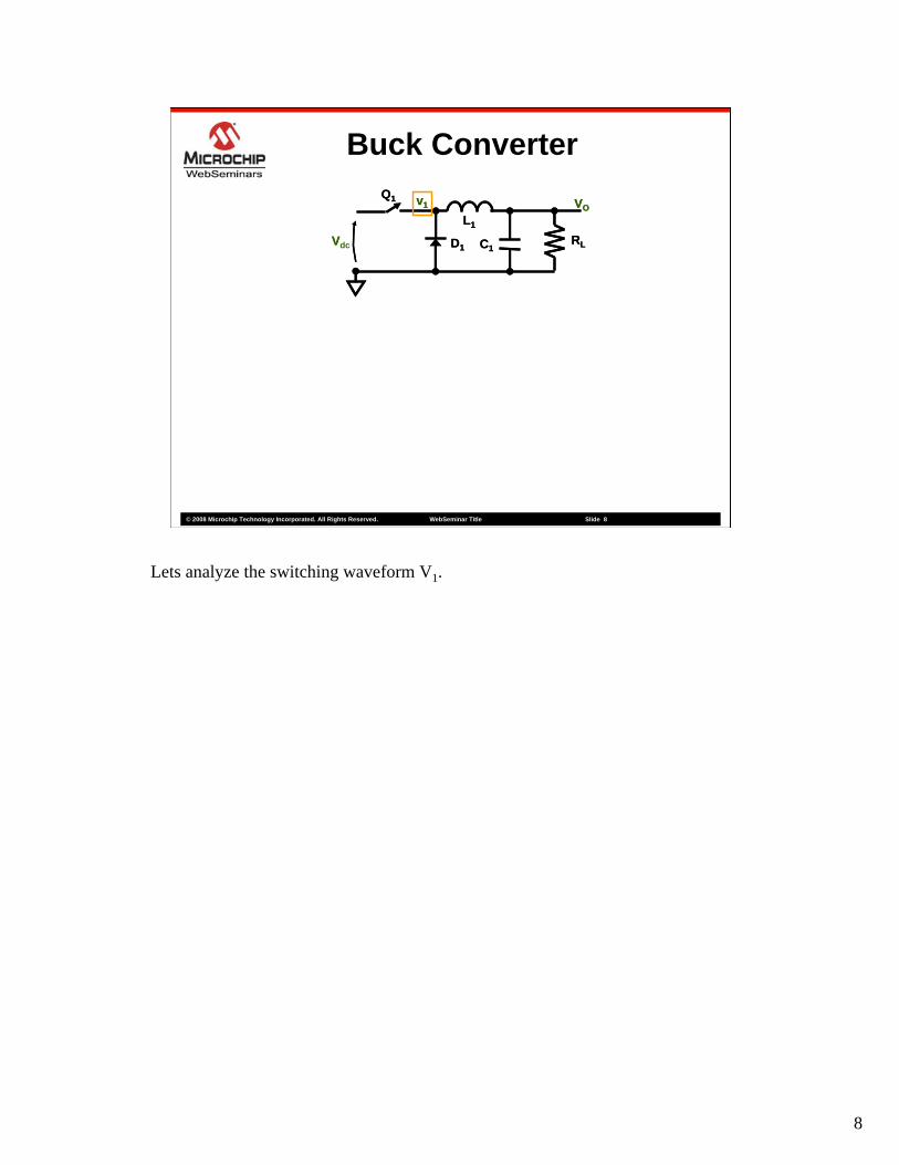
Lets analyze the switching waveform V1.
9
© 2008 Microchip Technology Incorporated. All Rights Reserved. WebSeminar Title Slide 9
Buck Converter
RL
VO
D1
v1
C1
L1
Vdc
Q1
RL
VO
D1
v1
C1
L1
V
Q1
τ
T
t
A
V1(t)
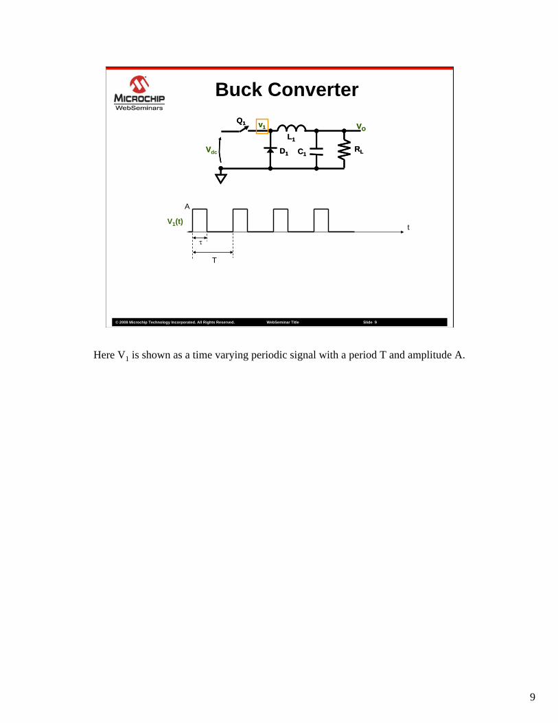
Here V1 is shown as a time varying periodic signal with a period T and amplitude A.
10
© 2008 Microchip Technology Incorporated. All Rights Reserved. WebSeminar Title Slide 10
Buck Converter
RL
VO
D1
v1
C1
L1
Vdc
Q1
RL
VO
D1
v1
C1
L1
V
Q1
τ
T
t
A
V1(t)
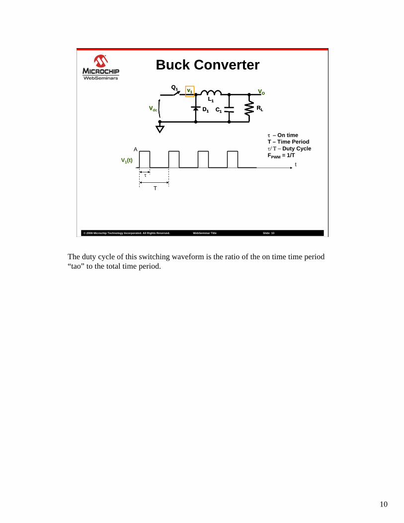
τ − On timeT – Time Periodτ/ Τ − Duty CycleFPWM = 1/T
The duty cycle of this switching waveform is the ratio of the on time time period “tao” to the total time period.
11
© 2008 Microchip Technology Incorporated. All Rights Reserved. WebSeminar Title Slide 11
Buck Converter
V1(t) =
RL
VO
D1
v1
C1
L1
Vdc
Q1
RL
VO
D1
v1
C1
L1
V
Q1
τ
T
t
A
V1(t)
τ − On timeT – Time Periodτ/ Τ − Duty CycleFPWM = 1/T
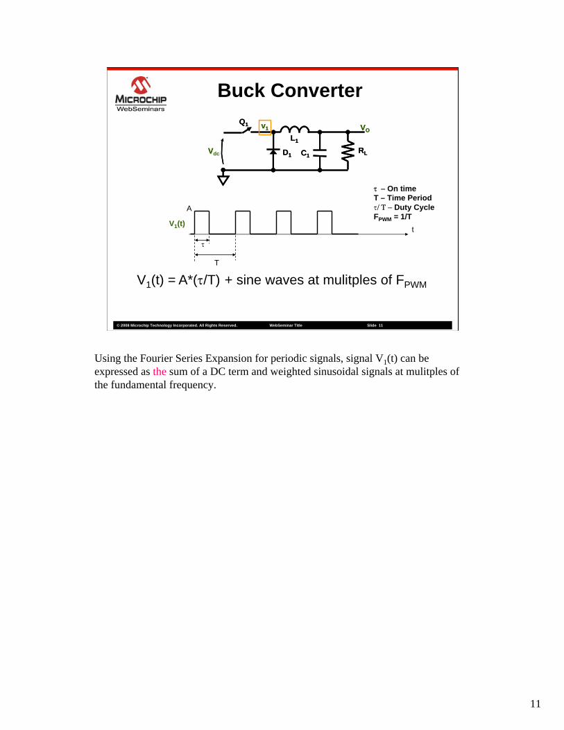
A*(τ/T) + sine waves at mulitples of FPWM
Using the Fourier Series Expansion for periodic signals, signal V1(t) can be expressed as the sum of a DC term and weighted sinusoidal signals at mulitples of the fundamental frequency.
12
© 2008 Microchip Technology Incorporated. All Rights Reserved. WebSeminar Title Slide 12
Buck Converter
V1(t) =
RL
VO
D1
v1
C1
L1
Vdc
Q1
RL
VO
D1
v1
C1
L1
V
Q1
τ
T
t
A
V1(t)
τ − On timeT – Time Periodτ/ Τ − Duty CycleFPWM = 1/T
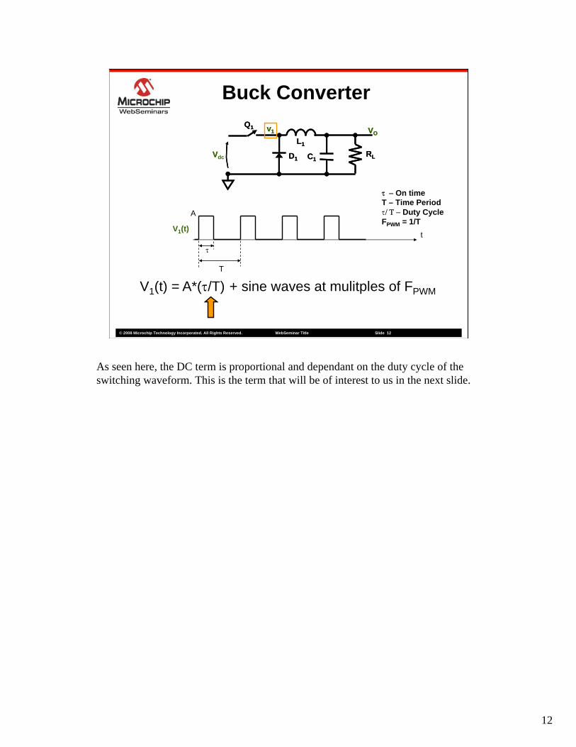
A*(τ/T) + sine waves at mulitples of FPWM
As seen here, the DC term is proportional and dependant on the duty cycle of the switching waveform. This is the term that will be of interest to us in the next slide.
13
© 2008 Microchip Technology Incorporated. All Rights Reserved. WebSeminar Title Slide 13
Buck Converter
RL
VO
D1
v1
C1
L1
Vdc
Q1
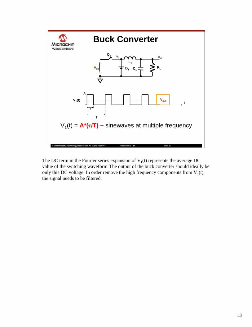
V1(t) = A*(τ/T) + sinewaves at multiple frequency
t
τ
T
Vave
A
VV11(t)(t)
The DC term in the Fourier series expansion of V1(t) represents the average DC value of the switching waveform. The output of the buck converter should ideally be only this DC voltage. In order remove the high frequency components from V1(t), the signal needs to be filtered.
14
© 2008 Microchip Technology Incorporated. All Rights Reserved. WebSeminar Title Slide 14
Buck Converter
RL
VO
D1
v1
C1
L1
Vdc
Q1
V1(t) = A*(τ/T) + sinewaves at multiple frequency
t
τ
T
Vave
A
VV11(t)(t)
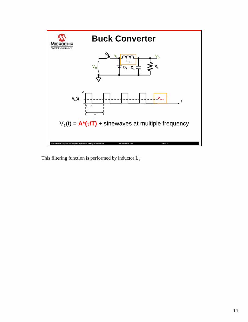
This filtering function is performed by inductor L1
15
© 2008 Microchip Technology Incorporated. All Rights Reserved. WebSeminar Title Slide 15
Buck Converter
RL
VO
D1
v1
C1
L1
Vdc
Q1
V1(t) = A*(τ/T) + sinewaves at multiple frequency
t
τ
T
Vave
A
VV11(t)(t)
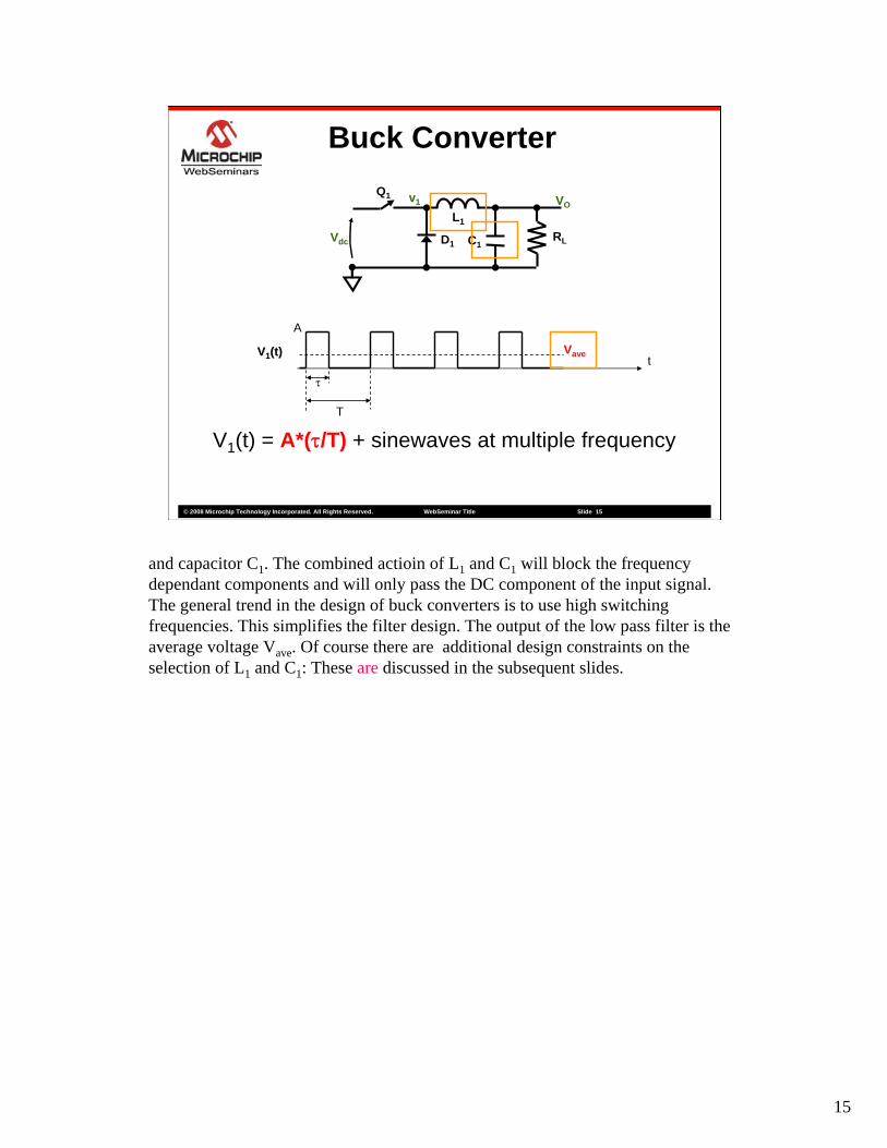
and capacitor C1. The combined actioin of L1 and C1 will block the frequency dependant components and will only pass the DC component of the input signal. The general trend in the design of buck converters is to use high switching frequencies. This simplifies the filter design. The output of the low pass filter is the average voltage Vave. Of course there are additional design constraints on the selection of L1 and C1: These are discussed in the subsequent slides.
16
© 2008 Microchip Technology Incorporated. All Rights Reserved. WebSeminar Title Slide 16
Buck Converter
RL
VO
D1
v1
C1
L1
Vdc
Q1
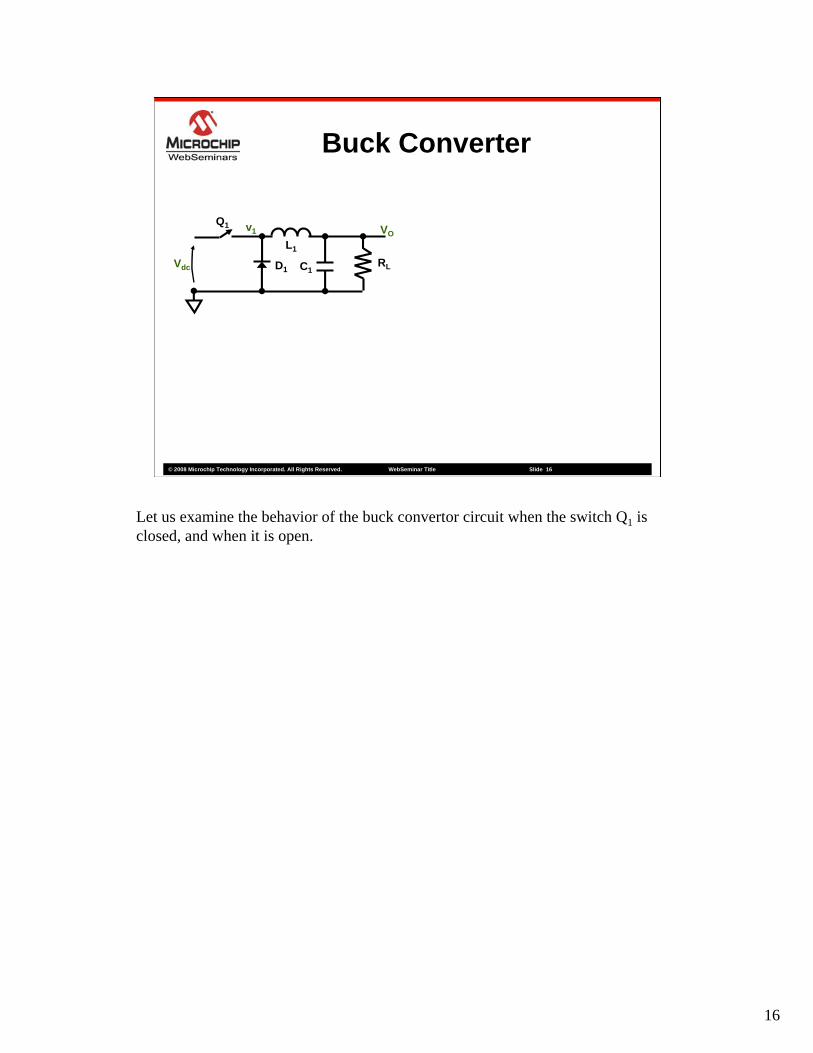
Let us examine the behavior of the buck convertor circuit when the switch Q1 is closed, and when it is open.
17
© 2008 Microchip Technology Incorporated. All Rights Reserved. WebSeminar Title Slide 17
Buck Converter
RL
VO
D1
v1
C1
L1
Vdc
Q1
Q1Q1cmdcmd
TON TOFF
T
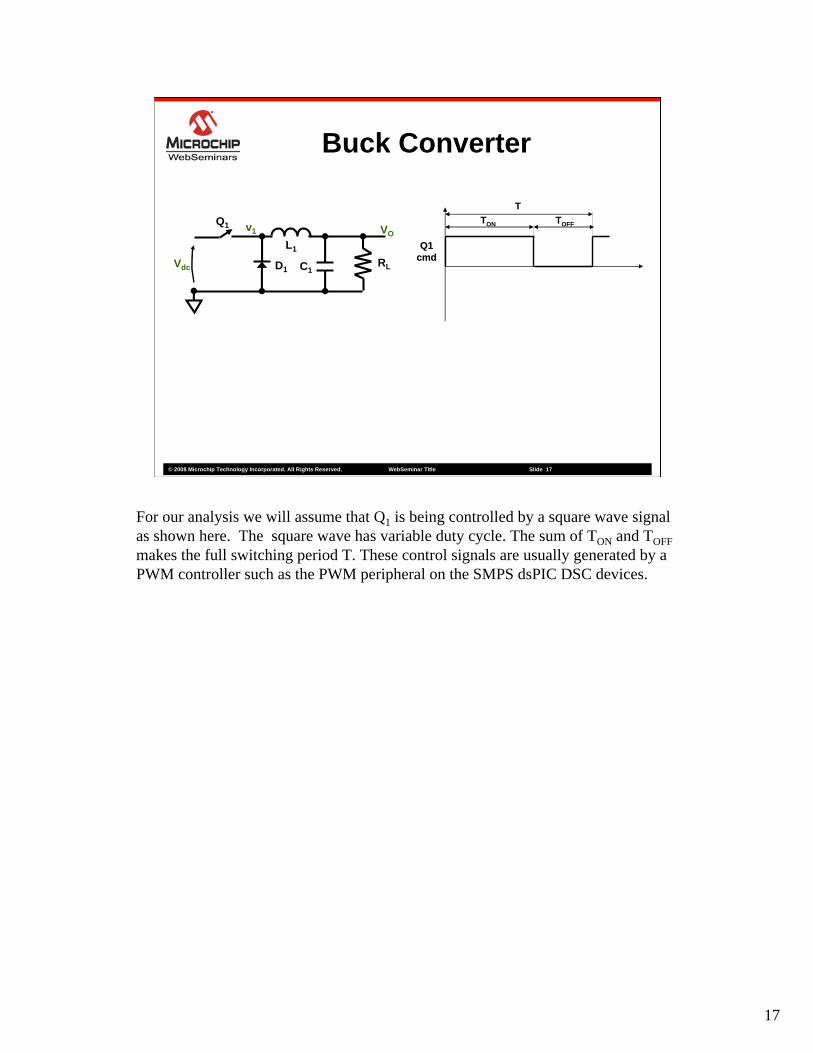
For our analysis we will assume that Q1 is being controlled by a square wave signal as shown here. The square wave has variable duty cycle. The sum of TON and TOFFmakes the full switching period T. These control signals are usually generated by a PWM controller such as the PWM peripheral on the SMPS dsPIC DSC devices.
18
© 2008 Microchip Technology Incorporated. All Rights Reserved. WebSeminar Title Slide 18
Buck Converter
RL
VO
D1
v1
C1
L1
Vdc
Q1
Q1Q1cmdcmd
TON TOFF
T
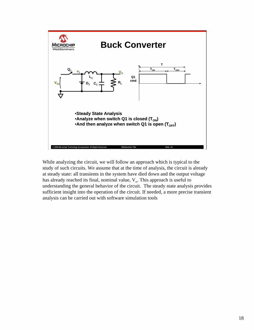
••Steady State AnalysisSteady State Analysis••Analyze when switch Q1 is closed (TAnalyze when switch Q1 is closed (TONON))••And then analyze when switch Q1 is open (TAnd then analyze when switch Q1 is open (TOFFOFF))
While analyzing the circuit, we will follow an approach which is typical to the study of such circuits. We assume that at the time of analysis, the circuit is already at steady state: all transients in the system have died down and the output voltage has already reached its final, nominal value, Vo. This approach is useful to understanding the general behavior of the circuit. The steady state analysis provides sufficient insight into the operation of the circuit. If needed, a more precise transient analysis can be carried out with software simulation tools
19
© 2008 Microchip Technology Incorporated. All Rights Reserved. WebSeminar Title Slide 19
Buck Converter
RL
VO
D1
v1
C1
L1
Vdc
Q1 Q1Q1cmdcmd
TON TOFF
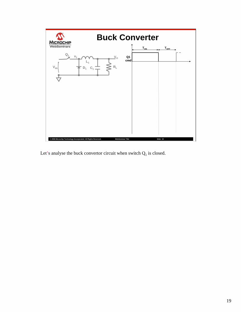
Let’s analyse the buck convertor circuit when switch Q1 is closed.
20
© 2008 Microchip Technology Incorporated. All Rights Reserved. WebSeminar Title Slide 20
Buck Converter
RL
VO
D1
v1
C1
L1
Vdc
Q1 Q1Q1cmdcmd
TON TOFF
vLQ1 on
RL
VO
D1
v1
C1
L1
Vdc
Q1++ --
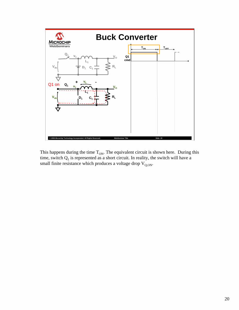
This happens during the time TON. The equivalent circuit is shown here. During this time, switch Q1 is represented as a short circuit. In reality, the switch will have a small finite resistance which produces a voltage drop VQ,ON.
21
© 2008 Microchip Technology Incorporated. All Rights Reserved. WebSeminar Title Slide 21
Buck Converter
RL
VO
D1
v1
C1
L1
Vdc
Q1 Q1Q1cmdcmd
TON TOFF
vLQ1 on
RL
VO
D1
v1
C1
L1
Vdc
Q1++ --
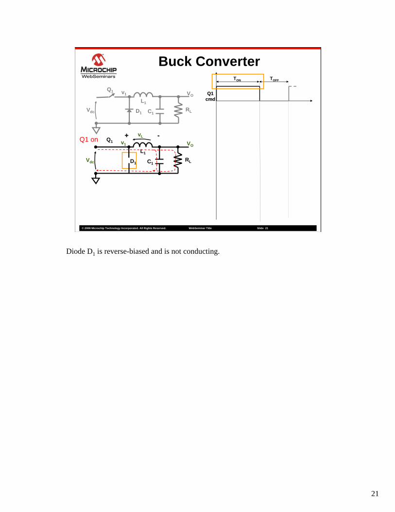
Diode D1 is reverse-biased and is not conducting.

22
© 2008 Microchip Technology Incorporated. All Rights Reserved. WebSeminar Title Slide 22
Buck Converter
RL
VO
D1
v1
C1
L1
Vdc
Q1 Q1Q1cmdcmd
TON TOFF
vLQ1 on
RL
VO
D1
v1
C1
L1
Vdc
Q1++ --
The left side of the inductor is more positive

23
© 2008 Microchip Technology Incorporated. All Rights Reserved. WebSeminar Title Slide 23
Buck Converter
RL
VO
D1
v1
C1
L1
Vdc
Q1 Q1Q1cmdcmd
TON TOFF
vLQ1 on
RL
VO
D1
v1
C1
L1
Vdc
Q1++ --
than the right side.
24
© 2008 Microchip Technology Incorporated. All Rights Reserved. WebSeminar Title Slide 24
Buck Converter
RL
VO
D1
v1
C1
L1
Vdc
Q1 Q1Q1cmdcmd
TON TOFF
VVLL
VL= Vdc – VQ,ON - Vo
oonQdcL VVVv −−= ,
vLQ1 on
RL
VO
D1
v1
C1
L1
Vdc
Q1++ --
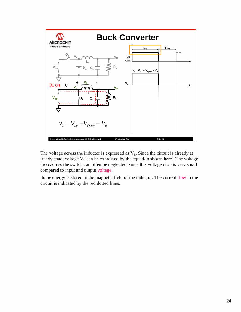
The voltage across the inductor is expressed as VL. Since the circuit is already at steady state, voltage VL can be expressed by the equation shown here. The voltage drop across the switch can often be neglected, since this voltage drop is very small compared to input and output voltage.Some energy is stored in the magnetic field of the inductor. The current flow in the circuit is indicated by the red dotted lines.
25
© 2008 Microchip Technology Incorporated. All Rights Reserved. WebSeminar Title Slide 25
Buck Converter
RL
VO
D1
v1
C1
L1
Vdc
Q1 Q1Q1cmdcmd
TON TOFF
VVLL
VL= Vdc – VQ,ON - Vo
oonQdcL VVVv −−= ,
vLQ1 on
RL
VO
D1
v1
C1
L1
Vdc
Q1++ --
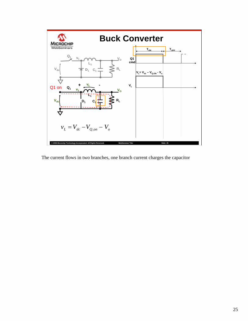
The current flows in two branches, one branch current charges the capacitor

26
© 2008 Microchip Technology Incorporated. All Rights Reserved. WebSeminar Title Slide 26
Buck Converter
RL
VO
D1
v1
C1
L1
Vdc
Q1 Q1Q1cmdcmd
TON TOFF
VVLL
VL= Vdc – VQ,ON - Vo
oonQdcL VVVv −−= ,
vLQ1 on
RL
VO
D1
v1
C1
L1
Vdc
Q1++ --
while the other branch current flows through the load.
27
© 2008 Microchip Technology Incorporated. All Rights Reserved. WebSeminar Title Slide 27
Buck Converter
RL
VO
D1
v1
C1
L1
Vdc
Q1vL
Q1 on
RL
VO
D1
v1
C1
L1
Vdc
Q1vL
Q1Q1cmdcmd
VVLL
TON TOFF
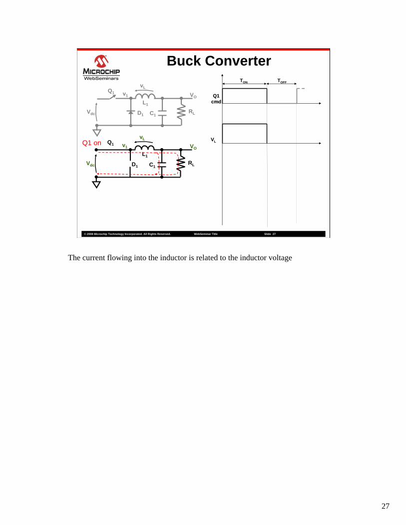
The current flowing into the inductor is related to the inductor voltage
28
© 2008 Microchip Technology Incorporated. All Rights Reserved. WebSeminar Title Slide 28
Buck Converter
RL
VO
D1
v1
C1
L1
Vdc
Q1vL
Q1 on
RL
VO
D1
v1
C1
L1
Vdc
Q1vL
Q1Q1cmdcmd
VVLL
TON TOFF
tL
VVViti oonQdcLL
1
,)0()(−−
+=
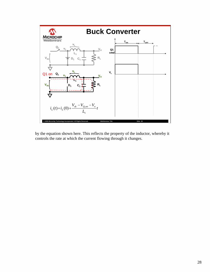
by the equation shown here. This reflects the property of the inductor, whereby it controls the rate at which the current flowing through it changes.

29
© 2008 Microchip Technology Incorporated. All Rights Reserved. WebSeminar Title Slide 29
Buck Converter
RL
VO
D1
v1
C1
L1
Vdc
Q1vL
Q1 on
RL
VO
D1
v1
C1
L1
Vdc
Q1vL
Q1Q1cmdcmd
VVLL
TON TOFF
tL
VVViti oonQdcLL
1
,)0()(−−
+=IILL
0 TON T
The inductor current displays a linear behavior with a rising slope during time TON. We will see later as to why the inductor current generally does not start from zero at the beginning of the period.
30
© 2008 Microchip Technology Incorporated. All Rights Reserved. WebSeminar Title Slide 30
Buck Converter
RL
VO
D1
v1
C1
L1
Vdc
Q1vL
Q1 on
RL
VO
D1
v1
C1
L1
Vdc
Q1vL
oonQdcL VVVv −−= ,
( )t
LVVV
iti oonQdcLL
1
,)0()(−−
+=
( )on
oonQdcLonL T
LVVV
iTi1
,)0()(−−
+=
Inductor Voltage:
Inductor Current:
Inductor Current at TON:
Topology Equations
……Eq. 1Eq. 1
……Eq. 2Eq. 2
……Eq. 3Eq. 3
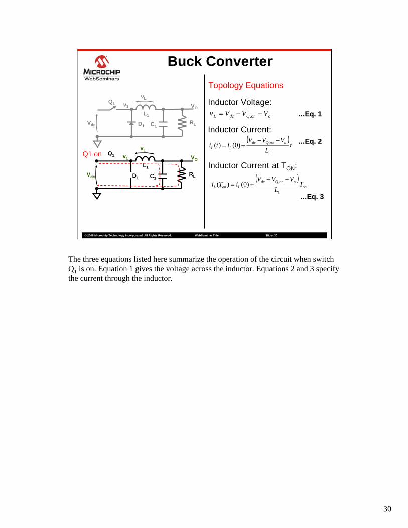
The three equations listed here summarize the operation of the circuit when switch Q1 is on. Equation 1 gives the voltage across the inductor. Equations 2 and 3 specify the current through the inductor.
31
© 2008 Microchip Technology Incorporated. All Rights Reserved. WebSeminar Title Slide 31
Buck Converter
RL
VO
D1
v1
C1
L1
Vdc
Q1vL
Q1 on
RL
VO
D1
v1
C1
L1
Vdc
Q1vL
Q1Q1cmdcmd
VVLL
TON TOFF
vLQ1 off
RL
VO
D1
v1
C1
L1
Vdc
Q1
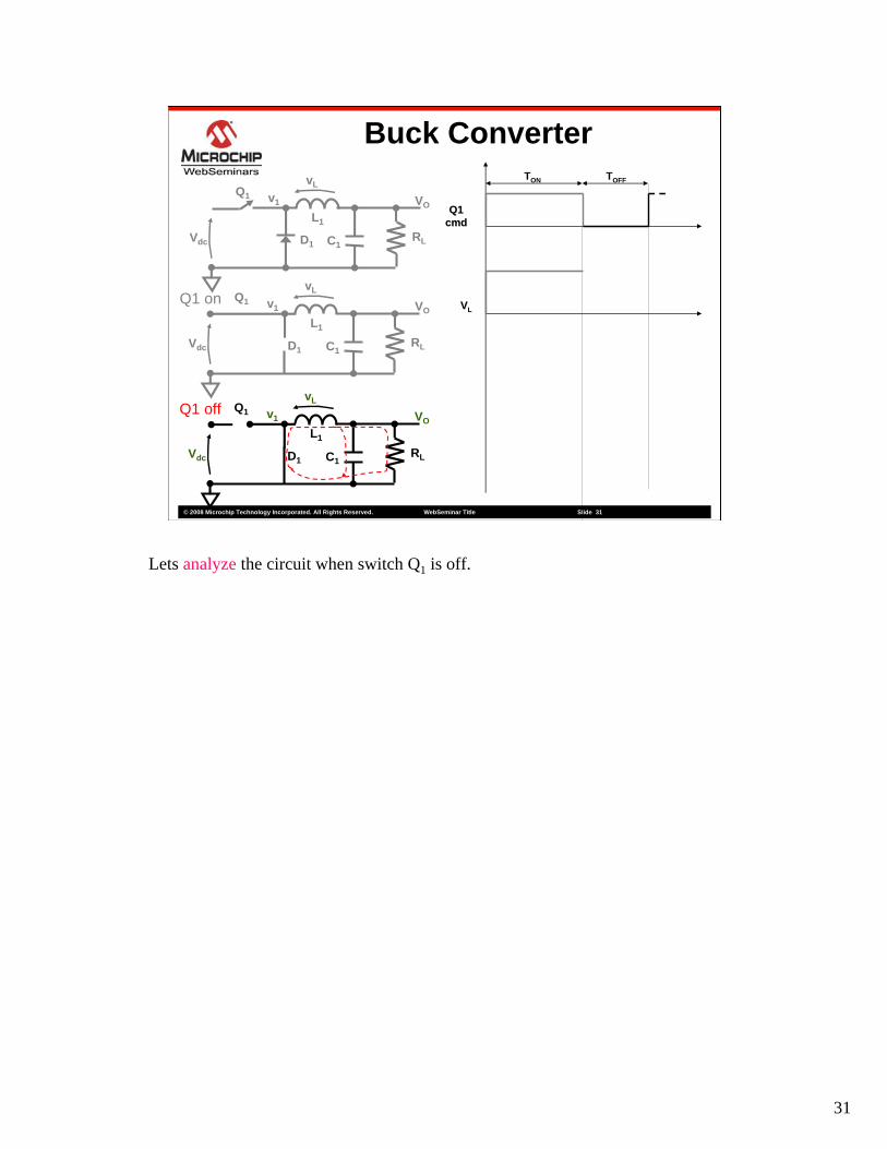
Lets analyze the circuit when switch Q1 is off.
32
© 2008 Microchip Technology Incorporated. All Rights Reserved. WebSeminar Title Slide 32
Buck Converter
RL
VO
D1
v1
C1
L1
Vdc
Q1vL
Q1 on
RL
VO
D1
v1
C1
L1
Vdc
Q1vL
Q1Q1cmdcmd
VVLL
vLQ1 off
RL
VO
D1
v1
C1
L1
Vdc
Q1
TON TOFF
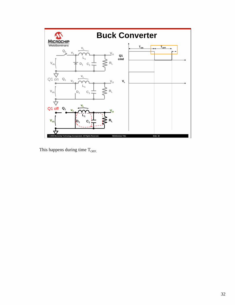
This happens during time TOFF.
33
© 2008 Microchip Technology Incorporated. All Rights Reserved. WebSeminar Title Slide 33
Buck Converter
RL
VO
D1
v1
C1
L1
Vdc
Q1vL
Q1 on
RL
VO
D1
v1
C1
L1
Vdc
Q1vL
Q1Q1cmdcmd
VVLL
vLQ1 off
RL
VO
D1
v1
C1
L1
Vdc
Q1
TON TOFF
VL= -Vo – VD,on
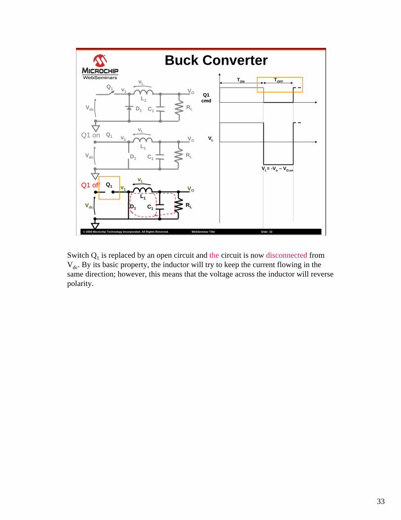
Switch Q1 is replaced by an open circuit and the circuit is now disconnected from Vdc. By its basic property, the inductor will try to keep the current flowing in the same direction; however, this means that the voltage across the inductor will reverse polarity.

34
© 2008 Microchip Technology Incorporated. All Rights Reserved. WebSeminar Title Slide 34
Buck Converter
RL
VO
D1
v1
C1
L1
Vdc
Q1vL
Q1 on
RL
VO
D1
v1
C1
L1
Vdc
Q1vL
Q1Q1cmdcmd
VVLL
vLQ1 off
RL
VO
D1
v1
C1
L1
Vdc
Q1
TON TOFF
VL= -Vo – VD,on
++
Now, the right side
35
© 2008 Microchip Technology Incorporated. All Rights Reserved. WebSeminar Title Slide 35
Buck Converter
RL
VO
D1
v1
C1
L1
Vdc
Q1vL
Q1 on
RL
VO
D1
v1
C1
L1
Vdc
Q1vL
Q1Q1cmdcmd
VVLL
vLQ1 off
RL
VO
D1
v1
C1
L1
Vdc
Q1
TON TOFF
VL= -Vo – VD,on
-- ++
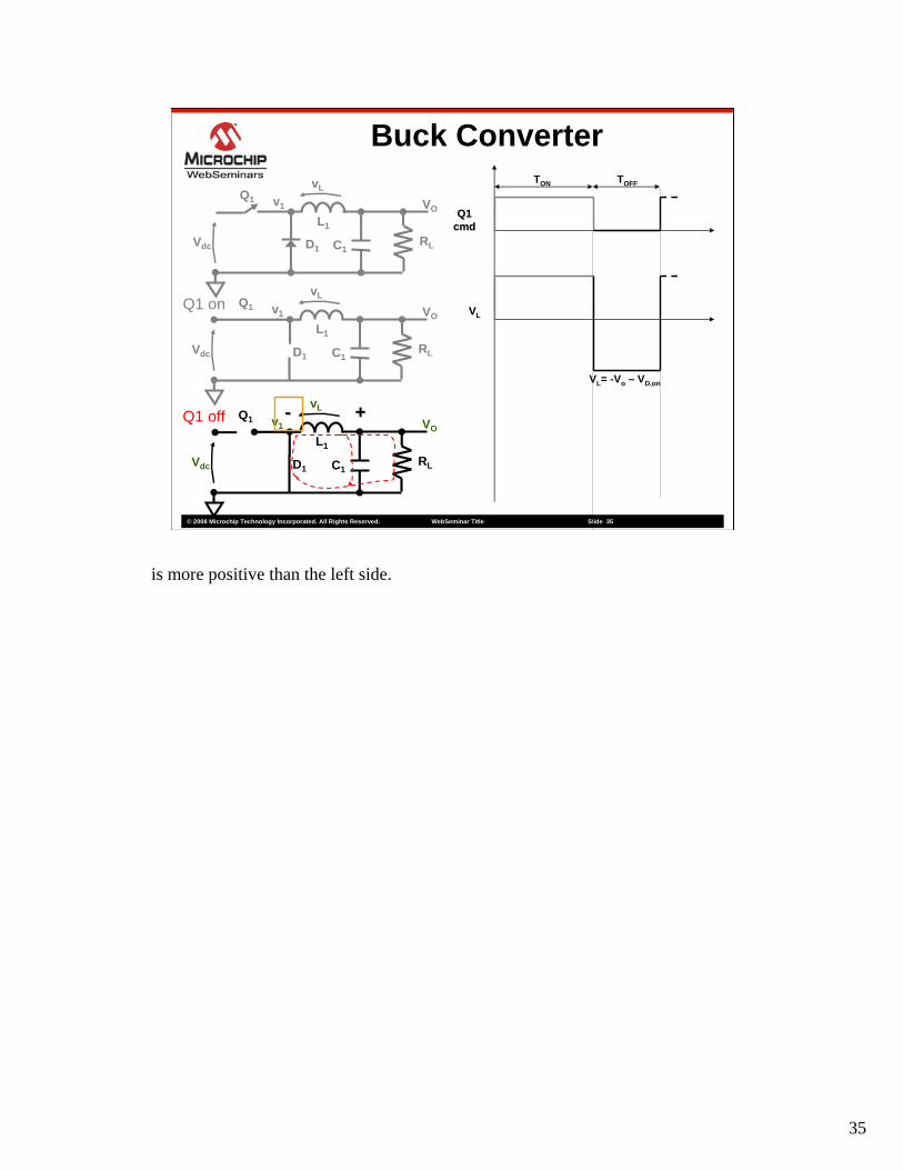
is more positive than the left side.
36
© 2008 Microchip Technology Incorporated. All Rights Reserved. WebSeminar Title Slide 36
Buck Converter
RL
VO
D1
v1
C1
L1
Vdc
Q1vL
Q1 on
RL
VO
D1
v1
C1
L1
Vdc
Q1vL
Q1Q1cmdcmd
VVLL
vLQ1 off
RL
VO
D1
v1
C1
L1
Vdc
Q1
TON TOFF
D,onoL VVv −−=
VL= -Vo – VD,on
-- ++
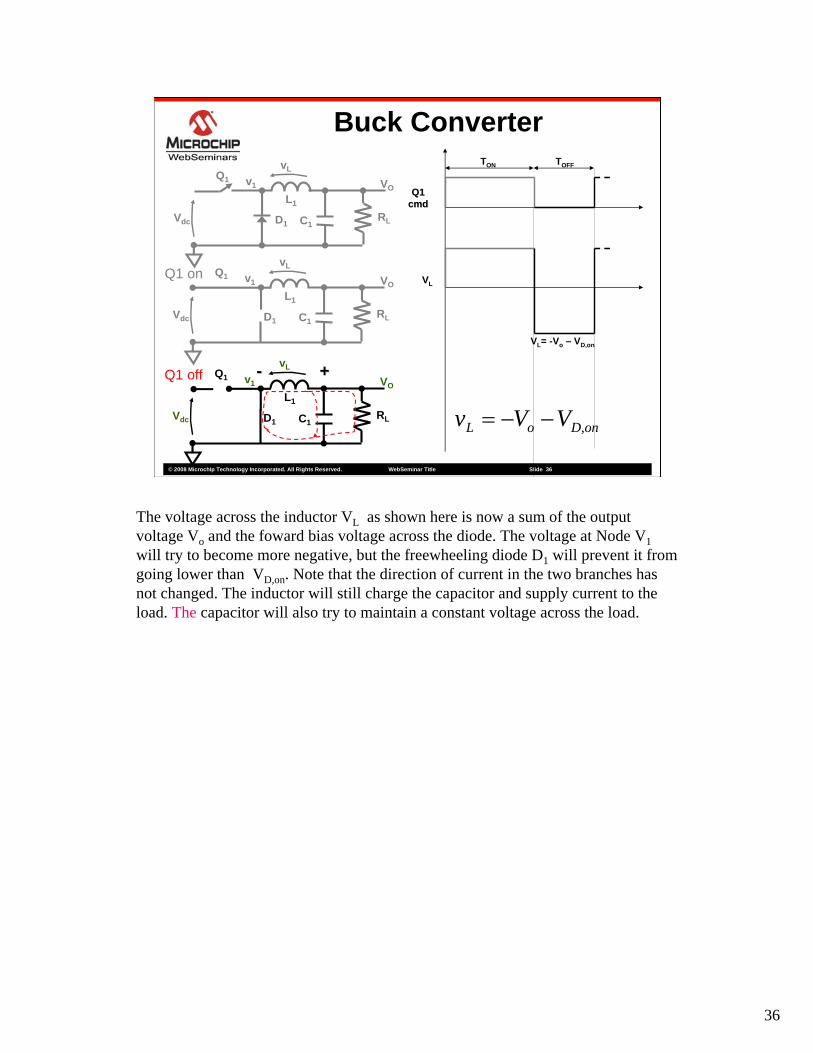
The voltage across the inductor VL as shown here is now a sum of the output voltage Vo and the foward bias voltage across the diode. The voltage at Node V1will try to become more negative, but the freewheeling diode D1 will prevent it from going lower than VD,on. Note that the direction of current in the two branches has not changed. The inductor will still charge the capacitor and supply current to the load. The capacitor will also try to maintain a constant voltage across the load.
37
© 2008 Microchip Technology Incorporated. All Rights Reserved. WebSeminar Title Slide 37
Buck Converter
RL
VO
D1
v1
C1
L1
Vdc
Q1vL
Q1 on
RL
VO
D1
v1
C1
L1
Vdc
Q1vL
vLQ1 off
RL
VO
D1
v1
C1
L1
Vdc
Q1
Q1Q1cmdcmd
VVLL
IILL
TON TOFF
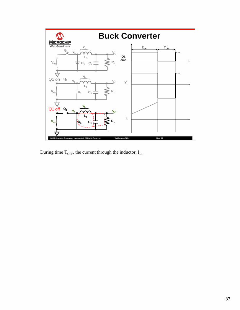
During time TOFF, the current through the inductor, IL,
38
© 2008 Microchip Technology Incorporated. All Rights Reserved. WebSeminar Title Slide 38
Buck Converter
RL
VO
D1
v1
C1
L1
Vdc
Q1vL
Q1 on
RL
VO
D1
v1
C1
L1
Vdc
Q1vL
vLQ1 off
RL
VO
D1
v1
C1
L1
Vdc
Q1
Q1Q1cmdcmd
VVLL
IILL
TON TOFF
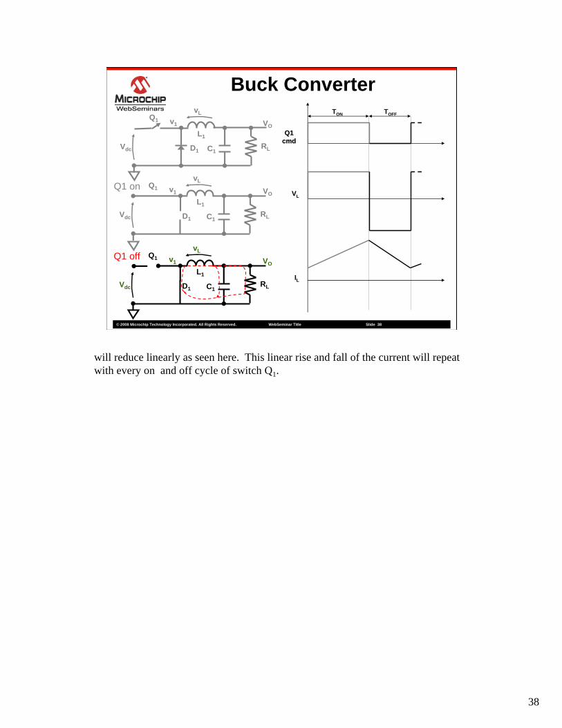
will reduce linearly as seen here. This linear rise and fall of the current will repeat with every on and off cycle of switch Q1.
39
© 2008 Microchip Technology Incorporated. All Rights Reserved. WebSeminar Title Slide 39
Buck Converter
RL
VO
D1
v1
C1
L1
Vdc
Q1vL
Q1 on
RL
VO
D1
v1
C1
L1
Vdc
Q1vL
vLQ1 off
RL
VO
D1
v1
C1
L1
Vdc
Q1
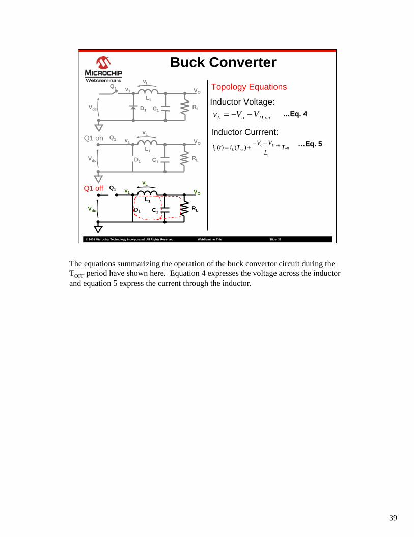
onDoL VVv ,−−=
Topology Equations
Inductor Voltage:
Inductor Currrent:
offonDo
onLL TL
VVTiti
1
,)()(−−
+=
……Eq. 4Eq. 4
……Eq. 5Eq. 5
The equations summarizing the operation of the buck convertor circuit during the TOFF period have shown here. Equation 4 expresses the voltage across the inductor and equation 5 express the current through the inductor.

40
© 2008 Microchip Technology Incorporated. All Rights Reserved. WebSeminar Title Slide 40
Buck Converter –Current Ripple
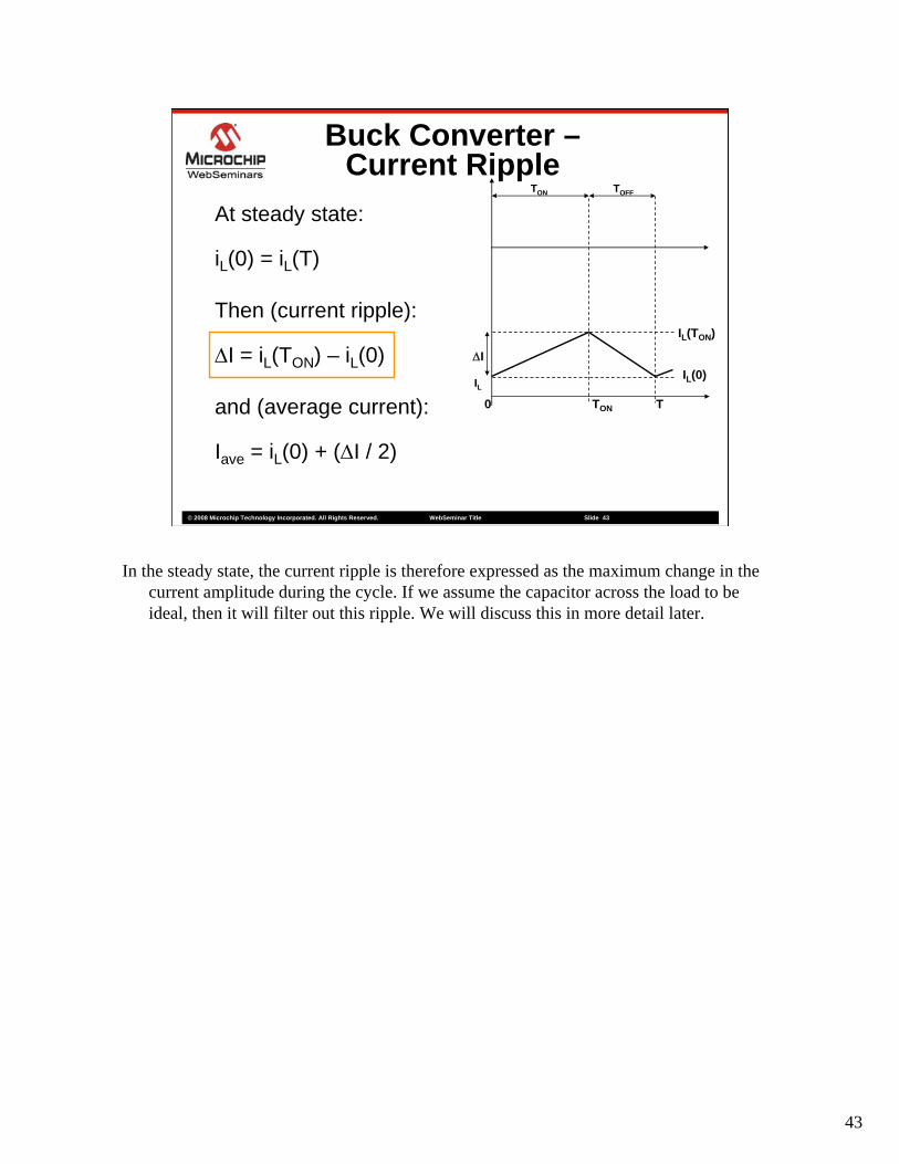
At steady state:
iL(0) = iL(T)
Then (current ripple):
ΔI = iL(TON) – iL(0)
and (average current):
Iave = iL(0) + (ΔI / 2)
IILL
ΔI
TON TOFF
0 TON T
IL(0)
IL(TON)
Let’s analyze the current flowing through the inductor during each PWM period. We will again take advantage of performing steady state analysis of the circuit.

41
© 2008 Microchip Technology Incorporated. All Rights Reserved. WebSeminar Title Slide 41
Buck Converter –Current Ripple
At steady state:
iL(0) = iL(T)
Then (current ripple):
ΔI = iL(TON) – iL(0)
and (average current):
Iave = iL(0) + (ΔI / 2)
IILL
ΔI
TON TOFF
0 TON T
IL(0)
IL(TON)
In this condition, the current flowing into the inductor at the beginning of each pwm period

42
© 2008 Microchip Technology Incorporated. All Rights Reserved. WebSeminar Title Slide 42
Buck Converter –Current Ripple
At steady state:
iL(0) = iL(T)
Then (current ripple):
ΔI = iL(TON) – iL(0)
and (average current):
Iave = iL(0) + (ΔI / 2)
IILL
ΔI
TON TOFF
0 TON T
IL(0)
IL(TON)
must equal the current at the following end of the period. If this is not true, it means that the system has not yet reached a steady state condition , or some kind of perturbation has occurred.
43
© 2008 Microchip Technology Incorporated. All Rights Reserved. WebSeminar Title Slide 43
Buck Converter –Current Ripple
At steady state:
iL(0) = iL(T)
Then (current ripple):
ΔI = iL(TON) – iL(0)
and (average current):
Iave = iL(0) + (ΔI / 2)
IILL
ΔI
TON TOFF
0 TON T
IL(0)
IL(TON)
In the steady state, the current ripple is therefore expressed as the maximum change in the current amplitude during the cycle. If we assume the capacitor across the load to be ideal, then it will filter out this ripple. We will discuss this in more detail later.

44
© 2008 Microchip Technology Incorporated. All Rights Reserved. WebSeminar Title Slide 44
Buck Converter –Current Ripple
At steady state:
iL(0) = iL(T)
Then (current ripple):
ΔI = iL(TON) – iL(0)
and (average current):
Iave = iL(0) + (ΔI / 2)
IILL
ΔI
TON TOFF
0 TON T
IL(0)
IL(TON)
The average value of the inductor current is then expressed as the sum of the current at the beginning of the period and one/half of the ripple value. By the virtue of this topology, the average current flowing through the inductor is also the average current flowing though the load.
45
© 2008 Microchip Technology Incorporated. All Rights Reserved. WebSeminar Title Slide 45
Buck Converter – Input/Output Relationship
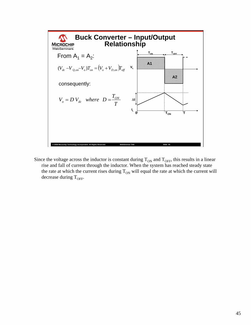
From A1 = A2:
IILL
ΔI
VVLL( ) offonDoonoonQdc TVVTVVV ,, )( +=−−
TON TOFF
consequently:
TTDwhereVDV ON
dco ==
0 TON T
A1
A2
Since the voltage across the inductor is constant during TON and TOFF, this results in a linear rise and fall of current through the inductor. When the system has reached steady state the rate at which the current rises during TON will equal the rate at which the current will decrease during TOFF.
46
© 2008 Microchip Technology Incorporated. All Rights Reserved. WebSeminar Title Slide 46
Buck Converter – Input/Output Relationship
From A1 = A2:
IILL
ΔI
VVLL( ) offonDoonoonQdc TVVTVVV ,, )( +=−−
TON TOFF
consequently:
TTDwhereVDV ON
dco ==
0 TON T
A1
A2
This also implies that area A1

47
© 2008 Microchip Technology Incorporated. All Rights Reserved. WebSeminar Title Slide 47
Buck Converter – Input/Output Relationship
From A1 = A2:
IILL
ΔI
VVLL( ) offonDoonoonQdc TVVTVVV ,, )( +=−−
TON TOFF
consequently:
TTDwhereVDV ON
dco ==
0 TON T
A1
A2
must equal area A2.
48
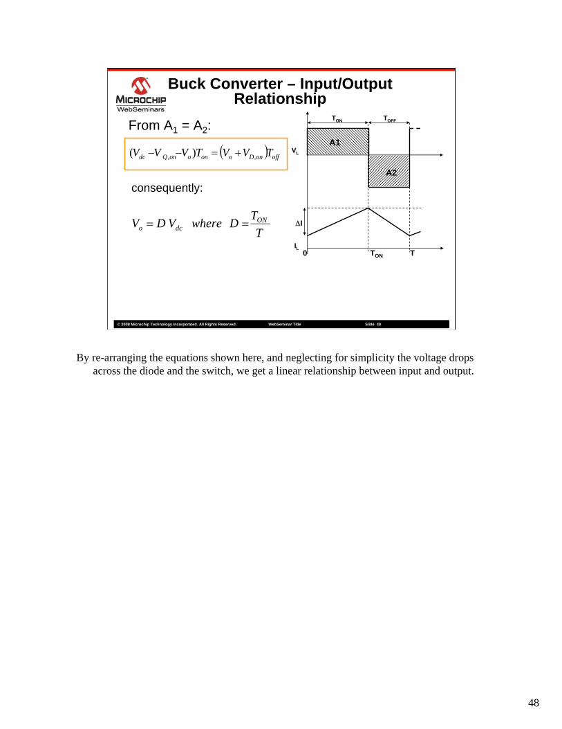
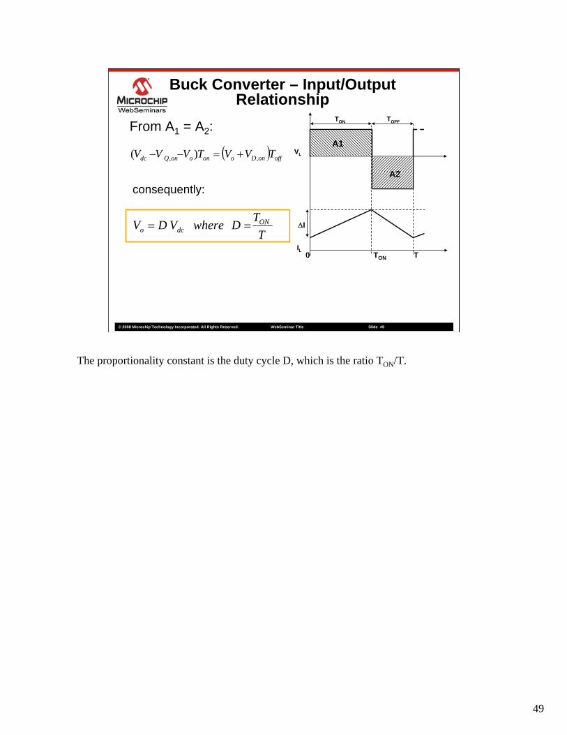
© 2008 Microchip Technology Incorporated. All Rights Reserved. WebSeminar Title Slide 48
Buck Converter – Input/Output Relationship
From A1 = A2:
IILL
ΔI
VVLL( ) offonDoonoonQdc TVVTVVV ,, )( +=−−
TON TOFF
consequently:
TTDwhereVDV ON
dco ==
0 TON T
A1
A2
By re-arranging the equations shown here, and neglecting for simplicity the voltage drops across the diode and the switch, we get a linear relationship between input and output.
49
© 2008 Microchip Technology Incorporated. All Rights Reserved. WebSeminar Title Slide 49
Buck Converter – Input/Output Relationship
From A1 = A2:
IILL
ΔI
VVLL( ) offonDoonoonQdc TVVTVVV ,, )( +=−−
TON TOFF
consequently:
TTDwhereVDV ON
dco ==
0 TON T
A1
A2
The proportionality constant is the duty cycle D, which is the ratio TON/T.

50
© 2008 Microchip Technology Incorporated. All Rights Reserved. WebSeminar Title Slide 50
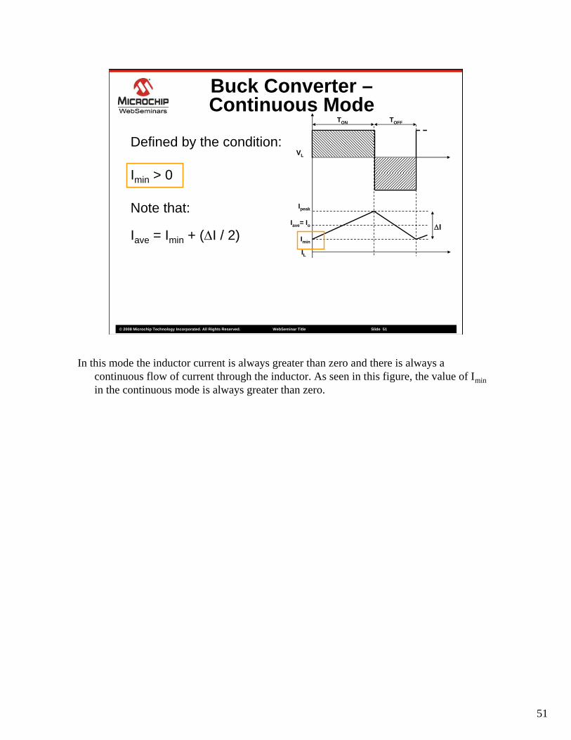
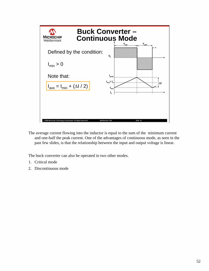
Buck Converter –Continuous Mode
Defined by the condition:
Imin > 0
Note that:
Iave = Imin + (ΔI / 2)IILL
ΔI
VVLL
TON TOFF
Ipeak
Iave= Io
Imin
So far, we have discussed the operation of the buck converter circuit in the so-called Continuous mode.
51
© 2008 Microchip Technology Incorporated. All Rights Reserved. WebSeminar Title Slide 51
Buck Converter –Continuous Mode
Defined by the condition:
Imin > 0
Note that:
Iave = Imin + (ΔI / 2)IILL
ΔI
VVLL
TON TOFF
Ipeak
Iave= Io
Imin
In this mode the inductor current is always greater than zero and there is always a continuous flow of current through the inductor. As seen in this figure, the value of Imin in the continuous mode is always greater than zero.
52
© 2008 Microchip Technology Incorporated. All Rights Reserved. WebSeminar Title Slide 52
Buck Converter –Continuous Mode
Defined by the condition:
Imin > 0
Note that:
Iave = Imin + (ΔI / 2)IILL
ΔI
VVLL
TON TOFF
Ipeak
Iave= Io
Imin
The average current flowing into the inductor is equal to the sum of the minimum current and one-half the peak current. One of the advantages of continuous mode, as seen in the past few slides, is that the relationship between the input and output voltage is linear.
The buck converter can also be operated in two other modes.1. Critical mode2. Discontinuous mode
53
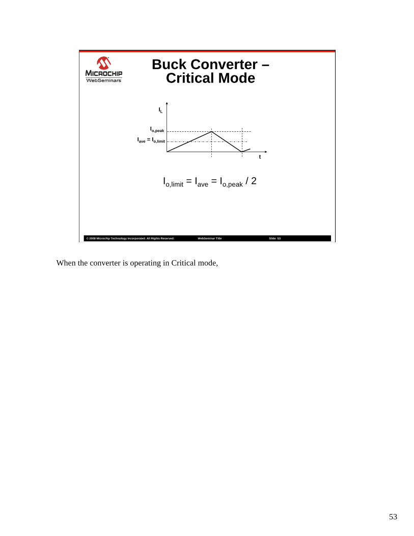
© 2008 Microchip Technology Incorporated. All Rights Reserved. WebSeminar Title Slide 53
Buck Converter –Critical Mode
Io,limit = Iave = Io,peak / 2
Iave = Io,limit
Io,peak
IL
t
When the converter is operating in Critical mode,

54
© 2008 Microchip Technology Incorporated. All Rights Reserved. WebSeminar Title Slide 54
Buck Converter –Critical Mode
Io,limit = Iave = Io,peak / 2
Iave = Io,limit
Io,peak
IL
t
the inductor current reaches zero at the beginning and the end of each PWM period.
55
© 2008 Microchip Technology Incorporated. All Rights Reserved. WebSeminar Title Slide 55
Buck Converter –Critical Mode
Io,limit = Iave = Io,peak / 2
Iave = Io,limit
Io,peak
IL
t
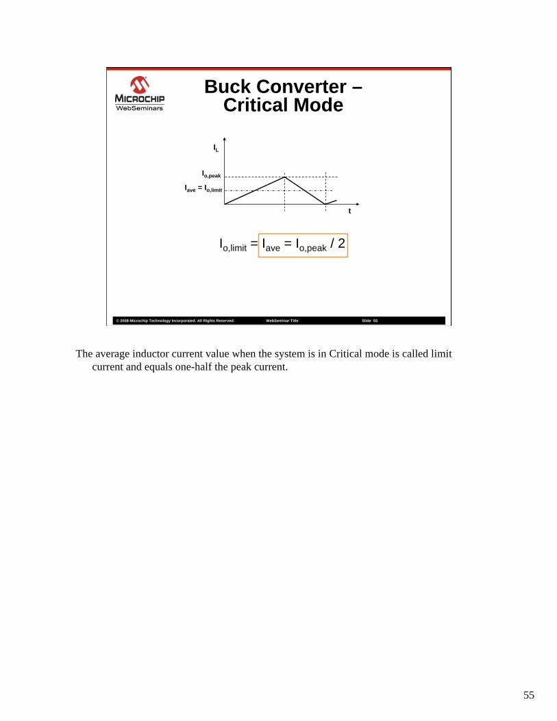
The average inductor current value when the system is in Critical mode is called limit current and equals one-half the peak current.
56
© 2008 Microchip Technology Incorporated. All Rights Reserved. WebSeminar Title Slide 56
Buck Converter –Discontinuous Mode
Critical Mode
Io,limit
Io,peak
IL
t
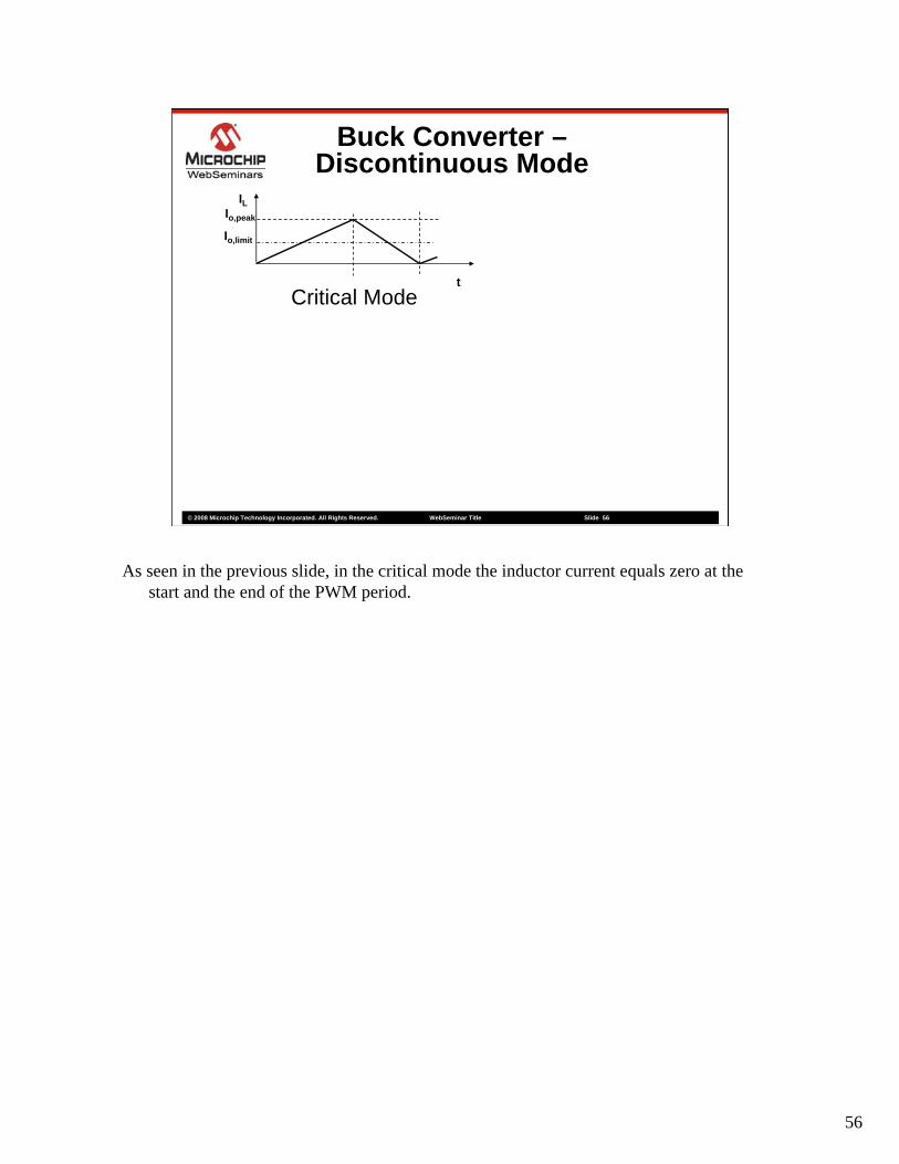
As seen in the previous slide, in the critical mode the inductor current equals zero at the start and the end of the PWM period.
57
© 2008 Microchip Technology Incorporated. All Rights Reserved. WebSeminar Title Slide 57
Buck Converter –Discontinuous Mode
Critical Mode
Io,limit
Io,peak
IL
t
Io,limitIo,ave
Discontinuous Mode
IL
t
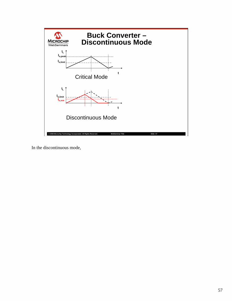
In the discontinuous mode,

58
© 2008 Microchip Technology Incorporated. All Rights Reserved. WebSeminar Title Slide 58
Buck Converter –Discontinuous Mode
Critical Mode
Io,limit
Io,peak
IL
t
Io,limitIo,ave
Discontinuous Mode
IL
t
the inductor current reaches zero
59
© 2008 Microchip Technology Incorporated. All Rights Reserved. WebSeminar Title Slide 59
Buck Converter –Discontinuous Mode
Critical Mode
Io,limit
Io,peak
IL
t
Io,limitIo,ave
Discontinuous Mode
IL
t
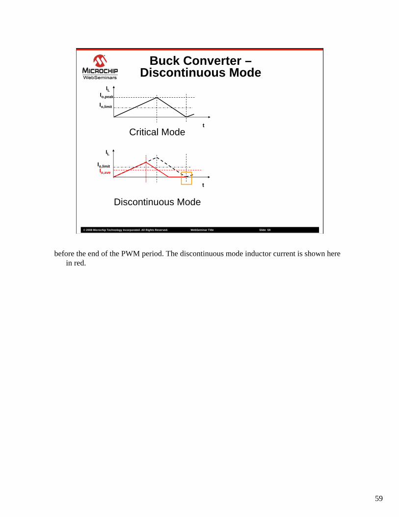
before the end of the PWM period. The discontinuous mode inductor current is shown here in red.
60
© 2008 Microchip Technology Incorporated. All Rights Reserved. WebSeminar Title Slide 60
Buck Converter –Discontinuous Mode
Critical Mode
Io,limit
Io,peak
IL
t
Io,limitIo,ave
Discontinuous Mode
IL
t
( )itoodc
o
IID
DVV
lim,2
2
41
+=
Input / Output Relationship
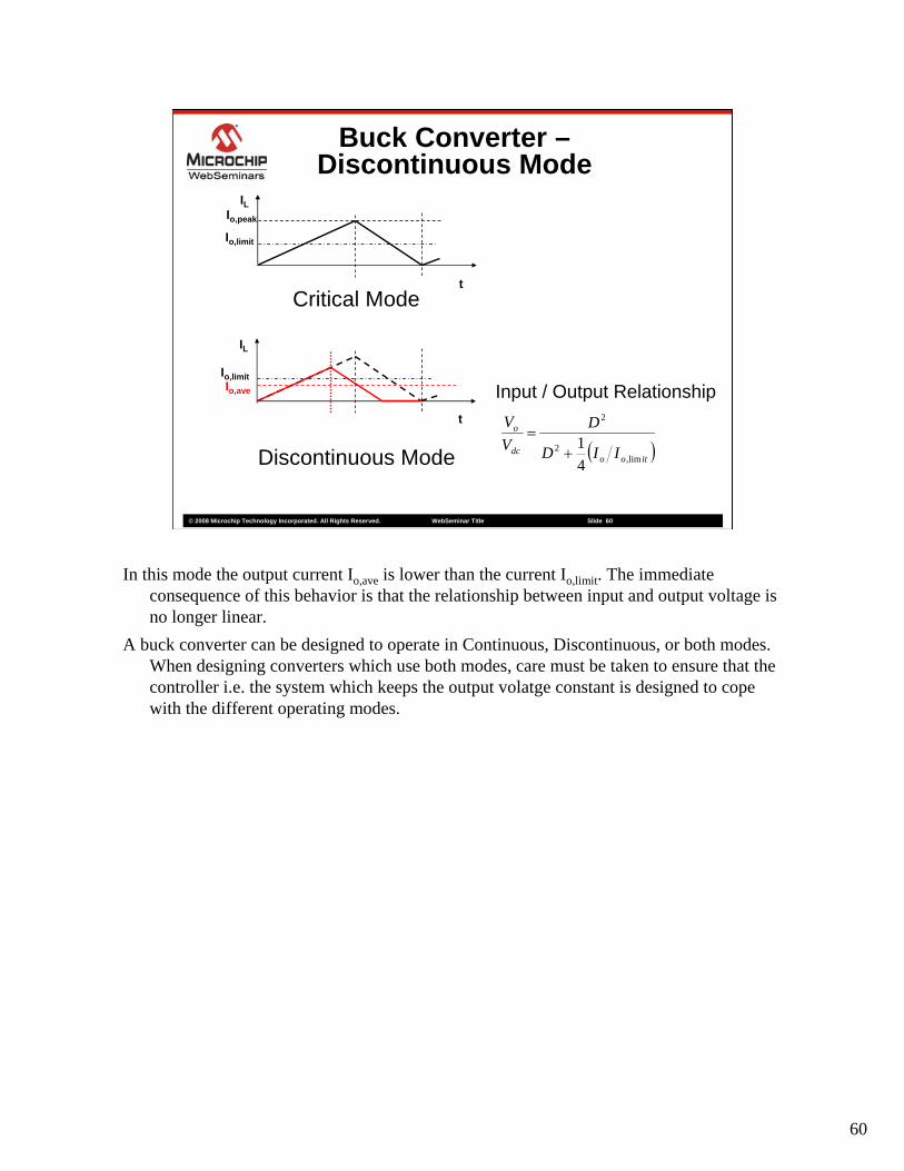
In this mode the output current Io,ave is lower than the current Io,limit. The immediate consequence of this behavior is that the relationship between input and output voltage is no longer linear.
A buck converter can be designed to operate in Continuous, Discontinuous, or both modes. When designing converters which use both modes, care must be taken to ensure that the controller i.e. the system which keeps the output volatge constant is designed to cope with the different operating modes.

61
© 2008 Microchip Technology Incorporated. All Rights Reserved. WebSeminar Title Slide 61
Buck Converter - Design
Known QuantitiesVdcmin and Vdcmax
Required output Voltage Vo
Nominal load current Io,av,nom
PWM Frequency FPWM
Maximum Allowable Output Ripple.
We will now discuss the design of a buck converter, that is determining the components values. Before we start, we need to specify some data which will guide our design. We need to specify the minimum and maximum input voltage, output voltage , the required load current, the PWM frequency and finally the acceptable value of output ripple.
62
© 2008 Microchip Technology Incorporated. All Rights Reserved. WebSeminar Title Slide 62
Buck Converter Design –Duty Cycle limit
Input-output relation:
IILL
ΔI
VVLL( ) offonDoonoonQdc TVVTVVV ,, )( +=−−
TON TOFF
min,max
dc
o
VVD =
consequently:
Maximum duty cyle:T
TDwhereVDV ONdco ==
0 TON T
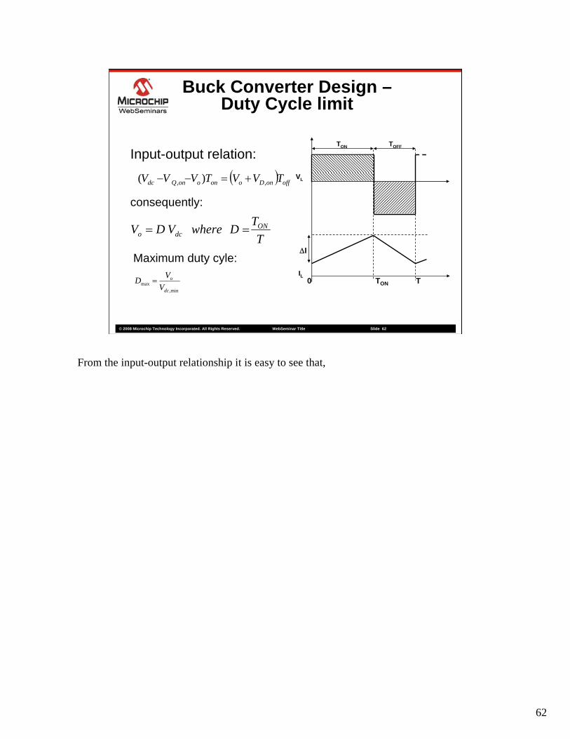
From the input-output relationship it is easy to see that,
63
© 2008 Microchip Technology Incorporated. All Rights Reserved. WebSeminar Title Slide 63
Buck Converter Design –Duty Cycle limit
Input-output relation:
IILL
ΔI
VVLL( ) offonDoonoonQdc TVVTVVV ,, )( +=−−
TON TOFF
min,max
dc
o
VVD =
consequently:
Maximum duty cyle:T
TDwhereVDV ONdco ==
0 TON T
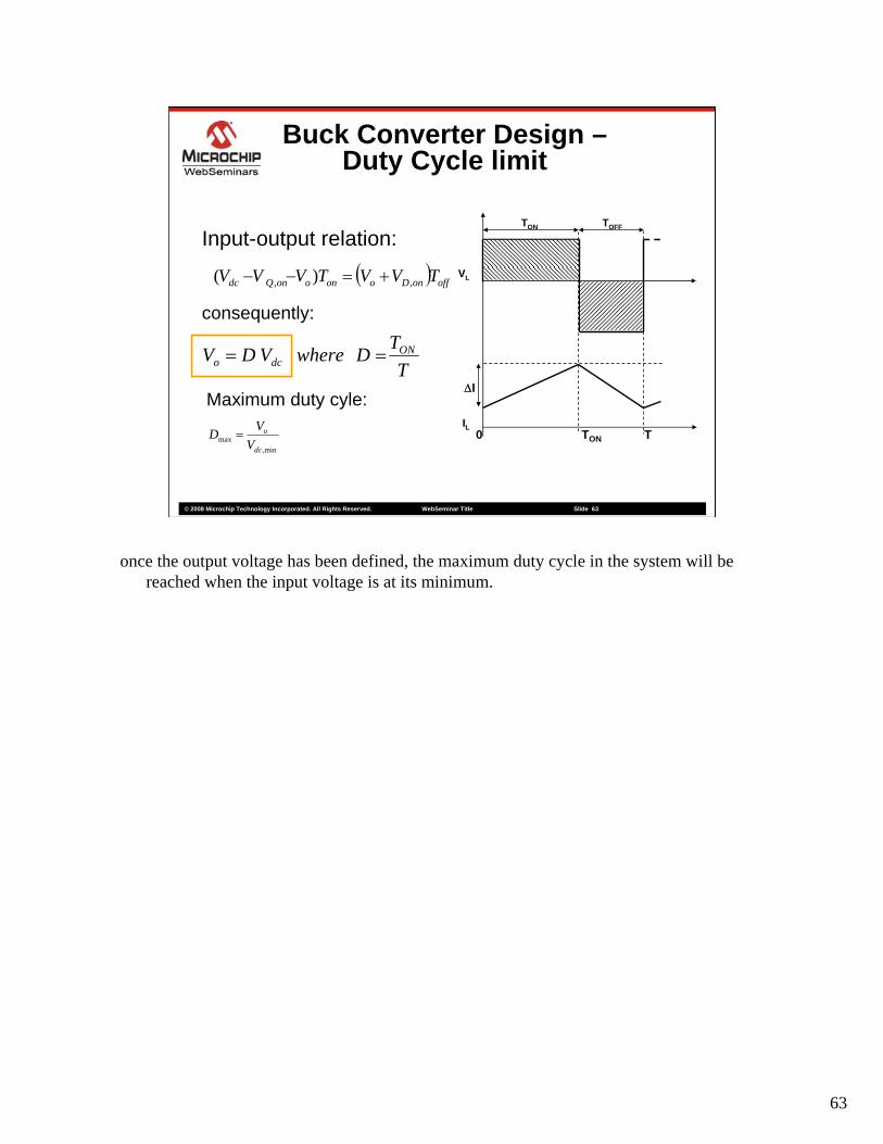
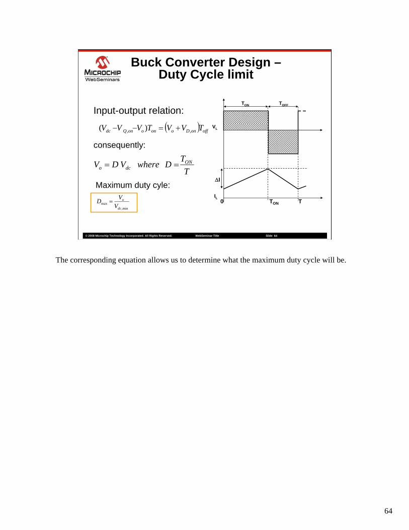
once the output voltage has been defined, the maximum duty cycle in the system will be reached when the input voltage is at its minimum.
64
© 2008 Microchip Technology Incorporated. All Rights Reserved. WebSeminar Title Slide 64
Buck Converter Design –Duty Cycle limit
Input-output relation:
IILL
ΔI
VVLL( ) offonDoonoonQdc TVVTVVV ,, )( +=−−
TON TOFF
min,max
dc
o
VVD =
consequently:
Maximum duty cyle:T
TDwhereVDV ONdco ==
0 TON T
The corresponding equation allows us to determine what the maximum duty cycle will be.
65
© 2008 Microchip Technology Incorporated. All Rights Reserved. WebSeminar Title Slide 65
Buck Converter Design –Inductor
( )on
onomdcnomavoavo T
LVV
II1
,,,min,, 2
1.0−
==
nomavoavo II ,,min,, 1.0=
( )nomavoPWMnomdc
oonomdc
IFVVVV
L,,,
,1
5 −=
Solving
RL
VO
D1
v1
C1
L1
Vdc
Q1vL
IILL
Io,av,nom
Io,av,min
10%10%
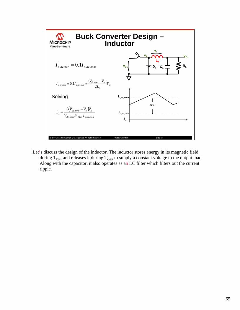
Let’s discuss the design of the inductor. The inductor stores energy in its magnetic field during TON, and releases it during TOFF to supply a constant voltage to the output load. Along with the capacitor, it also operates as an LC filter which filters out the current ripple.
66
© 2008 Microchip Technology Incorporated. All Rights Reserved. WebSeminar Title Slide 66
Buck Converter Design –Inductor
( )on
onomdcnomavoavo T
LVV
II1
,,,min,, 2
1.0−
==
nomavoavo II ,,min,, 1.0=
( )nomavoPWMnomdc
oonomdc
IFVVVV
L,,,
,1
5 −=
Solving
RL
VO
D1
v1
C1
L1
Vdc
Q1vL
IILL
Io,av,nom
Io,av,min
10%10%
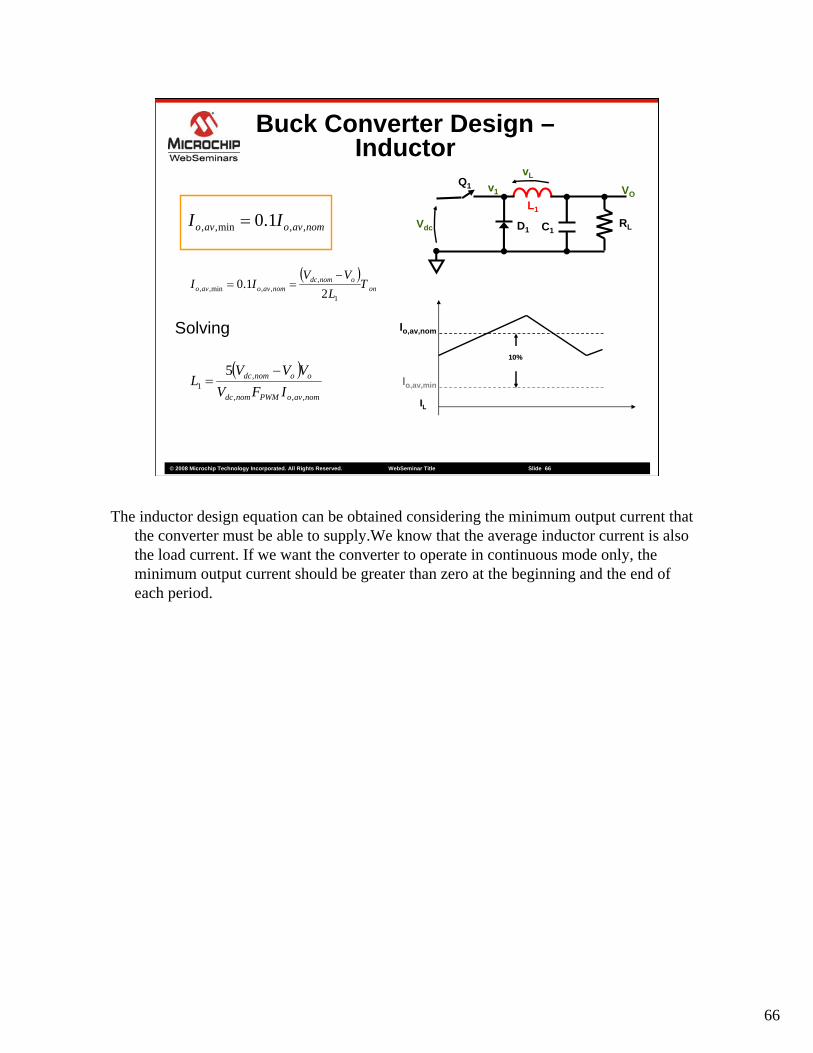
The inductor design equation can be obtained considering the minimum output current that the converter must be able to supply.We know that the average inductor current is also the load current. If we want the converter to operate in continuous mode only, the minimum output current should be greater than zero at the beginning and the end of each period.
67
© 2008 Microchip Technology Incorporated. All Rights Reserved. WebSeminar Title Slide 67
Buck Converter Design –Inductor
( )on
onomdcnomavoavo T
LVV
II1
,,,min,, 2
1.0−
==
nomavoavo II ,,min,, 1.0=
( )nomavoPWMnomdc
oonomdc
IFVVVV
L,,,
,1
5 −=
Solving
RL
VO
D1
v1
C1
L1
Vdc
Q1vL
IILL
Io,av,nom
Io,av,min
10%10%
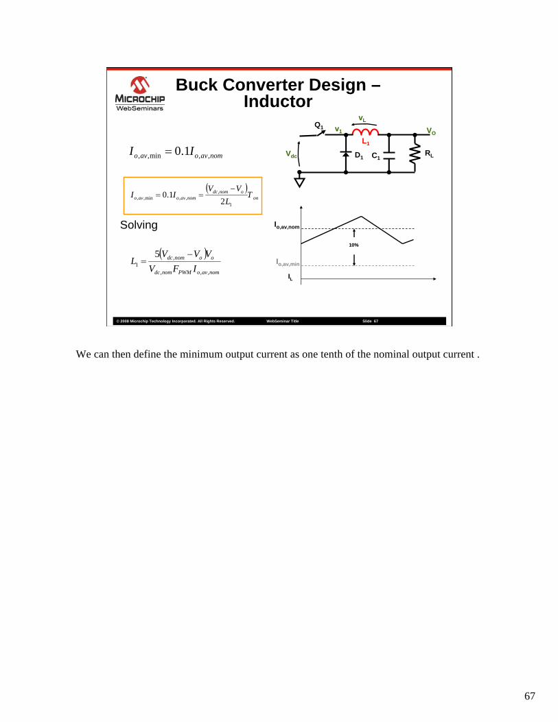
We can then define the minimum output current as one tenth of the nominal output current .
68
© 2008 Microchip Technology Incorporated. All Rights Reserved. WebSeminar Title Slide 68
Buck Converter Design –Inductor
( )on
onomdcnomavoavo T
LVV
II1
,,,min,, 2
1.0−
==
nomavoavo II ,,min,, 1.0=
( )nomavoPWMnomdc
oonomdc
IFVVVV
L,,,
,1
5 −=
Solving
RL
VO
D1
v1
C1
L1
Vdc
Q1vL
IILL
Io,av,nom
Io,av,min
10%10%
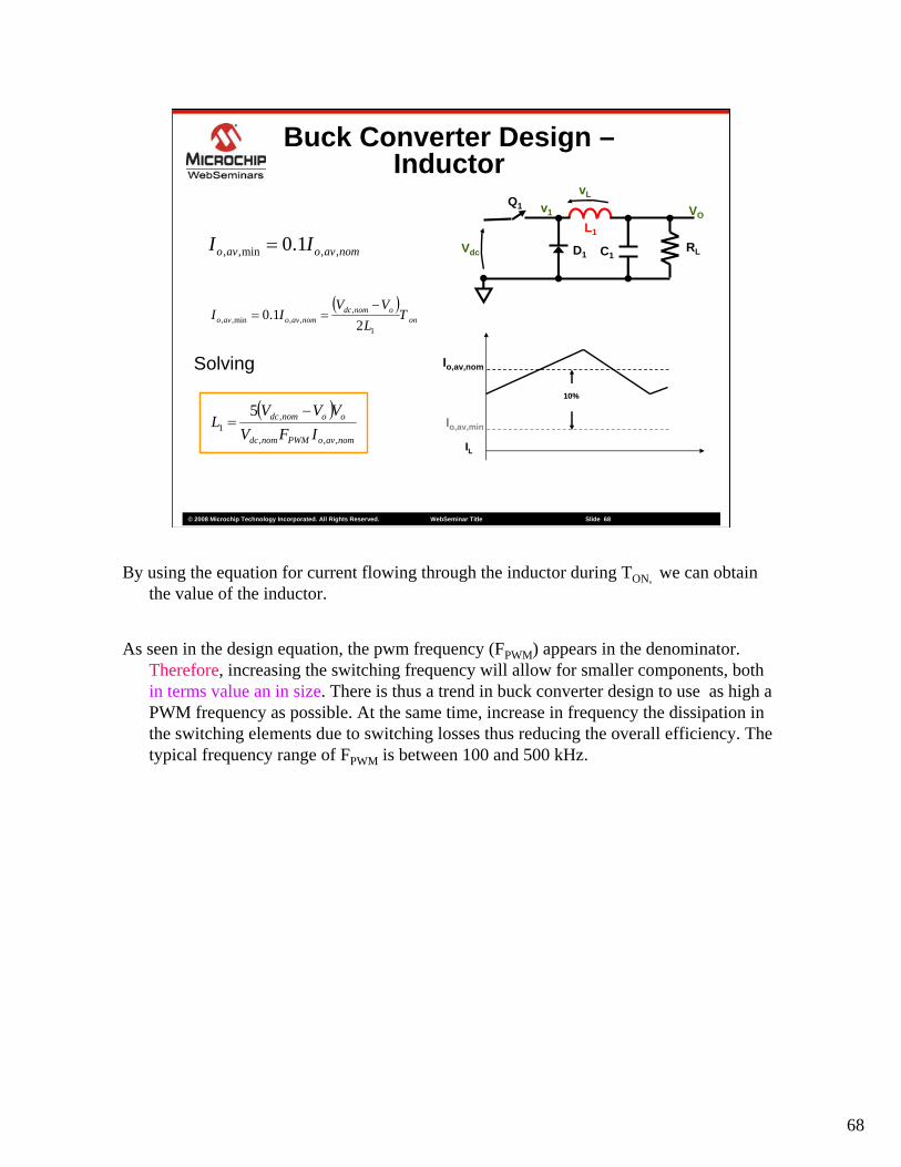
By using the equation for current flowing through the inductor during TON, we can obtain the value of the inductor.
As seen in the design equation, the pwm frequency (FPWM) appears in the denominator. Therefore, increasing the switching frequency will allow for smaller components, both in terms value an in size. There is thus a trend in buck converter design to use as high a PWM frequency as possible. At the same time, increase in frequency the dissipation in the switching elements due to switching losses thus reducing the overall efficiency. The typical frequency range of FPWM is between 100 and 500 kHz.
69
© 2008 Microchip Technology Incorporated. All Rights Reserved. WebSeminar Title Slide 69
Buck Converter Design –Output Capacitor
RL
VO
D1
v1
C1
L1
Vdc
Q1
vL
[ ]LESRtotalrPWM
L
IRVFDI
CΔ−Δ
Δ=
,0
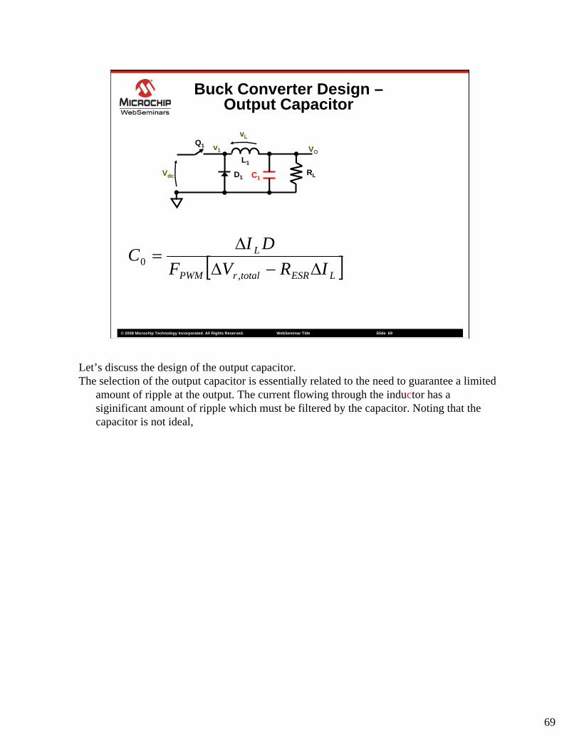
Let’s discuss the design of the output capacitor. The selection of the output capacitor is essentially related to the need to guarantee a limited
amount of ripple at the output. The current flowing through the inductor has a siginificant amount of ripple which must be filtered by the capacitor. Noting that the capacitor is not ideal,
70
© 2008 Microchip Technology Incorporated. All Rights Reserved. WebSeminar Title Slide 70
Buck Converter Design –Output Capacitor
RL
VO
D1
v1
C1
L1
Vdc
Q1
vL
[ ]LESRtotalrPWM
L
IRVFDI
CΔ−Δ
Δ=
,0
RRESRESR
LLESLESL
CC
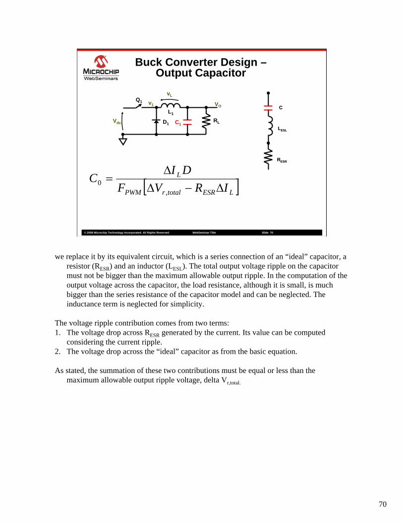
we replace it by its equivalent circuit, which is a series connection of an “ideal” capacitor, a resistor (RESR) and an inductor (LESL). The total output voltage ripple on the capacitor must not be bigger than the maximum allowable output ripple. In the computation of the output voltage across the capacitor, the load resistance, although it is small, is much bigger than the series resistance of the capacitor model and can be neglected. The inductance term is neglected for simplicity.
The voltage ripple contribution comes from two terms:1. The voltage drop across RESR generated by the current. Its value can be computed
considering the current ripple.2. The voltage drop across the “ideal” capacitor as from the basic equation.
As stated, the summation of these two contributions must be equal or less than the maximum allowable output ripple voltage, delta Vr,total.
71
© 2008 Microchip Technology Incorporated. All Rights Reserved. WebSeminar Title Slide 71
Buck Converter Design –Output Capacitor
RL
VO
D1
v1
C1
L1
Vdc
Q1
vL
[ ]LESRtotalrPWM
L
IRVFDI
CΔ−Δ
Δ=
,0
RRESRESR
LLESLESL
CC
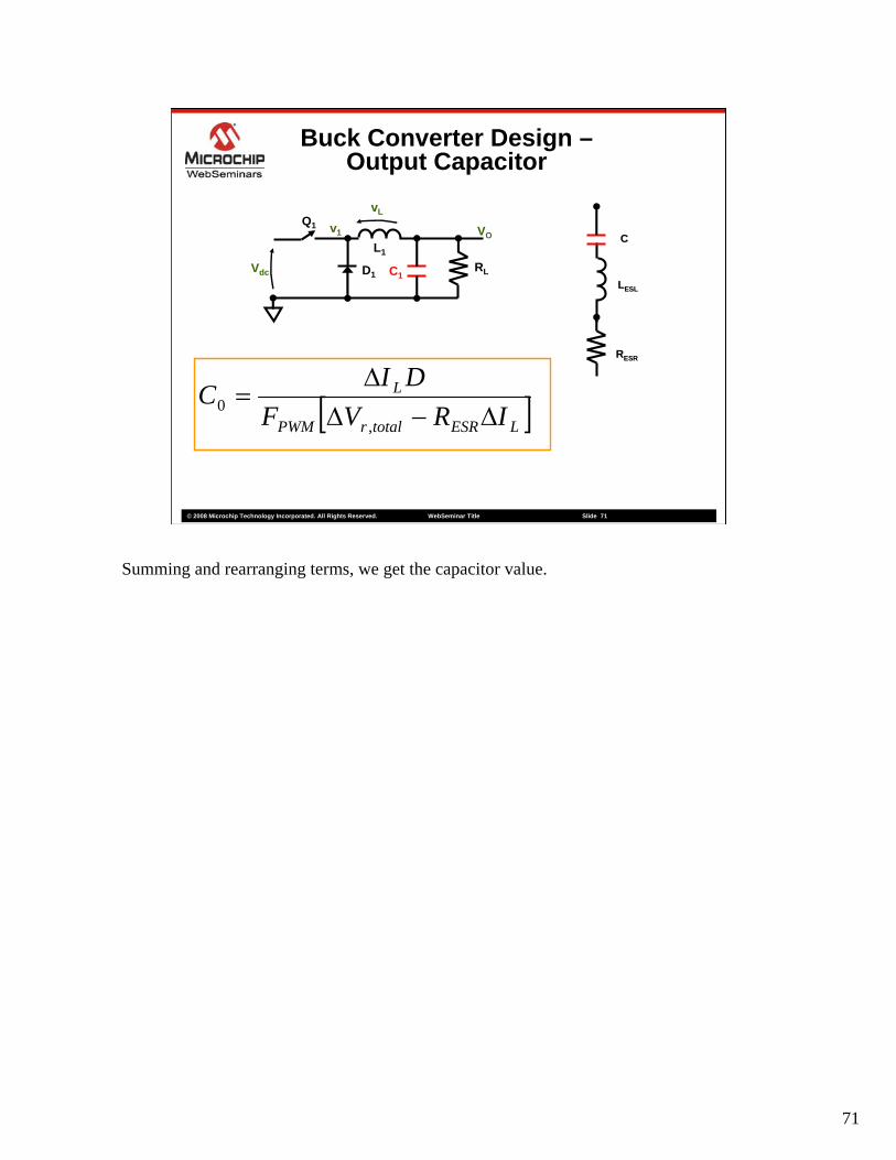
Summing and rearranging terms, we get the capacitor value.

72
© 2008 Microchip Technology Incorporated. All Rights Reserved. WebSeminar Title Slide 72
Buck Converter Design –Switch
Q1Q1cmdcmd
VVQQ
IIQQ
Io,av,nom
TON TOFF
onDdcQ VVV ,max,max, +=
DII nomavavQ ,,0, =
RL
VO
D1
v1
C1
L1
Vdc
Q1vL
Switch Q1 is usually a MOSFET device. The basic requirement is that the MOSFET must be able to withstand the maximum voltage and current that it will experience during the operation of the circuit.
As seen in the diagram, these values occur during TON and TOFF.
1. During TON the voltage across Q1 is near zero, the current is the same current flowing into the inductor and it has a linear up-slope behavior.
2. During TOFF the voltage across Q1 is at its maximum (close to Vdc) and the current is zero.
Consequently, the maximum voltage that the MOSFET must sustain is the maximum input voltage (Vdc,max), which is a design specification. It must comfortably handle the nominal output current (which is again a design specification).
73
© 2008 Microchip Technology Incorporated. All Rights Reserved. WebSeminar Title Slide 73
Buck Converter - Diode
Q1Q1cmdcmd
VVDD
IIDD
Io,av,nom
TON TOFF
onQdcD VVV ,max,max, +−=
Diode
)1(,,0, DII nomavavD −=
RL
VO
D1
v1
C1
L1
Vdc
Q1vL
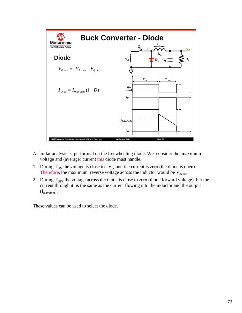
A similar analysis is performed on the freewheeling diode. We consider the maximum voltage and (average) current this diode must handle.
1. During TON the voltage is close to –Vdc and the current is zero (the diode is open). Therefore, the maximum reverse voltage across the inductor would be Vdc,ma
2. During TOFF the voltage across the diode is close to zero (diode forward voltage), but the current through it is the same as the current flowing into the inductor and the output (Io,av,nom).
These values can be used to select the diode.
74
© 2008 Microchip Technology Incorporated. All Rights Reserved. WebSeminar Title Slide 74
Buck Converter –Voltage mode Control
PWMGENERATOR
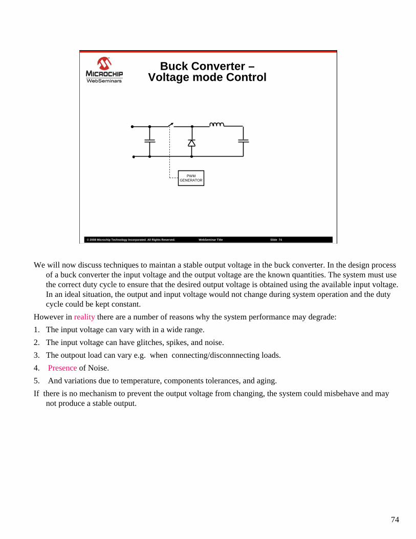
We will now discuss techniques to maintan a stable output voltage in the buck converter. In the design process of a buck converter the input voltage and the output voltage are the known quantities. The system must use the correct duty cycle to ensure that the desired output voltage is obtained using the available input voltage. In an ideal situation, the output and input voltage would not change during system operation and the duty cycle could be kept constant.
However in reality there are a number of reasons why the system performance may degrade:1. The input voltage can vary with in a wide range.2. The input voltage can have glitches, spikes, and noise.3. The outpout load can vary e.g. when connecting/disconnnecting loads.4. Presence of Noise.5. And variations due to temperature, components tolerances, and aging.If there is no mechanism to prevent the output voltage from changing, the system could misbehave and may
not produce a stable output.
75
© 2008 Microchip Technology Incorporated. All Rights Reserved. WebSeminar Title Slide 75
Buck Converter –Voltage mode Control
PWMGENERATOR VREF
EA
ERROR AMPLIFIERERROR AMPLIFIER
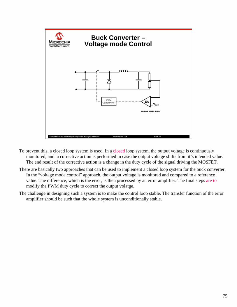
To prevent this, a closed loop system is used. In a closed loop system, the output voltage is continuously monitored, and a corrective action is performed in case the output voltage shifts from it’s intended value. The end result of the corrective action is a change in the duty cycle of the signal driving the MOSFET.
There are basically two approaches that can be used to implement a closed loop system for the buck converter. In the “voltage mode control” approach, the output voltage is monitored and compared to a reference value. The difference, which is the error, is then processed by an error amplifier. The final steps are tomodify the PWM duty cycle to correct the output volatge.
The challenge in designing such a system is to make the control loop stable. The transfer function of the error amplifier should be such that the whole system is unconditionally stable.
76
© 2008 Microchip Technology Incorporated. All Rights Reserved. WebSeminar Title Slide 76
Buck Converter –Current Mode Control Loop
VREFEA
PWMGENERATOR EAEA
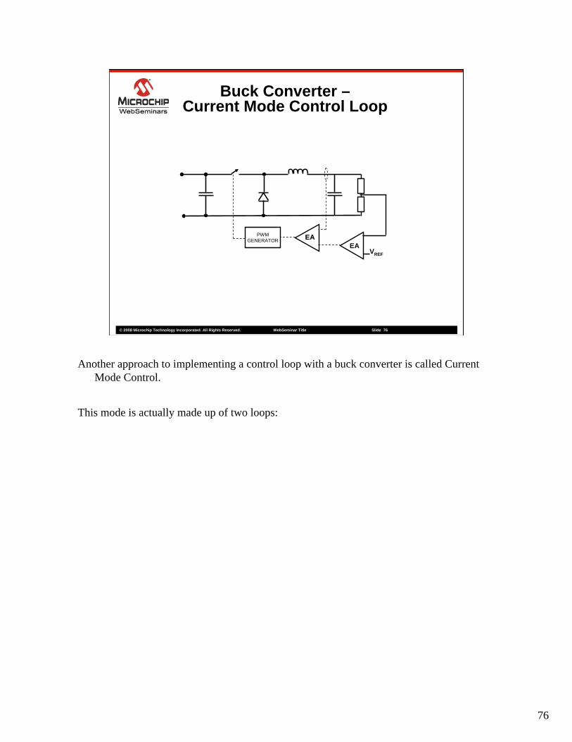
Another approach to implementing a control loop with a buck converter is called Current Mode Control.
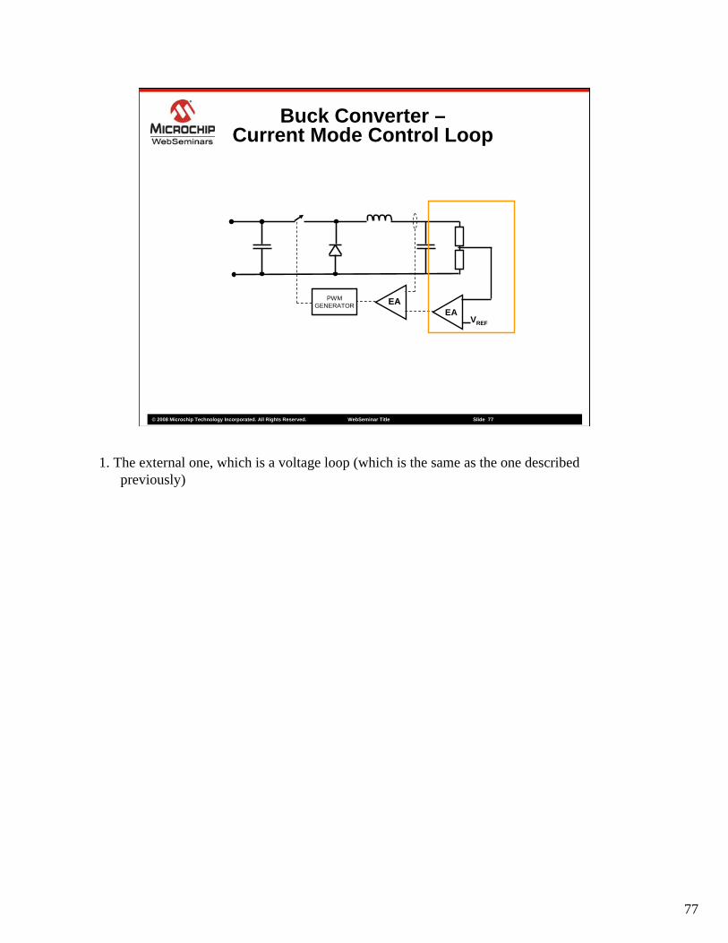
This mode is actually made up of two loops:
77
© 2008 Microchip Technology Incorporated. All Rights Reserved. WebSeminar Title Slide 77
Buck Converter –Current Mode Control Loop
VREFEA
PWMGENERATOR EAEA
1. The external one, which is a voltage loop (which is the same as the one described previously)
78
© 2008 Microchip Technology Incorporated. All Rights Reserved. WebSeminar Title Slide 78
Buck Converter –Current Mode Control Loop
VREFEA
PWMGENERATOR EAEA
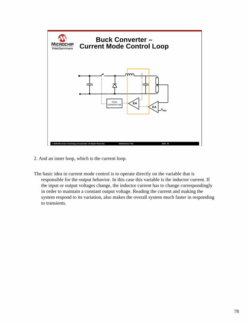
2. And an inner loop, which is the current loop.
The basic idea in current mode control is to operate directly on the variable that is responsible for the output behavior. In this case this variable is the inductor current. If the input or output voltages change, the inductor current has to change correspondingly in order to maintain a constant output voltage. Reading the current and making the system respond to its variation, also makes the overall system much faster in responding to transients.
79
© 2008 Microchip Technology Incorporated. All Rights Reserved. WebSeminar Title Slide 79
Buck Converter –SMPS dsPIC DSC
ACCUMULATOR
e(n)e(n)
e(ne(n--1)1)
e(ne(n--2)2)
KKAA
KKBB
KKCC
PWMduty cycle
register
BoundaryTests
ADC
SMPS dsPIC® DSC Device
(discarded)
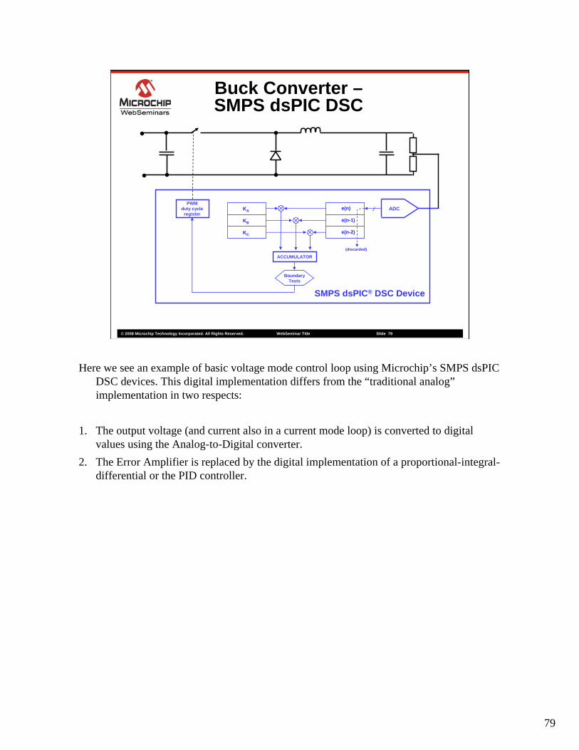
Here we see an example of basic voltage mode control loop using Microchip’s SMPS dsPIC DSC devices. This digital implementation differs from the “traditional analog”implementation in two respects:
1. The output voltage (and current also in a current mode loop) is converted to digital values using the Analog-to-Digital converter.
2. The Error Amplifier is replaced by the digital implementation of a proportional-integral-differential or the PID controller.
80
© 2008 Microchip Technology Incorporated. All Rights Reserved. WebSeminar Title Slide 80
Buck Converter –SMPS dsPIC DSC
ACCUMULATOR
e(n)e(n)
e(ne(n--1)1)
e(ne(n--2)2)
KKAA
KKBB
KKCC
PWMduty cycle
register
BoundaryTests
ADC
SMPS dsPIC® DSC Device
(discarded)
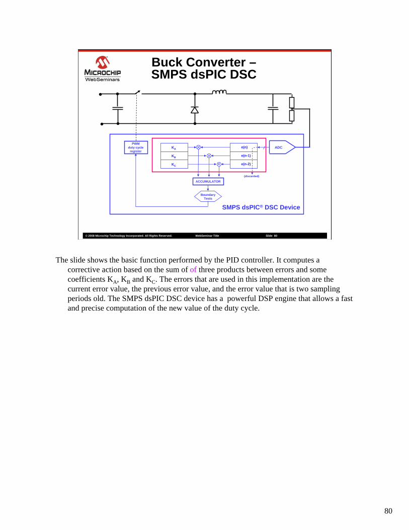
The slide shows the basic function performed by the PID controller. It computes a corrective action based on the sum of of three products between errors and some coefficients KA, KB and KC. The errors that are used in this implementation are the current error value, the previous error value, and the error value that is two sampling periods old. The SMPS dsPIC DSC device has a powerful DSP engine that allows a fast and precise computation of the new value of the duty cycle.
81
© 2008 Microchip Technology Incorporated. All Rights Reserved. WebSeminar Title Slide 81
Buck Converter –SMPS dsPIC DSC
ACCUMULATOR
e(n)e(n)
e(ne(n--1)1)
e(ne(n--2)2)
KKAA
KKBB
KKCC
PWMduty cycle
register
BoundaryTests
ADC
SMPS dsPIC® DSC Device
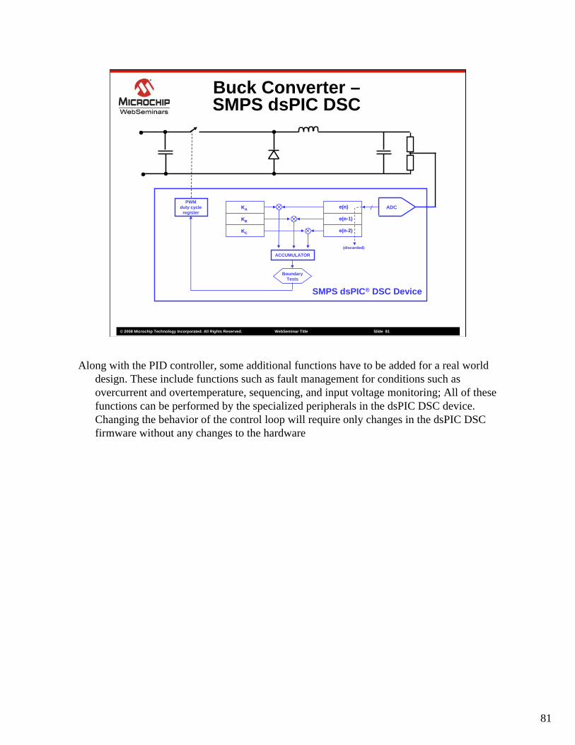
(discarded)
Along with the PID controller, some additional functions have to be added for a real world design. These include functions such as fault management for conditions such as overcurrent and overtemperature, sequencing, and input voltage monitoring; All of these functions can be performed by the specialized peripherals in the dsPIC DSC device. Changing the behavior of the control loop will require only changes in the dsPIC DSC firmware without any changes to the hardware
82
© 2008 Microchip Technology Incorporated. All Rights Reserved. WebSeminar Title Slide 82
Summary
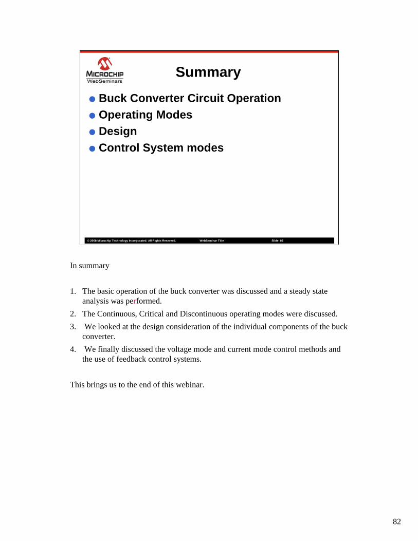
Buck Converter Circuit OperationOperating ModesDesignControl System modes
In summary
1. The basic operation of the buck converter was discussed and a steady state analysis was performed.
2. The Continuous, Critical and Discontinuous operating modes were discussed.3. We looked at the design consideration of the individual components of the buck
converter.4. We finally discussed the voltage mode and current mode control methods and
the use of feedback control systems.
This brings us to the end of this webinar.