Embed Size (px)
Citation preview
Switched-RC Beamforming Receivers in Advanced CMOS
Theory and Design
Michiel Soer
Switched-RC Beamforming
Receivers in Advanced CMOS
Theory and Design
Michiel Soer
Samenstelling promotiecommissie:
Voorzitter en secretaris:
Prof.dr.ir. A.J. Mouthaan Universiteit Twente
Promotor:
Prof.dr.ir. F.E. van Vliet Universiteit Twente
Assistent-promotor:
Dr.ing. E.A.M. Klumperink Universiteit Twente
Leden:
Prof.dr.ir. B. Nauta Universiteit Twente
Prof.ir. A.J.M. van Tuijl Universiteit Twente
Prof.dr.ir. D. Schreurs Katholieke Universiteit Leuven
Prof.dr. J.R. Long Technische Universiteit Delft
Referent:
Dr. A. Cathelin STMicroelectronics
This research was financially supported by the
Dutch Technology Foundation STW (07620).
Centre for Telematics and Information Technology
P.O. Box 217, 7500 AE
Enschede, The Netherlands
Centre for Array Technology.
ISSN: 1381-3617 (CTIT Ph.D. Thesis Series No. 12-233)
ISBN: 978-90-365-3436-9
DOI: http://dx.doi.org/10.3990/1.9789036534369
Copyright c© 2012 by Michiel Soer, Enschede, The Netherlands
All rights reserved.
Typeset with LATEX.
This thesis was printed by Gildeprint Drukkerijen, The Netherlands.
Switched-RC Beamforming
Receivers in Advanced CMOS
Theory and Design
Proefschrift
ter verkrijging van
de graad van doctor aan de Universiteit Twente,
op gezag van de rector magnificus,
prof. dr. H. Brinksma,
volgens besluit van het College voor Promoties
in het openbaar te verdedigen
op donderdag 22 november 2012 om 16:45 uur
door
Michiel Cornelius Marinus Soer
geboren op 19 juli 1984
te Schoonhoven

Dit proefschrift is goedgekeurd door:
de promotor prof.dr.ir. F.E van Vliet
de assistent-promotor dr.ing. E.A.M. Klumperink

Samenvatting
In consumentenelektronica wordt de daadwerkelijke draadloze verbinding opgebouwd
door analoge radio zenders en ontvangers. Deze radio’s zijn voornamelijk omni-
directioneel, zodanig dat zenders hun energy in alle richtingen verspreiden en zen-
ders gevoelig zijn voor signalen die uit elke richting kunnen komen. Vanwege deze
eigenschappen wordt met de toenemende hoeveelheid aan draadloze verbindingen de
interferentie tussen apparaten en diensten steeds problematischer. Voor het sturen
van en luisteren naar radio signalen uit specifieke richtingen is het noodzakelijk om
meerdere antennes aan de radio’s te verbinden en precieze tijdvertragingen tussen deze
antennes aan te brengen. De resulterende ”bundelvorming”kan begrepen worden als
een soort van ruimtelijk filter.
De implementatie van een dergelijk systeem in consumentenelektronica vereist dat
circuits met tijdsvertraging en/of fasedraaing worden toegevoegd aan de bestaande
radio architecturen. Deze circuits zijn lastig te fabriceren in de geıntegreerde circuit
(IC) technologie die gebruikt wordt voor consumentenapparaten. Daarom onderzoekt
dit proefschrift de uitvoering van bundelvormende ontvangers in geavanceerd comple-
mentary metal oxide semiconductor (CMOS) IC technologie.
Het bundelvormingsmechanisme is gedefinieerd in de vorm van antenne vertragin-
gen in het radiofrequentie (RF) domein. Analyse van de bundelvormingseigenschap-
pen laat zien dat voor smalbandige systemen de fasedraaing verplaats kan worden tot
na de frequentietranslatie, naar het tussenfrequentie (IF) domein. De translatie kan
meteen de 90-graden-uit-fase signalen genereren die nodig zijn voor een fasedraaier
van het vector-modulator type. Bovendien vermindert de vertaling naar het IF do-
mein de benodigde bandbreedte in de fasedraaier.
Een nadeel van IF bundelvorming bestaat eruit dat de mixers en versterkers in
het eerste stuk van de ontvanger bloot staan aan de ongefilterde verstoorders, zodat
de vervorming die gegenereerd wordt door deze componenten laag gehouden moet
worden. Het is bekend dat een lage vervorming in CMOS technologie bereikt kan
worden door passieve schakelende circuits, bijvoorbeeld door geschakelde-weerstand-
capaciteit mixers en spanningssamplers. Met een uitvoerige analyse wordt aangetoond
dat het basis bouwblok van deze circuits bestaat uit een enkel geschakelde-weerstand-
i
Samenvatting
capaciteit stroomlus. Bovendien wordt er geconcludeerd dat de overdrachtsfunctie
en ruisbijdrage van deze lus afhangen van de verhouding tussen de RC tijdconstante
en de tijd dat de schakelaar aan staat. Twee duidelijke werkingsgebieden worden
aangeduid, waarvan de eerste lage ruis eigenschappen heeft voor mixer toepassingen
en de tweede hoge bandbreedtes aanbiedt voor sampler toepassingen.
De goede vervormingseigenschappen van deze circuits worden optimaal benut, in-
dien de mixer-eerst architectuur wordt gebruikt, waarin de frequentietranslatie met
een geschakelde-RC mixer wordt uitgevoerd voordat er versterking plaatsvind. Door-
dat de versterking plaatsvindt in het IF domein, is het mogelijk om feedback toe te
passen teneinde de vervorming te verlagen. Deze technieken zijn toegepast in een
65-nm CMOS ontvanger IC, met een derde-orde interceptie punt (IIP3) van 11 dBm
en een ruisgetal (NF) van 6.5 dB. De RF frequentieband is kiesbaar tussen 200 MHz
en 2.0 GHz, hetgeen mogelijk wordt gemaakt door de van nature breedbandige mixer.
Vervolgens is het ontwerp van de vector-modulator fasedraaier aan de beurt, waar-
voor het nodig is om sinus en cosinus weging toe te passen op de 90-graden-uit-fase
signalen uit de mixer. Een goede benadering voor deze weging kan worden verkregen
door een circuit met ladingsherverdeling en geschakelde capaciteiten toe te passen.
Omdat de resulterende fasedraaing afhankelijk is van de verhoudingen tussen capaci-
teiten, is deze uiterst nauwkeurig gedefinieerd in een CMOS proces. De implementatie
van een 4-element 1.0-tot-4.0 GHz geıntegreerde ontvanger in 65-nm CMOS laat zien
dat de 5-bit fasedraaiers een root-mean-square (RMS) fasefout halen van slechts 1.4
graden, met een RMS versterkingsfout van 0.4 dB. Bovendien wordt de extra 3-bit
amplitudecontrole van de vector modulators gebruikt in een demonstratie van het
onderdrukken van verstoorders met meer dan 20 dB door middel van een bundelvor-
mingsalgoritme. Echter, het blijkt uit simulaties dat de vervorming (-1 dBm IIP3
binnen de band) gelimiteerd is door de actieve trappen in de bundelvormer.
Vandaar dat de overgang naar een compleet passieve bundelvormer gewenst is.
Hiervoor zullen echter de koppelingen tussen de geschakelde-RC circuits in de mixer en
de fasedraaier gemodelleerd moeten worden. Deze koppelingen kunnen gezien worden
als een effectieve weerstandsbelasting en er wordt een techniek gepresenteerd waarmee
de lading benodigd voor de aanpassing van de ingangsimpedantie hergebruikt kan
worden voor de fasedraaier. Met deze technieken is een volledig passieve 4-element
1.5-tot-5.0 GHz bundelvormende ontvanger geımplementeerd in 65-nm CMOS, met
een IIP3 van 13 dBm binnen de frequentieband en een NF van 18 dB. Bovendien
werkt de mixer als een mee schuivend frequentiefilter aan de ingang, waardoor het
compressiepunt wordt verhoogd van 2 dBm binnen de band tot een zeer hoge 12 dBm
buiten de band. De resultaten tonen aan dat deze topologie voor een bundelvormer
in CMOS zeer bestendig is tegen sterke verstoorders.
ii
Abstract
In consumer electronic devices, analog radio transmitters and receivers provide the
wireless links between devices. These radios are mostly omni-directional, i.e. trans-
mitters send their energy in all directions and receivers listen to signals from all
directions. As a result, interference between devices and services is becoming an
increasing problem as more wireless connectivity is added. In order to steer radio sig-
nals toward their destination and to receive from a specific direction, it is necessary
to add multiple antennas to the radios and to control their precise relative delays.
The resulting beamforming can be understood to be a form of spatial filtering.
For the implementation of such a system in consumer electronics, it is required
to add additional time delay and/or phase shift circuits to the existing radio archi-
tectures. These circuits are challenging to fabricate in the integrated circuit (IC)
technology used for consumer devices. Therefore, this thesis investigates the imple-
mentation of beamforming receivers in advanced complementary metal oxide semi-
conductor (CMOS) IC technology.
The beamforming is defined in terms of the antenna delays in the radio frequency
(RF) domain. An analysis of the beamforming properties reveals that in a narrowband
system, the phase shift can be moved until after downconversion to the intermediate
frequency (IF) domain. The downconversion can then generate 90-degree-out-of-phase
signals, necessary for the operation of a vector-modulator type phase shifter. More-
over, the shift to the IF domain significantly reduces the required bandwidth of the
phase shifter implementation.
A disadvantage of IF beamforming is that the frontend mixers and amplifiers are
subject to the unfiltered interferers, requiring a high linearity for these components.
In CMOS technology, high linearity is achieved by passive switching circuits, such as
switched-RC mixers and voltage samplers. A rigorous analysis reveals that a switched-
resistor-capacitor current loop is the basic building block of these systems. It is also
concluded that the transfer function and noise contribution of this loop depend on
the ratio between the RC time constant and the switch-on time. Two distinctive
operating regions are identified, one with low noise properties for mixer applications,
and one with high bandwidth properties for sampling applications.
iii
Abstract
In order to take advantage of the good linearity properties of these circuits, the
mixer-first architecture is proposed. In this architecture, downconversion with an
inherently linear switched-RC mixing-region mixer takes place before amplification.
By postponing the amplification to the IF domain, feedback can be applied to increase
amplifier linearity. These concepts are demonstrated in a 65-nm CMOS receiver IC,
achieving an 11 dBm input-referred third-order intercept point (IIP3) and a 6.5 dB
noise figure (NF), which translates into 79 dB of spurious free dynamic range in 1
MHz bandwidth. Due to the wideband nature of the mixer, a tunable RF input band
of 200 MHz up to 2 GHz is achieved.
Next, the design of the IF domain vector-modulator phase shifter is considered,
in which it is required to apply sine and cosine weighting on the 90-degree-out-of-
phase signals from the mixer. It is shown that a good approximation of the weighting
can be achieved by a charge-redistribution switched-capacitor circuit. The resulting
phase shift is a function of capacitor ratios, which are very well defined in CMOS
processes. A 4-element 1.0-to-4.0 GHz integrated receiver is implemented in 65-nm
CMOS, including 5-bit phase shifters with a root-mean-square (RMS) phase error of
1.4 degrees and a RMS gain error of 0.4 dB. Using the additional 3-bit gain control of
the vector modulator, a beamforming infererence nulling algorithm is demonstrated
which is able to suppress interferers by more than 20 dB. In this design, simulations
indicate that the limiting factor in linearity (-1 dBm in-band IIP3) is formed by the
active stages in the beamforming network.
Therefore, the transition to a fully passive, switched-RC beamforming receiver is
desired. This requires the modeling of the coupling between the mixing-region mixer
and the sampling-region phase shifter. By defining an effective input resistance for
the two stages, its loading effects can be examined, and it is found that the charge
dissipation in the phase shifter can be used to implement input matching at the
mixer input. Using this design framework, a fully-passive 4-element 1.5-to-5.0 GHz
beamforming receiver is implemented in 65-nm CMOS, with an in-band IIP3 of 13
dBm and a NF of 18 dB. It is also found that intrinsic filtering at the mixer input
occurs, boosting the compression point from 2 dBm in-band to a very high 12 dBm
out-of-band, demonstrating the high resilience of this CMOS beamforming topology
to strong interferers.
iv

Contents
Samenvatting i
Abstract iii
1 Introduction 1
1.1 Wireless Communications . . . . . . . . . . . . . . . . . . . . . . . . . 1
1.2 CMOS Integrated Circuit Technology . . . . . . . . . . . . . . . . . . 2
1.3 Multi-Antenna Wireless Systems . . . . . . . . . . . . . . . . . . . . . 4
1.4 Motivation and Thesis Outline . . . . . . . . . . . . . . . . . . . . . . 7
2 Phased-Array Downconverting Receivers 9
2.1 Linear Array Theory . . . . . . . . . . . . . . . . . . . . . . . . . . . . 9
2.1.1 Beam Steering . . . . . . . . . . . . . . . . . . . . . . . . . . . 10
2.1.2 Narrowband Phase Shifter Approximation . . . . . . . . . . . . 13
2.1.3 Directivity . . . . . . . . . . . . . . . . . . . . . . . . . . . . . 14
2.1.4 Amplitude Tapering . . . . . . . . . . . . . . . . . . . . . . . . 17
2.1.5 Null Steering . . . . . . . . . . . . . . . . . . . . . . . . . . . . 18
2.1.6 Random Errors . . . . . . . . . . . . . . . . . . . . . . . . . . . 20
2.1.7 Phase Quantization Errors . . . . . . . . . . . . . . . . . . . . 22
2.1.8 Amplitude Quantization Errors . . . . . . . . . . . . . . . . . . 23
2.2 Frequency Translation and Beamforming . . . . . . . . . . . . . . . . . 24
2.2.1 Effects of Phase Shift and Time Delay . . . . . . . . . . . . . . 24
2.2.2 Transformations . . . . . . . . . . . . . . . . . . . . . . . . . . 27
2.3 RF System Design Aspects . . . . . . . . . . . . . . . . . . . . . . . . 30
2.3.1 Bandwidth and Architecture . . . . . . . . . . . . . . . . . . . 31
2.3.2 Linearity and Noise . . . . . . . . . . . . . . . . . . . . . . . . 32
2.4 Conclusions . . . . . . . . . . . . . . . . . . . . . . . . . . . . . . . . . 33
v
Contents
3 Highly-Linear Mixer-First Receiver Front-Ends 34
3.1 Switched-RC Mixers and Samplers . . . . . . . . . . . . . . . . . . . . 35
3.1.1 LPTV Systems . . . . . . . . . . . . . . . . . . . . . . . . . . . 36
3.1.2 Decomposition into Polyphase Kernels . . . . . . . . . . . . . . 38
3.1.3 Kernel Analysis . . . . . . . . . . . . . . . . . . . . . . . . . . . 40
3.1.4 Polyphase Multi-path Analysis . . . . . . . . . . . . . . . . . . 44
3.1.5 Noise . . . . . . . . . . . . . . . . . . . . . . . . . . . . . . . . 46
3.1.6 Application to Low-Noise Passive Mixers . . . . . . . . . . . . 50
3.2 Implementation in 65-nm CMOS . . . . . . . . . . . . . . . . . . . . . 52
3.2.1 Mixer and Feedback Amplifier . . . . . . . . . . . . . . . . . . 52
3.2.2 Clock Generation . . . . . . . . . . . . . . . . . . . . . . . . . . 54
3.2.3 Measurements . . . . . . . . . . . . . . . . . . . . . . . . . . . 56
3.3 Conclusions . . . . . . . . . . . . . . . . . . . . . . . . . . . . . . . . . 57
4 Approximate-Sine Vector Modulator Beamforming 58
4.1 Switched-Capacitor Phase Shifter . . . . . . . . . . . . . . . . . . . . . 58
4.1.1 Vector Modulator Principle . . . . . . . . . . . . . . . . . . . . 59
4.1.2 Sine/Cosine Approximation for Non-Uniform Weighting . . . . 60
4.1.3 Amplitude Control for Null Steering . . . . . . . . . . . . . . . 64
4.2 Implementation in 65-nm CMOS . . . . . . . . . . . . . . . . . . . . . 65
4.2.1 Mixer . . . . . . . . . . . . . . . . . . . . . . . . . . . . . . . . 66
4.2.2 Vector Modulator . . . . . . . . . . . . . . . . . . . . . . . . . 67
4.2.3 Element Summing . . . . . . . . . . . . . . . . . . . . . . . . . 68
4.2.4 Clock generation . . . . . . . . . . . . . . . . . . . . . . . . . . 69
4.2.5 Measurements . . . . . . . . . . . . . . . . . . . . . . . . . . . 70
4.3 Conclusions . . . . . . . . . . . . . . . . . . . . . . . . . . . . . . . . . 74
5 All-Passive Switched-Capacitor Phased Array 75
5.1 Coupling of Switched-RC Loops . . . . . . . . . . . . . . . . . . . . . . 76
5.1.1 Mixing Region Loops . . . . . . . . . . . . . . . . . . . . . . . 78
5.1.2 Input-Matched Passive Mixer . . . . . . . . . . . . . . . . . . . 79
5.1.3 Sampling Region Loops and Resistor Simulation . . . . . . . . 82
5.1.4 Phase Shifting . . . . . . . . . . . . . . . . . . . . . . . . . . . 83
5.1.5 Element Summing . . . . . . . . . . . . . . . . . . . . . . . . . 86
5.2 Implementation in 65-nm CMOS . . . . . . . . . . . . . . . . . . . . . 87
5.2.1 Mixer . . . . . . . . . . . . . . . . . . . . . . . . . . . . . . . . 88
5.2.2 Phase Shifter Slice . . . . . . . . . . . . . . . . . . . . . . . . . 89
5.2.3 Conversion Loss and Noise Figure . . . . . . . . . . . . . . . . 90
5.2.4 Clock Generation . . . . . . . . . . . . . . . . . . . . . . . . . . 91
5.2.5 Measurements . . . . . . . . . . . . . . . . . . . . . . . . . . . 92
vi

Contents
5.3 Conclusions . . . . . . . . . . . . . . . . . . . . . . . . . . . . . . . . . 96
6 Conclusions 98
6.1 Summary and Conclusions . . . . . . . . . . . . . . . . . . . . . . . . . 98
6.2 Original Contributions . . . . . . . . . . . . . . . . . . . . . . . . . . . 99
6.3 Future Work . . . . . . . . . . . . . . . . . . . . . . . . . . . . . . . . 100
A Switched-RC Kernel Analysis 102
A.1 LPTV Calculation Method . . . . . . . . . . . . . . . . . . . . . . . . 102
A.2 SE and DI Kernel Calculation . . . . . . . . . . . . . . . . . . . . . . . 105
A.3 Derivation of Kernel Approximations . . . . . . . . . . . . . . . . . . . 108
A.3.1 Mixing Region . . . . . . . . . . . . . . . . . . . . . . . . . . . 108
A.3.2 Sampling Region . . . . . . . . . . . . . . . . . . . . . . . . . . 110
A.4 Derivation of Kernel Noise . . . . . . . . . . . . . . . . . . . . . . . . . 110
A.4.1 Mixing Region . . . . . . . . . . . . . . . . . . . . . . . . . . . 111
A.4.2 Sampling Region . . . . . . . . . . . . . . . . . . . . . . . . . . 111
B Integrals and Sums 113
Dankwoord 115
Bibliography 117
List of Publications 123
List of Abbreviations 125
vii

Chapter 1
Introduction
1.1 Wireless Communications
Imagine throwing a rock in a pond. The impact of the rock will form waves on the
surface of the water, traveling away from the location of the splash in circles. Next,
consider a fisherman who is fishing somewhere further along the shore of the pond.
His floater will oscillate along with the water waves, and he can deduce from this
observation that something has disturbed the water some distance away. He can
draw two important conclusions.
First, it is apparent that the impact of the waves on the receiver becomes weaker as
the distance to the source increases. The energy of the wave is spread across a larger
circumference, making it harder to detect the wave. Secondly, from the bobbling of
the floater, he cannot tell where the source is located.
Of course, the surface of the water needs to be calm for the fisherman in order to
detect the ripples caused by the rock. When a storm is going on, the waves formed
by the wind are so large that the smaller ripples are completely obscured. Moreover,
if multiple persons are throwing rocks in the pond, the ripples will interfere and make
it hard for him to distinguish between them.
Not all water waves behave this way, as can be observed when one sits next to the
water front of a lake. Sometimes, a bow wave can be seen coming from no apparent
source, striking the water front and reflecting back on the lake. Obviously, it has
traveled quite a long distance, as there is no boat in sight and as the wave speeds
away again, it does not seem to lose significant amplitude. It seems that the boat
causing the bow wave was able to direct its energies towards a specific propagation
direction, instead of the circular wave generated by throwing a rock into the water.
1
1. Introduction
Personal wireless communication devices have secured a firm position in our lives.
Whether you are making a phone call to relatives, browsing the web on your laptop
through a wireless network (WLAN) or checking the train departure times on your
smart phone through a 4G LTE connection, something is happening inside these
devices to establish a connection over large distances.
The primary physical effect that is being exploited is the propagation of waves
in the electromagnetic (EM) field. This is analogous to throwing a rock in a pond,
where the role of rock and floater is taken up by specially formed pieces of metal,
called antenna. As water waves will become weaker with increasing distance, so do
EM waves become increasingly harder to detect, putting a maximum range beyond
which no reception is possible.
Moreover, the receiver has no direct information about the location of the trans-
mitter. When there are multiple transmitters, their waves will interfere and make it
harder for the receiver to detect the desired signal.
The source of the range limitation and interference issues can be found in the omni-
directional (isotropic) characteristics of the antenna in the receiver and transmitter.
As the transmit antenna sends its signal in all directions and the receiver listens to
all directions simultaneously, a lot of energy is wasted. If the transmitter and receiver
could be made more directional, the range would increase and the interference between
transmissions would decrease.
In the pond analogy, it was noted that not all water waves are circular, but that
bow waves move in a specific direction. The same mechanism can be achieved with
electromagnetic waves by transmitting the signal with multiple antennas at the same
time. The EM energy can be steered to specific directions, increasing its effectiveness.
Moreover, the receiver can also be outfitted with multiple antennas in order to listen
to a specific direction, thereby increasing its sensitivity.
The use of multiple-antenna systems is now entering the consumer market in
the latest wireless standards. This step promises to increase data rates, reduce co-
existence interference and in general improve the quality of service for the consumer.
In this thesis, the use of these multi-antenna systems in modern wireless consumer
electronics is investigated.
1.2 CMOS Integrated Circuit Technology
Aside from the physical principles of wireless systems, there are the electrical devices
themselves to consider. It requires a lot of signal processing to generate suitable signals
for transmission through the EM medium, as well as for amplifying and decoding the
resulting received signal. Moreover, there is all the digital logic needed to interact with
the user and provide a rich user experience. The combination of enormous processing
2
1. Introduction
130 90 65 45 320
100
200
300
400
Feature size [nm]
Ma
x. tr
ansitio
n fre
quen
cy [G
Hz]
2001 2004
2007
2009
2011
(a)
Inductor
Capacitor
RF
Transistor
Logic
Microwave
Component TypeCompound
Technology
CMOS
Technology
(b)
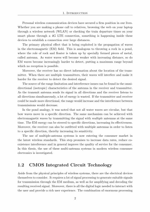
Figure 1.1: (a) International Technology Roadmap for Semiconductors year of intro-
duction and maximum transition frequency of 130-nm towards 32-nm CMOS [3] and
(b) compatibility of component types with compound and CMOS technology.
power in a minuscule form factor has only been possible with the invention of the
integrated circuit (IC) by Jack Kilby in 1959 [1].
Instead of assembling electrical circuits component-by-component, the circuits in
ICs are constructed all at once, drastically reducing the price per component to fan-
tastically low level. The basic production procedure involves growing patterned layers
on top of a semiconductor substrate, thereby forming the components as well as their
interconnection. The finished IC is a small silvery slab the size and thickness of a
fingernail, but packing up to several billion components [2].
The inclusion of more and more functionality on a single IC (or chip) is known
as integration. Two major substrate types are in use for the fabrication of ICs, with
different trade-offs in integration and performance. First of all, there are the technolo-
gies using a compound between III and V materials in the periodic table. Examples
are Gallium-Arsenide (GaAs), Indium-Phosphide (InP) and Gallium-Nitride (GaN).
These offer the best performance, at the expense of integration and at a rather high
cost, and therefore find uses mostly in the defense and scientific sector.
On the other hand, there are the technologies based on silicon, a IV material, lit-
erally as abundant as sand (which is silicon dioxide). Aside from Silicon-Germanium
(SiGe), a cheaper alternative for the compound materials, there is the highly special-
ized silicon complementary metal oxide semiconductor (CMOS) technology. CMOS
is the main driver behind the consumer market, as it is very cheap to produce in mass
volumes and can achieve the highest integration, at the expense of performance.
CMOS is first and foremost developed for a high integration of digital electronics,
like processors and memories. Scaling is the key word here [4], the minimum compo-
3
1. Introduction
nent size (called feature size) steadily decreases from year to year, as is illustrated in
Fig. 1.1a. Hence, a doubling of the integrated functionality on the same chip area
for every two years is achieved. This is perceived by the consumer as an increase in
storage capacity and computing power that is available in electronic products every
year.
But, wireless transmitters and receivers are analog circuits and follow different
scaling rules than digital circuits. The decrease in transistor dimensions that is so
beneficial for digital integration has the effect of higher transition frequencies fTfor analog transconductor circuits. This transition frequency is a measure for the
maximum frequency for which meaningful amplification can be reached, indicating
that newer nodes can process higher frequency signals.
The improved switching speeds in advanced CMOS open up new communication
bands which where only reachable with compound technologies before. Costs for mass
produced products can be lowered by moving to CMOS, opening up these bands for
the broad public.
For the circuit designer, moving circuits from compound technologies to CMOS
can be challenging. Fig. 1.1b indicates the compatibility of components types with
the two technology families. Where as in compound technology the use of microwave
structures and inductors is beneficial for high frequency circuits, in CMOS these
components are more difficult to integrate. On the other hand, the performance of
switched circuits, derived from digital logic, in CMOS is increasing. It is up to the
circuit designer to develop circuits utilizing the components that scale best in newer
technologies.
1.3 Multi-Antenna Wireless Systems
As was sketched in the pond analogy, there is an advantage in expanding our wireless
systems to use multiple antennas. Instead of exciting and probing the electromagnetic
field in a singular point location1, extra degrees of freedom are created by placing
multiple point source some distance (in the order of the carrier wavelength) apart.
The techniques involving multiple antennas are referred to as multiple-input-multiple-
output (MIMO) systems and come in several varieties.
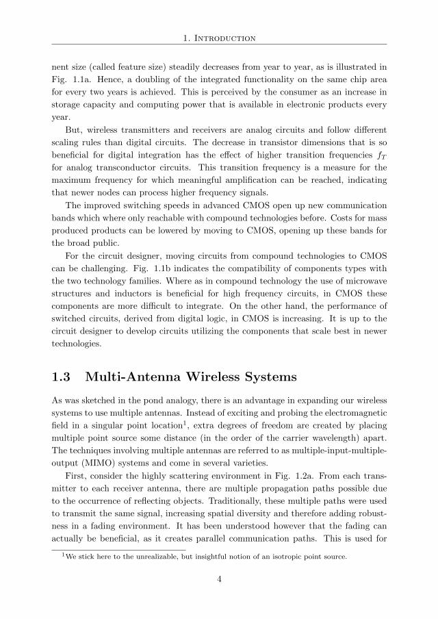
First, consider the highly scattering environment in Fig. 1.2a. From each trans-
mitter to each receiver antenna, there are multiple propagation paths possible due
to the occurrence of reflecting objects. Traditionally, these multiple paths were used
to transmit the same signal, increasing spatial diversity and therefore adding robust-
ness in a fading environment. It has been understood however that the fading can
actually be beneficial, as it creates parallel communication paths. This is used for
1We stick here to the unrealizable, but insightful notion of an isotropic point source.
4
1. Introduction
TX RX
(a)
TX RX
(b)
Figure 1.2: MIMO systems employing (a) spatial multiplexing and (b) beamforming.
spatial multiplexing, where multiple data streams are transmitted over orthogonal
transmit-receive paths [5], thereby increasing the capacity of the channel.
In a low scattering (line-of-sight) environment, Fig. 1.2b, the advantages of spatial
multiplexing are less as there is a lower orthogonality between receiver and transmitter
antenna pairs. Here, the high correlation between propagation paths can be used to
direct EM energy into specific directions. This process is known as beamforming, as
the signals are formed into a beam pointed at the receivers. The overall sensitivity
of the system is increased and the receiver becomes less sensitive to interferers with
a different angular position than the transmitter, as it is listening from a specific
direction.
The support for MIMO systems in consumer electronics has started only recently.
For WLAN, the IEEE 802.11n amendment defines transmit beamforming [6]. In
cellular systems, LTE release 9 defines several MIMO modes, including spatial mul-
tiplexing, downlink transmitter beamforming and a combination of the two [7]. Note
that these standards support full transmitter-receiver spatial multiplexing, but only
partial (transmitter) beamforming. From the receiver side, applying beamforming
has the potential to boost sensitivity and reject interferers [8].
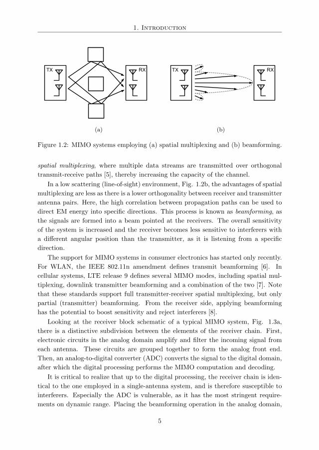
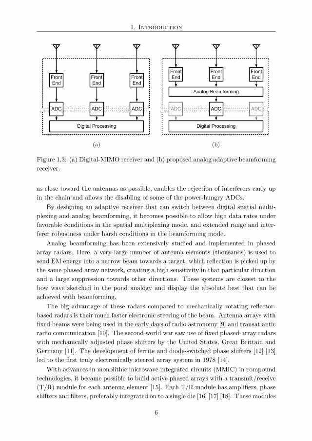
Looking at the receiver block schematic of a typical MIMO system, Fig. 1.3a,
there is a distinctive subdivision between the elements of the receiver chain. First,
electronic circuits in the analog domain amplify and filter the incoming signal from
each antenna. These circuits are grouped together to form the analog front end.
Then, an analog-to-digital converter (ADC) converts the signal to the digital domain,
after which the digital processing performs the MIMO computation and decoding.
It is critical to realize that up to the digital processing, the receiver chain is iden-
tical to the one employed in a single-antenna system, and is therefore susceptible to
interferers. Especially the ADC is vulnerable, as it has the most stringent require-
ments on dynamic range. Placing the beamforming operation in the analog domain,
5
1. Introduction
Front
End
Front
End
Front
End
ADC
Digital Processing
ADCADC
(a)
Front
End
Front
End
Front
End
ADC
Digital Processing
Analog Beamforming
ADCADC
(b)
Figure 1.3: (a) Digital-MIMO receiver and (b) proposed analog adaptive beamforming
receiver.
as close toward the antennas as possible, enables the rejection of interferers early up
in the chain and allows the disabling of some of the power-hungry ADCs.
By designing an adaptive receiver that can switch between digital spatial multi-
plexing and analog beamforming, it becomes possible to allow high data rates under
favorable conditions in the spatial multiplexing mode, and extended range and inter-
ferer robustness under harsh conditions in the beamforming mode.
Analog beamforming has been extensively studied and implemented in phased
array radars. Here, a very large number of antenna elements (thousands) is used to
send EM energy into a narrow beam towards a target, which reflection is picked up by
the same phased array network, creating a high sensitivity in that particular direction
and a large suppression towards other directions. These systems are closest to the
bow wave sketched in the pond analogy and display the absolute best that can be
achieved with beamforming.
The big advantage of these radars compared to mechanically rotating reflector-
based radars is their much faster electronic steering of the beam. Antenna arrays with
fixed beams were being used in the early days of radio astronomy [9] and transatlantic
radio communication [10]. The second world war saw use of fixed phased-array radars
with mechanically adjusted phase shifters by the United States, Great Brittain and
Germany [11]. The development of ferrite and diode-switched phase shifters [12] [13]
led to the first truly electronically steered array system in 1978 [14].
With advances in monolithic microwave integrated circuits (MMIC) in compound
technologies, it became possible to build active phased arrays with a transmit/receive
(T/R) module for each antenna element [15]. Each T/R module has amplifiers, phase
shifters and filters, preferably integrated on to a single die [16] [17] [18]. These modules
6
1. Introduction
were cheaper to manufacture and had smaller dimensions than their ferrite counter-
parts, enabling a tight system integration.
In the new millennium, focus has shifted to the integration of multiple elements on
a single die, to further reduce the cost and size. Advances on radar systems in the 8-12
GHz [19], 24 GHz [20] and 77 GHz [21] [22] frequency band open up the introduction
of phased-array radars in consumer electronics, for example in automotive radar.
With this shift to the consumer market, initiative is taken to convert the bipolar
designs in compound and SiGe technologies to CMOS . Fully integrated phased arrays
in the 24 GHz band for radar [23] and the 60 GHz band for wireless communication
[24] [25] [26] have been demonstrated. But, as was outlined in Fig. 1.1b, CMOS
has different strengths and weaknesses compared to the other technologies. This
indicates that new circuit topologies, specifically designed for CMOS, might be able
to outperform direct ports from compound technologies.
1.4 Motivation and Thesis Outline
The addition of analog beamforming in CMOS MIMO receivers has the potential of
increasing its interferer robustness. This spatial filtering of interferers can become
very attractive in the coming years, with decreasing supply voltages in new CMOS
technology nodes and its associated decrease in circuit linearity [27], together with
the increased co-existence problem due to the growing number of wireless nodes.
Over the past 50 years, much experience on analog beamforming has been gained
in the field of phased-array radars. However, the difference in circuit strengths and
weaknesses between compound and CMOS technology requires the design of new
circuit topologies, which are inherently suitable for CMOS integration.
The rest of the thesis is organized as follows. First, chapter 2 analyzes the system-
level properties of beamforming systems. Basic phased-array properties are derived
and the effect of errors in the array is analyzed. The inclusion of downconversion in
the receiver chain is modeled and transformation methods for relocating beamforming
to the RF, LO and IF domain are presented.
Next, chapter 3 explores highly linear downconversion techniques, for use in in-
terference robust receivers. To this end, the linear mixer-first receiver concept is in-
troduced. A unified analysis of polyphase switched-RC samplers and mixers is made,
and the derived results are demonstrated in a mixer-first receiver.
In chapter 4, the concept of a phase shifter operating in the discrete-time domain
is proposed. It is shown that a rational approximation of the sine and cosine func-
tion can adequately apply the correct weighting in a vector modulator phase shifter,
while being easily mapped on a switched-capacitor circuit implementation. An im-
plementation of a 4-element beamforming receiver utilizing this phase shifter achieves
7

1. Introduction
interference suppression through a null steering algorithm.
Chapter 5 further expands the switched-RC circuit theory to include coupled loops.
With this new design methodology, the switched capacitor highly-linear downcon-
verter from chapter 3 can be coupled to the high accuracy switched-capacitor phase
shifter from chapter 4, resulting in a fully-passive beamforming architecture. The
implementation achieves high dynamic range and is easily integrated in advanced
CMOS.
Finally, Chapter 6 presents the summary and conclusions, along with directions
along which to take future research.
8
Chapter 2
Phased-Array
Downconverting Receivers
This chapter explores the fundamental properties of phased-array downconverting re-
ceivers, in particular for 1-dimensional linear arrays employing analogue beamforming
in the presence of imperfections.
Furthermore, a transformation method for arrays with frequency downconversion
is derived, allowing the relocation of beamforming to the RF, LO and IF domain.
2.1 Linear Array Theory
The basic antenna configuration of a phased array is composed by multiple antennas
positioned on a line, Fig. 2.1a, with uniform spacing d 1. The direction perpendicular
to this line referred to as the broadside direction and the direction of the line itself
the endfire direction. It is assumed that the distance from the transmitter is large
enough, such that the incoming electromagnetic wavefront can be considered a plane
wave.
Because of the physical separation between antennas, a plane wave with direction-
of-arrival θ will have a different traveling path to each antenna. Having a total of N
antennas and numbering each antenna from n = 0 at the top towards n = N − 1 at
the bottom, the extra traveling length ln for the n-th antenna can be expressed as:
ln = n · d sin(θ). (2.1)
As the wave travels at the speed of light c, the delay after which a wavefront reaches
1 Two-dimensional arrays are not considered, but share many of the same properties.
9
2. Phased-Array Downconverting Receivers
θ
d
d
d
d×sin(q)
Broadside
Endfire
Wavefront
(a)
θ
a0
a1
a2
a3
(b)
Figure 2.1: Example of (a) the incoming wavefronts and (b) the antenna combining
system of a 4-element phased array.
an antenna is:
τn =lnc
= n · dc
sin(θ). (2.2)
Representing the received signal with amplitude A and carrier frequency f at the
topmost antenna in its phasor form:
s0(t) = A cos(2πft) = ReA · ej2πft, (2.3)
the received signal at the other antennas can be represented by:
sn(t) = ReA · ej2πft · ej2πf ·n dc sin(θ)
= ReA · ej2πft · ej2πn· dλu(2.4)
where λ = cf is the wavelength of the carrier frequency and u is defined as sin(θ).
Hence, the different time-of-arrival between antennas expresses itself as an extra phase
term in the signal phasor which increases linearly with frequency.
The fundamental theories behind phased arrays was developed in the 1960s [28].
In this section, a summary is given of these results.
2.1.1 Beam Steering
To enable steering of the array, the conceptual circuit in the block diagram in Fig.
2.1b is used. A circuit block with transfer function (or weight) an is inserted after
each antenna. The amplitude characteristics of the weights are referred to as the
tapering of the array and for now will be assumed to be equal to one (uniform taper).
10
2. Phased-Array Downconverting Receivers
−90 −45 0 45 90
−20
−10
0
10
20
θ [deg]
Arr
ay F
acto
r [d
B]
θ0
main beam
sidelobe
null
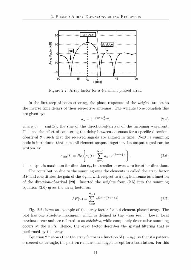
Figure 2.2: Array factor for a 4-element phased array.
In the first step of beam steering, the phase responses of the weights are set to
the inverse time delays of their respective antennas. The weights to accomplish this
are given by:
an = e−j2π·ndλu0 , (2.5)
where u0 = sin(θ0), the sine of the direction-of-arrival of the incoming wavefront.
This has the effect of countering the delay between antennas for a specific direction-
of-arrival θ0, such that the received signals are aligned in time. Next, a summing
node is introduced that sums all element outputs together. Its output signal can be
written as:
sout(t) = Re
s0(t) ·
N−1∑n=0
an · ej2π·ndλu
. (2.6)
The output is maximum for direction θ0, but smaller or even zero for other directions.
The contribution due to the summing over the elements is called the array factor
AF and constitutes the gain of the signal with respect to a single antenna as a function
of the direction-of-arrival [29]. Inserted the weights from (2.5) into the summing
equation (2.6) gives the array factor as:
AF (u) =
N−1∑n=0
ej2π·ndλ (u−u0). (2.7)
Fig. 2.2 shows an example of the array factor for a 4-element phased array. The
plot has one absolute maximum, which is defined as the main beam. Lower local
maxima occur and are referred to as sidelobes, while completely destructive summing
occurs at the nulls. Hence, the array factor describes the spatial filtering that is
performed by the array.
Equation 2.7 shows that the array factor is a function of (u−u0), so that if a pattern
is steered to an angle, the pattern remains unchanged except for a translation. For this
11

2. Phased-Array Downconverting Receivers
−1 −0.5 0 0.5 1−40
−20
0
20
40
u=sin(θ)
AF
[d
B]
d/λ=0.3
d/λ=0.5
d/λ=1.0
(a)
0.2
0.4
0.6
0.8
1.0
30
210
60
240
90
270
120
300
150
330
180 0
d/λ=0.5
(b)
Figure 2.3: Array factor for an 8-element phased array steered to u0 = 0.5.
reason the variables u and u0 are used, in sine space [30]. A closed form expression
for the array factor of a uniformly illuminated array (|an| = 1) steered to direction
u0 can be found [30]:
AFuni,u0(u) =
sin[N · π dλ (u− u0)
]sin[π dλ (u− u0)
]︸ ︷︷ ︸Amplitude
· ejπ dλ (N−1)·(u−u0)︸ ︷︷ ︸Phase
. (2.8)
Fig. 2.3 plots this antenna factor for several values of d/λ. As the antenna spacing
with respect to the wavelength increases, the width of the main beam decreases due
to the increased effective length L of the array:
L = N · d (2.9)
The half-power or -3 dB width of the beam can be calculated to be [31]:
u−3dB = 0.886λ
L. (2.10)
For achieving the narrowest beam width, it is therefore essential to increase the
antenna spacing as much as possible. However, there is a point where additional
main beams, the grating lobes, occur in directions other than θ0. These beams are
positioned at locations [32]:
u = u0 + i · λd, i = ..,−2,−1, 0, 1, 2, .. (2.11)
So that in order to avoid grating lobes, the maximum antenna spacing for a full scan
range is:d
λmin≤ 1
2(2.12)
12
2. Phased-Array Downconverting Receivers
−1 −0.5 0 0.5 1−40
−20
0
20
40
u=sin(θ)
AF
[d
B]
f0/f=0.75
f0/f=1.0
f0/f=1.25
(a)
−1 −0.5 0 0.5 1−40
−20
0
20
40
u=sin(θ)
AF
[d
B]
f0/f=0.75
f0/f=1.0
f0/f=1.25
(b)
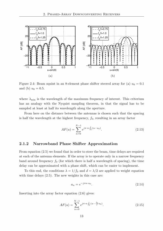
Figure 2.4: Beam squint in an 8-element phase shifter steered array for (a) u0 = 0.1
and (b) u0 = 0.5.
where λmin is the wavelength of the maximum frequency of interest. This criterium
has an analogy with the Nyquist sampling theorem, in that the signal has to be
sampled at least at half its wavelength along the aperture.
From here on the distance between the antennas is chosen such that the spacing
is half the wavelength at the highest frequency, f0, resulting in an array factor
AF (u) =
N−1∑n=0
ejπ·nff0
(u−u0). (2.13)
2.1.2 Narrowband Phase Shifter Approximation
From equation (2.5) we found that in order to steer the beam, time delays are required
at each of the antenna elements. If the array is to operate only in a narrow frequency
band around frequency f0 (for which there is half a wavelength of spacing), the time
delay can be approximated with a phase shift, which can be easier to implement.
To this end, the conditions λ = 1/f0 and d = λ/2 are applied to weight equation
with time delays (2.5). The new weights in this case are:
an = e−jπn·u0 . (2.14)
Inserting into the array factor equation (2.6) gives:
AF (u) =
N−1∑n=0
ejπ·nff0
(u− f0f u0). (2.15)
13

2. Phased-Array Downconverting Receivers
Defining the frequency deviation ∆f = f0 − f , this can be rewritten as:
AF (u) =
N−1∑n=0
ejπ·nff0
(u−(1+ ∆ff )u0) =
N−1∑n=0
ejπ·nff0
(u−u0) · e−jπ·n∆ff0u0︸ ︷︷ ︸
Excess phase
. (2.16)
Compared to the array factor with time delays (2.13), the location of the main beam
is now frequency dependent:
u′0(f) = (1 +∆f
f)u0, (2.17)
as a result of the excess phase in (2.16) [33]. Defining the shift in location as ∆u(f):
u′0(f) = u0 + ∆u ⇒ ∆u(f)
u0=
∆f
f. (2.18)
Or stated in words, the fractional shift in main beam position is equal to the fractional
shift in frequency [30]. This behavior is known as beam squint. It increases for larger
steering angles and for larger frequency differences, as is illustrated in Fig. 2.4. When
considered in a single direction, the gain of the array is now frequency dependent,
with 3 dB attenuation at the point where ∆u(f) = u−3dB (applying equation (2.10)).
Therefore, the bandwidth of a phased array steered with phase shifters is inherently
limited, regardless of the electrical bandwidth of the circuits:
BW−3dB = fu−3dB
u0≈ f0
2
u0N. (2.19)
The fractional bandwidth for a full scan range is thus inversely proportional to the
number of antennas.
2.1.3 Directivity
It can be shown that the element weights and array factor form the Fourier series pair
[30]:
an =1
2
∫ 1
−1
AF (u) · e−jπ·n·udu (2.20)
AF (u) =
N−1∑n=0
an · ejπ·n·u. (2.21)
For such a pair, the power in one domain (AF (u)) is equal to the power in the other
domain (an), so that Parseval’s theorem can be applied:
N−1∑n=0
|an|2 =
∫ 1
−1
|AF (u)|2du. (2.22)
14
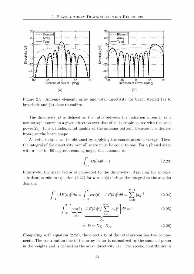
2. Phased-Array Downconverting Receivers
−90 −45 0 45 90−40
−30
−20
−10
0
10
20
30
Direction of arrival θ [deg]
Dire
ctivity [dB
]
Element
Array
Total
(a)
−90 −45 0 45 90−40
−30
−20
−10
0
10
20
30
Direction of arrival θ [deg]
Dire
ctivity [dB
]
Element
Array
Total
(b)
Figure 2.5: Antenna element, array and total directivity for beam steered (a) to
broadside and (b) close to endfire.
The directivity D is defined as the ratio between the radiation intensity of a
nonisotropic source in a given direction over that of an isotropic source with the same
power[29]. It is a fundamental quality of the antenna pattern, because it is derived
from just the beam shape.
A useful insight can be obtained by applying the conservation of energy. Then,
the integral of the directivity over all space must be equal to one. For a phased array
with a +90 to -90 degrees scanning angle, this amounts to:∫ π
−πD(θ)dθ = 1. (2.23)
Intuitively, the array factor is connected to the directivity. Applying the integral
substitution rule to equation (2.22) for u = sin(θ) brings the integral to the angular
domain: ∫ 1
−1
|AF (u)|2du =
∫ π
−πcos(θ) · |AF (θ)|2dθ =
N−1∑n=0
|an|2 (2.24)
∫ π
−π
[cos(θ)︸ ︷︷ ︸DE
· |AF (θ)|2/N−1∑n=0
|an|2︸ ︷︷ ︸DA
]dθ = 1 (2.25)
⇒ D = DE ·DA. (2.26)
Comparing with equation (2.23), the directivity of the total system has two compo-
nents. The contribution due to the array factor is normalized by the summed power
in the weights and is defined as the array directivity DA. The second contribution is
15
2. Phased-Array Downconverting Receivers
q
a0
a1
a2
a3
SIN
NIN
SIN
NIN
SIN
NIN
SIN
NIN
SOUT
NOUT
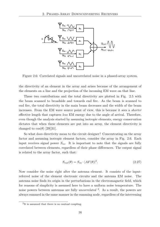
Figure 2.6: Correlated signals and uncorrelated noise in a phased-array system.
the directivity of an element in the array and arises because of the arrangement of
the elements on a line and the projection of the incoming EM wave on that line.
These two contributions and the total directivity are plotted in Fig. 2.5 with
the beam scanned to broadside and towards end fire. As the beam is scanned to
end fire, the total directivity in the main beam decreases and the width of the beam
increases. From the EM wave source point of view, this is because it sees a shorter
effective length that captures less EM energy due to the angle of arrival. Therefore,
even though the analysis started by assuming isotropic elements, energy conservation
dictates that when these elements are put into an array, the element directivity is
changed to cos(θ) [29][31].
So what does directivity mean to the circuit designer? Concentrating on the array
factor and assuming isotropic element factors, consider the array in Fig. 2.6. Each
input receives signal power Sin. It is important to note that the signals are fully
correlated between elements, regardless of their phase differences. The output signal
is related to the array factor, such that:
Sout(θ) = Sin · |AF (θ)|2. (2.27)
Now consider the noise right after the antenna element. It consists of the input-
referred noise of the element electronic circuits and the antenna EM noise. The
antenna noise finds its origin in the perturbations in the electromagnetic field, which
for reasons of simplicity is assumed here to have a uniform noise temperature. The
noise powers between antennas are fully uncorrelated 2. As a result, the powers are
always summed in the same manner in the summing node, regardless of the intervening
2It is assumed that there is no mutual coupling.
16
2. Phased-Array Downconverting Receivers
phase shifts and it can be stated that for all angles:
Nout = Nin ·N−1∑n=0
|an|2. (2.28)
If the ratio between signal power and noise power is taken:
SoutNout
(θ) =SinNin· |AF (θ)|2
/N−1∑n=0
|an|2 =SinNin·DA, (2.29)
it is found that directivity is the improvement in signal-to-noise ratio (SNR) compared
to a single isotropic antenna due to the directional properties of the aperture. In a
similar way, it can be proven that the same property holds for the element directivity
and for any other antenna aperture.
In publications, the element factor is usually not taken into account, because it
is fundamentally the same for all phased arrays, and only the array directivity is
reported. The maximum in array directivity can be found in the beam pointing
direction, where [31]:
max(DA) = |AF (θ0)|2/N−1∑n=0
|an|2 =
(N−1∑n=0
|an|
)2 /N−1∑n=0
|an|2 ≡ εT ·N, (2.30)
where εT is the taper efficiency (and equal to one for uniform tapering). In other
words, the maximum directivity occurs for a uniform taper and is equal to 10 · log(N)
dB.
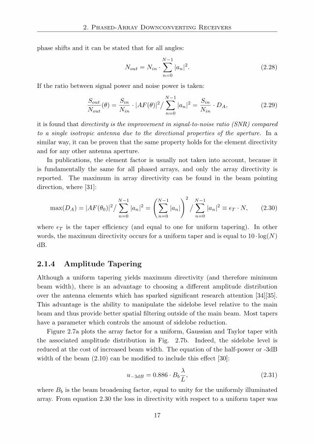
2.1.4 Amplitude Tapering
Although a uniform tapering yields maximum directivity (and therefore minimum
beam width), there is an advantage to choosing a different amplitude distribution
over the antenna elements which has sparked significant research attention [34][35].
This advantage is the ability to manipulate the sidelobe level relative to the main
beam and thus provide better spatial filtering outside of the main beam. Most tapers
have a parameter which controls the amount of sidelobe reduction.
Figure 2.7a plots the array factor for a uniform, Gaussian and Taylor taper with
the associated amplitude distribution in Fig. 2.7b. Indeed, the sidelobe level is
reduced at the cost of increased beam width. The equation of the half-power or -3dB
width of the beam (2.10) can be modified to include this effect [30]:
u−3dB = 0.886 ·Bbλ
L, (2.31)
where Bb is the beam broadening factor, equal to unity for the uniformly illuminated
array. From equation 2.30 the loss in directivity with respect to a uniform taper was
17
2. Phased-Array Downconverting Receivers
−1 −0.5 0 0.5 1−30
−20
−10
0
10
20
30
40
50
AF
[d
B]
u=sin(θ)
Uniform
Gaussian, α=1.2
Taylor, −30dB, n=5
(a)
0 2 4 6 8 100
0.5
1
1.5
2
2.5
Am
plit
ud
e |a
n|
Element position n
Uniform
Gaussian, α=1.2
Taylor, −30dB, n=5
(b)
Figure 2.7: 12-element (a) array factor and (b) amplitude distribution for three am-
plitude tapers.
expressed in the taper efficiency εT , which can be rewritten as:
1
εT= 1 +
1
N
∑(|an|
mean|an|− 1
)2
. (2.32)
This equation states that the taper efficiency is always smaller than one and worsens
when the amplitudes deviate more from the mean amplitude. For the specific Gaus-
sian and Taylor tapers shown in the picture, the taper efficiency is -0.2 and -0.7 dB
respectively, with a beam broadening factor of 1.12 and 1.26 respectively.
The choice for a specific taper type is determined by its particular properties.
For example, a Chebychev taper has equal sidelobe levels but has an impractical
amplitude distribution for large arrays (which are mitigated in the derived Taylor
taper), while the Gaussian taper provides the optimum balance between beam width
and overall sidelobe level3. Amplitude tapering is most effective for large arrays which
have pencil beams and where the sidelobes dominate the array factor.
2.1.5 Null Steering
In a receiver environment with few antenna elements, amplitude tapering is less ef-
fective, as the main beam will widen significantly. For example, in a 4 element array,
the two sidelobes are -10 dB below the main beam, resulting in a modest rejection.
However, in the case of a single dominant interferer, the rejection can be signifi-
cantly increased if a null would be adaptively steered on its direction. It is assumed
that the direction of the interferer is known a-priori or is determined by an additive
3 The uniform taper is just a special case of the Gaussian taper with α = 0.
18
2. Phased-Array Downconverting Receivers
−1 −0.5 0 0.5 1
−20
−10
0
10
20
u=sin(θ)
Arr
ay F
acto
r [d
B]
uint
u0
AFquies
AFint
(a)
−1 −0.5 0 0.5 1
−20
−10
0
10
20
u=sin(θ)
Arr
ay F
acto
r [d
B]
uint
u0
AFnull
= AFquies
−AFint
(b)
Figure 2.8: Subtraction of (a) interferer pattern AFint from quiescent pattern AFquies
results in (b) an array factor with a null on the interferer position.
steering algorithm. From the beamforming properties analyzed in this chapter so far,
it is clear that the position of the nulls is rather fixed with respect to the main beam.
Therefore, a different kind of pattern synthesis is required.
A graphical representation of the beam pattern synthesis to enable null steering is
illustrated in Fig. 2.8a [36]. The goal is to adapt the regular beam pattern AFquies,
steered towards the location of the signal-of-interest u0, such that it has a null on the
location of the interferer, uint.
In order to do so, we rely on the linear properties of the array factor, i.e. a
linear combination of array factors is equal to a single array factor with the same
linear combination of the weights. If two array factors can be created such that their
subtraction creates a null on the desired location, then the subtraction of the weights
for these array factors will result in new weights for a single array factor with the
same nulling.
The cancellation array factor, AFint, is introduced with main beam at the location
of the interferer, uint, and scaled to the height of the quiescent array factor at uint.
Therefore, subtraction of the quiescent and cancellation array factor will result in a
new array factor with a null at the interferer location, as shown in Fig. 2.8b. This
new array factor is:
AFnull(u) = AFquies(u)−AFint(u) = AFuni,u0(u)−AFuni,u0
(uint) ·1
NAFuni,uint
(u)
(2.33)
Inserting the array factor for uniform tapering (2.8):
AFnull(u) =
N−1∑n=0
ejπn(u−u0) −sin[N · π2 (uint − u0)
]N · sin
[π2 (uint − u0)
]ejπN−12 (uint−u0) ·
N−1∑n=0
ejπn(u−uint)
(2.34)
19

2. Phased-Array Downconverting Receivers
−1 −0.5 0 0.5 1−30
−20
−10
0
10
20
Arr
ay F
acto
r [d
B]
u=sin(θ)
(a)
0.2
0.4
0.6
0.8
1.0
1.2
30
210
60
240
90
270
120
300
150
330
180 0
(b)
Figure 2.9: Adaptive nulling (a) array factors and (b) element weights with main
beam at u = 0.5 and interferer direction swept from u = −1 to u = 0.1.
And some reordering gives the total array factor as:
AFnull(u) =
N−1∑n=0
(e−jπn·u0 −
sin[N · π2 (uint − u0)
]N · sin
[π2 (uint − u0)
] · ejπ(N−12 ·(uint−u0)−n·uint)
)︸ ︷︷ ︸
an
·ejπnu
(2.35)
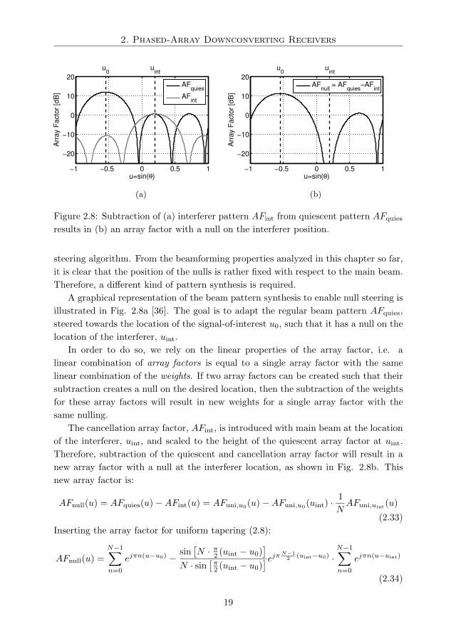
From Fig. 2.8a, it can be deduced that the main beam remains largely unaffected
as long as the interferer has a sufficiently different angle-of-arrival, as the main beam
is in the sidelobe of the cancellation pattern. In a worst case scenario the interferer
is at a quiescent pattern sidelobe, being scaled 10 dB below the main beam to ensure
nulling. At the main beam, the cancellation sidelobe is another 10 dB lower, resulting
after subtraction in at most a modest -1 dB gain loss. This is illustrated in Fig. 2.9a,
which plots the array factors of the adaptive nulling algorithm for different interferer
directions.
Similarly, from (2.35) it can be deduced that the resulting element weights for null
steering are a small perturbation of the original weights for beam steering (Fig. 2.9b).
The scaling of the cancellation pattern results in the second part of the subtraction
having an amplitude between zero and one-third, whereas the first part of the sub-
traction has unity amplitude. Therefore, the resulting amplitudes |an| are close to
unity themselves.
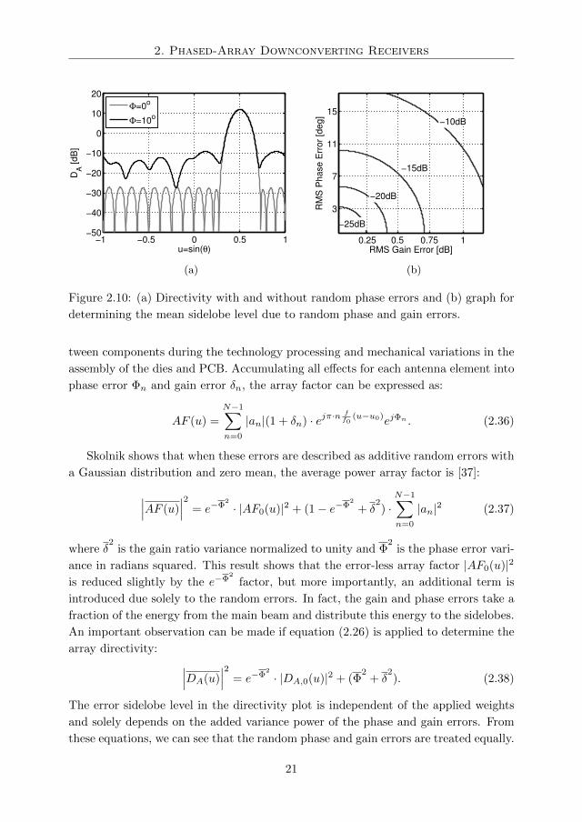
2.1.6 Random Errors
In practice, a phased-array implementation cannot provide the exact phase and gain
response that are desired for the beamforming pattern. There are mismatches be-
20
2. Phased-Array Downconverting Receivers
−1 −0.5 0 0.5 1−50
−40
−30
−20
−10
0
10
20
DA [
dB
]
u=sin(θ)
Φ=0o
Φ=10o
(a)
RMS Gain Error [dB]
RM
S P
hase E
rror
[deg]
−25dB
−20dB
−15dB
−10dB
0.25 0.5 0.75 1
3
7
11
15
(b)
Figure 2.10: (a) Directivity with and without random phase errors and (b) graph for
determining the mean sidelobe level due to random phase and gain errors.
tween components during the technology processing and mechanical variations in the
assembly of the dies and PCB. Accumulating all effects for each antenna element into
phase error Φn and gain error δn, the array factor can be expressed as:
AF (u) =
N−1∑n=0
|an|(1 + δn) · ejπ·nff0
(u−u0)ejΦn . (2.36)
Skolnik shows that when these errors are described as additive random errors with
a Gaussian distribution and zero mean, the average power array factor is [37]:
∣∣∣AF (u)∣∣∣2 = e−Φ
2
· |AF0(u)|2 + (1− e−Φ2
+ δ2) ·
N−1∑n=0
|an|2 (2.37)
where δ2
is the gain ratio variance normalized to unity and Φ2
is the phase error vari-
ance in radians squared. This result shows that the error-less array factor |AF0(u)|2
is reduced slightly by the e−Φ2
factor, but more importantly, an additional term is
introduced due solely to the random errors. In fact, the gain and phase errors take a
fraction of the energy from the main beam and distribute this energy to the sidelobes.
An important observation can be made if equation (2.26) is applied to determine the
array directivity: ∣∣∣DA(u)∣∣∣2 = e−Φ
2
· |DA,0(u)|2 + (Φ2
+ δ2). (2.38)
The error sidelobe level in the directivity plot is independent of the applied weights
and solely depends on the added variance power of the phase and gain errors. From
these equations, we can see that the random phase and gain errors are treated equally.
21

2. Phased-Array Downconverting Receivers
This stands to reason as it is the combined error distance in the phasor diagram that
is relevant for constructive and destructive summing.
As an example, Fig. 2.10a plots the array directivity with and without random
phase errors. Indeed, the errors increase the sidelobe level while the main beam is
almost unaffected. In order to estimate the average sidelobe level, Fig. 2.10b plots
(Φ2
+ δ2) on a dB scale. For the plotted 10 of phase error variance, this graph
indicates a -15 dB average sidelobe level, which is in correspondence with Fig. 2.10a.
In most cases it is not the average sidelobe level, but the peak sidelobe level relative
to the main beam which is of interest. In the directivty plot, the main beam increases
with 10·log(N), so that the relative sidelobe level increases with the number of antenna
elements. Moreover, Allen has shown that over-designing the average sidelobe level to
be 10 dB below the desired peak sidelobe level is sufficient to ensure good operation
in practical cases [38]. This gives the following expression for the sidelobe level SL
relative to the main beam.
SL < 10 · log(
Φ2
+ δ2)− 10 · log(N) + 10 [dB] (2.39)
For example, a 4-element array with 2 root-mean-square (RMS) phase error and 0.2
dB RMS gain error will have its error sidelobes more than 20 dB below the main
beam. In the case of few antenna elements and adaptive pattern nulling, the same
design equations can be used to determine the null depths that can be guaranteed.
2.1.7 Phase Quantization Errors
For half λ antenna spacing and practical tapers, the beam width can be approximated
as (2.10):
u−3dB ≈2
N. (2.40)
In u-space a complete sweep of the beam goes in steps of u−3dB from u = −1 to u = 1,
so that N beams can cover the entire sweep span, with a 3 dB ripple on reception
(Fig. 2.11a):
u0 = −1 +2i
N, i = 0, 1, 2, .., N − 1 (2.41)
From the phase shifter weights in narrowband arrays (2.14) we find that the smallest
phase steps are for the beam which is pointed one beam width away from broadside
(i = N ±1). If the phase steps are not small enough, they have to be rounded off and
groups of elements with the same phase shift occur, resulting in grating lobes (Fig.
2.11b). So, for a -3 dB scan range in an N-element array without grating lobes, the
minimum of uniformly quantized phase shifter steps is N.
If the required phase shifter steps are not available, quantization lobes will occur
in the array factor. Miller has considered the quantization lobe level for a continuous
22
2. Phased-Array Downconverting Receivers
−1 −0.5 0 0.5 1
−20
0
20
u=sin(θ)
AF
[d
B]
0 5 10 15
−180
−90
0
90
180
Element position
Pha
se S
hift [d
eg]
(a)
−1 −0.5 0 0.5 1
−20
0
20
u=sin(θ)
AF
[d
B]
0 5 10 15
−180
−90
0
90
180
Element position
Ph
ase
Shift[
deg]
(b)
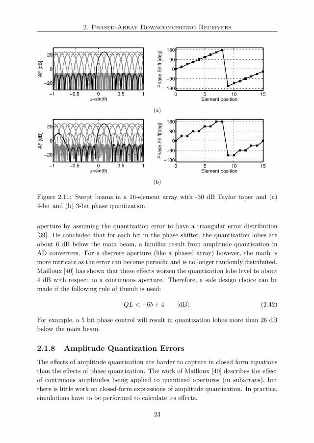
Figure 2.11: Swept beams in a 16-element array with -30 dB Taylor taper and (a)
4-bit and (b) 3-bit phase quantization.
aperture by assuming the quantization error to have a triangular error distribution
[39]. He concluded that for each bit in the phase shifter, the quantization lobes are
about 6 dB below the main beam, a familiar result from amplitude quantization in
AD converters. For a discrete aperture (like a phased array) however, the math is
more intricate as the error can become periodic and is no longer randomly distributed.
Mailloux [40] has shown that these effects worsen the quantization lobe level to about
4 dB with respect to a continuous aperture. Therefore, a safe design choice can be
made if the following rule of thumb is used:
QL < −6b+ 4 [dB]. (2.42)
For example, a 5 bit phase control will result in quantization lobes more than 26 dB
below the main beam.
2.1.8 Amplitude Quantization Errors
The effects of amplitude quantization are harder to capture in closed form equations
than the effects of phase quantization. The work of Mailloux [40] describes the effect
of continuous amplitudes being applied to quantized apertures (in subarrays), but
there is little work on closed-form expressions of amplitude quantization. In practice,
simulations have to be performed to calculate its effects.
23
2. Phased-Array Downconverting Receivers
?
?
?
?
?
?
?
?
fLO
fLO
fLO
fLO
X Y
j0
j1
j2
j3
(a)
f
j
j0
j1
j2
j3
(b)
Figure 2.12: (a) Beamforming system with downconversion and (b) phases of the
incoming signals as a function of frequency.
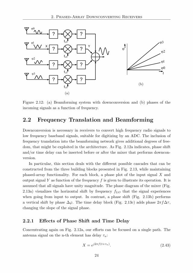
2.2 Frequency Translation and Beamforming
Downconversion is necessary in receivers to convert high frequency radio signals to
low frequency baseband signals, suitable for digitizing by an ADC. The inclusion of
frequency translation into the beamforming network gives additional degrees of free-
dom, that might be exploited in the architecture. As Fig. 2.12a indicates, phase shift
and/or time delay can be inserted before or after the mixer that performs downcon-
version.
In particular, this section deals with the different possible cascades that can be
constructed from the three building blocks presented in Fig. 2.13, while maintaining
phased-array functionality. For each block, a phase plot of the input signal X and
output signal Y as function of the frequency f is given to illustrate its operation. It is
assumed that all signals have unity magnitude. The phase diagram of the mixer (Fig.
2.13a) visualizes the horizontal shift by frequency fLO that the signal experiences
when going from input to output. In contrast, a phase shift (Fig. 2.13b) performs
a vertical shift by phase ∆ϕ. The time delay block (Fig. 2.13c) adds phase 2πf∆τ ,
changing the slope of the signal phase.
2.2.1 Effects of Phase Shift and Time Delay
Concentrating again on Fig. 2.12a, our efforts can be focused on a single path. The
antenna signal on the n-th element has delay τn:
X = ej2πf(t+τn). (2.43)
24
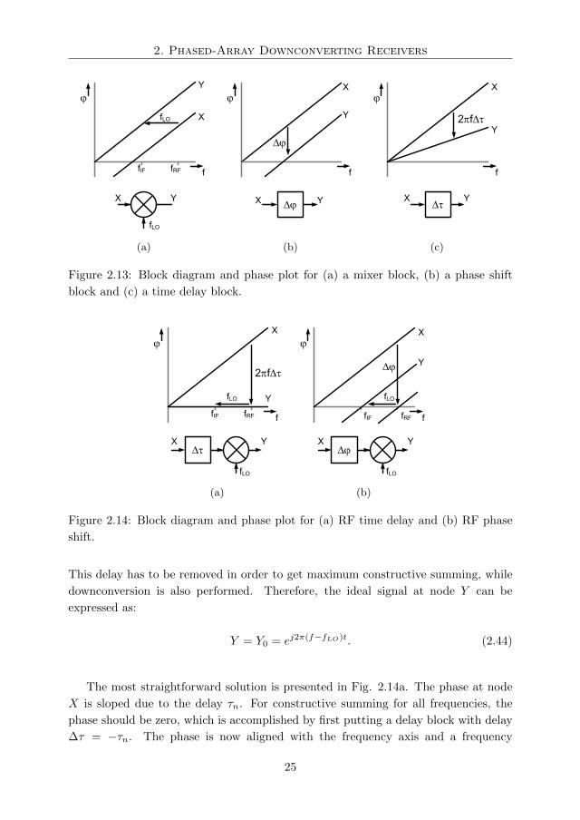
2. Phased-Array Downconverting Receivers
X Y
fLO
f
j
fRFfIF
fLO X
Y
(a)
X YDj
f
j
Dj
X
Y
(b)
X YDt
f
j
2pfDt
X
Y
(c)
Figure 2.13: Block diagram and phase plot for (a) a mixer block, (b) a phase shift
block and (c) a time delay block.
X YDt
fLO
f
j
fRFfIF
fLO
2pfDt
X
Y
(a)
X YDj
fLO
f
j
fRFfIF
fLO
Dj
X
Y
(b)
Figure 2.14: Block diagram and phase plot for (a) RF time delay and (b) RF phase
shift.
This delay has to be removed in order to get maximum constructive summing, while
downconversion is also performed. Therefore, the ideal signal at node Y can be
expressed as:
Y = Y0 = ej2π(f−fLO)t. (2.44)
The most straightforward solution is presented in Fig. 2.14a. The phase at node
X is sloped due to the delay τn. For constructive summing for all frequencies, the
phase should be zero, which is accomplished by first putting a delay block with delay
∆τ = −τn. The phase is now aligned with the frequency axis and a frequency
25

2. Phased-Array Downconverting Receivers
X YDj
fLO
f
j
fRFfIF
fLO
Dj
X
Y
(a)
X YDt
fLO
f
j
fRFfIF
fLO X
Y
2pfDt
(b)
X YDj Dt
fLO
f
j
fRFfIF
fLO
2pfDt
Dj
X
Y
(c)
Figure 2.15: Block diagram and phase plot for (a) IF phase shift, (b) IF time delay
and (c) IF time delay + phase shift.
translation can be performed without disrupting the phase:
Y = ej2πf(t+τn) · ej2πf∆τ · e−j2πfLOt
= ej2π(f−fLO)t · ej2πf(τn+∆τ) = Y0 ,∆τ = −τn.(2.45)
In section 2.1.2, the use of phase shifters to approximate delay in a narrow band
was explored, resulting in beam squint. When the delay is replaced with a phase shift
(Fig. 2.14b), the output is:
Y = ej2πf(t+τn) · ej2π∆ϕ · e−j2πfLOt
= ej2π(f−fLO)t · ej2π(fτn+∆ϕ)(2.46)
The phase ϕ can only be made zero for a single center frequency ∆ϕ = 2πf0τn and
excess phase remains:
Y = ej2π(f−fLO)t · ej2π(f−f0)τn = Y0 · ej2π(f−f0)τn (2.47)
By realizing that τn = n u0
2f0and f − f0 = −∆f , it is seen that the excess phase
is equal to the previous analysis for phase shifter based arrays in equation (2.16).
The increasing phase deviation around the center frequency gives rise to the beam
squint. Moving the phase from the RF to the IF port of the mixer (Fig. 2.15a) results
in the same output Y , as the order of frequency translation and phase shift can be
exchanged. It can be stated that a mixer is transparent for phase.
However, if the time delay is moved from RF to IF (Fig. 2.15b), the phase plot
reveals that beam squint will appear. Where does the squint come from? Well, a
delay at RF frequencies gives a phase line through the origin of the phase plot, but
26

2. Phased-Array Downconverting Receivers
Type RF IF ∆ϕ ∆τ α
TD @ RF TD −τn 0
PS @ RF PS 2πf0τn 1
TD @ IF TD − f0
f0−fLO τnfLO
f0−fLOPS @ IF PS 2πf0τn 1
PS+TD @ IF PS+TD 2πfLOτn −τn 0
Table 2.1: Beam squint summary.
the downconversion shifts it off the origin:
Y = ej2πf(t+τn) · e−j2πfLOt · ej2π(f−fLO)∆τ
= ej2π(f−fLO)t · ej2π(fτn+f∆τ−fLO∆τ)(2.48)
Like the phase shift solution, the phase line can only go through zero for one frequency
f = f0:
Y = Y0 · ej2π(f−f0)fLO
f0−fLOτn ,∆τ =
f0
f0 − fLOτn (2.49)
and beam squint occurs for other frequencies. Therefore, it can be stated that a mixer
is not transparent for delay. Compared to (2.16), the excess phase has an additional
factor of f0
f0−fLO , so a time delay at IF will have a larger beam squint than a phase
shifter based array.
In order to eliminate the beam squint for IF time delays, an additional phase shift
is needed (Fig. 2.15c) to correct for the shift of the phase plot due to downconversion.
The horizontal shift in the plot by the downconversion is canceled by the vertical shift
of phase shifter, realigning the phase line with the origin. In mathematical form:
Y = ej2πf(t+τn) · e−j2πfLOt · e−j∆ϕ · ej2π(f−fLO)∆τ
= Y0 ,∆τ = −τn, ∆ϕ = 2π(f − fLO)τn.(2.50)
To summarize the beam squinting results for the different architectures, equation
(2.18) is modified with an additional α factor.
∆u(f)
u0= α
∆f
f(2.51)
Or in other words, the α parameter links the relative frequency deviation to the
relative beam shift. The results thus obtained are summarized in Table 2.1.
2.2.2 Transformations
In the analysis so far, only the RF and IF possibilities for phase shift and time delay
were considered. If the LO port of the mixer is also taken into account as an option to
27
2. Phased-Array Downconverting Receivers
-Dj
I1
Dj
(a)
-Dt
I2
Dt
(b)
Figure 2.16: Identities (a) I1 and (b) I2.
RF IF
LO
A3
DjRF IF
LO
Dj
RF
LO
Dj
IF
A1 A2
Figure 2.17: Transformation A1, A2 and A3.
insert a phase shift or time delay, the number of combinations increases many times.
A more practical approach is to find configurations that are equivalent, so that an
unfamiliar form can be transformed into a familiar one.
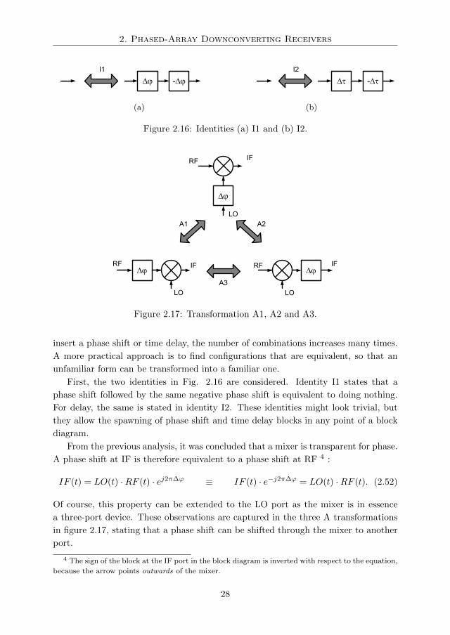
First, the two identities in Fig. 2.16 are considered. Identity I1 states that a
phase shift followed by the same negative phase shift is equivalent to doing nothing.
For delay, the same is stated in identity I2. These identities might look trivial, but
they allow the spawning of phase shift and time delay blocks in any point of a block
diagram.
From the previous analysis, it was concluded that a mixer is transparent for phase.
A phase shift at IF is therefore equivalent to a phase shift at RF 4 :
IF (t) = LO(t) ·RF (t) · ej2π∆ϕ ≡ IF (t) · e−j2π∆ϕ = LO(t) ·RF (t). (2.52)
Of course, this property can be extended to the LO port as the mixer is in essence
a three-port device. These observations are captured in the three A transformations
in figure 2.17, stating that a phase shift can be shifted through the mixer to another
port.
4 The sign of the block at the IF port in the block diagram is inverted with respect to the equation,
because the arrow points outwards of the mixer.
28
2. Phased-Array Downconverting Receivers
RF IFDt
LO
RF IF
Dt
LO
B1
Dt
(a)
RF IF
LO
RF IF
-Dt
LO
B2
Dt
Dt
(b)
RF IF
LO
RF IF
LO
B3
Dt
Dt
-Dt
(c)
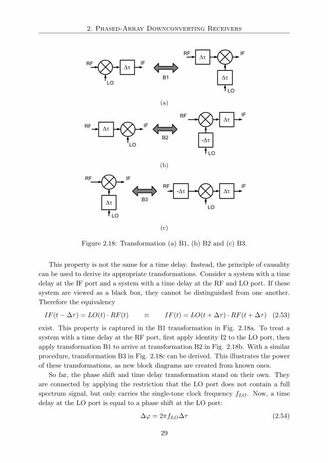
Figure 2.18: Transformation (a) B1, (b) B2 and (c) B3.
This property is not the same for a time delay. Instead, the principle of causality
can be used to derive its appropriate transformations. Consider a system with a time
delay at the IF port and a system with a time delay at the RF and LO port. If these
system are viewed as a black box, they cannot be distinguished from one another.
Therefore the equivalency
IF (t−∆τ) = LO(t) ·RF (t) ≡ IF (t) = LO(t+ ∆τ) ·RF (t+ ∆τ) (2.53)
exist. This property is captured in the B1 transformation in Fig. 2.18a. To treat a
system with a time delay at the RF port, first apply identity I2 to the LO port, then
apply transformation B1 to arrive at transformation B2 in Fig. 2.18b. With a similar
procedure, transformation B3 in Fig. 2.18c can be derived. This illustrates the power
of these transformations, as new block diagrams are created from known ones.
So far, the phase shift and time delay transformation stand on their own. They
are connected by applying the restriction that the LO port does not contain a full
spectrum signal, but only carries the single-tone clock frequency fLO. Now, a time
delay at the LO port is equal to a phase shift at the LO port:
∆ϕ = 2πfLO∆τ (2.54)
29
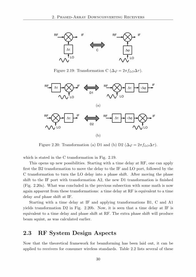
2. Phased-Array Downconverting Receivers
C
RF
LO
Dj
IFRF IF
LO
Dt
Figure 2.19: Transformation C (∆ϕ = 2πfLO∆τ).
RF IF
LO
RF IF
LO
D1
Dt Dt -Dj
(a)
RF IFDt
LOD2
RF
LO
-DjDtIF
(b)
Figure 2.20: Transformation (a) D1 and (b) D2 (∆ϕ = 2πfLO∆τ).
which is stated in the C transformation in Fig. 2.19.
This opens up new possibilities. Starting with a time delay at RF, one can apply
first the B2 transformation to move the delay to the IF and LO port, followed by the
C transformation to turn the LO delay into a phase shift. After moving the phase
shift to the IF port with transformation A2, the new D1 transformation is finished
(Fig. 2.20a). What was concluded in the previous subsection with some math is now
again apparent from these transformations: a time delay at RF is equivalent to a time
delay and phase shift at IF.
Starting with a time delay at IF and applying transformations B1, C and A1
yields transformation D2 in Fig. 2.20b. Now, it is seen that a time delay at IF is
equivalent to a time delay and phase shift at RF. The extra phase shift will produce
beam squint, as was calculated earlier.
2.3 RF System Design Aspects
Now that the theoretical framework for beamforming has been laid out, it can be
applied to receivers for consumer wireless standards. Table 2.2 lists several of these
30
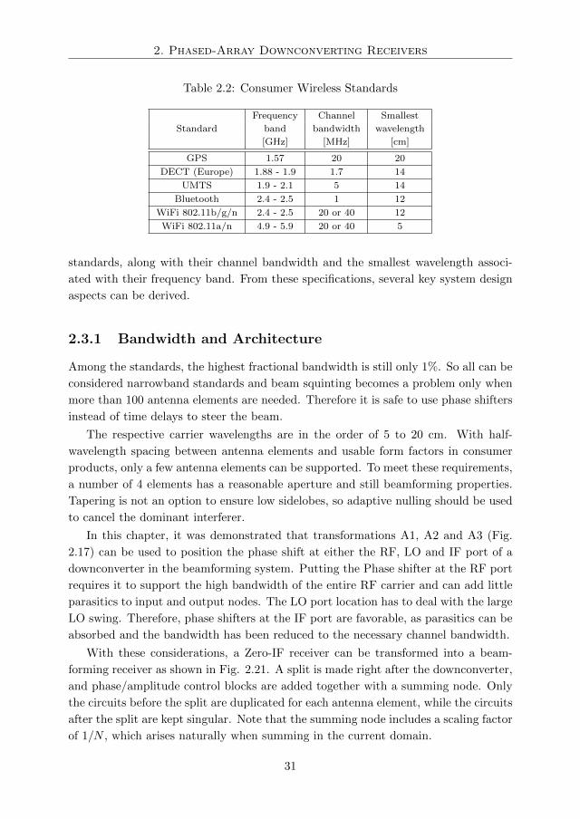
2. Phased-Array Downconverting Receivers
Table 2.2: Consumer Wireless Standards
Frequency Channel Smallest
Standard band bandwidth wavelength
[GHz] [MHz] [cm]
GPS 1.57 20 20
DECT (Europe) 1.88 - 1.9 1.7 14
UMTS 1.9 - 2.1 5 14
Bluetooth 2.4 - 2.5 1 12
WiFi 802.11b/g/n 2.4 - 2.5 20 or 40 12
WiFi 802.11a/n 4.9 - 5.9 20 or 40 5
standards, along with their channel bandwidth and the smallest wavelength associ-
ated with their frequency band. From these specifications, several key system design
aspects can be derived.
2.3.1 Bandwidth and Architecture
Among the standards, the highest fractional bandwidth is still only 1%. So all can be
considered narrowband standards and beam squinting becomes a problem only when
more than 100 antenna elements are needed. Therefore it is safe to use phase shifters
instead of time delays to steer the beam.
The respective carrier wavelengths are in the order of 5 to 20 cm. With half-
wavelength spacing between antenna elements and usable form factors in consumer
products, only a few antenna elements can be supported. To meet these requirements,
a number of 4 elements has a reasonable aperture and still beamforming properties.
Tapering is not an option to ensure low sidelobes, so adaptive nulling should be used
to cancel the dominant interferer.
In this chapter, it was demonstrated that transformations A1, A2 and A3 (Fig.
2.17) can be used to position the phase shift at either the RF, LO and IF port of a
downconverter in the beamforming system. Putting the Phase shifter at the RF port
requires it to support the high bandwidth of the entire RF carrier and can add little
parasitics to input and output nodes. The LO port location has to deal with the large
LO swing. Therefore, phase shifters at the IF port are favorable, as parasitics can be
absorbed and the bandwidth has been reduced to the necessary channel bandwidth.
With these considerations, a Zero-IF receiver can be transformed into a beam-
forming receiver as shown in Fig. 2.21. A split is made right after the downconverter,
and phase/amplitude control blocks are added together with a summing node. Only
the circuits before the split are duplicated for each antenna element, while the circuits
after the split are kept singular. Note that the summing node includes a scaling factor
of 1/N , which arises naturally when summing in the current domain.
31
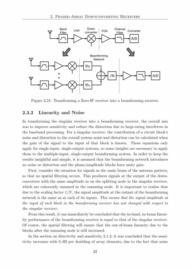
2. Phased-Array Downconverting Receivers
jn
N A/D
A/D
Channel
FilterVGA Converter
Down
converterLNA
Band
Filter
Beamforming
Network
j0
Figure 2.21: Transforming a Zero-IF receiver into a beamforming receiver.
2.3.2 Linearity and Noise
In transforming the singular receiver into a beamforming receiver, the overall aim
was to improve sensitivity and reduce the distortion due to large-swing interferers in
the baseband processing. For a singular receiver, the contribution of a circuit block’s
noise and distortion to the overall system noise and distortion can be calculated when
the gain of the signal to the input of that block is known. These equations only
apply for single-input, single-output systems, so some insights are necessary to apply
them to the multiple-input, single-output beamforming system. In order to keep the
results insightful and simple, it is assumed that the beamforming network introduces
no noise or distortion and the phase/amplitude blocks have unity gain.
First, consider the situation for signals in the main beam of the antenna pattern,
so that no spatial filtering occurs. This produces signals at the output of the down-
converters with the same amplitude as on the splitting node in the singular receiver,
which are coherently summed in the summing node. It is important to realize that
due to the scaling factor 1/N , the signal amplitude at the output of the beamforming
network is the same as at each of its inputs. This means that the signal amplitude at
the input of each block in the beamforming receiver has not changed with respect to
the singular receiver.
From this result, it can immediately be concluded that the in-band, in-beam linear-
ity performance of the beamforming receiver is equal to that of the singular receiver.
Of course, the spatial filtering will ensure that the out-of-beam linearity due to the
blocks after the summing node is still increased.
In the section on directivity and sensitivity 2.1.3, it was concluded that the sensi-
tivity increases with 3 dB per doubling of array elements, due to the fact that noise
32
2. Phased-Array Downconverting Receivers
adds non-coherently and signals add coherently in the summing node. To keep up
with the decreasing sensitivity of the circuits blocks before the beamforming network,
it can be found that the noise of the circuit blocks after the summing node has to also
decrease proportionally. From impedance scaling theory, it is known that noise and
supply power scale linearly as long as the impedance level is scaled accordingly, so
that a 3 dB increase of sensitivity corresponds to a doubling in supply power for the
circuits after the summing node. But, the doubling of the number of array elements
also corresponds to a doubling in supply power of the circuits before the summing
node, which can be explained as an alternate way of impedance scaling. So, an impor-
tant conclusion is reached: The sensitivity improvement from beamforming requires a
proportional increase in supply power, as with impedance scaling.
Impedance scaling a complete singular receiver usually does not work, as the
antenna impedance is fixed. For a beamforming receiver, it is as if the antennas are
in parallel and result in a virtual antenna with lower impedance.
2.4 Conclusions
The fundamental properties of linear phased arrays were summarized in the first part
of this chapter. The basic beam pattern was introduced and the effects on it by beam-
steering, amplitude tapering and the phase shifter approximation was summarized,
along with the degradation due to errors in the array.
Next, a framework for including downconversion in the beamforming architecture
has been presented, along with transformation methods to move time delay and/or
phase shift between the RF, LO and IF domain. It was found that the reallocation
of the beamforming to the LO or RF domain can give rise to beam squinting, as is
the case with the phase shifter approximation in general array theory. Furthermore,
the linearity and sensitivity properties of beamforming circuit implementations were
covered, concluding that beamforming can be viewed as a form of impedance scaling.
33
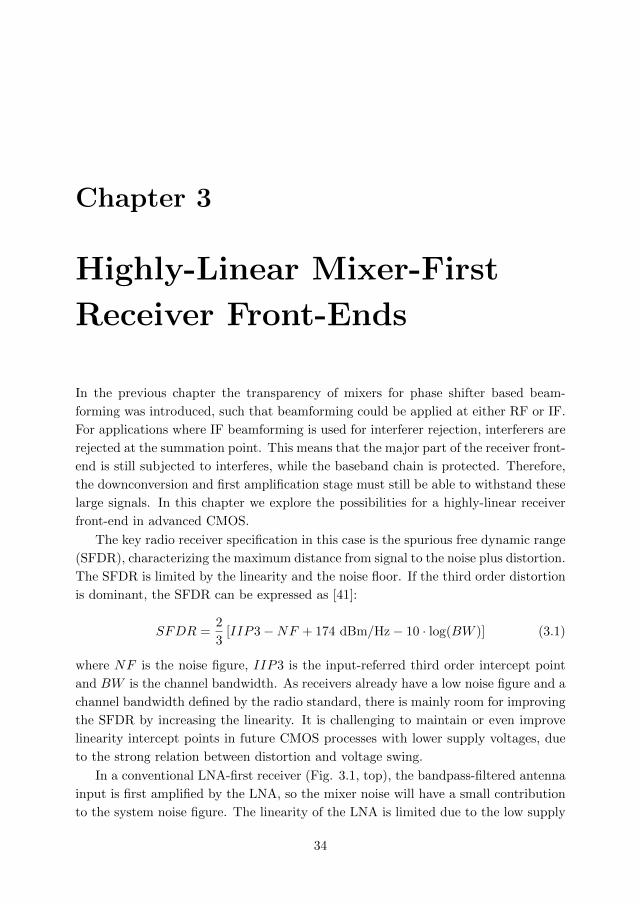
Chapter 3
Highly-Linear Mixer-First
Receiver Front-Ends
In the previous chapter the transparency of mixers for phase shifter based beam-
forming was introduced, such that beamforming could be applied at either RF or IF.
For applications where IF beamforming is used for interferer rejection, interferers are
rejected at the summation point. This means that the major part of the receiver front-
end is still subjected to interferes, while the baseband chain is protected. Therefore,
the downconversion and first amplification stage must still be able to withstand these
large signals. In this chapter we explore the possibilities for a highly-linear receiver
front-end in advanced CMOS.
The key radio receiver specification in this case is the spurious free dynamic range
(SFDR), characterizing the maximum distance from signal to the noise plus distortion.
The SFDR is limited by the linearity and the noise floor. If the third order distortion
is dominant, the SFDR can be expressed as [41]:
SFDR =2
3[IIP3−NF + 174 dBm/Hz− 10 · log(BW )] (3.1)
where NF is the noise figure, IIP3 is the input-referred third order intercept point
and BW is the channel bandwidth. As receivers already have a low noise figure and a
channel bandwidth defined by the radio standard, there is mainly room for improving
the SFDR by increasing the linearity. It is challenging to maintain or even improve
linearity intercept points in future CMOS processes with lower supply voltages, due
to the strong relation between distortion and voltage swing.
In a conventional LNA-first receiver (Fig. 3.1, top), the bandpass-filtered antenna
input is first amplified by the LNA, so the mixer noise will have a small contribution
to the system noise figure. The linearity of the LNA is limited due to the low supply
34
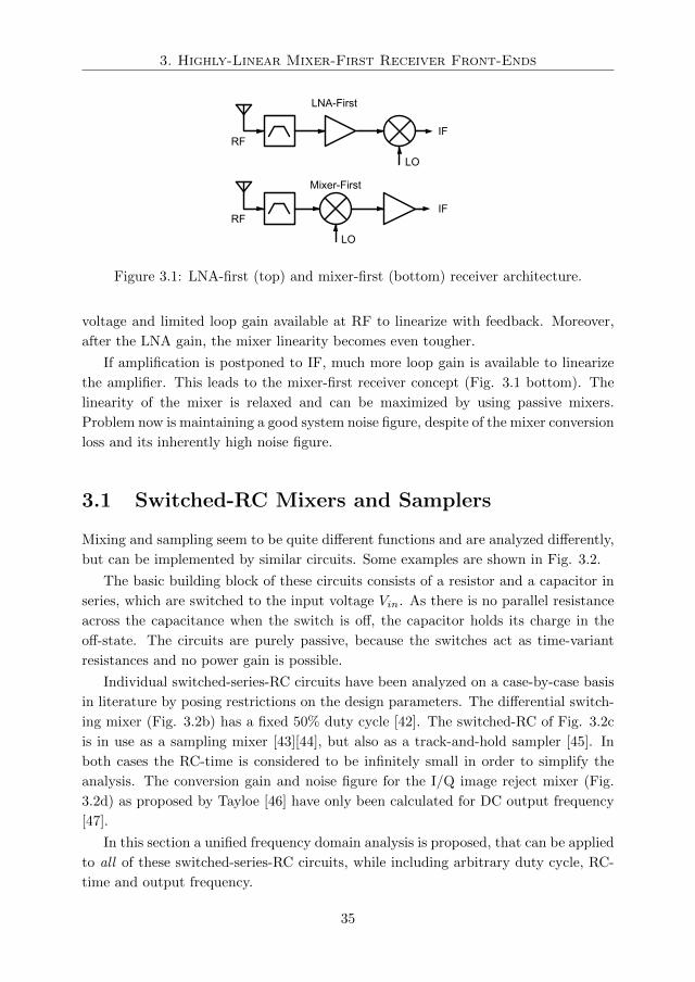
3. Highly-Linear Mixer-First Receiver Front-Ends
IF
LO
RF
IF
LO
RF
LNA-First
Mixer-First
Figure 3.1: LNA-first (top) and mixer-first (bottom) receiver architecture.
voltage and limited loop gain available at RF to linearize with feedback. Moreover,
after the LNA gain, the mixer linearity becomes even tougher.
If amplification is postponed to IF, much more loop gain is available to linearize
the amplifier. This leads to the mixer-first receiver concept (Fig. 3.1 bottom). The
linearity of the mixer is relaxed and can be maximized by using passive mixers.
Problem now is maintaining a good system noise figure, despite of the mixer conversion
loss and its inherently high noise figure.
3.1 Switched-RC Mixers and Samplers
Mixing and sampling seem to be quite different functions and are analyzed differently,
but can be implemented by similar circuits. Some examples are shown in Fig. 3.2.
The basic building block of these circuits consists of a resistor and a capacitor in
series, which are switched to the input voltage Vin. As there is no parallel resistance
across the capacitance when the switch is off, the capacitor holds its charge in the
off-state. The circuits are purely passive, because the switches act as time-variant
resistances and no power gain is possible.
Individual switched-series-RC circuits have been analyzed on a case-by-case basis
in literature by posing restrictions on the design parameters. The differential switch-
ing mixer (Fig. 3.2b) has a fixed 50% duty cycle [42]. The switched-RC of Fig. 3.2c
is in use as a sampling mixer [43][44], but also as a track-and-hold sampler [45]. In
both cases the RC-time is considered to be infinitely small in order to simplify the
analysis. The conversion gain and noise figure for the I/Q image reject mixer (Fig.
3.2d) as proposed by Tayloe [46] have only been calculated for DC output frequency
[47].
In this section a unified frequency domain analysis is proposed, that can be applied
to all of these switched-series-RC circuits, while including arbitrary duty cycle, RC-
time and output frequency.
35
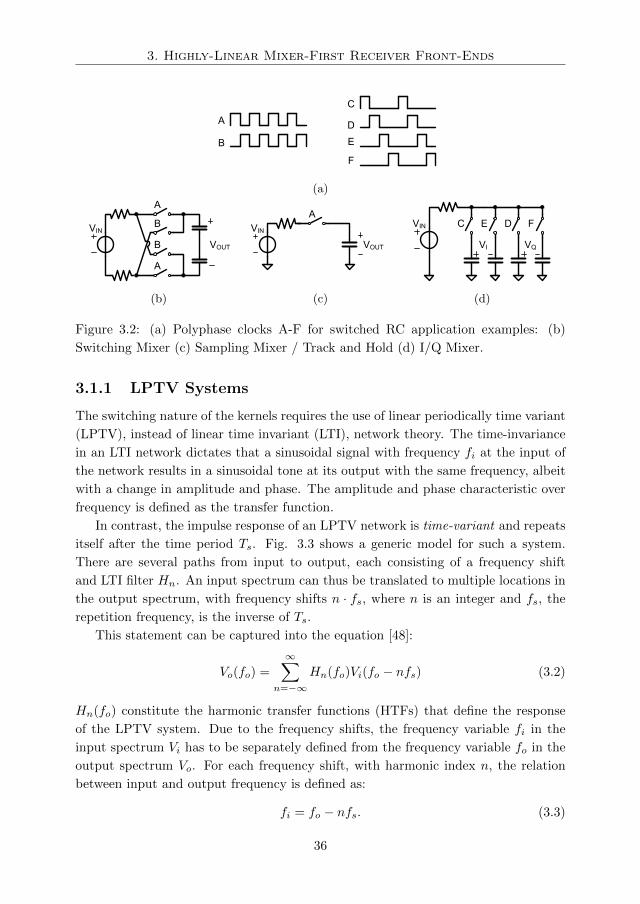
3. Highly-Linear Mixer-First Receiver Front-Ends
C
D
E
F
A
B
(a)
VIN
A
B
B
A
VOUT
(b)
VIN
A
VOUT
(c)
VIN
VI
EC
VQ
FD
(d)
Figure 3.2: (a) Polyphase clocks A-F for switched RC application examples: (b)
Switching Mixer (c) Sampling Mixer / Track and Hold (d) I/Q Mixer.
3.1.1 LPTV Systems
The switching nature of the kernels requires the use of linear periodically time variant
(LPTV), instead of linear time invariant (LTI), network theory. The time-invariance
in an LTI network dictates that a sinusoidal signal with frequency fi at the input of
the network results in a sinusoidal tone at its output with the same frequency, albeit
with a change in amplitude and phase. The amplitude and phase characteristic over
frequency is defined as the transfer function.
In contrast, the impulse response of an LPTV network is time-variant and repeats
itself after the time period Ts. Fig. 3.3 shows a generic model for such a system.
There are several paths from input to output, each consisting of a frequency shift
and LTI filter Hn. An input spectrum can thus be translated to multiple locations in
the output spectrum, with frequency shifts n · fs, where n is an integer and fs, the
repetition frequency, is the inverse of Ts.
This statement can be captured into the equation [48]:
Vo(fo) =
∞∑n=−∞
Hn(fo)Vi(fo − nfs) (3.2)
Hn(fo) constitute the harmonic transfer functions (HTFs) that define the response
of the LPTV system. Due to the frequency shifts, the frequency variable fi in the
input spectrum Vi has to be separately defined from the frequency variable fo in the
output spectrum Vo. For each frequency shift, with harmonic index n, the relation
between input and output frequency is defined as:
fi = fo − nfs. (3.3)
36
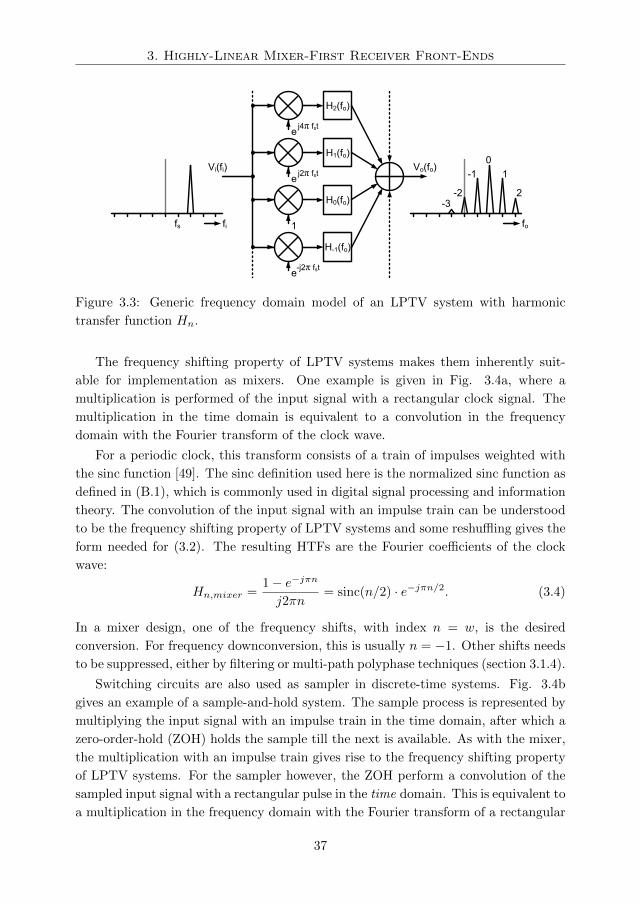
3. Highly-Linear Mixer-First Receiver Front-Ends
j4π fste
H2(fo)
j2π fste
H1(fo)
1
H0(fo)
-j2π fste
H-1(fo)
Vi(fi) Vo(fo)
fofifs
0
1-1
-2 2-3
Figure 3.3: Generic frequency domain model of an LPTV system with harmonic
transfer function Hn.
The frequency shifting property of LPTV systems makes them inherently suit-
able for implementation as mixers. One example is given in Fig. 3.4a, where a
multiplication is performed of the input signal with a rectangular clock signal. The
multiplication in the time domain is equivalent to a convolution in the frequency
domain with the Fourier transform of the clock wave.
For a periodic clock, this transform consists of a train of impulses weighted with
the sinc function [49]. The sinc definition used here is the normalized sinc function as
defined in (B.1), which is commonly used in digital signal processing and information
theory. The convolution of the input signal with an impulse train can be understood
to be the frequency shifting property of LPTV systems and some reshuffling gives the
form needed for (3.2). The resulting HTFs are the Fourier coefficients of the clock
wave:
Hn,mixer =1− e−jπn
j2πn= sinc(n/2) · e−jπn/2. (3.4)
In a mixer design, one of the frequency shifts, with index n = w, is the desired
conversion. For frequency downconversion, this is usually n = −1. Other shifts needs
to be suppressed, either by filtering or multi-path polyphase techniques (section 3.1.4).
Switching circuits are also used as sampler in discrete-time systems. Fig. 3.4b
gives an example of a sample-and-hold system. The sample process is represented by
multiplying the input signal with an impulse train in the time domain, after which a
zero-order-hold (ZOH) holds the sample till the next is available. As with the mixer,
the multiplication with an impulse train gives rise to the frequency shifting property
of LPTV systems. For the sampler however, the ZOH perform a convolution of the
sampled input signal with a rectangular pulse in the time domain. This is equivalent to
a multiplication in the frequency domain with the Fourier transform of a rectangular
37
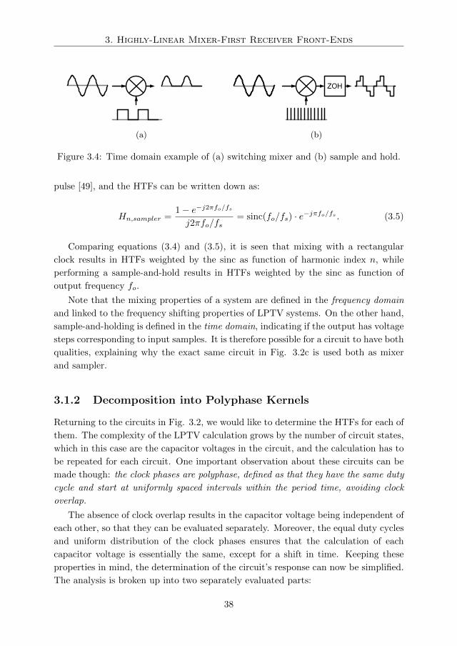
3. Highly-Linear Mixer-First Receiver Front-Ends
(a)
ZOH
(b)
Figure 3.4: Time domain example of (a) switching mixer and (b) sample and hold.
pulse [49], and the HTFs can be written down as:
Hn,sampler =1− e−j2πfo/fsj2πfo/fs
= sinc(fo/fs) · e−jπfo/fs . (3.5)
Comparing equations (3.4) and (3.5), it is seen that mixing with a rectangular
clock results in HTFs weighted by the sinc as function of harmonic index n, while
performing a sample-and-hold results in HTFs weighted by the sinc as function of
output frequency fo.
Note that the mixing properties of a system are defined in the frequency domain
and linked to the frequency shifting properties of LPTV systems. On the other hand,
sample-and-holding is defined in the time domain, indicating if the output has voltage
steps corresponding to input samples. It is therefore possible for a circuit to have both
qualities, explaining why the exact same circuit in Fig. 3.2c is used both as mixer
and sampler.
3.1.2 Decomposition into Polyphase Kernels
Returning to the circuits in Fig. 3.2, we would like to determine the HTFs for each of
them. The complexity of the LPTV calculation grows by the number of circuit states,
which in this case are the capacitor voltages in the circuit, and the calculation has to
be repeated for each circuit. One important observation about these circuits can be
made though: the clock phases are polyphase, defined as that they have the same duty
cycle and start at uniformly spaced intervals within the period time, avoiding clock
overlap.
The absence of clock overlap results in the capacitor voltage being independent of
each other, so that they can be evaluated separately. Moreover, the equal duty cycles
and uniform distribution of the clock phases ensures that the calculation of each
capacitor voltage is essentially the same, except for a shift in time. Keeping these
properties in mind, the determination of the circuit’s response can now be simplified.
The analysis is broken up into two separately evaluated parts:
38
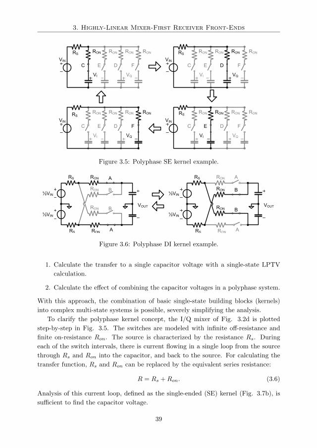
3. Highly-Linear Mixer-First Receiver Front-Ends
VIN
RS
VI
EC
VQ
FD
RONRONRONRON
VIN
RS
VI
EC
VQ
FD
RONRONRONRON
VIN
RS
VI
EC
VQ
FD
RONRONRONRON
VIN
RS
VI
EC
VQ
FD
RONRONRONRON
Figure 3.5: Polyphase SE kernel example.
½VIN
RS RON A
½VIN
RS RON A
RON B
RON BVOUT
½VIN
RS RON A
½VIN
RS RON A
RON B
RON BVOUT
Figure 3.6: Polyphase DI kernel example.
1. Calculate the transfer to a single capacitor voltage with a single-state LPTV
calculation.
2. Calculate the effect of combining the capacitor voltages in a polyphase system.
With this approach, the combination of basic single-state building blocks (kernels)
into complex multi-state systems is possible, severely simplifying the analysis.
To clarify the polyphase kernel concept, the I/Q mixer of Fig. 3.2d is plotted
step-by-step in Fig. 3.5. The switches are modeled with infinite off-resistance and
finite on-resistance Ron. The source is characterized by the resistance Rs. During
each of the switch intervals, there is current flowing in a single loop from the source
through Rs and Ron into the capacitor, and back to the source. For calculating the
transfer function, Rs and Ron can be replaced by the equivalent series resistance:
R = Rs +Ron. (3.6)
Analysis of this current loop, defined as the single-ended (SE) kernel (Fig. 3.7b), is
sufficient to find the capacitor voltage.
39
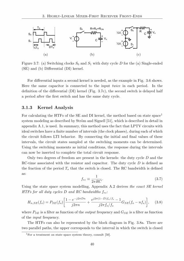
3. Highly-Linear Mixer-First Receiver Front-Ends
S0
S1
TS
DTS½TS
(a)
Vi
R=RS+RONS0
CVo
(b)
½ViR
S0C
Vo
½Vi S1
(c)
Figure 3.7: (a) Switching clocks S0 and S1 with duty cycle D for the (a) Single-ended
(SE) and (b) Differential (DI) kernel.
For differential inputs a second kernel is needed, as the example in Fig. 3.6 shows.
Here the same capacitor is connected to the input twice in each period. In the
definition of the differential (DI) kernel (Fig. 3.7c), the second switch is delayed half
a period after the first switch and has the same duty cycle.
3.1.3 Kernel Analysis
For calculating the HTFs of the SE and DI kernel, the method based on state space1
system modeling as described by Strom and Signell [51], which is described in detail in
appendix A.1, is used. In summary, this method uses the fact that LPTV circuits with
ideal switches have a finite number of intervals (the clock phases), during each of which
the circuit follows LTI behavior. By connecting the initial and final values of these
intervals, the circuit states sampled at the switching moments can be determined.
Using the switching moments as initial conditions, the response during the intervals
can now be inserted to complete the total circuit response.
Only two degrees of freedom are present in the kernels: the duty cycle D and the
RC-time associated with the resistor and capacitor. The duty cycle D is defined as
the fraction of the period Ts that the switch is closed. The RC bandwidth is defined
as:
frc ≡1
2πRC. (3.7)
Using the state space system modelling, Appendix A.2 derives the exact SE kernel
HTFs for all duty cycles D and RC bandwidths frc:
Hn,SE(fo) = PSE(fo)
[1− e−j2πDn
j2πn+ej2π(1−D)fo/fs − 1
j2πfo/fsGSE(fo − nfs)
], (3.8)
where PSE is a filter as function of the output frequency and GSE is a filter as function
of the input frequency.
The HTFs can also be represented by the block diagram in Fig. 3.8a. There are
two parallel paths, the upper corresponds to the interval in which the switch is closed
1For a treatment on state space system theory, consult [50].
40
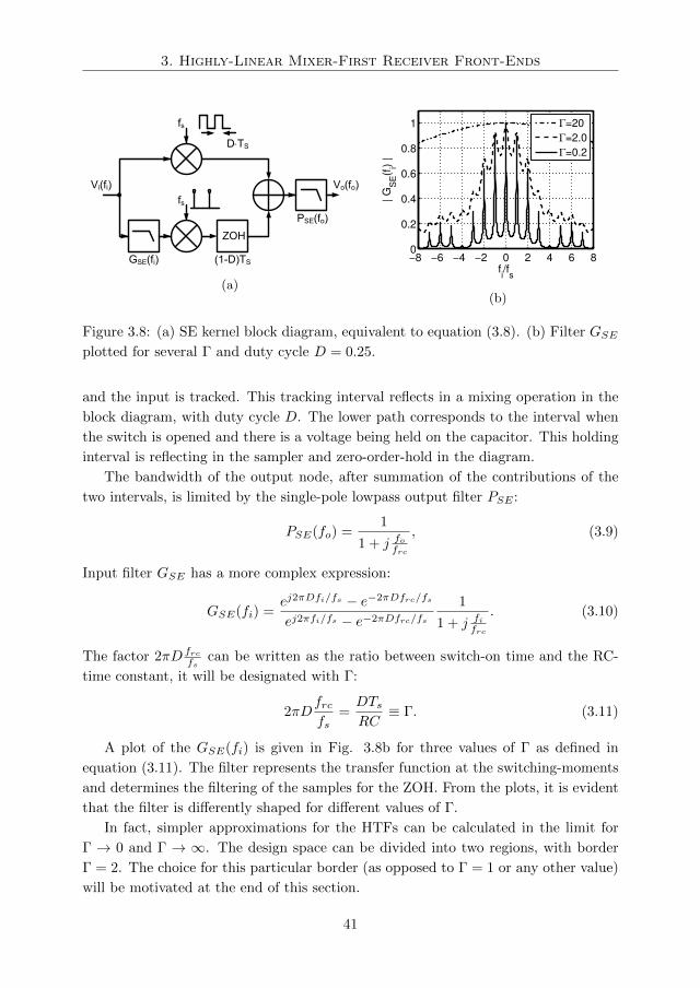
3. Highly-Linear Mixer-First Receiver Front-Ends
ZOH
Vi(fi) Vo(fo)
GSE(fi) (1-D)TS
fs
fs
PSE(fo)
D×TS
(a)
−8 −6 −4 −2 0 2 4 6 80
0.2
0.4
0.6
0.8
1
fi/f
s
| G
SE(f
i) |
Γ=20
Γ=2.0
Γ=0.2
(b)
Figure 3.8: (a) SE kernel block diagram, equivalent to equation (3.8). (b) Filter GSEplotted for several Γ and duty cycle D = 0.25.
and the input is tracked. This tracking interval reflects in a mixing operation in the
block diagram, with duty cycle D. The lower path corresponds to the interval when
the switch is opened and there is a voltage being held on the capacitor. This holding
interval is reflecting in the sampler and zero-order-hold in the diagram.
The bandwidth of the output node, after summation of the contributions of the
two intervals, is limited by the single-pole lowpass output filter PSE :
PSE(fo) =1
1 + j fofrc
, (3.9)
Input filter GSE has a more complex expression:
GSE(fi) =ej2πDfi/fs − e−2πDfrc/fs
ej2πfi/fs − e−2πDfrc/fs
1
1 + j fifrc
. (3.10)
The factor 2πD frcfs
can be written as the ratio between switch-on time and the RC-
time constant, it will be designated with Γ:
2πDfrcfs
=DTsRC
≡ Γ. (3.11)
A plot of the GSE(fi) is given in Fig. 3.8b for three values of Γ as defined in
equation (3.11). The filter represents the transfer function at the switching-moments
and determines the filtering of the samples for the ZOH. From the plots, it is evident
that the filter is differently shaped for different values of Γ.
In fact, simpler approximations for the HTFs can be calculated in the limit for
Γ → 0 and Γ → ∞. The design space can be divided into two regions, with border
Γ = 2. The choice for this particular border (as opposed to Γ = 1 or any other value)
will be motivated at the end of this section.
41
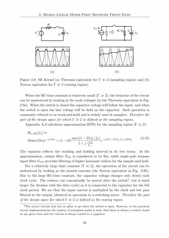
3. Highly-Linear Mixer-First Receiver Front-Ends
Vi
R
CVo
ON OFF ON OFF ON OFF ON OFF
VO
VI
(a)
ON OFF ON OFF ON OFF ON OFF
VO
VI
Vi / RC
Vo
R / D
(b)
Figure 3.9: SE Kernel (a) Thevenin equivalent for Γ 2 (sampling region) and (b)
Norton equivalent for Γ 2 (mixing region).
When the RC-time constant is relatively small (Γ 2), the behavior of the circuit
can be understood by looking at the node voltages (in the Thevenin equivalent in Fig.
3.9a). When the switch is closed the capacitor voltage will follow the input, and when
the switch is open the last voltage will be held on the capacitor. Such operation is
commonly referred to as track-and-hold and is widely used in samplers. Therefore the
part of the design space for which Γ 2 is defined as the sampling region.
Appendix A.3 calculates approximation HTFs for the sampling region (Γ 2):
Hn,SE(fo) ≈
Dsinc(Dn)e−jπDn + (1−D)sinc((1−D)fo/fs)
1 + j−nfsfrc
e−jπ[(1−D)fo/fs+2Dn].(3.12)
The equation reflects the tracking and holding interval in its two terms. In the
approximation, output filter PSE is considered to be flat, while single-pole lowpass
input filter GSE provides filtering of higher harmonic indices for the sample-and-hold.
For a relatively large time constant (Γ 2), the operation of the circuit can be
understood by looking at the branch currents (the Norton equivalent in Fig. 3.9b).
Due to the large RC-time constant, the capacitor voltage changes only slowly each
clock cycle. The resistor can conceptually be moved after the switch2, but is sized
larger (by division with the duty cycle) as it is connected to the capacitor for the full
clock period. We see that the input current is multiplied by the clock and low pass
filtered at the output, identical in operation to a switching mixer. Therefore the part
of the design space for which Γ 2 is defined as the mixing region.
2The source current now has no place to go when the switch is open. However, in the practical
circuit implementations the number of polyphase paths is such, that there is always a switch closed
at any given time and the current is always routed to a capacitor.
42
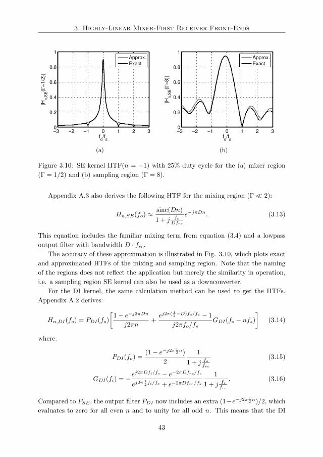
3. Highly-Linear Mixer-First Receiver Front-Ends
−3 −2 −1 0 1 2 30
0.2
0.4
0.6
0.8
1
|Hn,S
E(Γ
=1/2
)|
fo/f
s
Approx.
Exact
(a)
−3 −2 −1 0 1 2 30
0.2
0.4
0.6
0.8
1
|Hn,S
E(Γ
=8)|
fo/f
s
Approx.
Exact
(b)
Figure 3.10: SE kernel HTF(n = −1) with 25% duty cycle for the (a) mixer region
(Γ = 1/2) and (b) sampling region (Γ = 8).
Appendix A.3 also derives the following HTF for the mixing region (Γ 2):
Hn,SE(fo) ≈sinc(Dn)
1 + j foDfrc
e−jπDn. (3.13)
This equation includes the familiar mixing term from equation (3.4) and a lowpass
output filter with bandwidth D · frc.The accuracy of these approximation is illustrated in Fig. 3.10, which plots exact
and approximated HTFs of the mixing and sampling region. Note that the naming
of the regions does not reflect the application but merely the similarity in operation,
i.e. a sampling region SE kernel can also be used as a downconverter.
For the DI kernel, the same calculation method can be used to get the HTFs.
Appendix A.2 derives:
Hn,DI(fo) = PDI(fo)
[1− e−j2πDn
j2πn+ej2π( 1
2−D)fo/fs − 1
j2πfo/fsGDI(fo − nfs)
](3.14)
where:
PDI(fo) =(1− e−j2π 1
2n)
2
1
1 + j fofrc
(3.15)
GDI(fi) = −ej2πDfi/fs − e−2πDfrc/fs
ej2π12 fi/fs + e−2πDfrc/fs
1
1 + j fifrc
. (3.16)
Compared to PSE , the output filter PDI now includes an extra (1−e−j2π 12n)/2, which
evaluates to zero for all even n and to unity for all odd n. This means that the DI
43
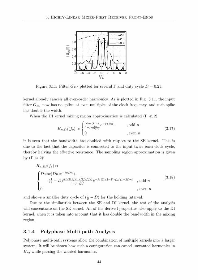
3. Highly-Linear Mixer-First Receiver Front-Ends
−8 −6 −4 −2 0 2 4 6 80
0.2
0.4
0.6
0.8
1
fi/f
s
| G
DI(f
i) |
Γ=20
Γ=2.0
Γ=0.2
Figure 3.11: Filter GDI plotted for several Γ and duty cycle D = 0.25.
kernel already cancels all even-order harmonics. As is plotted in Fig. 3.11, the input
filter GDI now has no spikes at even multiples of the clock frequency, and each spike
has double the width.
When the DI kernel mixing region approximation is calculated (Γ 2):
Hn,DI(fo) ≈
sinc(Dn)
1+j fo2Dfrc
e−jπDn. , odd n
0 , even n(3.17)
it is seen that the bandwidth has doubled with respect to the SE kernel. This is
due to the fact that the capacitor is connected to the input twice each clock cycle,
thereby halving the effective resistance. The sampling region approximation is given
by (Γ 2):
Hn,DI(fo) ≈Dsinc(Dn)e−jπDn+
( 12 −D) sinc((1/2−D)fo/fs)
1+j−nfsfrc
e−jπ[(1/2−D)fo/fs+2Dn] , odd n
0 , even n
(3.18)
and shows a smaller duty cycle of ( 12 −D) for the holding interval.
Due to the similarities between the SE and DI kernel, the rest of the analysis
will concentrate on the SE kernel. All of the derived properties also apply to the DI
kernel, when it is taken into account that it has double the bandwidth in the mixing
region.
3.1.4 Polyphase Multi-path Analysis
Polyphase multi-path systems allow the combination of multiple kernels into a larger
system. It will be shown how such a configuration can cancel unwanted harmonics in
Hn, while passing the wanted harmonics.
44
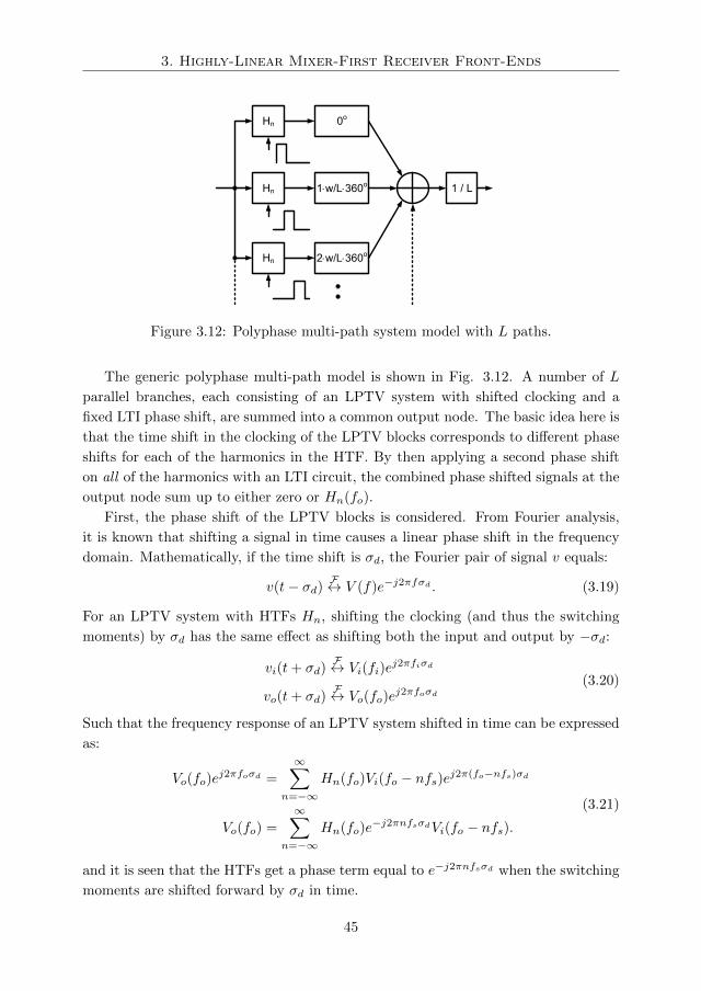
3. Highly-Linear Mixer-First Receiver Front-Ends
Hn
1 / L Hn
Hn 2×w/L×360o
1×w/L×360o
0o
Figure 3.12: Polyphase multi-path system model with L paths.
The generic polyphase multi-path model is shown in Fig. 3.12. A number of L
parallel branches, each consisting of an LPTV system with shifted clocking and a
fixed LTI phase shift, are summed into a common output node. The basic idea here is
that the time shift in the clocking of the LPTV blocks corresponds to different phase
shifts for each of the harmonics in the HTF. By then applying a second phase shift
on all of the harmonics with an LTI circuit, the combined phase shifted signals at the
output node sum up to either zero or Hn(fo).
First, the phase shift of the LPTV blocks is considered. From Fourier analysis,
it is known that shifting a signal in time causes a linear phase shift in the frequency
domain. Mathematically, if the time shift is σd, the Fourier pair of signal v equals:
v(t− σd)F↔ V (f)e−j2πfσd . (3.19)
For an LPTV system with HTFs Hn, shifting the clocking (and thus the switching
moments) by σd has the same effect as shifting both the input and output by −σd:
vi(t+ σd)F↔ Vi(fi)e
j2πfiσd
vo(t+ σd)F↔ Vo(fo)e
j2πfoσd(3.20)
Such that the frequency response of an LPTV system shifted in time can be expressed
as:
Vo(fo)ej2πfoσd =
∞∑n=−∞
Hn(fo)Vi(fo − nfs)ej2π(fo−nfs)σd
Vo(fo) =
∞∑n=−∞
Hn(fo)e−j2πnfsσdVi(fo − nfs).
(3.21)
and it is seen that the HTFs get a phase term equal to e−j2πnfsσd when the switching
moments are shifted forward by σd in time.
45
3. Highly-Linear Mixer-First Receiver Front-Ends
For the polyphase multi-path system, it was defined that the parallel branches are
switched by a polyphase clock, with clock phases that are distributed uniformly across
the clock period. In other words: the l-th path has a clock shifted by σd = l/L · Ts,resulting in a phase shift of −n · l · 360/L.
Next, the LTI phase shift is applied, adding a phase shift of l · w · 360/L for
the l-th path. The w parameter indicates the harmonic index of the first uncanceled
harmonic (provided that w < L), as will be shown shortly. Each path now has the
total phase term:
e−j2πnl/Lej2πwl/L = e−j2π(n−w)l/L. (3.22)
Summing the signals over all paths gives the HTFs of the total system:
Hn,polyphase(fo) =1
L·L−1∑l=0
Hn(fo)e−j2π(n−w)l/L
=
0 , n−wL 6= integer
Hn(fo) , n−wL = integer.
(3.23)
In other words, a polyphase multi-path system passes all frequency shifts with a
harmonic index that satisfies:
n = i · L+ w where i = ...,−2,−1, 0, 1, 2, ... (3.24)
while the transfer functions for all other frequency shifts are zero. Indeed, the first
uncanceled harmonic is the one with index w. For example, with L = 2 and w = −1,
this results in cancellation for all n = ...,−2, 0, 2, .... It can also be seen that for
more than two paths (L > 2), either n or −n (or both) are canceled, automatically
resulting in image rejection.
Two familiar examples of a polyphase system are the differential mixer in Fig.
3.13a and the Hartley image rejection mixer in Fig. 3.13b 3. The scaling factor of
1/L in Fig. 3.12 is a normalization factor, and might not always be present, but
its absence will not modify the fundamental harmonic canceling properties of the
multi-path polyphase system.
3.1.5 Noise
Up to this point, the analysis has been concerned with the transfer function of de-
terministic signals. Of additional interest is the behavior of these LPTV systems
3 In an image-reject receiver the I and Q outputs are usually digitized separately and summed in
the digital domain. Compared to analog summing, the resulting fundamental system image rejection
is equivalent.
46
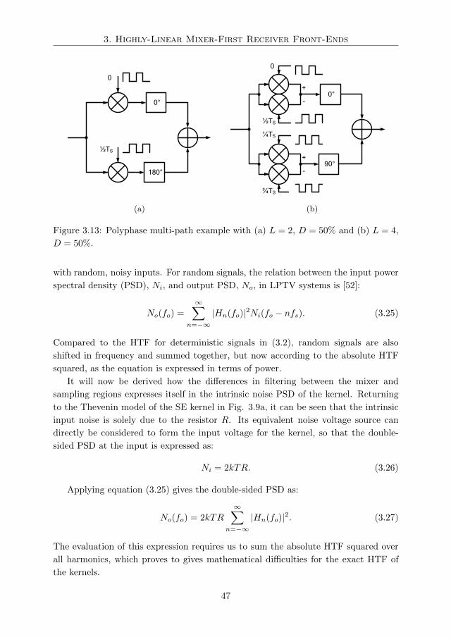
3. Highly-Linear Mixer-First Receiver Front-Ends
0°
180°
0
½TS
(a)
0°
90°
¾TS
¼TS
½TS
0
+
-
+
-
(b)
Figure 3.13: Polyphase multi-path example with (a) L = 2, D = 50% and (b) L = 4,
D = 50%.
with random, noisy inputs. For random signals, the relation between the input power
spectral density (PSD), Ni, and output PSD, No, in LPTV systems is [52]:
No(fo) =
∞∑n=−∞
|Hn(fo)|2Ni(fo − nfs). (3.25)
Compared to the HTF for deterministic signals in (3.2), random signals are also
shifted in frequency and summed together, but now according to the absolute HTF
squared, as the equation is expressed in terms of power.
It will now be derived how the differences in filtering between the mixer and
sampling regions expresses itself in the intrinsic noise PSD of the kernel. Returning
to the Thevenin model of the SE kernel in Fig. 3.9a, it can be seen that the intrinsic
input noise is solely due to the resistor R. Its equivalent noise voltage source can
directly be considered to form the input voltage for the kernel, so that the double-
sided PSD at the input is expressed as:
Ni = 2kTR. (3.26)
Applying equation (3.25) gives the double-sided PSD as:
No(fo) = 2kTR
∞∑n=−∞
|Hn(fo)|2. (3.27)
The evaluation of this expression requires us to sum the absolute HTF squared over
all harmonics, which proves to gives mathematical difficulties for the exact HTF of
the kernels.
47
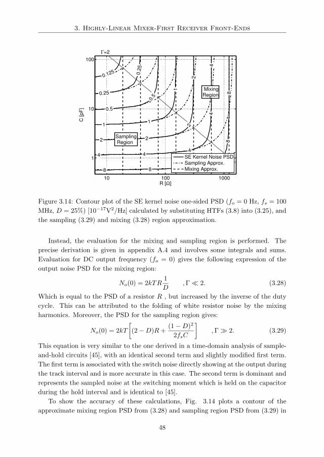
3. Highly-Linear Mixer-First Receiver Front-Ends
10 100 1000
1
10
100
Γ=2
0.125 0.2
5
0.25
0.5
0.5
1
11
22
22
44
444
88
888
Sampling Region
MixingRegion
R [Ω]
C [pF
]
SE Kernel Noise PSD
Sampling Approx.
Mixing Approx.
Figure 3.14: Contour plot of the SE kernel noise one-sided PSD (fo = 0 Hz, fs = 100
MHz, D = 25%) [10−17V2/Hz] calculated by substituting HTFs (3.8) into (3.25), and
the sampling (3.29) and mixing (3.28) region approximation.
Instead, the evaluation for the mixing and sampling region is performed. The
precise derivation is given in appendix A.4 and involves some integrals and sums.
Evaluation for DC output frequency (fo = 0) gives the following expression of the
output noise PSD for the mixing region:
No(0) = 2kTR1
D,Γ 2. (3.28)
Which is equal to the PSD of a resistor R , but increased by the inverse of the duty
cycle. This can be attributed to the folding of white resistor noise by the mixing
harmonics. Moreover, the PSD for the sampling region gives:
No(0) = 2kT
[(2−D)R+
(1−D)2
2fsC
],Γ 2. (3.29)
This equation is very similar to the one derived in a time-domain analysis of sample-
and-hold circuits [45], with an identical second term and slightly modified first term.
The first term is associated with the switch noise directly showing at the output during
the track interval and is more accurate in this case. The second term is dominant and
represents the sampled noise at the switching moment which is held on the capacitor
during the hold interval and is identical to [45].
To show the accuracy of these calculations, Fig. 3.14 plots a contour of the
approximate mixing region PSD from (3.28) and sampling region PSD from (3.29) in
48
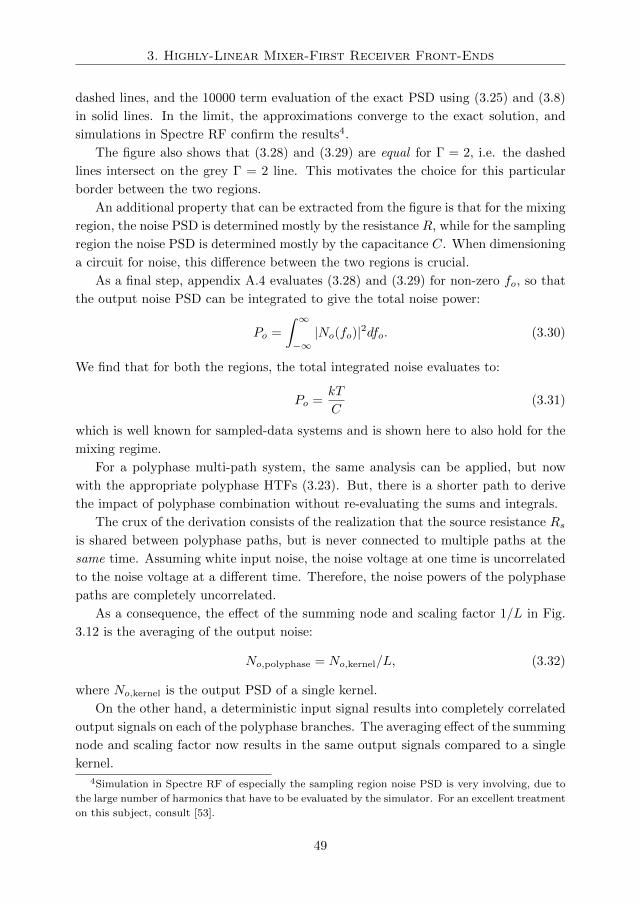
3. Highly-Linear Mixer-First Receiver Front-Ends
dashed lines, and the 10000 term evaluation of the exact PSD using (3.25) and (3.8)
in solid lines. In the limit, the approximations converge to the exact solution, and
simulations in Spectre RF confirm the results4.
The figure also shows that (3.28) and (3.29) are equal for Γ = 2, i.e. the dashed
lines intersect on the grey Γ = 2 line. This motivates the choice for this particular
border between the two regions.
An additional property that can be extracted from the figure is that for the mixing
region, the noise PSD is determined mostly by the resistance R, while for the sampling
region the noise PSD is determined mostly by the capacitance C. When dimensioning
a circuit for noise, this difference between the two regions is crucial.
As a final step, appendix A.4 evaluates (3.28) and (3.29) for non-zero fo, so that
the output noise PSD can be integrated to give the total noise power:
Po =
∫ ∞−∞|No(fo)|2dfo. (3.30)
We find that for both the regions, the total integrated noise evaluates to:
Po =kT
C(3.31)
which is well known for sampled-data systems and is shown here to also hold for the
mixing regime.
For a polyphase multi-path system, the same analysis can be applied, but now
with the appropriate polyphase HTFs (3.23). But, there is a shorter path to derive
the impact of polyphase combination without re-evaluating the sums and integrals.
The crux of the derivation consists of the realization that the source resistance Rsis shared between polyphase paths, but is never connected to multiple paths at the
same time. Assuming white input noise, the noise voltage at one time is uncorrelated
to the noise voltage at a different time. Therefore, the noise powers of the polyphase
paths are completely uncorrelated.
As a consequence, the effect of the summing node and scaling factor 1/L in Fig.
3.12 is the averaging of the output noise:
No,polyphase = No,kernel/L, (3.32)
where No,kernel is the output PSD of a single kernel.
On the other hand, a deterministic input signal results into completely correlated
output signals on each of the polyphase branches. The averaging effect of the summing
node and scaling factor now results in the same output signals compared to a single
kernel.4Simulation in Spectre RF of especially the sampling region noise PSD is very involving, due to
the large number of harmonics that have to be evaluated by the simulator. For an excellent treatment
on this subject, consult [53].
49
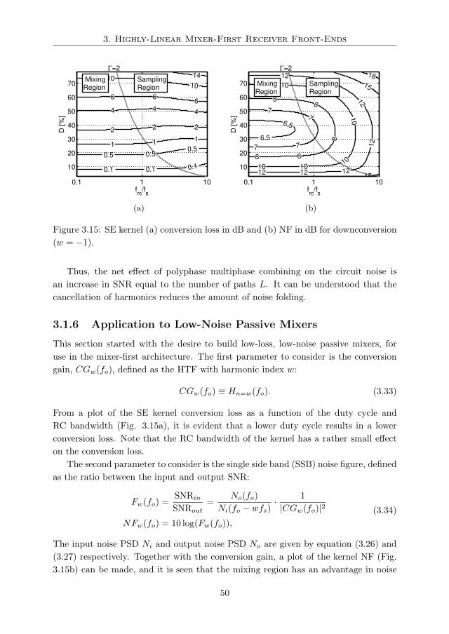
3. Highly-Linear Mixer-First Receiver Front-Ends
0.1 1 10
10
20
30
40
50
60
70
Γ=2
0.1 0.1 0.1
0.5 0.50.5
1 11
2 2 2
4 4 4
6 66
10 1010
14 Mixing Region
Sampling Region
frc
/fs
D [%
]
(a)
0.1 1 10
10
20
30
40
50
60
70
Γ=2
6.5
6.5
77
77
88
8
88
1010
10
101010
1212
12
12
121212
15
15
18 Mixing Region
Sampling Region
frc
/fs
D [%
]
(b)
Figure 3.15: SE kernel (a) conversion loss in dB and (b) NF in dB for downconversion
(w = −1).
Thus, the net effect of polyphase multiphase combining on the circuit noise is
an increase in SNR equal to the number of paths L. It can be understood that the
cancellation of harmonics reduces the amount of noise folding.
3.1.6 Application to Low-Noise Passive Mixers
This section started with the desire to build low-loss, low-noise passive mixers, for
use in the mixer-first architecture. The first parameter to consider is the conversion
gain, CGw(fo), defined as the HTF with harmonic index w:
CGw(fo) ≡ Hn=w(fo). (3.33)
From a plot of the SE kernel conversion loss as a function of the duty cycle and
RC bandwidth (Fig. 3.15a), it is evident that a lower duty cycle results in a lower
conversion loss. Note that the RC bandwidth of the kernel has a rather small effect
on the conversion loss.
The second parameter to consider is the single side band (SSB) noise figure, defined
as the ratio between the input and output SNR:
Fw(fo) =SNRin
SNRout=
No(fo)
Ni(fo − wfs)· 1
|CGw(fo)|2
NFw(fo) = 10 log(Fw(fo)),
(3.34)
The input noise PSD Ni and output noise PSD No are given by equation (3.26) and
(3.27) respectively. Together with the conversion gain, a plot of the kernel NF (Fig.
3.15b) can be made, and it is seen that the mixing region has an advantage in noise
50
3. Highly-Linear Mixer-First Receiver Front-Ends
2 3 4 5 6 7 80
1
2
3
4
5
L=1/D
CL
and N
F [dB
]
Figure 3.16: Mixing region conversion loss and minimum noise figure due to folding.
figure over the sampling region for equal duty cycle. Additionally, there is an optimum
in noise figure a duty cycle of around 37%.
One additional thing must be considered though. The loop resistance R is in
fact the sum of source resistance Rs and switch-on resistance Ron. Only the first
represents the actual input noise, while the second is noise added by the circuit itself.
In the total noise figure, the input noise is therefore a factor of Rs/Rs +Ron smaller.
Applying this to equation (3.34) gives the same expression for the kernel noise
figure as before, but now with an extra factor:
Fw(fo) =
(1 +
RonRs
)︸ ︷︷ ︸
A
·∑∞n=−∞ |Hn(fo)|2
|Hw(fo)|2︸ ︷︷ ︸B
. (3.35)
The A factor is added and corresponds to the Linear Time Invariant (LTI) noise
figure for the SE kernel with closed switch and no periodic switching at all. The B
term represents the noise folding due to the circuit switching, plotted in Fig. 3.15b.
Therefore, for calculating the NF, the LPTV kernel analysis can be done with the
total resistance R and the effect of Ron can be factored in afterwards.
Continuing by considering the results from the polyphase noise analysis, it is found
that the noise figure decreases when the number of polyphase paths is increased. The
limit on the number of paths is the requirement that the clock is non-overlapping, so
for optimum noise figure we have to ”fill the phases”, and set the number of paths L
to:
L =1
D. (3.36)
If we furthermore use the approximate transfer function for the mixing region, the
noise factor can be expressed as:
F =
(1 +
RonRs
)· 1
|sinc(D)|2. (3.37)
51
3. Highly-Linear Mixer-First Receiver Front-Ends
The noise contribution due to the switches can be minimized by lowering the switch-
on resistance5 and the contribution due to the noise folding can be minimized by
decreasing the duty cycle (which increases the number of polyphase paths). As the
conversion los of a single kernel is equal to sinc(D), we find that for zero switch-on
resistance the fundamental minimum conversion gain and minimum noise figure of a
polyphase passive mixer are equal to:
CGkernel[dB] = −NFmin[dB] = −20 · log (sinc(D)) (3.38)
So although a single kernel has on optimum in noise for 37% duty cycle, a completely
filled polyphase system of kernels has lower noise for smaller duty cycles.
Plotting the conversion gain and noise figure for the completely filled polyphase
system in Fig. 3.16, it can be observed that the step from 2 paths and 50% duty
cycle, to 4 paths and 25 % duty cycle delivers a big improvement. Conveniently this
requires four polyphase paths, which can be arranged as a differential In-phase and
Quadrature output for image rejection and vector modulation. The improvements
with a further increase of the number of paths is less pronounced.
To demonstrate the high SFDR of such a mixer-first receiver with a DI kernel, 25%
duty cycle switched-RC mixer, the next section presents a chip design in advanced
CMOS.
3.2 Implementation in 65-nm CMOS
Figure 12.4.2 shows the proposed mixer-first direct conversion architecture with a
4-phase 25% duty cycle differential mixer and feedback amplifiers at IF. A completely
differential design cancels out second order distortions, ensuring that third order
intermodulation harmonics dominate the linearity performance.
3.2.1 Mixer and Feedback Amplifier
The bandwidth BW is set by the DI kernel capacitance:
C =D
πR ·BW. (3.39)
where the BW must be smaller than πD/fs to ensure that the kernel operates in
the mixing region. The resistance for the DI mixer kernel consists of the 5 Ω switch
on-resistance added to the 50 Ω source impedance, which together with 65 pF on-chip
capacitance results in 22 MHz of mixer bandwidth. The switch resistance increases
the mixer NF to 1.9 dB and limits the IIP3 to 26 dBm.
5The switch-off resistance is rarely a limiting factor in practical MOSFET switches.
52
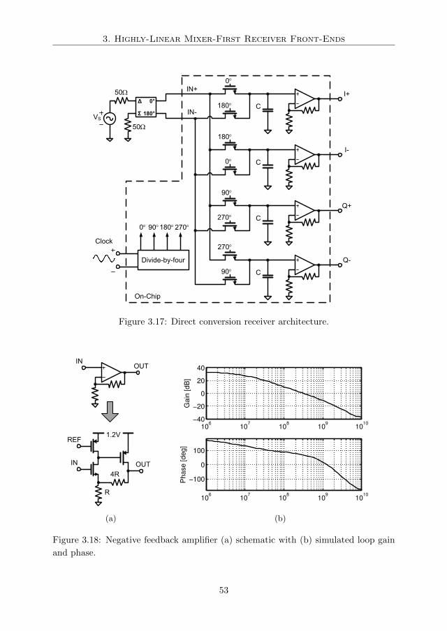
3. Highly-Linear Mixer-First Receiver Front-Ends
Δ
Σ
0°
180°
270°
C90°
Q-
90°
C270°
Q+
180°
C0°
I-
0°
C180°
I+
VS
50W
50W
0° 90°180°270°
On-Chip
IN+
IN-
Clock
Divide-by-four
Figure 3.17: Direct conversion receiver architecture.
INOUT
R
4R
IN OUT
REF1.2V
(a)
106
107
108
109
1010
−40
−20
0
20
40
Gain
[dB
]
106
107
108
109
1010
−100
0
100
Phase [deg]
(b)
Figure 3.18: Negative feedback amplifier (a) schematic with (b) simulated loop gain
and phase.
53
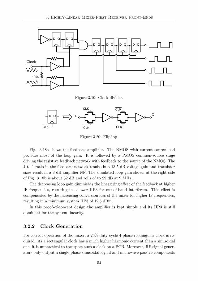
3. Highly-Linear Mixer-First Receiver Front-Ends
100W
D QD Q
Clock
D Q D Q D Q D Q
Figure 3.19: Clock divider.
D Q
CLK
CLK
CLK
CLK
CLK
QD
Figure 3.20: Flipflop.
Fig. 3.18a shows the feedback amplifier. The NMOS with current source load
provides most of the loop gain. It is followed by a PMOS common-source stage
driving the resistive feedback network with feedback to the source of the NMOS. The
4 to 1 ratio in the feedback network results in a 13.5 dB voltage gain and transistor
sizes result in a 3 dB amplifier NF. The simulated loop gain shown at the right side
of Fig. 3.18b is about 32 dB and rolls of to 29 dB at 9 MHz.
The decreasing loop gain diminishes the linearizing effect of the feedback at higher
IF frequencies, resulting in a lower IIP3 for out-of-band interferers. This effect is
compensated by the increasing conversion loss of the mixer for higher IF frequencies,
resulting in a minimum system IIP3 of 12.5 dBm.
In this proof-of-concept design the amplifier is kept simple and its IIP3 is still
dominant for the system linearity.
3.2.2 Clock Generation
For correct operation of the mixer, a 25% duty cycle 4-phase rectangular clock is re-
quired. As a rectangular clock has a much higher harmonic content than a sinusoidal
one, it is unpractical to transport such a clock on a PCB. Moreover, RF signal gener-
ators only output a single-phase sinusoidal signal and microwave passive components
54
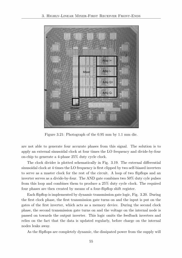
3. Highly-Linear Mixer-First Receiver Front-Ends
Mixer
Amp I+
Amp I-
Amp Q+
Amp Q-
Divider
Figure 3.21: Photograph of the 0.95 mm by 1.1 mm die.
are not able to generate four accurate phases from this signal. The solution is to
apply an external sinusoidal clock at four times the LO frequency and divide-by-four
on-chip to generate a 4-phase 25% duty cycle clock.
The clock divider is plotted schematically in Fig. 3.19. The external differential
sinusoidal clock at 4 times the LO frequency is first clipped by two self-biased inverters
to serve as a master clock for the rest of the circuit. A loop of two flipflops and an
inverter serves as a divide-by-four. The AND gate combines two 50% duty cyle pulses
from this loop and combines them to produce a 25% duty cycle clock. The required
four phases are then created by means of a four-flipflop shift register.
Each flipflop is implemented by dynamic transmission gate logic, Fig. 3.20. During
the first clock phase, the first transmission gate turns on and the input is put on the
gates of the first inverter, which acts as a memory device. During the second clock
phase, the second transmission gate turns on and the voltage on the internal node is
passed on towards the output inverter. This logic omits the feedback inverters and
relies on the fact that the data is updated regularly, before charge on the internal
nodes leaks away.
As the flipflops are completely dynamic, the dissipated power from the supply will
55
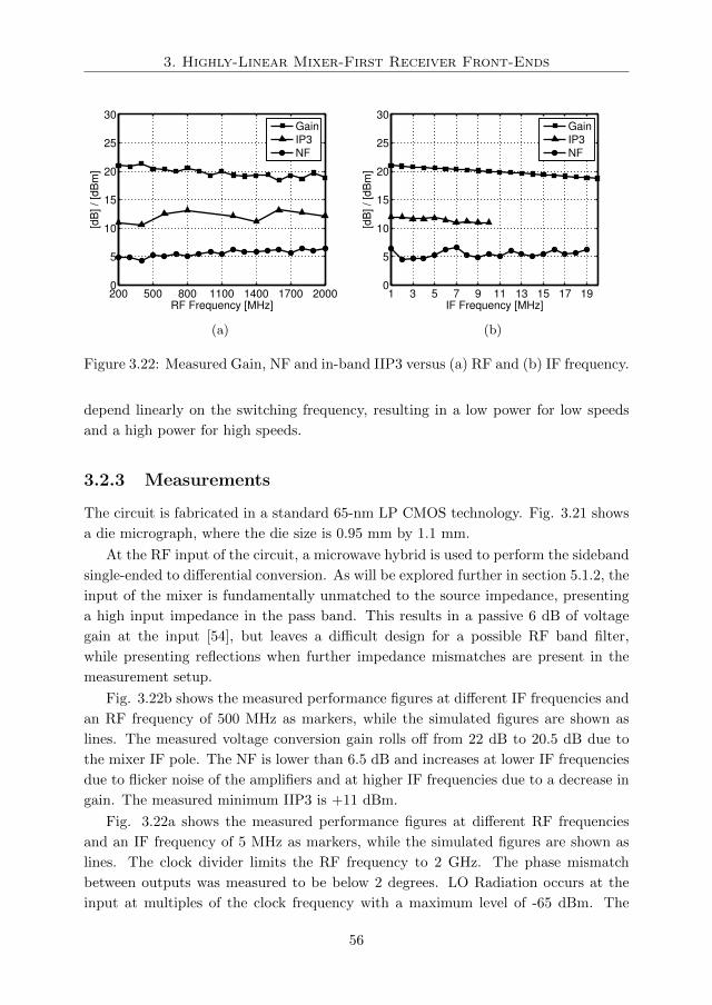
3. Highly-Linear Mixer-First Receiver Front-Ends
200 500 800 1100 1400 1700 20000
5
10
15
20
25
30
RF Frequency [MHz]
[dB
] / [d
Bm
]
Gain
IP3
NF
(a)
1 3 5 7 9 11 13 15 17 190
5
10
15
20
25
30
IF Frequency [MHz]
[dB
] / [d
Bm
]
Gain
IP3
NF
(b)
Figure 3.22: Measured Gain, NF and in-band IIP3 versus (a) RF and (b) IF frequency.
depend linearly on the switching frequency, resulting in a low power for low speeds
and a high power for high speeds.
3.2.3 Measurements
The circuit is fabricated in a standard 65-nm LP CMOS technology. Fig. 3.21 shows
a die micrograph, where the die size is 0.95 mm by 1.1 mm.
At the RF input of the circuit, a microwave hybrid is used to perform the sideband
single-ended to differential conversion. As will be explored further in section 5.1.2, the
input of the mixer is fundamentally unmatched to the source impedance, presenting
a high input impedance in the pass band. This results in a passive 6 dB of voltage
gain at the input [54], but leaves a difficult design for a possible RF band filter,
while presenting reflections when further impedance mismatches are present in the
measurement setup.
Fig. 3.22b shows the measured performance figures at different IF frequencies and
an RF frequency of 500 MHz as markers, while the simulated figures are shown as
lines. The measured voltage conversion gain rolls off from 22 dB to 20.5 dB due to
the mixer IF pole. The NF is lower than 6.5 dB and increases at lower IF frequencies
due to flicker noise of the amplifiers and at higher IF frequencies due to a decrease in
gain. The measured minimum IIP3 is +11 dBm.
Fig. 3.22a shows the measured performance figures at different RF frequencies
and an IF frequency of 5 MHz as markers, while the simulated figures are shown as
lines. The clock divider limits the RF frequency to 2 GHz. The phase mismatch
between outputs was measured to be below 2 degrees. LO Radiation occurs at the
input at multiples of the clock frequency with a maximum level of -65 dBm. The
56
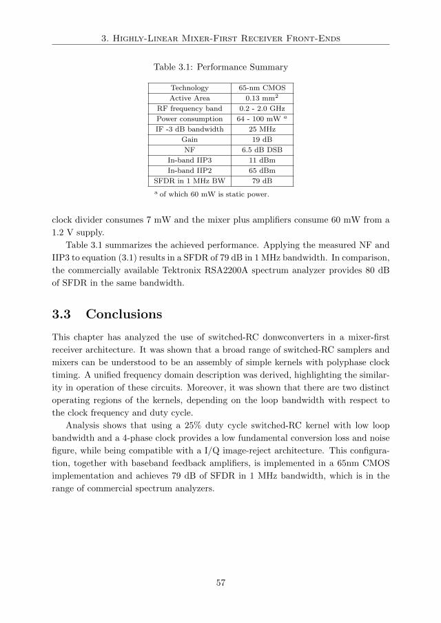
3. Highly-Linear Mixer-First Receiver Front-Ends
Table 3.1: Performance Summary
Technology 65-nm CMOS
Active Area 0.13 mm2
RF frequency band 0.2 - 2.0 GHz
Power consumption 64 - 100 mW a
IF -3 dB bandwidth 25 MHz
Gain 19 dB
NF 6.5 dB DSB
In-band IIP3 11 dBm
In-band IIP2 65 dBm
SFDR in 1 MHz BW 79 dB
a of which 60 mW is static power.
clock divider consumes 7 mW and the mixer plus amplifiers consume 60 mW from a
1.2 V supply.
Table 3.1 summarizes the achieved performance. Applying the measured NF and
IIP3 to equation (3.1) results in a SFDR of 79 dB in 1 MHz bandwidth. In comparison,
the commercially available Tektronix RSA2200A spectrum analyzer provides 80 dB
of SFDR in the same bandwidth.
3.3 Conclusions
This chapter has analyzed the use of switched-RC donwconverters in a mixer-first
receiver architecture. It was shown that a broad range of switched-RC samplers and
mixers can be understood to be an assembly of simple kernels with polyphase clock
timing. A unified frequency domain description was derived, highlighting the similar-
ity in operation of these circuits. Moreover, it was shown that there are two distinct
operating regions of the kernels, depending on the loop bandwidth with respect to
the clock frequency and duty cycle.
Analysis shows that using a 25% duty cycle switched-RC kernel with low loop
bandwidth and a 4-phase clock provides a low fundamental conversion loss and noise
figure, while being compatible with a I/Q image-reject architecture. This configura-
tion, together with baseband feedback amplifiers, is implemented in a 65nm CMOS
implementation and achieves 79 dB of SFDR in 1 MHz bandwidth, which is in the
range of commercial spectrum analyzers.
57
Chapter 4
Approximate-Sine Vector
Modulator Beamforming
In the previous chapter, the highly linear mixer-first architecture with passive mix-
ing has been introduced to serve as a downconverting front-end. In phased arrays,
the key additional component to be considered is the phase shifter, which function
is to align the incoming antenna signals in phase. For this circuit, additional design
trade-offs besides spurious free dynamic range need to be made, such as phase shift
resolution, amplitude error and frequency range. A straight-forward design approach
that uses classical filter design to build the correct phase response can be unpracti-
cal for CMOS integration, due to the poor integration of coils on-chip and limited
operating frequency of active filters.
Alternatively, different ways of producing a phase shift have been introduced, such
as injection locking [55], LO phase selection [56] and vector modulation [57][25][19].
Each approach has its own strengths and weaknesses, but they all share the property
that signals are processed in the continuous-time domain. With CMOS technology
being optimized for digital processing, which takes place in the discrete-time domain,
there is potentially a lot to be gained in implementing discrete-time phase shifters.
To this end, this chapter presents a phased-array architecture based on a switched-
capacitor vector modulator that operates in the discrete-time domain.
4.1 Switched-Capacitor Phase Shifter
In this section we will introduce the vector modulator for performing the phase shift
and amplitude control in a phased array, and show how it can be implemented with
switched-capacitor circuits.
58
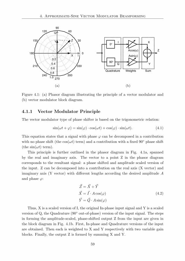
4. Approximate-Sine Vector Modulator Beamforming
0.2
0.4
0.6
0.8
1.0
30
210
60
240
90
270
120
300
150
330
180 0
Z
X
Y
I
Q
(a)
0°
90°
I
Q
X
Y
Acos(j)
Asin(j)
Quadrature Weights Sum
Z
(b)
Figure 4.1: (a) Phasor diagram illustrating the principle of a vector modulator and
(b) vector modulator block diagram.
4.1.1 Vector Modulator Principle
The vector modulator type of phase shifter is based on the trigonometric relation:
sin(ωt+ ϕ) = sin(ϕ) · cos(ωt) + cos(ϕ) · sin(ωt). (4.1)
This equation states that a signal with phase ϕ can be decomposed in a contribution
with no phase shift (the cos(ωt) term) and a contribution with a fixed 90 phase shift
(the sin(ωt) term).
This principle is further outlined in the phasor diagram in Fig. 4.1a, spanned
by the real and imaginary axis. The vector to a point Z in the phasor diagram
corresponds to the resultant signal: a phase shifted and amplitude scaled version of
the input. Z can be decomposed into a contribution on the real axis (X vector) and
imaginary axis (Y vector) with different lengths according the desired amplitude A
and phase ϕ:
~Z = ~X + ~Y
~X = ~I ·A cos(ϕ)
~Y = ~Q ·A sin(ϕ)
(4.2)
Thus, X is a scaled version of I, the original In-phase input signal and Y is a scaled
version of Q, the Quadrature (90 out-of-phase) version of the input signal. The steps
in forming the amplitude-scaled, phase-shifted output Z from the input are given in
the block diagram in Fig. 4.1b. First, In-phase and Quadrature versions of the input
are obtained. Then each is weighted to X and Y respectively with two variable gain
blocks. Finally, the output Z is formed by summing X and Y.
59
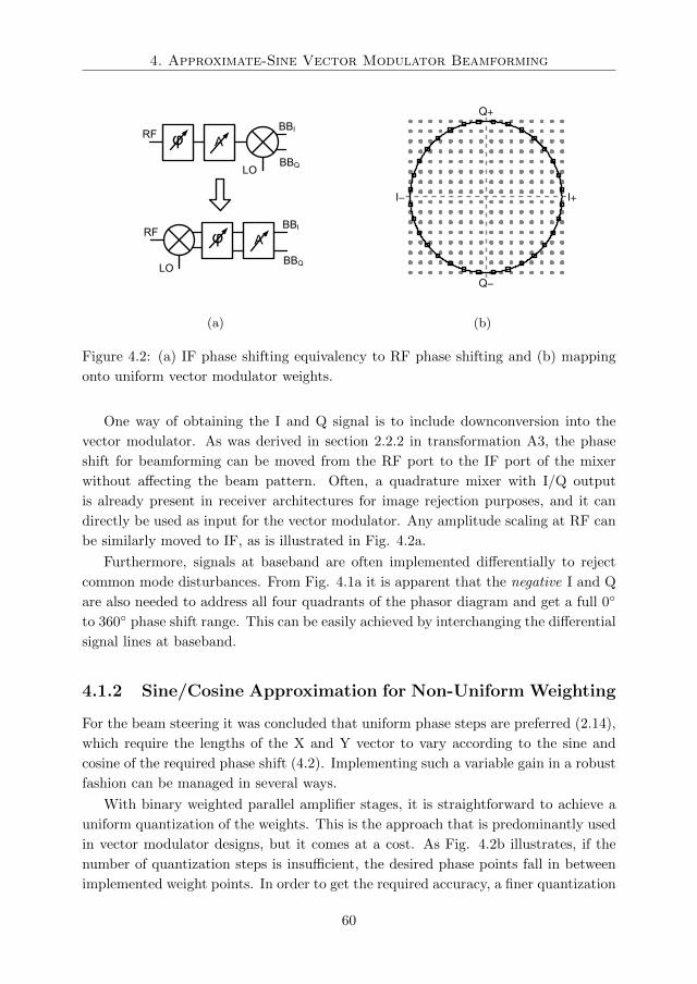
4. Approximate-Sine Vector Modulator Beamforming
AφBBI
RF
LO
AφBBI
BBQ
RF
LO
BBQ
(a)
I− I+
Q−
Q+
(b)
Figure 4.2: (a) IF phase shifting equivalency to RF phase shifting and (b) mapping
onto uniform vector modulator weights.
One way of obtaining the I and Q signal is to include downconversion into the
vector modulator. As was derived in section 2.2.2 in transformation A3, the phase
shift for beamforming can be moved from the RF port to the IF port of the mixer
without affecting the beam pattern. Often, a quadrature mixer with I/Q output
is already present in receiver architectures for image rejection purposes, and it can
directly be used as input for the vector modulator. Any amplitude scaling at RF can
be similarly moved to IF, as is illustrated in Fig. 4.2a.
Furthermore, signals at baseband are often implemented differentially to reject
common mode disturbances. From Fig. 4.1a it is apparent that the negative I and Q
are also needed to address all four quadrants of the phasor diagram and get a full 0
to 360 phase shift range. This can be easily achieved by interchanging the differential
signal lines at baseband.
4.1.2 Sine/Cosine Approximation for Non-Uniform Weighting
For the beam steering it was concluded that uniform phase steps are preferred (2.14),
which require the lengths of the X and Y vector to vary according to the sine and
cosine of the required phase shift (4.2). Implementing such a variable gain in a robust
fashion can be managed in several ways.
With binary weighted parallel amplifier stages, it is straightforward to achieve a
uniform quantization of the weights. This is the approach that is predominantly used
in vector modulator designs, but it comes at a cost. As Fig. 4.2b illustrates, if the
number of quantization steps is insufficient, the desired phase points fall in between
implemented weight points. In order to get the required accuracy, a finer quantization
60
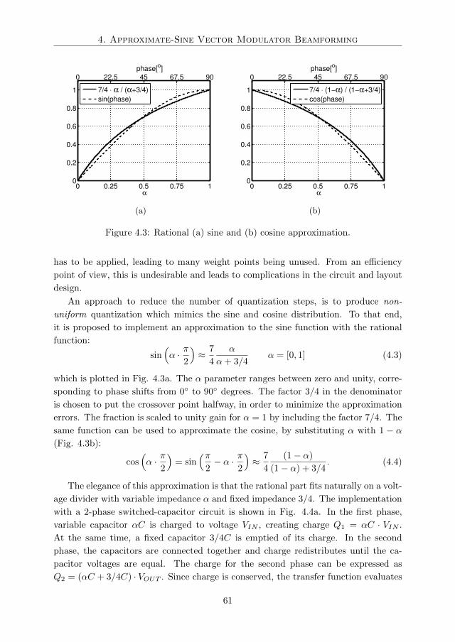
4. Approximate-Sine Vector Modulator Beamforming
0 0.25 0.5 0.75 10
0.2
0.4
0.6
0.8
1
0 22.5 45 67.5 90
α
phase[o]
7/4 ⋅ α / (α+3/4)
sin(phase)
(a)
0 0.25 0.5 0.75 10
0.2
0.4
0.6
0.8
1
0 22.5 45 67.5 90
α
phase[o]
7/4 ⋅ (1−α) / (1−α+3/4)
cos(phase)
(b)
Figure 4.3: Rational (a) sine and (b) cosine approximation.
has to be applied, leading to many weight points being unused. From an efficiency
point of view, this is undesirable and leads to complications in the circuit and layout
design.
An approach to reduce the number of quantization steps, is to produce non-
uniform quantization which mimics the sine and cosine distribution. To that end,
it is proposed to implement an approximation to the sine function with the rational
function:
sin(α · π
2
)≈ 7
4
α
α+ 3/4α = [0, 1] (4.3)
which is plotted in Fig. 4.3a. The α parameter ranges between zero and unity, corre-
sponding to phase shifts from 0 to 90 degrees. The factor 3/4 in the denominator
is chosen to put the crossover point halfway, in order to minimize the approximation
errors. The fraction is scaled to unity gain for α = 1 by including the factor 7/4. The
same function can be used to approximate the cosine, by substituting α with 1 − α(Fig. 4.3b):
cos(α · π
2
)= sin
(π2− α · π
2
)≈ 7
4
(1− α)
(1− α) + 3/4. (4.4)
The elegance of this approximation is that the rational part fits naturally on a volt-
age divider with variable impedance α and fixed impedance 3/4. The implementation
with a 2-phase switched-capacitor circuit is shown in Fig. 4.4a. In the first phase,
variable capacitor αC is charged to voltage VIN , creating charge Q1 = αC · VIN .
At the same time, a fixed capacitor 3/4C is emptied of its charge. In the second
phase, the capacitors are connected together and charge redistributes until the ca-
pacitor voltages are equal. The charge for the second phase can be expressed as
Q2 = (αC + 3/4C) · VOUT . Since charge is conserved, the transfer function evaluates
61
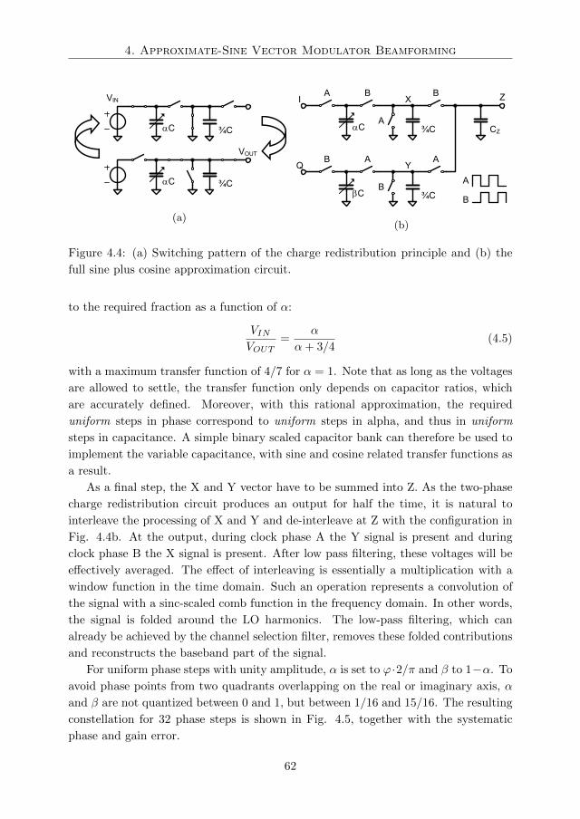
4. Approximate-Sine Vector Modulator Beamforming
aC ¾C
VOUT
aC ¾C
VIN
(a)
aC ¾C
I
bC ¾C
Q
CZ
ZX
Y
A
B
A B B
A
B A A
B
(b)
Figure 4.4: (a) Switching pattern of the charge redistribution principle and (b) the
full sine plus cosine approximation circuit.
to the required fraction as a function of α:
VINVOUT
=α
α+ 3/4(4.5)
with a maximum transfer function of 4/7 for α = 1. Note that as long as the voltages
are allowed to settle, the transfer function only depends on capacitor ratios, which
are accurately defined. Moreover, with this rational approximation, the required
uniform steps in phase correspond to uniform steps in alpha, and thus in uniform
steps in capacitance. A simple binary scaled capacitor bank can therefore be used to
implement the variable capacitance, with sine and cosine related transfer functions as
a result.
As a final step, the X and Y vector have to be summed into Z. As the two-phase
charge redistribution circuit produces an output for half the time, it is natural to
interleave the processing of X and Y and de-interleave at Z with the configuration in
Fig. 4.4b. At the output, during clock phase A the Y signal is present and during
clock phase B the X signal is present. After low pass filtering, these voltages will be
effectively averaged. The effect of interleaving is essentially a multiplication with a
window function in the time domain. Such an operation represents a convolution of
the signal with a sinc-scaled comb function in the frequency domain. In other words,
the signal is folded around the LO harmonics. The low-pass filtering, which can
already be achieved by the channel selection filter, removes these folded contributions
and reconstructs the baseband part of the signal.
For uniform phase steps with unity amplitude, α is set to ϕ·2/π and β to 1−α. To
avoid phase points from two quadrants overlapping on the real or imaginary axis, α
and β are not quantized between 0 and 1, but between 1/16 and 15/16. The resulting
constellation for 32 phase steps is shown in Fig. 4.5, together with the systematic
phase and gain error.
62
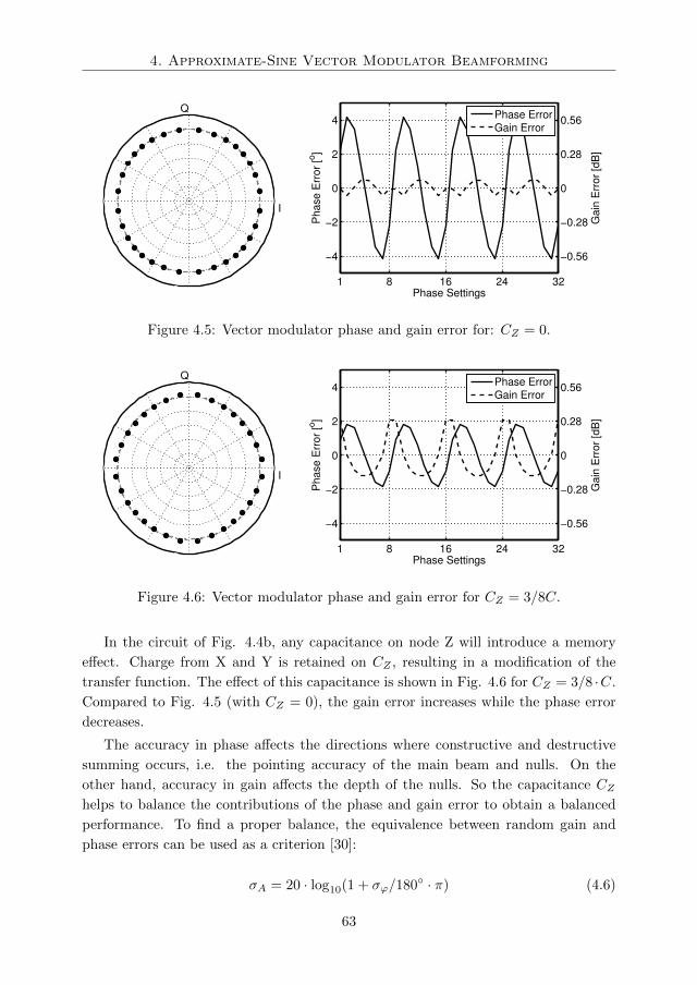
4. Approximate-Sine Vector Modulator Beamforming
0.2
0.4
0.6
0.8
1.0
1.2
30
210
60
240
90
270
120
300
150
330
180 0I
Q
1 8 16 24 32
−4
−2
0
2
4
Phase Settings
Ph
ase E
rror
[o]
−0.56
−0.28
0
0.28
0.56
Gain
Err
or
[dB
]
Phase Error
Gain Error
Figure 4.5: Vector modulator phase and gain error for: CZ = 0.
0.2
0.4
0.6
0.8
1.0
1.2
30
210
60
240
90
270
120
300
150
330
180 0I
Q
1 8 16 24 32
−4
−2
0
2
4
Phase Settings
Pha
se E
rro
r [o
]
−0.56
−0.28
0
0.28
0.56
Ga
in E
rro
r [d
B]
Phase Error
Gain Error
Figure 4.6: Vector modulator phase and gain error for CZ = 3/8C.
In the circuit of Fig. 4.4b, any capacitance on node Z will introduce a memory
effect. Charge from X and Y is retained on CZ , resulting in a modification of the
transfer function. The effect of this capacitance is shown in Fig. 4.6 for CZ = 3/8 ·C.
Compared to Fig. 4.5 (with CZ = 0), the gain error increases while the phase error
decreases.
The accuracy in phase affects the directions where constructive and destructive
summing occurs, i.e. the pointing accuracy of the main beam and nulls. On the
other hand, accuracy in gain affects the depth of the nulls. So the capacitance CZhelps to balance the contributions of the phase and gain error to obtain a balanced
performance. To find a proper balance, the equivalence between random gain and
phase errors can be used as a criterion [30]:
σA = 20 · log10(1 + σϕ/180 · π) (4.6)
63
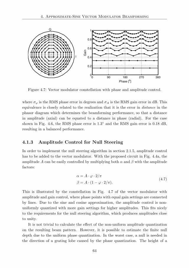
4. Approximate-Sine Vector Modulator Beamforming
I
Q
0 90 180 270 3600
0.2
0.4
0.6
0.8
1
Phase [o]
Gain
Figure 4.7: Vector modulator constellation with phase and amplitude control.
where σϕ is the RMS phase error in degrees and σA is the RMS gain error in dB. This
equivalence is closely related to the realization that it is the error in distance in the
phasor diagram which determines the beamforming performance, so that a distance
in amplitude (axial) can be equated to a distance in phase (radial). For the case
shown in Fig. 4.6, the RMS phase error is 1.3 and the RMS gain error is 0.18 dB,
resulting in a balanced performance.
4.1.3 Amplitude Control for Null Steering
In order to implement the null steering algorithm in section 2.1.5, amplitude control
has to be added to the vector modulator. With the proposed circuit in Fig. 4.4a, the
amplitude A can be easily controlled by multiplying both α and β with the amplitude
factors:
α = A · ϕ · 2/πβ = A · (1− ϕ · 2/π).
(4.7)
This is illustrated by the constellation in Fig. 4.7 of the vector modulator with
amplitude and gain control, where phase points with equal gain settings are connected
by lines. Due to the sine and cosine approximation, the amplitude control is non-
uniformly quantized with more gain settings for higher amplitudes. This fits nicely
to the requirements for the null steering algorithm, which produces amplitudes close
to unity.
It is not trivial to calculate the effect of the non-uniform amplitude quantization
on the resulting beam pattern. However, it is possible to estimate the finite null
depth due to the uniform phase quantization. In the worst case, a null is needed in
the direction of a grating lobe caused by the phase quantization. The height of a
64
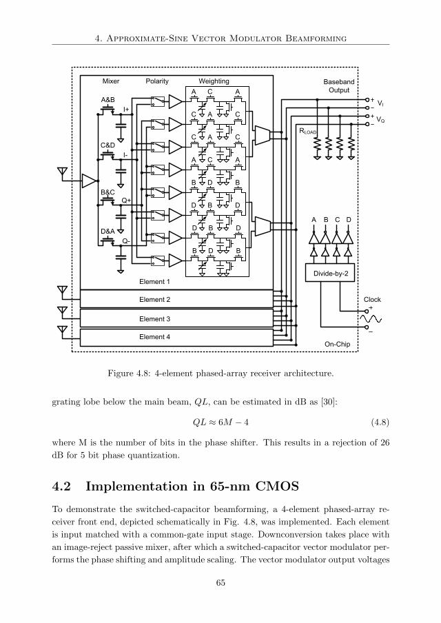
4. Approximate-Sine Vector Modulator Beamforming
I+VI
VQ
Baseband
Output
BA C D
Clock
On-Chip
Element 1
Divide-by-2
A&B
C&D
B&C
D&A
RLOAD
Element 2
Element 3
Element 4
I-
Q+
Q-
C A C
A C A
C A C
A C A
B D B
B D B
D B D
D B D
Polarity WeightingMixer
Figure 4.8: 4-element phased-array receiver architecture.
grating lobe below the main beam, QL, can be estimated in dB as [30]:
QL ≈ 6M − 4 (4.8)
where M is the number of bits in the phase shifter. This results in a rejection of 26
dB for 5 bit phase quantization.
4.2 Implementation in 65-nm CMOS
To demonstrate the switched-capacitor beamforming, a 4-element phased-array re-
ceiver front end, depicted schematically in Fig. 4.8, was implemented. Each element
is input matched with a common-gate input stage. Downconversion takes place with
an image-reject passive mixer, after which a switched-capacitor vector modulator per-
forms the phase shifting and amplitude scaling. The vector modulator output voltages
65
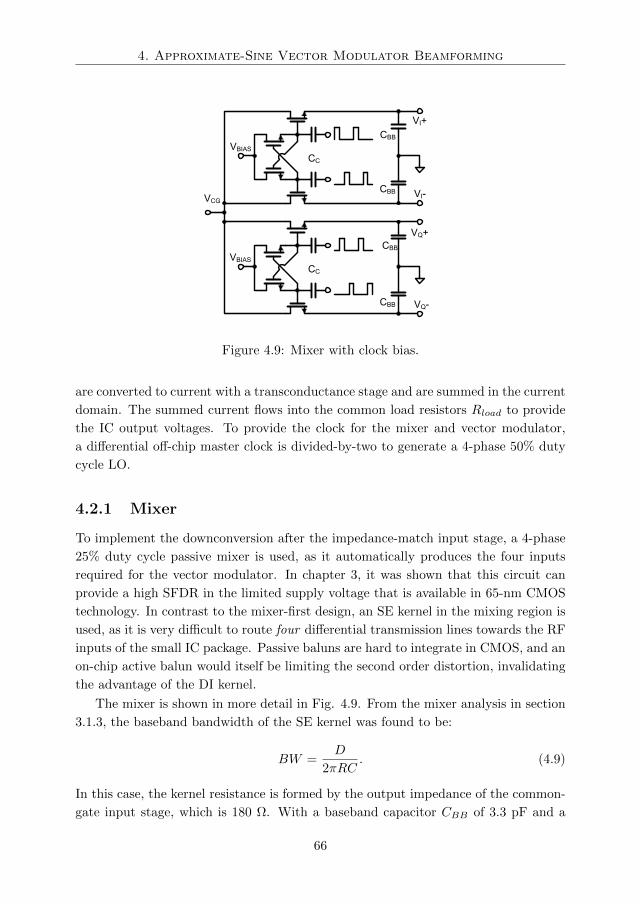
4. Approximate-Sine Vector Modulator Beamforming
CBB
CBB
CC
VBIAS
VQ+
VQ-
CBB
CBB
CC
VBIAS
VI+
VI-VCG
Figure 4.9: Mixer with clock bias.
are converted to current with a transconductance stage and are summed in the current
domain. The summed current flows into the common load resistors Rload to provide
the IC output voltages. To provide the clock for the mixer and vector modulator,
a differential off-chip master clock is divided-by-two to generate a 4-phase 50% duty
cycle LO.
4.2.1 Mixer
To implement the downconversion after the impedance-match input stage, a 4-phase
25% duty cycle passive mixer is used, as it automatically produces the four inputs
required for the vector modulator. In chapter 3, it was shown that this circuit can
provide a high SFDR in the limited supply voltage that is available in 65-nm CMOS
technology. In contrast to the mixer-first design, an SE kernel in the mixing region is
used, as it is very difficult to route four differential transmission lines towards the RF
inputs of the small IC package. Passive baluns are hard to integrate in CMOS, and an
on-chip active balun would itself be limiting the second order distortion, invalidating
the advantage of the DI kernel.
The mixer is shown in more detail in Fig. 4.9. From the mixer analysis in section
3.1.3, the baseband bandwidth of the SE kernel was found to be:
BW =D
2πRC. (4.9)
In this case, the kernel resistance is formed by the output impedance of the common-
gate input stage, which is 180 Ω. With a baseband capacitor CBB of 3.3 pF and a
66
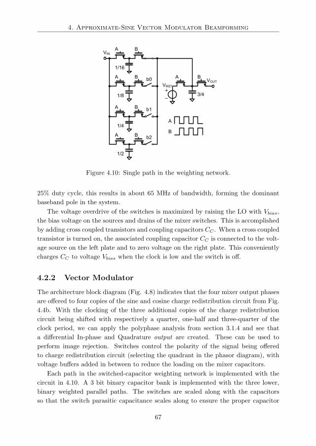
4. Approximate-Sine Vector Modulator Beamforming
A
1/16
B
A
1/8
Bb0
A
1/4
Bb1
A
1/2
Bb2
VIN
A
3/4
B
VRSTVOUT
A
B
Figure 4.10: Single path in the weighting network.
25% duty cycle, this results in about 65 MHz of bandwidth, forming the dominant
baseband pole in the system.
The voltage overdrive of the switches is maximized by raising the LO with Vbias,
the bias voltage on the sources and drains of the mixer switches. This is accomplished
by adding cross coupled transistors and coupling capacitors CC . When a cross coupled
transistor is turned on, the associated coupling capacitor CC is connected to the volt-
age source on the left plate and to zero voltage on the right plate. This conveniently
charges CC to voltage Vbias when the clock is low and the switch is off.
4.2.2 Vector Modulator
The architecture block diagram (Fig. 4.8) indicates that the four mixer output phases
are offered to four copies of the sine and cosine charge redistribution circuit from Fig.
4.4b. With the clocking of the three additional copies of the charge redistribution
circuit being shifted with respectively a quarter, one-half and three-quarter of the
clock period, we can apply the polyphase analysis from section 3.1.4 and see that
a differential In-phase and Quadrature output are created. These can be used to
perform image rejection. Switches control the polarity of the signal being offered
to charge redistribution circuit (selecting the quadrant in the phasor diagram), with
voltage buffers added in between to reduce the loading on the mixer capacitors.
Each path in the switched-capacitor weighting network is implemented with the
circuit in 4.10. A 3 bit binary capacitor bank is implemented with the three lower,
binary weighted parallel paths. The switches are scaled along with the capacitors
so that the switch parasitic capacitance scales along to ensure the proper capacitor
67
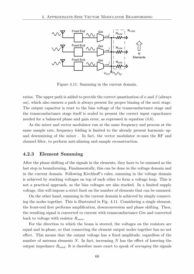
4. Approximate-Sine Vector Modulator Beamforming
RSUMGmFront End
RSUMGmFront End
RSUMGmFront End
i
i
i
N
Elements
RLOAD
VOUT
Figure 4.11: Summing in the current domain.
ratios. The upper path is added to provide the correct quantization of α and β (always
on), which also ensures a path is always present for proper biasing of the next stage.
The output capacitor is reset to the bias voltage of the transconductance stage and
the transconductance stage itself is scaled to present the correct input capacitance
needed for a balanced phase and gain error, as expressed in equation (4.6).
As the mixer and vector modulator run at the same frequency and process at the
same sample rate, frequency folding is limited to the already present harmonic up-
and downmixing of the mixer . In fact, the vector modulator re-uses the RF and
channel filter, to perform anti-aliasing and sample reconstruction.
4.2.3 Element Summing
After the phase shifting of the signals in the elements, they have to be summed as the
last step in beamforming. Fundamentally, this can be done in the voltage domain and
in the current domain. Following Kirchhoff’s rules, summing in the voltage domain
is achieved by stacking voltages on top of each other to form a voltage loop. This is
not a practical approach, as the bias voltages are also stacked. In a limited supply
voltage, this will impose a strict limit on the number of elements that can be summed.
On the other hand, summing in the current domain is achieved by simply connect-
ing the nodes together. This is illustrated in Fig. 4.11. Considering a single element,
the front-end first performs amplification, downconversion and phase shifting. Then,
the resulting signal is converted to current with transconductance Gm and converted
back to voltage with resistor Rsum.
For the direction to which the beam is steered, the voltages on the resistors are
equal and in-phase, so that connecting the element output nodes together has no net
effect. This means that the output voltage has a fixed amplitude, regardless of the
number of antenna elements N . In fact, increasing N has the effect of lowering the
output impedance Rload. It is therefore more exact to speak of averaging the signals
68
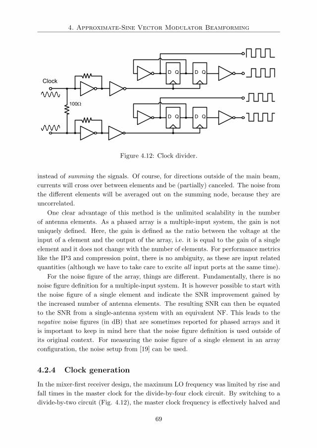
4. Approximate-Sine Vector Modulator Beamforming
D QD Q
100W
D QD Q
Clock
Figure 4.12: Clock divider.
instead of summing the signals. Of course, for directions outside of the main beam,
currents will cross over between elements and be (partially) canceled. The noise from
the different elements will be averaged out on the summing node, because they are
uncorrelated.
One clear advantage of this method is the unlimited scalability in the number
of antenna elements. As a phased array is a multiple-input system, the gain is not
uniquely defined. Here, the gain is defined as the ratio between the voltage at the
input of a element and the output of the array, i.e. it is equal to the gain of a single
element and it does not change with the number of elements. For performance metrics
like the IP3 and compression point, there is no ambiguity, as these are input related
quantities (although we have to take care to excite all input ports at the same time).
For the noise figure of the array, things are different. Fundamentally, there is no
noise figure definition for a multiple-input system. It is however possible to start with
the noise figure of a single element and indicate the SNR improvement gained by
the increased number of antenna elements. The resulting SNR can then be equated
to the SNR from a single-antenna system with an equivalent NF. This leads to the
negative noise figures (in dB) that are sometimes reported for phased arrays and it
is important to keep in mind here that the noise figure definition is used outside of
its original context. For measuring the noise figure of a single element in an array
configuration, the noise setup from [19] can be used.
4.2.4 Clock generation
In the mixer-first receiver design, the maximum LO frequency was limited by rise and
fall times in the master clock for the divide-by-four clock circuit. By switching to a
divide-by-two circuit (Fig. 4.12), the master clock frequency is effectively halved and
69
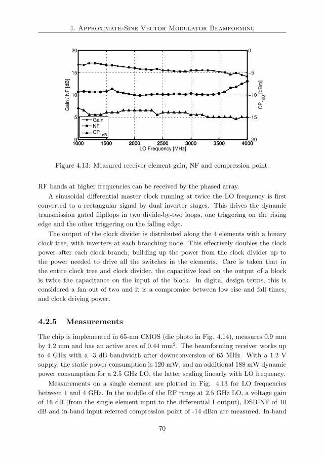
4. Approximate-Sine Vector Modulator Beamforming
1000 1500 2000 2500 3000 3500 40000
5
10
15
20
Gain
/ N
F [dB
]
1000 1500 2000 2500 3000 3500 4000−20
−15
−10
−5
0
LO Frequency [MHz]
CP
1dB [d
Bm
]
Gain
NF
CP1dB
Figure 4.13: Measured receiver element gain, NF and compression point.
RF bands at higher frequencies can be received by the phased array.
A sinusoidal differential master clock running at twice the LO frequency is first
converted to a rectangular signal by dual inverter stages. This drives the dynamic
transmission gated flipflops in two divide-by-two loops, one triggering on the rising
edge and the other triggering on the falling edge.
The output of the clock divider is distributed along the 4 elements with a binary
clock tree, with inverters at each branching node. This effectively doubles the clock
power after each clock branch, building up the power from the clock divider up to
the power needed to drive all the switches in the elements. Care is taken that in
the entire clock tree and clock divider, the capacitive load on the output of a block
is twice the capacitance on the input of the block. In digital design terms, this is
considered a fan-out of two and it is a compromise between low rise and fall times,
and clock driving power.
4.2.5 Measurements
The chip is implemented in 65-nm CMOS (die photo in Fig. 4.14), measures 0.9 mm
by 1.2 mm and has an active area of 0.44 mm2. The beamforming receiver works up
to 4 GHz with a -3 dB bandwidth after downconversion of 65 MHz. With a 1.2 V
supply, the static power consumption is 120 mW, and an additional 188 mW dynamic
power consumption for a 2.5 GHz LO, the latter scaling linearly with LO frequency.
Measurements on a single element are plotted in Fig. 4.13 for LO frequencies
between 1 and 4 GHz. In the middle of the RF range at 2.5 GHz LO, a voltage gain
of 16 dB (from the single element input to the differential I output), DSB NF of 10
dB and in-band input referred compression point of -14 dBm are measured. In-band
70
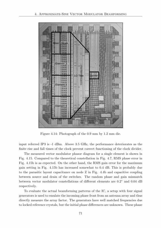
4. Approximate-Sine Vector Modulator Beamforming
Mixer Slices
Element 3
Element 2
Element 4
LO Tree Divider
Figure 4.14: Photograph of the 0.9 mm by 1.2 mm die.
input referred IP3 is -1 dBm. Above 3.5 GHz, the performance deteriorates as the
finite rise and fall times of the clock prevent correct functioning of the clock divider.
The measured vector modulator phasor diagram for a single element is shown in
Fig. 4.15. Compared to the theoretical constellation in Fig. 4.7, RMS phase error in
Fig. 4.15b is as expected. On the other hand, the RMS gain error for the maximum
gain setting in Fig. 4.15b has increased somewhat to 0.4 dB. This is probably due
to the parasitic layout capacitance on node Z in Fig. 4.4b and capacitive coupling
between source and drain of the switches. The random phase and gain mismatch
between vector modulator constellations of different elements are 0.2 and 0.04 dB
respectively.
To evaluate the actual beamforming patterns of the IC, a setup with four signal
generators is used to emulate the incoming phase front from an antenna array and thus
directly measure the array factor. The generators have well matched frequencies due
to locked reference crystals, but the initial phase differences are unknown. These phase
71
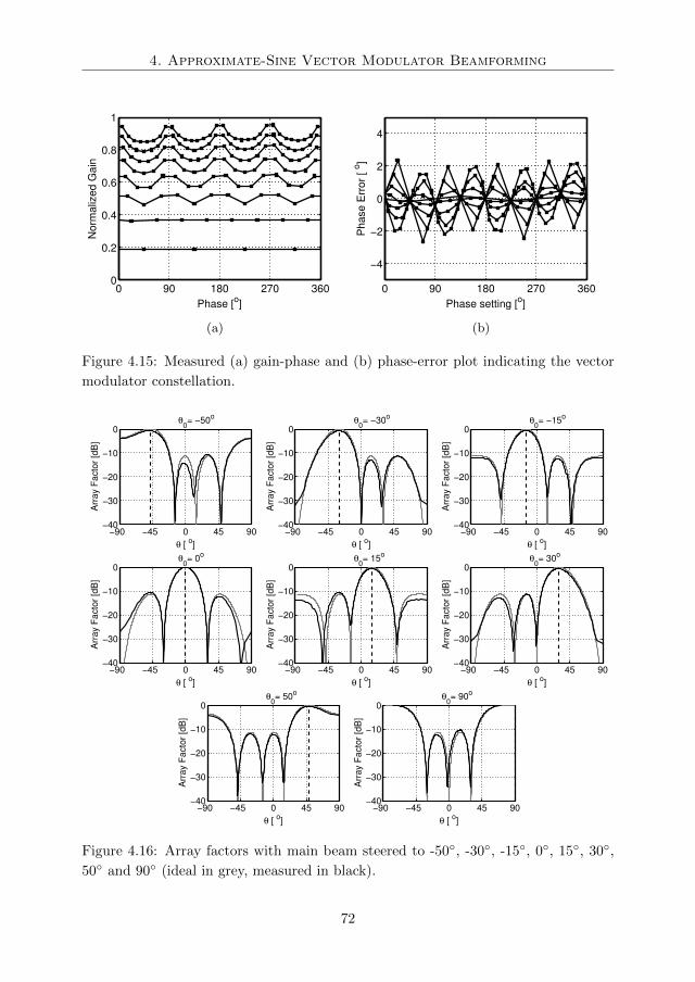
4. Approximate-Sine Vector Modulator Beamforming
0 90 180 270 3600
0.2
0.4
0.6
0.8
1
Phase [o]
No
rmalized G
ain
(a)
0 90 180 270 360
−4
−2
0
2
4
Phase setting [o]
Phase
Err
or
[ o]
(b)
Figure 4.15: Measured (a) gain-phase and (b) phase-error plot indicating the vector
modulator constellation.
−90 −45 0 45 90−40
−30
−20
−10
0
θ [ o]
Arr
ay F
acto
r [d
B]
θ0= −50
o
−90 −45 0 45 90−40
−30
−20
−10
0
θ [ o]
Arr
ay F
acto
r [d
B]
θ0= −30
o
−90 −45 0 45 90−40
−30
−20
−10
0
θ [ o]
Arr
ay F
acto
r [d
B]
θ0= −15
o
−90 −45 0 45 90−40
−30
−20
−10
0
θ [ o]
Arr
ay F
acto
r [d
B]
θ0= 0
o
−90 −45 0 45 90−40
−30
−20
−10
0
θ [ o]
Arr
ay F
acto
r [d
B]
θ0= 15
o
−90 −45 0 45 90−40
−30
−20
−10
0
θ [ o]
Arr
ay F
acto
r [d
B]
θ0= 30
o
−90 −45 0 45 90−40
−30
−20
−10
0
θ [ o]
Arr
ay F
acto
r [d
B]
θ0= 50
o
−90 −45 0 45 90−40
−30
−20
−10
0
θ [ o]
Arr
ay F
acto
r [d
B]
θ0= 90
o
Figure 4.16: Array factors with main beam steered to -50, -30, -15, 0, 15, 30,
50 and 90 (ideal in grey, measured in black).
72
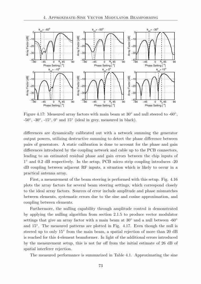
4. Approximate-Sine Vector Modulator Beamforming
−90 −45 0 45 90−40
−30
−20
−10
0
θ0
Phase Setting [ o]
Arr
ay F
acto
r [d
B]
θint
= −60o
−90 −45 0 45 90−40
−30
−20
−10
0
θ0
Phase Setting [ o]
Arr
ay F
acto
r [d
B]
θint
= −50o
−90 −45 0 45 90−40
−30
−20
−10
0
θ0
Phase Setting [ o]
Arr
ay F
acto
r [d
B]
θint
= −30o
−90 −45 0 45 90−40
−30
−20
−10
0
θ0
Phase Setting [ o]
Arr
ay F
acto
r [d
B]
θint
= −15o
−90 −45 0 45 90−40
−30
−20
−10
0
θ0
Phase Setting [ o]
Arr
ay F
acto
r [d
B]
θint
= 0o
−90 −45 0 45 90−40
−30
−20
−10
0
θ0
Phase Setting [ o]
Arr
ay F
acto
r [d
B]
θint
= 15o
Figure 4.17: Measured array factors with main beam at 30 and null steered to -60,
-50, -30, -15, 0 and 15 (ideal in grey, measured in black).
differences are dynamically calibrated out with a network summing the generator
output powers, utilizing destructive summing to detect the phase difference between
pairs of generators. A static calibration is done to account for the phase and gain
differences introduced by the coupling network and cable up to the PCB connectors,
leading to an estimated residual phase and gain errors between the chip inputs of
1 and 0.2 dB respectively. In the setup, PCB micro strip coupling introduces -20
dB coupling between adjacent RF inputs, a situation which is likely to occur in a
practical antenna array.
First, a measurement of the beam steering is performed with this setup. Fig. 4.16
plots the array factors for several beam steering settings, which correspond closely
to the ideal array factors. Sources of error include amplitude and phase mismatches
between elements, systematic errors due to the sine and cosine approximation, and
coupling between elements.
Furthermore, the nulling capability through amplitude control is demonstrated
by applying the nulling algorithm from section 2.1.5 to produce vector modulator
settings that give an array factor with a main beam at 30 and a null between -60
and 15. The measured patterns are plotted in Fig. 4.17. Even though the null is
steered up to only 15 from the main beam, a spatial rejection of more than 20 dB
is reached for this 4-element beamformer. In light of the additional errors introduced
by the measurement setup, this is not far off from the initial estimate of 26 dB of
spatial interferer rejection.
The measured performance is summarized in Table 4.1. Approximating the sine
73
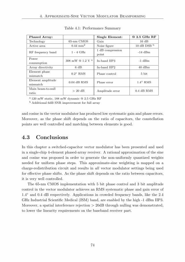
4. Approximate-Sine Vector Modulator Beamforming
Table 4.1: Performance Summary
Phased Array: Single Element: @ 2.5 GHz RF
Technology 65-nm CMOS Gain 16 dB
Active area 0.44 mm2 Noise figure 10 dB DSB b
RF frequency band 1 - 4 GHz1 dB compression
point-14 dBm
Power
consumption308 mW @ 1.2 V a In-band IIP3 -1 dBm
Array directivity 6 dB In-band IIP2 40 dBm
Element phase
mismatch0.2 RMS Phase control 5 bit
Element amplitude
mismatch0.04 dB RMS Phase error 1.4 RMS
Main beam-to-null
ratio> 20 dB Amplitude error 0.4 dB RMS
a 120 mW static, 188 mW dynamic @ 2.5 GHz RFb Additional 6dB SNR improvement for full array
and cosine in the vector modulator has produced low systematic gain and phase errors.
Moreover, as the phase shift depends on the ratio of capacitors, the constellation
points are well controlled and matching between elements is good.
4.3 Conclusions
In this chapter a switched-capacitor vector modulator has been presented and used
in a single-chip 4-element phased-array receiver. A rational approximation of the sine
and cosine was proposed in order to generate the non-uniformly quantized weights
needed for uniform phase steps. This approximate-sine weighting is mapped on a
charge-redistribution circuit and results in all vector modulator settings being used
for effective phase shifts. As the phase shift depends on the ratio between capacitors,
it is very well controlled.
The 65-nm CMOS implementation with 5 bit phase control and 3 bit amplitude
control in the vector modulator achieves an RMS systematic phase and gain error of
1.4 and 0.4 dB respectively. Applications in crowded frequency bands, like the 2.4
GHz Industrial Scientific Medical (ISM) band, are enabled by the high -1 dBm IIP3.
Moreover, a spatial interference rejection > 20dB through nulling was demonstrated,
to lower the linearity requirements on the baseband receiver part.
74
Chapter 5
All-Passive
Switched-Capacitor Phased
Array
In chapter 3, it was demonstrated that a mixer-first architecture can have a large
spurious-free dynamic range. Instrumental for this approach was the use of passive
25% duty cycle mixers. In the frequency domain analysis it was concluded that for
low noise, mixing region switched-RC loops can be used in the mixer design. Even
so, the linearity of the implemented prototype was not limited by the mixer, but by
the active baseband stages.
On the other hand, chapter 4 introduced sampling region switched-RC loops for
the phase shifter design. In this case, a time domain approach proved useful in
finding the circuit transfer function and a very stable phase shifter performance was
demonstrated. In the resulting prototype, it were also the active stages that limited
the linearity performance.
The question arises if the mixer-first architecture can be combined with the sam-
pling region phase shifter, without the use of intervening active stages, as to achieve
a higher linearity. This fits naturally to the strengths of CMOS technology, as such
a design would only use switches and capacitors. Of course, active stages have to be
involved at some point, but can be inserted at places where they hurt the least.
With that in mind, the phased-array system design in Fig. 5.1 is proposed. The
active CMOS baseband circuits are placed after the beamforming summing node, so
that strong interferers can be spatially filtered. These interferers are still present
in the beamforming circuits, which are passive and provide a 50 Ω interface to the
RF ports. RF band filters are necessary to filter out signals at the LO harmonics,
75
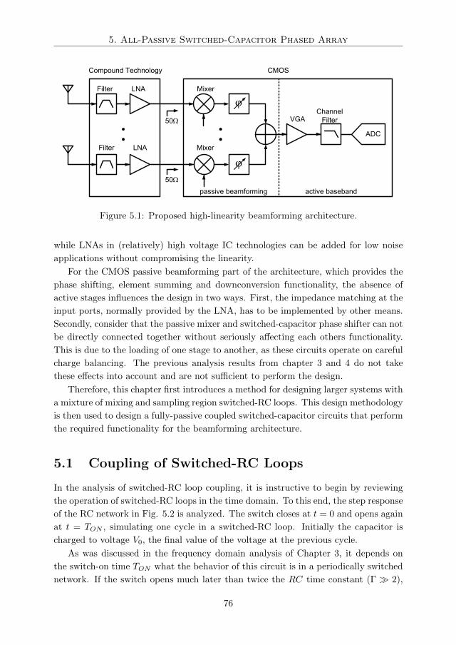
5. All-Passive Switched-Capacitor Phased Array
j
j
ADC
CMOSCompound Technology
passive beamforming active baseband
VGAChannel
Filter
MixerLNAFilter
LNAFilter Mixer
50W
50W
Figure 5.1: Proposed high-linearity beamforming architecture.
while LNAs in (relatively) high voltage IC technologies can be added for low noise
applications without compromising the linearity.
For the CMOS passive beamforming part of the architecture, which provides the
phase shifting, element summing and downconversion functionality, the absence of
active stages influences the design in two ways. First, the impedance matching at the
input ports, normally provided by the LNA, has to be implemented by other means.
Secondly, consider that the passive mixer and switched-capacitor phase shifter can not
be directly connected together without seriously affecting each others functionality.
This is due to the loading of one stage to another, as these circuits operate on careful
charge balancing. The previous analysis results from chapter 3 and 4 do not take
these effects into account and are not sufficient to perform the design.
Therefore, this chapter first introduces a method for designing larger systems with
a mixture of mixing and sampling region switched-RC loops. This design methodology
is then used to design a fully-passive coupled switched-capacitor circuits that perform
the required functionality for the beamforming architecture.
5.1 Coupling of Switched-RC Loops
In the analysis of switched-RC loop coupling, it is instructive to begin by reviewing
the operation of switched-RC loops in the time domain. To this end, the step response
of the RC network in Fig. 5.2 is analyzed. The switch closes at t = 0 and opens again
at t = TON , simulating one cycle in a switched-RC loop. Initially the capacitor is
charged to voltage V0, the final value of the voltage at the previous cycle.
As was discussed in the frequency domain analysis of Chapter 3, it depends on
the switch-on time TON what the behavior of this circuit is in a periodically switched
network. If the switch opens much later than twice the RC time constant (Γ 2),
76
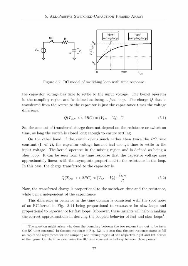
5. All-Passive Switched-Capacitor Phased Array
R
CVIN
t=0
VC
0 2RC0
VIN
V0
TON
VC
(TO
N)
"slow"mixing loop
"fast"sampling loop
Figure 5.2: RC model of switching loop with time response.
the capacitor voltage has time to settle to the input voltage. The kernel operates
in the sampling region and is defined as being a fast loop. The charge Q that is
transferred from the source to the capacitor is just the capacitance times the voltage
difference:
Q(TON >> 2RC) ≈ (VIN − V0) · C. (5.1)
So, the amount of transferred charge does not depend on the resistance or switch-on
time, as long the switch is closed long enough to ensure settling.
On the other hand, if the switch opens much earlier than twice the RC time
constant (Γ 2), the capacitor voltage has not had enough time to settle to the
input voltage. The kernel operates in the mixing region and is defined as being a
slow loop. It can be seen from the time response that the capacitor voltage rises
approximately linear, with the asymptote proportional to the resistance in the loop.
In this case, the charge transferred to the capacitor is:
Q(TON << 2RC) ≈ (VIN − V0) · TONR
(5.2)
Now, the transferred charge is proportional to the switch-on time and the resistance,
while being independent of the capacitance.
This difference in behavior in the time domain is consistent with the spot noise
of an RC kernel in Fig. 3.14 being proportional to resistance for slow loops and
proportional to capacitance for fast loops. Moreover, these insights will help in making
the correct approximations in deriving the coupled behavior of fast and slow loops1.
1The question might arise: why does the boundary between the two regions turn out to be twice
the RC time constant? In the step response in Fig. 5.2, it is seen that the step response starts to fall
on top of the asymptotes for the sampling and mixing region at the respective right and left border
of the figure. On the time axis, twice the RC time constant is halfway between those points.
77
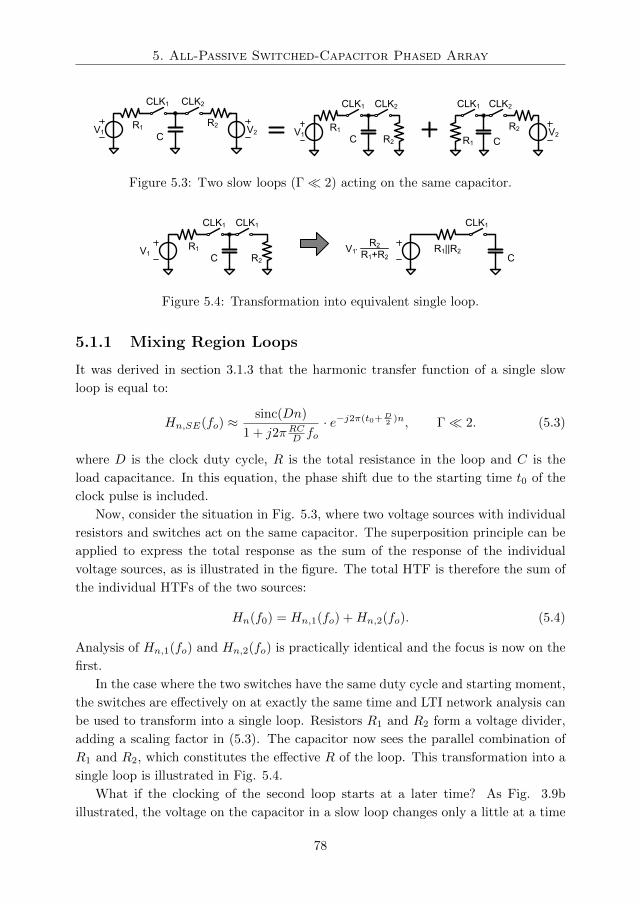
5. All-Passive Switched-Capacitor Phased Array
CLK1
V1R1 V2
R2
C
CLK1
V1R1
C R2
CLK1
V2R2
CR1
CLK2 CLK2 CLK2
Figure 5.3: Two slow loops (Γ 2) acting on the same capacitor.
CLK1
V1R1
C R2
CLK1 CLK1
R1||R2C
R2R1+R2
V1×
Figure 5.4: Transformation into equivalent single loop.
5.1.1 Mixing Region Loops
It was derived in section 3.1.3 that the harmonic transfer function of a single slow
loop is equal to:
Hn,SE(fo) ≈sinc(Dn)
1 + j2πRCD fo· e−j2π(t0+D
2 )n, Γ 2. (5.3)
where D is the clock duty cycle, R is the total resistance in the loop and C is the
load capacitance. In this equation, the phase shift due to the starting time t0 of the
clock pulse is included.
Now, consider the situation in Fig. 5.3, where two voltage sources with individual
resistors and switches act on the same capacitor. The superposition principle can be
applied to express the total response as the sum of the response of the individual
voltage sources, as is illustrated in the figure. The total HTF is therefore the sum of
the individual HTFs of the two sources:
Hn(f0) = Hn,1(fo) +Hn,2(fo). (5.4)
Analysis of Hn,1(fo) and Hn,2(fo) is practically identical and the focus is now on the
first.
In the case where the two switches have the same duty cycle and starting moment,
the switches are effectively on at exactly the same time and LTI network analysis can
be used to transform into a single loop. Resistors R1 and R2 form a voltage divider,
adding a scaling factor in (5.3). The capacitor now sees the parallel combination of
R1 and R2, which constitutes the effective R of the loop. This transformation into a
single loop is illustrated in Fig. 5.4.
What if the clocking of the second loop starts at a later time? As Fig. 3.9b
illustrated, the voltage on the capacitor in a slow loop changes only a little at a time
78
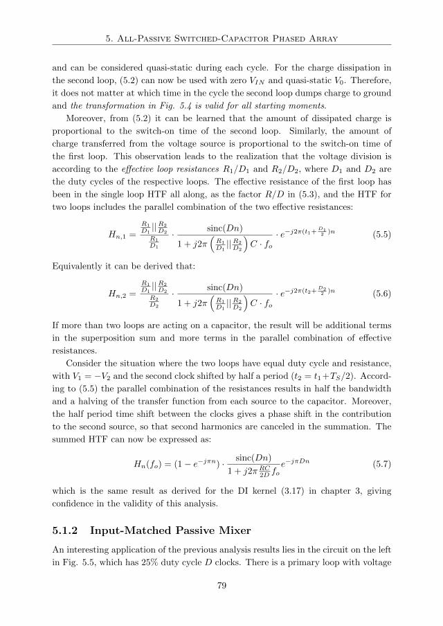
5. All-Passive Switched-Capacitor Phased Array
and can be considered quasi-static during each cycle. For the charge dissipation in
the second loop, (5.2) can now be used with zero VIN and quasi-static V0. Therefore,
it does not matter at which time in the cycle the second loop dumps charge to ground
and the transformation in Fig. 5.4 is valid for all starting moments.
Moreover, from (5.2) it can be learned that the amount of dissipated charge is
proportional to the switch-on time of the second loop. Similarly, the amount of
charge transferred from the voltage source is proportional to the switch-on time of
the first loop. This observation leads to the realization that the voltage division is
according to the effective loop resistances R1/D1 and R2/D2, where D1 and D2 are
the duty cycles of the respective loops. The effective resistance of the first loop has
been in the single loop HTF all along, as the factor R/D in (5.3), and the HTF for
two loops includes the parallel combination of the two effective resistances:
Hn,1 =R1
D1||R2
D2
R1
D1
· sinc(Dn)
1 + j2π(R1
D1||R2
D2
)C · fo
· e−j2π(t1+D12 )n (5.5)
Equivalently it can be derived that:
Hn,2 =R1
D1||R2
D2
R2
D2
· sinc(Dn)
1 + j2π(R1
D1||R2
D2
)C · fo
· e−j2π(t2+D22 )n (5.6)
If more than two loops are acting on a capacitor, the result will be additional terms
in the superposition sum and more terms in the parallel combination of effective
resistances.
Consider the situation where the two loops have equal duty cycle and resistance,
with V1 = −V2 and the second clock shifted by half a period (t2 = t1 +TS/2). Accord-
ing to (5.5) the parallel combination of the resistances results in half the bandwidth
and a halving of the transfer function from each source to the capacitor. Moreover,
the half period time shift between the clocks gives a phase shift in the contribution
to the second source, so that second harmonics are canceled in the summation. The
summed HTF can now be expressed as:
Hn(fo) = (1− e−jπn) · sinc(Dn)
1 + j2πRC2D foe−jπDn (5.7)
which is the same result as derived for the DI kernel (3.17) in chapter 3, giving
confidence in the validity of this analysis.
5.1.2 Input-Matched Passive Mixer
An interesting application of the previous analysis results lies in the circuit on the left
in Fig. 5.5, which has 25% duty cycle D clocks. There is a primary loop with voltage
79
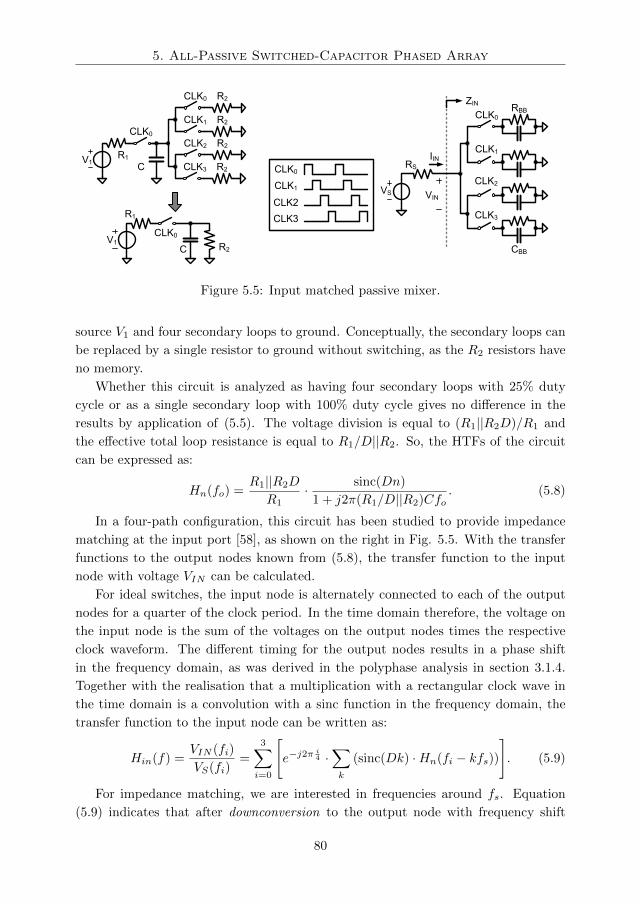
5. All-Passive Switched-Capacitor Phased Array
CLK0
CLK1
CLK2
CLK3
VS
RS
RBB
CBB
ZIN
CLK0
CLK1
CLK2
CLK3
CLK0
V1R1
C
CLK0 R2
CLK1 R2
CLK2 R2
CLK3 R2
CLK0V1
R1
C R2
VIN
IIN
Figure 5.5: Input matched passive mixer.
source V1 and four secondary loops to ground. Conceptually, the secondary loops can
be replaced by a single resistor to ground without switching, as the R2 resistors have
no memory.
Whether this circuit is analyzed as having four secondary loops with 25% duty
cycle or as a single secondary loop with 100% duty cycle gives no difference in the
results by application of (5.5). The voltage division is equal to (R1||R2D)/R1 and
the effective total loop resistance is equal to R1/D||R2. So, the HTFs of the circuit
can be expressed as:
Hn(fo) =R1||R2D
R1· sinc(Dn)
1 + j2π(R1/D||R2)Cfo. (5.8)
In a four-path configuration, this circuit has been studied to provide impedance
matching at the input port [58], as shown on the right in Fig. 5.5. With the transfer
functions to the output nodes known from (5.8), the transfer function to the input
node with voltage VIN can be calculated.
For ideal switches, the input node is alternately connected to each of the output
nodes for a quarter of the clock period. In the time domain therefore, the voltage on
the input node is the sum of the voltages on the output nodes times the respective
clock waveform. The different timing for the output nodes results in a phase shift
in the frequency domain, as was derived in the polyphase analysis in section 3.1.4.
Together with the realisation that a multiplication with a rectangular clock wave in
the time domain is a convolution with a sinc function in the frequency domain, the
transfer function to the input node can be written as:
Hin(f) =VIN (fi)
VS(fi)=
3∑i=0
[e−j2π
i4 ·∑k
(sinc(Dk) ·Hn(fi − kfs))
]. (5.9)
For impedance matching, we are interested in frequencies around fs. Equation
(5.9) indicates that after downconversion to the output node with frequency shift
80
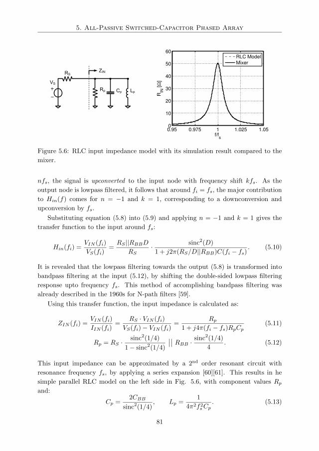
5. All-Passive Switched-Capacitor Phased Array
RS
Rp Cp Lp
VS
ZIN
0.95 0.975 1 1.025 1.050
10
20
30
40
50
60
f/fs
RIN
[Ω
]
RLC Model
Mixer
Figure 5.6: RLC input impedance model with its simulation result compared to the
mixer.
nfs, the signal is upconverted to the input node with frequency shift kfs. As the
output node is lowpass filtered, it follows that around fi = fs, the major contribution
to Hin(f) comes for n = −1 and k = 1, corresponding to a downconversion and
upconversion by fs.
Substituting equation (5.8) into (5.9) and applying n = −1 and k = 1 gives the
transfer function to the input around fs:
Hin(fi) =VIN (fi)
VS(fi)=RS ||RBBD
RS· sinc2(D)
1 + j2π(RS/D||RBB)C(fi − fs). (5.10)
It is revealed that the lowpass filtering towards the output (5.8) is transformed into
bandpass filtering at the input (5.12), by shifting the double-sided lowpass filtering
response upto frequency fs. This method of accomplishing bandpass filtering was
already described in the 1960s for N-path filters [59].
Using this transfer function, the input impedance is calculated as:
ZIN (fi) =VIN (fi)
IIN (fi)=
RS · VIN (fi)
VS(fi)− VIN (fi)=
Rp1 + j4π(fi − fs)RpCp
(5.11)
Rp = RS ·sinc2(1/4)
1− sinc2(1/4)
∣∣∣∣ RBB · sinc2(1/4)
4. (5.12)
This input impedance can be approximated by a 2nd order resonant circuit with
resonance frequency fs, by applying a series expansion [60][61]. This results in he
simple parallel RLC model on the left side in Fig. 5.6, with component values Rpand:
Cp =2CBB
sinc2(1/4), Lp =
1
4π2f2sCp
. (5.13)
81
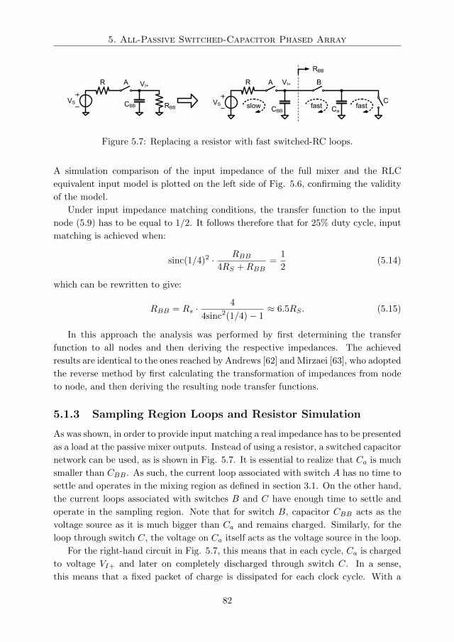
5. All-Passive Switched-Capacitor Phased Array
CBB
A
RBBC
BAVI+
VS
R VI+
CBB CaVS
R
slow fast fast
RBB
Figure 5.7: Replacing a resistor with fast switched-RC loops.
A simulation comparison of the input impedance of the full mixer and the RLC
equivalent input model is plotted on the left side of Fig. 5.6, confirming the validity
of the model.
Under input impedance matching conditions, the transfer function to the input
node (5.9) has to be equal to 1/2. It follows therefore that for 25% duty cycle, input
matching is achieved when:
sinc(1/4)2 · RBB4RS +RBB
=1
2(5.14)
which can be rewritten to give:
RBB = Rs ·4
4sinc2(1/4)− 1≈ 6.5RS . (5.15)
In this approach the analysis was performed by first determining the transfer
function to all nodes and then deriving the respective impedances. The achieved
results are identical to the ones reached by Andrews [62] and Mirzaei [63], who adopted
the reverse method by first calculating the transformation of impedances from node
to node, and then deriving the resulting node transfer functions.
5.1.3 Sampling Region Loops and Resistor Simulation
As was shown, in order to provide input matching a real impedance has to be presented
as a load at the passive mixer outputs. Instead of using a resistor, a switched capacitor
network can be used, as is shown in Fig. 5.7. It is essential to realize that Ca is much
smaller than CBB . As such, the current loop associated with switch A has no time to
settle and operates in the mixing region as defined in section 3.1. On the other hand,
the current loops associated with switches B and C have enough time to settle and
operate in the sampling region. Note that for switch B, capacitor CBB acts as the
voltage source as it is much bigger than Ca and remains charged. Similarly, for the
loop through switch C, the voltage on Ca itself acts as the voltage source in the loop.
For the right-hand circuit in Fig. 5.7, this means that in each cycle, Ca is charged
to voltage VI+ and later on completely discharged through switch C. In a sense,
this means that a fixed packet of charge is dissipated for each clock cycle. With a
82
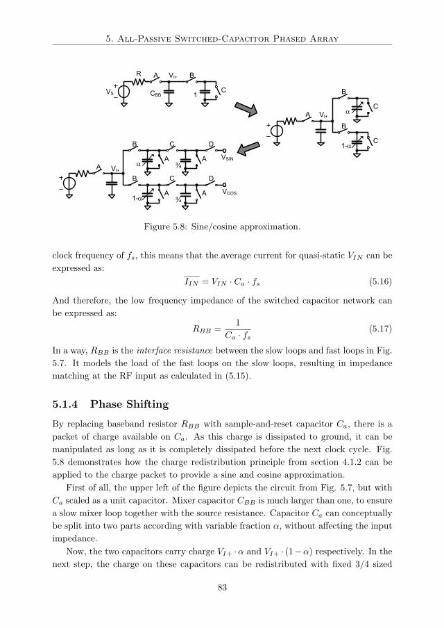
5. All-Passive Switched-Capacitor Phased Array
1-aC
B
VI+Aa
C
B
1-aA
B C
A¾
VI+Aa
A A¾
B C D
D
VSIN
VCOS
C
B
CBB
A
1
VI+
VS
R
Figure 5.8: Sine/cosine approximation.
clock frequency of fs, this means that the average current for quasi-static VIN can be
expressed as:
IIN = VIN · Ca · fs (5.16)
And therefore, the low frequency impedance of the switched capacitor network can
be expressed as:
RBB =1
Ca · fs(5.17)
In a way, RBB is the interface resistance between the slow loops and fast loops in Fig.
5.7. It models the load of the fast loops on the slow loops, resulting in impedance
matching at the RF input as calculated in (5.15).
5.1.4 Phase Shifting
By replacing baseband resistor RBB with sample-and-reset capacitor Ca, there is a
packet of charge available on Ca. As this charge is dissipated to ground, it can be
manipulated as long as it is completely dissipated before the next clock cycle. Fig.
5.8 demonstrates how the charge redistribution principle from section 4.1.2 can be
applied to the charge packet to provide a sine and cosine approximation.
First of all, the upper left of the figure depicts the circuit from Fig. 5.7, but with
Ca scaled as a unit capacitor. Mixer capacitor CBB is much larger than one, to ensure
a slow mixer loop together with the source resistance. Capacitor Ca can conceptually
be split into two parts according with variable fraction α, without affecting the input
impedance.
Now, the two capacitors carry charge VI+ ·α and VI+ · (1−α) respectively. In the
next step, the charge on these capacitors can be redistributed with fixed 3/4 sized
83
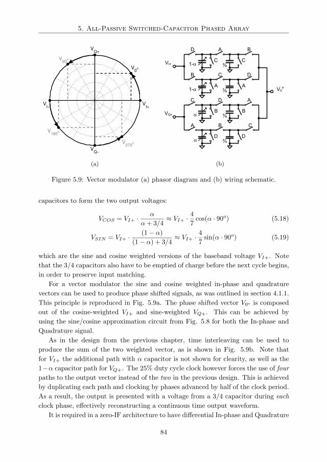
5. All-Passive Switched-Capacitor Phased Array
VI+
VI−
VQ+
VQ−
V0
o
V90
o
V180
o
V270
o
(a)
aB
C D
B
A
¾
1-aA
B C
A
D
¾
aD
A B
D¾
1-aC
D A
C¾
V0o
B
C
VI+
VQ+
(b)
Figure 5.9: Vector modulator (a) phasor diagram and (b) wiring schematic.
capacitors to form the two output voltages:
VCOS = VI+ ·α
α+ 3/4≈ VI+ ·
4
7cos(α · 90o) (5.18)
VSIN = VI+ ·(1− α)
(1− α) + 3/4≈ VI+ ·
4
7sin(α · 90o) (5.19)
which are the sine and cosine weighted versions of the baseband voltage VI+. Note
that the 3/4 capacitors also have to be emptied of charge before the next cycle begins,
in order to preserve input matching.
For a vector modulator the sine and cosine weighted in-phase and quadrature
vectors can be used to produce phase shifted signals, as was outlined in section 4.1.1.
This principle is reproduced in Fig. 5.9a. The phase shifted vector V0o is composed
out of the cosine-weighted VI+ and sine-weighted VQ+. This can be achieved by
using the sine/cosine approximation circuit from Fig. 5.8 for both the In-phase and
Quadrature signal.
As in the design from the previous chapter, time interleaving can be used to
produce the sum of the two weighted vector, as is shown in Fig. 5.9b. Note that
for VI+ the additional path with α capacitor is not shown for clearity, as well as the
1−α capacitor path for VQ+. The 25% duty cycle clock however forces the use of four
paths to the output vector instead of the two in the previous design. This is achieved
by duplicating each path and clocking by phases advanced by half of the clock period.
As a result, the output is presented with a voltage from a 3/4 capacitor during each
clock phase, effectively reconstructing a continuous time output waveform.
It is required in a zero-IF architecture to have differential In-phase and Quadrature
84
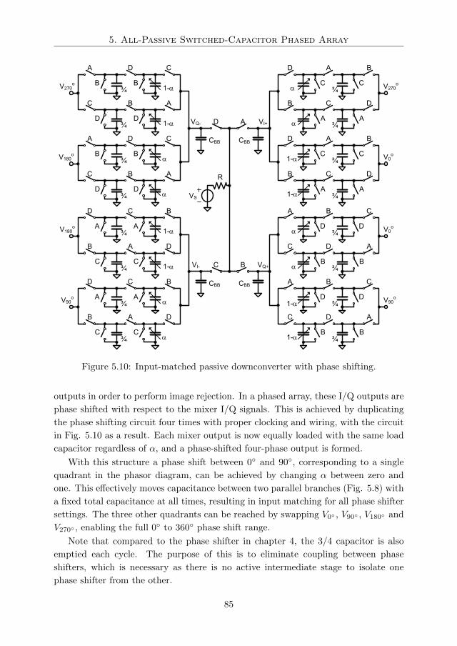
5. All-Passive Switched-Capacitor Phased Array
1-aD
A B
D
C
¾
aB
C D
B
A
¾
1-aB
C D
B¾
aD
A B
D¾
C
A
1-aC
D A
C
B
¾
aA
B C
A
D
¾
1-aA
B C
A¾
aC
D A
C¾
B
D
CBB
VI+
CBB
VQ+
A
B
aA
BC
A
D
¾
1-aC
DA
C
B
¾
aC
DA
C¾
1-aA
BC
A¾
D
B
aB
CD
B
A
¾
1-aD
AB
D
C
¾
aD
AB
D¾
1-aB
CD
B¾
A
C
CBB
VQ-
CBB
VI-
D
C
VS
R
V270o
V0o
V0o
V90o
V270o
V180o
V180o
V90o
Figure 5.10: Input-matched passive downconverter with phase shifting.
outputs in order to perform image rejection. In a phased array, these I/Q outputs are
phase shifted with respect to the mixer I/Q signals. This is achieved by duplicating
the phase shifting circuit four times with proper clocking and wiring, with the circuit
in Fig. 5.10 as a result. Each mixer output is now equally loaded with the same load
capacitor regardless of α, and a phase-shifted four-phase output is formed.
With this structure a phase shift between 0 and 90, corresponding to a single
quadrant in the phasor diagram, can be achieved by changing α between zero and
one. This effectively moves capacitance between two parallel branches (Fig. 5.8) with
a fixed total capacitance at all times, resulting in input matching for all phase shifter
settings. The three other quadrants can be reached by swapping V0 , V90 , V180 and
V270 , enabling the full 0 to 360 phase shift range.
Note that compared to the phase shifter in chapter 4, the 3/4 capacitor is also
emptied each cycle. The purpose of this is to eliminate coupling between phase
shifters, which is necessary as there is no active intermediate stage to isolate one
phase shifter from the other.
85
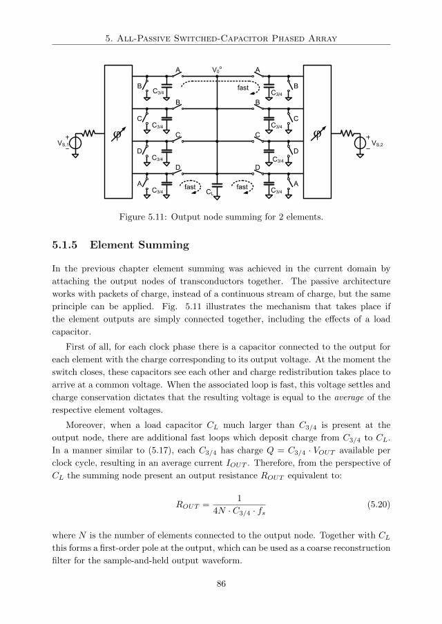
5. All-Passive Switched-Capacitor Phased Array
C
C3/4
B
C3/4
C3/4
A
D
VS,1
C
C3/4
B
C3/4
C3/4
C3/4
A
D
VS,2
CL
j j
fast
fast
fast
C3/4B
C
D
A
B
C
D
A
V0o
Figure 5.11: Output node summing for 2 elements.
5.1.5 Element Summing
In the previous chapter element summing was achieved in the current domain by
attaching the output nodes of transconductors together. The passive architecture
works with packets of charge, instead of a continuous stream of charge, but the same
principle can be applied. Fig. 5.11 illustrates the mechanism that takes place if
the element outputs are simply connected together, including the effects of a load
capacitor.
First of all, for each clock phase there is a capacitor connected to the output for
each element with the charge corresponding to its output voltage. At the moment the
switch closes, these capacitors see each other and charge redistribution takes place to
arrive at a common voltage. When the associated loop is fast, this voltage settles and
charge conservation dictates that the resulting voltage is equal to the average of the
respective element voltages.
Moreover, when a load capacitor CL much larger than C3/4 is present at the
output node, there are additional fast loops which deposit charge from C3/4 to CL.
In a manner similar to (5.17), each C3/4 has charge Q = C3/4 · VOUT available per
clock cycle, resulting in an average current IOUT . Therefore, from the perspective of
CL the summing node present an output resistance ROUT equivalent to:
ROUT =1
4N · C3/4 · fs(5.20)
where N is the number of elements connected to the output node. Together with CLthis forms a first-order pole at the output, which can be used as a coarse reconstruction
filter for the sample-and-held output waveform.
86
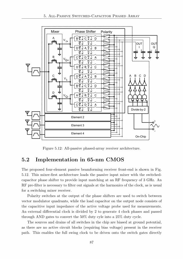
5. All-Passive Switched-Capacitor Phased Array
B DC
D BA
C AD
A CB
D BA
B DC
A CB
C AD
Element 3
Element 2
Element 4
Mixer
OUT
Q
OUT
I
BA C D
PolarityPhase Shifter
On-Chip
Divide-by-2
I+
Q+
I-
Q-
A
B
C
D
V
V
V
V
Figure 5.12: All-passive phased-array receiver architecture.
5.2 Implementation in 65-nm CMOS
The proposed four-element passive beamforming receiver front-end is shown in Fig.
5.12. This mixer-first architecture loads the passive input mixer with the switched-
capacitor phase shifter to provide input matching at an RF frequency of 3 GHz. An
RF pre-filter is necessary to filter out signals at the harmonics of the clock, as is usual
for a switching mixer receiver.
Polarity switches at the output of the phase shifters are used to switch between
vector modulator quadrants, while the load capacitor on the output node consists of
the capacitive input impedance of the active voltage probe used for measurements.
An external differential clock is divided by 2 to generate 4 clock phases and passed
through AND gates to convert the 50% duty cyle into a 25% duty cycle.
The sources and drains of all switches in the chip are biased at ground potential,
as there are no active circuit blocks (requiring bias voltage) present in the receiver
path. This enables the full swing clock to be driven onto the switch gates directly
87
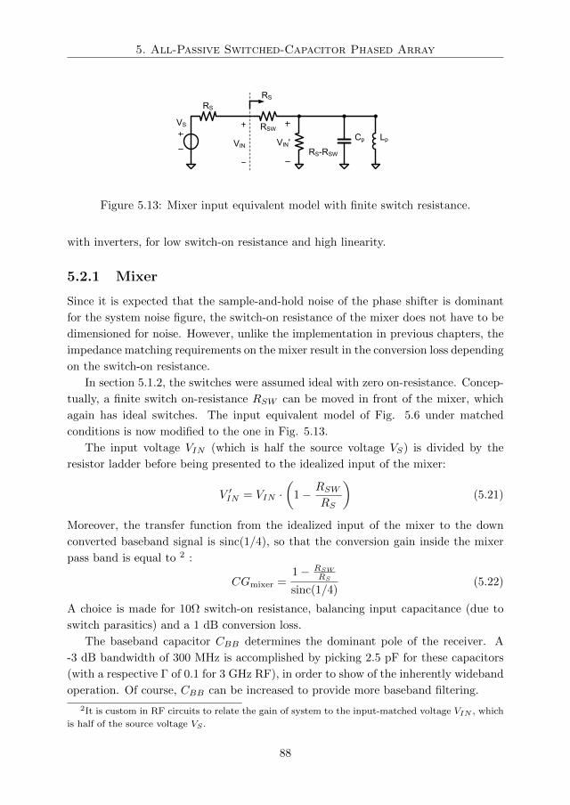
5. All-Passive Switched-Capacitor Phased Array
RS
RS-RSW
Cp Lp
VS
RS
RSW
VIN VIN'
Figure 5.13: Mixer input equivalent model with finite switch resistance.
with inverters, for low switch-on resistance and high linearity.
5.2.1 Mixer
Since it is expected that the sample-and-hold noise of the phase shifter is dominant
for the system noise figure, the switch-on resistance of the mixer does not have to be
dimensioned for noise. However, unlike the implementation in previous chapters, the
impedance matching requirements on the mixer result in the conversion loss depending
on the switch-on resistance.
In section 5.1.2, the switches were assumed ideal with zero on-resistance. Concep-
tually, a finite switch on-resistance RSW can be moved in front of the mixer, which
again has ideal switches. The input equivalent model of Fig. 5.6 under matched
conditions is now modified to the one in Fig. 5.13.
The input voltage VIN (which is half the source voltage VS) is divided by the
resistor ladder before being presented to the idealized input of the mixer:
V ′IN = VIN ·(
1− RSWRS
)(5.21)
Moreover, the transfer function from the idealized input of the mixer to the down
converted baseband signal is sinc(1/4), so that the conversion gain inside the mixer
pass band is equal to 2 :
CGmixer =1− RSW
RS
sinc(1/4)(5.22)
A choice is made for 10Ω switch-on resistance, balancing input capacitance (due to
switch parasitics) and a 1 dB conversion loss.
The baseband capacitor CBB determines the dominant pole of the receiver. A
-3 dB bandwidth of 300 MHz is accomplished by picking 2.5 pF for these capacitors
(with a respective Γ of 0.1 for 3 GHz RF), in order to show of the inherently wideband
operation. Of course, CBB can be increased to provide more baseband filtering.
2It is custom in RF circuits to relate the gain of system to the input-matched voltage VIN , which
is half of the source voltage VS .
88
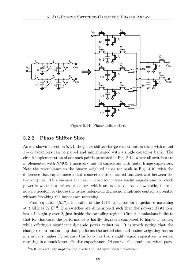
5. All-Passive Switched-Capacitor Phased Array
B
1/16
C
B
1/8
C
B
1/4
C
B
1/2
C
VI+
3/4
D
VSIN
A
A
A
A
A
3/4
D
VCOSA
B
1/16
C
A
1-aA
B C
A¾
aA A
¾
B C D
D
VSIN
VCOS
VI+
Figure 5.14: Phase shifter slice.
5.2.2 Phase Shifter Slice
As was shown in section 5.1.4, the phase shifter charge redistribution slices with α and
1 − α capacitors can be paired and implemented with a single capacitor bank. The
circuit implementation of one such pair is presented in Fig. 5.14, where all switches are
implemented with NMOS transistors and all capacitors with metal fringe capacitors.
Note the resemblance to the binary weighted capacitor bank in Fig. 4.10, with the
difference that capacitance is not connected/disconnected but switched between the
two outputs. This ensures that each capacitor carries useful signals and no clock
power is wasted to switch capacitors which are not used. As a down-side, there is
now no freedom to choose the ratios independently, so no amplitude control is possible
without breaking the impedance matching.
From equation (5.17), the value of the 1/16 capacitor for impedance matching
at 3 GHz is 32 fF 3. The switches are dimensioned such that the slowest (fast) loop
has a Γ slightly over 2, just inside the sampling region. Circuit simulations indicate
that for this case, the performance is hardly degraded compared to higher Γ values,
while offering a significant dynamic power reduction. It is worth noting that the
charge redistribution loop that performs the actual sine and cosine weighting has an
intrinsically higher Γ, because this loop has two roughly equal capacitors in series,
resulting in a much lower effective capacitance. Of course, the dominant switch para-
325 fF was actually implemented due to the 10Ω mixer switch resistance.
89
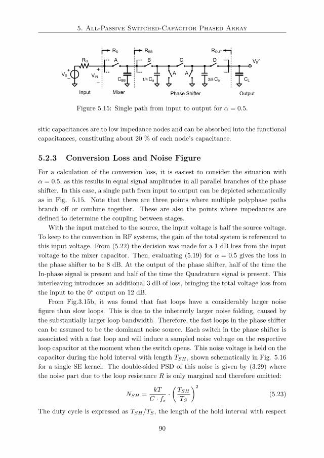
5. All-Passive Switched-Capacitor Phased Array
A
BA
CBB Ca
VS
RS
RBB
C
A
Ca
D
ROUT
CL
V0o
3/81/4
RS
VIN
Mixer Phase Shifter OutputInput
Figure 5.15: Single path from input to output for α = 0.5.
sitic capacitances are to low impedance nodes and can be absorbed into the functional
capacitances, constituting about 20 % of each node’s capacitance.
5.2.3 Conversion Loss and Noise Figure
For a calculation of the conversion loss, it is easiest to consider the situation with
α = 0.5, as this results in equal signal amplitudes in all parallel branches of the phase
shifter. In this case, a single path from input to output can be depicted schematically
as in Fig. 5.15. Note that there are three points where multiple polyphase paths
branch off or combine together. These are also the points where impedances are
defined to determine the coupling between stages.
With the input matched to the source, the input voltage is half the source voltage.
To keep to the convention in RF systems, the gain of the total system is referenced to
this input voltage. From (5.22) the decision was made for a 1 dB loss from the input
voltage to the mixer capacitor. Then, evaluating (5.19) for α = 0.5 gives the loss in
the phase shifter to be 8 dB. At the output of the phase shifter, half of the time the
In-phase signal is present and half of the time the Quadrature signal is present. This
interleaving introduces an additional 3 dB of loss, bringing the total voltage loss from
the input to the 0 output on 12 dB.
From Fig.3.15b, it was found that fast loops have a considerably larger noise
figure than slow loops. This is due to the inherently larger noise folding, caused by
the substantially larger loop bandwidth. Therefore, the fast loops in the phase shifter
can be assumed to be the dominant noise source. Each switch in the phase shifter is
associated with a fast loop and will induce a sampled noise voltage on the respective
loop capacitor at the moment when the switch opens. This noise voltage is held on the
capacitor during the hold interval with length TSH , shown schematically in Fig. 5.16
for a single SE kernel. The double-sided PSD of this noise is given by (3.29) where
the noise part due to the loop resistance R is only marginal and therefore omitted:
NSH =kT
C · fs·(TSHTS
)2
(5.23)
The duty cycle is expressed as TSH/TS , the length of the hold interval with respect
90
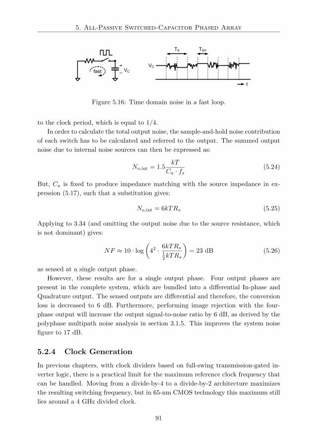
5. All-Passive Switched-Capacitor Phased Array
VCfast
VC
t
TS TSH
Figure 5.16: Time domain noise in a fast loop.
to the clock period, which is equal to 1/4.
In order to calculate the total output noise, the sample-and-hold noise contribution
of each switch has to be calculated and referred to the output. The summed output
noise due to internal noise sources can then be expressed as:
No,int = 1.5kT
Ca · fs(5.24)
But, Ca is fixed to produce impedance matching with the source impedance in ex-
pression (5.17), such that a substitution gives:
No,int = 6kTRs (5.25)
Applying to 3.34 (and omitting the output noise due to the source resistance, which
is not dominant) gives:
NF ≈ 10 · log
(42 · 6kTRs
12kTRs
)= 23 dB (5.26)
as sensed at a single output phase.
However, these results are for a single output phase. Four output phases are
present in the complete system, which are bundled into a differential In-phase and
Quadrature output. The sensed outputs are differential and therefore, the conversion
loss is decreased to 6 dB. Furthermore, performing image rejection with the four-
phase output will increase the output signal-to-noise ratio by 6 dB, as derived by the
polyphase multipath noise analysis in section 3.1.5. This improves the system noise
figure to 17 dB.
5.2.4 Clock Generation
In previous chapters, with clock dividers based on full-swing transmission-gated in-
verter logic, there is a practical limit for the maximum reference clock frequency that
can be handled. Moving from a divide-by-4 to a divide-by-2 architecture maximizes
the resulting switching frequency, but in 65-nm CMOS technology this maximum still
lies around a 4 GHz divided clock.
91
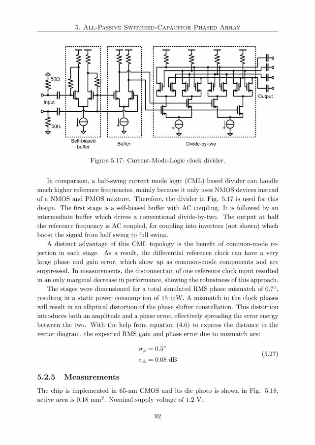
5. All-Passive Switched-Capacitor Phased Array
Input
Output
Divide-by-twoBufferSelf-biased
buffer
50W
50W
Figure 5.17: Current-Mode-Logic clock divider.
In comparison, a half-swing current mode logic (CML) based divider can handle
much higher reference frequencies, mainly because it only uses NMOS devices instead
of a NMOS and PMOS mixture. Therefore, the divider in Fig. 5.17 is used for this
design. The first stage is a self-biased buffer with AC coupling. It is followed by an
intermediate buffer which drives a conventional divide-by-two. The output at half
the reference frequency is AC coupled, for coupling into inverters (not shown) which
boost the signal from half swing to full swing.
A distinct advantage of this CML topology is the benefit of common-mode re-
jection in each stage. As a result, the differential reference clock can have a very
large phase and gain error, which show up as common-mode components and are
suppressed. In measurements, the disconnection of one reference clock input resulted
in an only marginal decrease in performance, showing the robustness of this approach.
The stages were dimensioned for a total simulated RMS phase mismatch of 0.7,
resulting in a static power consumption of 15 mW. A mismatch in the clock phases
will result in an elliptical distortion of the phase shifter constellation. This distortion
introduces both an amplitude and a phase error, effectively spreading the error energy
between the two. With the help from equation (4.6) to express the distance in the
vector diagram, the expected RMS gain and phase error due to mismatch are:
σϕ = 0.5
σA = 0.08 dB(5.27)
5.2.5 Measurements
The chip is implemented in 65-nm CMOS and its die photo is shown in Fig. 5.18,
active area is 0.18 mm2. Nominal supply voltage of 1.2 V.
92
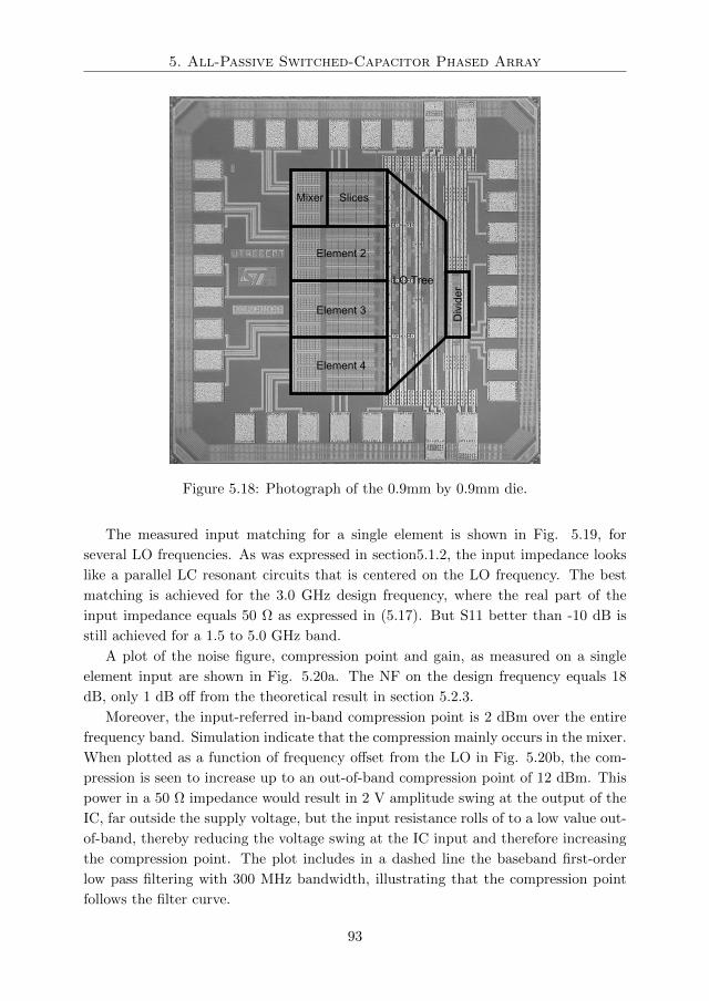
5. All-Passive Switched-Capacitor Phased Array
Mixer Slices
Element 3
Element 2
Element 4
LO Tree
Div
ider
Figure 5.18: Photograph of the 0.9mm by 0.9mm die.
The measured input matching for a single element is shown in Fig. 5.19, for
several LO frequencies. As was expressed in section5.1.2, the input impedance looks
like a parallel LC resonant circuits that is centered on the LO frequency. The best
matching is achieved for the 3.0 GHz design frequency, where the real part of the
input impedance equals 50 Ω as expressed in (5.17). But S11 better than -10 dB is
still achieved for a 1.5 to 5.0 GHz band.
A plot of the noise figure, compression point and gain, as measured on a single
element input are shown in Fig. 5.20a. The NF on the design frequency equals 18
dB, only 1 dB off from the theoretical result in section 5.2.3.
Moreover, the input-referred in-band compression point is 2 dBm over the entire
frequency band. Simulation indicate that the compression mainly occurs in the mixer.
When plotted as a function of frequency offset from the LO in Fig. 5.20b, the com-
pression is seen to increase up to an out-of-band compression point of 12 dBm. This
power in a 50 Ω impedance would result in 2 V amplitude swing at the output of the
IC, far outside the supply voltage, but the input resistance rolls of to a low value out-
of-band, thereby reducing the voltage swing at the IC input and therefore increasing
the compression point. The plot includes in a dashed line the baseband first-order
low pass filtering with 300 MHz bandwidth, illustrating that the compression point
follows the filter curve.
93
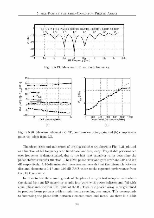
5. All-Passive Switched-Capacitor Phased Array
1 1.5 2 2.5 3 3.5 4 4.5 5 5.5−40
−30
−20
−10
0
RF Frequency [GHz]
S11[d
B]
1.5 GHz
LO
2.0 GHz
LO
2.5 GHz
LO
3.0 GHz
LO
3.5 GHz
LO
4.0 GHz
LO
4.5 GHz
LO
5.0 GHz
LO
Figure 5.19: Measured S11 vs. clock frequency.
2 3 4 5−10
−5
0
5
10
15
20
25
Ga
in, N
F [d
B] /
P1dB [d
Bm
]
LO Frequency [GHz]
NF
P1dB
Gain
(a)
0 200 400 600 800 1000 12000
5
10
15
Offset from LO frequency [MHz]
P1dB [
dB
m]
(b)
Figure 5.20: Measured element (a) NF, compression point, gain and (b) compression
point vs. offset from LO.
The phase steps and gain errors of the phase shifter are shown in Fig. 5.21, plotted
as a function of LO frequency with fixed baseband frequency. Very stable performance
over frequency is demonstrated, due to the fact that capacitor ratios determine the
phase shifter’s transfer function. The RMS phase error and gain error are 2.0 and 0.2
dB respectively. A 10-die mismatch measurement reveals that the mismatch between
dies and elements is 0.4 and 0.06 dB RMS, close to the expected performance from
the clock generator.
In order to test the summing node of the phased array, a test setup is made where
the signal from an RF generator is split four-ways with power splitters and fed with
equal phase into the four RF inputs of the IC. Then, the phased array is programmed
to produce beam patterns with a main beam sweeping over angle. This corresponds
to increasing the phase shift between elements more and more. As there is a 5-bit
94
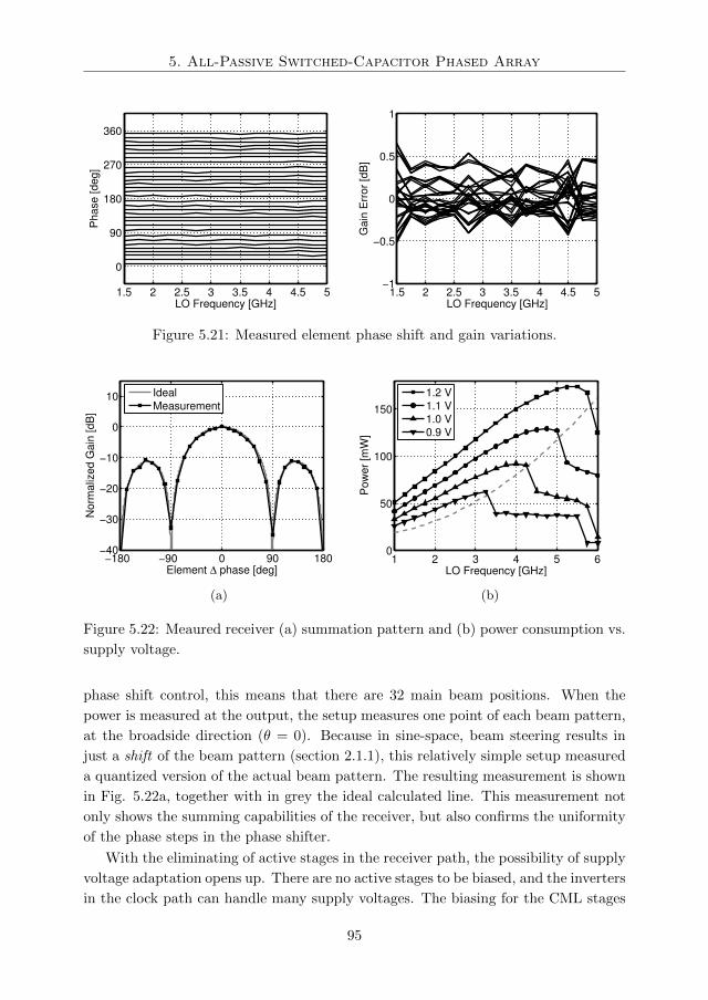
5. All-Passive Switched-Capacitor Phased Array
1.5 2 2.5 3 3.5 4 4.5 5
0
90
180
270
360
LO Frequency [GHz]
Ph
ase [d
eg]
1.5 2 2.5 3 3.5 4 4.5 5−1
−0.5
0
0.5
1
LO Frequency [GHz]
Gain
Err
or
[dB
]
Figure 5.21: Measured element phase shift and gain variations.
−180 −90 0 90 180−40
−30
−20
−10
0
10
Element ∆ phase [deg]
Norm
aliz
ed
Gain
[d
B]
Ideal
Measurement
(a)
1 2 3 4 5 60
50
100
150
LO Frequency [GHz]
Pow
er
[mW
]
1.2 V
1.1 V
1.0 V
0.9 V
(b)
Figure 5.22: Meaured receiver (a) summation pattern and (b) power consumption vs.
supply voltage.
phase shift control, this means that there are 32 main beam positions. When the
power is measured at the output, the setup measures one point of each beam pattern,
at the broadside direction (θ = 0). Because in sine-space, beam steering results in
just a shift of the beam pattern (section 2.1.1), this relatively simple setup measured
a quantized version of the actual beam pattern. The resulting measurement is shown
in Fig. 5.22a, together with in grey the ideal calculated line. This measurement not
only shows the summing capabilities of the receiver, but also confirms the uniformity
of the phase steps in the phase shifter.
With the eliminating of active stages in the receiver path, the possibility of supply
voltage adaptation opens up. There are no active stages to be biased, and the inverters
in the clock path can handle many supply voltages. The biasing for the CML stages
95
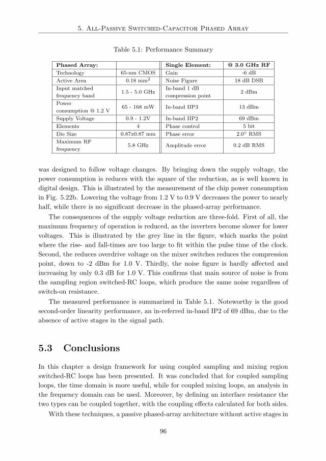
5. All-Passive Switched-Capacitor Phased Array
Table 5.1: Performance Summary
Phased Array: Single Element: @ 3.0 GHz RF
Technology 65-nm CMOS Gain -6 dB
Active Area 0.18 mm2 Noise Figure 18 dB DSB
Input matched
frequency band1.5 - 5.0 GHz
In-band 1 dB
compression point2 dBm
Power
consumption @ 1.2 V65 - 168 mW In-band IIP3 13 dBm
Supply Voltage 0.9 - 1.2V In-band IIP2 69 dBm
Elements 4 Phase control 5 bit
Die Size 0.87x0.87 mm Phase error 2.0 RMS
Maximum RF
frequency5.8 GHz Amplitude error 0.2 dB RMS
was designed to follow voltage changes. By bringing down the supply voltage, the
power consumption is reduces with the square of the reduction, as is well known in
digital design. This is illustrated by the measurement of the chip power consumption
in Fig. 5.22b. Lowering the voltage from 1.2 V to 0.9 V decreases the power to nearly
half, while there is no significant decrease in the phased-array performance.
The consequences of the supply voltage reduction are three-fold. First of all, the
maximum frequency of operation is reduced, as the inverters become slower for lower
voltages. This is illustrated by the grey line in the figure, which marks the point
where the rise- and fall-times are too large to fit within the pulse time of the clock.
Second, the reduces overdrive voltage on the mixer switches reduces the compression
point, down to -2 dBm for 1.0 V. Thirdly, the noise figure is hardly affected and
increasing by only 0.3 dB for 1.0 V. This confirms that main source of noise is from
the sampling region switched-RC loops, which produce the same noise regardless of
switch-on resistance.
The measured performance is summarized in Table 5.1. Noteworthy is the good
second-order linearity performance, an in-referred in-band IP2 of 69 dBm, due to the
absence of active stages in the signal path.
5.3 Conclusions
In this chapter a design framework for using coupled sampling and mixing region
switched-RC loops has been presented. It was concluded that for coupled sampling
loops, the time domain is more useful, while for coupled mixing loops, an analysis in
the frequency domain can be used. Moreover, by defining an interface resistance the
two types can be coupled together, with the coupling effects calculated for both sides.
With these techniques, a passive phased-array architecture without active stages in
96

5. All-Passive Switched-Capacitor Phased Array
the signal path has been proposed, which merges the passive mixer and approximate-
sine phase shifter work together in one design. The coupling between mixer and
phase shifter works two-fold, performing impedance matching at the mixer side and
providing charge for the phase shifter’s charge redistribution process.
The 65-nm CMOS 4-element receiver implementation demonstrates the phased-
array capabilities and the high linearity inherent to this passive design. It was found
that the filtering at the input node of the IC results in a very high 12 dBm out-of-band
compression point, fitting well to the requirements for interferer rejection.
97
Chapter 6
Conclusions
6.1 Summary and Conclusions
In chapter 1, an introduction to single-antenna and multi-antenna wireless systems
was given. The beamforming capabilities of a phased array system and the capacity-
increasing capabilities of spatial multiplexing systems were highlighted, along with
the intrinsic differences between them. Furthermore, the trends in advanced CMOS
have been sketched, along with the difference in device compatibility compared to
compound technologies.
In chapter 2, the fundamental properties of linear phased arrays were summa-
rized first. The basic beam pattern was introduced and the effects on it by beam-
steering, amplitude tapering and the phase shifter approximation was summarized,
along with the degradation due to errors in the array. Next, a framework for in-
cluding downconversion in the beamforming architecture has been presented, along
with transformation methods to move time delay and/or phase shift between the RF,
LO and IF domain. It was found that the reallocation of the beamforming to the
LO or RF domain can give rise to beam squinting, as is the case with the phase
shifter approximation in general array theory. Furthermore, the linearity and sen-
sitivity properties of beamforming circuit implementations were covered, concluding
that beamforming can be viewed as a form of impedance scaling.
In chapter 3, the use of switched-RC donwconverters in a mixer-first receiver
architecture was analyzed. It was shown that a broad range of switched-RC samplers
and mixers can be understood to be an assembly of simple kernels with polyphase
clock timing. A unified frequency domain description was derived, highlighting the
similar- ity in operation of these circuits. Moreover, it was shown that there are
two distinct operating regions of the kernels, depending on the loop bandwidth with
respect to the clock frequency and duty cycle. Analysis shows that using a 25%
98
6. Conclusions
duty cycle switched-RC kernel with low loop bandwidth and a 4-phase clock provides
a low fundamental conversion loss and noise figure, while being compatible with a
I/Q image-reject architecture. This configura- tion, together with baseband feedback
amplifiers, is implemented in a 65nm CMOS implementation and achieves 79 dB of
SFDR in 1 MHz bandwidth, which is in the range of commercial spectrum analyzers.
In chapter 4, a switched-capacitor vector modulator was presented and used in
a single-chip 4-element phased-array receiver. A rational approximation of the sine
and cosine was proposed in order to generate the non-uniformly quantized weights
needed for uniform phase steps. This approximate-sine weighting is mapped on a
charge-redistribution circuit and results in all vector modulator settings being used
for effective phase shifts. As the phase shift depends on the ratio between capacitors, it
is very well controlled. The 65-nm CMOS implementation with 5 bit phase control and
3 bit amplitude control in the vector modulator achieves an RMS systematic phase
and gain error of 1.4 and 0.4 dB respectively. Applications in crowded frequency
bands, like the 2.4 GHz ISM band, are enabled by the high -1 dBm IIP3. Moreover,
a spatial interference rejection > 20dB through nulling was demonstrated, to lower
the linearity requirements on the baseband receiver part.
In chapter 5, a design framework for using coupled sampling and mixing region
switched-RC loops has been presented. It was concluded that for coupled sampling
loops, the time domain is more useful, while for coupled mixing loops, an analysis in
the frequency domain can be used. Moreover, by defining an interface resistance the
two types can be coupled together, with the coupling effects calculated for both sides.
With these techniques, a passive phased-array architecture without active stages in
the signal path has been proposed, which merges the passive mixer and approximate-
sine phase shifter work together in one design. The coupling between mixer and
phase shifter works two-fold, performing impedance matching at the mixer side and
providing charge for the phase shifter’s charge redistribution process. The 65-nm
CMOS 4-element receiver implementation demonstrates the phased-array capabilities
and the high linearity inherent to this passive design. It was found that the filtering
at the input node of the IC results in a very high 12 dBm out-of-band compression
point, fitting well to the requirements for interferer rejection.
6.2 Original Contributions
• The rigorous mathematical derivation of the transfer function for a switched-RC
kernel, unifying the description of mixer and sampler circuits. (chapter 3)
• The concept and design of passive mixer-first receiver architectures. (chapters
3 and 5 )
99
6. Conclusions
• A rational approximation for the sine and cosine needed in a vector modula-
tor phase shifter, which is equal to the transfer function of a simple charge
redistribution switched capacitor circuit. (chapter 4)
• The design of a switched-RC vector modulator, operating at the same frequency
as the passive mixer, thereby avoiding extra folding of the frequency spectrum.
(chapter 4)
• A design method for coupling mixing and sampling region switched-RC kernels
through the definition of the interface resistance. (chapter 5)
• The design of a fully passive beamforming receiver, achieving simultaneous input
matching, downconversion, phase shifting and element summing. (chapter 5)
6.3 Future Work
The increasing integration level in CMOS, so essential for its economic success, has a
profound effect on the development of circuits for wireless communications. Not only
does the smaller feature size enable faster switching speeds, but also the partitioning of
a receiver in lots of multiple slices, for example in the multi-path polyphase technique
(chapter 3). As a result, looking at a receiver frontend as a whole is preferred over
the classical partitioning in separate LNA, mixer, baseband filter, etc.
This is illustrated by the significant research attention for passive mixer-first re-
ceiver architectures (chapter 3) in the past few years, for applications in low-power
wireless sensor nodes [47] and software defined radio [58] [64]. The inherently high
linearity and flexibility in RF frequency of these architectures lends itself well for these
applications, albeit at the cost of a somewhat higher noise figure than tuned receivers.
Recently, a passive mixer-first receiver with noise canceling has been presented [65],
bringing down the noise figure to 2 dB.
In the design of the fully passive beamforming receiver (chapter 5) it was derived
that the passive mixer transforms the baseband lowpass filter to an RF bandpass
filter. This principle was already known in the 1960s [59], but its switched-RC im-
plementation shows great promise for providing high-Q integrated filters in CMOS.
Implementations of 2nd order [66] [67] and 4th order [68] bandpass butterworth filters
with Q values as high as 57 have been published.
There has been some further research on receiver beamforming in the lower fre-
quency bands. A 4 GHz beamformer in 90-nm CMOS [69] performs the phase shifting
in the LO domain (chapter 2) by interpolating between the phases of a multi-phase
clock, exploiting the good timing accuracy of clocks in CMOS. In 0.13-µm CMOS,
a 5-6 GHz 8-element Butler matrix has been presented [70], which is able to form 8
beams simultaneously.
100
6. Conclusions
Looking at the work presented in this thesis, there are several directions for future
innovations. The presented beamforming receivers (chapters 4 and 5) are based on
vector modulation with sampling region switched-RC networks. In the mathematical
analysis of switched-RC kernels (chapter 3) it was derived that the mixing region has
a significantly lower noise contribution compared to the sampling region. Therefore,
a design utilizing only mixing region kernels is expected to have a much lower noise
figure. One obstacle in the implementation of such a design is the amplitude weighting
in the vector modulator. Changing the capacitance in coupled mixing region RC loops
only results in changing the bandwidth. For amplitude weighting, it is necessary to
change the effective resistance, i.e. duty cycle times resistance, of the loop. One
prospect would be to change the duty cycle with accurate timing in the clocks.
Power consumption is always important for mobile devices. The presented designs
offer state-of-the-art performance, but at the cost of significantly higher power con-
sumption than classical RF frontends. It is expected that wideband / widely-tunable
frontends dissipate more power than tuned frontends, but some power savings are al-
ways welcome. A large portion of the power consumption of the switched-RC designs
in this thesis is coming from driving the MOSFET switches. By applying resonant
clocking, some of the energy can be reused from clock cycle to clock cycle. This limits
the clock waveform to a sinusoid, the effect of which on circuit performance has to
be evaluated. Of course, power savings can also be reached by switching to circuit
topologies which require fewer switches. Also in this respect, an all-mixing-region
switched-RC beamforming design looks promising.
Another open end is how amplitude control can be build into the fully passive
beamforming receiver (chapter 5). This design depends on the precise dissipation
of signal energy in the vector modulator to achieve impedance matching. For lower
amplitude settings, the vector modulator does not dissipate enough energy, effectively
raising the input impedance. One solution is to enable extra dissipation switches for
lower amplitudes settings.
Finally, it must be mentioned that no mathematical analysis of distortion in the
switched-RC circuits in this thesis is given. The circuit simulations indicate that with
a clock swing of the full supply voltage on the gate of the MOSFET switches, high
linearity figures are reliable achieved. In fact, the two mixed active/passive designs
(chapters 3 and 4) show that the linearity is limited by the active circuits. But still, it
would be insightful to analyze what is causing the linearity limitations in the passive
circuits and how these limitations can eventually be mitigated.
101
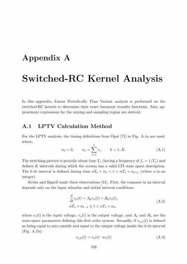
Appendix A
Switched-RC Kernel Analysis
In this appendix, Linear Periodically Time Variant analysis is performed on the
switched-RC kernels to determine their exact harmonic transfer functions. Also, ap-
proximate expressions for the mixing and sampling region are derived.
A.1 LPTV Calculation Method
For the LPTV analysis, the timing definitions from Opal [71] in Fig. A.1a are used,
where:
σ0 = 0, σk =
k∑i=1
τi, k = 1..K. (A.1)
The switching pattern is periodic about time Ts (having a frequency of fs = 1/Ts) and
defines K intervals during which the system has a valid LTI state space description.
The k-th interval is defined during time nTs + σk < t < nTs + σk+1 (where n is an
integer).
Strom and Signell made three observations [51]. First, the response in an interval
depends only on the input stimulus and initial interval conditions:
d
dtvo(t) = Akvo(t) +Bkvi(t),
nTs + σk−1 ≤ t < nTs + σk,
(A.2)
where vi(t) is the input voltage, vo(t) is the output voltage, and Ak and Bk are the
state-space parameters defining this first order system. Secondly, if vo,k(t) is defined
as being equal to zero outside and equal to the output voltage inside the k-th interval
(Fig. A.1b):
vo,k(t) = vo(t) · wk(t) (A.3)
102
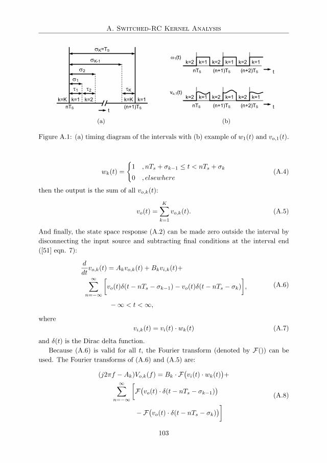
A. Switched-RC Kernel Analysis
t
k=1 k=2 k=K k=1k=K
t1 t2 tK
s1
s2
sK-1
sK=TS
nTS (n+1)TS
(a)
t
k=1 k=2
nTS (n+1)TS
k=1 k=2 k=1k=2
(n+2)TS
vo,1(t)
t
k=1 k=2
nTS (n+1)TS
k=1 k=2 k=1k=2
(n+2)TS
w1(t)
(b)
Figure A.1: (a) timing diagram of the intervals with (b) example of w1(t) and vo,1(t).
wk(t) =
1 , nTs + σk−1 ≤ t < nTs + σk
0 , elsewhere(A.4)
then the output is the sum of all vo,k(t):
vo(t) =
K∑k=1
vo,k(t). (A.5)
And finally, the state space response (A.2) can be made zero outside the interval by
disconnecting the input source and subtracting final conditions at the interval end
([51] eqn. 7):
d
dtvo,k(t) = Akvo,k(t) +Bkvi,k(t)+
∞∑n=−∞
[vo(t)δ(t− nTs − σk−1)− vo(t)δ(t− nTs − σk)
],
−∞ < t <∞,
(A.6)
where
vi,k(t) = vi(t) · wk(t) (A.7)
and δ(t) is the Dirac delta function.
Because (A.6) is valid for all t, the Fourier transform (denoted by F()) can be
used. The Fourier transforms of (A.6) and (A.5) are:
(j2πf −Ak)Vo,k(f) = Bk · F(vi(t) · wk(t)
)+
∞∑n=−∞
[F(vo(t) · δ(t− nTs − σk−1)
)−F
(vo(t) · δ(t− nTs − σk)
)] (A.8)
103
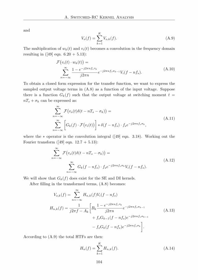
A. Switched-RC Kernel Analysis
and
Vo(f) =
K∑k=1
Vo,k(f). (A.9)
The multiplication of wk(t) and vi(t) becomes a convolution in the frequency domain
resulting in ([49] eqn. 6.20 + 5.13):
F(vi(t) · wk(t)
)=
∞∑n=−∞
1− e−j2πnfsτkj2πn
e−j2πnfsσk−1Vi(f − nfs).(A.10)
To obtain a closed form expression for the transfer function, we want to express the
sampled output voltage terms in (A.8) as a function of the input voltage. Suppose
there is a function Gk(f) such that the output voltage at switching moment t =
nTs + σk can be expressed as:
∞∑n=−∞
F(vo(t)δ(t− nTs − σk)
)=
∞∑n=−∞
[Gk(f) · F
(vi(t)
)]∗ δ(f − nfs) · fse−j2πnfsσk ,
(A.11)
where the ∗ operator is the convolution integral ([49] eqn. 3.18). Working out the
Fourier transform ([49] eqn. 12.7 + 5.13):
∞∑n=−∞
F(vo(t)δ(t− nTs − σk)
)=
∞∑n=−∞
Gk(f − nfs) · fse−j2πnfsσkVi(f − nfs).(A.12)
We will show that Gk(f) does exist for the SE and DI kernels.
After filling in the transformed terms, (A.8) becomes:
Vo,k(f) =
∞∑n=−∞
Hn,k(f)Vi(f − nfs)
Hn,k(f) =1
j2πf −Ak
[Bk
1− e−j2πnfsτkj2πn
e−j2πnfsσk−1
+ fsGk−1(f − nfs)e−j2πnfsσk−1
− fsGk(f − nfs)e−j2πnfsσk].
(A.13)
According to (A.9) the total HTFs are then:
Hn(f) =
K∑k=1
Hn,k(f). (A.14)
104
A. Switched-RC Kernel Analysis
S0
S1
TS
DTS½TS
Vi
R=RS+RONS0
CVo
Figure A.2: Single-ended (SE) kernel.
The substitution of (A.13) into (A.14) is in the form of the HTFs definition (3.2)
if the following notation is introduced:
fo = f fi = f − nfs. (A.15)
We see that Gk must have the input frequency fi as argument.
A.2 SE and DI Kernel Calculation
The SE kernel (Fig. A.2) has two intervals. Linear analysis reveals that the switch-on
interval (k = 1) has the state space description:
d
dtvo(t) = − 1
RCvo(t) +
1
RCvi(t), nTs ≤ t < nTs + σ1 (A.16)
so A1 = − 1RC ≡ −2πfrc and B1 = 1
RC ≡ 2πfrc. The switch-of interval (k = 2) has
the state space description:
d
dtvo(t) = 0, nTs + σ1 ≤ t < (n+ 1)Ts (A.17)
so A2 = 0 and B2 = 0.
The switching-moment transfer functions Gk(fi) are determined for the SE kernel
in Fig. 3.7b. During an interval the LTI system response includes a zero-input term
and a zero-initial-value term ([49] eqn. 8.29 + eqn. 8.41):
vo,k(t) =φk(t− t0)vo,k(t0)
+Bk
∫ t
t0
φk(t− τ)vi(τ)dτ
φk(t) =eAkt
(A.18)
For sinusoidal input (vi(t) = ej2πft) the solution can be calculated directly. During
interval 1:
vo,1(t) =e−2πfrc(t−t0)vo,1(t0)
+1
1 + j ffrc
[ej2πf(t−t0) − e−2πfrc(t−t0)
]ej2πft0
(A.19)
105
A. Switched-RC Kernel Analysis
and interval 2:
vo,2(t) = vo,2(t0). (A.20)
Filling in t0 = nTs and t = nTs + σ1 into (A.19) gives the output voltage at the
interval end vo,1(nTs + σ1) given the input and the initial value vo,1(nTs). Since the
output voltage is continuous, the initial value of an interval is equal to the final value
of the previous interval:
vo,2(nTs + σ1) = limt′↑σ1
vo,1(nTs + t′)
vo,1((n+ 1)Ts) = limt′↑σ2
vo,2(nTs + t′).(A.21)
Furthermore, (A.20) gives:
vo,2(nTs + σ1) = limt′↑σ2
vo,2(nTs + t′). (A.22)
By chaining these expressions, the output voltage after a full cycle can be expressed
as:
vo((n+ 1)Ts) =e−2πfrcτ1vo(nTs)
+1
1 + j ffrc
[ej2πfτ1 − e−2πfrcτ1
]ej2πfnTs .
(A.23)
This result can be viewed as a difference equation with a solution that consists
of a steady state and a transient response. For a frequency domain description the
transient response can be discarded. With the Z-transform it can be calculated that
a difference equation of the form:
vo((n+ 1)Ts) = α · vo(nTs) + β · ej2πfnTs (A.24)
has the steady state solution ([49] eqn. 13.32):
vo(nTs) =β
ej2πfTs − α· ej2πfnTs (A.25)
Applying (A.25) to (A.23) gives:
vo(nTs) =
[ej2πfτ1 − e−2πfrcτ1
ej2πfTs − e−2πfrcτ1
1
1 + j ffrc
]ej2πfnTs , (A.26)
where the term between brackets is defined as G0(f). We will now show that this is
indeed the G0 as defined in (A.11).
Equation (A.26) is still in the discrete time domain and gives the output voltage
sampled at the switching moments. By inserting delta impulse functions, (A.26) is
brought into the continuous time domain:
∞∑n=−∞
vo(t)δ(t− nTs) =
∞∑n=−∞
G0(f) · ej2πftδ(t− nTs). (A.27)
106
A. Switched-RC Kernel Analysis
The above equation gives the output at the switching moments for a single input
sinusoid, represented by ej2πft. After replacing ej2πft by the more generic notation
vi(t), we can take the Fourier transform of (A.27), resulting in:
∞∑n=−∞
F(vo(t)δ(t− nTs)
)=
∞∑n=−∞
[G0(f) · F
(vi(t)
)]∗ δ(f − nfs) · fs.
(A.28)
This was derived for vi(t) being a single sinusoidal input, but because the system is
linear, it actually holds for any input signal vi(t).
Equation (A.28) corresponds to the definition of G0 in (A.11). The same can be
done for vo(nTs + σ1) and vo(nTs + σ2) to find:
G1(f) = G0(f)ej2πfτ2
G2(f) = G0(f).(A.29)
For the two intervals, (A.13) is evaluated by inserting Ak, Bk and Gk:
Hn,1(f) =frc
jf + frc
1− e−j2πnfsτ1j2πn
− jf
jf + frcfsej2πfτ2 − 1
j2πfG0(f − nfs)
Hn,2(f) =fsej2πfτ2 − 1
j2πfG0(f − nfs).
(A.30)
Summing according to (A.14) and applying
1− jf
jf + frc=
frcjf + frc
(A.31)
gives the HTFs, which are a function of the output frequency fo = f . According to
(A.15):
Hn(fo) =
frcjfo + frc
[1− e−j2πnfsτ1
j2πn+ fs
ej2πfoτ2 − 1
j2πfoG0(fo − nfs)
].
(A.32)
This expression can be simplified. The duty cycle D is the duration of the first
interval relative to the period time:
D =τ1Ts
= τ1fs, (1−D) =τ2Ts
= τ2fs. (A.33)
So that the SE kernel transfer function becomes:
Hn(fo) =1
1 + j fofrc
·[
1− e−j2πDn
j2πn+ej2π(1−D)fo/fs − 1
j2πfo/fsG0(fo − nfs)
](A.34)
107

A. Switched-RC Kernel Analysis
S0
S1
TS
DTS½TS
½ViR
S0C
Vo
½Vi S1
Figure A.3: Differential (DI) kernel.
For the DI kernel in Fig. A.3, the same procedure is used. The DI kernel has four
intervals. The first interval (nTs ≤ t < (n+D)Ts) has duty cycle D , with:
d
dtvo(t) = − 1
RCvo(t) +
1
2RCvi(t). (A.35)
The second interval ((n+D)Ts ≤ t < (n+ 12 )Ts) ends after half the period time :
d
dtvo(t) = 0. (A.36)
In the third interval ((n+ 12 )Ts ≤ t < (n+ 1
2 +D)Ts) the negative input is connected:
d
dtvo(t) = − 1
RCvo(t)−
1
2RCvi(t). (A.37)
And for the final interval ((n+ 12 +D)Ts ≤ t < (n+ 1)Ts):
d
dtvo(t) = 0. (A.38)
The calculation of Gk is very similar to the SE kernel case.
G0(fi) = −ej2πDfi/fs − e−2πDfrc/fs
ej2π12 fi/fs + e−2πDfrc/fs
1
1 + j fifrc
. (A.39)
So that the DI kernel transfer function becomes:
Hn(fo) =12 −
12e−j2π 1
2n
1 + j fofrc
·[
1− e−j2πDn
j2πn+ej2π(1−D)fo/fs − 1
j2πfo/fsG0(fo − nfs)
](A.40)
A.3 Derivation of Kernel Approximations
A.3.1 Mixing Region
For the mixing region, defined as Γ 2, the limit of Γ → 0 is calculated. In order
to get a meaningful limit result, we need to scale fi appropriately with Dfrc, namely
108

A. Switched-RC Kernel Analysis
as fi = aDfrc − nfs for constant a; otherwise, the limit of the HTFs is zero at non-
integer fi. The scaling reflects the fact that the peaks around integer fi in Fig. 3.8b
become narrower as Dfrc decreases. Rewriting (3.10) in terms of a:
GSE(aDfrc − nfs) =
ej2πD(aDfrc/fs−n) − e−2πDfrc/fs
e−j2πnej2πaDfrc/fs − e−2πDfrc/fs· 1
1 + j aDfrc/fs−nfrc/fs
.(A.41)
We first consider the limit of small frc at constant D and n 6= 0:
limf ′rc→0
GSE(aDfrc − nfs)
= limf ′rc→0
e−j2πDn − e−2πDfrc/fs
1 · ej2πaDfrc/fs − e−2πDfrc/fs· 1
1 + jaD − j nfrc/fs
= limf ′rc→0
e−j2πDn · 1− 1
(1 + j2πaDfrc/fs)− (1− 2πDfrc/fs) +O(f2rc/fs
2)· frc/fs−jn
=1
ja+ 1sinc(Dn)e−jπDn.
(A.42)
Next, a similar calculation gives the limit for small D at constant frc and n 6= 0:
limD→0
GSE(aDfrc − nfs) =1
ja+ 1. (A.43)
Calculations for n = 0 yield the same results. Comparing both limits, we can conclude
that for small values of Γ (i.e. either D or frc/fs or both are small), and corresponding
small values of fo, we have:
GSE(fo − nfs) ≈sinc(Dn)e−jπDn
1 + j foDfrc
,Γ 2. (A.44)
For the mixing region, first the exact HTFs (3.8) are put into an alternate form
(where fi = fo − nfs):
Hn,SE(fo) = D1
1 + j foDfrc
1− e−j2πDn
j2πDn
+ (1−D)ej2π(1−D)fo/fs − 1
j2π(1−D)fo/fsGSE(fi) + (1−D)
j fofrc1 + j fofrc[
1
1 + j foDfrc
1− e−j2πDn
j2πDn− ej2π(1−D)fo/fs − 1
j2π(1−D)fo/fsGSE(fi)
].
(A.45)
For small fo and small Dfrc:
ej2π(1−D)fo/fs − 1
j2π(1−D)fo/fsGSE(fo − nfs) ≈ GSE(fo − nfs), (A.46)
109

A. Switched-RC Kernel Analysis
so that (A.44) gives:
ej2π(1−D)fo/fs − 1
j2π(1−D)fo/fsGSE(fo − nfs) ≈
1
1 + j foDfrc
1− e−j2πDn
j2πDn. (A.47)
Therefore the bracketed term in (A.45) vanishes and the HTFs for the mixing region
become:
Hn,SE(fo) ≈sinc(Dn)
1 + j foDfrc
e−jπDn ,Γ 2. (A.48)
The maximum value of the transfer function depends on the sinc of D · n. For each
frequency shift, lowpass filtering as a function of output frequency occurs.
A.3.2 Sampling Region
The sampling region was defined by Γ 2. The duty cycle is bounded, 0 ≤ D ≤ 1,
so (3.10) has to be considered for large values of frc :
GSE(fi) ≈ e−j2πfi/fs(1−D) 1
1 + j fifrc
,Γ 2. (A.49)
The substitution of (A.49) into (3.8) gives the HTFs for the sampling region:
Hn,SE(fo) ≈1
1 + j fofrc
[Dsinc(Dn)e−jπDn︸ ︷︷ ︸
Part A
+ (1−D)sinc((1−D)fo/fs)
1 + j fo−nfsfrc
e−jπ(1−D)fo/fse−j2πDn︸ ︷︷ ︸Part B
],Γ 2.
(A.50)
From the two terms, part A is the contribution of the track interval when the switch
is closed. Part B is the contribution of the hold interval when the switch is opened.
A.4 Derivation of Kernel Noise
This section derives the output noise of the SE kernel, using the LPTV noise equation:
No(fo) = Ni
∞∑n=−∞
|Hn(fo)|2. (A.51)
where Ni = 2kTR is the input noise due to the total loop resistance R. The PSD will
also be integrated over fo to find the total noise power Po:
Po =
∫ ∞−∞|No(fo)|2dfo. (A.52)
110
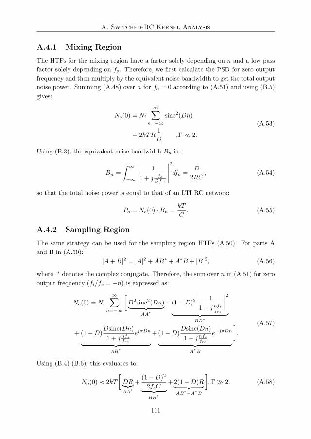
A. Switched-RC Kernel Analysis
A.4.1 Mixing Region
The HTFs for the mixing region have a factor solely depending on n and a low pass
factor solely depending on fo. Therefore, we first calculate the PSD for zero output
frequency and then multiply by the equivalent noise bandwidth to get the total output
noise power. Summing (A.48) over n for fo = 0 according to (A.51) and using (B.5)
gives:
No(0) = Ni
∞∑n=−∞
sinc2(Dn)
= 2kTR1
D,Γ 2.
(A.53)
Using (B.3), the equivalent noise bandwidth Bn is:
Bn =
∫ ∞−∞
∣∣∣∣∣ 1
1 + j foDfrc
∣∣∣∣∣2
dfo =D
2RC, (A.54)
so that the total noise power is equal to that of an LTI RC network:
Po = No(0) ·Bn =kT
C. (A.55)
A.4.2 Sampling Region
The same strategy can be used for the sampling region HTFs (A.50). For parts A
and B in (A.50):
|A+B|2 = |A|2 +AB∗ +A∗B + |B|2, (A.56)
where ∗ denotes the complex conjugate. Therefore, the sum over n in (A.51) for zero
output frequency (fi/fs = −n) is expressed as:
No(0) = Ni
∞∑n=−∞
[D2sinc2(Dn)︸ ︷︷ ︸
AA∗
+ (1−D)2
∣∣∣∣ 1
1− j nfsfrc
∣∣∣∣2︸ ︷︷ ︸BB∗
+ (1−D)Dsinc(Dn)
1 + j nfsfrc
ejπDn︸ ︷︷ ︸AB∗
+ (1−D)Dsinc(Dn)
1− j nfsfrc
e−jπDn︸ ︷︷ ︸A∗B
].
(A.57)
Using (B.4)-(B.6), this evaluates to:
No(0) ≈ 2kT
[DR︸︷︷︸AA∗
+(1−D)2
2fsC︸ ︷︷ ︸BB∗
+ 2(1−D)R︸ ︷︷ ︸AB∗+A∗B
],Γ 2. (A.58)
111

A. Switched-RC Kernel Analysis
Note that for Γ 2 the BB∗ term, contributed by the hold interval, is dominant.
Finding the equivalent noise bandwidths of these terms is complicated because
of the low pass input filter in (A.50). The calculations are made easier by assuming
that:
• Part A is dominated in bandwidth by 1
1+j fofrc,
• Part B is dominated in bandwidth by sinc((1−D)fo/fs),
• The integrated cross terms AB∗ and A∗B are zero.
Part A and part B do not overlap in the time domain, therefore the integrated cross-
power spectrum must be zero according to Parseval’s theorem:∫ ∞−∞
A(f)B∗(f)df =
∫ ∞−∞
a(t)b∗(t)dt = 0. (A.59)
Using (B.2) and (B.3), the noise equivalent bandwidths are:
Bn,AA∗ =
∫ ∞−∞
∣∣∣∣ 1
1 + j fofrc
∣∣∣∣2dfo =1
2RC, (A.60)
and
Bn,BB∗ =
∫ ∞−∞
sinc2
((1−D)
fofs
)dfo =
fs1−D
. (A.61)
So we see that the track interval (Part A) has a lower low-frequency PSD, but a much
higher noise bandwidth than the hold interval (Part B). If we calculate the total noise
power:
Po = No,AA∗ (0) ·Bn,AA∗ +No,BB∗ (0) ·Bn,BB∗
= DkT
C+ (1−D)
kT
C=kT
C,
(A.62)
we find that the total integrated noise is the well known kT/C for sampled-data
systems. It is distributed proportionally to interval length over the track and hold
interval.
112

Appendix B
Integrals and Sums
In this appendix the parameters a and b are real numbers. The sinc function is defined
as:
sinc(x) ≡ sinπx
πx=ejπx − e−jπx
j2πx
sinc(0) = 1, =(sinc(x)) = 0
(B.1)
Integrals using ([72] 3.821 9.) and ([72] 3.112 2.):
∫ ∞−∞
∣∣∣∣1− e−j2πaxj2πx
∣∣∣∣2dx =2
π2
∫ ∞0
sin2(πax)
x2dx = a (B.2)
∫ ∞−∞
∣∣∣∣ 1
1 + jbx
∣∣∣∣2dx =
∫ ∞−∞
1
(1 + jbx)(1− jbx)dx =
π
b(B.3)
Sums using ([72] 1.217 1.), ([72] 0.233) and ([72] 1.443 3.):
∞∑n=−∞
∣∣∣∣ 1
1− jbn
∣∣∣∣2 = 1 + 2
∞∑n=1
1
1 + b2n2=
πb
tanh(πb )
≈ π
b, 0 < b 1
(B.4)
∞∑n=−∞
∣∣∣∣1− e−j2πanj2πn
∣∣∣∣2 = a2 + 2
∞∑n=1
sin2 πan
π2n2
= a2 +1
π2
[ ∞∑n=1
1
n2−∞∑n=1
cos 2πan
n2
]= a
(B.5)
113
B. Integrals and Sums
Sum using ([72] 1.441 1.), ([72] 1.217 1.), ([72] 1.445 2.) and ([72] 1.445 1.):
∞∑n=−∞
ej2πan − 1
j2πn(1 + jbn)=
∞∑n=−∞
(ej2πan − 1)(1 + jbn− jbn)
j2πn(1 + jbn)
=
∞∑n=−∞
ej2πan − 1
j2πn− b
∞∑n=−∞
ej2πan − 1
2π(1 + jbn)
= a+ 2
∞∑n=1
sin(2πan)
2πn+
∞∑n=−∞
b
2π(1 + b2n2)
−∞∑
n=−∞
b cos(2πan)
2π(1 + b2n2)−
∞∑n=−∞
b2n sin(2πan)
2π(1 + b2n2)
=1
2+
1
2· 1 + e−2πb−1
1− e−2πb−1 −e−2πab−1
1− e−2πb−1 , 0 < a < 1
≈ 1, b→ 0
(B.6)
114

Dankwoord
Het uitvoeren en voltooien van een promotie traject, resulterend in een proefschrift,
wordt vaak gezien als een individuele prestatie van de promovendus. In werkelijkheid
is het echter een teamprestatie, waarvan het wel slagen valt of staat met de inbreng
en invloed van de mensen om de promovendus heen. Dit dankwoord is gericht aan
jullie.
Beginnend bij mijn promotor Frank, mijn rots in de branding gedurende het schrij-
ven van dit proefschrift. Jouw overzicht over het grote geheel en aandacht voor de
wetenschappelijke inhoud waren van onschatbare waarde om mijn enthousiaste claims
te temperen en om te vormen naar solide wetenschappelijke bijdragen. Speciale dank
voor mijn dagelijkse begeleider en assistent promotor Eric, voor het doorstaan van
alle energierijke discussies tijdens de projectvergaderingen en het in banen leiden van
het onderzoek. Er is geen mens op deze aarde geduldiger en aandachtiger dan jij.
Voor creatieve inbreng en brainstorming richtte ik mij tot professor Bram N. (a.k.a.
grote Bram). Het is af en toe eng hoe strak wij staan afgesteld op dezelfde golflengte,
waarbij enkele woorden of lijnen op het whiteboard genoeg zijn om de essentie van
een ontwerp over te brengen. Acht jaar geleden was jij degene die mij na een college
Electronic Signal Processing vertelde over geıntegreerde analoge elektronica, dat mo-
ment was voor mij de aanzet om chip-ontwerper te geworden. Het was misschien geen
toeval dat dat gesprek ook al over mixers ging..
Natuurlijk is ondersteuning vanuit de industrie cruciaal voor het afronden van
de chip ontwerpen. Speciale dank voor Domine van NXP voor alle ondersteuning
gedurende de eerste helft van het project, met inbegrip van mijn allereerste ontwerp
review, waar ik alle basis technieken van chip layout heb opgedaan. Many thanks as
well to Andreia of ST Microelectronics, who supported me during the second half of
the project and even offered the hospitality of her home when all hotels were booked
in Grenoble: merci beaucoup.
Zoals alle promovendi weten, zijn het de details die een ontwerp kunnen maken of
breken. Wat ontbreekt in de uiteindelijke presentatie zijn de bloed, zweet en tranen
die vergoten zijn tijdens de late uurtjes van het layout design en de metingen. Daarom
wil ik de aandacht vestigen op het fantastische werk dat gedaan wordt door Henk en
115

Dankwoord
Gerard. Zij zijn degenen die te maken krijgen met alle overblijvende problemen en
zonder hun hulp zouden er geen chips en metingen zijn om over te publiceren.
Naast het serieuze werk is een gezonde dosis humor, afleiding en absurditeit nood-
zakelijk om gezond van geest te blijven. Gelukkig waren deze kwaliteiten in overmate
aanwezig bij mijn kamergenoten bij ICD. Jasper, Johan, Erik, Bram V. (a.k.a. kleine
Bram), Harish, David en Mark: bedankt voor alle zinvolle en zinloze discussies, nach-
telijke uitstapjes en maffe projectjes (vaak eindigend met de kalibratiehamer). Verder
wil ik Gerdien en Annemiek bedanken voor het draaiend houden van de vakgroepen
en het bakje goeie koffie dat ik af en toe mocht bietsen. Natuurlijk ook vele dank
aan mijn andere collega’s bij ICD, SC en TE voor de prettige werkomgeving en leuke
afleidingen zoals diners en barbecues.
Buiten werk om is het ook belangrijk om af en toe stoom af te blazen. Sander,
Niels en Hidde, studiegenoten vanaf het eerste uur, wat hebben we veel lol gehad
in al die jaren. Hoewel we verschillende wegen hebben bewandeld zijn we dan toch
aangekomen bij het eindpunt van onze studies en zullen we nu toch echt moeten
integreren in werkend Nederland. Bedankt voor jullie vriendschap door weer en wind.
Dan nu speciale aandacht voor mijn paranimfen Peter en Gerjan. Naast jullie
ondersteuning tijdens de weekeinden op rij 13, vak 306 in de Grolsch Veste ben ik
vereerd jullie naast mij te hebben staan tijdens de verdediging van dit proefschrift.
We kunnen nu toch duidelijk stellen dat we samen met Berrie en Jouke de juiste
beslissing hebben genomen al die jaren terug om door te gaan met de MEK, met als
gevolg vriendschappen voor het leven. Natuurlijk is ons groepje niet compleet zonder
Erwin, hoe zouden we anders een biertje van het huis krijgen bij eetcafe Jeruzalem?
Dat we samen nog vele shoarma’s mogen proeven.
Ik wil ook de voormalige en huidige bewoners van de MEK bedanken voor alle
gezelligheid en voor het feit dat oud-MEKkers nog steeds hartelijk welkom worden
geheten op de vled (nee, dit is geen typo). De vraag komt wel naar boven of jullie
voortaan zelf de telefoonrekening gaan betalen (knipoog).
Als laatste wil ik mijn hele familie veel dank en liefde toezenden, voor alle onder-
steuning gedurende mijn studie en promotie. Met name mijn ouders voor de stabiele
achtergrond die zij mij hebben gegeven. Marloes, Jarno en Karina, ik bedankt jullie
natuurlijk ook! Ik wil afsluiten door even stil te staan bij de vooruitziende blik van
Opa en Oma Evers. Zij gaven mij als klein jongetje een elektronica experimenteerdoos
op mijn communiefeest. U ziet voor u het resultaat liggen.
116

Bibliography
[1] J. Kilby, “Miniature Electronic Circuits,” US Patent 3 138 743, 1963.
[2] S. Damaraju, V. George, S. Jahagirdar, T. Khondker, R. Milstrey, S. Sarkar,
S. Siers, I. Stolero, and A. Subbiah, “A 22nm IA Multi-CPU and GPU System-
on-Chip,” IEEE ISSCC Dig. Tech. Papers, vol. 55, pp. 56–57, 2012.
[3] International Technology Roadmap for Semiconductors. [Online]. Available:
http://www.itrs.net
[4] R. H. Dennard, F. H. Gaensslen, H. Yu, R. V. Leo, E. Bassous, and A. R. LeBlanc,
“Design of Ion-Implanted MOSFETs with Very Small Physical Dimensions,”
IEEE Journal of Solid-State Circuits, vol. 9, pp. 256–268, Oct. 1974.
[5] L. Zheng and D. N. C. Tse, “Diversity and Multiplexing: A Fundamental Tradeoff
in Multiple-Antenna Channels,” IEEE Trans. on Information Theory, vol. 49,
no. 5, pp. 1073–1096, May. 2003.
[6] T. Paul and T. Ogunfunmi, “Wireless LAN Comes of Age: Understanding the
IEEE 802.11n Amendment,” IEEE Circuits and Systems Magazine, pp. 28–54,
2008.
[7] A. Ghosh, R. Ratasuk, B. Mondal, N. Mangalvedhe, and T. Thomas, “LTE-
Advanced: Next-Generation Wireless Broadband Technology,” IEEE Wireless
Communications, pp. 10–22, Jun. 2010.
[8] J. Paramesh, R. Bishop, K. Soumyanath, and D. J. Allstot, “A 1.4V 5GHz Four-
Antenna Cartesian-Combining Receiver in 90nm CMOS for Beamforming and
Spatial Diversity Applications,” IEEE ISSCC Dig. Tech. Papers, pp. 210–211,
2005.
[9] K. G. Jansky, “Directional Studies of Atmospherics at High Frequencies,” Proc.
of the Institute of Radio Engineers, vol. 20, no. 12, pp. 1920–1932, Dec. 1932.
117
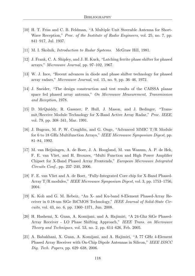
Bibliography
[10] H. T. Friss and C. B. Feldman, “A Multiple Unit Steerable Antenna for Short-
Wave Reception,” Proc. of the Institute of Radio Engineers, vol. 25, no. 7, pp.
841–917, Jul. 1937.
[11] M. I. Skolnik, Introduction to Radar Systems. McGraw Hill, 1981.
[12] J. Frank, C. A. Shipley, and J. H. Kuck, “Latching ferrite phase shifter for phased
arrays,” Microwave Journal, pp. 97–102, 1967.
[13] W. J. Ince, “Recent advances in diode and phase shifter technology for phased
array radars,” Microwave Journal, vol. 15, no. 9, pp. 36–46, 1972.
[14] J. Sneider, “The design construction and test results of the CAISSA planar
space fed phased array antenna,” On Microwave Measurement, Transmission
and Reception, 1978.
[15] D. McQuiddy, R. Gassner, P. Hull, J. Mason, and J. Bedinger, “Trans-
mit/Receive Module Technology for X-Band Active Array Radar,” Proc. IEEE,
vol. 79, pp. 308–341, Mar. 1991.
[16] J. Bugeau, M. P. W. Coughlin, and G. Onge, “Advanced MMIC T/R Module
for 6 to 18 GHz Multifunction Arrays,” IEEE Microwave Symposium Digest, pp.
81–84, 1992.
[17] M. van Heijningen, A. de Boer, J. A. Hoogland, M. van Wanum, A. P. de Hek,
F. E. van Vliet, and H. Brouzes, “Multi Function and High Power Amplifier
Chipset for X-Band Phased Array Frontends,” European Microwave Integrated
Circuits Conf., pp. 237–240, 2006.
[18] F. E. van Vliet and A. de Boer, “Fully-Integrated Core chip for X-Band Phased-
Array T/R modules,” IEEE Microwave Symposium Digest, vol. 3, pp. 1753–1756,
2004.
[19] K. Koh and G. M. Rebeiz, “An X- and Ku-band 8-Element Phased-Array Re-
ceiver in 0.18-um SiGe BiCMOS Technology,” IEEE Journal of Solid-State Cir-
cuits, vol. 43, no. 6, pp. 1360–1371, Jun. 2008.
[20] H. Hashemi, X. Guan, A. Komijani, and A. Hajimiri, “A 24-Ghz SiGe Phased-
Array Receiver - LO Phase Shifting Approach,” IEEE Trans. on Microwave
Theory and Techniques, vol. 53, no. 2, pp. 614–626, Feb. 2005.
[21] A. Babakhani, X. Guan, A. Komijani, and A. Hajimiri, “A 77 GHz 4-Element
Phased Array Receiver with On-Chip Dipole Antennas in Silicon,” IEEE ISSCC
Dig. Tech. Papers, pp. 629–638, 2006.
118
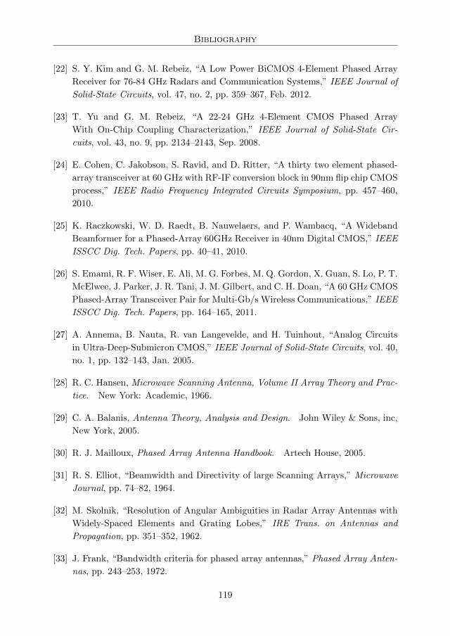
Bibliography
[22] S. Y. Kim and G. M. Rebeiz, “A Low Power BiCMOS 4-Element Phased Array
Receiver for 76-84 GHz Radars and Communication Systems,” IEEE Journal of
Solid-State Circuits, vol. 47, no. 2, pp. 359–367, Feb. 2012.
[23] T. Yu and G. M. Rebeiz, “A 22-24 GHz 4-Element CMOS Phased Array
With On-Chip Coupling Characterization,” IEEE Journal of Solid-State Cir-
cuits, vol. 43, no. 9, pp. 2134–2143, Sep. 2008.
[24] E. Cohen, C. Jakobson, S. Ravid, and D. Ritter, “A thirty two element phased-
array transceiver at 60 GHz with RF-IF conversion block in 90nm flip chip CMOS
process,” IEEE Radio Frequency Integrated Circuits Symposium, pp. 457–460,
2010.
[25] K. Raczkowski, W. D. Raedt, B. Nauwelaers, and P. Wambacq, “A Wideband
Beamformer for a Phased-Array 60GHz Receiver in 40nm Digital CMOS,” IEEE
ISSCC Dig. Tech. Papers, pp. 40–41, 2010.
[26] S. Emami, R. F. Wiser, E. Ali, M. G. Forbes, M. Q. Gordon, X. Guan, S. Lo, P. T.
McElwee, J. Parker, J. R. Tani, J. M. Gilbert, and C. H. Doan, “A 60 GHz CMOS
Phased-Array Transceiver Pair for Multi-Gb/s Wireless Communications,” IEEE
ISSCC Dig. Tech. Papers, pp. 164–165, 2011.
[27] A. Annema, B. Nauta, R. van Langevelde, and H. Tuinhout, “Analog Circuits
in Ultra-Deep-Submicron CMOS,” IEEE Journal of Solid-State Circuits, vol. 40,
no. 1, pp. 132–143, Jan. 2005.
[28] R. C. Hansen, Microwave Scanning Antenna, Volume II Array Theory and Prac-
tice. New York: Academic, 1966.
[29] C. A. Balanis, Antenna Theory, Analysis and Design. John Wiley & Sons, inc,
New York, 2005.
[30] R. J. Mailloux, Phased Array Antenna Handbook. Artech House, 2005.
[31] R. S. Elliot, “Beamwidth and Directivity of large Scanning Arrays,” Microwave
Journal, pp. 74–82, 1964.
[32] M. Skolnik, “Resolution of Angular Ambiguities in Radar Array Antennas with
Widely-Spaced Elements and Grating Lobes,” IRE Trans. on Antennas and
Propagation, pp. 351–352, 1962.
[33] J. Frank, “Bandwidth criteria for phased array antennas,” Phased Array Anten-
nas, pp. 243–253, 1972.
119
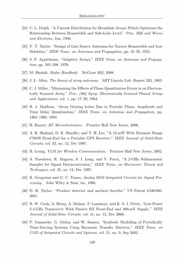
Bibliography
[34] C. L. Dolph, “A Current Distribution for Broadside Arrays Which Optimizes the
Relationship Between Beamwidth and Side-Lobe Level,” Proc. IRE and Waves
and Electrons, Jun. 1946.
[35] T. T. Taylor, “Design of Line Source Antennas for Narrow Beamwidth and Low
Sidelobes,” IEEE Trans. on Antennas and Propagation, pp. 16–28, 1955.
[36] S. P. Applebaum, “Adaptive Arrays,” IEEE Trans. on Antennas and Propaga-
tion, pp. 585–598, 1976.
[37] M. Skolnik, Radar Handbook. McGraw Hill, 2008.
[38] J. L. Allen, The theory of array antennas. MIT Lincoln Lab. Report 323, 1963.
[39] C. J. Miller, “Minimizing the Effects of Phase Quantization Errors in an Electron-
ically Scanned Array,” Proc. 1964 Symp. Electronically Scanned Phased Arrays
and Applications, vol. 1, pp. 17–39, 1964.
[40] R. J. Mailloux, “Array Grating Lobes Due to Periodic Phase, Amplitude and
Time Delay Quantization,” IEEE Trans. on Antennas and Propagation, pp.
1364–1368, 1984.
[41] B. Razavi, RF Microelectronics. Prentice Hall New Jersey, 2006.
[42] A. R. Shahani, D. K. Shaeffer, and T. H. Lee, “A 12-mW Wide Dynamic Range
CMOS Front-End for a Portable GPS Receiver,” IEEE Journal of Solid-State
Circuits, vol. 32, no. 12, Dec 1997.
[43] B. Leung, VLSI for Wireless Communication. Prentice Hall New Jersey, 2002.
[44] A. Parssinen, R. Magoon, S. I. Long, and V. Porra, “A 2-GHz Subharmonic
Sampler for Signal Downconversion,” IEEE Trans. on Microwave Theory and
Techniques, vol. 45, no. 12, Dec 1997.
[45] R. Gregorian and G. C. Temes, Analog MOS Integrated Circuits for Signal Pro-
cessing. John Wiley & Sons, inc, 1986.
[46] D. R. Tayloe, “Product detector and method therefor,” US Patent 6 230 000,
2001.
[47] B. W. Cook, A. Berny, A. Molnar, S. Lanzisera, and K. S. J. Pister, “Low-Power
2.4-GHz Transceiver With Passive RX Front-End and 400-mV Supply,” IEEE
Journal of Solid-State Circuits, vol. 41, no. 12, Dec 2006.
[48] P. Vanassche, G. Gielen, and W. Sansen, “Symbolic Modelling of Periodically
Time-Varying Systems Using Harmonic Transfer Matrices,” IEEE Trans. on
CAD of Integrated Circuits and Systems, vol. 21, no. 9, Sep 2002.
120
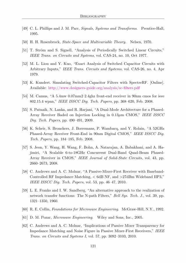
Bibliography
[49] C. L. Phillips and J. M. Parr, Signals, Systems and Transforms. Prentice-Hall,
1995.
[50] H. H. Rosenbrock, State-Space and Multivariable Theory. Nelsen, 1970.
[51] T. Strom and S. Signell, “Analysis of Periodically Switched Linear Circuits,”
IEEE Trans. on Circuits and Systems, vol. CAS-24, no. 10, Oct 1977.
[52] M. L. Liou and Y. Kuo, “Exact Analysis of Switched Capacitor Circuits with
Arbitrary Inputs,” IEEE Trans. Circuits and Systems, vol. CAS-26, no. 4, Apr
1979.
[53] K. Kundert. Simulating Switched-Capacitor Filters with SpectreRF. [Online].
Available: http://www.designers-guide.org/analysis/sc-filters.pdf
[54] M. Camus, “A 5.4mw 0.07mm2 2.4ghz front-end receiver in 90nm cmos for ieee
802.15.4 wpan,” IEEE ISSCC Dig. Tech. Papers, pp. 368–620, Feb. 2008.
[55] S. Patnaik, N. Lanka, and R. Harjani, “A Dual-Mode Architecture for a Phased-
Array Receiver Baded on Injection Locking in 0.13µm CMOS,” IEEE ISSCC
Dig. Tech. Papers, pp. 490–491, 2009.
[56] K. Scheir, S. Bronckers, J. Borremans, P. Wambacq, and Y. Rolain, “A 52GHz
Phased-Array Receiver Front-End in 90nm Digital CMOS,” IEEE ISSCC Dig.
Tech. Papers, pp. 184–185, Feb. 2008.
[57] S. Jeon, Y. Wang, H. Wang, F. Bohn, A. Natarajan, A. Babakhani, and A. Ha-
jimiri, “A Scalable 6-to-18GHz Concurrent Dual-Band Quad-Beam Phased-
Array Receiver in CMOS,” IEEE Journal of Solid-State Circuits, vol. 43, pp.
2660–2673, 2008.
[58] C. Andrews and A. C. Molnar, “A Passive-Mixer-First Receiver with Baseband-
Controlled RF Impedance Matching, < 6dB NF, and >27dBm Wideband IIP3,”
IEEE ISSCC Dig. Tech. Papers, vol. 53, pp. 46–47, 2010.
[59] L. E. Franks and I. W. Sandberg, “An alternative approach to the realization of
network transfer functions: The N-path Filters,” Bell Sys. Tech. J., vol. 39, pp.
1321–1350, 1960.
[60] R. E. Collin, Foundations for Microwave Engineering. McGraw-Hill, N.Y., 1992.
[61] D. M. Pozar, Microwave Engineering. Wiley and Sons, Inc., 2005.
[62] C. Andrews and A. C. Molnar, “Implications of Passive Mixer Transparency for
Impedance Matching and Noise Figure in Passive Mixer-First Receivers,” IEEE
Trans. on Circuits and Systems I, vol. 57, pp. 3092–3103, 2010.
121
Bibliography
[63] A. Mirzaei, H. Darabi, and D. Murphy, “Architectural Evolution of Integrated
M-Phase High-Q Bandpass Filters,” IEEE Trans. Circuits and Systems-I, vol. 59,
no. 1, pp. 52–65, Jan. 2012.
[64] J. Borremans, G. Mandal, V. Giannini, T. Sano, M. Ingels, B. Verbruggen, and
J. Craninckx, “A 40nm CMOS Highly Linear 0.4-to6Ghz Receiver Resilient to
0dBm Out-of-Band Blockers,” IEEE ISSCC Dig. Tech. Papers, pp. 62–63, 2011.
[65] D. Murphy, A. Hafez, A. Mirzaei, M. Mikhemar, H. Darabi, M. F. Chang, and
A. Abidi, “A Blocker-Tolerant Wideband Noise-Cancelling Receiver With a 2 dB
Noise Figure,” IEEE ISSCC Dig. Tech. Papers, pp. 74–75, 2012.
[66] A. Ghaffari, E. A. M. Klumperink, and B. Nauta, “A Differential 4-Path Highly
Linear Widely Tunable On-Chip Band-Pass Filter,” IEEE Radio Frequency In-
tegrated Circuits Symposium, pp. 299–302, 2010.
[67] A. Mirzaei, H. Darabi, A. Yazdi, Z. Zhou, E. Chang, and P. Suri, “A 65nm CMOS
Quad-Band SAW-Less Receiver SoC for GSM/GPRS/EDGE,” IEEE Journal of
Solid-State Circuits, vol. 46, no. 4, pp. 950–964, Apr. 2011.
[68] M. Darvishi, R. van der Zee, E. A. M. Klumperink, and B. Nauta, “A 0.3-
to-1.2GHz Tunable 4-th Order Switched Gm-C Bandpass Filter with > 55dB
Ultimate Rejection and Out-of-Band IIP3 of +29dBm,” IEEE ISSCC Dig. Tech.
Papers, pp. 358–359, 2012.
[69] R. Tseng, H. Li, D. H. Kwon, Y. Chiu, and A. S. Y. Poon, “A Four-Channel
Beamforming Down-Converter in 90-nm CMOS Utilizing Phase-Oversampling,”
IEEE Journal of Solid-State Circuits, vol. 45, no. 11, pp. 2262–2272, Nov. 2010.
[70] B. Cetinoneri, Y. A. Atesal, and G. M. Rebeiz, “An 8 X 8 Butler Matrix in 0.13-
um CMOS for 5-6 GHz Multibeam Applications,” IEEE Trans. on Microwave
Theory and Techniques, vol. 59, no. 2, pp. 295–301, Feb. 2011.
[71] A. Opal and J. Vlach, “Analysis and Sensitivity of Periodically Switched Linear
Networks,” IEEE Trans. on Circuits and Systems, vol. 36, no. 4, Apr 1989.
[72] I. S. Gradshteyn and I. M. Ryzhik, Table of Integrals, Series, and Products,
A. Jeffrey, Ed. Academic Press, 1994.
122
List of Publications
1. M.C.M. Soer, E.A.M. Klumperink, Z. Ru, F.E. van Vliet, B. Nauta, ”A 0.2-
to-2.0GHz 65nm CMOS Receiver Without LNA Achieving >11dBm IIP3 and
<6.5dB NF”, IEEE Solid-State Circuits Conference, Digest of Technical Papers,
pp. 222-223, Feb 2009.
2. M.C.M. Soer, E.A.M. Klumperink, PT de Boer, F.E. van Vliet, B. Nauta,
”Unified Frequency Domain Analysis of Switched-RC Passive Mixers and Sam-
plers”, IEEE Transactions on Circuits and Systems I: Regular Papers, vol. 57,
num. 10, pp. 2618-2631, Oct. 2010.
3. M.S. Oude Alink, E.A.M. Klumperink, M.C.M. Soer, A.B.J. Kokkeler, B.
Nauta, ”A 50MHz-to-1.5GHz Cross-Correlation CMOS Spectrum Analyzer for
Cognitive Radio with 89dB SFDR in 1MHz RBW”, Proc. 4th IEEE Symposium
on New Frontiers in Dynamic Spectrum Access Networks, Singapore, Apr. 2010.
4. M.C.M. Soer, E.A.M. Klumperink, B. Nauta, F.E. van Vliet, ”A 1.0-to-
4.0GHz 65nm CMOS Four-Element Beamforming Receiver Using a Switched-
Capacitor Vector Modulator with Approximate Sine Weighting via Charge Re-
distribution”, IEEE Solid-State Circuits Conference, Digest of Technical Papers,
pp. 64-65, Feb 2011.
5. A. Ghaffari, E.A.M. Klumperink, M.C.M. Soer, B. Nauta, ”Tunable High-Q
N-Path Band-Pass Filters: Modeling and Verification”, IEEE Journal of Solid-
State Circuits, vol. 46, num. 5, pp. 998, May 2011.
6. M.C.M. Soer, E.A.M. Klumperink, B. Nauta, F.E. van Vliet, ”Spatial Inter-
ferer Rejection in a 4-Element Beamforming Receiver Frontend with a Switched-
Capacitor Vector Modulator”, IEEE Journal of Solid-State Circuits, vol.46,
no.12, pp. 2933-2942, Dec. 2011.
123
List of Publications
7. M.S. Oude Alink, E.A.M. Klumperink, A.B.J. Kokkeler, M.C.M. Soer, G.J.M.
Smit, B. Nauta, ”A CMOS-Compatible Spectrum Analyzer for Cognitive Radio
Exploiting Crosscorrelation to Improve Noise and Linearity Performance”, IEEE
Transactions on Circuits and Systems I: Regular Papers, vol. 59, num. 3, pp.
479-492, Mar. 2012.
8. M.C.M. Soer, E.A.M. Klumperink, B. Nauta, F.E. van Vliet, ”A 1.5-to-
5.0GHz Input-Matched +2dBm P1dB All-Passive Switched-Capacitor Beam-
forming Receiver Front-End in 65nm CMOS”, IEEE Solid-State Circuits Con-
ference, Digest of Technical Papers, pp. 174-175, Feb 2012.
9. F.E. van Vliet, E.A.M. Klumperink, M.C.M. Soer, S.K. Garakoui, A. de Boer,
A.P. de Hek, W. de Heij, B. Nauta, ”Advances in Silicon Phased-Array Receiver
IC’s”, IEEE International Microwave Symposium, Digest of Technical Papers,
Jun. 2012.
124

List of Abbreviations
AC Alternating Current
ADC Analog to Digital Converter
CML Current Mode Logic
CMOS Complementary Metal Oxide Semiconductor
DC Direct Current
DI Differential
EM Electro-Magnetic
FET Field Effect Transistor
GaAs Gallium-Arsenide
GaN Gallium-Nitride
HTF Harmonic Transfer Function
IC Integrated Circuit
IEEE Institute of Electrical and Electronics Engineers
IF Intermediate Frequency
IIP3 Input-referred third-order Intercept Point
InP Indium-Phosphide
I/Q In-phase / Quadrature
ISM Industrial Scientific Medical
LNA Low Noise Amplifier
LO Local Oscillator
LP Low Power
LPTV Linear Periodically Time Variant
LTE Long Term Evolution
125

List of Abbreviations
LTI Linear Time Invariant
MIMO Multiple-Input-Multiple-Output
MMIC Monolithic Microwave Integrated Circuits
NF Noise Figure
NMOS N-type Metal Oxide Semiconductor
PCB Printed Circuit Board
PMOS P-type Metal Oxide Semiconductor
PSD Power Spectral Density
RC Resistor-Capacitor
RF Radio Frequency
RMS Root Mean Square
SE Single Ended
SFDR Spurious Free Dynamic Range
SiGe Silicon-Germanium
SNR Signal-to-Noise Ratio
SSB Single Side Band
T/R Transmit / Receive
WLAN Wireless Local Area Network
ZOH Zero-Order Hold
126