Embed Size (px)
Citation preview
You Can’t Miss It
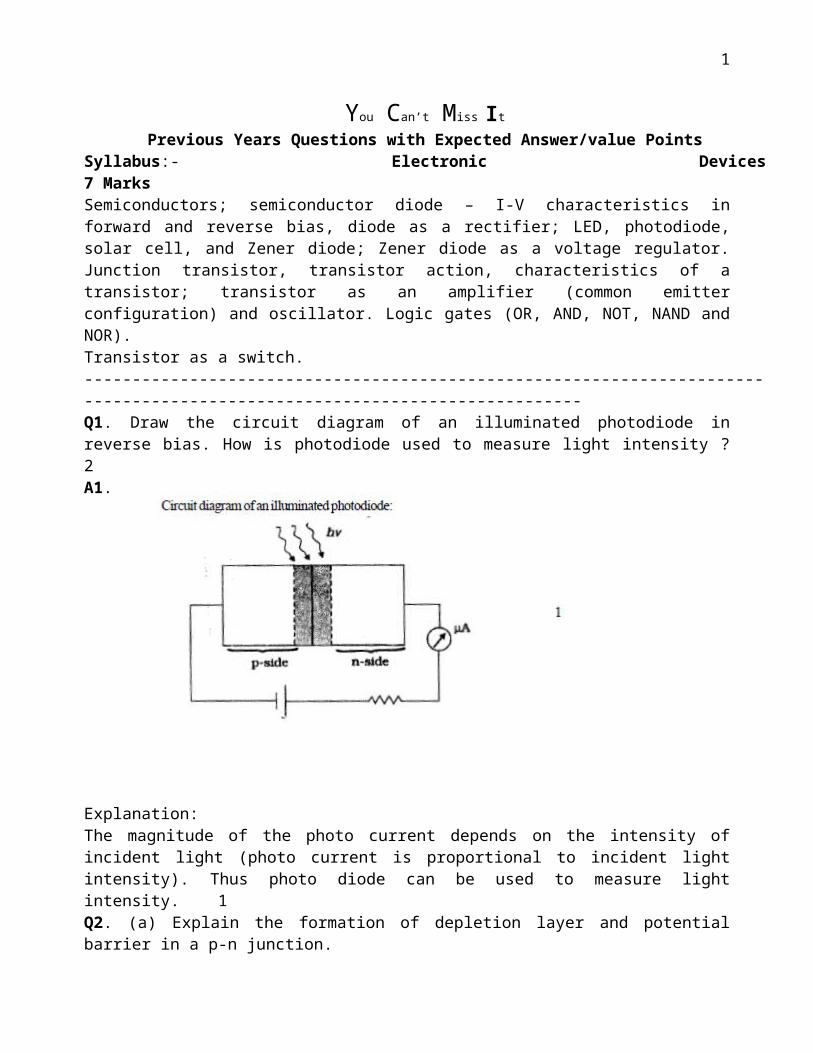
Previous Years Questions with Expected Answer/value PointsSyllabus:- Electronic Devices 7 MarksSemiconductors; semiconductor diode – I-V characteristics in forward and reverse bias, diode as a rectifier; LED, photodiode, solar cell, and Zener diode; Zener diode as a voltage regulator. Junction transistor, transistor action, characteristics of a transistor; transistor as an amplifier (common emitter configuration) and oscillator. Logic gates (OR, AND, NOT, NAND and NOR).Transistor as a switch.---------------------------------------------------------------------------------------------------------------------------Q1. Draw the circuit diagram of an illuminated photodiode in reverse bias. How is photodiode used to measure light intensity ? 2A1.
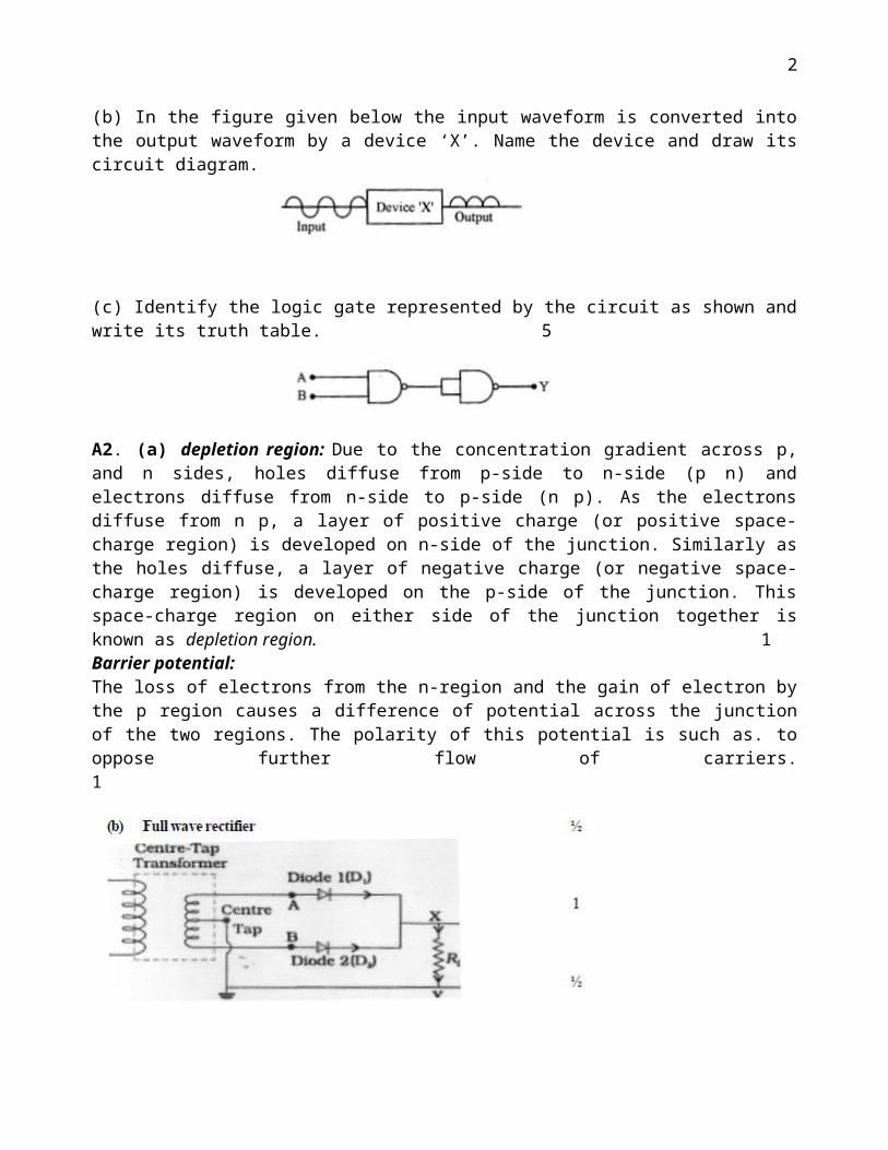
Explanation:The magnitude of the photo current depends on the intensity of incident light (photo current is proportional to incident light intensity). Thus photo diode can be used to measure light intensity. 1Q2. (a) Explain the formation of depletion layer and potential barrier in a p-n junction. (b) In the figure given below the input waveform is converted into the output waveform by a device ‘X’. Name the device and draw its circuit diagram.
(c) Identify the logic gate represented by the circuit as shown and write its truth table. 5
A2. (a) depletion region: Due to the concentration gradient across p, and n sides, holes diffuse from p-side to n-side (p n) and electrons diffuse from n-side to p-side (n p). As the electrons diffuse from n p, a layer of positive charge (or positive space-charge region) is developed on n-side of the junction. Similarly as the holes diffuse, a layer of negative charge (or negative space-charge region)
1
is developed on the p-side of the junction. This space-charge region on either side of the junction together is known as depletion region. 1Barrier potential:The loss of electrons from the n-region and the gain of electron by the p region causes a difference of potential across the junction of the two regions. The polarity of this potential is such as. to oppose further flow of carriers. 1
OR(a) With the help of the circuit diagram explain the working principle of a transistor amplifier as an oscillator.(b) Distinguish between a conductor, a semiconductor and an insulator on the basis of energy band diagrams.A (a)
2
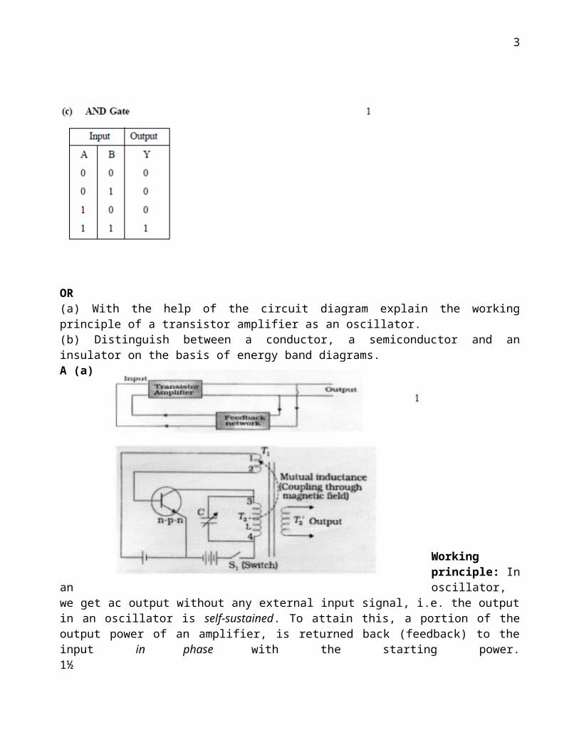
Working principle: In an oscillator, we get ac output without any external input signal, i.e. the output in an oscillator is self-sustained. To attain this, a portion of the output power of an amplifier, is returned back (feedback) to the input in phase with the starting power. 1½
(b) The energy band diagrams, showing the distinction between a conductor, a semiconductor and an insulator are shown below:
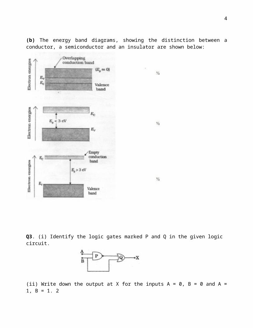
Q3. (i) Identify the logic gates marked P and Q in the given logic circuit.
(ii) Write down the output at X for the inputs A = 0, B = 0 and A = 1, B = 1. 2 A3. (i) P: NAND gate ½ Q: OR gate ½(ii) Inputs A = 0 and B = 0 then output X=1 ½ Inputs A = 1 and B = 1 then output X = 1 ½
½
3
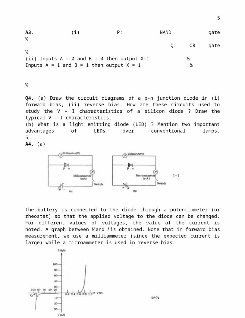
Q4. (a) Draw the circuit diagrams of a p-n junction diode in (i) forward bias, (ii) reverse bias. How are these circuits used to study the V - I characteristics of a silicon diode ? Draw the typical V - I characteristics.(b) What is a light emitting diode (LED) ? Mention two important advantages of LEDs over conventional lamps. 5A4. (a)
The battery is connected to the diode through a potentiometer (or rheostat) so that the applied voltage to the diode can be changed. For different values of voltages, the value of the current is noted. A graph between V and I is obtained. Note that in forward bias measurement, we use a milliammeter (since the expected current is large) while a microammeter is used in reverse bias.
Typical V-I characteristics of a silicon diode.(b) Light emitting diodeIt is a heavily doped p-n junction which under forward bias emits spontaneous radiation./ p-n junction diode which emits light when forwardly biased. 1Advantages:(i) Low operational voltage and less power.(ii) Fast action and no warm-up time required.(iii) The bandwidth of emitted light is 100 A to 500 A , or in other words it is nearly (but not exactly) monochromatic.(iv) Long life and ruggedness.(v) Fast on-off switching capability (Any two) ½+½
4
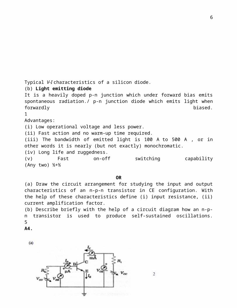
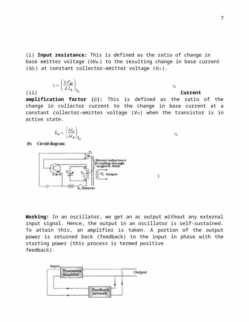
OR(a) Draw the circuit arrangement for studying the input and output characteristics of an n-p-n transistor in CE configuration. With the help of these characteristics define (i) input resistance, (ii) current amplification factor.(b) Describe briefly with the help of a circuit diagram how an n-p-n transistor is used to produce self-sustained oscillations. 5A4.
(i) Input resistance: This is defined as the ratio of change in base emitter voltage (VBE ) to the resulting change in base current (IB ) at constant collector-emitter voltage (VCE ).
(ii) Current amplification factor (): This is defined as the ratio of the change in collector current to the change in base current at a constant collector-emitter voltage (VCE) when the transistor is in active state.
Working: In an oscillator, we get an ac output without any external input signal. Hence, the output in an oscillator is self-sustained. To attain this, an amplifier is taken. A portion of the output power is returned back (feedback) to the input in phase with the starting power (this process is termed positivefeedback).
5
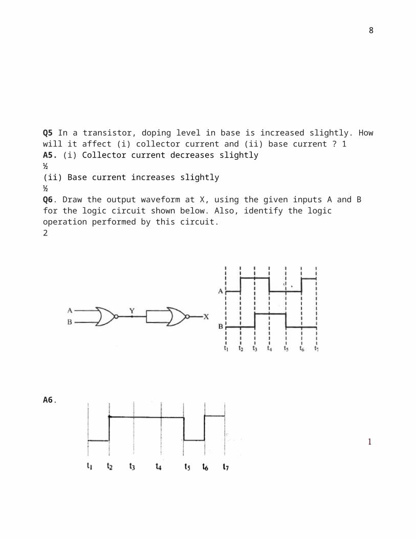
Q5 In a transistor, doping level in base is increased slightly. How will it affect (i) collector current and (ii) base current ? 1A5. (i) Collector current decreases slightly ½(ii) Base current increases slightly ½Q6. Draw the output waveform at X, using the given inputs A and B for the logic circuit shown below. Also, identify the logic operation performed by this circuit. 2
A6.
OR gate 1(However if the outputwavefonn is drawnwrong but the student correctly identifies the logic operation (according to the outputwavefonn drawn) award 1mark only)
6
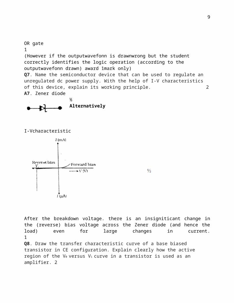
Q7. Name the semiconductor device that can be used to regulate an unregulated dc power supply. With the help of I-V characteristics of this device, explain its working principle. 2
A7. Zener diode ½Alternatively
I-Vcharacteristic
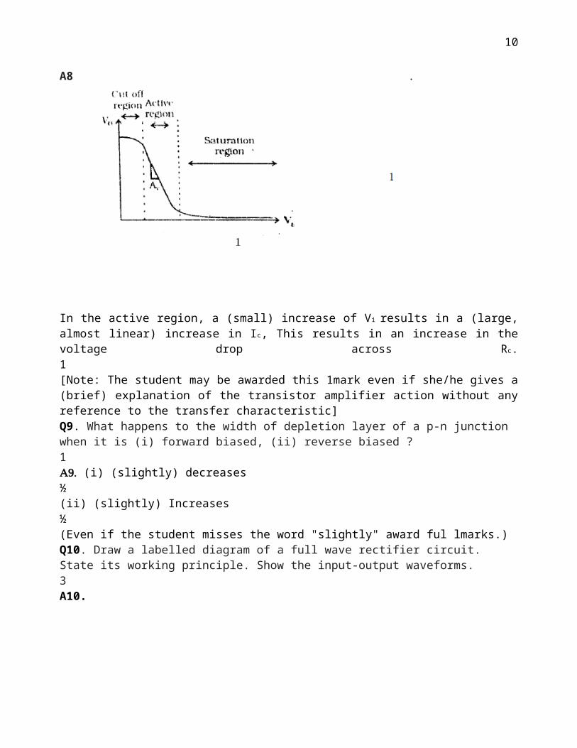
After the breakdown voltage. there is an insigniticant change in the (reverse) bias voltage across the Zener diode (and hence the load) even for large changes in current. 1Q8. Draw the transfer characteristic curve of a base biased transistor in CE configuration. Explain clearly how the active region of the V0 versus Vi curve in a transistor is used as an amplifier. 2A8 .
7
In the active region, a (small) increase of Vi results in a (large, almost linear) increase in Ic, This results in an increase in the voltage drop across Rc. 1[Note: The student may be awarded this 1mark even if she/he gives a (brief) explanation of the transistor amplifier action without any reference to the transfer characteristic]Q9 . What happens to the width of
depletion layer of a p-n junction when it is (i) forward
biased, (ii) reverse biased ?
1 (i) (slightly) decreases
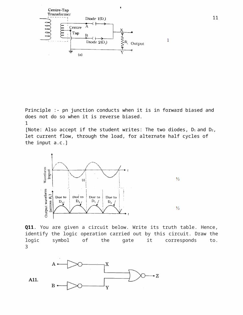
½(ii) (slightly) Increases ½(Even if the student misses the word "slightly" award ful lmarks.)Q10. Draw a labelled diagram of a full wave rectifier circuit. State its working principle. Show the input-output waveforms. 3A10.
Principle :- pn junction conducts when it is in forward biased and does not do so when it is reverse biased. 1[Note: Also accept if the student writes: The two diodes, D1 and D2, let current flow, through the load, for alternate half cycles of the input a.c.]
8
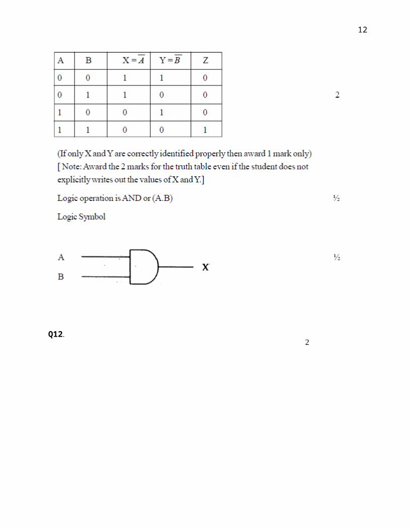
Q11. You are given a circuit below. Write its truth table. Hence, identify the logic operation carried out by this circuit. Draw the logic symbol of the gate it corresponds to. 3
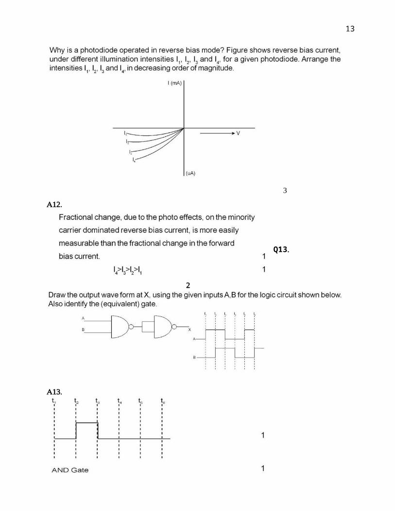
Q12
9
Q13
10
Q
11
Q15
12
A15.
Q16. 5
13
A16.
Q17. 2
14
A17.
Q18. 2
A18.
Q19.
15
A19.
16


![ECT2601 - gimmenotes · Troubleshoot various faults in transistor circuits. ... Common Emitter Amplifier. [p274] Understand and analyze the operation of common emitter amplifiers](https://img.pdfslide.net/doc/110x75/5e90704e877ed1389036c928/ect2601-gimmenotes-troubleshoot-various-faults-in-transistor-circuits-common.jpg)
![BJT or FET Transistor Configurations - MITweb.mit.edu/6.101/www/s2017/handouts/L05_4.pdf · ... Common Emitter Amplifier [b] Common Collector ... complicated circuit using basic properties](https://img.pdfslide.net/doc/110x75/5b1688a87f8b9a5e6d8c7917/bjt-or-fet-transistor-configurations-common-emitter-amplifier-b-common.jpg)