Embed Size (px)
Citation preview
Symbolic Analysis of Large Analog Integrated Circuits: The Numerical Reference Generation Problem2
Symbolic Analysis of Large Analog Integrated Circuits:
The Numerical Reference Generation ProblemFrancisco V. Fernández, Oscar Guerra, Juan D. Rodríguez-García and Angel
Rodríguez-Vázquez
Instituto de Microelectrónica de Sevilla, Centro Nacional de MicroelectrónicaE-41012-Sevilla, SPAIN
Footnote
This work has been supported by the EEC ESPRIT Program in the Framework of the
Project #21812 (AMADEUS) and the Spanish C.I.C.Y.T. under contract TIC97-0580.
Abstract
Symbolic analysis potentialities for gaining circuit insight and for efficient
repetitive evaluations have been limited by the exponential increase of for-
mula complexity with the circuit size. This drawback has began to be solved
by the introduction of simplification before and during generation techniques.
An appropriate error control in both involves the generation of a numerical
reference, which implies the calculation of network functions in the complex
frequency variable. The polynomial interpolation method, traditionally used
for this task, is analyzed in detail, its limitations for large circuit analysis are
pointed out, and an adaptive scaling mechanism is proposed to meet the effi-
ciency and accuracy requirements imposed by the new simplification meth-
odologies.

Symbolic Analysis of Large Analog Integrated Circuits: The Numerical Reference Generation Problem3
I. INTRODUCTION
Symbolic circuit analysis refers to the calculation of network functions where the complex
frequency and all or part of the circuit parameters are symbols. These functions are typically
given in the form:
(1)
where and are sums of products of the symbolic parameters
. See for instance [1] and [2] for an actualized review of techniques and
applications of symbolic analysis.
Plain symbolic analysis suffers from a tremendous increase of expression complexity with
the circuit size. Consider for illustration’s sake the circuits in Fig. 1. The DC voltage gain of
Fig. 1a using the model in Fig. 1b is:
(2)
which contains 21 terms; this number raises to 8616 for the Miller opamp in Fig. 1c using the
model in Fig. 1d, and is well above for theµA741 opamp in Fig. 1e using the model in
Fig. 1f1. Given this exponential increase of the term count with the number of elements in the
circuit model, symbolic expressionsimplification has been recognized to be essential for both:
formula interpretation by human designers and computer manipulation forrepetitive evalua-
tions in design automation applications [1]. For instance, elimination of the least significant
terms in (2) leads to which is a much more interpretable expression.
Conventional simplification approaches first calculate thecomplete symbolic expression,
and then simplify it by eliminating insignificant terms or sub-expressions, based on numerical
estimates of the symbolic parameters—commonly calledSimplification After Generation
(SAG). Consequently, most of the resources employed to generate the pruned terms are wasted.
Besides, although this is a feasible approach for circuits like those of Fig. 1a and c (in general,
1. The number of terms for Fig. 1c was obtained using ASAP [3] while the lower bound of the number ofterms for Fig. 1e was calculated using the theory presented in [4].
H s x,( )
sif i x( )
i 0=
N
∑
sjgj x( )
j 0=
M
∑----------------------------=
f i x( ) gj x( )
xTx1 x2 … xQ, , ,{ }=
vo
vi----- gm1gm2rπ1rπ2R3RL R1 R2+( ) R1RL R3 rπ2+( )gm1rπ1 R1RL R3 rπ2+( )+ +[ ] ⁄=
gm1gm2rπ1rπ2R3RLR1 gm1rπ1 R2 RL+( ) R3 rπ2+( )R1 R2 RL+( ) R3 rπ2+( ) R1 rπ1+( ) R3 rπ2+( )+ rπ1R1]+ +[
1016
vo
vi-----
R1 R2+( )R1
-----------------------≈
Symbolic Analysis of Large Analog Integrated Circuits: The Numerical Reference Generation Problem4
for circuits with less than around 50 symbols), it is unfeasible for circuits like that in Fig. 1e, as
no computer has enough memory to handle such a huge number of symbolic terms, on the one
hand, and the time needed to generate them would not be affordable, on the other. These larger
circuits have to be analyzed by using the newest approaches:Simplification DuringGeneration
(SDG) andSimplification BeforeGeneration (SBG). This paper deals with a basic ingredient of
these new techniques, namely the generation of a numerical reference to evaluate the errors in
the simplification process. Based on a brief description of our implementation of SBG and SDG
(Section II), Section III addresses the generation of this reference, describing the problems aris-
ing when handling medium and large size analog integrated circuits and introducing new algo-
rithms for its efficient calculation. Experimental results are shown in Section IV.
II. THE APPROXIMATION METHODOLOGY
A. Simplification During Generation
SDG techniques start from some formulation of the network equations and solve them try-
ing to directly generate the simplified expression. In our SDG approach, symbolic terms are
generated in decreasing order of magnitude until the generated terms represent a significant
fraction of the complete expression.
The first reliable algorithms capable of efficiently generating terms in decreasing order of
magnitude [5]-[8] were based on thetwo-graph method [9]. The computation of the simplified
coefficients ofsk reduces to the following problem: “Given the voltage graphGV and the current
graphGI of a circuit withn nodes, enumerate subsets of branches in decreasing order of
magnitude such that: (a) form a spanning tree inGV ; (b) form a spanning tree inGI ; and, (c)
containk capacitances and (trans)conductances”. This problem can be formulated
in terms ofmatroids [10]. Each condition (a)−(c) above is mapped into a matroid and the prob-
lem of generation of common spanning trees in order is mapped into a weighted matroid inter-
section problem. The algorithms in [5]-[8] calculate the intersection of two matroids among
(a)-(c) [11], and then check if it intersects the third matroid. Although the intersection problem
of three general matroids is nonpolynomial-hard, [12], [13] have reported the first algorithm
able to solve it by exploiting the characteristics of the three particular matroids at hand. These
algorithms have made feasible the analysis of large circuits like theµA741 opamp in a few tens
of seconds.
An important ingredient of SDG is the error criterion used to stop the generation of terms.
Consider that represents eitherfi(x) or gj(x) in (1). TheP most significant
n 1–( )
n k– 1–( )
hk x( ) hkl x( )l 1=
T
∑=
Symbolic Analysis of Large Analog Integrated Circuits: The Numerical Reference Generation Problem5
terms are generated in until the sum of the generated terms represents a given fraction of
the total magnitude of the coefficient,
(3)
wherexo represents a design point of the circuit parameters andεk is an error control parameter
which is obtained by backpropagation from maximum magnitude and phase error specifica-
tions. As shown in (3), the total magnitude of each circuit coefficient, , must be known
a priori; however, the fully symbolic expression is not available for such calculation. Hence, an
efficient technique able to calculate (1) with onlys as symbolic variable is needed. The problems
arising in this calculation when handling large circuits are addressed in Section III.
Once an approximated expression has been calculated, the maximum magnitude
and phase errors with respect to the exact expression in a given frequency range can be
obtained from:
(4)
where
(5)
The application of interval analysis techniques [14] to (4) to evaluate the maximum mag-
nitude and phase errors in a given frequency range usually yields overly conservative estimates
of those maxima. Therefore, interval analysis techniques are applied to the derivatives of (4) to
delimit frequency subranges in which the maximum magnitude and phase errors occur. Then,
the frequency points for which the maximum magnitude or phase error occurs in those fre-
quency subranges are easily calculated using the Newton-Raphson method.
hk x( )
hk xo( ) hkl xo( )l 1=
P
∑– εk hk xo( )<
hk xo( )
Hap s( )
Hex s( )
ε H
Hex jω( ) Hap jω( )–
Hex jω( )------------------------------------------------------ 1
Napr2
Napi2
+
Dapr2
Dapi2
+----------------------------
Nexr2
Nexi2
+
Dexr2
Dexi2
+---------------------------
---------------------------------–= =
∆φH Hex jω( ) Hap jω( )∠–∠Nexi
Nexr-----------atan
Dexi
Dexr----------atan–
Napi
Napr-----------
Dapi
Dapr-----------atan+atan–= =
Hap jω( )Nap jω( )Dap jω( )---------------------
Napr ω( ) jNapi ω( )+
Dapr ω( ) jDapi ω( )+--------------------------------------------------= =
Hex jω( )Nex jω( )Dex jω( )---------------------
Nexr ω( ) jNexi ω( )+
Dexr ω( ) jDexi ω( )+-------------------------------------------------= =
Symbolic Analysis of Large Analog Integrated Circuits: The Numerical Reference Generation Problem6
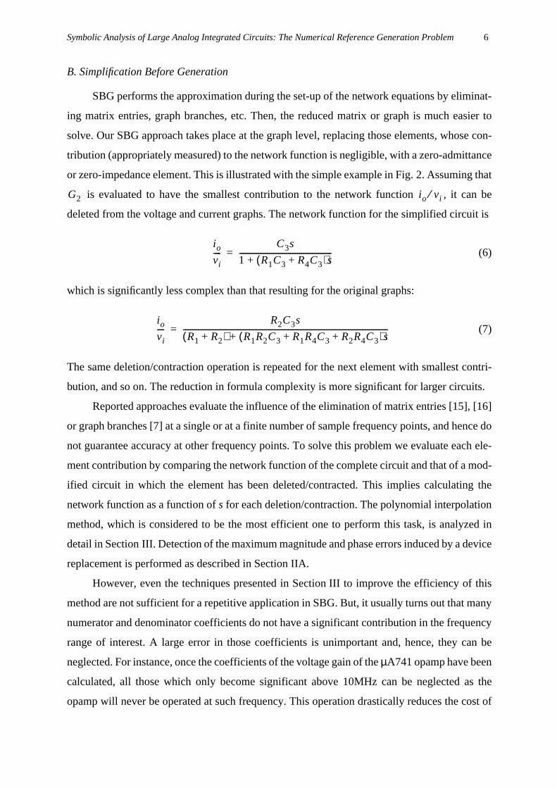
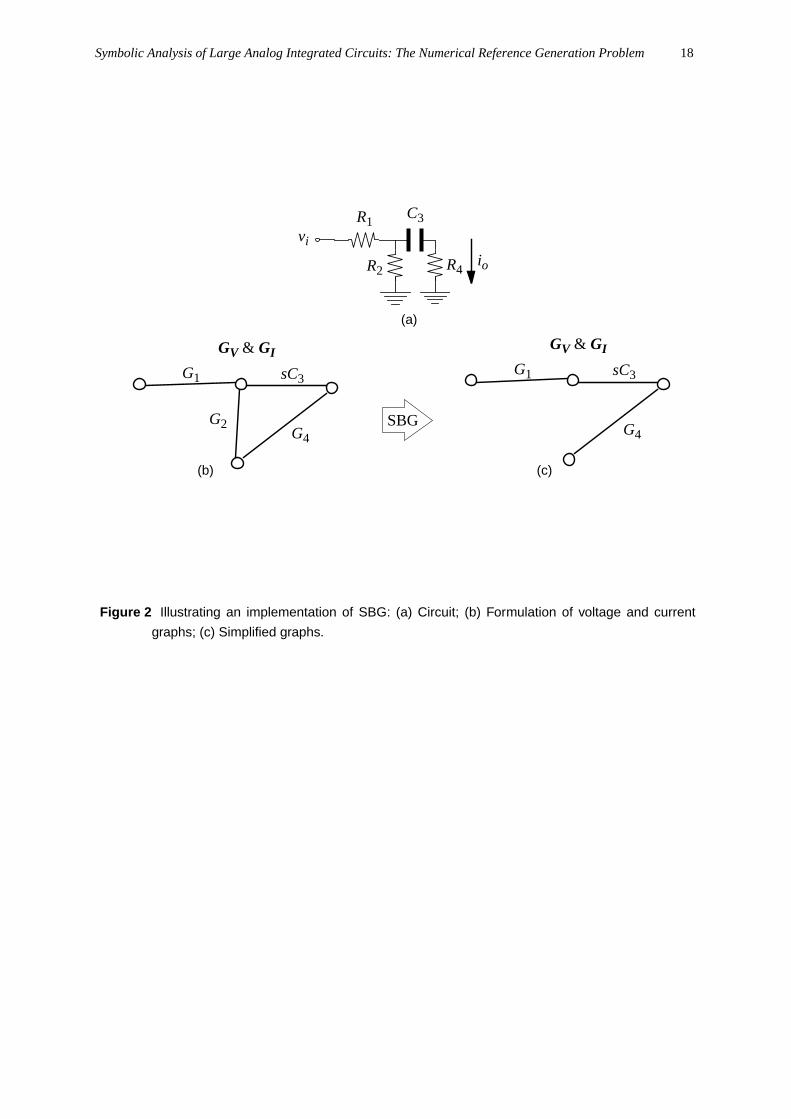
B. Simplification Before Generation
SBG performs the approximation during the set-up of the network equations by eliminat-
ing matrix entries, graph branches, etc. Then, the reduced matrix or graph is much easier to
solve. Our SBG approach takes place at the graph level, replacing those elements, whose con-
tribution (appropriately measured) to the network function is negligible, with a zero-admittance
or zero-impedance element. This is illustrated with the simple example in Fig. 2. Assuming that
is evaluated to have the smallest contribution to the network function , it can be
deleted from the voltage and current graphs. The network function for the simplified circuit is
(6)
which is significantly less complex than that resulting for the original graphs:
(7)
The same deletion/contraction operation is repeated for the next element with smallest contri-
bution, and so on. The reduction in formula complexity is more significant for larger circuits.
Reported approaches evaluate the influence of the elimination of matrix entries [15], [16]
or graph branches [7] at a single or at a finite number of sample frequency points, and hence do
not guarantee accuracy at other frequency points. To solve this problem we evaluate each ele-
ment contribution by comparing the network function of the complete circuit and that of a mod-
ified circuit in which the element has been deleted/contracted. This implies calculating the
network function as a function ofs for each deletion/contraction. The polynomial interpolation
method, which is considered to be the most efficient one to perform this task, is analyzed in
detail in Section III. Detection of the maximum magnitude and phase errors induced by a device
replacement is performed as described in Section IIA.
However, even the techniques presented in Section III to improve the efficiency of this
method are not sufficient for a repetitive application in SBG. But, it usually turns out that many
numerator and denominator coefficients do not have a significant contribution in the frequency
range of interest. A large error in those coefficients is unimportant and, hence, they can be
neglected. For instance, once the coefficients of the voltage gain of theµA741 opamp have been
calculated, all those which only become significant above 10MHz can be neglected as the
opamp will never be operated at such frequency. This operation drastically reduces the cost of
G2 io vi⁄
iovi----
C3s
1 R1C3 R4C3+( )s+-------------------------------------------------=
iovi----
R2C3s
R1 R2+( ) R1R2C3 R1R4C3 R2R4C3+ +( )s+-------------------------------------------------------------------------------------------------------------=
Symbolic Analysis of Large Analog Integrated Circuits: The Numerical Reference Generation Problem7
subsequent network function calculations as the polynomial interpolation cost grows with the
number of network function coefficients.
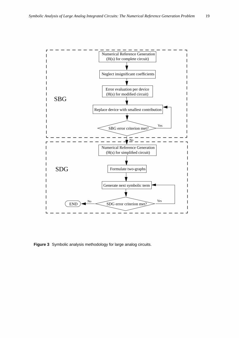
The flow diagram of the complete symbolic analysis methodology including SBG and
SDG is shown in Fig. 3. It must be noticed that the SBG step makes the SDG task much more
effective but it is not essential, that is, SDG can do the work without a previous SBG step.
III. NETWORK FUNCTIONS IN s
Section II has shown that error evaluation in both, SBG and SDG techniques, requires
repetitive calculation of network functions withs as the unique symbolic variable for complete
or reduced circuit models. This establishes how important is to develop efficient calculation
techniques of network functions of medium and large size circuits. The polynomial interpola-
tion method is considered to be one of the most efficient techniques to perform this task [9],[17].
A. Background on polynomial interpolation
The polynomial interpolation starts from the fact that the coefficients of an-th order poly-
nomial,
(8)
can be obtained from the polynomial values at (n+1) distinct points . If these values can
be calculated, then the following matrix equation can be formulated:
(9)
The matrix in (9) is nonsingular and hence (9) has always a unique solution. Such solution is
the set of polynomial coefficients,pi, in (8).
It has been shown that the use of equally-spaced interpolation points in the unit
circle gives the best results concerning numerical accuracy and stability [9], [17]. Once the val-
ues of (8) at all these pointsP(sk) are known, the polynomial coefficients can be obtained
through theDiscrete Fourier Transform (DFT),
P s( ) p0 p1s p2s2 … pns
n+ + + +=
P sk( )
1 s0 s02 … s0
n
1 s1 s12 … s1
n
…
1 sn sn2 … sn
n
p0
p1
…pn
P s0( )
P s1( )
…P sn( )
=
K n 1+≥
Symbolic Analysis of Large Analog Integrated Circuits: The Numerical Reference Generation Problem8
(10)
where
(11)
The number of interpolation points,K, should be at least (n+1), but in most cases, like that
we are dealing with, the polynomial ordern is not known beforehand. Hence, an upper estimate
onK must be done, and (10) should be identically 0 for those coefficients over then-th power.
Our objective is not the calculation of a polynomial but a network function, which is given
by the ratio of two polynomials. Therefore, the polynomial interpolation method is applicable
to our problem once the values of the numerator and denominator at the different
interpolation points are known. In order to calculate and assume that an appro-
priate formulation method, i.e. modified nodal analysis, has been applied on the circuit so that
the network equations can be written as:
(12)
where is the modified nodal matrix,X contains nodal voltages and auxiliary currents, and
E accounts for the influence of the independent sources. Once any frequency-dependent element
in is evaluated at the interpolation points=sk, the value of the network function
(13)
can be obtained by applying LU decomposition and backsubstitution to (12). The denominator
of the network function is easily obtained as:
(14)
and the numerator is easily obtained from (13) and (14):
(15)
B. Introducing scaling
One major problem in polynomial interpolation applied to analog integrated circuits is the
p̂i1K---- P sk( )e
2πikK
-----------–
k 0=
K 1–
∑= i 0 1 … K 1–, , ,=
p̂i
pi
0
=for i n≤otherwise
N sk( ) D sk( )
N sk( ) D sk( )
YMNAX E=
YMNA
YMNA
H sk( )N sk( )D sk( )--------------=
D sk( ) YMNA sk( )=
N sk( )
N sk( ) H sk( ) D sk( )⋅=
Symbolic Analysis of Large Analog Integrated Circuits: The Numerical Reference Generation Problem9
dramatic effect of round-off errors, due to the finite precision arithmetics of computers. The cal-
culation of the differential voltage gain as a function ofs in the positive feedback OTA of
Fig. 4a with the transistor model in Fig. 4b shows these problems. The order of this network
function is unknown a priori, but an upper bound of the order can be estimated at 9; hence 10
interpolation points are used. The interpolated numerator and denominator coefficients when
using interpolation points located at the unit circle are given in Table 1.
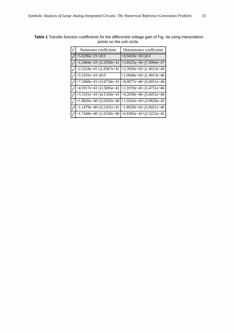
Polynomial coefficients must be real, but, as shown in Table 1, many interpolated coeffi-
cients have a non-zero imaginary component. This is due to the round-off errors, which avoid
perfect cancellations of the imaginary parts in the DFT. The values of these imaginary compo-
nents give us an idea of the numerical noise level induced by the finite number of bits available
in a digital computer to represent the floating point numbers. The real and imaginary parts of
the interpolated coefficients in Table 1, except the two shadowed ones, are of the same order of
magnitude; therefore, the actual value of those coefficients is not obtained as it is below the
numerical error level. Also, as indicated by (11) the zero coefficients would indicate the actual
polynomial order, but as shown in Table 1 the zero coefficients are not detected now.
The numerical error level in the polynomial interpolation depends on the coefficientpi in
(8) having the largest absolute value. This error level is about in a computer
with 16-decimal-digit accuracy [17],[18]. The spread of values between the maximum and min-
imum coefficient should be well below this error to ensure numerical accuracy of the calculated
coefficients:
(16)
Hence, it is not difficult to see that the second and higher order coefficients in Table 1 are not
valid.
Each polynomial coefficient in typical analog integrated circuits is a sum-of-products of
admittances: (trans)conductances and capacitances. Therefore, the coefficient of has one
more (trans)conductance and one less capacitance in each term than the coefficient of .
Taking into account the typical magnitudes of (trans)conductances and capacitances in analog
circuits we can expect an extremely large spread of coefficient values. In order to reduce it, the
complex frequency variable (equivalently the capacitor values) should be scaled before per-
forming the polynomial interpolation on the unit circle [18]. Also, this suggests conductance
scaling as another alternative.
10 13– maxi pi×
mini coefficientimaxi coefficienti------------------------------------------ 10
13–»
si
si 1+

Symbolic Analysis of Large Analog Integrated Circuits: The Numerical Reference Generation Problem10
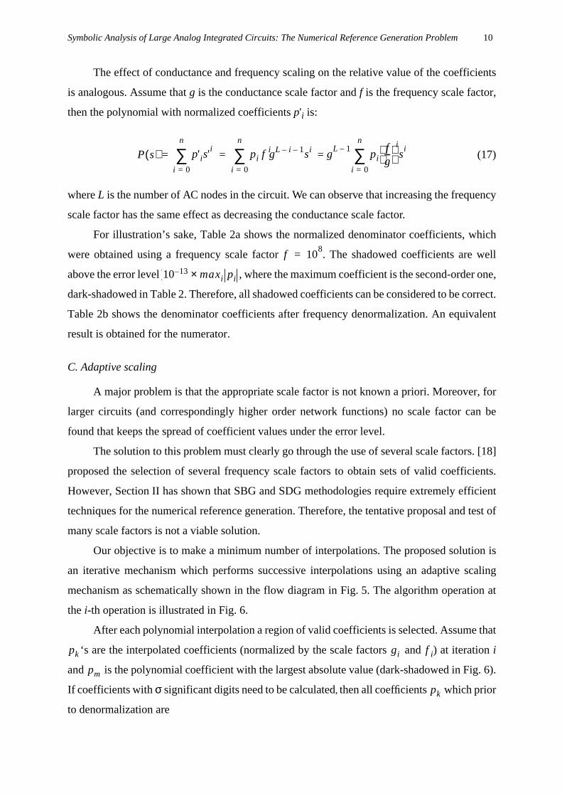
The effect of conductance and frequency scaling on the relative value of the coefficients
is analogous. Assume thatg is the conductance scale factor andf is the frequency scale factor,
then the polynomial with normalized coefficientsp'i is:
(17)
whereL is the number of AC nodes in the circuit. We can observe that increasing the frequency
scale factor has the same effect as decreasing the conductance scale factor.
For illustration’s sake, Table 2a shows the normalized denominator coefficients, which
were obtained using a frequency scale factor . The shadowed coefficients are well
above the error level , where the maximum coefficient is the second-order one,
dark-shadowed in Table 2. Therefore, all shadowed coefficients can be considered to be correct.
Table 2b shows the denominator coefficients after frequency denormalization. An equivalent
result is obtained for the numerator.
C. Adaptive scaling
A major problem is that the appropriate scale factor is not known a priori. Moreover, for
larger circuits (and correspondingly higher order network functions) no scale factor can be
found that keeps the spread of coefficient values under the error level.
The solution to this problem must clearly go through the use of several scale factors. [18]
proposed the selection of several frequency scale factors to obtain sets of valid coefficients.
However, Section II has shown that SBG and SDG methodologies require extremely efficient
techniques for the numerical reference generation. Therefore, the tentative proposal and test of
many scale factors is not a viable solution.
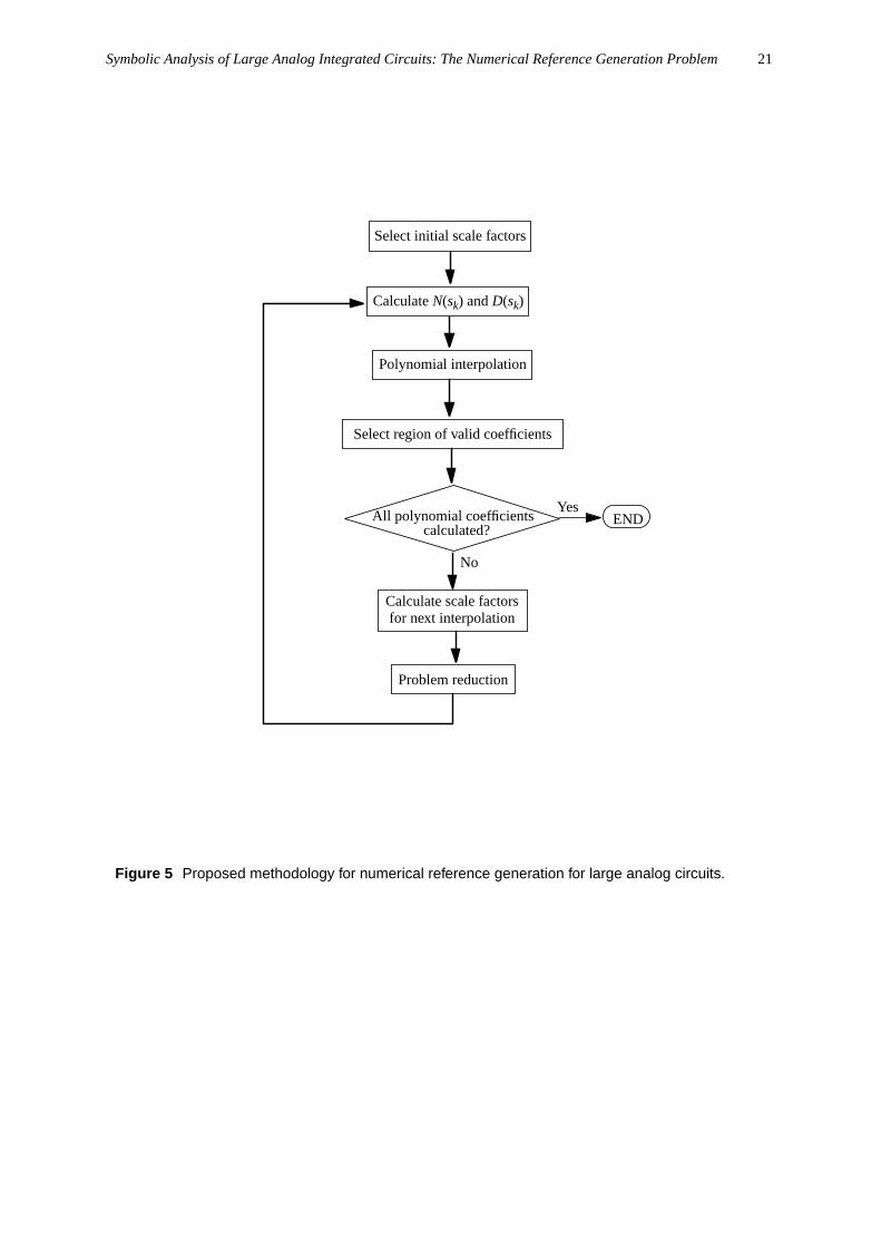
Our objective is to make a minimum number of interpolations. The proposed solution is
an iterative mechanism which performs successive interpolations using an adaptive scaling
mechanism as schematically shown in the flow diagram in Fig. 5. The algorithm operation at
the i-th operation is illustrated in Fig. 6.
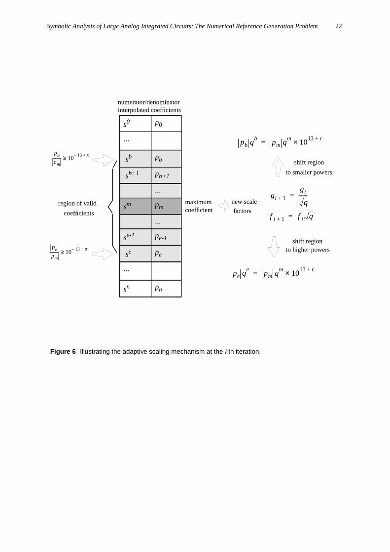
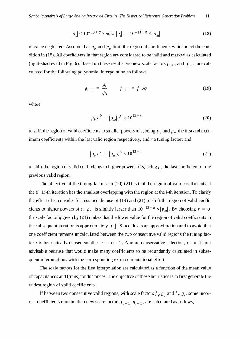
After each polynomial interpolation a region of valid coefficients is selected. Assume that
‘s are the interpolated coefficients (normalized by the scale factors and ) at iterationi
and is the polynomial coefficient with the largest absolute value (dark-shadowed in Fig. 6).
If coefficients withσ significant digits need to be calculated, then all coefficients which prior
to denormalization are
P s( ) p'i s'i
i 0=
n
∑ pi f igL i– 1– si
i 0=
n
∑ gL 1–
pifg---
is
i
i 0=
n
∑= = =
f 108
=
10 13– maxi pi×(
pk gi f i
pm
pk

Symbolic Analysis of Large Analog Integrated Circuits: The Numerical Reference Generation Problem11
(18)
must be neglected. Assume that and limit the region of coefficients which meet the con-
dition in (18). All coefficients in that region are considered to be valid and marked as calculated
(light-shadowed in Fig. 6). Based on these results two new scale factors and are cal-
culated for the following polynomial interpolation as follows:
(19)
where
(20)
to shift the region of valid coefficients to smaller powers ofs, being and the first and max-
imum coefficients within the last valid region respectively, andr a tuning factor; and
(21)
to shift the region of valid coefficients to higher powers ofs, beingpe the last coefficient of the
previous valid region.
The objective of the tuning factorr in (20)-(21) is that the region of valid coefficients at
the (i+1)-th iteration has the smallest overlapping with the region at thei-th iteration. To clarify
the effect ofr, consider for instance the use of (19) and (21) to shift the region of valid coeffi-
cients to higher powers ofs. is slightly larger than . By choosing
the scale factorq given by (21) makes that the lower value for the region of valid coefficients in
the subsequent iteration is approximately . Since this is an approximation and to avoid that
one coefficient remains uncalculated between the two consecutive valid regions the tuning fac-
tor r is heuristically chosen smaller: . A more conservative selection, , is not
advisable because that would make many coefficients to be redundantly calculated in subse-
quent interpolations with the corresponding extra computational effort
The scale factors for the first interpolation are calculated as a function of the mean value
of capacitances and (trans)conductances. The objective of these heuristics is to first generate the
widest region of valid coefficients.
If between two consecutive valid regions, with scale factors , and , , some incor-
rect coefficients remain, then new scale factors , , are calculated as follows,
pk 10 13– σ+ maxi pi×< 10 13– σ+ pm×=
pb pe
f i 1+ gi 1+
gi 1+
gi
q-------= f i 1+ f i q=
pb qb
pm qm
1013 r+×=
pb pm
pe qe
pm qm
1013 r+×=
pe 10 13– σ+ pm× r σ=
pe
r σ 1–= r σ«
f j gj f l gl
f i 1+ gi 1+
Symbolic Analysis of Large Analog Integrated Circuits: The Numerical Reference Generation Problem12
(22)
Notice that in the algorithm above simultaneous scaling of both, frequency and conduc-
tance is used. This technique is used to avoid using too large (>~1018) frequency or conductance
scale factors. These high values occasionally occur when using a single scale factor and are
responsible for an increase of the error in the calculation of numerator and denominator of the
transfer function at the interpolation points.
D. Problem reduction mechanism
In each polynomial interpolation the computational effort depends on the number of inter-
polation frequencies needed. The problem complexity can be reduced at subsequent iterations
of previous algorithm, once the coefficients of the highest or smallest powers ofs have been
calculated. Assume the coefficientsp0...pk−1 andpl+ 1...pn have already been calculated, then the
polynomial is transformed as follows,
(23)
The new polynomial contains the coefficients that still have to be calculated and needs only
l−k+1 interpolation points. This simple operation drastically reduces the computation time at
subsequent iterations.
IV. EXPERIMENTAL RESULTS
The proposed algorithm is applied in this section to two examples: the analysis of the
µA741 opamp and a bandpass biquad described at the transistor level.
A. TheµA741 opamp
Consider the voltage gain of theµA741 opamp in Fig. 1e with the small-signal BJT model
of Fig. 1f. The results of the polynomial interpolation with the first frequency and conductance
scale factors are partially shown in Table 3. The imaginary parts of the coefficients have been
omitted from Table 3 as they originate from the numerical noise in the DFT. According to (18),
the region of valid denominator coefficients is determined from the coefficient with largest nor-
malized absolute value (dark-shadowed in Table 3): . If 6 significant digits are desired all
denominator coefficients larger than
f i 1+ f j f l⋅= gi 1+ gj gl⋅=
P' s( ) pk … pl sl k–⋅+ +
P s( ) pi si⋅
i 0=
k 1–
∑– pi si⋅
i l 1+=
n
∑–
sk
---------------------------------------------------------------------------= =
p3
Symbolic Analysis of Large Analog Integrated Circuits: The Numerical Reference Generation Problem13
(24)
are considered correct. That means that the region of valid denominator coefficients extends
from to (light-shadowed). The remaining coefficients are not shown in Table 3 as it lacks
interest. As indicated by (13)-(15) numerator and denominator coefficients are obtained simul-
taneously with a minimum extra cost. Hence, a region of valid numerator coefficients is also
determined analogously.
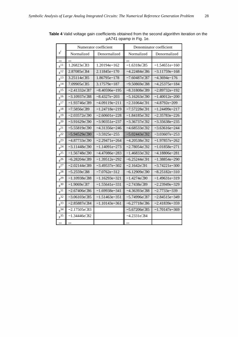
The results of the first interpolation are used to calculate new scale factors and able
to provide a region of valid coefficients of higher powers ofs. For this, (19) and (21) are applied
using and . The problem reduction given by (23) allows the use of 13 less
interpolation points in the next polynomial interpolation. The generated coefficients are shown
in Table 4. The maximum absolute value coefficient, , and the application of (18) delimits
again the region of valid coefficients, which, as shown in Table 4, has shifted to the region
between the 12-th and the 34-th coefficient of the denominator. It can be seen that the overlap
between the valid region in Table 3 and Table 4 reduces to one coefficient in the denominator
and there is no overlap in the numerator.
Again, (19) and (21) are applied to the coefficients in Table 4 to get a new set of scale
factors for higher order coefficients. The problem reduction mechanism reduces in 22 less inter-
polation points for the third (last) iteration of the algorithm. The remaining coefficients,
obtained in the third polynomial interpolation, are shown in Table 5. In this case there is an over-
lap of two coefficients in numerator and denominator.
The CPU time to get the results in this example was 3.9s for the first iteration, 2.3s for the
second one and 0.9s for the third one (measured on a SPARC Station 10). The decrease in the
number of interpolation points due to the problem reduction mechanism is clearly reflected in
a CPU time reduction at subsequent iterations.
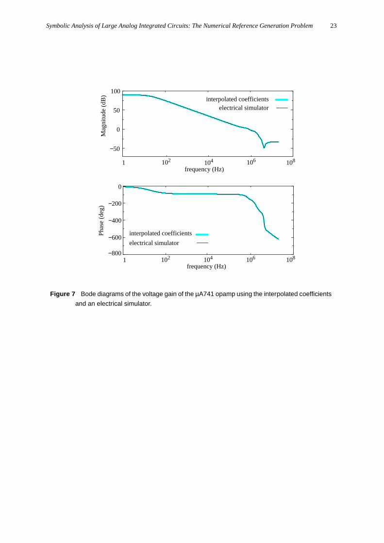
The accuracy of the results obtained in this example is demonstrated through the compar-
ison of the Bode diagrams obtained from the interpolation of numerator and denominator of the
voltage gain ofµA741 and those obtained through a commercial electrical simulator, which are
shown in Fig. 7. A perfect matching appears in all the frequency range.
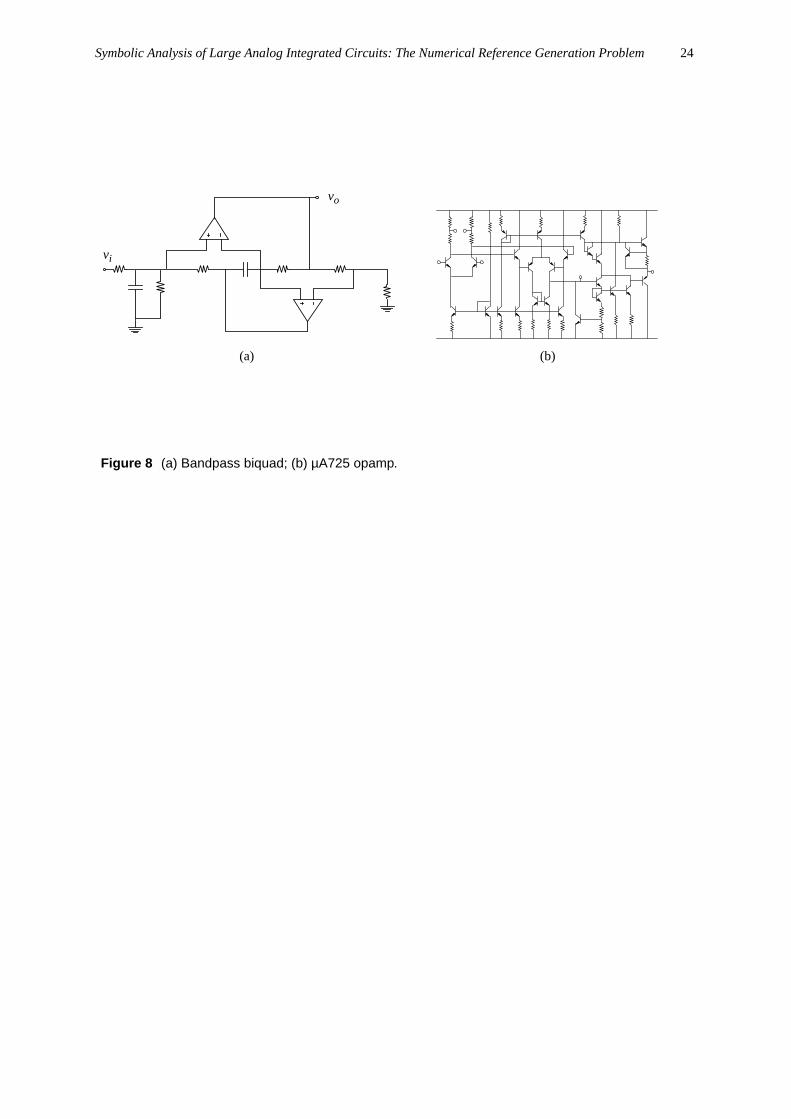
B. Bandpass biquad
As a second example consider the bandpass biquad in Fig. 8a with the opamps described
at the transistor level, as shown in Fig. 8b. The small-signal model used for the bipolar transis-
tors was the same as for the previous example, shown in Fig. 1f. For limited space reasons and
10 13– 6+ 1.28095 124×10× 1.28095 117×10=
p0 p12
f 2 g2
pe p12= pm p3=
p22
Symbolic Analysis of Large Analog Integrated Circuits: The Numerical Reference Generation Problem14
without loss of generality we will limit ourselves to the calculation of the denominator of the
voltage gain of the biquad.
The polynomial interpolation with the first set of frequency and conductance scale factors
provides a region of valid coefficients which extends from the 25-th to the 59-th coefficient, as
shown in Table 6a. To shift the region of valid coefficients to smaller powers of the frequency,
(19) and (20) are applied to the results of the first interpolation. No problem reduction can be
performed at this iteration. However, for the scale factors used the coefficients above the 59-th
one are smaller than the error level. With the new scale factors shifting the valid region to
smaller powers ofs, the influence of the coefficients above the 59-th one on the polynomial
value will be still smaller, and, hence, can be neglected. Neglecting these high order coefficients
is useful because it allows to handle the polynomial as of smaller order, reducing in this way the
number of points needed in the interpolation.
The polynomial interpolation with the new set of scale factors gives a region of valid coef-
ficients which extends from the second to the 24-th coefficient and is shown in Table 6b. The
calculation of the first coefficient, which is under the numerical error level, does not need an
additional polynomial interpolation but a single LU decomposition with no frequency-depen-
dent element in the circuit.
Then, the first 60 denominator coefficients are available, the problem is reduced, and,
hence, 60 less interpolation points are needed at the following iteration. Now, the region of valid
coefficients must be shifted to higher powers ofs; so, (19) and (21) are applied to the results of
the first iteration of the algorithm. A new polynomial interpolation gives the results shown in
Table 6c, where the region of valid coefficients is light-shadowed in Table 6c and its limits have
been determined by (18). Again, the results of this interpolation are used to calculate new scale
factors to shift the region of valid coefficients to higher powers ofs, and to reduce the number
of interpolation points at the following iteration. A new polynomial interpolation gives finally
the remaining denominator coefficients, shown in Table 6d.
The CPU time spent to get the results shown in Table 6 is 30s. This time rises to 80s in
case the problem reduction mechanism is not used. It could be argued that the CPU time
obtained in these examples is acceptable for SDG where the network function ins must be cal-
culated only once, while it is still too high for SBG where the polynomial interpolation or net-
work function calculation might need to be calculated hundredths of times. This is not
commonly true as for real circuits the results of the first network function calculation can be
used to neglect a large number of coefficients for the frequency range in which we are inter-

Symbolic Analysis of Large Analog Integrated Circuits: The Numerical Reference Generation Problem15
ested. That means that the number of interpolation points and, hence, the CPU time, is drasti-
cally reduced for the following executions of the algorithm.
V. CONCLUSIONS
This paper has addressed the problems arising in the calculation of the numerical refer-
ences, essential for an accurate error control in the proposed Simplification Before and During
Generation approach for symbolic analysis of large analog circuits. The proposed algorithm is
based on the polynomial interpolation method and incorporates simultaneous frequency and
conductance scaling, an adaptive updating of the scale factors, and a problem reduction mech-
anism to speed up the generation of the numerical references. The experimental results obtained
with large real-life circuits demonstrate the practical applicability of the techniques introduced
in the paper.
VI. REFERENCES
[1] F.V. Fernández, A. Rodríguez-Vázquez, J.L. Huertas and G. Gielen, eds.,Symbolic Analysis Techniquesand Applications to Analog Design Automation. Piscataway, NJ: IEEE Press, 1998.
[2] G. Gielen, P. Wambacq and W. Sansen, “Symbolic analysis methods and applications for analog circuits: Atutorial overview,”Proc. of the IEEE, vol. 82, no. 2, pp. 287-304, February 1994.
[3] F. V. Fernández, A. Rodríguez-Vázquez, J. D. Martín, and J. L. Huertas, “Formula approximation for flatand hierarchical symbolic analysis,” Analog Integrated Circuits and Signal Processing, vol. 3, no. 1,pp. 43−58, January 1993.
[4] M. Swamy and K. Thulasiraman,Graphs, Networks and Algorithms. New York: John Wiley and Sons,1981.
[5] F.V. Fernández, P. Wambacq, G. Gielen, A. Rodríguez-Vázquez and W. Sansen, “Symbolic analysis oflarge analog integrated circuits by approximation during expression generation,”Proc. IEEE Int. Symp.Circuits and Systems, vol. CAD, pp. 25-28, 1994.
[6] P. Wambacq, F.V. Fernández, G. Gielen, W. Sansen and A. Rodríguez-Vázquez, “Efficient symbolic com-putation of approximated small-signal characteristics of analog integrated circuits,”IEEE J. Solid-StateCircuits, vol. 30, no. 3, pp. 327-330, March 1995.
[7] Q. Yu and C. Sechen, “Approximate symbolic analysis of large analog integrated circuits,”Proc. IEEE Int.Conf. Computer-Aided Design, pp. 664-671, 1994.
[8] Q. Yu and C. Sechen, “Efficient approximation of symbolic network functions using matroid intersectionalgorithms,”Proc. IEEE Int. Symp. Circuits Systems, pp. 2088−2091, 1995.
[9] P.M. Lin, Symbolic Network Analysis. Amsterdam: Elsevier, 1991.
[10] E. L. Lawler,Combinatorial Optimization: Networks and Matroids. New York: Holt, Rinehart and Win-ston, 1976.
[11] P.M. Camerini and H.W. Hamacher, “Intersection of two matroids: (condensed) border graph and rank-ing”, SIAM J. Discrete Mathematics, vol. 2, pp. 16-27, February 1989.

Symbolic Analysis of Large Analog Integrated Circuits: The Numerical Reference Generation Problem16
[12] M. Galán, I. García-Vargas, F.V. Fernández and A. Rodríguez-Vázquez, “A new matroid intersection algo-rithm for symbolic large circuit analysis,”Proc. Workshop on Symbolic Methods and Applications to Cir-cuit Design, Leuven, Belgium, 1996.
[13] M. Galán, F.V. Fernández and A. Rodríguez-Vázquez, “Comparison of matroid intersection algorithms forlarge circuit analysis,”Proc. IEEE Int. Symp. Circuits and Systems, pp. 1784-1787, 1997.
[14] R. E. Moore,Methods and Applications of Interval Analysis. Studies in Applied Mathematics, Philadel-phia, 1979.
[15] Jer-Jaw Hsu and C. Sechen, "Fully symbolic analysis of large analog integrated circuits,"Proc. IEEE Cus-tom Integrated Circuits Conf., pp. 21.4.1−21.4.4, 1994.
[16] R. Sommer, E. Hennig, G. Droge, and E.-H. Horneber, “Equation-based symbolic approximation bymatrix reduction with quantitative error prediction,”Alta Frequenza, vol. 5, no. 6, pp. 317−325, November1993.
[17] J. Vlach and K. Singhal,Computer Methods for Circuit Analysis and Design. Van Nostrand Reinhold,1994.
[18] K. Singhal and J. Vlach, “Generation of immittance functions in symbolic form for lumped distributedactive networks,”IEEE Trans. Circuits and Systems, vol. CAS-21, no. 1, pp. 57-67, January 1974.

Symbolic Analysis of Large Analog Integrated Circuits: The Numerical Reference Generation Problem17
Figure 1 (a) BJT feedback amplifier; (b) low-frequency BJT model; (c) Miller operational amplifier;
(d) MOSFET model; (e) µA741 operational amplifier; (f) BJT model.
R2
R3
R1
RLvi
vo
Q1
Q2
(a)
vi+vi− vo
vi− vi+
(b)
(c)
voB ’
E
CgmvBErπ goCπ
Cµrb rµB
D
BG
S
gmvgsgmbvbsgds
CsbCgs
Cgd Cdb
(d)
(e)
E
CgmvBErπ
B
(f)
Symbolic Analysis of Large Analog Integrated Circuits: The Numerical Reference Generation Problem18
R2 R4
R1vi
io
C3
G1
G2
sC3
G4
GV & GI
Figure 2 Illustrating an implementation of SBG: (a) Circuit; (b) Formulation of voltage and current
graphs; (c) Simplified graphs.
G1 sC3
G4
GV & GI
SBG
(a)
(b) (c)
Symbolic Analysis of Large Analog Integrated Circuits: The Numerical Reference Generation Problem19
Numerical Reference Generation
Neglect insignificant coefficients
Error evaluation per device
Replace device with smallest contribution
SBG error criterion met?
Formulate two-graphs
Generate next symbolic term
SDG error criterion met?
Figure 3 Symbolic analysis methodology for large analog circuits.
(H(s) for complete circuit)
(H(s) for modified circuit)
Numerical Reference Generation(H(s) for simplified circuit)
Yes
No
YesNoEND
SBG
SDG

Symbolic Analysis of Large Analog Integrated Circuits: The Numerical Reference Generation Problem20
vi+ vi−
Vdd
Vss
voGm Gm
Figure 4 (a) Positive feedback OTA; (b) MOSFET model.
D
BG
S
gmvgsgmbvbsgds
CsbCgs
Cgd Cdb
(b)
(a)
Symbolic Analysis of Large Analog Integrated Circuits: The Numerical Reference Generation Problem21
Select region of valid coefficients
No
YesEND
Polynomial interpolation
All polynomial coefficients calculated?
Calculate scale factorsfor next interpolation
Problem reduction
Figure 5 Proposed methodology for numerical reference generation for large analog circuits.
CalculateN(sk) andD(sk)
Select initial scale factors
Symbolic Analysis of Large Analog Integrated Circuits: The Numerical Reference Generation Problem22
s0 p0
...
sb pb
sb+1 pb+1
...
sm pm
...
se-1 pe-1
se pe
...
sn pn
Figure 6 Illustrating the adaptive scaling mechanism at the i-th iteration.
pb qb
pm qm
1013 r+×=
gi 1+
gi
q-------=
f i 1+ f i q=
pe qe
pm qm
1013 r+×=
pb
pm--------- 10
13– σ+≥
pe
pm--------- 10
13– σ+≥
region of valid
coefficients
new scale
factors
numerator/denominatorinterpolated coefficients
shift region
to smaller powers
shift regionto higher powers
maximumcoefficient
Symbolic Analysis of Large Analog Integrated Circuits: The Numerical Reference Generation Problem23
1 102 104 106 108
frequency (Hz)
−50
0
50
100
Mag
nitu
de (
dB)
1 102 104 106 108
frequency (Hz)
−800
−600
−400
−200
0
Pha
se (
deg)
Figure 7 Bode diagrams of the voltage gain of the µA741 opamp using the interpolated coefficients
and an electrical simulator.
interpolated coefficients
electrical simulator
interpolated coefficientselectrical simulator
Symbolic Analysis of Large Analog Integrated Circuits: The Numerical Reference Generation Problem24
Figure 8 (a) Bandpass biquad; (b) µA725 opamp.
(a) (b)
vi
vo
Symbolic Analysis of Large Analog Integrated Circuits: The Numerical Reference Generation Problem25
Table 1 Transfer function coefficients for the differential voltage gain of Fig. 4a using interpolationpoints on the unit circle.
si Numerator coefficients Denominator coefficients
s0 −5.8296e−25+j0.0 +8.9418e−30+j0.0
s1 −1.5484e−33−j2.2958e−41 +3.8525e−36−j7.0064e−47
s2 −2.5254e−41+j1.8367e−41 +2.3920e−43−j1.4013e−46
s3 −5.5101e−41+j0.0 +1.0646e−43−j1.4013e−46
s4 +7.3468e−41+j3.6734e−41 −8.4077e−46−j5.6051e−46
s5 −4.5917e−41+j3.5695e−41 +2.1019e−45−j5.4751e−46
s6 +5.5101e−41+j4.1326e−41 −4.2039e−46−j5.6051e−46
s7 +1.8826e−40−j2.0203e−40 +1.0243e−43+j3.0828e−45
s8 −1.1479e−40+j5.5101e−41 −1.8020e−43−j5.6051e−46
s9 −1.7448e−40−j1.6530e−40 +6.8383e−43+j2.5223e−45

Symbolic Analysis of Large Analog Integrated Circuits: The Numerical Reference Generation Problem26
Table 2 Denominator coefficients for the differential voltage gain of Fig. 4a using afrequency scale factor .
si (a) Normalized coefficients (b) Denormalized coefficients
s0 8.94186e−30−j5.74242e−44 8.94186e−30−j5.74242e−44
s1 3.85259e−28+j1.39200e−44 3.85259e−36+j1.39200e−52
s2 4.20423e−27+j8.17887e−43 4.20423e−43+j8.17887e−59
s3 1.31933e−27+j3.12804e−43 1.31933e−51+j3.12804e−67
s4 1.69136e−28−j2.85774e−43 1.69136e−60−j2.85774e−75
s5 1.09681e−29−j3.09269e−43 1.09681e−69−j3.09269e−83
s6 3.58708e−31−j4.41609e−43 3.58708e−79−j4.41609e−91
s7 4.72362e−33+j2.45089e−43 4.72362e−89+j2.45089e−99
s8 9.71439e−42−j6.61683e−43 9.71439e−106−j6.61683e−107
s9 −7.50537e−42−j2.6935e−42 −7.50537e−114−j2.6935e−114
f 108
=

Symbolic Analysis of Large Analog Integrated Circuits: The Numerical Reference Generation Problem27
Table 3 Valid voltage gain coefficients obtained from the first algorithm iteration on theµA741 opamp in Fig. 1e.
siNumerator coefficients Denominator coefficients
Normalized Denormalized Normalized Denormalized
s0 −9.60926e+122 −5.58675e−86 −2.82408e+118 −1.6419e−90
s1 −1.05987e+124 −2.10393e−91 −7.32222e+122 −1.45352e−92
s2 −1.48757e+124 −1.00824e−97 −8.26327e+123 −5.60064e−98
s3 −1.09256e+124 −2.52835e−104 −1.28095e+124 −2.96432e−104
s4 −4.74222e+123 −3.74701e−111 −1.20867e+124 −9.55018e−111
s5 −1.20465e+123 −3.24992e−118 −7.46903e+123 −2.015e−117
s6 −1.7316e+122 −1.59502e−125 −3.17468e+123 −2.92428e−124
s7 −1.17059e+121 −3.68155e−133 −9.73518e+122 −3.06176e−131
s8 3.98904e+119 4.28355e−141 −2.19449e+122 −2.3565e−138
s9 2.12204e+119 7.7803e−148 −3.61682e+121 −1.32608e−145
s10 3.16408e+118 3.96094e−155 −4.2945e+120 −5.37606e−153
s11 2.81205e+117 1.20194e−162 −3.61821e+119 −1.54651e−160
s12 1.45161e+116 ... −2.13624e+118 −3.11759e−168
s13 3.74942e+114 ... −8.7689e+116 ...
... ... ...
s48 ...
Symbolic Analysis of Large Analog Integrated Circuits: The Numerical Reference Generation Problem28
Table 4 Valid voltage gain coefficients obtained from the second algorithm iteration on theµA741 opamp in Fig. 1e.
siNumerator coefficient Denominator coefficient
Normalized Denormalized Normalized Denormalized
... ... ...
s11 1.26823e+83 1.20194e−162 −1.6318e+85 −1.54651e−160
s12 2.87085e+84 2.11845e−170 −4.22484e+86 −3.11759e−168
s13 3.25114e+85 1.86795e−178 −7.60487e+87 −4.3694e−176
s14 7.09905e+85 3.17579e−187 −9.50869e+88 −4.25375e−184
s15 −2.41332e+87 −8.40596e−195 −8.31808e+89 −2.89732e−192
s16 −3.10937e+88 −8.4327e−203 −5.16263e+90 −1.40012e−200
s17 −1.93746e+89 −4.09119e−211 −2.31064e+91 −4.8792e−209
s18 −7.5856e+89 −1.24718e−219 −7.57228e+91 −1.24499e−217
s19 −2.03572e+90 −2.60601e−228 −1.84185e+92 −2.35783e−226
s20 −3.91629e+90 −3.90351e−237 −3.36737e+92 −3.35638e−235
s21 −5.55819e+90 −4.31356e−246 −4.68533e+92 −3.63616e−244
s22 −5.94529e+90 −3.5925e−255 −5.02443e+92 −3.03607e−253
s23 −4.87733e+90 −2.29471e−264 −4.20538e+92 −1.97857e−262
s24 −3.11448e+90 −1.14091e−273 −2.78054e+92 −1.01858e−271
s25 −1.56748e+90 −4.47086e−283 −1.46833e+92 −4.18806e−281
s26 −6.28204e+89 −1.39512e−292 −6.25244e+91 −1.38854e−290
s27 −2.02144e+89 −3.49537e−302 −2.1642e+91 −3.74221e−300
s28 −5.2559e+88 −7.0762e−312 −6.12909e+90 −8.25182e−310
s29 −1.10938e+88 −1.16293e−321 −1.4274e+90 −1.49631e−319
s30 −1.9069e+87 −1.55641e−331 −2.7438e+89 −2.23949e−329
s31 −2.67406e+86 −1.69938e−341 −4.36393e+88 −2.7733e−339
s32 −3.06103e+85 −1.51463e−351 −5.74996e+87 −2.84515e−349
s33 −2.85887e+84 −1.10143e−361 −6.27718e+86 −2.41839e−359
s34 −2.17505e+83 −5.67206e+85 −1.70147e−369
s35 −1.34446e+82 −4.2331e+84
... ... ...

Symbolic Analysis of Large Analog Integrated Circuits: The Numerical Reference Generation Problem29
Table 5 Valid voltage gain coefficients obtained from the third algorithm iterationon the µA741 opamp in Fig. 1e.
siNumerator coefficient Denominator coefficient
Normalized Denormalized Normalized Denormalized
... ... ...
s31 −9.54531e+100 −1.69938e−341 −1.55775e+103 −2.7733e−339
s32 −1.31048e+102 −1.51463e−351 −2.46167e+104 −2.84515e−349
s33 −1.46792e+103 −1.10143e−361 −3.2231e+105 −2.41839e−359
s34 −1.33944e+104 −6.52456e−372 −3.49298e+106 −1.70147e−369
s35 −9.93e+104 −3.14017e−382 −3.12651e+107 −9.88697e−380
s36 −5.95853e+105 −1.22326e−392 −2.30357e+108 −4.72912e−390
s37 −2.87924e+106 −3.83736e−403 −1.39051e+109 −1.85323e−400
s38 −1.11283e+107 −9.62853e−414 −6.83395e+109 −5.91294e−411
s39 −3.40957e+107 −1.91517e−424 −2.7127e+110 −1.52373e−421
s40 −8.18174e+107 −2.98352e−435 −8.6082e+110 −3.13903e−432
s41 −1.51217e+108 −3.57981e−446 −2.15541e+111 −5.10259e−443
s42 −2.10129e+108 −3.2294e−457 −4.18739e+111 −6.43546e−454
s43 −2.11603e+108 −2.11122e−468 −6.17333e+111 −6.1593e−465
s44 −1.45292e+108 −9.41084e−480 −6.70084e+111 −4.34028e−476
s45 −6.06159e+107 −2.54889e−491 −5.12766e+111 −2.15617e−487
s46 −1.15315e+107 −3.14794e−503 −2.58524e+111 −7.05735e−499
s47 −7.60583e+110 −1.34792e−510
s48 −9.74782e+109 −1.1215e−522
Symbolic Analysis of Large Analog Integrated Circuits: The Numerical Reference Generation Problem30
Table 6 Valid denominator coefficients of the voltage gain of the bandpass biquad in Fig. 8aobtained from the (a) first, (b) second, (c) third and (d) fourth algorithm iteration.
si(a) Denominator coefficients
si(b) Denominator coefficients
Normalized Denormalized Normalized Denormalized
... ... s0 −3.91876e+56
s23 −7.51056e+09 s1 −1.01152e+58−4.94769e−230
s24 −5.94246e+10 s2 −7.75231e+59−4.44594e−235
s25 −7.29364e+11−5.2904e−395 ... ... ...
... ... ... s8 −1.04737e+64−1.56051e−272
s40 −5.80151e+18−3.26183e−513 s9 −1.42046e+64−2.48143e−279
s41 −6.87954e+18−1.70385e−521 s10 −1.56628e+64−3.2081e−286
s42 −7.2521e+18 −7.91199e−530 s11 −1.4507e+64 −3.48388e−293
s43 −6.79335e+18−3.2648e−538 s12 −1.163e+64 −3.2747e−300
... ... ... ... ... ...
s58 −1.47487e+12−3.23433e-670 s23 −2.94228e+60−4.76909e−380
s59 −8.03012e+11−1.96111e−679 s24 −8.74623e+59−1.66218e−387
... s25 ...calculated...
si(c) Denominator coefficients
si(d) Denominator coefficients
Normalized Denormalized Normalized Denormalized
s59 ...calculated... s87 ...calculated...
s60 −3.64197e+12−1.05641e−688 s88 ...calculated...
... ... ... s89 −9.84964e+47−3.47589e−978
s68 −1.03089e+15−1.183e−764 ... ... ...
s69 −1.26356e+15−2.2963e−774 s94 −5.04429e+49−3.76528e−1032
s70 −1.39033e+15−4.00138e−784 s95 −7.39434e+49−4.04545e−1043
s71 −1.37471e+15−6.2656e−794 s96 −9.31988e+49−3.73721e−1054
... ... ... s97 −1.00029e+50−2.9399e−1065
s86 −4.32544e+09−1.94841e−946 s98 −9.03506e+49−1.9463ε−1076
s87 −7.99215e+08−5.70129e−957 ... ... ...
s88 −1.41979e+08−1.49098e−967 s104 −3.93227e+47−1.31324e−1145
s89 −1.94284e+07 s105 −4.561e+46 −1.11642e−1157
... ... ... s106 −2.41567e+45−4.33388e−1170

Symbolic Analysis of Large Analog Integrated Circuits: The Numerical Reference Generation Problem31
LIST OF FIGURESFigure 1 (a) BJT feedback amplifier; (b) low-frequency BJT model; (c) Miller operational amplifier; (d)
MOSFET model; (e) mA741 operational amplifier; (f) BJT model.
Figure 2 Illustrating an implementation of SBG: (a) Circuit; (b) Formulation of voltage and current
graphs; (c) Simplified graphs.
Figure 3 Symbolic analysis methodology for large analog circuits.
Figure 4 (a) Positive feedback OTA; (b) MOSFET model.
Figure 5 Proposed methodology for numerical reference generation for large analog circuits.
Figure 6 Illustrating the adaptive scaling mechanism at the i-th iteration.
Figure 7 Bode diagrams of the voltage gain of the µA741 opamp using the interpolated coefficients
and an electrical simulator.
Figure 8 (a) Bandpass biquad; (b) µA725 opamp.

Symbolic Analysis of Large Analog Integrated Circuits: The Numerical Reference Generation Problem32
LIST OF TABLES Table 1 Transfer function coefficients for the differential voltage gain of Fig. 4a using interpolation
points on the unit circle. Table 2 Denominator coefficients for the differential voltage gain of Fig. 4a using a frequency scale
factor. Table 3 Valid voltage gain coefficients obtained from the first algorithm iteration on the µA741 opamp
in Fig. 1e. Table 4 Valid voltage gain coefficients obtained from the second algorithm iteration on the µA741
opamp in Fig. 1e. Table 5 Valid voltage gain coefficients obtained from the third algorithm iteration on the µA741 opamp
in Fig. 1e. Table 6 Valid denominator coefficients of the voltage gain of the bandpass biquad in Fig. 8a obtained
from the (a) first, (b) second, (c) third and (d) fourth algorithm iteration.

Symbolic Analysis of Large Analog Integrated Circuits: The Numerical Reference Generation Problem33
FOOTNOTES
1. The number of terms for Fig. 1c was obtained using ASAP [3] while the lower bound of thenumber of terms for Fig. 1e was calculated using the theory presented in [4].
Symbolic Analysis of Large Analog Integrated Circuits: The Numerical Reference Generation Problem1
Symbolic Analysis of Large Analog Integrated Circuits:
The Numerical Reference Generation Problem
Francisco V. Fernández, Oscar Guerra, Juan D. Rodríguez-García and Angel
Rodríguez-Vázquez
Instituto de Microelectrónica de Sevilla - Centro Nacional de MicroelectrónicaAvda. Reina Mercedes s/n, (Edif. CICA)
E-41012, Sevilla, Spain
IEEE Transactions on Circuits and Systems - II,Accepted for publication to appear in 1998
© 1998 IEEE. Personal use of this material is permitted. However, permission to reprint/republish this materialfor advertising or promotional purposes or for creating new collective works for resale or redistribution to serversor lists, or to reuse any copyrighted component of this work in other works must be obtained from the IEEE.
This material is presented to ensure timely dissemination of scholarly and technical work. Copyright and allrights therein are retained by authors or by other copyright holders. All persons copying this information areexpected to adhere to the terms and constraints invoked by each author’s copyright. In most cases, these works maynot be reported without the explicit permission of the copyright holder.

Symbolic Analysis of Large Analog Integrated Circuits: The Numerical Reference Generation Problem2
Symbolic Analysis of Large Analog Integrated Circuits:
The Numerical Reference Generation ProblemFrancisco V. Fernández, Oscar Guerra, Juan D. Rodríguez-García and Angel
Rodríguez-Vázquez
Instituto de Microelectrónica de Sevilla, Centro Nacional de MicroelectrónicaE-41012-Sevilla, SPAIN
Footnote
This work has been supported by the EEC ESPRIT Program in the Framework of the
Project #21812 (AMADEUS) and the Spanish C.I.C.Y.T. under contract TIC97-0580.
Abstract
Symbolic analysis potentialities for gaining circuit insight and for efficient
repetitive evaluations have been limited by the exponential increase of for-
mula complexity with the circuit size. This drawback has began to be solved
by the introduction of simplification before and during generation techniques.
An appropriate error control in both involves the generation of a numerical
reference, which implies the calculation of network functions in the complex
frequency variable. The polynomial interpolation method, traditionally used
for this task, is analyzed in detail, its limitations for large circuit analysis are
pointed out, and an adaptive scaling mechanism is proposed to meet the effi-
ciency and accuracy requirements imposed by the new simplification meth-
odologies.
Symbolic Analysis of Large Analog Integrated Circuits: The Numerical Reference Generation Problem3
I. INTRODUCTION
Symbolic circuit analysis refers to the calculation of network functions where the complex
frequency and all or part of the circuit parameters are symbols. These functions are typically
given in the form:
(1)
where and are sums of products of the symbolic parameters
. See for instance [1] and [2] for an actualized review of techniques and
applications of symbolic analysis.
Plain symbolic analysis suffers from a tremendous increase of expression complexity with
the circuit size. Consider for illustration’s sake the circuits in Fig. 1. The DC voltage gain of
Fig. 1a using the model in Fig. 1b is:
(2)
which contains 21 terms; this number raises to 8616 for the Miller opamp in Fig. 1c using the
model in Fig. 1d, and is well above for theµA741 opamp in Fig. 1e using the model in
Fig. 1f1. Given this exponential increase of the term count with the number of elements in the
circuit model, symbolic expressionsimplification has been recognized to be essential for both:
formula interpretation by human designers and computer manipulation forrepetitive evalua-
tions in design automation applications [1]. For instance, elimination of the least significant
terms in (2) leads to which is a much more interpretable expression.
Conventional simplification approaches first calculate thecomplete symbolic expression,
and then simplify it by eliminating insignificant terms or sub-expressions, based on numerical
estimates of the symbolic parameters—commonly calledSimplification After Generation
(SAG). Consequently, most of the resources employed to generate the pruned terms are wasted.
Besides, although this is a feasible approach for circuits like those of Fig. 1a and c (in general,
1. The number of terms for Fig. 1c was obtained using ASAP [3] while the lower bound of the number ofterms for Fig. 1e was calculated using the theory presented in [4].
H s x,( )
sif i x( )
i 0=
N
∑
sjgj x( )
j 0=
M
∑----------------------------=
f i x( ) gj x( )
xTx1 x2 … xQ, , ,{ }=
vo
vi----- gm1gm2rπ1rπ2R3RL R1 R2+( ) R1RL R3 rπ2+( )gm1rπ1 R1RL R3 rπ2+( )+ +[ ] ⁄=
gm1gm2rπ1rπ2R3RLR1 gm1rπ1 R2 RL+( ) R3 rπ2+( )R1 R2 RL+( ) R3 rπ2+( ) R1 rπ1+( ) R3 rπ2+( )+ rπ1R1]+ +[
1016
vo
vi-----
R1 R2+( )R1
-----------------------≈

Symbolic Analysis of Large Analog Integrated Circuits: The Numerical Reference Generation Problem4
for circuits with less than around 50 symbols), it is unfeasible for circuits like that in Fig. 1e, as
no computer has enough memory to handle such a huge number of symbolic terms, on the one
hand, and the time needed to generate them would not be affordable, on the other. These larger
circuits have to be analyzed by using the newest approaches:Simplification DuringGeneration
(SDG) andSimplification BeforeGeneration (SBG). This paper deals with a basic ingredient of
these new techniques, namely the generation of a numerical reference to evaluate the errors in
the simplification process. Based on a brief description of our implementation of SBG and SDG
(Section II), Section III addresses the generation of this reference, describing the problems aris-
ing when handling medium and large size analog integrated circuits and introducing new algo-
rithms for its efficient calculation. Experimental results are shown in Section IV.
II. THE APPROXIMATION METHODOLOGY
A. Simplification During Generation
SDG techniques start from some formulation of the network equations and solve them try-
ing to directly generate the simplified expression. In our SDG approach, symbolic terms are
generated in decreasing order of magnitude until the generated terms represent a significant
fraction of the complete expression.
The first reliable algorithms capable of efficiently generating terms in decreasing order of
magnitude [5]-[8] were based on thetwo-graph method [9]. The computation of the simplified
coefficients ofsk reduces to the following problem: “Given the voltage graphGV and the current
graphGI of a circuit withn nodes, enumerate subsets of branches in decreasing order of
magnitude such that: (a) form a spanning tree inGV ; (b) form a spanning tree inGI ; and, (c)
containk capacitances and (trans)conductances”. This problem can be formulated
in terms ofmatroids [10]. Each condition (a)−(c) above is mapped into a matroid and the prob-
lem of generation of common spanning trees in order is mapped into a weighted matroid inter-
section problem. The algorithms in [5]-[8] calculate the intersection of two matroids among
(a)-(c) [11], and then check if it intersects the third matroid. Although the intersection problem
of three general matroids is nonpolynomial-hard, [12], [13] have reported the first algorithm
able to solve it by exploiting the characteristics of the three particular matroids at hand. These
algorithms have made feasible the analysis of large circuits like theµA741 opamp in a few tens
of seconds.
An important ingredient of SDG is the error criterion used to stop the generation of terms.
Consider that represents eitherfi(x) or gj(x) in (1). TheP most significant
n 1–( )
n k– 1–( )
hk x( ) hkl x( )l 1=
T
∑=

Symbolic Analysis of Large Analog Integrated Circuits: The Numerical Reference Generation Problem5
terms are generated in until the sum of the generated terms represents a given fraction of
the total magnitude of the coefficient,
(3)
wherexo represents a design point of the circuit parameters andεk is an error control parameter
which is obtained by backpropagation from maximum magnitude and phase error specifica-
tions. As shown in (3), the total magnitude of each circuit coefficient, , must be known
a priori; however, the fully symbolic expression is not available for such calculation. Hence, an
efficient technique able to calculate (1) with onlys as symbolic variable is needed. The problems
arising in this calculation when handling large circuits are addressed in Section III.
Once an approximated expression has been calculated, the maximum magnitude
and phase errors with respect to the exact expression in a given frequency range can be
obtained from:
(4)
where
(5)
The application of interval analysis techniques [14] to (4) to evaluate the maximum mag-
nitude and phase errors in a given frequency range usually yields overly conservative estimates
of those maxima. Therefore, interval analysis techniques are applied to the derivatives of (4) to
delimit frequency subranges in which the maximum magnitude and phase errors occur. Then,
the frequency points for which the maximum magnitude or phase error occurs in those fre-
quency subranges are easily calculated using the Newton-Raphson method.
hk x( )
hk xo( ) hkl xo( )l 1=
P
∑– εk hk xo( )<
hk xo( )
Hap s( )
Hex s( )
ε H
Hex jω( ) Hap jω( )–
Hex jω( )------------------------------------------------------ 1
Napr2
Napi2
+
Dapr2
Dapi2
+----------------------------
Nexr2
Nexi2
+
Dexr2
Dexi2
+---------------------------
---------------------------------–= =
∆φH Hex jω( ) Hap jω( )∠–∠Nexi
Nexr-----------atan
Dexi
Dexr----------atan–
Napi
Napr-----------
Dapi
Dapr-----------atan+atan–= =
Hap jω( )Nap jω( )Dap jω( )---------------------
Napr ω( ) jNapi ω( )+
Dapr ω( ) jDapi ω( )+--------------------------------------------------= =
Hex jω( )Nex jω( )Dex jω( )---------------------
Nexr ω( ) jNexi ω( )+
Dexr ω( ) jDexi ω( )+-------------------------------------------------= =

Symbolic Analysis of Large Analog Integrated Circuits: The Numerical Reference Generation Problem6
B. Simplification Before Generation
SBG performs the approximation during the set-up of the network equations by eliminat-
ing matrix entries, graph branches, etc. Then, the reduced matrix or graph is much easier to
solve. Our SBG approach takes place at the graph level, replacing those elements, whose con-
tribution (appropriately measured) to the network function is negligible, with a zero-admittance
or zero-impedance element. This is illustrated with the simple example in Fig. 2. Assuming that
is evaluated to have the smallest contribution to the network function , it can be
deleted from the voltage and current graphs. The network function for the simplified circuit is
(6)
which is significantly less complex than that resulting for the original graphs:
(7)
The same deletion/contraction operation is repeated for the next element with smallest contri-
bution, and so on. The reduction in formula complexity is more significant for larger circuits.
Reported approaches evaluate the influence of the elimination of matrix entries [15], [16]
or graph branches [7] at a single or at a finite number of sample frequency points, and hence do
not guarantee accuracy at other frequency points. To solve this problem we evaluate each ele-
ment contribution by comparing the network function of the complete circuit and that of a mod-
ified circuit in which the element has been deleted/contracted. This implies calculating the
network function as a function ofs for each deletion/contraction. The polynomial interpolation
method, which is considered to be the most efficient one to perform this task, is analyzed in
detail in Section III. Detection of the maximum magnitude and phase errors induced by a device
replacement is performed as described in Section IIA.
However, even the techniques presented in Section III to improve the efficiency of this
method are not sufficient for a repetitive application in SBG. But, it usually turns out that many
numerator and denominator coefficients do not have a significant contribution in the frequency
range of interest. A large error in those coefficients is unimportant and, hence, they can be
neglected. For instance, once the coefficients of the voltage gain of theµA741 opamp have been
calculated, all those which only become significant above 10MHz can be neglected as the
opamp will never be operated at such frequency. This operation drastically reduces the cost of
G2 io vi⁄
iovi----
C3s
1 R1C3 R4C3+( )s+-------------------------------------------------=
iovi----
R2C3s
R1 R2+( ) R1R2C3 R1R4C3 R2R4C3+ +( )s+-------------------------------------------------------------------------------------------------------------=

Symbolic Analysis of Large Analog Integrated Circuits: The Numerical Reference Generation Problem7
subsequent network function calculations as the polynomial interpolation cost grows with the
number of network function coefficients.
The flow diagram of the complete symbolic analysis methodology including SBG and
SDG is shown in Fig. 3. It must be noticed that the SBG step makes the SDG task much more
effective but it is not essential, that is, SDG can do the work without a previous SBG step.
III. NETWORK FUNCTIONS IN s
Section II has shown that error evaluation in both, SBG and SDG techniques, requires
repetitive calculation of network functions withs as the unique symbolic variable for complete
or reduced circuit models. This establishes how important is to develop efficient calculation
techniques of network functions of medium and large size circuits. The polynomial interpola-
tion method is considered to be one of the most efficient techniques to perform this task [9],[17].
A. Background on polynomial interpolation
The polynomial interpolation starts from the fact that the coefficients of an-th order poly-
nomial,
(8)
can be obtained from the polynomial values at (n+1) distinct points . If these values can
be calculated, then the following matrix equation can be formulated:
(9)
The matrix in (9) is nonsingular and hence (9) has always a unique solution. Such solution is
the set of polynomial coefficients,pi, in (8).
It has been shown that the use of equally-spaced interpolation points in the unit
circle gives the best results concerning numerical accuracy and stability [9], [17]. Once the val-
ues of (8) at all these pointsP(sk) are known, the polynomial coefficients can be obtained
through theDiscrete Fourier Transform (DFT),
P s( ) p0 p1s p2s2 … pns
n+ + + +=
P sk( )
1 s0 s02 … s0
n
1 s1 s12 … s1
n
…
1 sn sn2 … sn
n
p0
p1
…pn
P s0( )
P s1( )
…P sn( )
=
K n 1+≥

Symbolic Analysis of Large Analog Integrated Circuits: The Numerical Reference Generation Problem8
(10)
where
(11)
The number of interpolation points,K, should be at least (n+1), but in most cases, like that
we are dealing with, the polynomial ordern is not known beforehand. Hence, an upper estimate
onK must be done, and (10) should be identically 0 for those coefficients over then-th power.
Our objective is not the calculation of a polynomial but a network function, which is given
by the ratio of two polynomials. Therefore, the polynomial interpolation method is applicable
to our problem once the values of the numerator and denominator at the different
interpolation points are known. In order to calculate and assume that an appro-
priate formulation method, i.e. modified nodal analysis, has been applied on the circuit so that
the network equations can be written as:
(12)
where is the modified nodal matrix,X contains nodal voltages and auxiliary currents, and
E accounts for the influence of the independent sources. Once any frequency-dependent element
in is evaluated at the interpolation points=sk, the value of the network function
(13)
can be obtained by applying LU decomposition and backsubstitution to (12). The denominator
of the network function is easily obtained as:
(14)
and the numerator is easily obtained from (13) and (14):
(15)
B. Introducing scaling
One major problem in polynomial interpolation applied to analog integrated circuits is the
p̂i1K---- P sk( )e
2πikK
-----------–
k 0=
K 1–
∑= i 0 1 … K 1–, , ,=
p̂i
pi
0
=for i n≤otherwise
N sk( ) D sk( )
N sk( ) D sk( )
YMNAX E=
YMNA
YMNA
H sk( )N sk( )D sk( )--------------=
D sk( ) YMNA sk( )=
N sk( )
N sk( ) H sk( ) D sk( )⋅=

Symbolic Analysis of Large Analog Integrated Circuits: The Numerical Reference Generation Problem9
dramatic effect of round-off errors, due to the finite precision arithmetics of computers. The cal-
culation of the differential voltage gain as a function ofs in the positive feedback OTA of
Fig. 4a with the transistor model in Fig. 4b shows these problems. The order of this network
function is unknown a priori, but an upper bound of the order can be estimated at 9; hence 10
interpolation points are used. The interpolated numerator and denominator coefficients when
using interpolation points located at the unit circle are given in Table 1.
Polynomial coefficients must be real, but, as shown in Table 1, many interpolated coeffi-
cients have a non-zero imaginary component. This is due to the round-off errors, which avoid
perfect cancellations of the imaginary parts in the DFT. The values of these imaginary compo-
nents give us an idea of the numerical noise level induced by the finite number of bits available
in a digital computer to represent the floating point numbers. The real and imaginary parts of
the interpolated coefficients in Table 1, except the two shadowed ones, are of the same order of
magnitude; therefore, the actual value of those coefficients is not obtained as it is below the
numerical error level. Also, as indicated by (11) the zero coefficients would indicate the actual
polynomial order, but as shown in Table 1 the zero coefficients are not detected now.
The numerical error level in the polynomial interpolation depends on the coefficientpi in
(8) having the largest absolute value. This error level is about in a computer
with 16-decimal-digit accuracy [17],[18]. The spread of values between the maximum and min-
imum coefficient should be well below this error to ensure numerical accuracy of the calculated
coefficients:
(16)
Hence, it is not difficult to see that the second and higher order coefficients in Table 1 are not
valid.
Each polynomial coefficient in typical analog integrated circuits is a sum-of-products of
admittances: (trans)conductances and capacitances. Therefore, the coefficient of has one
more (trans)conductance and one less capacitance in each term than the coefficient of .
Taking into account the typical magnitudes of (trans)conductances and capacitances in analog
circuits we can expect an extremely large spread of coefficient values. In order to reduce it, the
complex frequency variable (equivalently the capacitor values) should be scaled before per-
forming the polynomial interpolation on the unit circle [18]. Also, this suggests conductance
scaling as another alternative.
10 13– maxi pi×
mini coefficientimaxi coefficienti------------------------------------------ 10
13–»
si
si 1+
Symbolic Analysis of Large Analog Integrated Circuits: The Numerical Reference Generation Problem10
The effect of conductance and frequency scaling on the relative value of the coefficients
is analogous. Assume thatg is the conductance scale factor andf is the frequency scale factor,
then the polynomial with normalized coefficientsp'i is:
(17)
whereL is the number of AC nodes in the circuit. We can observe that increasing the frequency
scale factor has the same effect as decreasing the conductance scale factor.
For illustration’s sake, Table 2a shows the normalized denominator coefficients, which
were obtained using a frequency scale factor . The shadowed coefficients are well
above the error level , where the maximum coefficient is the second-order one,
dark-shadowed in Table 2. Therefore, all shadowed coefficients can be considered to be correct.
Table 2b shows the denominator coefficients after frequency denormalization. An equivalent
result is obtained for the numerator.
C. Adaptive scaling
A major problem is that the appropriate scale factor is not known a priori. Moreover, for
larger circuits (and correspondingly higher order network functions) no scale factor can be
found that keeps the spread of coefficient values under the error level.
The solution to this problem must clearly go through the use of several scale factors. [18]
proposed the selection of several frequency scale factors to obtain sets of valid coefficients.
However, Section II has shown that SBG and SDG methodologies require extremely efficient
techniques for the numerical reference generation. Therefore, the tentative proposal and test of
many scale factors is not a viable solution.
Our objective is to make a minimum number of interpolations. The proposed solution is
an iterative mechanism which performs successive interpolations using an adaptive scaling
mechanism as schematically shown in the flow diagram in Fig. 5. The algorithm operation at
the i-th operation is illustrated in Fig. 6.
After each polynomial interpolation a region of valid coefficients is selected. Assume that
‘s are the interpolated coefficients (normalized by the scale factors and ) at iterationi
and is the polynomial coefficient with the largest absolute value (dark-shadowed in Fig. 6).
If coefficients withσ significant digits need to be calculated, then all coefficients which prior
to denormalization are
P s( ) p'i s'i
i 0=
n
∑ pi f igL i– 1– si
i 0=
n
∑ gL 1–
pifg---
is
i
i 0=
n
∑= = =
f 108
=
10 13– maxi pi×(
pk gi f i
pm
pk
Symbolic Analysis of Large Analog Integrated Circuits: The Numerical Reference Generation Problem11
(18)
must be neglected. Assume that and limit the region of coefficients which meet the con-
dition in (18). All coefficients in that region are considered to be valid and marked as calculated
(light-shadowed in Fig. 6). Based on these results two new scale factors and are cal-
culated for the following polynomial interpolation as follows:
(19)
where
(20)
to shift the region of valid coefficients to smaller powers ofs, being and the first and max-
imum coefficients within the last valid region respectively, andr a tuning factor; and
(21)
to shift the region of valid coefficients to higher powers ofs, beingpe the last coefficient of the
previous valid region.
The objective of the tuning factorr in (20)-(21) is that the region of valid coefficients at
the (i+1)-th iteration has the smallest overlapping with the region at thei-th iteration. To clarify
the effect ofr, consider for instance the use of (19) and (21) to shift the region of valid coeffi-
cients to higher powers ofs. is slightly larger than . By choosing
the scale factorq given by (21) makes that the lower value for the region of valid coefficients in
the subsequent iteration is approximately . Since this is an approximation and to avoid that
one coefficient remains uncalculated between the two consecutive valid regions the tuning fac-
tor r is heuristically chosen smaller: . A more conservative selection, , is not
advisable because that would make many coefficients to be redundantly calculated in subse-
quent interpolations with the corresponding extra computational effort
The scale factors for the first interpolation are calculated as a function of the mean value
of capacitances and (trans)conductances. The objective of these heuristics is to first generate the
widest region of valid coefficients.
If between two consecutive valid regions, with scale factors , and , , some incor-
rect coefficients remain, then new scale factors , , are calculated as follows,
pk 10 13– σ+ maxi pi×< 10 13– σ+ pm×=
pb pe
f i 1+ gi 1+
gi 1+
gi
q-------= f i 1+ f i q=
pb qb
pm qm
1013 r+×=
pb pm
pe qe
pm qm
1013 r+×=
pe 10 13– σ+ pm× r σ=
pe
r σ 1–= r σ«
f j gj f l gl
f i 1+ gi 1+

Symbolic Analysis of Large Analog Integrated Circuits: The Numerical Reference Generation Problem12
(22)
Notice that in the algorithm above simultaneous scaling of both, frequency and conduc-
tance is used. This technique is used to avoid using too large (>~1018) frequency or conductance
scale factors. These high values occasionally occur when using a single scale factor and are
responsible for an increase of the error in the calculation of numerator and denominator of the
transfer function at the interpolation points.
D. Problem reduction mechanism
In each polynomial interpolation the computational effort depends on the number of inter-
polation frequencies needed. The problem complexity can be reduced at subsequent iterations
of previous algorithm, once the coefficients of the highest or smallest powers ofs have been
calculated. Assume the coefficientsp0...pk−1 andpl+ 1...pn have already been calculated, then the
polynomial is transformed as follows,
(23)
The new polynomial contains the coefficients that still have to be calculated and needs only
l−k+1 interpolation points. This simple operation drastically reduces the computation time at
subsequent iterations.
IV. EXPERIMENTAL RESULTS
The proposed algorithm is applied in this section to two examples: the analysis of the
µA741 opamp and a bandpass biquad described at the transistor level.
A. TheµA741 opamp
Consider the voltage gain of theµA741 opamp in Fig. 1e with the small-signal BJT model
of Fig. 1f. The results of the polynomial interpolation with the first frequency and conductance
scale factors are partially shown in Table 3. The imaginary parts of the coefficients have been
omitted from Table 3 as they originate from the numerical noise in the DFT. According to (18),
the region of valid denominator coefficients is determined from the coefficient with largest nor-
malized absolute value (dark-shadowed in Table 3): . If 6 significant digits are desired all
denominator coefficients larger than
f i 1+ f j f l⋅= gi 1+ gj gl⋅=
P' s( ) pk … pl sl k–⋅+ +
P s( ) pi si⋅
i 0=
k 1–
∑– pi si⋅
i l 1+=
n
∑–
sk
---------------------------------------------------------------------------= =
p3

Symbolic Analysis of Large Analog Integrated Circuits: The Numerical Reference Generation Problem13
(24)
are considered correct. That means that the region of valid denominator coefficients extends
from to (light-shadowed). The remaining coefficients are not shown in Table 3 as it lacks
interest. As indicated by (13)-(15) numerator and denominator coefficients are obtained simul-
taneously with a minimum extra cost. Hence, a region of valid numerator coefficients is also
determined analogously.
The results of the first interpolation are used to calculate new scale factors and able
to provide a region of valid coefficients of higher powers ofs. For this, (19) and (21) are applied
using and . The problem reduction given by (23) allows the use of 13 less
interpolation points in the next polynomial interpolation. The generated coefficients are shown
in Table 4. The maximum absolute value coefficient, , and the application of (18) delimits
again the region of valid coefficients, which, as shown in Table 4, has shifted to the region
between the 12-th and the 34-th coefficient of the denominator. It can be seen that the overlap
between the valid region in Table 3 and Table 4 reduces to one coefficient in the denominator
and there is no overlap in the numerator.
Again, (19) and (21) are applied to the coefficients in Table 4 to get a new set of scale
factors for higher order coefficients. The problem reduction mechanism reduces in 22 less inter-
polation points for the third (last) iteration of the algorithm. The remaining coefficients,
obtained in the third polynomial interpolation, are shown in Table 5. In this case there is an over-
lap of two coefficients in numerator and denominator.
The CPU time to get the results in this example was 3.9s for the first iteration, 2.3s for the
second one and 0.9s for the third one (measured on a SPARC Station 10). The decrease in the
number of interpolation points due to the problem reduction mechanism is clearly reflected in
a CPU time reduction at subsequent iterations.
The accuracy of the results obtained in this example is demonstrated through the compar-
ison of the Bode diagrams obtained from the interpolation of numerator and denominator of the
voltage gain ofµA741 and those obtained through a commercial electrical simulator, which are
shown in Fig. 7. A perfect matching appears in all the frequency range.
B. Bandpass biquad
As a second example consider the bandpass biquad in Fig. 8a with the opamps described
at the transistor level, as shown in Fig. 8b. The small-signal model used for the bipolar transis-
tors was the same as for the previous example, shown in Fig. 1f. For limited space reasons and
10 13– 6+ 1.28095 124×10× 1.28095 117×10=
p0 p12
f 2 g2
pe p12= pm p3=
p22

Symbolic Analysis of Large Analog Integrated Circuits: The Numerical Reference Generation Problem14
without loss of generality we will limit ourselves to the calculation of the denominator of the
voltage gain of the biquad.
The polynomial interpolation with the first set of frequency and conductance scale factors
provides a region of valid coefficients which extends from the 25-th to the 59-th coefficient, as
shown in Table 6a. To shift the region of valid coefficients to smaller powers of the frequency,
(19) and (20) are applied to the results of the first interpolation. No problem reduction can be
performed at this iteration. However, for the scale factors used the coefficients above the 59-th
one are smaller than the error level. With the new scale factors shifting the valid region to
smaller powers ofs, the influence of the coefficients above the 59-th one on the polynomial
value will be still smaller, and, hence, can be neglected. Neglecting these high order coefficients
is useful because it allows to handle the polynomial as of smaller order, reducing in this way the
number of points needed in the interpolation.
The polynomial interpolation with the new set of scale factors gives a region of valid coef-
ficients which extends from the second to the 24-th coefficient and is shown in Table 6b. The
calculation of the first coefficient, which is under the numerical error level, does not need an
additional polynomial interpolation but a single LU decomposition with no frequency-depen-
dent element in the circuit.
Then, the first 60 denominator coefficients are available, the problem is reduced, and,
hence, 60 less interpolation points are needed at the following iteration. Now, the region of valid
coefficients must be shifted to higher powers ofs; so, (19) and (21) are applied to the results of
the first iteration of the algorithm. A new polynomial interpolation gives the results shown in
Table 6c, where the region of valid coefficients is light-shadowed in Table 6c and its limits have
been determined by (18). Again, the results of this interpolation are used to calculate new scale
factors to shift the region of valid coefficients to higher powers ofs, and to reduce the number
of interpolation points at the following iteration. A new polynomial interpolation gives finally
the remaining denominator coefficients, shown in Table 6d.
The CPU time spent to get the results shown in Table 6 is 30s. This time rises to 80s in
case the problem reduction mechanism is not used. It could be argued that the CPU time
obtained in these examples is acceptable for SDG where the network function ins must be cal-
culated only once, while it is still too high for SBG where the polynomial interpolation or net-
work function calculation might need to be calculated hundredths of times. This is not
commonly true as for real circuits the results of the first network function calculation can be
used to neglect a large number of coefficients for the frequency range in which we are inter-
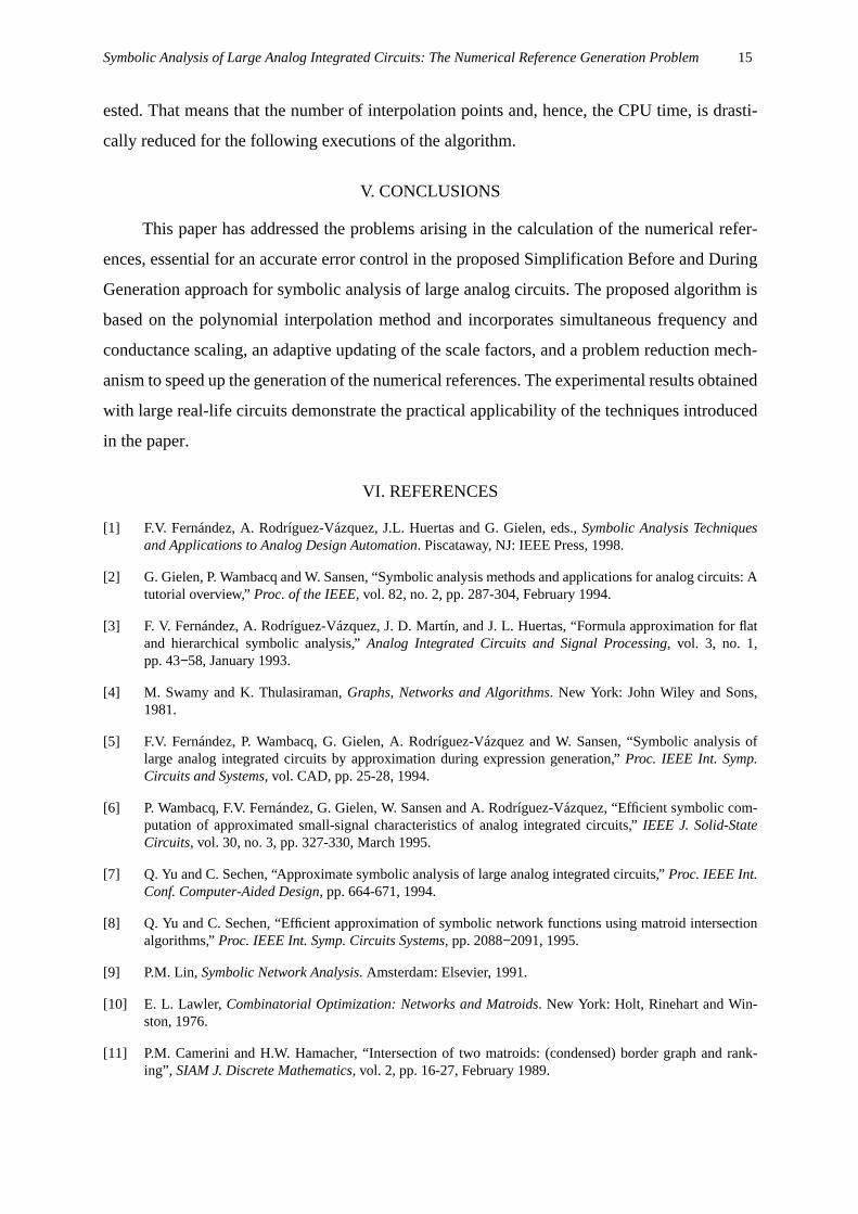
Symbolic Analysis of Large Analog Integrated Circuits: The Numerical Reference Generation Problem15
ested. That means that the number of interpolation points and, hence, the CPU time, is drasti-
cally reduced for the following executions of the algorithm.
V. CONCLUSIONS
This paper has addressed the problems arising in the calculation of the numerical refer-
ences, essential for an accurate error control in the proposed Simplification Before and During
Generation approach for symbolic analysis of large analog circuits. The proposed algorithm is
based on the polynomial interpolation method and incorporates simultaneous frequency and
conductance scaling, an adaptive updating of the scale factors, and a problem reduction mech-
anism to speed up the generation of the numerical references. The experimental results obtained
with large real-life circuits demonstrate the practical applicability of the techniques introduced
in the paper.
VI. REFERENCES
[1] F.V. Fernández, A. Rodríguez-Vázquez, J.L. Huertas and G. Gielen, eds.,Symbolic Analysis Techniquesand Applications to Analog Design Automation. Piscataway, NJ: IEEE Press, 1998.
[2] G. Gielen, P. Wambacq and W. Sansen, “Symbolic analysis methods and applications for analog circuits: Atutorial overview,”Proc. of the IEEE, vol. 82, no. 2, pp. 287-304, February 1994.
[3] F. V. Fernández, A. Rodríguez-Vázquez, J. D. Martín, and J. L. Huertas, “Formula approximation for flatand hierarchical symbolic analysis,” Analog Integrated Circuits and Signal Processing, vol. 3, no. 1,pp. 43−58, January 1993.
[4] M. Swamy and K. Thulasiraman,Graphs, Networks and Algorithms. New York: John Wiley and Sons,1981.
[5] F.V. Fernández, P. Wambacq, G. Gielen, A. Rodríguez-Vázquez and W. Sansen, “Symbolic analysis oflarge analog integrated circuits by approximation during expression generation,”Proc. IEEE Int. Symp.Circuits and Systems, vol. CAD, pp. 25-28, 1994.
[6] P. Wambacq, F.V. Fernández, G. Gielen, W. Sansen and A. Rodríguez-Vázquez, “Efficient symbolic com-putation of approximated small-signal characteristics of analog integrated circuits,”IEEE J. Solid-StateCircuits, vol. 30, no. 3, pp. 327-330, March 1995.
[7] Q. Yu and C. Sechen, “Approximate symbolic analysis of large analog integrated circuits,”Proc. IEEE Int.Conf. Computer-Aided Design, pp. 664-671, 1994.
[8] Q. Yu and C. Sechen, “Efficient approximation of symbolic network functions using matroid intersectionalgorithms,”Proc. IEEE Int. Symp. Circuits Systems, pp. 2088−2091, 1995.
[9] P.M. Lin, Symbolic Network Analysis. Amsterdam: Elsevier, 1991.
[10] E. L. Lawler,Combinatorial Optimization: Networks and Matroids. New York: Holt, Rinehart and Win-ston, 1976.
[11] P.M. Camerini and H.W. Hamacher, “Intersection of two matroids: (condensed) border graph and rank-ing”, SIAM J. Discrete Mathematics, vol. 2, pp. 16-27, February 1989.

Symbolic Analysis of Large Analog Integrated Circuits: The Numerical Reference Generation Problem16
[12] M. Galán, I. García-Vargas, F.V. Fernández and A. Rodríguez-Vázquez, “A new matroid intersection algo-rithm for symbolic large circuit analysis,”Proc. Workshop on Symbolic Methods and Applications to Cir-cuit Design, Leuven, Belgium, 1996.
[13] M. Galán, F.V. Fernández and A. Rodríguez-Vázquez, “Comparison of matroid intersection algorithms forlarge circuit analysis,”Proc. IEEE Int. Symp. Circuits and Systems, pp. 1784-1787, 1997.
[14] R. E. Moore,Methods and Applications of Interval Analysis. Studies in Applied Mathematics, Philadel-phia, 1979.
[15] Jer-Jaw Hsu and C. Sechen, "Fully symbolic analysis of large analog integrated circuits,"Proc. IEEE Cus-tom Integrated Circuits Conf., pp. 21.4.1−21.4.4, 1994.
[16] R. Sommer, E. Hennig, G. Droge, and E.-H. Horneber, “Equation-based symbolic approximation bymatrix reduction with quantitative error prediction,”Alta Frequenza, vol. 5, no. 6, pp. 317−325, November1993.
[17] J. Vlach and K. Singhal,Computer Methods for Circuit Analysis and Design. Van Nostrand Reinhold,1994.
[18] K. Singhal and J. Vlach, “Generation of immittance functions in symbolic form for lumped distributedactive networks,”IEEE Trans. Circuits and Systems, vol. CAS-21, no. 1, pp. 57-67, January 1974.
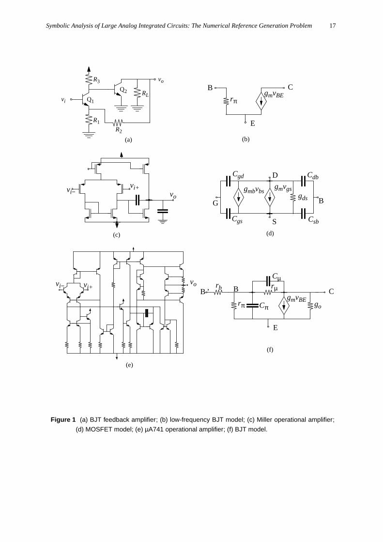
Symbolic Analysis of Large Analog Integrated Circuits: The Numerical Reference Generation Problem17
Figure 1 (a) BJT feedback amplifier; (b) low-frequency BJT model; (c) Miller operational amplifier;
(d) MOSFET model; (e) µA741 operational amplifier; (f) BJT model.
R2
R3
R1
RLvi
vo
Q1
Q2
(a)
vi+vi− vo
vi− vi+
(b)
(c)
voB ’
E
CgmvBErπ goCπ
Cµrb rµB
D
BG
S
gmvgsgmbvbsgds
CsbCgs
Cgd Cdb
(d)
(e)
E
CgmvBErπ
B
(f)

Symbolic Analysis of Large Analog Integrated Circuits: The Numerical Reference Generation Problem18
R2 R4
R1vi
io
C3
G1
G2
sC3
G4
GV & GI
Figure 2 Illustrating an implementation of SBG: (a) Circuit; (b) Formulation of voltage and current
graphs; (c) Simplified graphs.
G1 sC3
G4
GV & GI
SBG
(a)
(b) (c)

Symbolic Analysis of Large Analog Integrated Circuits: The Numerical Reference Generation Problem19
Numerical Reference Generation
Neglect insignificant coefficients
Error evaluation per device
Replace device with smallest contribution
SBG error criterion met?
Formulate two-graphs
Generate next symbolic term
SDG error criterion met?
Figure 3 Symbolic analysis methodology for large analog circuits.
(H(s) for complete circuit)
(H(s) for modified circuit)
Numerical Reference Generation(H(s) for simplified circuit)
Yes
No
YesNoEND
SBG
SDG
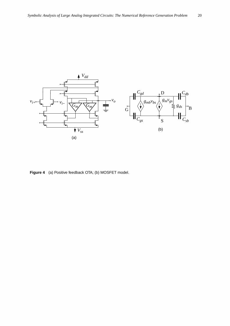
Symbolic Analysis of Large Analog Integrated Circuits: The Numerical Reference Generation Problem20
vi+ vi−
Vdd
Vss
voGm Gm
Figure 4 (a) Positive feedback OTA; (b) MOSFET model.
D
BG
S
gmvgsgmbvbsgds
CsbCgs
Cgd Cdb
(b)
(a)

Symbolic Analysis of Large Analog Integrated Circuits: The Numerical Reference Generation Problem21
Select region of valid coefficients
No
YesEND
Polynomial interpolation
All polynomial coefficients calculated?
Calculate scale factorsfor next interpolation
Problem reduction
Figure 5 Proposed methodology for numerical reference generation for large analog circuits.
CalculateN(sk) andD(sk)
Select initial scale factors

Symbolic Analysis of Large Analog Integrated Circuits: The Numerical Reference Generation Problem22
s0 p0
...
sb pb
sb+1 pb+1
...
sm pm
...
se-1 pe-1
se pe
...
sn pn
Figure 6 Illustrating the adaptive scaling mechanism at the i-th iteration.
pb qb
pm qm
1013 r+×=
gi 1+
gi
q-------=
f i 1+ f i q=
pe qe
pm qm
1013 r+×=
pb
pm--------- 10
13– σ+≥
pe
pm--------- 10
13– σ+≥
region of valid
coefficients
new scale
factors
numerator/denominatorinterpolated coefficients
shift region
to smaller powers
shift regionto higher powers
maximumcoefficient

Symbolic Analysis of Large Analog Integrated Circuits: The Numerical Reference Generation Problem23
1 102 104 106 108
frequency (Hz)
−50
0
50
100
Mag
nitu
de (
dB)
1 102 104 106 108
frequency (Hz)
−800
−600
−400
−200
0
Pha
se (
deg)
Figure 7 Bode diagrams of the voltage gain of the µA741 opamp using the interpolated coefficients
and an electrical simulator.
interpolated coefficients
electrical simulator
interpolated coefficientselectrical simulator

Symbolic Analysis of Large Analog Integrated Circuits: The Numerical Reference Generation Problem24
Figure 8 (a) Bandpass biquad; (b) µA725 opamp.
(a) (b)
vi
vo

Symbolic Analysis of Large Analog Integrated Circuits: The Numerical Reference Generation Problem25
Table 1 Transfer function coefficients for the differential voltage gain of Fig. 4a using interpolationpoints on the unit circle.
si Numerator coefficients Denominator coefficients
s0 −5.8296e−25+j0.0 +8.9418e−30+j0.0
s1 −1.5484e−33−j2.2958e−41 +3.8525e−36−j7.0064e−47
s2 −2.5254e−41+j1.8367e−41 +2.3920e−43−j1.4013e−46
s3 −5.5101e−41+j0.0 +1.0646e−43−j1.4013e−46
s4 +7.3468e−41+j3.6734e−41 −8.4077e−46−j5.6051e−46
s5 −4.5917e−41+j3.5695e−41 +2.1019e−45−j5.4751e−46
s6 +5.5101e−41+j4.1326e−41 −4.2039e−46−j5.6051e−46
s7 +1.8826e−40−j2.0203e−40 +1.0243e−43+j3.0828e−45
s8 −1.1479e−40+j5.5101e−41 −1.8020e−43−j5.6051e−46
s9 −1.7448e−40−j1.6530e−40 +6.8383e−43+j2.5223e−45
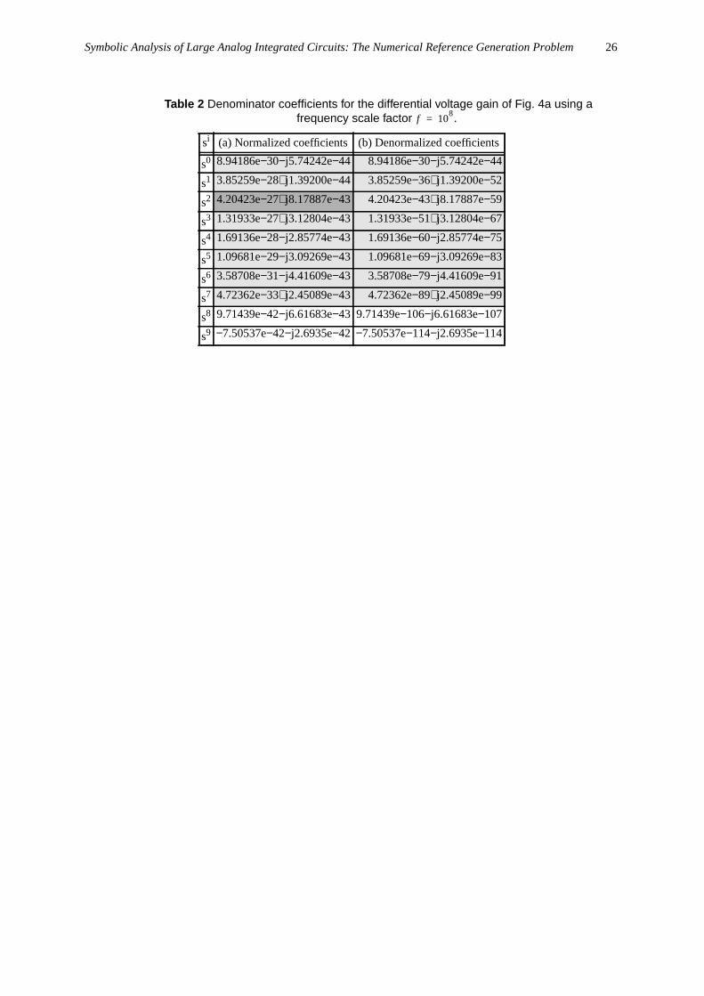
Symbolic Analysis of Large Analog Integrated Circuits: The Numerical Reference Generation Problem26
Table 2 Denominator coefficients for the differential voltage gain of Fig. 4a using afrequency scale factor .
si (a) Normalized coefficients (b) Denormalized coefficients
s0 8.94186e−30−j5.74242e−44 8.94186e−30−j5.74242e−44
s1 3.85259e−28+j1.39200e−44 3.85259e−36+j1.39200e−52
s2 4.20423e−27+j8.17887e−43 4.20423e−43+j8.17887e−59
s3 1.31933e−27+j3.12804e−43 1.31933e−51+j3.12804e−67
s4 1.69136e−28−j2.85774e−43 1.69136e−60−j2.85774e−75
s5 1.09681e−29−j3.09269e−43 1.09681e−69−j3.09269e−83
s6 3.58708e−31−j4.41609e−43 3.58708e−79−j4.41609e−91
s7 4.72362e−33+j2.45089e−43 4.72362e−89+j2.45089e−99
s8 9.71439e−42−j6.61683e−43 9.71439e−106−j6.61683e−107
s9 −7.50537e−42−j2.6935e−42 −7.50537e−114−j2.6935e−114
f 108
=

Symbolic Analysis of Large Analog Integrated Circuits: The Numerical Reference Generation Problem27
Table 3 Valid voltage gain coefficients obtained from the first algorithm iteration on theµA741 opamp in Fig. 1e.
siNumerator coefficients Denominator coefficients
Normalized Denormalized Normalized Denormalized
s0 −9.60926e+122 −5.58675e−86 −2.82408e+118 −1.6419e−90
s1 −1.05987e+124 −2.10393e−91 −7.32222e+122 −1.45352e−92
s2 −1.48757e+124 −1.00824e−97 −8.26327e+123 −5.60064e−98
s3 −1.09256e+124 −2.52835e−104 −1.28095e+124 −2.96432e−104
s4 −4.74222e+123 −3.74701e−111 −1.20867e+124 −9.55018e−111
s5 −1.20465e+123 −3.24992e−118 −7.46903e+123 −2.015e−117
s6 −1.7316e+122 −1.59502e−125 −3.17468e+123 −2.92428e−124
s7 −1.17059e+121 −3.68155e−133 −9.73518e+122 −3.06176e−131
s8 3.98904e+119 4.28355e−141 −2.19449e+122 −2.3565e−138
s9 2.12204e+119 7.7803e−148 −3.61682e+121 −1.32608e−145
s10 3.16408e+118 3.96094e−155 −4.2945e+120 −5.37606e−153
s11 2.81205e+117 1.20194e−162 −3.61821e+119 −1.54651e−160
s12 1.45161e+116 ... −2.13624e+118 −3.11759e−168
s13 3.74942e+114 ... −8.7689e+116 ...
... ... ...
s48 ...

Symbolic Analysis of Large Analog Integrated Circuits: The Numerical Reference Generation Problem28
Table 4 Valid voltage gain coefficients obtained from the second algorithm iteration on theµA741 opamp in Fig. 1e.
siNumerator coefficient Denominator coefficient
Normalized Denormalized Normalized Denormalized
... ... ...
s11 1.26823e+83 1.20194e−162 −1.6318e+85 −1.54651e−160
s12 2.87085e+84 2.11845e−170 −4.22484e+86 −3.11759e−168
s13 3.25114e+85 1.86795e−178 −7.60487e+87 −4.3694e−176
s14 7.09905e+85 3.17579e−187 −9.50869e+88 −4.25375e−184
s15 −2.41332e+87 −8.40596e−195 −8.31808e+89 −2.89732e−192
s16 −3.10937e+88 −8.4327e−203 −5.16263e+90 −1.40012e−200
s17 −1.93746e+89 −4.09119e−211 −2.31064e+91 −4.8792e−209
s18 −7.5856e+89 −1.24718e−219 −7.57228e+91 −1.24499e−217
s19 −2.03572e+90 −2.60601e−228 −1.84185e+92 −2.35783e−226
s20 −3.91629e+90 −3.90351e−237 −3.36737e+92 −3.35638e−235
s21 −5.55819e+90 −4.31356e−246 −4.68533e+92 −3.63616e−244
s22 −5.94529e+90 −3.5925e−255 −5.02443e+92 −3.03607e−253
s23 −4.87733e+90 −2.29471e−264 −4.20538e+92 −1.97857e−262
s24 −3.11448e+90 −1.14091e−273 −2.78054e+92 −1.01858e−271
s25 −1.56748e+90 −4.47086e−283 −1.46833e+92 −4.18806e−281
s26 −6.28204e+89 −1.39512e−292 −6.25244e+91 −1.38854e−290
s27 −2.02144e+89 −3.49537e−302 −2.1642e+91 −3.74221e−300
s28 −5.2559e+88 −7.0762e−312 −6.12909e+90 −8.25182e−310
s29 −1.10938e+88 −1.16293e−321 −1.4274e+90 −1.49631e−319
s30 −1.9069e+87 −1.55641e−331 −2.7438e+89 −2.23949e−329
s31 −2.67406e+86 −1.69938e−341 −4.36393e+88 −2.7733e−339
s32 −3.06103e+85 −1.51463e−351 −5.74996e+87 −2.84515e−349
s33 −2.85887e+84 −1.10143e−361 −6.27718e+86 −2.41839e−359
s34 −2.17505e+83 −5.67206e+85 −1.70147e−369
s35 −1.34446e+82 −4.2331e+84
... ... ...
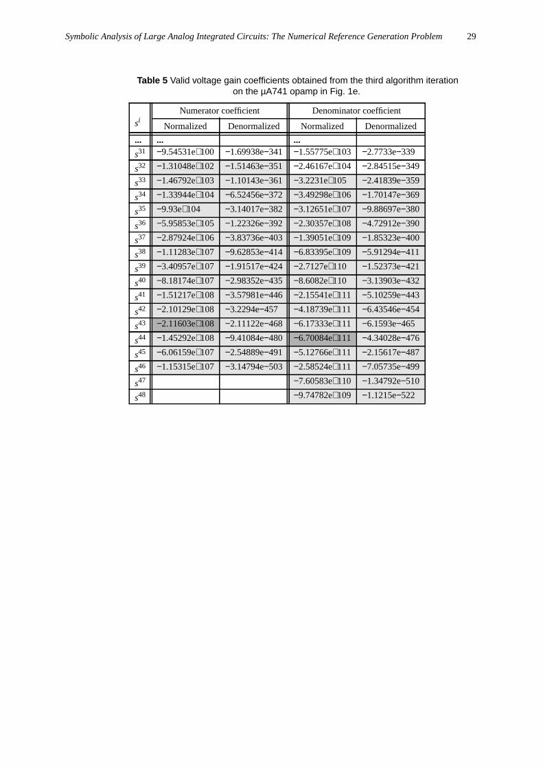
Symbolic Analysis of Large Analog Integrated Circuits: The Numerical Reference Generation Problem29
Table 5 Valid voltage gain coefficients obtained from the third algorithm iterationon the µA741 opamp in Fig. 1e.
siNumerator coefficient Denominator coefficient
Normalized Denormalized Normalized Denormalized
... ... ...
s31 −9.54531e+100 −1.69938e−341 −1.55775e+103 −2.7733e−339
s32 −1.31048e+102 −1.51463e−351 −2.46167e+104 −2.84515e−349
s33 −1.46792e+103 −1.10143e−361 −3.2231e+105 −2.41839e−359
s34 −1.33944e+104 −6.52456e−372 −3.49298e+106 −1.70147e−369
s35 −9.93e+104 −3.14017e−382 −3.12651e+107 −9.88697e−380
s36 −5.95853e+105 −1.22326e−392 −2.30357e+108 −4.72912e−390
s37 −2.87924e+106 −3.83736e−403 −1.39051e+109 −1.85323e−400
s38 −1.11283e+107 −9.62853e−414 −6.83395e+109 −5.91294e−411
s39 −3.40957e+107 −1.91517e−424 −2.7127e+110 −1.52373e−421
s40 −8.18174e+107 −2.98352e−435 −8.6082e+110 −3.13903e−432
s41 −1.51217e+108 −3.57981e−446 −2.15541e+111 −5.10259e−443
s42 −2.10129e+108 −3.2294e−457 −4.18739e+111 −6.43546e−454
s43 −2.11603e+108 −2.11122e−468 −6.17333e+111 −6.1593e−465
s44 −1.45292e+108 −9.41084e−480 −6.70084e+111 −4.34028e−476
s45 −6.06159e+107 −2.54889e−491 −5.12766e+111 −2.15617e−487
s46 −1.15315e+107 −3.14794e−503 −2.58524e+111 −7.05735e−499
s47 −7.60583e+110 −1.34792e−510
s48 −9.74782e+109 −1.1215e−522

Symbolic Analysis of Large Analog Integrated Circuits: The Numerical Reference Generation Problem30
Table 6 Valid denominator coefficients of the voltage gain of the bandpass biquad in Fig. 8aobtained from the (a) first, (b) second, (c) third and (d) fourth algorithm iteration.
si(a) Denominator coefficients
si(b) Denominator coefficients
Normalized Denormalized Normalized Denormalized
... ... s0 −3.91876e+56
s23 −7.51056e+09 s1 −1.01152e+58−4.94769e−230
s24 −5.94246e+10 s2 −7.75231e+59−4.44594e−235
s25 −7.29364e+11−5.2904e−395 ... ... ...
... ... ... s8 −1.04737e+64−1.56051e−272
s40 −5.80151e+18−3.26183e−513 s9 −1.42046e+64−2.48143e−279
s41 −6.87954e+18−1.70385e−521 s10 −1.56628e+64−3.2081e−286
s42 −7.2521e+18 −7.91199e−530 s11 −1.4507e+64 −3.48388e−293
s43 −6.79335e+18−3.2648e−538 s12 −1.163e+64 −3.2747e−300
... ... ... ... ... ...
s58 −1.47487e+12−3.23433e-670 s23 −2.94228e+60−4.76909e−380
s59 −8.03012e+11−1.96111e−679 s24 −8.74623e+59−1.66218e−387
... s25 ...calculated...
si(c) Denominator coefficients
si(d) Denominator coefficients
Normalized Denormalized Normalized Denormalized
s59 ...calculated... s87 ...calculated...
s60 −3.64197e+12−1.05641e−688 s88 ...calculated...
... ... ... s89 −9.84964e+47−3.47589e−978
s68 −1.03089e+15−1.183e−764 ... ... ...
s69 −1.26356e+15−2.2963e−774 s94 −5.04429e+49−3.76528e−1032
s70 −1.39033e+15−4.00138e−784 s95 −7.39434e+49−4.04545e−1043
s71 −1.37471e+15−6.2656e−794 s96 −9.31988e+49−3.73721e−1054
... ... ... s97 −1.00029e+50−2.9399e−1065
s86 −4.32544e+09−1.94841e−946 s98 −9.03506e+49−1.9463ε−1076
s87 −7.99215e+08−5.70129e−957 ... ... ...
s88 −1.41979e+08−1.49098e−967 s104 −3.93227e+47−1.31324e−1145
s89 −1.94284e+07 s105 −4.561e+46 −1.11642e−1157
... ... ... s106 −2.41567e+45−4.33388e−1170

Symbolic Analysis of Large Analog Integrated Circuits: The Numerical Reference Generation Problem31
LIST OF FIGURESFigure 1 (a) BJT feedback amplifier; (b) low-frequency BJT model; (c) Miller operational amplifier; (d)
MOSFET model; (e) mA741 operational amplifier; (f) BJT model.
Figure 2 Illustrating an implementation of SBG: (a) Circuit; (b) Formulation of voltage and current
graphs; (c) Simplified graphs.
Figure 3 Symbolic analysis methodology for large analog circuits.
Figure 4 (a) Positive feedback OTA; (b) MOSFET model.
Figure 5 Proposed methodology for numerical reference generation for large analog circuits.
Figure 6 Illustrating the adaptive scaling mechanism at the i-th iteration.
Figure 7 Bode diagrams of the voltage gain of the µA741 opamp using the interpolated coefficients
and an electrical simulator.
Figure 8 (a) Bandpass biquad; (b) µA725 opamp.

Symbolic Analysis of Large Analog Integrated Circuits: The Numerical Reference Generation Problem32
LIST OF TABLES Table 1 Transfer function coefficients for the differential voltage gain of Fig. 4a using interpolation
points on the unit circle. Table 2 Denominator coefficients for the differential voltage gain of Fig. 4a using a frequency scale
factor. Table 3 Valid voltage gain coefficients obtained from the first algorithm iteration on the µA741 opamp
in Fig. 1e. Table 4 Valid voltage gain coefficients obtained from the second algorithm iteration on the µA741
opamp in Fig. 1e. Table 5 Valid voltage gain coefficients obtained from the third algorithm iteration on the µA741 opamp
in Fig. 1e. Table 6 Valid denominator coefficients of the voltage gain of the bandpass biquad in Fig. 8a obtained
from the (a) first, (b) second, (c) third and (d) fourth algorithm iteration.

Symbolic Analysis of Large Analog Integrated Circuits: The Numerical Reference Generation Problem33
FOOTNOTES
1. The number of terms for Fig. 1c was obtained using ASAP [3] while the lower bound of thenumber of terms for Fig. 1e was calculated using the theory presented in [4].