Embed Size (px)
Citation preview
1404 IEEE J O U R P . ; A I ON SEI.F..(‘TED A R E A S 1’4 COMMUNICATIONS. VOL. X. NO X. O C T O B E R I Y W
Synchronization in Digital System Design
Abstract-In digital system design, synchronization ensures that op- erations occur in the logically correct order, and is a critical hctur in ensuring the correct and reliable system operation. As the physical size of a system increases, or as the speed of operation increases, synchro- nization plays an increasingly dominant role in the system design. Dig- ital communication has developed a number of techniques to deal with synchroniLation on a global and even cosmic scale; and as the clock speeds of chip, hoard, and rwm-sized digital systems increase, they may benefit from similar techniques. Yet, the digital system and digital communication communities have evolved synchronization techniques independently, choosing different techniques and different terminol- ogy. In this paper. we attempt to present a unified framework and terminology for synchronization design in digital systems, borrowing techniques and terminologies from both digital system and digital com- munication design disciplines. We then compare the throughput of syn- chronous and asynchronous interconnect, emphasizing how it is im- pacted by interconnect delay. Finally, we discus5 opportunities to apply principles long employed in digital rommunications to the design of digital systems, with the goal of reducing this dependence on intercon- nect delay.
I . INTRODUCTION
0 PERATIONS in digital systems can either proceed concurrently, or they must obey a precedence rela-
tionship. If two operations obey a preccdcnce, then thc role of synchronization is to ensure that the operations follow in the correct order. Synchronization is thus a crit- ical part of digital system design.
The most common approach to synchronization is to distribute a clock signal to all modules of the system. With the scaling of feature-sizes in VLSI design, clock speeds are increasing rapidly, but increases in complexity tend to prevent significant reductions in chip size. As a con- sequence of this scaling, clock speeds in digital system designs are increasing in relation to propagation delays. This is causing increasing problems with the traditional synchronous design methodologies, certainly at the sys- tem and board levels, and increasingly even wrthin high performance chips [ I ] . This problem will be accentuated with the more common application of optics to system interconnection.
Problems such as large propagation delay have been faced since the earliest days of digital communication sys-
Manuscrlpt recelved JanuaQ IY, IYYO. This work was supported by the National Sciencc Foundation, the California MICRO Program. Rockwell Semiconductor, Level One. and Texas Instruments. This paper was pre- aented at the 6th IEEE International Workshop on Microclectronlcs and Photonics in Communications. New Seabury. Cape Cod, MA, June 6-9, 1989.
The author is wlth the Department ot Electrical Englneerlng and Cou- puter Sciencc. University of California. Berkeley, CA 94720.
IEEE Log Kumber 9036205.
tem design, and hence there are a number of opportunities to apply digital communications principles to VLSI and digital system design. However, because of the wide dif- ference between system physical sizes in relation to clock speeds, the design styles of the communities have devel- oped almost independently. This is in spite of the fact that digital design is a necessary element of digital commu- nication design (for example, in modems, switches, etc.).
In this paper. we place the synchronization problem and design approaches in digital communication and digital system design in a common framework, and then examine opportunities for cross-fertilization between the two fields. In attaining the unification of design methodologies that we attempt in this paper. the first difficulty we face is the inconsistencies. and even contradictions, between terms as used in the two fields. For example, the term “self- timed” generally means “no independent clock,” but as used in digital communication it means no clock at all (in the sense that if a clock is needed it can be derived from the data), and in digital system design it indicates that there is a clock signal that is slaved to the data rather than being independent. Therefore, in Section I1 we attempt to define a taxonomy of terminology that can apply to both fields, while retaining as much of the terminology as pres- ently used as possible. We discuss this terminology in terms of the necessary levels of abstraction in the design process. In Section I11 we discuss the synchronization techniques commonly used in digital systems and digital communications, relate the two, and compare the funda- mental limitations they place on throughput. In Section IV we discuss specifically how some synchronization techniques from digital communication might be benefi- cial in digital system design, particularly in reducing de- pendence of throughput on interconnect delay. Finally, in Section V we discuss briefly the interrelationship between architectural design and synchronization in digital sys- tems. This discussion expands on an earlier conference paper P I ’
11. ABSTRACTIONS I N SYNCHRONIZATION
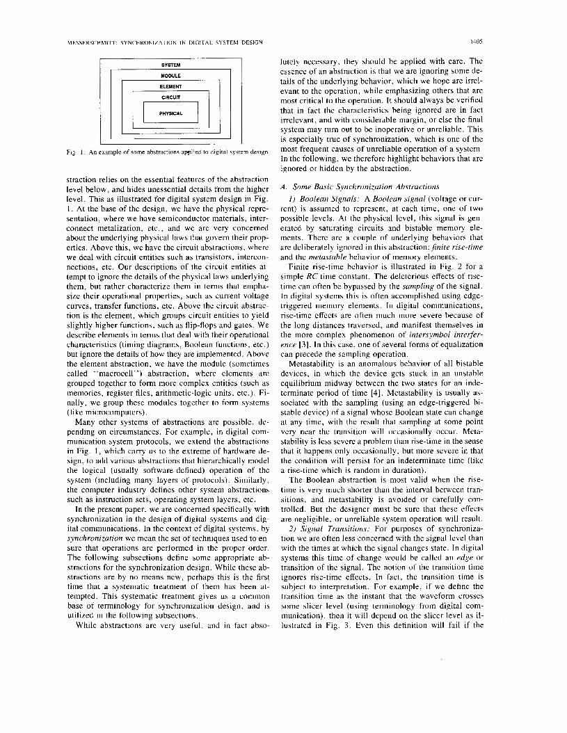
A basic approach in system design is to define absrrac- rions that enable the designer to ignore unnecessary de- tails and focus on the essential features of the design. While every system is ultimately dependent on underlying physical laws, it is clcar that if we relied on the solution of Maxwell’s equations at every phase of the design, sys- tems could never get very complex. Abstractions are often applied in a hierarchical fashion, where each layer of ab-
0733-8716/9011000-1404$01.00 0 1990 IEEE
MESSERSCHMITT. SYNCHRONIZATION I N DIGITAL SYSTEM DESIGN 130s
SYSTEM
MODULE I
~
Fig. I . An example of some abstractions applied to digital system design
straction relies on the essential features of the abstraction level below, and hides unessential details from the higher level. This as illustrated for digital system design in Fig. I . At the base of the design, we have the physical repre- sentation, where we have semiconductor materials, inter- connect metalization, etc., and we are very concerned about the underlying physical laws that govern their prop- erties. Above this, we have the circuit abstractions, where we deal with circuit entities such as transistors, intercon- nections, etc. Our descriptions of the circuit entities at- tempt to ignore the details of the physical laws underlying them, but rather characterize them in terms that empha- size their operational properties, such as current-voltage curves, transfer functions, ctc. Above the circuit abstrac- tion is the element, which groups circuit entities to yield slightly higher functions, such as flip-flops and gates. We describe elements in terms that deal with their operational characteristics (timing diagrams, Boolean functions, etc.) but ignore the details of how they are implemented. Above the element abstraction, we have the module (sometimes called “macrocell”) abstraction, where elements are grouped together to form more complex entitics (such as memories, register files, arithmetic-logic units, etc.). Fi- nally, we group these modules together to form systems (like microcomputers).
Many other systcms of abstractions are possible, de- pending on circumstances. For example, in digital com- munication system protocols, we extend the abstractions in Fig. 1, which carry us to the extreme of hardware de- sign. to add various abstractions that hierarchically model the logical (usually software-defined) operation of the systcm (including many layers of protocols). Similarly, the computer industry dctincs other system abstractions such as instruction sets, operating system layers, etc.
In the present paper, we are concerned specifically with synchronization i n the design of digital systems and dig- ital communications. In the context of digital systems. by synchronization we mean the set of techniques used to en- sure that opcrations arc performed in the proper order. The following subsections define some appropriatc ab- stractions for the synchronization design. While these ab- stractions are by no means new, perhaps this is the first time that a systematic treatment of them has been at- tempted. This systematic treatment gives us a common base of terminology for synchronization design, and i b
utilized in the following subsections. While abstractions are very useful. and in fact abso-
lutely necessary, they should be applied with care. The essence of an abstraction i s that we are ignoring some de- tails of the underlying bchavior. which we hope are irrel- evant to the operation, while emphasizing others that are most critical to the operation. It should always be verified that in fact the characteristics being ignored are in fact irrelevant, and with considerable margin, or else the final system may turn out to be inoperative or unreliable. This is espccially true of synchronization, which is one of the most frequent causes of unreliable operation of a system. In the following, we therefore highlight behaviors that arc ignored or hidden by the abstraction.
A . Some Basic Synchronization Abstractions 1 ) Boolean Signals: A Buolecrn signal (voltage or cur-
rent) is assumed to represent, at cach time, one of two possible levels. At the physical level, this signal is gen- erated by saturating circuits and bistable memory ele- ments. There are a couple of underlying behaviors that are deliberately ignored in this abstraction:$nite rise-time and the metastable behavior of memory elements.
Finite rise-time behavior is illustrated in Fig. 2 for a simple RC time constant. The deleterious effects of rise- time can often be bypassed by the sampling of the signal. In digital systems this is often accomplished using edge- triggered memory elements. In digital communications, rise-time effects are often much more severe because of the long distances traversed, and manifest themselves in the more complex phenomenon of intersymbol interfer- ence [3]. In this case, one of several forms of equalization can precede the sampling operation.
Metastability is an anomalous behavior of all bistable devices, in which the device gets stuck in an unstable equilibrium midway bctwccn the two states for an inde- terminate period of time [4]. Metastability is usually as- sociated with the sampling (using an edge-triggered bi- stable device) of a signal whose Boolean state can change at any time, with the result that sampling at some point very near the transition will occasionally occur. Meta- stability is less sevcrc a problem than rise-time in the sense that it happens only occasionally, but more severe in that the condition will persist for an indeterminate time (like a rise-time which is random in duration).
The Boolean abstraction is most valid when the rise- time is very much shorter than the interval between tran- sitions, and metastability is avoided or carefully con- trolled. But the designer must be sure that these effects are negligible, or unreliable system operation will result. 2) Signal Transitions: For purposes of synchroniza-
tion we are often less concerned with the signal level than with the times at which the signal changes state. In digital systems this time of change would be called an edge or transition of the signal. Thc notion of the transition time ignores rise-time effects. In fact, the transition time is subject to interpretation. For example, if we define the transition time as the instant that the waveform crosses some slicer level (using terminology from digital com- munication). then it will depend on the slicer level as il- lustratcd in Fig. 3. Even this definition will fail if the
oo l loc lo l l l l l l o l l l oo l l~ ioo l l lo ,
Fig. 2. Illustration of a digital slgnal w l t h a hnlte ribe-time a \ generard by an RC time-con\tanr. whers rhs Boolean signal ahsrrac~~uo I > 3 h o w n below
'3 TIME
VOLTAGE
- 1 2 11
Fig. 3 The rranslt ion t m e I, depends o n dicer level 1,.
waveform is not monotonic in the region of the slicer level.
Transition times are a useful abstraction for the case where the rise times are very short in relation to the in- terval between transitions, with the result that the varia- tion in the transition time is negligibly small over the set of all possible definitions of the transition time. Rise-time is governed by underlying physical phenomena, such as transmission line dispersion, and can be reduced by using wider bandwidth drivers or intermediate repeaters. As system clock rates increase, however. for a given inter- connect style the behavior ignored by this abstraction inevitably becomes important.
The transition abstraction can be extended to the notion of unijorm/y spaced transitions. For example, a clock sig- nal can be modeled as a square wave, in which the tran- sitions alternate in sign, and each adjacent pair of transi- tions (called a cycle) rcpresents a time equal to the reciprocal of the clock.frequency. For a data signal, tran- sitions may or may not be present depcnding on the Bool- ean data (see Fig. 2 ) , so we have to introduce the notion of the times where transitions might occur. called a tran- sirion opportunity, whether they actually occur or not. A data signal whose transitions are slaved to a clock with uniformly spaced transitions then has uniformly spaced transition opportunities (an example is shown in Fig. 4). We can think of these transitions as being associated with a clock that has positive transitions at identical times, which we call the ussociated clock. whether or not such a clock signal exists physically.
Uniformly spaced transitions ignore possibie jitter ef- fects in the generation or transmission of the Boolean sig- nals, which often result in small variations in the times between transitions. Hence, there is the nced to define the concepts of instantaneous phase and frequency.
3) Phase and Frequency: For a Boolean signal, we can define a phase and frequency of the signal as the phase and frequency of the associated clock. It is convenient to describe mathematically a clock signal with uniformly spaced transitions as
x([) = p ( ( j + 4) modulo I ) , ( 1 )
where p ( t ) is a 50%' duty cycle pulse
f is the nominalfiequency, and @ is the phase. As 0 varies over the range 0 5 0 < I , the transitions are shifted in time over one cycle. The phase is thus expressed as thc fraction of a cycle. When we have two Boolean signals, the relnrivrpha.re can be cxpressed as the phase difference (4, - I&) bctween their respective associated clocks.
A more general model that includes more possible ef- fects replaces (1) by
whcre f i s the rlorninalfreqcrenc~ of the associated clock. Afis a possible osret i n the nominal frequency, and Q ( r i is the imtanfaneuu.~ phase \ariation versus time. The in- tention here is that @ ( r ) does not embody a frequency offset, but rather any offset from the nominal frequency is summarized by A$ The precise mathematical conditions for this are complicated by thc modulo operation. and also depend on the model for + ( t ) (deterministic signal, ran- dom process, etc.). For example, if + ( t ) is assumed to be a deterministic differentiable and continuous function (with no phase jumps), then it suffices for c # ( r ) to be bounded,
and for such a function the derivative (instantaneous fre- quency) must average to zero,
(where the average is interpreted as a time average). The model of (3) makes the assumption that the average
frequency is a constant, although that average frequency may not be known a priori (for example, when it depends on the free-running frequency of an oscillator). Such a signal is said to be isochronous (from "iso." the Greek root for "equal"\, whereas if the frequency i s not con- stant (Afis actually a function of time), the signal is said to be artisochronous (or "not equal"). An anisochronous signal can be modeled using ( 3 ) . hut the resulting phase will not be bounded. Thus, the essential difference be- tween isochronous and anisochronous signals is the bounded phase condition of (4) .
The time-varying phase in (3) is crucial whcrc we can- not ignore small variations in the intervals betwccn tran-
MESSERSCHMITT SYNCHRONIZATIOU IN DItiI I’AL S V 5 T F M DFSICU I407
sitions, known as pkase jitrer. This jitter is usually ig- nored in digital system design, but becomes quite significant in digital communications, especially where the Boolean signal is passed through a chain of regenerative repeaters [3].
Directly following from the concept of phase is the in- stanraneous,frequenc~, defined as the derivative of the in- stantaneous phase,
lsocnamous ANISOCHRONOUS
TWO BOOLEAN SIGNALS
SYNCHRONOUS - MESOCHRONWS PLESIOCHRONOUS HETEROCHRONOUS
FIR. 5 . A taxonomy of aynchron~zat ion approaches
From ( 5 ) . the instantanPous freyrrency deviation d$ ( f ) / d t has mean value zero, so that C f + A f ) is the averuge frequency.
Given two signals x , ( t ) , i = 1 . 2 with the same nom- inal frequency, and frequency and phase offsets A& and 4, ( t ) , the instantaneous phase difference between the two signals is
= ( A h - A h ) f + (41 ( t ) - @ z ( t ) ) . ( 7 )
4) S V J C ~ R V Z ~ W Z : Having carefully defincd some terms, we can now define some terminology related to the syn- chronization of two signals. A taxonomy of synchroni- zation possibilities is indicated in Fig. 5 [ 5 ] , 131. As pre- viously mentioned, a Boolean signal can be either iso- chronous or anisochronous. Given two data signals, if both are isochronous, the frequency offsets are the samc. and the instantaneous phase difference is 7ero.
Aq5(t) = 0 (8)
then they are said to be synchronous (from the Greek “syn” for “together”). Common examples would be a Boolean signal that is synchronous with its associated clock (by definition), or two signals slaved to the same clock at their point of generation. Any two signals that are not synchronous are asyncl~ronous (or “not to- gether”). Some people would relax the definition of syn- chronous signals to allow a nonzero phase difference that is constant and known.
In practice, we have to deal with several distinct forms of asynchrony. Any signal that is anisochronous will be asynchronous to any other signals. except in thc special and unusual case that two anisochronous signals have identical transitions (this can happen if they are co-gen- erated by the same circuit). Thus, anisochrony is a form of asynchrony .
If two isochronous signals have exactly the same avcr- age frequencyf + A j , then they are called rnesockronous (from the Greek “meso” for “middle”). For mesochro- nous signals. the fact that each of their phases is bounded per (4) ensures also that the phase difference is also bounded,
Aq5(r) 5 24,n,,. (9 ) a fact of considerable practical significance. Two signals generated from the same clock (even different phases of the same clock). but suffering indeterminate Interconnect delays relative to one another, are mesochronous.
Two signals that have average frequencies that are nominally the same, but not exactly the samc (usually be- cause they are derived from the independent oscillators), are plesiochronous (from the Greek “plesio” for “near”). Suppose thc nominal frequencies are bothf, but the actual frequencies are f + Afl and f + A f 2 , then the instantaneous phase difference is
A $ ( [ ) = - A h ) t + ( 4 l ( t ) ~ + z ( t ) ) , (10)
where the first term increases (or decreases) linearly with time. For two plesiochronous signals, it cannot be pre- dicted which has the higher frequency.
Finally, if two signals have nominally diferenr average frequencies. they are called heterochronous (from the Greek “hetcro” for “different”). Usually the toleranccs on frequency are chosen to guarantee that one signal will have an actual frequency guaranteed higher than the other (naturally the one with the higher nominal rate). For ex- ample, if they have nominal frequencies fl and fr. where fi < f r , and thc worst-case frequency offsets are 1 Afl 1 5 q l and I Afi 1 5 q 2 . then we would guarantee this condi- tion iffl and.f2 were chosen such that
fi + rll < f 2 - v 2 . ( 1 1 )
B. Additional Timing Abstractions in Digital Systems
This section has covered some general considerations in the modeling of Boolean signals from a synchroniza- tion perspective. In this subsection we describe a couple of additional abstractions that are sometimes applied i n digital system design, and represent simplifications due to the relatively small physical size of such systems.
I ) Equipotential Region: Returning to Fig. 1. it is often assumed at the level of the element abstraction that the signal is identical at all points along a given wire. The largest region for which this is true is called (by Seitz 161) the equipotential region. Like our other models, this is never strictly valid, but is useful if the actual time it takes t o equalize the potential along a wire is small in relation to other aspects of the signals, such as the associated clock period or rise-time. The equipotential region is a useful concept in digital system design because of the relatively small size of such systems. Howevcr, the element dimen- sions for which it is valid is decreasing becausc of in- creases in clock frequency with scaling, and a single chip
1408 lEhL JOIIRNAI. ON SELECTED AREAS IN COMMUNICATIOUS. VOL. H. NO X. OCTOBER I W O
can generally no longer be considered an equipotential re- gion.
2 ) Ordering of Signals: In the design of digital sys- tems, it is often true that one Boolean signal is s h e d to another, so that at the point of generation the one signal transitions can always be guaranteed to precede the other. Conversely, the correct operation of circuits is often de- pendent on the correct ordering of signal transitions, and quantitative measures such as the minimum time between transitions. One of the main reasons for defining the equi- potential region is that if a given pair of signals obey an ordering condition at one point in a system, then that or- dering will be guaranteed anywhere within the equipoten- tial region.
111. SYNCHRONlZATlON
The role of synchronization is to coordinate the opera- tion of a digital system. In Section 111-A and B, we review two traditional approaches to synchronization in digital system design: synchronous and anisochronous intercon- nection. In Section 111-C, we briefly describe how syn- chronization is accomplished in digital communication systems. This will suggest, as discussed further in Section IV, opportunities to use digital communication techniques in digital system design.
A . Synchronous Interconnection As shown in Fig. 6, each element (or perhaps module)
is provided a clock, as well as one or more signals that were generated with transitions slaved to the clock. The common clock controls the order of operations, ensuring correct and reliable operation of the system.
We will first, in Section 111-A-l), examine some fun- damental limitations in the operation of synchronous in- terconnection, making idealistic assumptions about the ability to control the clock phases in the systcm and ne- glecting interconnect delays. In Section 111-A-2), we will show how pipeline registers can be used to extend the per- formance of synchronous interconnect; and in Section 111-A-3), we will make more realistic estimates of perfor- mance considering the effects of the inevitable variations in clock phase and interconnect delays.
I ) Principle of Synchronous Interconnection: The fun- damental principle of synchronous interconnection is il- lustrated in Fig. 7. In Fig. 7(a) a computarional block C1 is connected to a synchronizing register R1 at its input. This register is clucked using the positive transitions of a periodic clock signal, where the assumption is that the output signal of the register changes synchronously with the positive transition of the clock. The computational block performs the same computation repeatedly on new input signals applied at each clock transition. The purpose of R1 is to control the time at which the computational block starts to perform its work, in order to synchronize it to other computational blocks in the system. This is an edge-triggered logic model, which we employ for its rel- ative simplicity. There is also a more complicated level-
, LEL , ORIGINATING RECEIVING
ELEMENT ELEMENT
Fig. 6 . Synchronous interconnection. in which a common clock is used to synchronize computational elements.
sensitive model that leads to virtually identical conclu- sions.
The performance measures of interest in Fig. 7 are the throughput (rate at which the computation is repeated) and computarional latency (delay from the time a new input is applied until the result is available). Focusing on the latter, inevitably the computational latcncy is not entirely predictable. It is likely that the output signal will change more than once before it finally settles to its final correct value. For example, if the output signal actually consists of M > 1 Boolean signals in parallel, as is often the case. some of those Boolean signals may transition before oth- ers, or some may transition more than once before reach- ing a steady-state value. This behavior is an inevitable consequence of real circuit implementation of the com- putational block, and presents a considerable problem in the synchronization to other computational blocks. As- sume the computational block has a minimum time before any outputs transition, called the propagution time t,,, and a maximum time before all the outputs reach their final and correct values, called the settling time Since set- tling time is the maximum time before the result is guar- anteed to be available, it is also the computational la- tency. It is assumed that the propagation and settling times can be characterized and ensured over expected proccss- ing variations in the circuit fabrication.
The synchronous interconnect isolates the system be- havior from these realities of circuit implementation by setting the clock period T so that there is a certainry pe- riod during which the output signal is guaranteed to be correct? and then samples the output signal again (using another register R2) during this certainty period as shown in Fig. 7(b). Of course, the phase of the clock for R2 must be adjusted to fall i n this certainty period. This intercon- nect is called synchronous because the proper phase of clock to use at R2 must be known in advance-there can- not be any substantial uncertainty or time variation in this phase. With synchronous interconnect. the undesired be- havior (multiple signal transitions and uncertain comple- tion time) is hidden at the output of R2. We can then ab- stract the operation of the computational block, as viewed from the output of R2, as an element that completes its computation precisely at the positive transitions of the second clock, and this makes it easy to synchronize this block with others since the uncertainty period has been eliminated.
MESSEKSCHMITT SYNCHKONIZATION I N DIGIT.4L SYSTEM DESIGN
l o + 1, r Q + 1“ r Q + T + r p r o + T + f , UNCERTAINTY
PERIOD CERTAINTY
PERIOD
(‘2)
Fig. 7 . Synchronmng a computation CI by latching its input. (a) A reg-
A second register R2 at the output samplcs the output signal durlng the lster R I at the input controls the starling time for the computation. (b)
certain(y period. (c) Timing diagram showing the uncertainty and ccr- tainty period (crosshatched) as a lunctlon of the setting time r,, the prop- agation time /,,. and the clock period T.
Given the propagation and settling times, the certainty period is shown as the crosshatched period in Fig. 7(c). The region of time not crosshatched, during which the signal may possibly be changing, is known as the unccr- ruinry period. If two successive clock transitions come at times to and ( to + T ) , the certainty period starts at time ( t o + t r ) , the time when the steady-state output due to the computation starting at time f n is guaranteed, and ends at time ( to + T + f,,), which is the earliest that the output can transition due to the new computation starting at time ( tn + T ) . The length of the certainty period is ( T + ti, - 1 . : ) . An acceptable register clocking phase for R2 requires that this period must be positive in length. or
Alternatively, we can define the rhruughpur of computa- tional block C1 as the reciprocal of the clock period, and note that this throughput is upper-bounded by
The length of the uncertainty period ( r , $ - I,,) is a funda- mental property of the computational block, and the max- imum throughput is the reciprocal of this length. In con- trast, the length of the certainty period depends on the clock period T , and the goal is generally to make this length as small as practical by choosing T small.
The maximum throughput is dependent only on the length of uncertainty period, ( r , 7 - t , , ) , and not directly on the settling time r,,. In Fig. 8, an example 1s given for throughput much higher than thc reciprocal of the settling time (because the uncertainty time is a small fraction of the settling time). In Fig. 8, before each computation is completed, two more computations are initiated. At any
CLOCK PERIOD
__I( SElTUNGTlME
Fig. 8. An example of a synchronous interconnect with a clock period much smaller than the reciprocal of the settling time, due to a small uncertainty period.
point in time, there are three concurrent computations in progress.
The number of concurrent computations is limited only by the inevitable uncertainty in the computational latency. We can give three examples that illustrate a range of pos- sibilities.
Exurnple I : Consider a fiber optic digital communica- tion system, where the “computational block” is not a computation at all but rather a propagation through a guided medium. For this case, due to propagation disper- sion effects, t,, and t,7 are not identical, but close enough that throughputs in the range of 10” bits/s are possible. Assuming a group velocity of 10’ m/s . and a fiber length of 50 km. the settling time is 0.5 ms. At a conservative bit rate of 100 mb/s, there are 50 000 bits propagating through the fiber at any time (“concurrent computations” in the language above). At this velocity and bit rate, the maximum distance for which there is no concurrency in the communication rnediurn is I 111.
Exatnple 2: For typical practical Boolean logic cir- cuits. designed to minimize the settling time rather than maximize the propagation time, /,> is typically very small. and concurrent computations within thc computational block are not possible. Thc maximum throughput is the reciprocal of the settling time. n
E.xample 3: Consider a hypothetical (and perhaps irrl- practical) circuit technology and logic design strategy which is designed to achieve t,, = t , . In this case, thc throughput can be much higher than thc reciprocal of the settling time, and many concurrent computations within the computational block are possible.
While Example 3 is not likely to be achieved, Examples 2 and 3 suggest the possibility of designing circuits and logic to minimize the uncertainty period ( f , ~ f,,) (even at the expense of increasing t , ) rather than minimizing r , as is conventional. For example, one could ensure that every path from input to output had the same number of gates, and carefully match the gate settling times. In such a design style, the throughput could be increased to ex- ceed the reciprocal of the settling timc. This has recently been considered in the literature, and is called w a ~ v pipelining [ 71.
2) Pipelining: The form of concurrency associated with Fig. 8 is known as pipelining. A useful dcfinition of pipelining is the ability to iniriare a new computation at the input to a computational block prior to the cnmnpletion of thc last computation at the output of that block. Since this results in more than a single computation in process within the block at any given time, pipelining is a form of concurrency. always available whcn t,, > 0. The num- ber of pipeline stages is dctined as the number of concur- rent computations in process at one time. For example, if we take the liberty of calling the fiber propagation in Ex- ample 1 a "computation," then the fibcr has 50 000 pipe- line stages.
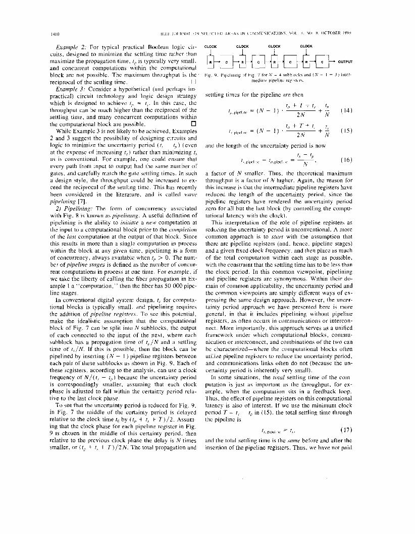
In conventional digital system design, fp for eomputa- tional blocks is typically small, and pipelining requires the addition of pipeline registers. To see this potential. make the idealistic assumption that the computational block of Fig. 7 can be split into N subblocks, the output of each connected to the input of the next, where each subblock has a propagation time of t p / N and a settling time of r T / N . If this is possible, then the block can be pipelined by inserting ( N - 1 ) pipeline registers betwccn each pair of these subblocks a5 shown in Fig. 9. Each of these registers, according to the analysis, can use a clock frequency of N / ( r, - r,) because the uncertainty period is correspondingly smaller, assuming that each clock phase is adjusted to fall within the certainty period rela- tive to the last clock phase.
To see that the uncertainty period is reduced for Fig. 9, in Fig. 7 the middle of thc certainty period is delayed relative to the clock time t(, by (t,> + I , + T ) / 2 . Assum- ing that the clock phase for each pipeline register in Fig. 5, is chosen in the middle of this certainty period, then relative to the previous clock phase the delay is N times smaller, or ( tp + I , + T ) / 2 N . The total propagation and
CLOCK CLOCK CLOCK CLOCK
Fig 9. Plpellninf nf Fig 7 for N = 4 subblocks and ( N ~ I = 3 ) Inter- mediate pipellne reglrrers.
settling timcs for the pipeline are then
and the length of the uncertainty period is now
a factor of N smaller. Thus, the theoretical maximum throughput is a factor of N higher. Again, the reason for this increase is that the intermediatc pipeline registers have reduced the length of the uncertainty period, since the pipclinc registers have rendered the uncertainty period zcro for all but the last block (by controlling the compu- tational latency with the clock).
This interpretation of the role of pipeline registers as reducing the uncertainty pcriod is unconventional. A more common approach is to sfart with the assumption that there are pipeline registers (and, hence, pipeline stages) and a given fixed clock frequency. and then place as much of the total computation within each stage as possible, with the constraint that the settling time has to be less than the clock period. In this common viewpoint, pipelining and pipeline registers are synonymous. Within their do- main of common applicability, the uncertainty period and the common viewpoints are simply different ways of ex- pressing the same design approach. However, the uncer- tainty period approach we have presented here is more general. in that i t includes pipelining without pipeline registers, as often occurs in communications or intercon- nect. More importantly, this approach serves as a unified framework under which computational blocks, commu- nication or interconncct, and combinations of the two can bc characterized-where the computational blocks often utilize pipeline registers to reduce the uncertainty period, and communications links often do not (because the un- certainty period is inherently very small).
In some situations, the rota1 settling time of the com- putation is just as important as the throughput, for cx- ample, when the computation sits in a feedback loop. Thus, the effect of pipeline registers on this computational latency is also of interest. If we use the minimum clock period T = t , - ti, i n (15), the total settling time through the pipeline is
f s , plpellne = f,. (17) and the total settling time is the same before and after the insertion of the pipeline registers. Thus, we have not paid
141 I
a pcnalty i n total settling time in return for the increase i n throughput by a factor of N . since only the variability in settling time has been reduced.
In practice. depending on the system constraints. there are two interpretations of computational latency. as illus- trated in the following cxampleb.
Esclmple 4: In a computer or signal processing system, the pipelinc registers introduce a /ogica/ dclnp, analogous to the 2 -I opcrator in Z-transforms. Expressed in terms of these logical dclays. the N pipeline rcgisters increase computational latency by N (equivalent to a :-” opera- tor). This introduces difficulties. such as unused pipeline stages immediately following a jump instruction. or ad- ditional logical delays in a feedback loop. 0
Erawp/e 5: I n some circumstances, the computational latency ab measured in time is the critical factor. For ex- ample, In the media access controller for a local area nct- work. the time to respond to an external stimulus is crit- ical. For this case. as we have seen, the addition of pipeline registers need not increase the computational la- tcncy at all. With or without pipeline registers, the com- putational latency is bounded below by the inherent pre- cedences in the computation as implemenled by a partic- ular technology. 0
In practice, it is usually not possible to preciscly divide a computational block into “cqual-sized” pieces. In that case, the throughput has to be adjusted to match the larg- est uncertainty pcriod for a block in the pipelme, resulting in a lowered throughput. There are a number of other fac- tors, such as register setup times, which reduce the rhroughput and increase the overall settling time relative to the fundamental hounds that have been discussed here. One of the most important of these is the effect of inter- connect delay and clock skew, which we will address next.
3) Clod SL-PIV i/1 S~~rzc.lz~o~~olcs Ittwrrmwct: The ef- fects of clock phase and itltucm1necr delay (delay of sig- nals passing between computational blocks) wil l now be considered. Clearly. any uncertainty in clock phase will reduce the throughput relative to (13). since earlier results required precise control of clock phase within a vanishing certainty period. Conversely. any fixcd delay in the inter- connect will not necessarily affect the achievable through- put, because it will increase the propagation and settling times equally and thus not affect the length of the uncer- tainty pcriod. In practice, for common dlgital system de- sign approaches, the effect of any unccrtainty in clock phase is magnified by any interconnect delays.
In this subsection, we rclax the previous assumptions, and assume that the clock phase can be controlled only within some known range (similar to the uncertainty pe- riod for the computational block). We then determine the best throughput that can be obtained following an ap- proach similar to [8] and [9].
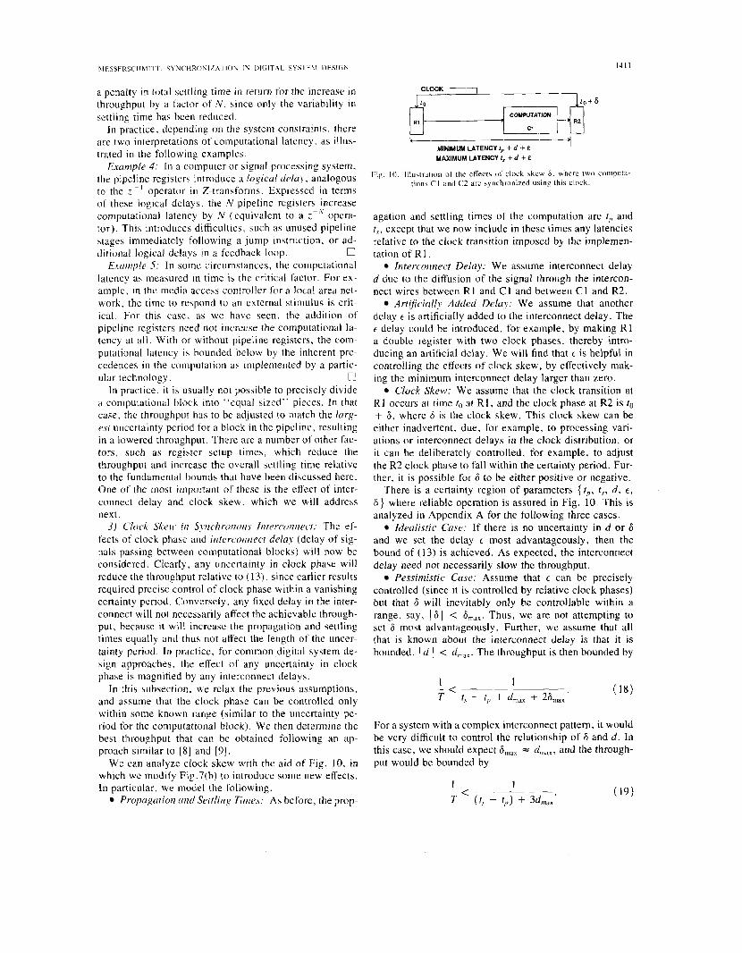
We can analyze clock skew with the aid of Fig. IO . in which wc modify Fig.7(b) to introduce some new effects. In particular, we model the following.
Propagurion c ? n d S r i t l i r ~ ~ Tirnrs: As before, the prop-
agation and settling times of the computation arc r,, and t , , except that we now include in these times any latencies relative to the clock transition imposed by the implemen- tation of R1.
Interconnect Delay: We assume interconnect delay d due to the diffusion of the signal through the intercon- nect wires between R1 and CI and between C1 and R 2 .
ArtiJicially Added Delay: We assume that another delay t is artificially added to the interconnect delay. The t delay could be introduced. for example, by making R1 a double register with two clock phases, thereby intro- ducing an artificial delay. We will find that t is helpful in controlling the effects of clock skew, by effectively mak- ing the minimum interconnect delay larger than zero.
CIock Skevv: We assume that the clock transition at R1 occurs at time to at R1, and the clock phase at R 2 is to + 6. where 6 is the clock skew. This clock skew can be either inadvertent, due, for example, to processing vari- ations or interconnect delays in the clock distribution, or it can be deliberately controlled, for example, to adjust the R2 clock phase to fall within the certainty period. Fur- ther. it is possible for 6 to be either positive or negative.
There is a certainty region of parameters { r,,, t,, d , E ,
6 ) where reliable operation is assured in Fig. 10. This is analyzed i n Appendix A for the following three cases.
Idealisrir Crrse: If there is no uncertainty in d or 6 and we set the delay t most advantageously, then the bound of (13) is achieved. As expected, the interconnect delay need not necessarily slow the throughput.
Pessimistic Case: Assume that E can be precisely controlled (sincc it is controlled by relative clock phases) but that 6 will inevitably only be controllable within a range, say, 16 I < 6,,,. Thus, we are not attempting to set 6 most advantageously. Further, we assume that all that is known about the interconnect delay is that it is bounded, 1 d I < d,,,,,. The throughput is then bounded by
For a system with a complex interconnect pattern. it would be very difficult to control the relationship of 6 and d. In this case, we should expect 6,,, = d,,,,, and the through- put would be bounded by
1412 IEEE JUURNAL ON SELECTED AREAS I N COMMUNICATIOh5. VOL. X. NO. X. OCTOBER IYYO
Optimistic Cuse: For simple topologies like a one- dimensional pipeline, much higher throughput can bc ob- tained by routing the signals and clocks in such a way that d and 6 can be coordinated with one another [8]. Assume that the interconnect delay is known to be do with varia- tion Ad, and the skew is chosen to be 6, with variation As. Further assume that e and 6" are chosen most advan- tageously to maximize the throughput. Then the through- put is bounded by
1 1 - < T ( I , - t,,) + 2 ( A 6 + A d ) '
(20)
which is a considerable improvement over (19) if the de- lay and skew variations are small. This analysis shows that the reliable operation of the idealized synchronous interconnection of Section 111-A-I) can be extended to ac- commodate interconnect delays and clock skew, even with variations of these parameters. albeit with some necessary reduction in throughput.
To get a feeling for the numbers, consider a couple of numerical examples.
Example 6: Consider thc pessimistic case. which would be typical of a digital system with an irregular intercon- nection topology that prevents easy coordination of inter- connect delay and clock skew. For a given clock speed or throughput, we can determine from (19) the largest inter- connect delay d,,,,,, that can be tolerated, namely, ( T - r , ) / 3 , assuming that the interconnect delay and clock skew are not coordinated and assuming the worst-case propagation delay, t,, = 0. For a 100 MHz clock fre- quency, a clock period of 10 ns and, assuming the settling time is 80% of thc clock period, the maximum intercon- nect delay is 667 ps. The delay of a data or clock signal on a printed circuit board is on the order of 5-10 ps/mm (as compared to a free-space speed of light of 3.3 ps/mm). The maximum intcrconnect distance is then 6.7-13.3 cm. Clearly, synchronous interconnect is not vi- able on PC boards at this clock frequency under these pes- simistic assumptions. This also does not take into account the delay in passing through the pins ofa package, roughly 1-3 ns (for ECL or CMOS, respectively) due to capaci- tive and inductive loading effects. Thus, we can see that interconnect delays become a very serious limitation in the board-level interconnection with 100 MHz clocks.
0 Example 7: On a chip, the interconnect delays are much
greater (about 90 ps/mm for AI-Si02-Si interconnect), and are also somewhat variable due to dielectric and ca- pacitive processing variations. Given the same 667 ps in- terconnect delay, the maximum interconnect distance is now about 8 mm. (This is optimistic since it neglects the delay due to source resistance and line capacitance-which will be dominant effects for relatively short intercon- nects.) Thus, we see difficulties in using synchronous in- terconnect on a singlc chip for a complex and global in- tcrconncct topology. 0
Again, it should be emphasized that greater intercon- nect distance is possible if the clock skew and intercon- nect delay can be coordinated. which may be possible if the interconnect topology is simple as in one-dimensional pipeline. This statement applies at both the chip and board levels.
4) Parallel Signal Paths: An important practical im- portance of pipeline registers is in synchronizing the sig- nals on parallel paths. The transition phase offset between these parallel paths tends to increase through computa- tional blocks and interconncct, and can be reduced by a pipeline register to the order of the clock skew across the bits of this multibit register. Again. the register can be viewed as reducing the size of the uncertainty region, in this case spatially as well as temporally.
In Section 111-A-I), we defined the total uncertainty re- gion for a collection of parallel signals as the union of the uncertainty regions for the individual signals. From the preceding, the total throughput is then bounded by the reciprocal of the length of this aggregate uncertainty pe- riod. In contrast, if each signal path from among the par- allel paths wcrc treated independently (say using the mesochronous techniques to be described later), the re- sulting throughput could in principle be increased to the reciprocal of the maximum of the individual uncertainty periods. For many practical cases, we would expect the longcst uncertainty period to include the other uncertainty periods as subsets, in which case these two bounds on throughput would be equal; that is, there is no advantage in treating the signals independently. The exception to this rule would be where the uncertainty periods were largely nonoverlapping due to a relative skew between the paths that is larger than the uncertainty period for each path, in which case there would be considerable advantage to dealing with thc signals independently.
R. Anisochronous Interconnect
The synchronous interconncct approach uses isochro- nous signals throughout the system, since all signals are slaved to an isochronous clock. A popular alternative to synchronous interconnect has been to abandon the iso- chronous assumption, and further abandon the use of a global clock signal altogether. Rather, the elements of the system are chosen to fall within an equipotential region, and the interconnection between elements is designed to operate i n a delay-insensitive manner: that is, opcratc re- liably regardless of what thc delays are. This is accom- plished by having each element of the system generate a cornplerion signal. which has a transition coincident with the settling time of that element. The completion signal is a sort of locally generated clock, and is used to syn- chronize the different elements. Since the completion sig- nal depends on the settling time, which can be data-de- pendent, the resulting signals are anisochronous. For example, if an ALU has two instructions with different settling times, then the signal frequencies will depend on the mix of instructions, and will thus be anisochronous.
MESSERSCHMITT: SYNCHRONIZATION I N DIGITAL SYSTEM DESIGN 1413
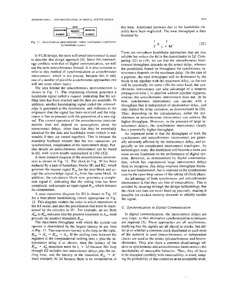
ACKNOWLEDGE
Fig. I I . Anisochronous mterconnectiun. whcrs coord~nation is performed by handshake signals.
In VLSI design. the term self-timed interconnect is used to describe this design approach [6]. Since this terminol- ogy conflicts with that of digital communication, we will use the term anisochronous instead. It is also common to refer to this method of synchronization as asynchronous interconnect, which is not precise, because this is only one of a number of possible asynchronous approaches (we will see some others later).
The idea behind the anisochronous interconnection is shown in Fig. 11. The originating element generates a handshake signal called a rrquest. indicating that the set- tling time has been reached and the data are available. In addition, another handshaking signal called the acknowl- edge is generated at the destination, and indicates to the originator that the signal has been received and the orig- inator is free to proceed with the generation of a new sig- nal. The correct operation of the anisochronous intercon- nection does not depend on assumptions about the interconnect delays, other than that they be essentially identical for the data and handshake wires (which is rea- sonable if they are routed together). This is because the roundtrip feedback ensures that the two operations are synchronized, independent of the interconnect delay. Fur- ther details on anisochronous interconnect can be found in [6], with recent results summarized in [lo]-[12].
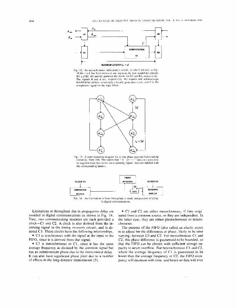
A more detailed diagram of the anisochronous intercon- nect is shown in Fig. 12. The clock in Fig. 10 has been replaced by a pair of handshake blocks HI and H2, which generate the request signal R,,, for the next block and ac- cept the acknowledge signal A,, from that same block. In addition, the calculation block now generates a comple- tion signal C , indicating that the setting time has been completed, and accepts an input signal R,,,, which initiates its computation.
A stutr transition diagrum for HI is shown in Fig. 13 for a four-phase handshaking circuit appropriate in Fig. 12. This diagram models the order in which transitions in the H I occur, and also the precedences that must be main- tained by the circuitry in H1. For example. an arc from A,:, to R:u, indicates that the positive transition in A,,, must precede the positive transition R,,,,.
The maximum throughput with which the system can operate is determined by the largest latency in any loop in Fig. 13. That maximum latency is the loop on the right, R u t + A: + R,, + A , . If the settling time between the registers is the computational settling time t,c plus the in- terconnect delay d as shown, then the latency of the Rot, -+ A; transition must be t.! + 2d because this loop through H2 includes two interconnect delays plus the set- tling time, and the latency in the transition - A,; must similarly be 2d because there is no computation in
this loop. Additional latencies due to the handshake cir- cuitry have been neglccted. The total throughput is thus bounded by
1 1 -5- T t, t 4d '
There are two-phase handshake approaches that are less reliable but reduce the 4d in the denominator to 2d. Com- paring (22) to (19), we see that the anisochronous inter- connect throughput dcpends on the actual delay, whereas the pessimistic bound on throughput for synchronous in- terconnect depends on the maximum delay. (In the case of a pipeline, the total throughput will be dominated by the block in the pipeline with the maximum delay, so the two will be essentially the same.) On the other hand, the syn- chronous interconnect can take advantage of a nonzero propagation time t,, to pipeline without pipeline registers, whereas the anisochronous interconnect does not. At its best, synchronous interconnect can operate with a throughput that is independent of interconnect delay, and only limited by delay variation, as demonstrated in (20). Thus, depending on the circumstances, either the syn- chronous or anisochronous interconnect can achieve the higher throughput, However, in the presence of large in- terconnect delays, the synchronous interconnect clearly has a potentially higher throughput.
An important point is that the throughput of both the synchronous and anisochronous interconnect are gener- ally adversely affected by the interconnect delay, and es- pecially so for complicated interconnect topologies. AS technologies scale, this restriction will bccome a more and more severe limitation on the performance of digital sys- tems. However, as demonstrated by digital communica- tion, which has experienced large interconnect delays from its inception, this delay-imposed throughput limita- tion is not fundamental, but is imposed in the synchronous case by the open-loop nature of the setting of clock phase.
An advantage of both synchronous and anisochronous interconnect is that they arc free of metastability. This is avoided by ensuring through the design methodology that the clock and data are never lined up precisely, making it possiblc for clocked memory elements to reliably sample the signal.
C. Synchronization i n Digital Communication
In digital communication, the interconnect delays are very large, so that alternative synchronization techniques are required [3]. These approaches are all isochronous, implying that the signals are all slaved to clocks, but dif- fer as to whether a common clock distributed to each node of the network is used (mesochronous) or independent clocks are used at the nodes (plesiochronous and hetero- chronous). Thcy also share a common disadvantage rel- ative to synchronous and anisochronous interconnect-thc inevitability of metastable behavior. Thus, they all have to be designed carefully with metastability in mind, keep- ing the probability of that condition at an acceptable level.
I MAXIMUM LATENCY r, + d I
Fig. I ? . An anlsochronous interconnect circuit. in whlch relativc to Fig
H I m d H?. HI and H? generate the clocks tor R I and R 1 . respectively I O the clock ha\ hccn rcmwed and replaced hy twn handshake clrcuits
The signals R and .A arc. respectively, the request and acknowledge
curnpletlon slglial tvr the loglc bloch handshaking signals. esienrially a locally generated clock. and C I \ the
Fig. 13. A state transition diagram tor a four-phase pipelme handahaklng circuit HI from [ I O ] . The superscript "+" or "~ " indicates a positive or negarive Iraniitinn in rhe correiponding clgnal. Arcs are labeled Nith Ihr correapurldirlg latency
CLOCK Cl
1 1 ORIGINATING
MODULE
RECEIVING
MODULE
Fig. 14 An illustration of how thmughput i % made independent of delay in digital communication.
Limitations to throughput due to propagation delay are avoided in digital communications as shown in Fig. 14. First, two communicating modules are each provided a clock-C1 and C2. A clock is also derived from the in- coming signal in the riming recovery circuit, and is de- noted C 3 . These clocks have the following relationships.
C3 is synchronous with the signal at the input to the FIFO, since it is derived from that signal.
C3 is mesochronous to C I . since it has the same average frequency as dictated by the common signal but has an indeterminate phase due to the interconnect delay. It can also have significant phase jitter due to a number of effects in the long-distance transmission [3].
C1 and C2 are either mesochronous, if they origi- nated from a common source. or they are independent. In thc lattcr casc, thcy are either plesiochronous or hetero- chronous.
The purpose of the FIFO (also called an elastic store) is to adjust for the differences in phase, likely to be time varying. between C3 and C2. For mesochronous C1 and C2, this phase difference is guaranteed to be bounded, so that the FIFO can be chosen with sufficient storage ca- pacity to never overflow. For heterochronous CI and C2, where the average frequency of CI is guaranteed to be lower than the average frequency of C2, the FIFO occu- pancy will decrease with time, and hence no data will ever
MESSERSCHMITI' SYNCHROYIZhTION IN DIGITAL SYSTEM DtCIGN
be lost. For plesiochronous CI and C2, the FIFO could overflow, with thc loss of data. if the average frequcncy of C I happens to be higher than C2. This loss of data is acceptable on an occasional basis, but may not be per- missible in a digital system design.
Iv . ISOCHRONOUS Ih.TERC0NNEC.I' IN DIGITAL SYSTEMS
We found previously that the performance of both syn- chronous and anisochronous interconnects in digital sys- tems are limited as a practical matter by the interconnect delays in the system. With the anisochronous approach, this limitation was fundamental to the use of roundtrip handshaking to control synchronization. In the synchro- nous (but not anisochronous) case, we showed that this limitation is not fundamental, but rather comes from the inability to tightly control clock phases at synchronization points in the system. The reason is the "open-loop" na- ture of the clock distribution. making us susceptible to processing variations in delay. If we can more precisely control clock phase using a "closed-loop'' approach. the throughput of the synchronous approach can more nearly approach the fundamental limit of (13), and considerably exceed that of anisochronous interconnect in the presence of significant intcrconnect delays. In this section, we ex- plore some possibilities in that direction, borrowing tech- niques long used in digital communication.
A. Mesochronous Interconnect Consider the case where a signal has passed over an
interconnect and expericnced interconnect delay. The in- terconnect delay does not increase the uncertainty period, and thus does not place a fundamental limitation on throughput. If this signal has a small uncertainty period, as for example it has been resynchronized by a register, then the certainty period is likely to be a significant por- tion of the clock cycle, and the phase with which this sig- nal is resarnpled by another register is not even very crit- ical. Thc key is to avoid a sampling phase within the small uncertainty period, which in synchronous interconnect can be ensured only by reducing the throughput. But if the sampling phase can be controlled in closed-loop fashion, the interconnect delay should not be a factor, as demon- strated in digital communication systems.
Another perspcctive on clock skew is that it results in an indeterminate phase relationship between local clock and signal; in other words, the clock and signal are ac- tually mesochronous. In mesochronous interconnect, we live with this indeterminate phase, rather than attempting to circumvent it by careful control of interconnect delays for clock and signal. This style of interconnect is illus- trated in Fig. 15. Variations on this method were pro- posed some years ago [ 131 and pursued into actual chip realizations by a group at M.I.T. and BBN [14], [15] (al- though they did not use the term "mesochronous" to de- scribe their technique). We have adapted our version of this approach from the mesochronous approach used worldwide in digital communication. except that in this case we can make the simplifying assumption that the
phase variation of any signal or clock arriving at a node can be ignored. The primary cause of the residual phase modulation will be variations in temperature of the wires. and this should occur at very slow rates and at most re- quires infrequcnt phase adjustments. This simplification implies that clocks need not be derived from incoming sign&, as i n the timing recovery of Fig. 14: but rather a distributed clock can be used as a reference with which to sample the received signal. However, we must be pre- pared to adjust the phose of the clock used for sampling the incoming signal to account for indeterminate intercon- nect delays of both clock and signal. We thus arrivc at Fig. IS.
First, we divide the digital system into functional en- tities called "synchronous islands." The granularity of partitioning into synchronous islands is guided by the principle that within an island the interconnect delays are small relative to logic speed, and traditional synchronous design can be used with minimal impact from intercon- nect delays. The maximum size of the synchronous island depends to a large cxtent on the interconnect topology, as we have seen previously. In near-term technology, a syn- chronous island might encompass a single chip within a digital system and, for the longer term, a single chip may be partitioned into two or more synchronous islands. The interconnection of a pair of synchronous islands is shown in Fig. 15(a): externally, the connection is identical to the synchronous interconnection in Fig. 6. The difference is in the relaxed assumptions on interconnect delays.
The mesochronous case requires a more complicated internal interface circuit, as illustrated in Fig. 15(bj . This circuit performs the function of meJochronous-to-s?'n- chronous conversion. similar in function but simpler than the FIFO in Fig. 14. This conversion rcquires the follow- ing.
A clock phase generutor to create a set of discrete phases of the clock. This does not require any circuitry running at speeds greater than the clock speed, but rather can be accomplished using a circuit such as a ring oscil- lator phase-locked to the external clock. A single phase generator can be shared among synchronous islands (such as one per chip), although to reduce the routing overhead it can be duplicated on a per-island or even on a multiple generator per-island basis.
A phase detector determines the certainty period of the signal, for example, by estimating the phase differ- ence between a particular phase of the clock and the tran- sitions of the signal. Generally, one phase detector is re- quired for each signal line or group of signal lines with a common source and destination and similarly routed.
A sampling register R1 with sampling time chosen well within the certainty period of the signal, as con- trolled by the phase detector. This register reduces the uncertainty period of the signal, for example. eliminating any finite rise-time effects due to the dispersion of the in- terconnect, and also controls the phase of the uncertainty period relative to the local clock. Depending on the effect of temperature variations in the system, this appropriate
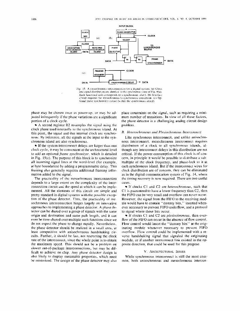
1416 IEEF JOURNAL ON SFLECTED AREAS IN COMMUNICATIONS. V O L X . N O X. OCTOBER IYYO
INPUT CLOCK
1 , , (a) lh , pt CLOCK
PHASE GENERATOR
SELECT
IQ-1 SYNCHRONOUS SYNCHRONOUS g q 1 SYNCHRONOUS ISLAND TO
&
DATA f R A W
SYNCHRONIZER DATA
(c) lREcoLb-< FRAMINQ
DATA PROGRAMMABLE DEIAY DATA
Fig 15. A rncsochronous interconnection for a dlgltal system. (a) Clock and signal diqtrihution are identical to thc synchronous casc of Fig. 6(a). Each functional unit corresponds to a synchronouc island. (h) lnterfacc clrcuil required for nlebochronoua-to-aynchronnua cunvcrslun. (c ) Op- tional frame rynchronizer c~rcuit (wlthin the synchronous island)
phase may be chosen once as power-up, or may be ad- justed infrequently if the phase variations are a significant portion of a clock cycle.
A second register R2 resamples the signal using the clock phase used internally to the synchronous island. At this point, the signal and thls internal clock arc synchro- nous. By inference, all the signals at the input to the syn- chronous island are also synchronous.
If the system interconnect delays are larger than one clock cycle, it may be convenient at the architectural lcvel to add an optional frame synchronizer, which is detailed in Fig. 15(c). The purpose of this block is to synchronize all incoming signal lines at the word-level (for example, at byte boundaries) by adding a programmablc delay. This framing alao generally requires additional framing infor- mation added to the signal.
The practicality of the mesochronous interconnection depends to a large extent vn the complexity of thc inter- connection circuit and the speed at which it can be imple- mented. All the elements of this circuit are simple and pretty standard in digital systems with the possible excep- tion of the phase detector. Thus, the practicality of me- sochronous interconnection hinges largely on innovative approaches to implementing a phase detector. A phase de- tector can be shared over a group of signals with the same origin and destination and same path length, and it can even be time-shared over multiple such functions since we do not expect the phase to change rapidly. Nevertheless, the phase detector should be realized in a small area, at least competitive with anisochronous handshaking cir- cuits. Further, i t should be fast, not restricting the clock rate of the interconnect. sincc the whole point is to obtain the maximum speed. This should not be a problem o n slower out-of-package interconnections, but may be dif- ficult to achieve on-chip. Any phase detector design is also likely to display metastable properties, which must be minimized. The design of the phase detector may also
place constraints on the signal, such as requiring a mini- mum number of transitions. In view of all these factors, the phase detector is a challenging analog circuit design problem.
B. Heterochmnous and Plesiochronous Intercnnncct Like synchronous interconnect, and unlike anisochro-
nous interconnect, mesochronous interconnect requires distribution of a clock to all synchronous islands, al- though any interconnect delays in this distribution are not critical. If the power consumption of this clock is of con- cern, in principle it would be possible to distribute a sub- multiple of the clock frequency, and phase-lock to it at each synchronous island. But if the interconnect wires for clock distribution are of concern, they can be eliminated as in the digital communication system of Fig. 14, where the timing recovery is now required. There are two useful cases.
If clocks C1 and C2 are heterochronous, such that C1 is guaranteed to have a lower frequency than C2, then the FIFO can be very small and overflow can never occur. However, the signal from the FIFO to the receiving mod- ule would have to contain “dummy bits,” inserted when- ever necessary to prevent FIFO underflow, and a protocol to signal where those bits occur.
If clocks C1 and C2 arc plesiochronous, then over- flow of the FIFO can occur in the absence of flow control. Flow control would insert the “dummy bits” at the orig- inating module whenever necesaary to prevent FIFO overflow. Flow control could be implemented with a re- verse handshaking signal that signaled the originating module. or if another interconnect l ink existed in the op- posite direction, that could be used for this purpose.
V . ARCHITECTURAL ISSUES While synchronous interconnect is still the most com-
mon, both anisochronous and mesochronous intercon-
MESSERSCHMITT SYNTHRONIZATION I N DlGlTAL SYSrEM DESIGN 1417
nects are more successful in abstracting the effects of in - terconnect delay and clock skew. Specifically. both design styles ensure reliable operation independent of intercon- nect delay, without the global constraints of sensitivity to clock distribution phase. Each style of interconnect has disadvantages. Mesochronous intcrconnect will have me- tastability problems and requires phase detectors, while anisochronous intcrconnect requires extra handshake wires, handshake circuits, and a significant silicon area for completion-signal generation.
The style of interconnection will substantially influence the associated processor architecturc. The converse is also true-the architecture can be tailored to the interconnect style. As an example, if at the architectural level we can make a significant delay one stage of a pipeline, then the effects of this delay are substantially mitigated. (Con- sider, for example, (22) with f , = 0. )
Many of these issues have been discussed with respect to anisochronous interconnection in [ 161. On the surface one might presume that mesochronous interconnection ar- chitectural issues are similar to synchronous interconncc- tion which. if true, would be a considerable advantage because of the long history and experience with synchron- ous design. However, the indeterminate delay in the in- terconnection (measured in bit intervals at the synchron- ous output of the mesochronous-to-synchronous conversion circuit) must be dealt with at the architectural level. For synchronous interconnection, normally the de- lay between modules is guaranteed to be less than one clock period (that docs not have to be the case as illus- trated in Fig. S), but with mesochronous interconnection the delay can be multiples of a bit period. This has fun- damental implications to the architecture. In particular, i t implies a highcr level of synchronization (usually called “framing“ in digital communications) which line up sig- nal word boundaries at computational and arithmetic units.
In the course of addressing this issue, the following key
information (beginning and end of message, etc.). and de- sign the architecture to use this information. We have studied this problem in some detail in the context of in- terprocessor communication [ 171.
As previously mentioned, each data transfer in an an- isochronous interconnect requires two to four propagation delays (four in the case of the most reliable four-phase handshake). In contrast, the mesochronous interconnec- tion does not have any feedback signals and is thus able to achieve whatever throughput can be achieved by the circuitry, independent of propagation delay. This logic applies to feedforward-only communications. The more interesting case is the command-response situation or. more generally, systems with feedback, since delay will have a considerable impact on the performance of such systems. To some extcnt, the effect of delay is fundamen- tal and independent of interconnect style: the command- response cycle time cannot bc smaller than the roundtrip propagation delay. However, using the “delay build-out” frame synchronizer approach described earlier would have the undesirable effect of unnecessarily increasing the command-response time of many interconnections in the system. Since this issue is an interesting point of contrast between the anisochronous and mesochronous ap- proaches, we w i l l now discuss it in more detail.
A . Commund-Response Processing
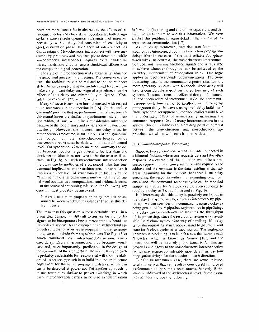
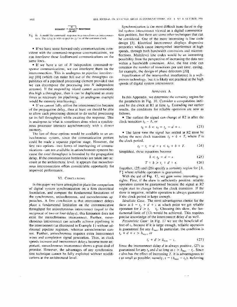
Suppose two synchronous islands are interconnected i n a bilateral fashion, where one requests data and the other responds. An example of this situation would be a pro- cessor requesting data from a memory-the request is the address and the response is the data residing at that ad- dress. Assuming for the moment that there is no delay generating the response within the responding synchron- ous island, the command-response cycle can be modeled simply as a delay by N clock cycles, corresponding to
question must probably be answered: rouihly a delay of 2t,,, as illustrated in Fig. 16.
Is there a maximum propagation delay that can be as- sumed betwccn synchronous islands? If so, is this de- lay modest?
It is intercsting thai this delay is precisely analogous to the delay (measured in clock cycles) introduced by pipe- lining-we can consider this command-response delay as being generated by N pipeline registers. As in pipelining.
The answer to this question is most certainly “yes” in a this delay can be deleterious in reducing the throughput given chip design, but difficult to answer for a chip de- of the processing, since the result of an action is not avail-
- - ~.
signed to be incorporated into a mesochronous board- or larger-level system. As an example of an architectural ap- proach suitable for worst-case propagation delay assump- tions, we can include frame synchronizers like Fig. 15(c) which “build-out” each interconnection to some worst- case delay. Every interconnection thus becomes worst- case and, more importantly, predictable in the design of the remainder of the architecture. However, this approach is probably undesirahle for reasons that will soon he elab- orated. Another approach is to build into the architecture adjustment for the actual propagation delays, which can easily be detected at power-up. Yet another approach is to use techniques similar to packet switching in which cach interconnection carries associated synchronization
able for N clock cycles. One way of handling this delay is for the requesting synchronous island to go into a wait state for N clock cycles after each request. The analogous approach in pipelining is to launch a new data sample each N cycles. which is known as N-slow [Ig]. and the throughput will bc inversely proportional to N. This ap- proach is analogous to the anisochronous interconnection (which may require considerably more delay, such as four propagation delays for the transfer in each direction).
For the mesochronous case, there are some architec- tural alternatives that can result in considerably improved performance under some circumstances, but only if this issue is addressed at the architectural level. Some exam- plcs of these include the following.
REQUEST RESPONSE
Fig. 16. A model for command-response in a mesochrunoua inlcrc(~nnec- t1o11. The delay is wlth re\pect to cyc les of the common clock.
If we have some forward-only communications coin- cident with the command-response communications, we can interleave these feedforward communications on the same lines.
If we have a set of N indcpcndcnt command-re- sponse communications, we can interleave them on the interconnection. This is analogous to pipdirw interleav- ing 1191 (which can make full use of the throughput ca- pabilities of a pipelined proccssing clcmcnt provided that we can decompose the processing into N independent streams). If the responding island cannot accommodate this high a throughput, then it can be duplicated as many times as necessary (in pipelining, an analogous cxamplc would be memory interleaving).
I f we cannot fully utilize the interconnection because of the propagation delay. then at least we should be able to allow each processing element to do uscful proccssing (at its full throughput) while awaiting the response. This is analogous to what is sometimes done when a synchro- nou5 processor interacts asynchronously with a slower memory.
The last of these options would be available to an an- isochronous system, since the communication portion could be made a separate pipeline stage. However, the first two options-two forms of interleaving of commu- nications-are not available in anisochronous systems be- cause the tutu/ throughput is bounded by the propagation delay. If the communication bottlenecks are taken into ac- count at the architectural level, i t appears that mesochro- nous interconnection offers considerable opportunity for improved performance.
VI. CONCLUS~ONS
In this paper we have attempted to place the comparison of digital system synchronization on a firm theoretical foundation, and compare the fundamental limitations of the synchronous, anisochronous, and Inesochronous ap- proaches. A firm conclusion is that interconnect delays place a fundamcntal limitation on the communication throughput for anisochronous interconnect (equal to the reciprocal of two or four delays), this limitation does not exist for mesochronous interconnect. Further, meso- chronous interconnect can actually achieve pipelining in the interconnect (as illustrated in Example 1 ) without ad- ditional pipeline registers, whereas anisochronous can- not. Further, anisochronous requires extra interconnect wires and completion signal generation. Thus, as clock speeds increase and interconnect delays become more im- portant, mesochronous interconnect shows a great deal of promise. However. the advantages of any synchroniza- tion technique cannot be fully exploited without modifi- cations at the architectural level.
Synchronization is the most difficult issue faced in dig- ital system interconnect viewed as a digital communica- tion problem, but there are some other techniques that can be considcrcd. One of the more interesting is line code design [3]. Electrical interconnect displays dispersive properties which cause intersymbol interference at high speeds. through both bandwidth constraints and microre- flections. Multilcvcl line codes would be an interesting possibility from the perspective of increasing the data rate within a bandwidth constraint. Also, the line code can constrain the number of transitions per unit time. easing. for example, the design of phase detectors [20].
Equalization of the intersymbol interference is a wcll- proven technology, but it is likely not practical at the high speeds of digital system interconnect.
A P P ~ U I X A
In this Appendix, we determine the certainty region for the parameters in Fig. I O . Consider a computation initi- ated by the clock at R1 at time to. Extending our earlier results, the conditions for reliable operation are now as follows.
The earliest the signal can change at R2 is after the clock transition to + 6, or
to + 6 < to + t/, + d + t . ( 2 3 ) The latest time the signal has settled at R2 must be
before the next clock transition to + 6 + T , where T is the clock period,
t o + t , + d + t < t o + 6 + T . (24)
Simplified, these equations become 6 < t , + d + t ( 2 5 )
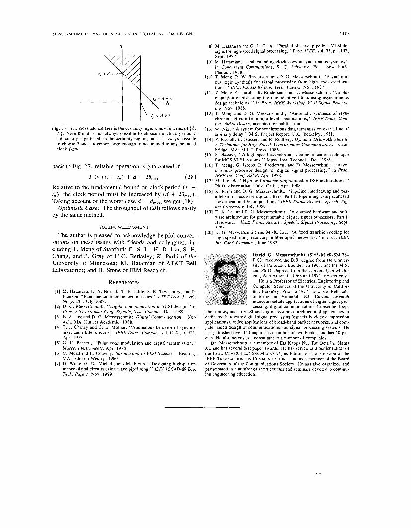
T + 6 > t , + d + t . (26) Together, (25 ) and (26) specify a certainty region for { 6 , T } where reliable operation is guaranteed.
With the aid of Fig. 17. we gain some interesting in- sights. First, if the skew is sufficiently positive, reliablc operation cannot be guaranteed because the signal at R2 might start to change before the clock transition. If the skew is negative, reliable operation is always guaranteed if the clock period is large enough.
Idealistic Case: The most advantageous choice for the skew is 6 = tl, + d + E at which point we get reliable operation for T > f , ~ f,,. Choosing this skew, the fun- damental limit of (13) would be achieved. This requires precise knowledge of the interconnect delay d as well.
Pessimistic Case: In Fig. 17 we see the beneficial ef- fect of E , because if it is large enough, reliable operation is guaranteed for any 6,,,. In particular, the condition is t,, + d + F > or
tp + d > 6,,, - t . (27)
Since the interconnect dclay d is always positive, (27) is guaranteed for any t,, and d so long as E > 6,,,, - t,,. Since F also has the effect of increasing T. it is advantageous to E as small as possible; namely. t = (6 , , , , , - r , j ) . Referring
MESSERSCHMIII SYNCHRONIZATION IN DIGITAL SYSIEM DESIGN
T 1
Flg. 17. The cmsshatched area is the cenainty region, now in terns of { 6, T } . Note that it is not always posslble to choosc rhe clock period T
to choosc T and E together large enough to accommodate any hounded sufficiently large to fall in the ccriainty region, but it 1s always possible
clock skew
back to Fig. 17, reliable operation is guaranteed if
Relative to the fundamental bound on clock period ( r , - t p ) , the clock period must be increased by ( d + 26,,,,,). Taking account of the worst case d = d,,,, we get (18).
Optimistic Case: The throughput of (20) follows easily by the same method.
ACKNOWLEDGMENT The author is pleased to acknowledge helpful conver-
sations on these issues with friends and colleagues, in- cluding T. Meng of Stanford; C . 3 . Li, H.-D. Lin, S.-F. Chang, and P. Gray of U.C. Berkeley; K . Parhi of the University of Minnesota; M. Hatamian of AT&T Bell Laboratories; and H. Stone of IBM Research.
REFERENCES [ I ] M. Hardmian, L . A. Homak, T. E. Little, S. K. Tewkshury, and P.
Franzon, “Fundamental interconnection issues,” AT&T Tech. J., vel. 66, p. 134. July 1987.
[2] D. G . Messerschmitt, “Digital communication in VLSI design,“ In Proc. 23rd Asilomar Conf. Signals, Sysr. Con~put.. Oct. 1989.
131 E. A. Lee and D. G . Messerschmitt, Digital Communicarion. Nor- well, MA: Kluwer Acadcmic, 1988.
[4] T. J. Chaney and C . E. Molnar, “Anomalous behavior of synchro- nizerand arbitercircuits,” IEEE Trans. Compur., vol. C-22. p. 421, Apr. 1973
IS] G. H. Bennett, “Pulse code modulatlon and digital transmis6on,”
161 C. Mead and L. Conway, Introduction ro VLSI Systems. Rcading, Murconi Insrrrtments, Apr. 1978
171 D. Wong. G De Micheli, and M. Flynn. “Designing high-perfor- MA: Addison-Wesley, 1980.
mance digital circuits using wave pipelming,” lEEE ICCAD-X9 Dig. Tech. Papers, Nov. 1989.
1419
[8] M. Hatamlan and G. L Cash, “Parallel bit-level pipelined VLSI de- signs for high-speed signal processing,” Proc. IEEE. k o l . 75, p. 1192, Sept. 1987.
[9] M. Hatamian. “Understanding clock skew in synchronous systems,” in Concurrent Compuralions. S . C . Schwartz, Ed. New York.
[ I O ] T . Meng, R. W. Brodersen, and D. G. Messerschmitt, ”Asynchron- Plenum, 1988.
ous logic aynthesls for signal processing from high-level speclfica- tions,” IEEE ICCAD 87Dig. Tech. Papers, Nov. 1987.
[ I 11 T. Meng, G. Jacobs, R. Brodersen, and D. Messenchmitt. “lmple- mentation of high sampling rate adaptive filten using asynchronous deslgn techniques,” I n Proc. IEEE Workshop VLSI Signal Process- i n g , Nov. 1988.
1121 T. Meng and D. G . Messerschmitt. “Automatic synthesis of asyn-
pur. Aided Design, accepted for publication. chronous circuits from high-level specifications,” IEEE Tram Com-
1131 W. Nix, “A system for synchronous data transmission over a line nf
[I41 P. Bassett, L. Glasser, and R. Rettberg, Dynamic Delay Adjusrmenr: arbitrary delay,” M.S. Project Report, U.C. Berkeley, 1981.
A Technique for Hfgh-Speed Asynchronous Communicarion. Cam- bridge, MA: M.I.T. Press. 1986.
[I51 P. Bassett, “A high-speed asynchronous communication technique for MOS VLSI systems.” Mass. Inst. Technol., Dec. 1985.
1161 T Meng. G. Jacobs, R. Brodersen, and D. Messerschmitt, “Asyn- chronous processor design for digital signal processing,” in Proc.
(171 M. Ilovlch, “Hlgh performance programmable DSP architectures,” IEEE Inr. Conf: ASSP, Apr. 1988.
1181 K. Parhi and D. G . Messerschmitt, “Pipeline interleaving and par- Ph.D. dissertation, Univ. Calif., Apr. 1988.
allelism in recursive digital filters, Part I: Pipelming uslng scattered look-ahcad and decomposition,” IEEE Trans. Acousf , Speech, Si&
[I91 E. A. Lee and D. G. Messerschmitt, “A coupled hardware and soft- nal PrucrJsirrg, July 1989
Hardware,” IEEE Trans. Acouyr., Speech, Signal Processing, Sept. ware architecture for programmable digital signal processors, Part I .
1987. 1201 D. G. Mebserschmitt and M:K. Liu, “A fixed transition coding for
high speed timing recovcry in fiber optics networks,” In Proc. IEEE Inr Con$ Commun.. June 1987.
David G . Messerschmitt (S’6S-M’68-SM’78- F’83) received the B.S. degree from the Univer-
and Ph.D. dcgrees from the University of Mlchl- sity of Colorado, Boulder, in 1967, and the M.S.
gan, Ann Arbor. in 1Y68 and 1971. respcctively.
Computer Sciences at the University of Califor- He is a Professor of Electrical Engineering and
nia. Berkeley. Prior to 1977, he was at Bell Lah- oratories in Holmdel, NJ. Current research interests include applications of digital signal pro-
fiber optics, and m VLSI and digital systems), architectural approaches to cessing, dlgital communications (subscriber loop,
dedlcated-hardware digital signal processing (especially video compression applications), video applications of broad-band packet networks, and com- puter alded design of communications and signal processlng systems. He
ents. He also sewes ab a consultant to a numbcr of companies. has published over 110 papers, is coauthor of two books, and has 10 pat-
Dr. Messerschmitt is a memher of Eta Kappa Nu, Tau Beta PI, Sigma Xi, and has several best paper awards. He has served as a Senior Editor of the IEEE CohlMUNlCATlONs MAGAZINE, as Editor for Transmission of the
of Governors of the Communications Society. He has also organized and partnpated I n a number of short courses and seminars devoted to continu- ing engineering education.
IEEE TRANSACTIONS ON COMMIINICATIOhS, and as a memher of the Board


![Operating Systems Engineering Locking & Synchronization [chapter #4]](https://img.pdfslide.net/doc/110x75/568162ba550346895dd34475/operating-systems-engineering-locking-synchronization-chapter-4.jpg)