Embed Size (px)
Citation preview
Comparative study of the properties of ZnO layers grown by MBE and RF sputtering techniques
BY
MUHAMMAD FAISAL MALIK
DEPPARTMENT OF PHYSICS
The Islamia University of Bahawalpur
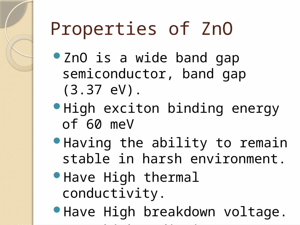
Properties of ZnOZnO is a wide band gap
semiconductor, band gap (3.37 eV).
High exciton binding energy of 60 meV
Having the ability to remain stable in harsh environment.
Have High thermal conductivity.Have High breakdown voltage. Have high radiation tolerance
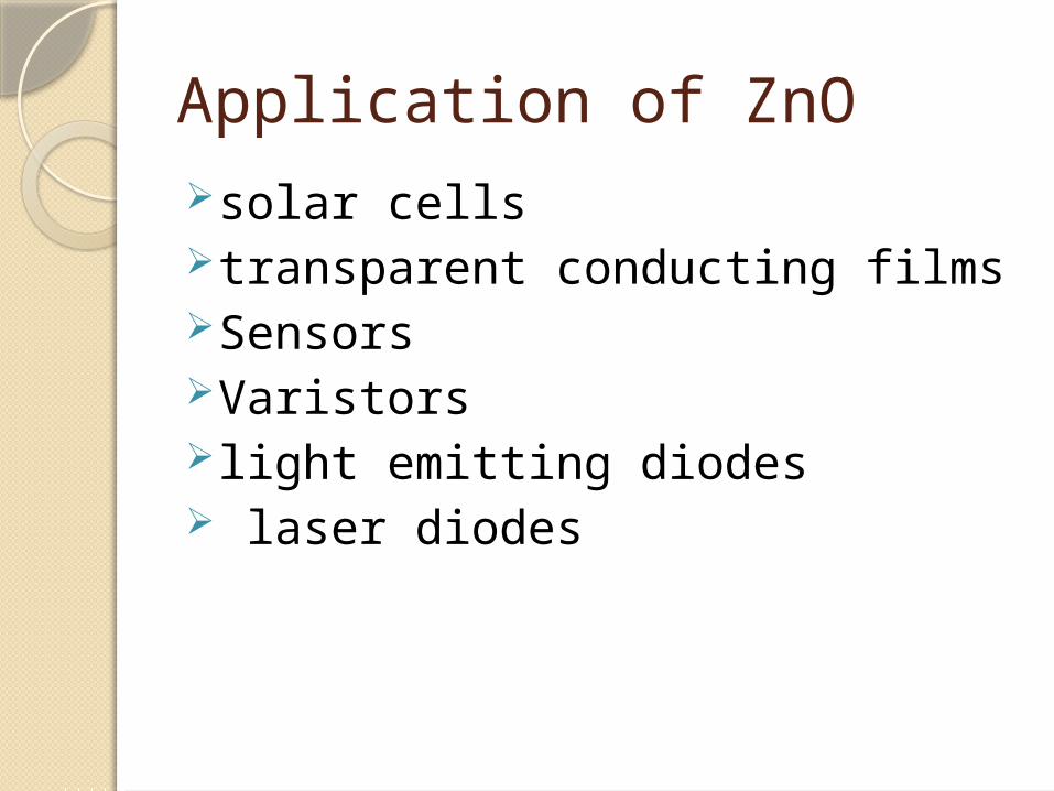
Application of ZnOsolar cells transparent conducting filmsSensorsVaristorslight emitting diodes laser diodes
Deposition Techniques The growth technique played a significant role in
controlling the properties of ZnO films, because the same material deposited by two different techniques, usually had different physical properties. This was due to the fact that the electrical and optical properties of the films strongly depended on the structure, morphology and nature of impurities present. Moreover the films grown using any particular technique might have different properties due to the variation of the deposition parameters and hence the properties can be tailored by controlling the deposition parameters. It was, therefore, important and necessary to make a detailed investigation on the different techniques used for the deposition of ZnO films.
Molecular beam epitaxy Molecular beam epitaxy (MBE) is a method of growing epitaxial
films first pioneered in the 1970’s[20]. Growth is carried out in an ultra high vacuum environment, which minimises the potential for contamination of films. Growth occurs when diffuse molecules or atoms from a material source (effusion cell) are directed at a substrate,
MBE is capable of layer-by-layer growth with excellent control of the purity and crystalline quality of the resulting film. The main advantage of molecular-beam epitaxy (MBE) is its precise control over the deposition parameters. With the feedback from reflection high-energy electron diffraction (RHEED), the growth mode of ZnO epilayer can be monitored in real time dynamically. For ZnO thin-film deposition by MBE, Zn metal and O2 are usually used as the source materials. MBE grown ZnO films can vary considerably in surface morphology, displaying columnar growth, hexagonal island formation, “brain” like structures.

RF sputtering Sputtering is a technology in which the
material is released from the source at much lower temperature than evaporation. The substrate is placed in a vacuum chamber with the source material, named a target, and an inert gas (such as argon) is introduced at low pressure. A gas plasma is struck using an RF power source, causing the gas to become ionized. The ions are accelerated towards the surface of the target, causing atoms of the source material to break off from the target in vapour form and condense on all surfaces including the substrate.
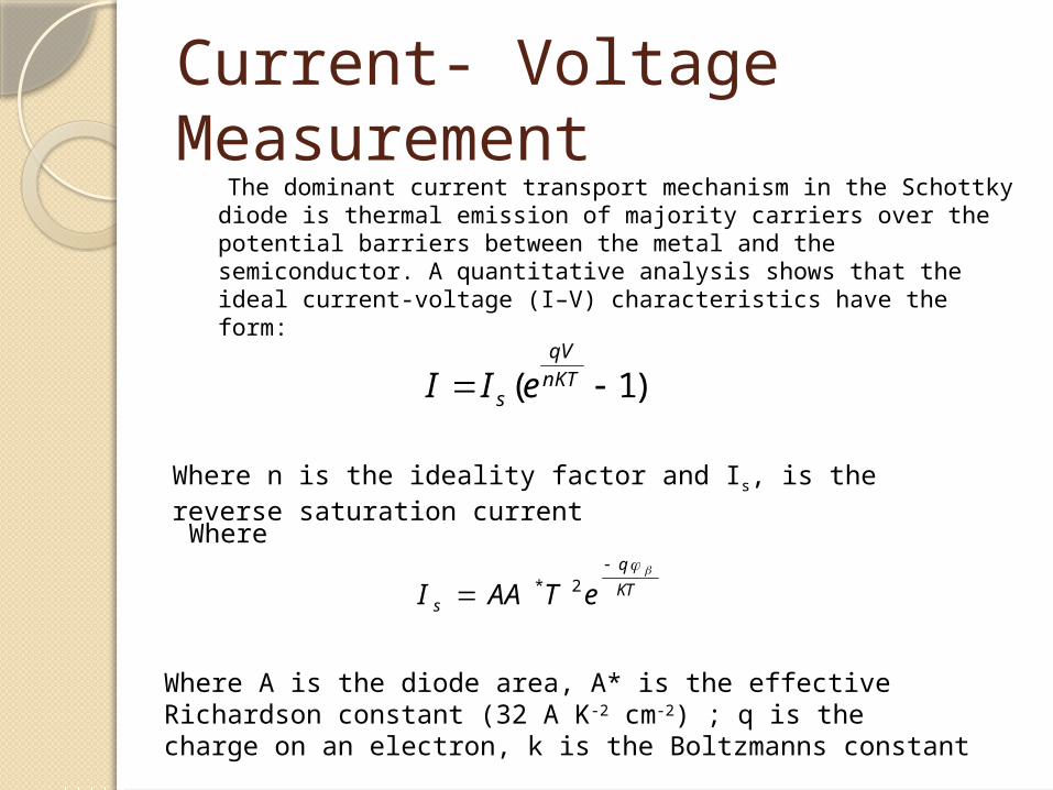
Current- Voltage Measurement The dominant current transport mechanism in the Schottky diode is
thermal emission of majority carriers over the potential barriers between the metal and the semiconductor. A quantitative analysis shows that the ideal current-voltage (I–V) characteristics have the form:
)1( nKT
qV
s eII
Where n is the ideality factor and Is, is the reverse saturation currentWhere
KT
q
s eTAAI
2*
Where A is the diode area, A* is the effective Richardson constant (32 A K-2 cm-2) ; q is the charge on an electron, k is the Boltzmanns constant
Deep Level Transient Spectroscopy
DLTS measurements have been widely used in the study of deep levels in materials and devices. The tool has been used to assign ‘thermal signatures’ to certain deep levels, characterized by an activation energy and its corresponding capture cross-sectional area. It is also used in comparing how these ‘thermal signatures’ vary when processing or growth conditions change.
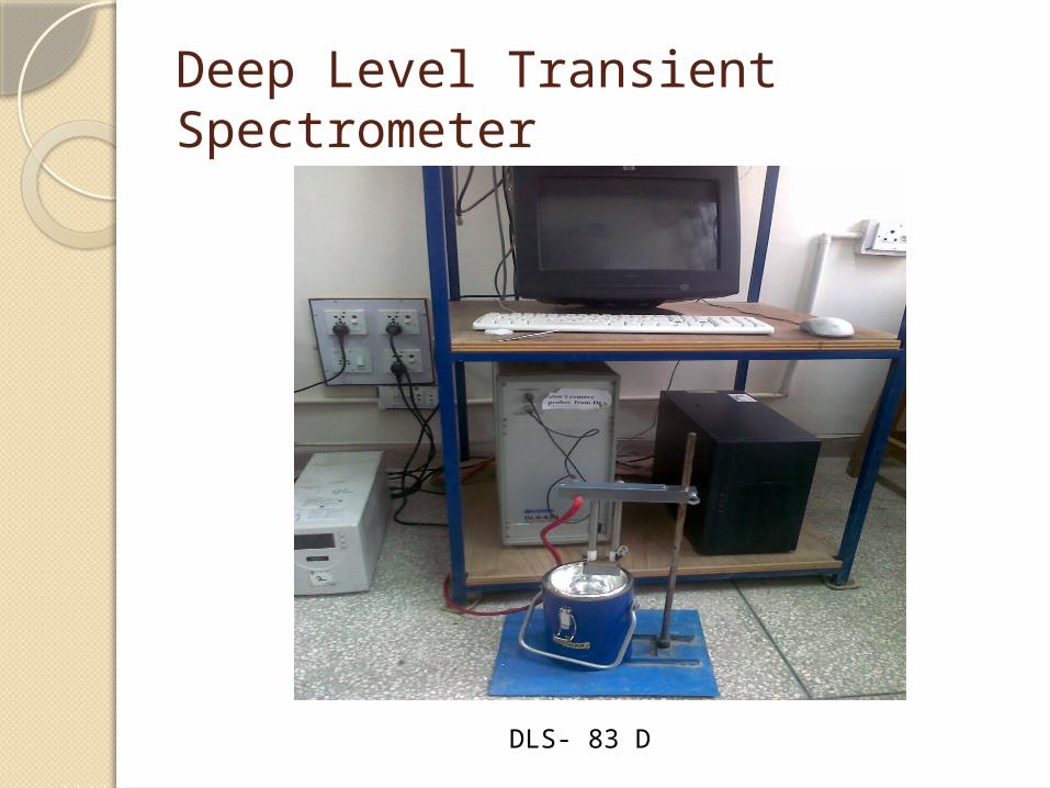
Deep Level Transient Spectrometer
DLS- 83 D

DLTS: principle of operationDLTS uses capacitance transient signals resulting from relaxation
processes following an abrupt change of bias voltage or light applied to the sample being investigated.
Summary about DLTS A standard protocol, described below
briefly, was adopted for DLTS measurements: Acquiring/preparation of samples: Sb-Ge
samples were acquired with essential details about samples.
Fabrication and I-V characterization of Schottky contacts to ensure its good I-V characteristics or low leakage current.
C-V characterization of Schottky barriers to study voltage dependence capacitance response of diodes.
DLTS scans for analysis of samples.
Photoluminescence Spectroscopy In this experiment, the energy levels in
a semiconductor quantum well structure are investigated using the technique of photoluminescence (PL). A laser is used to photoexcite electrons in a semiconductor and when they spontaneously de-excite they emit luminescence. The luminescence is analyzed with a spectrometer and the peaks in the spectra represent a direct measure of the energy levelsin the semiconductor
Facilities
In semiconductor lab (IUB) the following characterization techniques are available
Burker Tensor 27 (for Fourier transform infrared spectroscopy)
Hitachi Model S-3000H (Scanning electron microscopy) Keithley 6487 Picoammeter/voltage source (for current-
voltage) 7200 Boonton capacitance meter ( for capacitance- voltage
measurement) DLS-83D deep level spectrometer, Hungary (for deep level
transient spectroscopy) 4285A LCR meter ( 75kHz- 30MHz) (for capacitance voltage
measurement at different levels and frequencies) Thermal evaporation coating unit Raman and PL
Collaboration In semiconductor lab (IUB), the facilities of any growth technique
and optical measurements are not available due to lack of funds. In order to overcxome the problem the semiconductor lab is collaborated with other universities.
The collaborators are listed below Prof. Dr. M. Willander (ITN, Linköping University, Campus
Norrköping, Norrköping Sweden) Prtof. Dr. Q. Wahab (IFM, Linköping University, Linköping
Sweden) Prof. Dr.M-A Hassan (Department of Electrical and computer
Engineering and the Center for optoelectronic and optical communication, University of North Carolina Charlotte, USA)
Prof. Dr. Shehzad Naseem (MERC, University of the Punjab, Lahore Pakistan)
Dr. A. Mahmood (National Institute of Optoelectronics of Pakistan, Islamabad, Pakistan)
Dr. A. S. Bhatti (Department of Physics, COMSAT Institute of Technology, Islamabad, Pakistan)

Present Study In this study we will grow the ZnO
wafers by MBE and RF sputtering technique and then we will characterize it optically (SEM, XRD, and PL) and electrically (I-V, C-V, and DLTS). These characterization techniques will give us the structural study as well as electrical and optical characterization. This will help us to characterize growth related defects in ZnO. After this study we will be able to achieve the following goals and objectives.

Expected Goals and ObjectiveTo realize the potential of high performance ZnO
based optical and electronic devices. It will help in understanding the deep levels in
ZnO, so the long life and high performance devices can be achieved
Correlation between the main technological parameters and material properties.
By the reduction in cost of ZnO based devices, eventually industry and common man will get benefit from these devices.
The better understanding of characterization of defects in ZnO helps to increase the efficiency of solar cells, transparent electrodes and blue/UV light emitting devices.