Embed Size (px)
Citation preview

GUOHUA LIU
Synthesis and Applications of Free-standing TiO2 Nanotube Membranes
Thesis submitted for the degree of
Philosophiae Doctor
Department of Micro and Nano Systems Technology
Faculty of Technology and Maritime Sciences
Vestfold University College
2013

© Guohua Liu, 2013
Synthesis and Applications of Free-standing TiO2 Nanotube Membranes
ISBN: 978-82-7860-233-1 (print) / ISBN: 978-82-7860-234-8 (online)
Doctoral theses at Vestfold University College, no. 2
ISSN: 1893-7500 (print) / ISSN: 1893-9007 (online)
All rights reserved. No part of this publication may be reproduced or transmitted, in any
form or by any means, without permission.
Cover: Metro Branding
Printed at LOS digital
G. Liu: Synthesis and Applications of Free-standing TiO2 Nanotube Membranes
i
Declaration
I certify that except where due acknowledgement has been made, the work is that of the
author alone; the work has not been submitted previously, in whole or in part to qualify
for any other academic award; the content of the thesis is the result of work which has
been carried out since the official commencement date of the approved research
program; any editorial work, paid or unpaid, carried out by a third party is
acknowledged; and, ethics procedures and guidelines have been followed.
Guohua Liu, Horten
January 28, 2013

G. Liu: Synthesis and Applications of Free-standing TiO2 Nanotube Membranes
iii
Abstract
Nanostructured TiO2 nanotubes (TNTs) have great application potential in
optoelectronic devices due to large effective light harvesting surface area and wide band
gap. Anodization of Ti is a simple way to prepare well-ordered nanostructured TiO2 in
the form of vertically oriented TNTs. Compared with dense nanoparticles, TNTs
facilitate charge transport along the tube direction while maintaining a high effective
surface area, and thus suitable for a variety of applications such as sensors, water
splitting, photovoltaic devices, CO2 conversion, supercapacitors etc.
In order to form a well-ordered tubular structure with controlled morphology, a balance
between oxidation and field-assisted dissolution has to be maintained by adjusting
electrolyte concentration, temperature, anodic duration, ramp rate and the applied
potential. However, the nature of TNTs attached to an opaque Ti foil and with a closed
bottom limits their feasibility for use in extensive applications. Therefore, built upon
suitable fabrication approaches that enable free-standing TNT membranes as well as the
investigation of their photoconductive properties so that create environmental friendly
alternative energy sources are the motivations of this work.
This Ph.D. work focuses on the challenging issues: i) improve the tune quality of highly
ordered TNTs by reproducible manner. ii) Investigate pioneered technologies to prepare
the free-standing TNT membrane as well as mechanism behind the detachment process.
iii) Explore the photoconductive property of the TNTs. Following progresses have been
made towards the target.
Article I provided an overview of all technologies to prepare free-standing TNT
membranes. The developments of structural optimization techniques of the detached
membrane are described from electrochemistry point of view. The application status for
solar cells, water splitting, hydrogen sensors, supercapacitors, CO2 reduction and
photocatalysis are highlighted.
Article II developed a simple process to fabricate flat and mechanically robust free-
standing amorphous TNT membranes. Rinsing the as-prepared TNT membranes by pure
ethanol and reducing the rate of ethanol evaporation are key steps to prepare a large
scale, flat surface membranes. Article III performed a voltage-dependent investigation
for the detachment process of free-standing crystalline TNT membrane. The membrane

G. Liu: Synthesis and Applications of Free-standing TiO2 Nanotube Membranes
iv
detached at low voltage preserves its nanotube morphology and the bottom of tubes are
closed, while through-hole membrane with fast detachment can be observed at a high
detachment voltage.
Article IV reported controllable fabrication of free-standing crystallized TNT
membranes and study their photoconductive properties by optoelectronic technique. The
membrane exhibits a sensitive spectral response to the UV light. These photoresponse
origins from internal gain induced by desorption of oxygen molecules from the
nanotube surfaces and reduction of the barrier at neighboring tubes under UV
illumination.
Article V compared the UV light sensitivity between the small diameter nanotubes ~
20nm and the conventional 140nm diameter TNTs. The small diameter nanotube device
enhances the UV photoresponsivity and leads to a larger increase of photocurrent. We
attribute this improvement to the modulation of hole carrier density as a result of field
effects from the diameter-dependent population of the surface-trapped electrons.
Article VI investigated the effects of applied potential, anodized duration and post-
treatment on the growth and morphology of the anodic TNTs. Article VII carried out a
series of electrochemical anodization experiments to understand the formation
mechanism and to increase control over the morphology of free-standing TNT
membranes.
Article VIII aims to review current knowledge of photocatalytic conversion of CO2
towards solar fuels over TiO2. The basic principle of photocatalytic synthesis is
described, and then engineering design of the TiO2 photocatalysts are emphasized with
respect to reaction parameters. The links between photocatalytic properties of
nanostructured TiO2 and CO2 conversion by using solar energy are addressed. In
addition, rationally orienting the nanostructured TiO2 in chemical reactors for the CO2
conversion and prospects are highlighted for further development.
Key words: Anodization, TiO2 nanotubes, Free-standing membranes, Photoconductivity,
Solar fuels.

G. Liu: Synthesis and Applications of Free-standing TiO2 Nanotube Membranes
v
Preface
This thesis is submitted in candidacy for the Ph.D. degree from Vestfold University
College (VUC), Norway. It is based on the work carried out at Department of Micro and
Nano Systems Technology, VUC-IMST from January 2010 to December 2012.
Financial support was provided by the KD program (08665) at the VUC, Oslofjord
Fund and NorFab consortium in Norway.
I would like to thank my first supervisor Professor Kaiying Wang for his guidance,
encouragement and support during my PhD candidature. I am especially grateful for his
tireless assistance on my experiments and papers. Special thanks to my second
supervisor associate Professor Nils Hoivik, for his enlightening ideas and discussions to
my work. Many thanks to master student Wenran Gu, Waqas Ahmad, Qiong Chen and
Ying Zhao for their continuing friendship.
I am also grateful to the VUC staffs, IMST laboratory members as well as my research
friends. Appreciations go to the following people for their technical assistance and
guidance: Prof. Einar Halvorsen and Knut Aasmundtveit for their invaluable input of
knowledge; Zekija Ramic and Ragnar Dohansen for help of the experimental set up;
Tormod Vinsand for help with SEM; Vishnukanthan Venkatachalapathy for help of
XRD; Xiaoming Wang for help of TEM.
Last but not least, my deepest appreciation and sincere gratitude are extended to my
parents and relatives for their unconditional love, understanding and support accompany
along my PhD journey. None of this would be possible without their love and concerns.
Guohua Liu, Horten
January 28, 2013


G. Liu: Synthesis and Applications of Free-standing TiO2 Nanotube Membranes
vii
List of articles
The thesis is based on the following five papers:
I. Guohua Liu, Kaiying Wang, Nils Hoivik and Henrik Jakobsen, Progress on free-standing and flow-through TiO2 nanotube membranes, Solar Energy Materials and Solar Cells, 98 (2012) 24-38. (Top 25 Hottest Articles in 2012 full year) Contribution: Material collection, Draft writing
II. Guohua Liu, Kaiying Wang, Nils Hoivik and Henrik Jakobsen, Reducing solvent evaporation rates for the detachment of anodic TiO2 nanotubular membranes, MRS Online Proceedings Library, 2012, Volume 1442. Contribution: Experiment, Manuscript preparation
III. Guohua Liu, Nils Hoivik, Kaiying Wang and Henrik Jakobsen, A voltage-dependent investigation on detachment process for free-standing crystalline TiO2 nanotube Membranes, Journal of Materials Science, 46(2011)7931-7935. Contribution: Experiment, Data analysis and interpretation
IV. Guohua Liu, Nils Hoivik, Xiaoming Wang, Shushen Lu, Kaiying Wang and Henrik Jakobsen, Photoconductive, free-standing crystallized TiO2 nanotube membranes, Electrochimica Acta, 93 (2013) 80-86. Contribution: Conception, Experiment, Data analysis
V. Guohua Liu, Nils Hoivik and Kaiying Wang, Small diameter TiO2 nanotubes with enhanced photoresponsivity, Electrochemistry Communications, 28 (2013) 107-110. Contribution: Conception, Experiment
Additional contributions:
VI. Guohua Liu, Kaiying Wang, Nils Hoivik and Henrik Jakobsen, Growth and morphology of highly ordered TiO2 nanotube arrays via electrochemical anodization, ECS Transactions, 41 (2012) 19-27. Contribution: Experiment, Data analysis
VII. Guohua Liu, Nils Hoivik, Kaiying Wang and Henrik Jakobsen, Free-standing TiO2 nanotube membranes from electrochemical anodization, IEEE, NANO No.127 (2011) 1011-1015, August 15-19, Portland, Oregon, USA. Contribution: Experiment, Draft writing
VIII. Guohua Liu, Nils Hoivik, Kaiying Wang and Henrik Jakobsen, Engineering TiO2 nanomaterials for CO2 conversion/solar fuels, Solar Energy Materials and Solar Cells, 105 (2012) 53-68. (Top 25 Hottest Articles from July to December 2012) Contribution: Material collection, Draft writing
Publications not enclosed in the thesis:
IX. Waqas Ahmad, Guohua Liu, Nils Hoivik, Kaiying Wang, Ultraviolet Photodetector Translated from Crystalline TiO2 Nanotube Arrays, Proceedings of the 3rd International Conference on Nanotechnology: Fundamentals and Applications, Montreal, Quebec, Canada, 7-9 August 2012, Paper No. 300 Contribution: Conception
X. Qiong Cheng, Waqas Ahmad, Guohua Liu and Kaiying Wang, Structural Evolution of Amorphous Thin Films of Titanium Dioxide, IEEE, NANO No.306 (2011) 1589-1601, August 15-19, Portland, Oregon, USA. Contribution: Writing improvement


G. Liu: Synthesis and Applications of Free-standing TiO2 Nanotube Membranes
ix
Contents
Declaration ......................................................................................................................... i Abstract ............................................................................................................................ iii Preface ............................................................................................................................... v List of articles .................................................................................................................. vii Contents ........................................................................................................................... ix Abbreviations ................................................................................................................... xi 1 Introduction ................................................................................................................. 1
1.1 Background ........................................................................................................... 1 1.2 Application status .................................................................................................. 1 1.3 Aims and Tasks ..................................................................................................... 3 1.4 Outline of thesis .................................................................................................... 3
2 Summary of the articles .............................................................................................. 5 2.1 Literature review ................................................................................................... 5 2.2 Fabrication of TiO2 nanotube membranes .......................................................... 14 2.3 Photoconductive study of TiO2 nanotubes .......................................................... 26
3 Conclusions ............................................................................................................... 43 References ....................................................................................................................... 45 Article I ........................................................................................................................... 55 Article II .......................................................................................................................... 73 Article III ......................................................................................................................... 81 Article IV ........................................................................................................................ 89 Article V .......................................................................................................................... 99 Article VI ...................................................................................................................... 105 Article VII ..................................................................................................................... 117 Article VIII .................................................................................................................... 125

G. Liu: Synthesis and Applications of Free-standing TiO2 Nanotube Membranes
xi
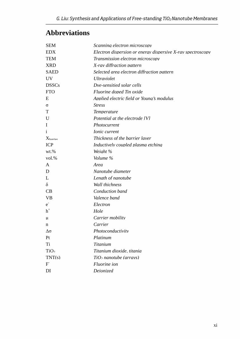
Abbreviations
SEM Scanning electron microscopyEDX Electron dispersion or energy dispersive X-ray spectroscopyTEM Transmission electron microscopyXRD X-ray diffraction patternSAED Selected area electron diffraction pattern UV UltravioletDSSCs Dye-sensitied solar cellsFTO Fluorine doped Tin oxideE Applied electric field or Young’s modulus σ StressT TemperatureU Potential at the electrode [V]I Photocurrenti Ionic currentXbarrier Thickness of the barrier layerICP Inductively coupled plasma etchingwt.% Weight %vol.% Volume %A AreaD Nanotube diameterL Length of nanotubeδ Wall thichnessCB Conduction bandVB Valence bande- Electron h+ Holeμ Carrier mobilityn CarrierΔσ PhotoconductivityPt Platinum Ti Titanium TiO2 Titanium dioxide, titania TNT(s) TiO2 nanotube (arrays)F- Fluorine ion DI Deionized

G. Liu: Synthesis and Applications of Free-standing TiO2 Nanotube Membranes
1
1 Introduction
1.1 Background
TiO2 is a wide band gap semiconductor, which has been broadly studied in water
splitting [1, 2], dye sensitized solar cells (DSSCs) [3, 4], photocatalysis [5, 6] and
sensors [7, 8] on the basis of its chemical stability and unique functional properties.
Compared with dense nanoparticles, TiO2 nanotubes (TNTs) are suggested to be
superior in chemical and optoelectronic performance due to its one-dimensional channel
for carrier transportation, in which the recombination of e-/h+ is expected to be reduced
[4, 9]. Of a variety of TiO2 synthesis strategies, particular interest has been given to the
anodic oxidized growth of TNT layers on Ti foil, as it leads to an array of closely
packed vertically aligned tubes [9, 10]. Growth of highly ordered TNTs with a length of
a few hundred nanometres has been first reported using electrochemical anodization of
Ti foil in aqueous hydrofluoric acid solution [11]. Very high aspect-ratio TNTs grown up
to hundreds of micrometres in length were also obtained through anodization of Ti in
organic electrolytes [12]. However, the nature of TNT arrays attached to an opaque Ti
substrate and with a closed bottom has restricted their feasibility for use in extensive
applications [10, 13]. Recent studies imply that free-standing TNT membranes have
more interesting performance than that of the TNT layer on Ti foils [13]. Key features
of free-standing TNT membranes lie on their absence of barrier layer at the tube bottom,
direct electrons transferring, stability to mechanical vibrations and they can be
integrated or transferred on any foreign substrates, which making them ideal structures
for a spectrum of applications in energy and environmental areas.
1.2 Application status
Integration of TNT membranes on the transparent and conductive substrate is an
efficient strategy. The best photovoltaic performance of DSSCs based on TNT
membranes reached 8.80%, which is higher than that of a TiO2 nanoparticle
G. Liu: Synthesis and Applications of Free-standing TiO2 Nanotube Membranes
2
electrode (7.58%) because of the reduced electron combination and efficient light-
harvesting efficiency [14, 15].
The free-standing TNT membrane with open-ends shows an increased efficiency in
water splitting. A maximum conversion efficiency of 0.70% was obtained with the
open-ended TNT membrane/FTO, which was much higher than the 0.22%
efficiency obtained by the closed-ended TNT membrane/FTO or 0.36% by the TiO2
particle/FTO electrode [16].
The TNT-membrane sensor is more sensitive than that of the membrane adhered on
Ti substrates. The variation of the resistance of a 25 µm thick free-standing TNT
membrane reaches 25 times when it is exposed to 1000 ppm hydrogen for 1800s, in
contrast to 11 times for the films on Ti substrate. The blocking layer that formed
between the TNT and the Ti substrate after annealing should be the main reason
account for the difference in sensitivity. Besides, the response of the free-standing
membrane is much quicker than that with Ti substrate due to which provides flow-
through channels that accelerate the diffusion of H2 into the nanotubes [17].
A cocatalyst loaded TNT membrane for high rate photocatalytic conversion of CO2
and water vapor into hydrocarbon fuels is demonstrated. With this assembly coupled
with an outdoor global AM 1.5 sunlight, hydrocarbon production rate of 111 ppm
cm-2 h-1 was obtained when the nanotube arrays are loaded with both Cu and Pt
nanoparticles. This rate of CO2 to hydrocarbon production is at least 20 times higher
than previous published reports. The high CO2 adsorption capacity was ascribed to
the synergetic effect of the high surface area tubular morphology and the mixed-
valence nanoparticles [18, 19].
A free-standing and flow-through TNT membrane has been designed for a novel
reactor. Via bleaching methylene blue solution under UV irradiation, the membrane
exhibits higher photocatalytic activity than the one with closed-ended. The
decomposition rate was determined by the diffusion rate, complete pollutant
removal was observed by one flow-through cycle through the membrane [12, 20].
A novel type of artificial K+-gated ion channels based on titania nanotube membrane
loaded with Au nanoparticles and G-rich DNA composite structure was developed.
This fabricated permselective membrane using K+ as a trigger may set light to the
field of biosensing, drug-release, ion exchange membrane and so on [21].

G. Liu: Synthesis and Applications of Free-standing TiO2 Nanotube Membranes
3
1.3 Aims and Tasks
From the literature survey, we concluded that TNT membranes demonstrate remarkable
behaviors that warrant further study, underlying the large number of researchers
working in this field. The exciton dissociation and carrier transportation are the two key
taches restricting the performance of optoelectronics. To obtain better performance,
increasing the active area of materials in devices and restricting the transport direction
of carriers to make sure of their directional transportation are straightforward strategies.
In this thesis, we follow the point of tailoring materials at nanoscale toward the
challenges, focus on synthesizing free-standing crystalline TNT membranes from Ti
foils for developing cost-effective and high performance optoelectronics. Apart from
meeting both requirements perfectly, an added value of this work is that it provides
physical insight into the photoconductivity of TNT network and presents an important
advance toward the integration of nanomaterials for optoelectronic applications.
1.4 Outline of thesis
The thesis is organized based on the published and submitted articles. The first chapter
“Introduction” presents the motivations fueled me to conduct the investigations and the
dissertation outline. In Chapter 2 “Summary of the articles”, five articles are collected.
All the articles are briefly introduced and discussed. Each article represents a stage of
my work. These articles are textured in a systematic way to show the progress of the
research step by step. The full-length articles are enclosed at the end of thesis. In
Chapter 3 “Conclusions”, contribution of this work to science is summarized.

G. Liu: Synthesis and Applications of Free-standing TiO2 Nanotube Membranes
5
2 Summary of the articles
In this section, five articles are selected to highlight the research content during Ph.D.
studies. The research consists of three packages: (1) an overview of all technologies to
prepare TNT membranes in Article I; (2) Experimental fabrication of TNT membranes
in Article II and Article III; (3) Photoconductive study of TNTs in Article IV and Article
V; The collected articles are organized in terms of the research stage, rather than the
publication date. The full-length articles are enclosed at the end of thesis.
2.1 Literature review (Article I)
The as-prepared TNT membrane adhered on opaque titanium foil restricts their
feasibility for many applications, such as tube filling, molecular separations and
catalysis, where flow-through of the nanotubes arrays is required [13, 20, 22]. The
physical properties and morphology of an open-end membrane depends on the specified
process parameters [23-25]. Normally, large residual stresses are introduced by specific
processes. Highly stressed membranes accumulate large amounts of strain energy. When
the strain energy release rate exceeds the interfacial toughness of the membrane,
delamination ensues and peels off from the surface [26]. Residual stress in thin
membranes comprises two main components: (i) thermal stress due to mismatching of
coefficients of thermal expansion of film and substrate materials and (ii) intrinsic stress
due to all other factors, like chemical reactions, ion diffusion, lattice mismatch or
different material properties etc. If the membrane is prepared at temperature of T, and To
is room temperature, Em is Young’s modulus, vm is Poisson’s ratio of the membrane
material, then assuming E and v to be temperature independent, this stress is written as
[26]
G. Liu: Synthesis and Applications of Free-standing TiO2 Nanotube Membranes
6
(1 ) o
Tm
th m substrateTm
EdT
(1)
where m and substrate are the coefficients of thermal expansion of the membrane and
substrate, respectively. Values of elastic constants and thermal expansion coefficients of
Ti / TiO2 are Ti = (9.41~10.03)×10-6/ OC, TiO2 = 8.7×10⁻⁶/ OC, vTiO2 = 0.28, ETiO2 =
282.76 GPa. But the real mechanism behind the detachment process is complicated and
not well understood as yet. Herein, typical methods to detach the TiO2 nanotube
membrane and make it capable of flow-through are discussed in this section. The
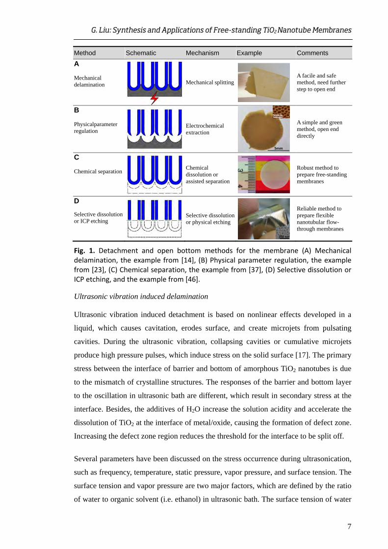
related techniques and mechanism are sketched as in Fig.1.
2.1.1 Mechanical delamination (Fig.1A: Solvent evaporation / Ultrasonic vibration / Peeling-off by tape)
Solvent evaporation induced delamination
Methanol [12, 27, 28] and DI water [29] are commonly used rinsing liquids and
solvents. A possible detachment mechanism of solvent evaporation induced free-
standing membrane is understood as multilayer delamination (Fig.1, method A).
Although the nanotube membrane surface is rinsed and kept in an organic bath after
electrochemical anodization, a small amount of H+ and F- still remain in the regions
between adjacent nanotubes. A slow etching caused by the remaining H+ and F- ions led
to structural defects. Moreover, rinsing the sample with liquid methanol (surface tension
~22.1dynes/cm at room temperature), the liquid diffused into the interpore regions and
wet the defect surface [28]. Subsequently, slow evaporation in the defect areas induces
the delamination of the barrier layer driven by the surface tension.
After rinsing the prepared sample with solvents, a mild ultrasonic in methanol is often
adopted to get rid of nanofibrous debris on the surface. The cleaned membrane is then
left to dry in air with the anodized surface facing up. A brownish colored membrane is
then separated from the Ti foil during the evaporation of the methanol. A gentle
mechanical bending of anodized Ti foil facilitates complete detachment of the
membrane [28]. The membrane dimension is flat in wet conditions, dramatically
cracking, fracturing, and curling into many small pieces during drying in atmosphere. It
is believed that a combination of both surface tension forces and strain gradients
account for this curling. To overcome the curling, super critical point drying was
proposed to prepare flat, mechanically robust membranes [12].
G. Liu: Synthesis and Applications of Free-standing TiO2 Nanotube Membranes
7
Method Schematic Mechanism Example Comments
A Mechanical delamination Mechanical splitting
A facile and safe method, need further step to open end
B Physicalparameter regulation
Electrochemical extraction
A simple and green method, open end directly
C Chemical separation
Chemical dissolution or assisted separation
Robust method to prepare free-standing membranes
D Selective dissolution or ICP etching
Selective dissolutionor physical etching
Reliable method to prepare flexible nanotubular flow-through membranes
Fig. 1. Detachment and open bottom methods for the membrane (A) Mechanical delamination, the example from [14], (B) Physical parameter regulation, the example from [23], (C) Chemical separation, the example from [37], (D) Selective dissolution or ICP etching, and the example from [46].
Ultrasonic vibration induced delamination
Ultrasonic vibration induced detachment is based on nonlinear effects developed in a
liquid, which causes cavitation, erodes surface, and create microjets from pulsating
cavities. During the ultrasonic vibration, collapsing cavities or cumulative microjets
produce high pressure pulses, which induce stress on the solid surface [17]. The primary
stress between the interface of barrier and bottom of amorphous TiO2 nanotubes is due
to the mismatch of crystalline structures. The responses of the barrier and bottom layer
to the oscillation in ultrasonic bath are different, which result in secondary stress at the
interface. Besides, the additives of H2O increase the solution acidity and accelerate the
dissolution of TiO2 at the interface of metal/oxide, causing the formation of defect zone.
Increasing the defect zone region reduces the threshold for the interface to be split off.
Several parameters have been discussed on the stress occurrence during ultrasonication,
such as frequency, temperature, static pressure, vapor pressure, and surface tension. The
surface tension and vapor pressure are two major factors, which are defined by the ratio
of water to organic solvent (i.e. ethanol) in ultrasonic bath. The surface tension of water
G. Liu: Synthesis and Applications of Free-standing TiO2 Nanotube Membranes
8
and ethanol is 72.75×10⁻³ and 22.32×10⁻³ N/m, while the vapor pressure is 17.5 and
44.6 mm Hg at 293 K respectively [17]. Thus, adding a certain amount of water in
ethanol increases the solution acidity as well as enhances the surface tension. Applying
ultrasonic vibration in a solution of water and ethanol with 1:4 volume ratios and
followed by drying in atmosphere, a large-area and non-collapsing free-standing thin
TiO2 nanotube membrane was detached from Ti substrate [17]. In even lower water
concentration, ultrasonic agitation in 95% ethanol solution for several minutes, a thicker
TiO2 nanotube membrane was detached due to the low acidity, and the bottom ends of
the membrane were opened in a 5 wt% NH4F-1M H2SO4 solution for 15 min [30, 31].
Direct peeling-off by tape
Peeling-off by Scotch tape is a straightforward method to separate inorganic TiO2
membrane from Ti foils by mechanical force [32]. However, the detached membrane are
easily curled or broken since the flexibility of the tape. Another better solution for
fabricating self-supporting membranes is to detach the oxide films with an adhesive
polymer, followed by soaking it in organic solvent to remove the polymer. Alternatively,
the transfer printing technique developed by Rogers and co-workers was applied to
detach the nanotube membrane [33].
2.1.2 Physical parameter regulation (Fig. 1B: Voltage, Temperature, Electrolyte composition)
Voltage control
Decreasing and increasing voltage at the end of the anodization reduce adhesion of TiO2
nanotube layer on Ti substrate, and simultaneously open up the bottom ends [23, 25, 34-
36]. This method is attributed to local acidification and gas evolution produced by
voltage transition. Through the voltage transition at the end of anodization, the bottom
end morphology was tailored by tuning the magnitude and duration of the anodized
voltage and the barrier layer at the bottom becomes fragile. Thus, both the breaking
away of the TiO2 nanotubes from the Ti foil and the opening of their bottoms can be
easily achieved. This method is simple and offers a number of advantages in
comparison to chemical etching by HF.
As an example of this technique, a constant voltage of 100 V for 2-3 h in NH4F/ethylene
glycol electrolyte was carried out by using computer controlled power supply. At the
end of the process, the voltage was decreased by software or manually adjusted

G. Liu: Synthesis and Applications of Free-standing TiO2 Nanotube Membranes
9
potential to 10 V, over 0.5-1 minute. Following the fabricated TiO2 nanotube layer was
detached by sonication in a methanol bath, and membranes with through-hole
morphology were observed [23]. In our recent experiment, the immobilized membranes
with ordered TiO2 nanotube arrays are prepared in ethylene glycol electrolyte under
60V/24 h first, then after annealing at 500 OC for 2 h, followed by another anodized at
20, 60, 100 V for 60, 30, 10 minutes, respectively. All of the membranes were
successfully detached from the substrate by taking advantage of the different
mechanical stress of the two anodic layers [25]. On the contrary of decreasing the final
step voltage, free-standing and flow-through TiO2 nanotube layers were also observed
by raising the voltage from 60 V to 80-180 V at the end of process [34-36].
Temperature control
A thermal treatment has been applied for as-prepared TNT membrane on titanium foils
to assist membrane detachment [22, 25, 37]. The process is described as three steps [37].
First, the Ti substrate is electrochemically pre-anodized. Then the pre-anodized TiO2
layer is peeled off by intense sonication in deionized water to expose the
electrochemically patterned Ti substrate. The patterned substrate Ti is then anodized
once more, and the new oxide layer is heat-treated at a temperature range of 200-700 OC.
The initial two electrochemical anodization steps were carried out at 10 °C in electrolyte
while the third one at an elevated temperature 30-50 OC. The free-standing membranes
are completely detached by the third step.
This method utilized the different mechanical stability and etching selectivity between
upper and lower tube layers [22, 38]. After thermal treatment, anatase crystals formed
on the upper layer show high resistance to chemical etching. While the bottom tube
layer formed by third-step anodization has an amorphous structure. Therefore, the
crystallized TiO2 layers can easily be mechanically peeled off by taking the advantage
of the different material properties between the anodic layers. The elevated bath
temperature is crucial for the membranes separating. The high temperature at the third
step gives rise to low viscosity and high current density for the electrolyte, which leads
to enhanced chemical etching ability. Local chemical dissolution is expected to be fast
for newly formed TiO2 nanotubes, which has less dense walls at the interface and weak
interconnection.

G. Liu: Synthesis and Applications of Free-standing TiO2 Nanotube Membranes
10
Electrolyte composition control
By regulating the composition and concentration of electrolytes, detached TiO2
nanotube array membranes were achieved directly due to etching contrast between the
oxide layers and the substrate [39, 40]. As sodium molybdate (0.1M) was added in
ethylene glycol solution containing 2% water and 0.5% ammonium fluoride, free-
standing transparent TNT membranes were synthesized. The membrane was amorphous
TiO2 with thickness equal to 10 µm. After a hydrothermal treatment at 120 OC,
amorphous TiO2 nanotubes were transformed to anatase structure while the integrity
structure of the membranes was maintained [40].
2.1.3 Chemical separation (Fig. 1C: Chemical dissolution/Chemical assisted separation)
Chemical dissolution
A dense and free-standing membrane consisting of both-side-open TiO2 nanotubes was
detached from metallic Ti substrate by chemical dissolution process [20]. In this process,
a high aspect ratio TiO2 nanotubular layer was first prepared on Ti substrate. Then the
specimen was immersed into a mixture of Br2 and dry methanol for 12h in N2
atmosphere. This created a free-standing nanotube membrane floating in the etching
solution. After being rinsed with methanol and DI water, the layers were placed (closed
tube side down) above an open bottle containing HF 48% for preferential etching of the
tube ends. Finally, the sample is rinsed with DI water again. The final membrane allows
direct, size-selective, flow-through photocatalytic reactions with high efficiency.
However, this fabrication method takes long process time and used a toxic bromine-
containing methanol solution.
Chemical assisted separation
The solutions H2O2, HCl, HF and HgCl2 have been employed for chemical assisted
separation of TiO2 nanotubes membrane from Ti substrates [16, 37, 41-45]. The as-
prepared nanotube array membranes and Ti substrate were immersed in 33 wt% H2O2
solution for tens of second, following which the entire TiO2 nanotube membrane was
lifted off from the Ti substrate with a closed ends [16, 41]. Then, oxalic acid was used to
remove the tube ends. During this wet-chemical etching, a thin layer of hot-melt
adhesive was used as a protective layer to cover on the opened top of the nanotube
arrays for retaining its tubular structure first. The free-standing array membrane was

G. Liu: Synthesis and Applications of Free-standing TiO2 Nanotube Membranes
11
then immersed in 0.5% oxalic acid solution at 40 OC for a certain time. Titanium oxide
located at the interface of the tube and the bottom ends was etched by oxalic acid to
form a yellow titanium oxalate complex. After the bottom ends fell off and the open
pores appear, the thin protective layer was separated by soaking the adhesive in acetone
solution [16].
An alternative method is that amorphous TiO2 nanotube layer is crystallized by high-
temperature annealing at 330-500 OC in oxygen ambient. Then a thin underlayer of
amorphous nanotube layer is grown underneath the annealed TiO2 nanotube layer by a
secondary anodization step. Next, the amorphous lower-layer is selectively dissolved by
a treatment in 5% H2O2 solution for 12 hours. The crystallized titania nanotube
membrane present an excellent anticorrosion ability in the solution and was separated
from the Ti substrate without any cracking [37].
Etching bottom layer in 0.1 M aqueous HCl solution for 1 hour is another option to
prepare free-standing membranes [43, 44]. The free-standing membrane was
manipulated with tweezers and transferred onto fluorine doped tin oxide (FTO) glass
substrate. Besides, free-standing TiO2 nanotube membrane was peeled off by soaking
the films in a saturated HgCl2 solution for several hours, leaving self-supporting
membrane and the titanium substrate [45].
2.1.4 Selective dissolution or ICP etching (Fig. 1D: Selective dissolution/ ICP etching)
Selective dissolution
This technique consists of anodizing a pre-formed metallic double layer Ti/Al and
followed by a wet etching technique. The electrochemical parameters are adjusted to
allow for nanotube formation in metallic Ti layer. Once the thin Ti layer is fully
anodized, it continues to etch into the underlying aluminum layer. The anodized double
layer (Ti/Al) membranes are then immersed in ethanol and dried in air. Last, the
aluminum and formed alumina pores are selectively removed in an acidic etchant. Albu
et al. have demonstrate the fabrication of a large-scale, flexible and well electrically
connected nanotubular flow-through TiO2 nanotube membranes by taking this technique
[46]. This strategy allowed large-scale membranes to be reliably fabricated for the first
time. A prior photolithographic definition of pore-array squares shows much advantage
to provide rupture-free structures, mechanical flexibility, and high conductivity via the
G. Liu: Synthesis and Applications of Free-standing TiO2 Nanotube Membranes
12
remaining Ti metallic frameworks. An alternative approach to prepare TiO2 nanotube
arrays with through-hole morphology by anodizing a thermally evaporated Ti/Au
bilayer film also have been demonstrated [47].
ICP etching
Inductively coupled plasma etching uses reactive plasma to micro machine
semiconductor materials. High-energy ions from the plasma attack the materials and the
plasma-assisted reaction produce volatile compounds which are pumped out from the
ICP system. Thus, the barrier layer at the bottom of the titania nanotube arrays could be
removed by ICP etching to get flow-through titania nanotube arrays [21, 48]. For
instance, the flow rate of plasma etching parameters were He 20 sccm, Cl2 10 sccm,
BCl3 40 sccm with a base pressure equal to 0.8-0.9 Pa. After plasma etching for 10 min,
the bottom ends of the titania nanotube arrays were completely opened [21]. Compared
to previous attempts, these approaches are scaled up to large areas and eliminate the
critical bottom opening steps, and compatible with standard MEMS technology.
2.1.5 Advance in photoconductive studies of TNTs
The characteristics of photocarrier dynamics in semiconductors are the basis of the
operation of photodetectors, photodiodes, and solar cells, and they typically include
photogeneration of electron-hole pairs, their efficient transport, and collection as the
output signal. The photoconductivity in a semiconductor can be defined as photo e n ,
where e is the electronic charge, μ is the carrier mobility and Δn is the carrier
concentration [49-51]. Nanostructured materials are attractive for photon detection
because of their large active surface area and potential integration with conventional
electronics [49, 50]. In a semiconductor nanowire/ nanotube, the electron-irradiation-
carrier dynamics just like the photo-carrier dynamics could be strongly affected by
carrier trapping and/or scattering at the surface localized energy states over the bulk
energy states, particularly due to the large surface-to-volume ratio. Earlier examples of
semiconductor nanowire (Ge, ZnO) photodetectors indicate that the response process is
strongly influenced by temporal and spatial charge separation and carrier multiplication
within one dimensional confinement [51, 52]. The photoconductivity is size-dependent
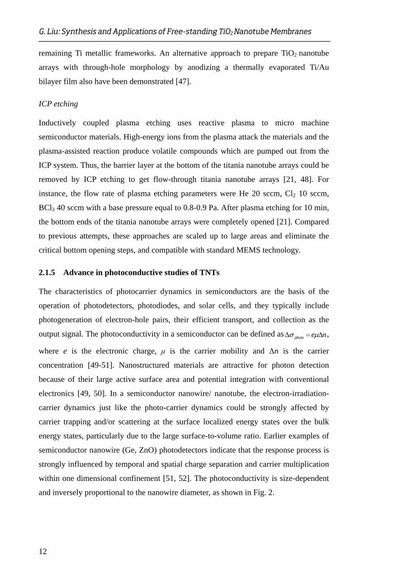
and inversely proportional to the nanowire diameter, as shown in Fig. 2.

G. Liu: Synthesis and Applications of Free-standing TiO2 Nanotube Membranes
13
Fig. 2. Diameter‐dependent photoconduction (a) illustration of the photocarrier generation by the low photon flux and subsequent electron surface trap and hole accumulation at the nanowire (NW) cross sections with different diameters, which is similar to a cylindrical capacitance. (b, c) Two‐dimensional simulation of the induced hole concentrations (filled colors) for 50 and 300 nm thick Ge NW cross sections. (b) The induced hole concentrations at lower photon flux as in the case of (a). (c) The induced hole concentrations in the case of full saturation of surface states upon the higher photon flux. Contours in each NW cross‐section image represent the equipotential line (gray). (d) Diameter dependence of the photoconductivity. (e) Diameter dependence of the photocarrier concentration when the gain is maximal [51].
TiO2 nanostructures such as nanotubes, nanowires/rods are one of the main groups for
the fundamental research and development of real-world nanoelectronics [4, 8-10]. The
distinctive UV absorption ability makes TiO2 suitable for UV detection against the
background of infrared and visible light [8]. The anisotropic geometry of the one-
dimensional structure facilitates rapid transport of carrier, which is crucial for
optimizing the carrier collection efficiency [53, 54]. Various aspects of TiO2
photodetectors have been addressed by downsizing from bulk to nanometer in literature.
Earlier studies are devoted to understand the dynamics of the transport, trapping and
recombination of charge carriers generated in TiO2 nanoparticle films [55, 56]. However,
it is a challenge to extract the intrinsic transport properties from the size effects in dense
a b
c
d e
G. Liu: Synthesis and Applications of Free-standing TiO2 Nanotube Membranes
14
nanoparticle films. Subsequent in situ observations of photoconduction properties over
the 1D TiO2 nanostructures provide a means of exploring the surface and size effects on
the electrical transport phenomena [53, 57-59]. Nevertheless, their manufacturing is
complicated and not suitable for large-scale applications. Recent studies are focused on
device performances by using TiO2 rods/tubes as building block that leads to a
filling/decoration of nanostructures [8, 54, 60, 61]. For such composites, it is difficult to
extract details on rod/tube-induced transport properties as that represents a mixture of
material behavior. Despite the progress, fundamental questions about the internal
electronic structure, the effect of the large surface or small size in comparison to its bulk,
and size dependent transport phenomena in TiO2 nanotubes remain scarcely answered
up to now.
2.2 Fabrication of TiO2 nanotube membranes
2.2.1 Amorphous free-standing TNT membranes (Article II)
In this work, we developed a facile procedure for fabricating free of disorder
nanostructuress, large-area, flat and mechanically robust TNT membranes. The major
highlights of this approach are (i) straightforwardly detaching a large scale TNT
membrane from Ti substrate after a single anodization step. (ii) Rinsing the as-anodized
film with ethanol effectively avoids the architectural disorder on the membrane surface.
(iii) Reducing evaporation rate of the rinsing solvent assures the detachment of a large
area, flat surface and free-standing membrane.
Experiment
Prior to anodization, Ti foils were cut into required size (~15mm×35mm×0.3mm, 99.8%
purity), and degreased by sonicating in acetone, isopropyl alcohol and methanol each
for 10 min. Then the Ti sheets were rinsed with DI water and dried in air. The
anodization was carried out in a two-electrode system with a platinum foil as a counter
electrode and Ti sheet as a working electrode. The distance between cathode and anode
was fixed to 3.5cm. Anodization was conducted at a constant voltage of 80V for 24 h at
room temperature. Ethylene glycol (99.8 wt%, Sigma-Aldrich) containing 0.5 wt%
ammonium fluoride and 0.3 wt% DI water was used as the electrolyte.
The fabrication processes are schematically shown in Fig. 3. A Ti foil (Fig.3a) is
anodized to form TNT arrays (Fig. 3b). The as-prepared arrays are rinsed by ethanol and
G. Liu: Synthesis and Applications of Free-standing TiO2 Nanotube Membranes
15
then covered by a piece of heavy duty cleanroom paper (TX5729) to assure a slow
evaporation (Fig.3c). Last these TNT arrays are self-detached from the substrate during
evaporation process and result in a flat free-standing TNT membrane (Fig. 3d). As a
comparison, another as-anodized sample was rinsed with DI water and drying in the air.
Furthermore, the membranes were annealed to obtain the crystalline phases.
Fig. 3. Schematic illustration of the fabrication process
The morphology and the structural quality of membranes were investigated by scanning
electron microscope (SEM, Philip EX-30) and transmission electron microscope (TEM,
JEM-2010HR). The TNTs were scratched from the sample and dispersed in ethanol, and
one drop of the suspension was dropped onto a carbon-coated copper grid for HRTEM
and SAED measurements. The crystal structure of membranes was identified by X-ray
diffraction (XRD, Bruker AXS D8 Discover) using Cu Kradiation.
Discussion
Fig. 4 (1) and (2) show photographs of the obtained free-standing TNT membranes. The
membrane (Fig. 4 (1)) was rinsed by DI water and dried in atmosphere [34], the free-
standing TNT layer was detached from Ti substrates during the water evaporation. The
surface of the membranes was flat in wet status while they dramatically cracked and
curled into small pieces after drying. From the top-view SEM image in Fig. 4(a), it can
be seen that both clusters of TNT bundles and microcracks exist in the membrane
structure. The disorder nanowires (inset in Fig. 4(a)) were caused by the nanotube
lateral deflection resulting from the action of capillary forces between adjacent
Ti foils Oriented TNT layer
Large-scale, flat free-standing TNT membranes
(c)
Anodization
Rinsed with ethanol
(d)
A TX5729 paper
Evaporation at room temperature
(b) (a)
G. Liu: Synthesis and Applications of Free-standing TiO2 Nanotube Membranes
16
nanotubes during evaporative drying. The extents of bundling and crack are supposed to
increase with increasing the membrane thickness [62, 63]. Fig. 4b displays the cross-
section SEM image of the membrane. The TNT length is about 300m. The tube tips
are sparse while the bottom parts are closely connected, a combination of both surface
tension forces and strain gradients account for the curling [34].
The anodized TNT membrane rinsed with ethanol, and then covered by a piece of heavy
duty cleanroom paper to slow down the evaporation rate. After drying and removing the
paper, a free of disorder nanostructures, large scale, free-standing and mechanically
robust TNT membrane was observed, as shown in Fig. 4(2). The large area detachment
of the TNT membrane can be understood through the low drying rate, which induces the
tension force between the membrane and metallic substrates to be released uniformly.
Although a free-standing TiO2 nanotube membrane was developed based on methanol
wetting and subsequent N2 blow-dry technique [64], the N2 air turbulences along the
blowing streams might obsess the fragile membranes to reach a large scale. Moreover,
ultrasonically cleaning the surface induced unevenly strain and tension forces over the
whole membrane and easily crumbled the membrane into small pieces [28]. In contrast,
ethanol has a relatively low surface tension and evaporation rate; herein the whole
membrane remains an intact and flat surface after drying. It can be seen from the top-
view SEM image (Fig. 4c) that the amount of morphological disorder was significantly
reduced. The magnified image (inset of Fig. 4c) shows that the TNT arrays remain
compact, stand vertically and no destructive changes are observed after peeling from the
Ti substrate. The constituted TNTs are of an average diameter of 150 nm and wall
thickness of ~15 nm. Fig. 4d shows cross-section SEM image of the membrane, where
the TNT length is about 300m. The estimated aspect ratio (length/diameter) of the
membrane is ~ 2000, which is an important parameter for photoelectrochemical
application [10, 28].
G. Liu: Synthesis and Applications of Free-standing TiO2 Nanotube Membranes
17
a
1m
c
1m
d b
Fig. 4. Digital photographs of free‐standing TNT membranes rising with (1) DI water or (2) pure ethanol. SEM images of the membranes cleaned with water (a) top‐view, (b) cross‐section, cleaned with ethanol (c) top‐view, (d) cross‐section.
Fig.5 presents an angle-view photograph and detailed SEM images (insert) of a large
scale, flat, free-standing TNT membrane and the corresponding Ti substrate. The
membrane is mechanically robust and can be easily manipulated with tweezers, standing
perpendicularly without any bending. The surface SEM image (insert Fig.5a) shows an
ordered and compact nanotube array rather than disordered nanowire structure. The
cross-section image (Fig. 5b) illustrates that these pores are consisted of densely packed
nanotubes. This vertically oriented, close-packed morphology of nanotube arrays go
(2) (1)
G. Liu: Synthesis and Applications of Free-standing TiO2 Nanotube Membranes
18
straightly from the top to bottom of the membrane and provide a direct pathway for
electron transport at the nanotube walls. The bottom image of the membrane and the
remained footprint on the substrate are presented in Fig. 5c, d, respectively. It can be
seen that the membrane bottom consisted of close-packed TNTs with a closed end. The
diameter of the end is ~200 nm and a barrier layer existed between the TNTs and the Ti
substrate.
Specifically in the barrier layer, the ions migrated through the oxide film and upon
arrival at the oxide-metal interface forms a sacrificial soluble oxyfluoride layer. This
thin layer consists of various anions (F-, O2-, OH-) and metal cations Tin+ combined in
many different ways. Prior study indicated that the relatively fast migration of fluoride
ions as compared to other ions (such as O2-) account for the poor adhesion between the
oxide membrane and the underlying substrate [32]. Therefore, the applied voltage is the
dominant factor to the growth and the self-detached process of TNT arrays. Generally,
low voltage (0-40 V) results in an immobilized TNTs with thin thickness, high voltage
(>80 V) and long duration cause over-etching on the surface, leading to disorder
nanostructures left on the surface [65-67]. Thus, the membrane fabrications were all
conducted in the potential range of 40-80 V [34-42, 68], but few researcher emphasized
this critical step. In this study, anodization at 80 V for 24 hours was proved to be
balance the material contrast and the growth rate of the TNT tube. As a result, it not
only produced the membrane with enough mechanical strength but also led to a facile
detachment.

G. Liu: Synthesis and Applications of Free-standing TiO2 Nanotube Membranes
19
Fig. 5. Self‐standing TNT membranes (a) top view (b) cross‐section (c) bottom view (d) corresponding foot print left on the substrate
The phase of TNT arrays is amorphous after electrochemical anodization. High
resolution transmission electron microscope (HRTEM) image (Fig. 6a and c) shows a
disorder amorphous characteristic. A large number of localized states in the amorphous
structure can act as traps and recombination centers [69-71], which reduce the TNT
performance (e.g. photo-catalytic/electronic). To crystallize the titanium dioxide, the
TNTs were annealed in air with the temperature ramping at a rate of 2 °C/min and then
kept at 500 °C for 2 h. Crystallized and ordered structure of the TNT is immediately
apparent after annealing, as shown in Fig. 6b and d. XRD characterization (Fig. 6e)
further confirmed that the as-prepared TNT is amorphous and no obvious peaks can be
found. On the contrary, the crystallized counterpart shows three strong diffraction peaks.
All reflections are indexed (marked by black bar in Fig. 6e-JCPDS file 84-1286), the
diffraction peaks at 2θ= 25.5°, 38.1°, 48.3° can be identified to the (101), (004), (200)
crystal faces, respectively. The grain diameter estimated from TEM analysis is 80 nm
while Scherrer analysis of the X-ray patterns give a value of 82 nm from the (101)
diffraction peak.
a
b
c
d
Ti substrate
TNT membrane

G. Liu: Synthesis and Applications of Free-standing TiO2 Nanotube Membranes
20
2 (degree)10 20 30 40 50 60 70 80
Inte
nsity
(a.
u.)
anatase
amorphous
(101
)
(20
4)
(21
1)
(10
5)
(20
0)(0
04
)
(21
5)
(220
)(1
16
)
(10
3)
(112
)
(21
3)
(10
7)
Fig. 6. TEM images of the amorphous (a) and anatase TNT (b), (c) and (d) are the selected area electron diffraction (SAED) patterns, (e) XRD patterns of the TNTs
2.2.2 Free-standing crystalline TNT membranes (Article III)
In this paper, a handy experimental procedure was proposed to fabricate free-standing
crystalline TNT membranes. The concept is outlined in Fig. 7 (1)-(4). The ordered TNT
arrays are firstly fabricated under optimized parameters, after an annealing and followed
by a second (detachment) anodization step, free-standing crystalline TNT membranes
are detached from the substrate without any cracks. Low detachment voltage (20V)
c d
e
a b
G. Liu: Synthesis and Applications of Free-standing TiO2 Nanotube Membranes
21
results in closed end membranes, while through-hole membranes are obtained at a high
detachment voltage (100V). This method is a reliable technique for fabricating free-
standing TNT membranes without the needs for any complicated processes or
dangerous chemicals. At the same time, different from previous studies, we have
systematically investigated the effects of voltage on the detachment process of free-
standing crystalline TNT membranes.
Experiment
Ti foils were cut into required size (~15mm×35mm×0.3mm, 99.8% purity, obtained
from Baoji Titanium Industry Co., Ltd, China), degreased and cleaned by sonication in
acetone, isopropanol and deionized water for 10 min during each step. After drying, the
backside of Ti foil was covered by a Scotch tape, rinsed by water and exposed to UV
radiation about 10min for cleaning. Then it was put into a polyflon cell with an area of 4
cm2 exposed to the electrolyte. Ethylene glycol with 0.5 wt% ammonium fluoride
(NH4F) and 3 vol% water was used as electrolyte. The first anodization was started with
growth of ordered TNT arrays on Ti foil under 60V for 24 h, followed by sonic cleaned
in ethanol to remove the electrolytes and annealed at 500 OC for 3 h to crystallize the
TNT arrays. Then, the annealed samples were anodized again in the same stock
electrolyte with another voltage (e.g. 20, 60, 100 V). After detecting the detachment
occurs over time to each case, the samples were picked out and rinsed by ethanol to
remove the electrolytes, finally dried in air. The morphology of the TNT membranes
was characterized by a Philip EX-30 scanning electron microscope (SEM). X-ray
diffraction analysis (Bruker AXS D8 Discover with a normal θ-2θ scan, Cu-Kα
radiation) was performed for phase identification.
Results and discussion
Fig.7 (a-c) shows the photographs of free-standing crystalline TNT membranes and
their substrates with various detachment voltages (second anodization). The membrane
geometry was defined by the first anodization (60V/24 h) [45, 72], but the applied
voltages in second anodization step were 20, 60 and 100 V respectively, corresponding
to the sample a, b and c. It can be seen that the membranes formed with white color, free
of cracks and only slightly bending upon air drying. This bending effect may be
ascribed to the absence of barrier layer at tube bottom, where compressive stress is
exerted.

G. Liu: Synthesis and Applications of Free-standing TiO2 Nanotube Membranes
22
Fig. 7. Schematic illustration of the fabrication process for free‐standing crystalline TNT membranes (1)~(4) and (a~c) the three resulting samples are firstly anodized at 60V/24h, then annealing at 500 OC/3 h, followed by another anodization at 20V/60 min, 60V/30 min and 100V/10 min, respectively.
Fig. 8 shows the top view, cross section and bottom view SEM images of the above
three membranes. From the top view and cross section images in Fig. 8a-c, it can be
observed that all membranes (the inserts of Fig. 8 a-c) display a thickness of 18 m and
the average inner diameter of 140 nm, which are not influenced by the second
anodization step. This phenomenon indicates that crystallized layer shows high
resistance to chemical etching from the electrolyte. Fig.8 d-f shows the surface of Ti
substrates after detachment and bottom morphology of the membranes. It can be seen in
Fig.8d and its insert that the membrane detached at low voltage (under 20 V for 60
minutes) preserves their tube morphology and the bottom of tubes are closed, and a non-
ordered compact oxide layer is present on the bottom of membrane. As shown in Fig. 8e,
the nanotube bottom ends are opened partly in 30 minutes with the detachment voltage
Crystalline TNTs Crystallized, free-standing
(3) (4)
2nd layer of amorphous TNTs 2nd anodization
a b c
Ti foils
1st layer of amorphous TNTs
1st anodization
Annealing
(1) (2)

G. Liu: Synthesis and Applications of Free-standing TiO2 Nanotube Membranes
23
equals to 60 V. On the other hand, all bottom ends of the nanotube are homogenously
opened at the high detachment voltage (100 V), and the through-hole diameter is about
50 nm as present in the inset of Fig. 8f. Besides, the detachment process at high voltage
is faster than that of the low voltage, and it only needs about 10min.
To clarify the detachment mechanism of the free-standing TNT membranes, top-view
SEM images of the membranes (Fig. 9a-c) and the images of underlying TNT layer
remaining on substrate (Fig. 9d-f) were further analysed. We can see that the tip wall
thickness of the TNT on membrane is about 15nm. However, the wall thickness and
inner diameters of the underlying tube on substrate are 10, 25, 45nm and 30, 60, 80 nm
corresponding to the 20, 60 and 100 detachment voltage, respectively. The interface
structures of membranes before detachment might be presumed as the schematic
diagrams in Fig. 9. The possible detachment mechanism of the TNT arrays from the
substrate can be explained as follow: a TNT layer prepared under a set of parameters
leads to a specific geometry, the underneath layer may be initiated at the bottom of a
tube [34, 73-76], or in the spaces between the tubes [73]. The crystallized/amorphous
oxide interface forms from various anions (F-, O2-, OH-) and metal cations Tin+
combined in different ways. The relatively fast migration of fluoride ions as compared
to other ions (such as O2-) induced a poor adhesion between the layers [32].
G. Liu: Synthesis and Applications of Free-standing TiO2 Nanotube Membranes
24
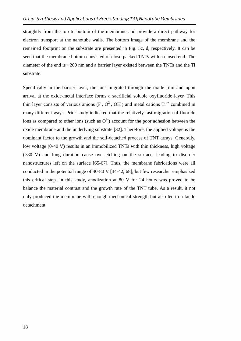
Fig. 8. (a‐c) Top view, cross‐section (inert) and (d‐f) bottom view images for the membrane a~c in Fig.7.
Furthermore, different from previous studies, the local acidification and gas evolution
produced by transition voltage [34] and mechanical contrast account for the detachment
of present study. Therefore, all methods can effectively detach the TNT membrane. But
the membrane detachment more likely occurs below the interface (as marked by blue
dash-line) at low voltage and above the interface at high voltage due to sharp contrast of
material properties and the resulting structure. To the middle voltage (60V), the
detachment is random distributed over the interface.
a
Closed end with
oxide layer
Open end
closed end
Open end
b
c
d
e
f
1m
1m
Closed end with
oxide layer

G. Liu: Synthesis and Applications of Free-standing TiO2 Nanotube Membranes
25
Fig. 9. The presumed structure before detachment, (a~c) top view images of the membrane and (d~f) the left layer on corresponding substrates.
X-ray diffraction (XRD) patterns were further used to characterize the crystal structure
of the membranes. Standard patterns of Ti (JCPDS file 44-1294) and anatase TiO2
(JCPDS file 84-1286) were plotted in Fig. 10 for comparison [71]. It shows that the
preferential crystallographic orientation of the metallic Ti substrates is (103), the grain
size of the underlying titanium substrate evaluated by Scherrer equation is about 194.8
nm. The as-prepared TNT film is amorphous and only diffraction peaks of Ti can be
found in Fig. 10a. In general, as the annealing temperature increases from room
temperature to 800 OC, the phase of titanium oxide changes as amorphous→anatase→
rutile. To form anatase TiO2, annealing at 330-500 OC for 1-3h in an oxygen ambient is a
common procedure in literatures [71, 77, 78]. After calcination at 500 OC for 3 h, more
X-ray diffraction patterns are clearly observed in Fig.10b, which can be referred to
anatase phase.
Detachment
20V 60V 100V
2nd tube layer
1st tube layer
a b c
d e f
140nm 140nm
80nm60nm30nm
140nm

G. Liu: Synthesis and Applications of Free-standing TiO2 Nanotube Membranes
26
Inte
nsity
(a.
u.)
(a)
(b)
(c)
2 (degree)10 20 30 40 50 60 70 80
(10
0)
(002
) (101
)
(102
)
(11
0)
(103
)
(112
)(2
01)
(101
)
(20
4)
(211
)(1
05)
(20
0)(0
04)
(215
)
(220
)(1
16)TiO2 anatase
Ti
(103
)(1
12
)
(21
3)
(10
7)
Fig. 10. XRD patterns of (a) as‐prepared and (b) annealed TNT arrays on Ti substrates and (c) free‐standing crystalline TNT membranes.
In contrast, for the crystallized free-standing TNT membrane, the diffraction peaks of Ti
substrate disappear and all of the peaks can be attributed to the anatase TiO2 phase (Fig.
10c), the strong diffraction peaks at 2θ = 25.5O, 38.1O, 48.3O can be identified,
respectively, to the (101), (004), (200) crystal faces. The grain size of the anatase TiO2
is about 81.6 nm, which was supposed no relevance to the grain size of the Ti foil but
depended on the annealing temperature [69].
2.3 Photoconductive study of TiO2 nanotubes
2.3.1 Photoconductive, free-standing crystallized TNT membranes (Article IV)
In this paper, we demonstrate that high photoconductive gain is achievable through a
large-scale, free-standing crystallized TNT membrane. Schematic illustration of the

G. Liu: Synthesis and Applications of Free-standing TiO2 Nanotube Membranes
27
membrane fabrication via a two-step anodization and packaged device for the
photoconductive characterization is shown in Fig.11. The first anodization grows
ordered TNTs on a Ti foil, followed by annealing to crystallize the TNTs. Then, the
annealed sample is anodized again to create an amorphous TNT layer below the
crystallized layer, which is self-detached from the substrate to form a free-standing
membrane. Next, the membrane is transferred to a silicon substrate patterned with gold
interdigitated electrodes, and assembled with a quartz-glass cover to form a
photoconductive device. The contribution of this work are (i) evidenced the controllable
growth of free-standing TNT membranes, (ii) revealed the surface effects on the
electrical transport in TNT membranes, (iii) extracted intrinsic properties of the TNTs
from the effect of metal substrate and/or supporting electrolyte.
Fig. 11. Fabrication procedure (1) First anodization grows a layer of amorphous TNT. (2) Annealing the TNT layer. (3) Second anodization to grow a beneath layer of amorphous TNT and meanwhile detach the first layer. (4) Transfer the membrane to a substrate with gold electrodes. (5) A complete TNT‐membrane device.
Experimental Details
1. Synthesis of TNT membrane
Ti foils were cut into an appropriate size (~12mm×35mm× 0.3mm, 99.8% purity),
degreased and cleaned by sonication in acetone, isopropanol, and deionized water for 10
min during each step. After drying, the backside of Ti foil was covered by a Scotch tape,
rinsed by water, and exposed to UV radiation about 10 min for cleaning. Then it was put
into a polyflon cell with an area of 3.5 cm2 exposed to the electrolyte. Ethylene glycol
with 0.5 wt% ammonium fluoride (NH4F) and 3.0 vol% water was used as electrolyte.
Annealing Self-detached
Transfer
Assembly
UV
Glass
Au Silicon substrate
Ti foils
(5) (4)
Au
(1) (2) (3)
G. Liu: Synthesis and Applications of Free-standing TiO2 Nanotube Membranes
28
The first-step anodization was started with growth of ordered TNTs on Ti foil with
various voltages as 20, 40, 60 and 80 V for 24 h, followed by sonic cleaning in ethanol
to remove the electrolytes and annealing at 500 OC for 3 h to crystallize the TNTs. Then,
the annealed samples were anodized again in the same stock electrolyte with another
bias voltage of 100 V. When the detachment was observed (~10 min), the samples were
picked out and rinsed by ethanol. The cleaned sample was then dried in air with the
anodic surface facing up.
2. Photoconductive device fabrication
For photoconductive characterization, standard optical-lithography followed by Ti/Au
(10/150 nm) deposition and liftoff were used to define the gold interdigitated electrodes
on silicon substrate. The interdigital fingers are 0.8 mm wide, 11.5 mm long and
interspaced by 2.0 mm. Then the TNT membrane was directly transferred onto the
substrate, and covered by a piece of quartz glass with thickness ~ 0.5mm. Last,
additional drops of glue on the partial boundary packaged the sandwich device. The
membrane was physical interconnected/sandwiched between the Au-patterned substrate
and the glass without using any adhesives. This is different from dye-sensitized solar
cell structure, in which liquid electrolytes are required as electron carriers for solar to
electrical conversion [79-81].
3. Characterization
The morphology and structural quality of membranes were investigated by scanning
electron microscope (SEM, Philip EX-30) and transmission electron microscope (TEM,
JEM-2010HR). The TNTs were scratched from the sample and dispersed in ethanol, and
one drop of the suspension was dropped onto a carbon-coated copper grid for TEM
measurements. The crystal structure was further identified by X-ray diffraction (XRD,
Bruker AXS D8 Discover, Cu Kradiation). Transmission spectra were recorded with a
DUV-vis spectrometer (Shimadzu SolidSpe-3700). Current-voltage (I-V) characteristics
and the time responses of device to light irradiation were recorded with a Keithley 6430
source measure unit. A UV lamp (Tiede-50W switchable) with tunable intensity was
selected as light source. The light intensity was measured with an OAI-306 power meter.
All measurements were performed at room temperature in ambient conditions.
G. Liu: Synthesis and Applications of Free-standing TiO2 Nanotube Membranes
29
Results and Discussion
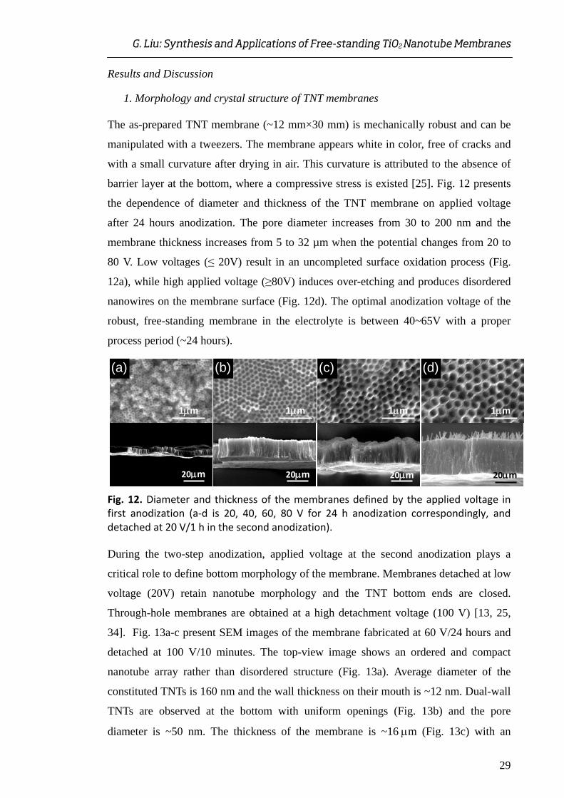
1. Morphology and crystal structure of TNT membranes
The as-prepared TNT membrane (~12 mm×30 mm) is mechanically robust and can be
manipulated with a tweezers. The membrane appears white in color, free of cracks and
with a small curvature after drying in air. This curvature is attributed to the absence of
barrier layer at the bottom, where a compressive stress is existed [25]. Fig. 12 presents
the dependence of diameter and thickness of the TNT membrane on applied voltage
after 24 hours anodization. The pore diameter increases from 30 to 200 nm and the
membrane thickness increases from 5 to 32 µm when the potential changes from 20 to
80 V. Low voltages (≤ 20V) result in an uncompleted surface oxidation process (Fig.
12a), while high applied voltage (≥80V) induces over-etching and produces disordered
nanowires on the membrane surface (Fig. 12d). The optimal anodization voltage of the
robust, free-standing membrane in the electrolyte is between 40~65V with a proper
process period (~24 hours).
Fig. 12. Diameter and thickness of the membranes defined by the applied voltage in first anodization (a‐d is 20, 40, 60, 80 V for 24 h anodization correspondingly, and detached at 20 V/1 h in the second anodization).
During the two-step anodization, applied voltage at the second anodization plays a
critical role to define bottom morphology of the membrane. Membranes detached at low
voltage (20V) retain nanotube morphology and the TNT bottom ends are closed.
Through-hole membranes are obtained at a high detachment voltage (100 V) [13, 25,
34]. Fig. 13a-c present SEM images of the membrane fabricated at 60 V/24 hours and
detached at 100 V/10 minutes. The top-view image shows an ordered and compact
nanotube array rather than disordered structure (Fig. 13a). Average diameter of the
constituted TNTs is 160 nm and the wall thickness on their mouth is ~12 nm. Dual-wall
TNTs are observed at the bottom with uniform openings (Fig. 13b) and the pore
diameter is ~50 nm. The thickness of the membrane is ~16m (Fig. 13c) with an
20m 20m 20m 20m
(a) (b) (c) (d)
1m 1m 1m 1m

G. Liu: Synthesis and Applications of Free-standing TiO2 Nanotube Membranes
30
estimated aspect ratio of 100 (length/diameter). This vertically oriented, close-packed
TNTs go straightly from the top to bottom which is important to supply a direct pathway
for electron transportation in the nanostructure.
2 (Cu K)10 20 30 40 50 60 70 80
Inte
nsity
(a.
u.)
(101
)
(204
)
(211
)(1
05)
(200
)
(004
)
(220
)
(103
)(1
12)
(107
)
Fig. 13. SEM images of the TNT membrane (a) Top view. (b) Bottom view. (c) Cross‐sectional view. TEM images of (d) single amorphous TNT and (e) crystalline TNTs. (f) TEM image shows crystalline order. (g) and (h) are selected area electron diffraction (SAED) pattern for the amorphous and the crystalline TNT. i) XRD patterns of the membrane.
Inspection of the as-prepared amorphous TNTs by using high resolution TEM (Fig. 13d
and g) shows a disordered lattice characteristic. A large number of localized states in the
amorphous structure act as traps and recombination centers, which degrades the TNT
photo-catalytic/electronic performance [56, 78, 82, 83]. Crystallized and ordered
structure is instantly apparent after annealing (Fig. 13e and f). The crystal lattice fringe
spacing is 0.35nm corresponding to the spacing of (101) lattice plane of the anatase
TiO2 [71]. Selected area electron diffraction (SAED) pattern taken from a randomly
chosen nanotube displays diffused rings (Fig. 13h). These rings indicate that the TNT
membrane is polycrystalline. Meanwhile, XRD pattern (Fig. 13i) shows three strong
diffraction peaks corresponding to the three isolated rings. All diffraction fringes are
(a)
16m
(b) (c)
20m 500nm 500nm
(e) (f)(d)
(g) (h) (i)
G. Liu: Synthesis and Applications of Free-standing TiO2 Nanotube Membranes
31
indexed as the anatase TiO2 phase (JCPDS file 84-1286), the diffraction peaks at
2θ=25.5°, 38.1°, 48.3° are identified to be (101), (004), (200) crystal faces, respectively.
The grain diameter estimated from TEM analysis is 80 nm while Scherrer analysis of
the X-ray patterns gives a value of 82 nm from the (101) diffraction peak. The as-
prepared amorphous TNTs crystallize initially as small grains, and then coalesce to form
larger crystallites as the increasing of temperature [71]. However, the grain is not
uniformly crystallized in TNTs, while the large size grains are formed on the location of
thick wall with high local temperature [71, 83].
2. Photoelectrical measurement
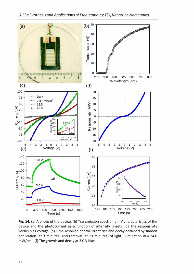
Fig. 14a is a photograph of the packaged photoelectrical device for photoconductive
characterization of the membranes, where Au electrodes on the silicon substrates are
observed through the semi-transparency membrane (the sample in Fig. 13).
Transmission spectrum of the free-standing TNT membrane was recorded between light
wavelength 200-800 nm before assembly (Fig. 14b). It can be seen that the light is
completely absorbed by the TNT membrane in the UV region below 330 nm
(transmittance ~ 0%). In contrast, the transmittance reaches a value over 40% at
wavelengths greater than 550 nm. It indicates that the membrane ensures selective
absorption of UV light (< 330 nm) [3, 84].
Fig. 14c shows I-V characteristics of the TNT membrane device in dark and under UV
illumination by a 320 nm light source at various intensities (5 minutes measurement for
each case). The packaged photoelectrical device exhibits a nonlinear I-V curve due to
the metal-semiconductor-metal structure [85, 86]. The near symmetric I-V curves
indicate that there are two back-to-back contacts on the TNT membrane. At a fixed bias
of 3.0 V, the photocurrents are about 11, 20 and 49 times larger than the dark current
(1.8 A) value when the system is illuminated by the UV light with intensity of 2.8
(20.5 A), 12.5 (38.2 A) and 42.0 (91.5 A) mW/cm2 respectively. The dependence of
photocurrent on light intensity is plotted in the inset of Fig. 14c. The increases of photon
induced current with increasing light intensity is arisen from the electron-hole pairs
excited by the incident light which has an energy larger than the band gap [8, 86, 87]. It
is consistent with the fact that the charge carrier photogeneration efficiency is
proportional to the absorbed photon flux. The light power dependence is further fitted to
a power law, Ip~θ, where θ determines the response of the photocurrent to light
G. Liu: Synthesis and Applications of Free-standing TiO2 Nanotube Membranes
32
Wavelength (nm)200 300 400 500 600 700 800
Tra
nsm
issi
on (
%)
0
10
20
30
40
50
Voltage (V)-5 -4 -3 -2 -1 0 1 2 3 4 5
Cur
ren
t (
A)
-100
-75
-50
-25
0
25
50
75
100
Dark2.8 mW/cm2
12.542.0
(mW/cm2)0 15 30 45
Cu
rre
nt
(A
)
0
50
100
150
200
1.0 V
3.0 V
5.0 V
Voltage (V)-5 -4 -3 -2 -1 0 1 2 3 4 5
Res
pons
ivity
(A
/W)
-20
-15
-10
-5
0
5
10
15
20
Time (s)0 300 600 900 1200 1500 1800
Cur
rent
( A
)
0
20
40
60
80
100
120
140
1.0 V
3.0 V
5.0 V
On Off
Time (s)175 180 185 190 195 200 205 210
Cu
rren
t ( A
)
20
24
28
32
36
40
Time (s)780 790 800 810
Cur
rent
(A
)
48
50
52
54
Fig. 14. (a) A photo of the device. (b) Transmission spectra. (c) I‐V characteristics of the device and the photocurrent as a function of intensity (inset). (d) The responsivity versus bias voltage. (e) Time‐resolved photocurrent rise and decay obtained by sudden
application (at 3 minutes) and removal (at 13 minutes) of light illumination = 24.0 mW/cm2. (f) The growth and decay at 3.0 V bias.
(c) (d)
(e) (f)
(a) (b)

G. Liu: Synthesis and Applications of Free-standing TiO2 Nanotube Membranes
33
intensity. The fitting gives a nearly linear behavior with θ = 0.65 at bias 3.0 V. This non-
unity (0.5<θ<1) exponent suggests a complex process of electron-hole generation,
recombination, and trapping within the membrane [88]. Fig. 14d displays the
responsivity Rλ=ΔI/(S) versus applied-voltage under =12.5 mW/cm2. ΔI is the
difference between the current under illumination and the dark current, S is the area of
membrane, λ is the wavelength of irradiated light [89]. The spectral response at 320 nm
is ~30 A/W under 5.0V bias, corresponding to external quantum efficiency (QE=hcRλ/eλ)
~10695%. In comparing with monolayer or nanosheets [87, 90], dense nanoparticulates
/crystals devices [91-93] whose photocurrents are normally below 10 A, our device
provides a higher photocurrent ~200 A at bias voltage of 5.0 V.
Fig. 14e shows photocurrent response during a 10-minute illumination pulse under
biases of 1.0, 3.0 and 5.0 V. It is evident that applied bias voltage influences on/off ratio
of the devices [94, 95]. At each bias, the initial current rises within 2 s under
illumination as shown in Fig. 14f. The photocurrent rise is then followed by a slower
component [96], in which the photocurrent increases in about 10 minutes before
saturating. We observed plural time constants of the responsivity since the photocurrent
response process generates a number of different classes of trap-states with different
lifetimes [93]. The photocurrent decay starts with a fast component, during which the
photocurrent is reduced in the first 2-10 s after turning off the excitation (inset of Fig.
14f). This fast decay process follows a first-order exponential relaxation function [96].
A further slow decay process lasts about tens of minutes before returning back to its
initial dark-state.

G. Liu: Synthesis and Applications of Free-standing TiO2 Nanotube Membranes
34
Time (ks)0 1 2 3 4 5 6
Cu
rren
t (
A)
20
25
30
35
40
45
50
55
Time (ks)0.0 0.8 1.6 2.4 3.2 4.0 4.8
Cu
rren
t (
A)
5
10
15
20
25
Time (ks)0.0 0.8 1.6 2.4 3.2 4.0 4.8
Cur
rent
( A
)
0
4
8
12
16
20
(a)
(b)
(c)
Fig. 15. Time‐dependent photoresponse under pulse illumination (a) at 24.0 mW/cm2 with 5 minnutes duration, (b) at different light intensities (5.0, 6.0, 7.0, 8.0, 9.0 mW/cm2) with 5 minutes duration, (c) at 4.0 mW/cm2 with various durations (1, 3, 5, 7, 9 minutes).
Fig. 15 shows reproducibility and stability of the TNT membranes under the bias of 3.0
V during repetitive switching of light illumination. The photocurrent increases to a
value of 53 μA and then decreases to its initial level (Fig. 15a). After a given number of
cycles, the photocurrent remains consistent, stable and reproducible. The origins of the
observed current fluctuations are surface species absorption/desorption or appearance of
defects [85]. The membrane response during tiny changes of light intensity and duration
are depicted in Fig. 15b and c. The photocurrent increases with increasing intensity
from 5.0 to 9.0 mW/cm2 as well as extending duration from 1 to 9 minutes at 4.0
mW/cm2. This increase is consistent with an increase of electron lifetime due to a
reduction in the oxygen readsorption rate. It can be understood that the photocurrent
gain depends on both the UV light intensity and duration, and the gain is accompanied
by a slow decay [97].

G. Liu: Synthesis and Applications of Free-standing TiO2 Nanotube Membranes
35
3. Inherent physical mechanism
The optoelectronic measurements provide insight of charge transport in TNT
membranes, including charge injection from gold contacts to the membrane and charge
transport in the three dimensional TNT arrays [91, 97]. It is generally accepted that
oxygen molecules are adsorbed onto the TNT surfaces by capturing free electrons from
the semiconductor [O2(g)+e-→O2-(ad)] (Fig. 16a), which creates a low-conductivity
depletion layer near the surface [8, 84, 91, 98]. Upon UV excitation, electron-hole pairs
are generated. The holes migrated to the surface along the potential gradient produced
by band-bending either discharge the negatively charged adsorbed oxygen ions [h++O2-
→O2(g)] to photodesorb oxygen from the surfaces or get trapped at the TNT surfaces.
This leads to an enhancement of carrier injection and transport, producing a persistent
photocurrent [8, 95]. We note that the photocurrent response in our devices is larger
Fig. 16. Schematic illustration of (a) Oxygen adsorption in the dark and desorption under UV illumination. (b) The NT‐NT junction barrier for electron transfer in the matrix, showing a decrease in NT‐NT junction barrier height from the light‐off state to light‐on state.
(three orders) than the individual nanostructure-based devices whose photocurrent is in
the range of several pA to nA [8, 86, 99]. As comparing with the immobilized
membrane on Ti substrates, the absence of blocking layer on the membrane ensuring

G. Liu: Synthesis and Applications of Free-standing TiO2 Nanotube Membranes
36
perfect crystallinity and the large surface-to-volume ratio of the TNT increase the
number of surface trap states, and facilitate oxygen adsorption / desorption at the
surface. Compared to nanogranular films, oriented polycrystalline TNTs offer the
advantage of directed electron transport, and are expected to have higher electron
mobility. However, our data is inconsistent with this result. We assume that the slow
photoresponse rise-drop speeds are caused by a single sharp resonance arising from
exciton-like trap states [100]. Long spacing between electrodes in the devices extends
the transport path of electrons and increases intercrystalline contacts, which also reduces
the electron mobility [89, 101, 102]. Nevertheless, the device shows a high sensitivity to
the UV light due to the existence of a percolated matrix. The electron conduction in the
matrix is dominated by a combination of the grain-boundary barriers inside single
nanotube and the junction barriers between neighboring tubes (NT-NT junction barriers)
[86, 98]. Upon illumination, the carrier density in TNTs would narrow the barrier width
or lower the effective barrier height (Fig. 16b), which facilitates an increase in electron
transportation and results in an increase in conductivity of the TNT network [91, 98].
Since the light-induced barrier height modulation is much faster than the oxygen-
diffusion, therefore the time response speed of the device is much fast in the first few
seconds [71, 78, 96].
2.3.2 Small diameter TiO2 nanotubes with enhanced photoresponsivity (Article V)
We report ultraviolet (UV) light detection of thin wall TiO2 nanotubes (TNTs) with open
diameter ~20 nm obtained by a two anodization procedure. This small diameter
nanotubular geometry shows significant enhancement of the photoresponsivity and
results in a large increase of photocurrent. The photocurrent is one order higher than that
of classical nanotubes with diameter of 140 nm at -1.0 V bias. We attribute this
improvement to the modulation of hole carrier density as a result of field effects from
the diameter-dependent population of the surface-trapped electrons. This finding
demonstrates inherent size effects of internal gain in semiconductor nanotubes.
Experimental details
The anodization was carried out in a two-electrode system. The setup details are
described in reference [25]. For the growth of small diameter TNTs, a facile process was
introduced (Fig. 17). First anodization was started with growth of TNTs on Ti foil ~60
V/24 h (Fig. 17 (1)), followed by annealing to crystallize the TNTs (Fig. 17 (2)). Then,
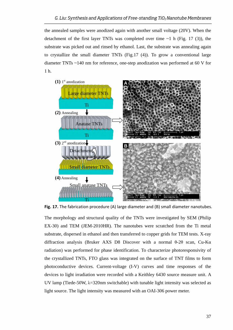
G. Liu: Synthesis and Applications of Free-standing TiO2 Nanotube Membranes
37
the annealed samples were anodized again with another small voltage (20V). When the
detachment of the first layer TNTs was completed over time ~1 h (Fig. 17 (3)), the
substrate was picked out and rinsed by ethanol. Last, the substrate was annealing again
to crystallize the small diameter TNTs (Fig.17 (4)). To grow a conventional large
diameter TNTs ~140 nm for reference, one-step anodization was performed at 60 V for
1 h.
(1) 1st anodization
(2) Annealing
(3) 2nd anodization
(4) Annealing
Fig. 17. The fabrication procedure (A) large diameter and (B) small diameter nanotubes.
The morphology and structural quality of the TNTs were investigated by SEM (Philip
EX-30) and TEM (JEM-2010HR). The nanotubes were scratched from the Ti metal
substrate, dispersed in ethanol and then transferred to copper grids for TEM tests. X-ray
diffraction analysis (Bruker AXS D8 Discover with a normal θ-2θ scan, Cu-Kα
radiation) was performed for phase identification. To characterize photoresponsivity of
the crystallized TNTs, FTO glass was integrated on the surface of TNT films to form
photoconductive devices. Current-voltage (I-V) curves and time responses of the
devices to light irradiation were recorded with a Keithley 6430 source measure unit. A
UV lamp (Tiede-50W, λ=320nm switchable) with tunable light intensity was selected as
light source. The light intensity was measured with an OAI-306 power meter.
Detachment
A
Large diameter TNTs
B
Small diameter TNTs
Ti
Ti
Anatase TNTs
Small anatase TNTs
Ti
G. Liu: Synthesis and Applications of Free-standing TiO2 Nanotube Membranes
38
Results and discussion
Fig. 17-A shows a top-view SEM image of the large diameter TNTs grown at 60 V for
1h. It is evident that the ordered nanotube array consists of well-aligned nanotubes with
an average inner diameter of 140 nm and wall thickness ~15 nm. The image of small
diameter TNTs fabricated by the two anodization step, as shown Fig. 17-B, indicates
that the TNTs remain compact and no destructive changes after detaching the first
crystalline layer. The constituted TNTs are of an average diameter of 20 nm with a thin
wall ~ 5 nm. During second anodic step, the first crystalline TNT layer serves as a
buffer for reducing the strength of electrical field and to protect the new formed
nanotubes from chemical dissolution. Thus, uniform and small diameter nanotubes are
realized after the second anodization at 20 V for 1 hour [103]. These close-packed,
small diameter nanotube arrays provide a direct pathway for electron transport at the
nanotube walls. Minor bottom parts of the first tube layer left on the small diameter
tubes, which serves as the electron transporter for effective charge separation and rapid
transport of the photogenerated electrons [104].
As the annealing temperature increases from room temperature to 800 OC, the phase of
as-prepared TNTs is changed as amorphous→ anatase → rutile. The TNT morphology
is collapsed at temperature above 600 OC. To form anatase TNT with preferred
morphology and higher photoelectric activity, annealing at 350~500 OC for 2-3 h in
oxygen ambient is a reasonable temperature process [8, 25, 78, 105]. The TEM image
and selected-area electron diffraction (SAED) pattern of the TNTs are shown in Fig. 18.
The high resolution TEM image shows a disordered characteristic for as-prepared
amorphous TNTs (Fig. 18(a)). Crystallized and ordered structures of the nanotubes are
observed after annealing at 500 OC for 3 h (Fig. 18(b)). The image reveals distinctive
lattice fringes spaced by 0.35 nm and exhibits anatase-type polycrystalline Debye-
Scherrer rings in the upper-right inset. XRD pattern (Fig. 18(c)) further confirms that
the as-prepared TNT is amorphous and only diffraction peaks of Ti substrate are
detected (JCPDS file 44-1294). On the contrary, the crystallized counterpart shows three
strong diffraction peaks corresponding to the three isolated rings. All reflections are
indexed (JCPDS file 84-1286), and the diffraction peaks at 2θ=25.5°, 38.1°, 48.3° are
identified to be the (101), (004), (200) crystal faces respectively. There is no significant
change in the pore diameter or wall thickness after annealing.

G. Liu: Synthesis and Applications of Free-standing TiO2 Nanotube Membranes
39
2 (degree)10 20 30 40 50 60 70 80
Inte
nsi
ty (
a.u
.)
(101
)
(204
)
(21
1)(1
05)(200
)
(004
)
(21
5)
(22
0)(1
16)
Ti
Anatase
Amorphous Ti
Ti
TiTi
Ti
(c)
Fig. 18. TEM characterizations of (a) amorphous and (b) anatase TNTs (c) XRD patterns.
To extract the size-dependent photoelectrical properties of the crystallized TNTs, a
FTO/TNT/Ti photoconductive device is then assembled, as schematically shown in the inset
of Fig. 19(a). Two sets of linear sweep voltammograms are recorded in Fig. 19(a) under
both dark and UV illumination of 5 mW/cm2. I-V curves present linear dependence with the
applied bias at forward region while it exhibits a nonlinear behavior with the reverse bias.
In particular, with the reverse bias, the FTO/TNT/Ti heterojunction gives a better
photoresponsivity with large ratios (Iphoto/Idark) approximately 735 (Sample B) and 27
(Sample A) at -1.0 V. We assume that the photoresponse is likely to be dominated by the
Ti/TiO2 heterojunction area. Both samples show small dark current on the order of ~ 10 A.
The sample A keeps a larger dark current with the reverse bias, indicating the background
current of devices is relevance to the sign and intensity of the external electric field. The
device of the small diameter nanotubes not only shows pronounced photoresponse under
light illumination, but also exhibits even higher photocurrent. The maximum photocurrent is
7.5A at 0.2 V, which is about 6 times larger than that ~1.2A for sample A. Similar
enhancement of photoresponsivity is observed with a small reverse bias -0.1 V (Fig. 19(b)).
This confirms a better interfacial charge transfer occurred in small diameter TNTs. Fig. 19(c)
(a) (b)
5 nm 5 nm
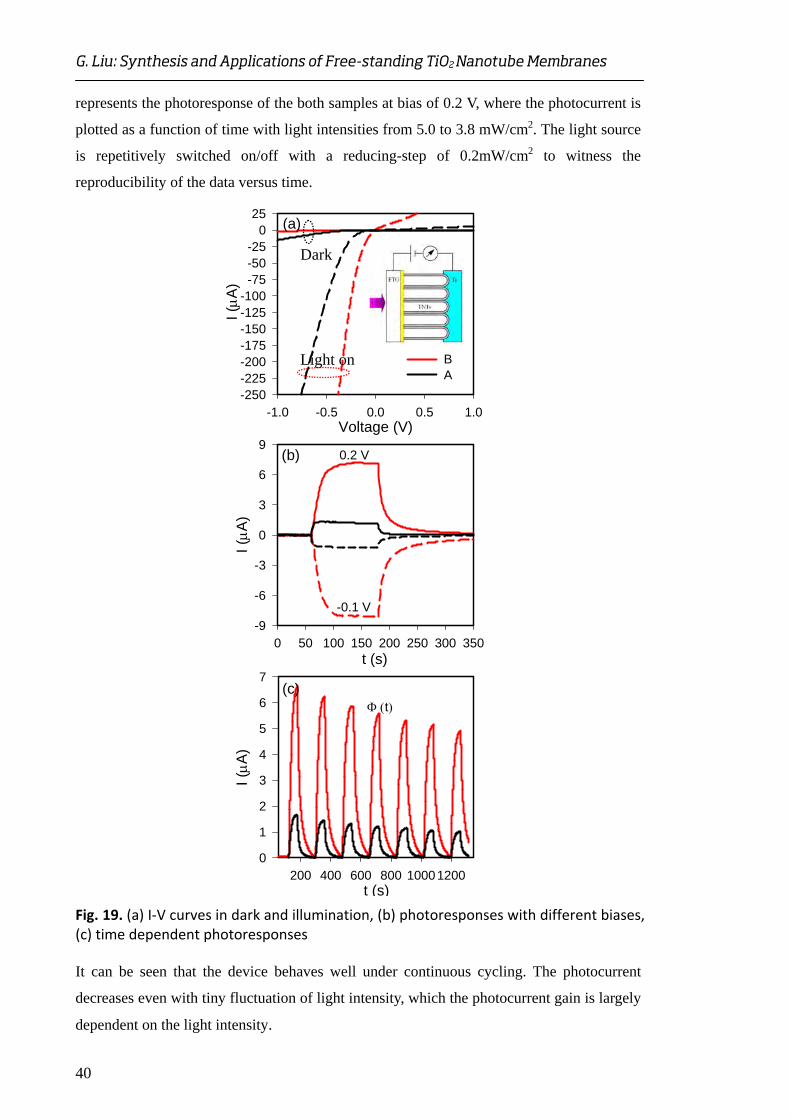
G. Liu: Synthesis and Applications of Free-standing TiO2 Nanotube Membranes
40
represents the photoresponse of the both samples at bias of 0.2 V, where the photocurrent is
plotted as a function of time with light intensities from 5.0 to 3.8 mW/cm2. The light source
is repetitively switched on/off with a reducing-step of 0.2mW/cm2 to witness the
reproducibility of the data versus time.
t (s)0 50 100 150 200 250 300 350
I (
A)
-9
-6
-3
0
3
6
9Voltage (V)
-1.0 -0.5 0.0 0.5 1.0
I (
A)
-250-225-200-175-150-125-100
-75-50-25
025
BA
0.2 V
-0.1 V
(a)
(b)
t (s)200 400 600 800 10001200
I (
A)
0
1
2
3
4
5
6
7
t(c)
Fig. 19. (a) I‐V curves in dark and illumination, (b) photoresponses with different biases, (c) time dependent photoresponses
It can be seen that the device behaves well under continuous cycling. The photocurrent
decreases even with tiny fluctuation of light intensity, which the photocurrent gain is largely
dependent on the light intensity.
Dark
Light on

G. Liu: Synthesis and Applications of Free-standing TiO2 Nanotube Membranes
41
The irradiation induced conductivity Δσ (photoconductivity) occur either due to a
change in the carrier concentration Δn (carrier photogeneration) or to a change in the
carrier mobility Δμ [51, 52, 106, 107]. Δn >> Δμ and the time dependence of the
mobility is negligible. The photocurrent reduces to the usual form
( )photo photo effI EA e n d EA , where e is the electronic charge, d is the nanotube
diameter, E is the applied electric field and A is the area. The field effect from the
trapped holes at the TNT surfaces is diameter-dependent. The effective carrier density
modulation can be expressed as ( ) ( )eff accn d n n d [51, 52, 100]. The number of the
electron-hole pairs created at a tube cross section per unit length is proportional to 2 2( ) / 4o id d , the number of surface trapped holes per unit length is proportional to
( )o id d , where do and di is outer and inner wall diameter of TNT respectively.
Provided that the induced electron concentration is directly proportional to the number
of surface-trapped holes by an electrostatic interaction, the accumulated hole
concentration is expressed by2 2
4 ( ) 1 1
( )o i
acco i o i
d dn
d d d d
, is the wall thickness
[51, 52]. It means that the accumulated hole concentration is inversely proportional to
the wall thickness. So we should obtain ~ 3 times difference in Δnacc between the two
nanotubes, which is qualitatively consistent with the variation of the observed
photocurrent (see Fig.19 (b)-(c)). In this experiment, the thickness of large and small
diameter tubes (evaluated from the growth rate at 60 and 20V) is ~ 680 and 200 nm,
respectively. Long tube length extends the transport path of electrons and increases
intercrystalline contacts, which decreases the electron mobility [4, 108]. The decrease in
diameter and wall thickness of nanotubes enhances the specific surface area, so that the
dissociation efficiency of excitons and the accumulated electron concentration increases
[51, 54, 109]. Therefore, the large specific surface area and a fast transport path for
carriers are the main advantages of small diameter nanotubes as compared to large ones.
The field effect from the diameter-dependent population facilitates an increase in
electron transportation and results in a significant increase of photoresponsivity in the
small diameter TNTs.


G. Liu: Synthesis and Applications of Free-standing TiO2 Nanotube Membranes
43
3 Conclusions
This thesis aims to develop cutting-edge technology for reliable fabrication of TNT
membranes. Materials formation mechanisms and their photoconductive properties have
been investigated systematically. The main conclusions are drawn in the following
aspects:
A simple process was developed for fabricating amorphous TNT membranes. The
anodization voltage is critical for the detachment through regulating the migration
of fluoride ions on the barrier. Rinsing the as-prepared TNT membranes by pure
ethanol prevents morphological disorder induced by capillary stress and results in a
clean surface with ordered nanostructure. Reducing the rate of ethanol evaporation
by covering an additional cleanroom paper on the as-anodized substrates is a key
step to prepare a large scale and flat surface TNT membranes.
A voltage-dependent investigation was performed for the detachment process of
free-standing crystalline TNT membranes. Crystallized TNT membranes with high
ordered nanotubes were effectively detached from the substrate by taking
advantage of different mechanical stability between the layers. The membrane
detached at low voltage preserves its nanotube morphology and the bottom of tubes
are closed, while through-hole membrane with fast detachment can be obtained at a
high detachment voltage.
TNT membranes were synthesized by a two-step anodic procedure, in which
dependence of the TNT morphology on the applied voltage is experimentally
present. Due to the large surface area-to-volume ratio and high quality crystal
structure, the membrane exhibits a sensitive spectral response to the ultra violet
(UV) light. The photoresponse origins from internal gain induced by desorption of
oxygen molecules from the nanotube surfaces and reduction of the barrier at
neighboring tubes under UV illumination.

G. Liu: Synthesis and Applications of Free-standing TiO2 Nanotube Membranes
44
We compare the UV light sensitivity between the small diameter ~20 nm and the
conventional diameter TNTs. The small diameter nanotube device enhances the UV
photoresponsivity and leads to a larger increase of photocurrent. The photocurrent
value increases ~3 orders of magnitude when the light switches from off to on
status. These observations is associated with the modulation of hole carrier density,
which comes from field effects of the diameter-dependent population of the
electrons.
This work provides powerful approach to tailor the properties of self-organized TNTs,
which may have far-reaching implications in the design of future nanoscale systems.
The progress together with emerging methods for deterministic assembly, leads to
compelling opportunities for research from basic studies of two-dimensional physics to
the development of applications such as optoelectronic or photovoltaic devices,
photocatalysis, nano-template and sensors etc.

G. Liu: Synthesis and Applications of Free-standing TiO2 Nanotube Membranes
45
References
[1] K. Shankar, J. I. Basham, N. K. Allam, et al., Recent advances in the use of TiO2
nanotube and nanowire arrays for oxidative photoelectrochemistry, J. Phys. Chem.
C 2009, 113, 6327-6359.
[2] G. K. Mor, K. Shankar, M. Paulose, O.K. Varghese, C.A. Grimes, Enhanced
photocleavage of water using titania nanotube arrays, Nano Lett. 5 (2005) 191-195.
[3] G. K. Mor, O. K. Varghese, M. Paulose, K.Shankar, C.A. Grimes, A review on
highly ordered, vertically oriented TiO2 nanotube arrays: Fabrication, material
properties, and solar energy applications, Sol. Energy Mater. Sol. Cells. 90 (2006)
2011-2075.
[4] P. Roy, D. Kim, K. Lee, E. Spiecker, TiO2 nanotubes and their application in dye-
sensitized solar cells, P. Schmuki, Nanoscale 2 (2010) 45-59.
[5] S. Devipriya, S. Yesodharan, Photocatalytic degradation of pesticide contaminants
in water, Sol. Energy Mater. Sol. Cells 86 (2005) 309-348.
[6] U.I. Gaya, A.H. Abdullah, Heterogeneous photocatalytic degradation of organic
contaminants over titanium dioxide: A review of fundamentals, progress and
problems, J. Photochem. Photobiol. C 9 (2008) 1-12.
[7] M. Paulose, O. K. Varghese, G. K. Mor, C.A. Grimes, K. G. Ong, Unprecedented
ultra-high hydrogen gas sensitivity in undoped titania nanotubes, Nanotechnology
17 (2006) 398-402.
[8] J. Zou, Q. Zhang, K. Huang, N. Marzari, Ultraviolet photodetectors based on anodic
TiO2 nanotube arrays, J. Phys. Chem. C, 114(2010)10725-10729.
[9] P. Roy, S. Berger, and P. Schmuki, TiO2 Nanotubes: Synthesis and Applications,
Angew. Chem. Int. Ed. 50 (2011) 2904-2939.
[10] C. A. Grimes, G. K. Mor, TiO2 nanotube arrays synthesis, properties, and
applications, Springer, New York, 2009, ISBN 978-1-4419-0067-8.
[11] D. Gong, C. A. Grimes, O. K. Varghese, Titanium oxide nanotube arrays
prepared by anodic oxidation, J. Mater. Res., 16 (2001)3331-3334.
G. Liu: Synthesis and Applications of Free-standing TiO2 Nanotube Membranes
46
[12] M. Paulose, H. E. Prakasam, O. K. Varghese, L. Peng, K. C. Popat, G. K. Mor,
T.A. Desai, C. A. Grimes, TiO2 nanotube arrays of 1000�m length by anodization
of titanium foil: phenol red diffusion, J. Phys. Chem. C. 111 (2007) 14992-14997.
[13] G. Liu, K. Wang, N. Hoivik, H. Jakobsen, Progress on free-standing and flow-
through TiO2 nanotube membranes, Sol. Energy Mater. Sol. Cells. 98 (2012) 24-38.
[14] B.X. Lei, J.Y. Liao, R. Zhang, J. Wang, C.Y. Su, D.B. Kuang, Ordered
crystalline TiO2 nanotube arrays on transparent FTO glass for efficient dye-
sensitized solar cells, J. Phys. Chem. C. 114 (2010) 15228-15233.
[15] Q. Zheng, H. Kang, J. Yun, J. Lee, J.H. Park, S. Baik, Hierarchical construction
of self-standing anodized titania nanotube arrays and nanoparticles for efficient and
cost-effective front-illuminated dyesensitized solar cells, ACS Nano 5 (2011) 5088-
5093.
[16] C.J. Lin, W.Y. Yu, Y.T. Lu, S.H. Chien, Fabrication of open-ended high aspect-
ratio anodic TiO2 nanotube films for photocatalytic and photoelectrocatalytic
applications, Chem. Commun. (2008) 6031- 6033.
[17] Q.W. Chen, D.S. Xu, Z.Y. Wu, Z.F. Liu, Free-standing TiO2 nanotube arrays
made by anodic oxidation and ultrasonic splitting, Nanotechnology 19 (2008)
365708 (5pp).
[18] O.K. Varghese, M. Paulose, T.J. LaTempa, C. A. Grimes, High-rate solar
photocatalytic conversion of CO2 and water vapor to hydrocarbon fuels, Nano Lett.
9 (2009) 731-737.
[19] K. Yu , W. Yu, M. Kuo, Y. Liou, S. Chien, Pt/titania-nanotube: A potential
catalyst for CO2 adsorption and hydrogenation, Appl. Catal. B: Environ. 84 (2008)
112-118.
[20] S.P. Albu, A. Ghicov, J.M. Macak, R. Hahn, P. Schmuki, Self-Organized, free-
standing TiO2 nanotube membrane for flow-through photocatalytic applications,
Nano Lett. 7 (2007) 1286-1289.
[21] B. Zhu, J.J. Li, Q.W. Chen, R.G. Cao, J.M. Li, D.S. Xu, Artificial, switchable
K+-gated ion channels based on flow-through titania-nanotube arrays, Phys. Chem.
Chem. Phys. 12 (2010) 9989-9992.
[22] J. Lin, J.F. Chen, X.F. Chen, Facile fabrication of free-standing TiO2 nanotube
membranes with both ends open via self-detaching anodization, Electrochem.
Commun. 12 (2010) 1062-1065.

G. Liu: Synthesis and Applications of Free-standing TiO2 Nanotube Membranes
47
[23] K. Kant, D. Losic, A simple approach for synthesis of TiO2 nanotubes with
through-hole morphology, Phys. Status Solidi RRL. 3 (2009) 139-141.
[24] S. Banerjee, M. Misra, S. K. Mohapatra, C. Howard, S.K. Mohapatra and S. K.
Kamilla, Formation of chelating agent driven anodized TiO2 nanotubular membrane
and its photovoltaic application, Nanotechnology 21 (2010) 145201(9pp).
[25] G.H. Liu, N. Hoivik, K.Y. Wang, H. Jakobsen, A voltage-dependent
investigation on detachment process for free-standing crystalline TiO2 nanotube
membranes, J. Mater. Sci. 46 (2011) 7931-7935.
[26] V. K. Khanna, Adhesion-delamination phenomena at the surfaces and interfaces
in microelectronics and MEMS structures and packaged devices, J. Phys. D: Appl.
Phys. 44 (2011) 034004 (19pp).
[27] J.W. Ng, X.W. Zhang, T. Zhang, Construction of self-organized free-standing
TiO2 nanotube arrays for effective disinfection of drinking water, J Chem. Technol.
Biotechnol. 85 (2010) 1061-1066.
[28] J. Wang, Z. Lin, Freestanding TiO2 nanotube arrays with ultrahigh aspect ratio
via electrochemical anodization, Chem. Mater. 20 (2008) 1257-1261.
[29] X. Meng, T.Y. Lee, H. Chen, D.W. Shin, K.W. Kwon, S.J. Kwon, J.B. Yoo,
Fabrication of free standing anodic titanium oxide membranes with clean surface
using recycling process, J. Nanosci. Nanotechno. 10 (2010) 4259-4265.
[30] D. Fang, K.L. Huang, S.Q. Liu, Z.P. Luo, X.X. Qing, Q.G. Zhang, High-density
NiTiO3/TiO2 nanotubes synthesized through sol-gel method using well-ordered TiO2
membranes as template, J. Alloys Compd. 498 (2010) 37-41.
[31] D. Fang, K.L. Huang, S.Q. Liu, D.Y. Qin, High density copper nanowire arrays
deposition inside ordered titania pores by electrodeposition, Electrochem. Commun.
11 (2009) 901-904.
[32] Y. Shin, S. Lee, A free standing membrane of highly ordered anodic ZrO2
nanotube arrays, Nanotechnology 20 (2009) 105301(5pp).
[33] S. Singh, M. Festin, W.R.T. Barden, L. Xi, J.T. Francis, P. Kruse, Universal
method for the fabrication of detachable ultrathin films of several transition metal
oxides, ACS Nano. 2 (2008) 2363-2373.
[34] D.A. Wang, L.F. Liu, Continuous fabrication of free-standing TiO2 nanotube
array membranes with controllable morphology for depositing interdigitated
heterojunctions, Chem. Mater. 22(2010) 6656-6664.

G. Liu: Synthesis and Applications of Free-standing TiO2 Nanotube Membranes
48
[35] Y. Jo, Jung I, I. Lee, J. Choi, Y. Tak, Fabrication of through-hole TiO2 nanotubes
by potential shock, Electrochem. Commun. 12 (2010) 616-619.
[36] S. LI, G. Zhang, One-step realization of open-ended TiO2 nanotube array by
transition of the anodizing voltage, Journal of the Ceramic Society of Japan 118
(2010) 291-294.
[37] Q.W. Chen, D.S. Xu, Large-Scale, noncurling, and free-standing crystallized
TiO2 nanotube arrays for Dye-sensitized solar cells, J. Phys. Chem. C 113 (2009)
6310-6314.
[38] K. Li, Z. Xie, S. Adams, K.Li, Z. Xie, A reliable TiO2 nanotube membrane
transfer method and its application in photovoltaic devices, Electrochimica Acta 62
(2012) 116-123.
[39] S. Yoriya, M. Paulose, O.K. Varghese, G.K. Mor, C.A. Grimes, Fabrication of
vertically oriented TiO2 nanotube arrays using dimethyl sulfoxide electrolytes, J.
Phys. Chem. C. 111 (2007) 13770-13776.
[40] Q.S. Zhong, D.W. Wang, F. Li, G.Q. Lu, H.M. Cheng, Preparation of free-
standing transparent titania nanotube array membranes, Chinese journal of materials
research. 23 (2009) 118-122.
[41] C.J. Lin , Y.H. Yu , Y.H. Liou, Free-standing TiO2 nanotube array films
sensitized with CdS as highly active solar light-driven photocatalysts, Appl. Catal.
B: Environ. 93 (2009) 119-125.
[42] M. Dubey, M. Shrestha, Y. Zhong, D. Galipeau, H. He, TiO2 nanotube
membranes on transparent conducting glass for high efficiency dye-sensitized solar
cells, Nanotechnology 22 (2011) 285201 (9pp).
[43] J.H. Park, T.W. Lee, M.G. Kang, Growth, detachment and transfer of highly-
ordered TiO2 nanotube arrays: use in dye-sensitized solar cells, Chem. Commun.
(2008) 2867-2869.
[44] D.A. Wang, Y. Liu, B. Yu, F. Zhou, W.M. Liu, TiO2 Nanotubes with tunable
morphology, diameter, and length: synthesis and photo-electrical/catalytic
performance, Chem. Mater. 21 (2009) 1198-1206.
[45] D.A. Wang, B.Yu, C.W. Wang, F. Zhou, W.M. Liu, A novel protocol toward
perfect alignment of anodized TiO2 nanotubes, Adv. Mater. 21 (2009) 1964-1967.
[46] S.P. Albu, A. Ghicov, S. Berger, H, Jha, P. Schmuki, TiO2 nanotube layers:
flexible and electrically active flow-through membranes, Electrochem. Commun. 12
(2010) 1352-1355.

G. Liu: Synthesis and Applications of Free-standing TiO2 Nanotube Membranes
49
[47] Z. Zhang, D. Guo, Y. Xing, G. Zhang, Fabrication of open-ended TiO2 nanotube
arrays by anodizing a thermally evaporated Ti/Au bilayer film, Appl. Surf. Sci. 257
(2011) 4139-4143.
[48] L.L. Li, Y.J. Chen, H.P. Wu, N.S. Wang, E.W. Diau, Detachment and transfer of
ordered TiO2 nanotube arrays for front-illuminated dye-sensitized solar cells,
Energy Environ. Sci. 4(2011)3420-3425.
[49] G. Konstantatos, E.H. Sergeant, nanostructured materials for photon detection,
Nat. Nanotechnol. 5 (2010) 391-400.
[50] L. Cao, J. S. White, J. Park, J. A. Schuller, B.M. Clemens, M.L. Brongersma,
Engineering light absorption in semiconductor nanowire devices, Nat. Mater. 8
(2009) 643-647.
[51] C. J. Kim, H. S. Lee, Y. J. Cho, K. Kang, M. H. Jo, Diameter-dependent internal
gain in Ohmic Ge nanowire photodetectors, Nano Lett. 10 (2010) 2043-2048.
[52] Q. Zhang, J. Qi, X. Li, Y. Zhang, Diameter-dependent internal gain in ZnO
micro/nanowires under electron beam irradiation, Nanoscale 3 (2011) 3060-3063.
[53] R. S. Chen, C. A. Chen, H. Y. Tsai, W. C. Wang,Y. S. Huang, Photoconduction
properties in single-crystalline titanium dioxide nanorods with ultrahigh normalized
gain, J. Phys. Chem. C 116 (2012) 4267-4272.
[54] M. Ouyang, R. Bai, L. Yang, Q. Chen, Y. Han, M. Wang, Y. Yang, H. Chen,
High photoconductive vertically oriented TiO2 nanotube arrays and their composites
with copper phthalocyanine, J. Phys. Chem. C 112 (2008) 2343-2348.
[55] H. Xue, X. Kong, Z. Liu, C. Liu, J. Zhou, W. Chen, TiO2 based metal-
semiconductor-metal ultraviolet photodetectors, Appl. Phys. Lett. 90 (2007) 201118.
[56] X. Kong, C. Liu, W. Dong, X. Zhang, C. Tao, L. Shen, J. Zhou, Y. Fei, S. Ruan
Metal-semiconductor-metal TiO2 ultraviolet detectors with Ni Electrodes, Appl.
Phys. Lett. 94 (2009) 123502.
[57] T. Tachikawa, T. Majima, Exploring the spatial distribution and transport
behavior of charge carriers in a single titania nanowire, J. Am. Chem. Soc. 131
(2009) 8485-8495.
[58] C. Fabrega, F. Hernandez-Ramırez, J. D. Prades, R. Jimenez-Dıaz, T. Andreu, J.
R. Morante, On the photoconduction properties of low resistivity TiO2 nanotubes,
Nanotechnology 21 (2010) 445703.

G. Liu: Synthesis and Applications of Free-standing TiO2 Nanotube Membranes
50
[59] R. S. Chen, C. A. Chen, H. Y. Tsai, W. C. Wang, Y. S. Huang, Ultrahigh
efficient single-crystalline TiO2 nanorod photoconductors, Appl. Phys. Lett. 100
(2012) 123108.
[60] Y. Chang, C. Liu, Y. Tseng, C. Chen, C. Chen, H. Cheng, Direct probe of
heterojunction effects upon photoconductive properties of TiO2 nanotubes fabricated
by atomic layer deposition, Nanotechnology 21 (2010) 225602.
[61] Y. Han, C. Fan, G. Wu, H. Chen, M. Wang, Low-temperature solution processed
utraviolet photodetector based on an ordered TiO2 nanorod array_polymer hybrid, J.
Phys. Chem. C 115 (2011) 13438-13445.
[62] K.Zhu, T.B. Vinzant, N. R. Neale, and A.J. Frank, Removing structural disorder
from oriented TiO2 nanotube arrays: Reducing the dimensionality of transport and
recombination in dye-sensitized solar cells, Nano Lett. 7 (2007) 3739-3746.
[63] D. Kim, A. Ghicov, P. Schmuki, TiO2 Nanotube arrays: Elimination of
disordered top layers ("nanograss") for improved photoconversion efficiency in dye-
sensitized solar cells, Electrochem. Commun. 10 (2008) 1835-1838.
[64] G. Ali, S.H. Yoo, J.M. Kum, Y.N. Kim and S.O. Cho, A novel route to large-
scale and robust free-standing TiO2 nanotube membranes based on N2 gas blowing
combined with methanol wetting, Nanotechnology 22 (2011) 245602.
[65] Y. Alivov, M. Pandikunta, S. Nikishin, Z Y Fan, The anodization voltage
influence on the properties of TiO2 nanotubes grown by electrochemical oxidation,
Nanotechnology 20 (2009) 225602 (6pp).
[66] K. Shankar, G.K. Mor, C.A. Grimes, Highly-ordered TiO2 nanotube-arrays up to
220 μm in length: use in water photoelectrolysis and dye-sensitized solar cells,
Nanotechnology 18 (2007) no.065707.
[67] J.M. Macak, H. Hildebrand, U. Marten-Jahns, Mechanistic aspects and growth of
large diameter self-organized TiO2 nanotubes, J. Electroanal. Chem. 621 (2008)
254-266.
[68] H. Yin, H. Liu, W. Z. Shen, The large diameter and fast growth of self-organized
TiO2 nanotube arrays achieved via electrochemical anodization, Nanotechnology 21
(2010) 035601(7pp).
[69] S. Sreekantan, R. Hazan, Z. Lockman, Photoactivity of anatase-rutile TiO2
nanotubes formed by anodization method, Thin solid films, 518 (2009) 16-21.
G. Liu: Synthesis and Applications of Free-standing TiO2 Nanotube Membranes
51
[70] Y.L. Pang, A. Z. Abdullah, S. Bhatia, Effect of annealing temperature on the
characteristics, sonocatalytic activity and reusability of nanotubes TiO2 in the
degradation of Rhodamine B, Appl. Catal. B: Environ. 100 (2010) 393-402.
[71] D. Fang, Z. Luo, K. Huang, D. C. Lagoudas, Effect of heat treatment on
morphology, crystalline structure and photocatalysis properties of TiO2 nanotubes
on Ti substrate and freestanding membrane, Applied Surface Science, 257 (2011)
6451-6461.
[72] D.D. Li, P.C. Chang, C.J. Chien, J.G. Lu, Applications of tunable TiO2
nanotubes as nanotemplate and photovoltaic device, Chem. Mater. 22 (2010) 5707-
5711.
[73] J.M. Macak, S. Albu, D.H. Kim, I. Paramasivam, S. Aldabergerova, P. Schmuki,
Multilayer TiO2-nanotube formation by two-step anodization, Electrochem. Solid-
State Lett. 10 (2007) K28-K31.
[74] K. Yasuda, P. Schmuki, Electrochemical formation of self-organized zirconium
titanate nanotube multilayers,Electrochem. Commun. 9 (2007) 615-619.
[75] B. Chen, K. Lu, Hierarchically Branched titania nanotubes with tailored
diameters and branch numbers, Langmuir, 28 (2012) 2937-2943.
[76] G. Butail, P. G. Ganesan, R. Teki, R. Mahima, N. Ravishankar, D. J. Duquette,
G. Ramanath, Branched titania nanotubes through anodization voltage control, Thin
Solid Films, 520(2011)235-238.
[77] S.P. Albu, D. Kim, P. Schmuki, Growth of Aligned TiO2 Bamboo-type
nanotubes and highly ordered nanolace, Angew. Chem. Int. Ed. 47 (2008) 1916-
1919.
[78] A. Tighineanu, T. Ruff, S. Albu, R. Hahn, P. Schmuki, Conductivity of TiO2
nanotubes: Influence of annealing time and temperature, Chemical Physics Letters
494 (2010) 260-263.
[79] C.T. Yip, H. Huang, L. Zhou, K. Xie, Y. Wang , T. Feng , J. Li, W.Y. Tam,
Direct and seamless coupling of TiO2 nanotube photonic crystal to dye-sensitized
solar cell: A single-step approach, Adv. Mater. 23(2011)5624-5268.
[80] G.K. Mor, K. Shankar, M. Paulose, O.K. Varghese, C.A. Grimes, Use of highly-
ordered TiO2 nanotube arrays in dye-sensitized solar cells, Nano Lett., 6 (2006) 215-
218.
G. Liu: Synthesis and Applications of Free-standing TiO2 Nanotube Membranes
52
[81] O.K. Varghese, M. Paulose, C.A. Grimes, Long vertically aligned titania
nanotubes on transparent conducting oxide for highly efficient solar cells, Nature
nanotechnology 4 (2009) 592-597.
[82] K. Zhu, N.R. Neale, A. F. Halverson, J.Y. Kim, A.J. Frank, Effects of annealing
temperature on the charge-collection and light-harvesting properties of TiO2
nanotube-based dye-sensitized solar cells, J. Phys. Chem. C 114(2010)13433-13441.
[83] J. Yu, G. Dai, B. Cheng, Effect of crystallization methods on morphology and
photocatalytic activity of anodized TiO2 nanotube array films, J. Phys. Chem. C,
114(2010)19378-19385.
[84] Z. Liu, J. Chen, Y. Zhang, L. Wu, X. Li, The effect of sandwiched Ag in the wall
of TiO2 nanotube on the photo-catalytic Performance, Materials Chemistry and
Physics 128 (2011) 1-5.
[85] X. Fang, Y. Bando, M. Liao, U.K. Gautam, C. Zhi, B. Dierre, B. Liu, T. Zhai, T.
Sekiguchi, Y. Koide, D. Golberg, Single-crystalline ZnS nanobelts as ultraviolet-
light sensors, Adv. Mater. 21 (2009) 2034-2039.
[86] L. Hu, L.Wu, M. Liao, X. Fang, High-performance NiCo2O4 nanofilm
photodetectors fabricated by an interfacial self-assembly strategy, Adv. Mater. 23
(2011) 1988-1992.
[87] H. Yan , Z. Yu , K. Lu , Y. Zhang , Z. Wei, Self-assembly of graphenelike ZnO
superstructured nanosheets and their application in hybrid photoconductors, Small 7
(2011) 3472-3478.
[88] J.S. Jie, W.J. Zhang, Y. Jiang, X.M. Meng, Y.Q. Li, S.T. Lee, Photoconductive
characteristics of single-crystal CdS nanoribbons, Nano Lett. 6 (2006) 1887-1892.
[89] L. Li, X. Fang, T. Zhai, M. Liao, U.K. Gautam, X. Wu, Y. Koide, Y. Bando, D.
Golberg, Electrical transport and high-performance photoconductivity in individual
ZrS2 nanobelts, Adv. Mater. 22 (2010) 4151-4156
[90] Y. Cao, Z. Wei, S. Liu, L. Gan, X. Guo, W.Xu, M.L. Steigerwald, Z. Liu, D. Zhu,
High-performance langmuir-blodgett monolayer transistors with high responsivity,
Angew. Chem. 122 (2010) 6463-6467.
[91] Y. Jin, J. Wang, B. Sun, J.C. Blakesley, N.C. Greenham, Solution-processed
ultraviolet photodetectors based on colloidal ZnO nanoparticles, Nano Lett. 8 (2008)
1649-1653.

G. Liu: Synthesis and Applications of Free-standing TiO2 Nanotube Membranes
53
[92] D. Xue, J. Wang, Y. Wang, S. Xin, Y. Guo, L. Wan, Facile synthesis of
germanium nanocrystals and their application in organic-inorganic hybrid
photodetectors, Adv. Mater. 23 (2011) 3704-3707.
[93] G. Konstantatos, L. Levina, J. Tang, E.H. Sargent, Sensitive solution-processed
Bi2S3 nanocrystalline photodetectors, Nano Lett. 8 (2008) 4002-4006.
[94] J. Wang, Y. Wang, F. Cao, Y. Guo, L. Wan, Synthesis of monodispersed
Wurtzite structure CuInSe2 nanocrystals and their application in high-performance
organic-inorganic hybrid photodetectors, J. Am. Chem. Soc. 132 (2010) 12218-
12221.
[95] C. Soci, A. Zhang, B. Xiang, S.A. Dayeh, D.P.R. Aplin, J. Park, X. Y. Bao, Y. H.
Lo, and D. Wang, ZnO nanowire UV photodetectors with high internal gain, Nano
Lett. 7 (2007) 1003-1009.
[96] B. Chitara, L.S. Panchakarla, S.B. Krupanidhi, C.N.R. Rao, Infrared
Photodetectors Based on Reduced Graphene oxide and graphene nanoribbons, Adv.
Mater. 23 (2011) 5419-5424.
[97] M. Liao, X. Wang, T. Teraji, S. Koizumi, Y. Koide, Light intensity dependence
of photocurrent gain in single-crystal diamond detectors, Phys. Rev. B 81 (2010)
033304.
[98] M. Chen , L. Hu , J. Xu , M. Liao, L. Wu, X. Fang, ZnO hollow-sphere
nanofilm-based high-performance and low-cost photodetector, Small 7 (2011) 2449-
2453.
[99] T. Zhai, L. Li , X.Wang, X. Fang, Y. Bando, D. Golberg, Recent developments
in one-dimensional inorganic nanostructures for photodetectors, Adv. Funct. Mater.
20 (2010) 4233-4248.
[100] C. Richter, C.A. Schmuttenmaer, Exciton-like trap states limit electron mobility
in TiO2 nanotubes, Nat. Nanotechnol. 5 (2010) 769-772.
[101] F. Xia, T. Mueller, Y. Lin, A. Valdes-Garcia, P. Avouris, Ultrafast graphene
photodetector, Nat. Nanotechnol. 4 (2009) 839-843.
[102] M. Afsal, C.Wang, L. Chu, H. Ouyang, L. Chen, Highly sensitive metal-
insulator-semiconductor UV photodetectors based on ZnO/SiO2 core-shell
nanowires, J. Mater. Chem. 22 (2012) 8420-8425.
[103] Z. Lockman, S. Sreekantan, S. Ismail, L. Schmidt-Mende, J.L. MacManus-
Driscoll, Influence of anodisation voltage on the dimension of titania nanotubes, J.
Alloys Compd. 503 (2010) 359-364.
G. Liu: Synthesis and Applications of Free-standing TiO2 Nanotube Membranes
54
[104] F. Wang, Y. Liu, W. Dong, M. Shen, Z. Kang, Tuning TiO2
Photoelectrochemical properties by nanoring/nanotube combined structure, J. Phys.
Chem. C 115 (2011) 14635-14640.
[105] S. Bauer, A. Pittrof, H.Tsuchiya, P. Schmuki, Size-effects in TiO2 nanotubes:
Diameter dependent anatase / rutile stabilization, Electrochem Commun. 13 (2011)
538-541.
[106] R. Calarco, M. Marso, T. Richter, A. Aykanat, R. Meijers, A. Hart, T. Stoica, H.
Luth, Size-dependent Photoconductivity in MBE-Grown GaN-Nanowires, Nano
Lett. 5 (2005) 981-984.
[107] H. Chen, R. Chen, F. Chang,L. Chen, K. Chen, Y. Yang, Size-dependent
photoconductivity and dark conductivity of m-axial GaN nanowires with small
critical diameter, Appl. Phys. Lett. 95 (2009) 143123.
[108] K. Zhu, T.B. Vinzant, N.R. Neale, A.J. Frank, Enhanced charge-collection
efficiencies and light scattering in dye-sensitized solar cells using oriented TiO2
nanotubes arrays, Nano Lett. 7 (2007) 69-74.
[109] N. Liu, K. Lee, P. Schmuki, Small diameter TiO2 nanotubes vs. nanopores in dye
sensitized solar cells, Electrochem Commun.15 (2012) 1-4.