Embed Size (px)
Citation preview
Synthesis and characterization of well-aligned quantum
silicon nanowires arrays
Mei Lua, Meng-Ke Lia, Ling-Bing Konga, Xin-Yong Guob, Hu-Lin Lia,*
aDepartment of Chemistry, Lanzhou University, Lanzhou 730000, People’s Republic of ChinabLab of Special Functional Materials, Henan University, Kaifeng 475001, People’s Republic of China
Received 6 January 2003; accepted 11 March 2003
Abstract
Quantum silicon nanowires (SiNWs) arrays have been synthesized by chemical vapor deposition template method without catalyst. The
results of SEM and TEM reveal clear alignment of the SiNWs and each nanowire with perfect lattices is a single crystal. The growth
mechanism of SiNWs without catalyst is discussed based on VLS mechanism. The unusual pattern in the Raman spectrum may be a unique
characteristic of low-dimensional nano-scale materials. Enhanced photoluminescence properties may be associated with the quantum
confinement effect and the formation of ordered arrays. Field emission from SiNWs arrays under various anode–cathode distances are
analyzed based on Fowler–Nordheim theory. The superior field emission behavior is believed to originate from the oriented growth and the
sharp tips of SiNWs.
q 2003 Elsevier Ltd. All rights reserved.
Keywords: B. Defects; D. Electron microscopy; E. Chemical vapor deposition; Silicon nanowires
1. Introduction
Silicon quantum-wires as a special form of crystalline
silicon have attracted much interest due to its unusual
quantum-confinement effects as well as potentially useful
electrical, optical, mechanical, and chemical properties
[1–4]. It has been suggested that they may be used for
developing one-dimensional quantum-wires, high-speed
field effect transistors and miniature microwave generators.
These applications usually require controlled growth of the
nanostructure in orientation and size in order to be capable
of being incorporated effectively into devices. To date,
Silicon nanowires (SiNWs) have been successfully syn-
thesized by different methods [2–7], such as laser ablation,
lithography and scanning tunneling microscopy. The key
factor in these methods is metal catalyst that is required for
the nucleation and growth of SiNWs. However, SiNWs
produced by most of these methods are of random
orientation and twisting each other, which restrict their
nanoelectronic applications.
In this paper, we prepared well-aligned SiNWs arrays by
chemical vapor deposition template method without catalyst
and investigated their interesting field emission properties.
This method demonstrated to be an efficient approach to the
production of highly ordered and isolated nanowires arrays
over large areas [8–10]. Compared with the high density of
defects near the tip of SiNWs prepared by previous
methods, SiNWs produced in this way have sharp tips and
perfect lattices, which might be promising materials for
future nano optic-electronic devices and superior field
emitters.
2. Experimental section
2.1. SiNWs synthesis
Alumina template was prepared by anodic oxidation of
electropolished aluminum plate at a cell voltage of 20 V in
0.5 M phosphoric acid at 25 8C for 1.5 h. After anodization,
the alumina membrane was separated from aluminum
substrate using the voltage-decreasing method [11]. Finally,
the membrane was rinsed thoroughly with distilled
water and dried by pure nitrogen blowing. Subsequently,
1359-8368/03/$ - see front matter q 2003 Elsevier Ltd. All rights reserved.
doi:10.1016/S1359-8368(03)00048-9
Composites: Part B 35 (2004) 179–184
www.elsevier.com/locate/compositesb
* Corresponding author. Tel.: þ86-931-891-2517; fax: þ86-931-891-
2582.
E-mail address: [email protected] (H.-L. Li).
the membrane was placed in a quartz boat and then inserted
into the center of a quartz tube reactor winded with heating
tungsten filament. Atmosphere in the reactor was purged
with a mechanical vacuum pump. A flow of H2 (10 ml/min)
and Ar (30 ml/min) was passed for 0.5 h to replace the other
remaining gas and the reactor was heated to reaction
temperature, 900 8C. Then a flow of SiH4 was introduced at
the same rate with H2 (10 ml/min) for 1 h. After deposition,
the sample was cooled to room temperature in an Ar
atmosphere. The deposits on one surface of the alumina
membrane were removed by polishing with alumina power.
2.2. SiNWs characterization
The SiNWs were released from AAO template in 6 M
NaOH for 24 h, and then thoroughly washed with distilled
water. The samples were ultrasonically dispersed in acetone
and placed on a Cu supporting grid destined for immediate
TEM examination. Conventional TEM analysis and high-
resolution transmission electron microscope (HRTEM)
were both performed using a JEOL-2010 microscope at
200 kV with a point-to-point resolution of about 0.14 nm
equipped with link-ISIS energy dispersive spectroscopy
(EDS) elemental composition analyzer. The SEM images of
SiNWs were obtained as followers: the SiNWs/AAO
membranes were glued (using epoxy) to a metallic support
with the cross-section up and then immersed into 6 M
NaOH solution for 20 min in order to dissolve AAO
membranes. Three same samples were sputtered with
,10 nm of Au prior to imaging (JSM-5600LV electron
microscope). For XRD study, the membrane was trans-
formed on to the stand silicon supporter and the spectrum
was obtained by using D/MAX-2400X-ray diffractometer.
Raman scattering measurement was carried out at room
temperature using a Renishaw System 1000 (Renishaw plc.,
UK) in a backscattering configuration. Excitation was done
with 623.8 nm line of a He–Ne laser source. The PL spectra
of the SiNWs were measured by Shimadzu RF-530/PC
spectrofluorophotometer. The 396 nm emission line from an
argon-ion laser was used to excite the luminescence.
2.3. Field emission measurements
The field emission measurements were carried out in a
vacuum chamber at a pressure of about 1027 Torr at room
temperature. Before the beginning of measurements, the
surface of the samples was cleaned in ultrahigh vacuum by
heating, which usually considerably increased the stability
of the emission current. The sample was used as the cathode,
while a copper sheet polished serves as an anode. The
distance between the anode and the sample (cathode)
surface was controlled by the thickness of a mica spacer
containing a hole (,1 mm2) in the center. Voltages up to
3 kV were applied to the anode and the emission current was
detected with a microamperometer.
3. Results and discussion
3.1. Electron microscopy
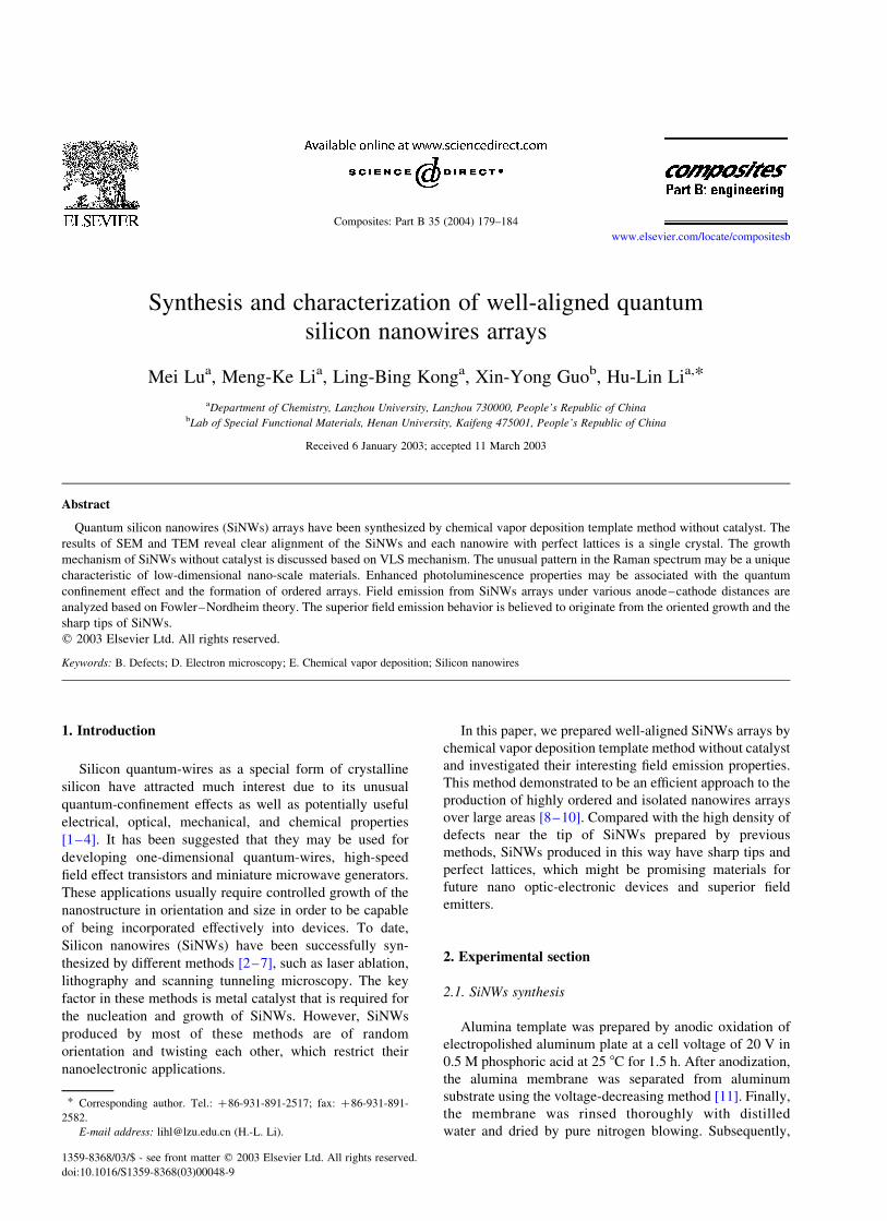
Fig. 1(a) and (b) shows the low magnification cross-
section and the high magnification surface SEM images of
the SiNWs arrays by dissolving alumina, respectively. It is
found that the nanowires were very straight and in a good
alignment. A sharp tip was also found at the end of each
nanowire, which will be beneficial to a field emitter. In the
mean time, there is a silicon surface film at the bottom of the
SiNWs, which is always obtained in other nanomaterials
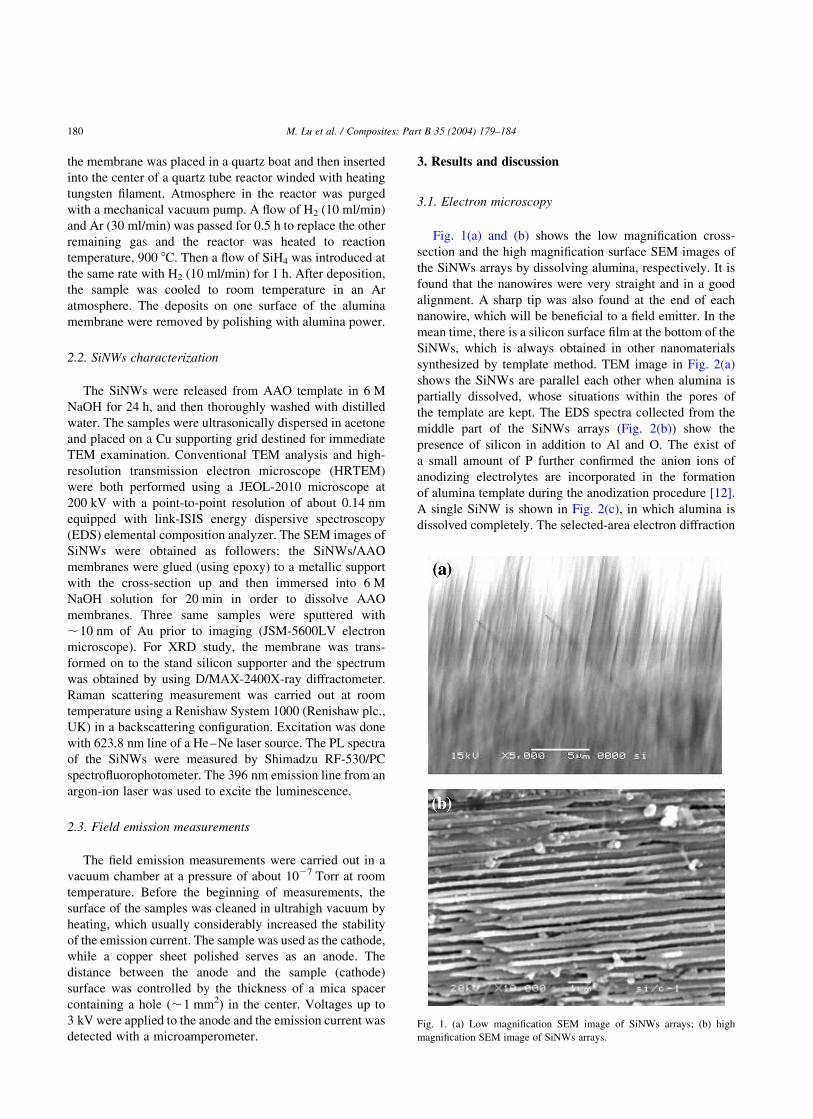
synthesized by template method. TEM image in Fig. 2(a)
shows the SiNWs are parallel each other when alumina is
partially dissolved, whose situations within the pores of
the template are kept. The EDS spectra collected from the
middle part of the SiNWs arrays (Fig. 2(b)) show the
presence of silicon in addition to Al and O. The exist of
a small amount of P further confirmed the anion ions of
anodizing electrolytes are incorporated in the formation
of alumina template during the anodization procedure [12].
A single SiNW is shown in Fig. 2(c), in which alumina is
dissolved completely. The selected-area electron diffraction
Fig. 1. (a) Low magnification SEM image of SiNWs arrays; (b) high
magnification SEM image of SiNWs arrays.
M. Lu et al. / Composites: Part B 35 (2004) 179–184180
(SAED) pattern taken from this SiNW is shown in Fig. 2(d).
It can be seen that the diffraction spots are organized in an
almost precise hexagon or parallelogram, indicating that the
diamond lattice structure of bulk Si is also preserved in the
SiNWs. According to the geometry analyses of electron
diffraction, the cubic indices of the diffraction spots are
demarcated. To confirm the results, other SiNWs were
selected to perform the SAED experiments and the same
results were obtained. Therefore, it can be concluded that
each single SiNW is a single crystal.
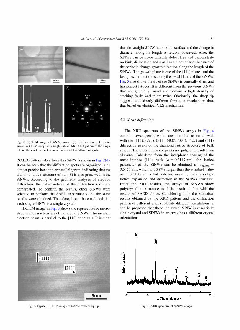
HRTEM image in Fig. 3 shows the representative micro-
structural characteristics of individual SiNWs. The incident
electron beam is parallel to the [110] zone axis. It is clear
that the straight SiNW has smooth surface and the change in
diameter along its length is seldom observed. Also, the
SiNWs can be made virtually defect free and demonstrate
no kink, dislocation and small angle boundaries because of
the periodic change growth direction along the length of the
SiNWs. The growth plane is one of the (111) planes and the
fast growth direction is along the [2211] axis of the SiNWs.
Fig. 3 also shows the tip of the SiNWs is generally sharp and
has perfect lattices. It is different from the previous SiNWs
that are generally round and contain a high density of
stacking faults and micro-twins. Obviously, the sharp tip
suggests a distinctly different formation mechanism than
that based on classical VLS mechanism.
3.2. X-ray diffraction
The XRD spectrum of the SiNWs arrays in Fig. 4
contains seven peaks, which are identified to match well
with the (111), (220), (311), (400), (331), (422) and (511)
diffraction peaks of the diamond lattice structure of bulk
silicon. The other unmarked peaks are judged to result from
alumina. Calculated from the interplanar spacing of the
most intense (111) peak (d ¼ 0:3147 nm), the lattice
parameter of the SiNWs can be obtained as aSiNWs ¼
0:5451 nm; which is 0.387% larger than the standard value
aSi ¼ 0:5430 nm for bulk silicon, revealing there is a slight
lattice expansion and distortion in the SiNWs structure.
From the XRD results, the arrays of SiNWs show
polycrystalline structure as if the result conflict with the
results of SAED above. Considering it is the statistical
results obtained by the XRD pattern and the diffraction
pattern of different grains indicate different orientations, it
can be proposed that these individual SiNW is essentially
single crystal and SiNWs in an array has a different crystal
orientation.
Fig. 2. (a) TEM image of SiNWs arrays; (b) EDS spectrum of SiNWs
arrays; (c) TEM image of a single SiNW; (d) SAED pattern of the single
SiNW, the inset data is the cubic indices of the diffractive spots.
Fig. 3. Typical HRTEM image of SiNWs with sharp tip. Fig. 4. XRD spectrum of SiNWs arrays.
M. Lu et al. / Composites: Part B 35 (2004) 179–184 181
3.3. Possible mechanism
It is clear that the conventional VLS mechanism [13,14]
could not explain the growth of SiNWs, because catalyst is
no longer required in the deposition. We consider it is
probably because there are a large of Lewis acid nature of
surface sites in amorphous and transition alumina and these
sites have the intrinsic catalytic activity of transition
alumina in front of the decomposition of SiH4 [15]. It
should be concluded that the internal pore surface within
alumina has a catalytic behavior in addition to its template
effect. Moreover, there are high density of dangling bonds at
the surface of atomic Si, which leads to the bonding with
each other between atomic Si and a continuous diffusion
into the pores of alumina. On the other hand, the carrier gas
Ar will collide with the pore surface and the atomic Si has
absorbed and exchanged energy and momentum with the
atom, causing overcooling at the surface. Because the
precipitation, nucleation and growth of SiNWs always
occurred at the area near the cold fringer, such an
overcooling is important for providing temperature gradient
used as an external driving force for nanowire growth.
Although, it hasn’t been made clear the reason for the
formation of sharp tip on the SiNWs, we believe further
work in the future should be done to interpret this
phenomenon.
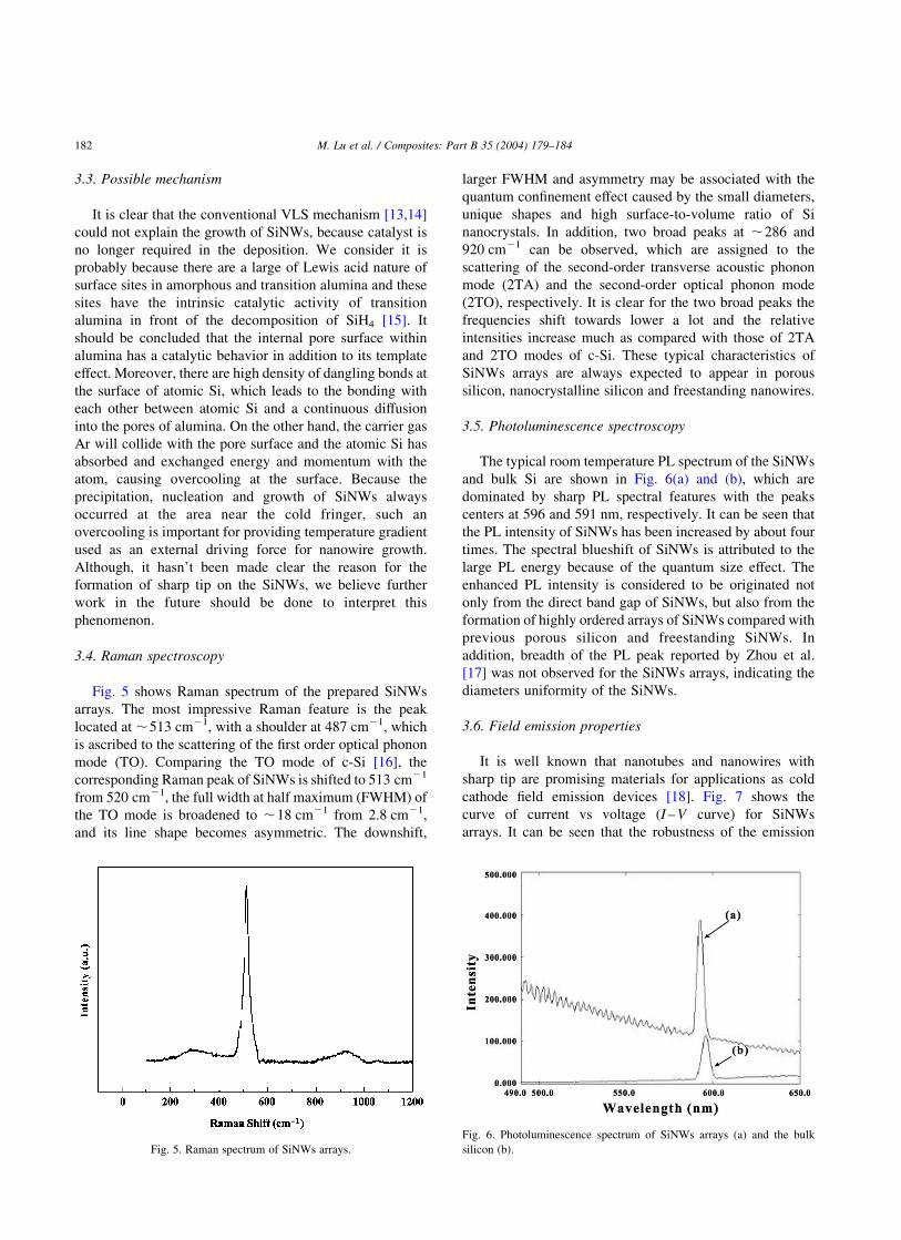
3.4. Raman spectroscopy
Fig. 5 shows Raman spectrum of the prepared SiNWs
arrays. The most impressive Raman feature is the peak
located at ,513 cm21, with a shoulder at 487 cm21, which
is ascribed to the scattering of the first order optical phonon
mode (TO). Comparing the TO mode of c-Si [16], the
corresponding Raman peak of SiNWs is shifted to 513 cm21
from 520 cm21, the full width at half maximum (FWHM) of
the TO mode is broadened to ,18 cm21 from 2.8 cm21,
and its line shape becomes asymmetric. The downshift,
larger FWHM and asymmetry may be associated with the
quantum confinement effect caused by the small diameters,
unique shapes and high surface-to-volume ratio of Si
nanocrystals. In addition, two broad peaks at ,286 and
920 cm21 can be observed, which are assigned to the
scattering of the second-order transverse acoustic phonon
mode (2TA) and the second-order optical phonon mode
(2TO), respectively. It is clear for the two broad peaks the
frequencies shift towards lower a lot and the relative
intensities increase much as compared with those of 2TA
and 2TO modes of c-Si. These typical characteristics of
SiNWs arrays are always expected to appear in porous
silicon, nanocrystalline silicon and freestanding nanowires.
3.5. Photoluminescence spectroscopy
The typical room temperature PL spectrum of the SiNWs
and bulk Si are shown in Fig. 6(a) and (b), which are
dominated by sharp PL spectral features with the peaks
centers at 596 and 591 nm, respectively. It can be seen that
the PL intensity of SiNWs has been increased by about four
times. The spectral blueshift of SiNWs is attributed to the
large PL energy because of the quantum size effect. The
enhanced PL intensity is considered to be originated not
only from the direct band gap of SiNWs, but also from the
formation of highly ordered arrays of SiNWs compared with
previous porous silicon and freestanding SiNWs. In
addition, breadth of the PL peak reported by Zhou et al.
[17] was not observed for the SiNWs arrays, indicating the
diameters uniformity of the SiNWs.
3.6. Field emission properties
It is well known that nanotubes and nanowires with
sharp tip are promising materials for applications as cold
cathode field emission devices [18]. Fig. 7 shows the
curve of current vs voltage (I –V curve) for SiNWs
arrays. It can be seen that the robustness of the emission
Fig. 5. Raman spectrum of SiNWs arrays.
Fig. 6. Photoluminescence spectrum of SiNWs arrays (a) and the bulk
silicon (b).
M. Lu et al. / Composites: Part B 35 (2004) 179–184182
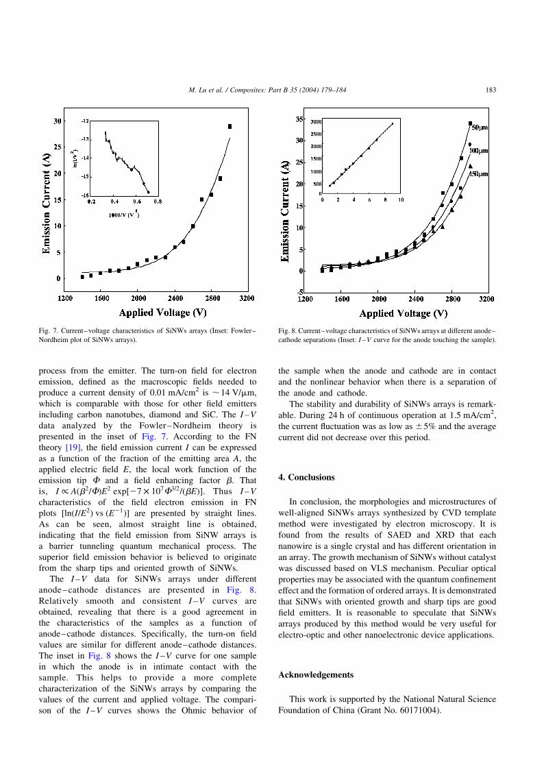
process from the emitter. The turn-on field for electron
emission, defined as the macroscopic fields needed to
produce a current density of 0.01 mA/cm2 is ,14 V/mm,
which is comparable with those for other field emitters
including carbon nanotubes, diamond and SiC. The I –V
data analyzed by the Fowler–Nordheim theory is
presented in the inset of Fig. 7. According to the FN
theory [19], the field emission current I can be expressed
as a function of the fraction of the emitting area A; the
applied electric field E; the local work function of the
emission tip F and a field enhancing factor b: That
is, I / Aðb2=FÞE2 exp½27 £ 107F3=2=ðbEÞ�: Thus I –V
characteristics of the field electron emission in FN
plots ½lnðI=E2Þ vs ðE21Þ� are presented by straight lines.
As can be seen, almost straight line is obtained,
indicating that the field emission from SiNW arrays is
a barrier tunneling quantum mechanical process. The
superior field emission behavior is believed to originate
from the sharp tips and oriented growth of SiNWs.
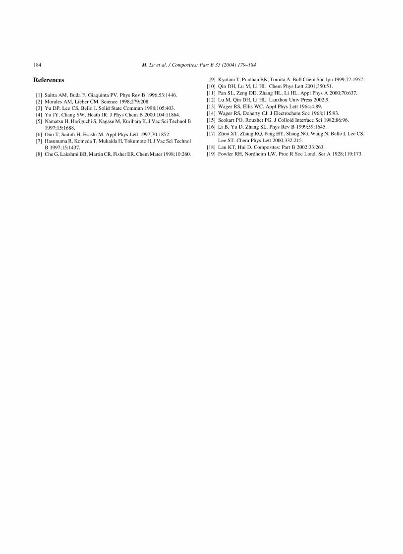
The I –V data for SiNWs arrays under different
anode– cathode distances are presented in Fig. 8.
Relatively smooth and consistent I –V curves are
obtained, revealing that there is a good agreement in
the characteristics of the samples as a function of
anode–cathode distances. Specifically, the turn-on field
values are similar for different anode–cathode distances.
The inset in Fig. 8 shows the I –V curve for one sample
in which the anode is in intimate contact with the
sample. This helps to provide a more complete
characterization of the SiNWs arrays by comparing the
values of the current and applied voltage. The compari-
son of the I –V curves shows the Ohmic behavior of
the sample when the anode and cathode are in contact
and the nonlinear behavior when there is a separation of
the anode and cathode.
The stability and durability of SiNWs arrays is remark-
able. During 24 h of continuous operation at 1.5 mA/cm2,
the current fluctuation was as low as ^5% and the average
current did not decrease over this period.
4. Conclusions
In conclusion, the morphologies and microstructures of
well-aligned SiNWs arrays synthesized by CVD template
method were investigated by electron microscopy. It is
found from the results of SAED and XRD that each
nanowire is a single crystal and has different orientation in
an array. The growth mechanism of SiNWs without catalyst
was discussed based on VLS mechanism. Peculiar optical
properties may be associated with the quantum confinement
effect and the formation of ordered arrays. It is demonstrated
that SiNWs with oriented growth and sharp tips are good
field emitters. It is reasonable to speculate that SiNWs
arrays produced by this method would be very useful for
electro-optic and other nanoelectronic device applications.
Acknowledgements
This work is supported by the National Natural Science
Foundation of China (Grant No. 60171004).
Fig. 7. Current–voltage characteristics of SiNWs arrays (Inset: Fowler–
Nordheim plot of SiNWs arrays).
Fig. 8. Current–voltage characteristics of SiNWs arrays at different anode–
cathode separations (Inset: I –V curve for the anode touching the sample).
M. Lu et al. / Composites: Part B 35 (2004) 179–184 183
References
[1] Saitta AM, Buda F, Giaquinta PV. Phys Rev B 1996;53:1446.
[2] Morales AM, Lieber CM. Science 1998;279:208.
[3] Yu DP, Lee CS, Bello I. Solid State Commun 1998;105:403.
[4] Yu JY, Chang SW, Heath JR. J Phys Chem B 2000;104:11864.
[5] Namatsu H, Horiguchi S, Nagase M, Kurihara K. J Vac Sci Technol B
1997;15:1688.
[6] Ono T, Saitoh H, Esashi M. Appl Phys Lett 1997;70:1852.
[7] Hasunuma R, Komeda T, Mukaida H, Tokumoto H. J Vac Sci Technol
B 1997;15:1437.
[8] Che G, Lakshmi BB, Martin CR, Fisher ER. Chem Mater 1998;10:260.
[9] Kyotani T, Pradhan BK, Tomita A. Bull Chem Soc Jpn 1999;72:1957.
[10] Qin DH, Lu M, Li HL. Chem Phys Lett 2001;350:51.
[11] Pan SL, Zeng DD, Zhang HL, Li HL. Appl Phys A 2000;70:637.
[12] Lu M, Qin DH, Li HL. Lanzhou Univ Press 2002;9.
[13] Wager RS, Ellis WC. Appl Phys Lett 1964;4:89.
[14] Wager RS, Doherty CJ. J Electrochem Soc 1968;115:93.
[15] Scokart PO, Rouxhet PG. J Colloid Interface Sci 1982;86:96.
[16] Li B, Yu D, Zhang SL. Phys Rev B 1999;59:1645.
[17] Zhou XT, Zhang RQ, Peng HY, Shang NG, Wang N, Bello I, Lee CS,
Lee ST. Chem Phys Lett 2000;332:215.
[18] Lau KT, Hui D. Composites: Part B 2002;33:263.
[19] Fowler RH, Nordheim LW. Proc R Soc Lond, Ser A 1928;119:173.
M. Lu et al. / Composites: Part B 35 (2004) 179–184184