Embed Size (px)
Citation preview
Synthesis and Characterization of ZnO/Graphene Nanostructures for Electronics and Photocatalysis
Linköping Studies in Science and TechnologyDissertations No. 2130
Ebrahim Chalangar
Ebrahim Chalangar Synthesis and Characterization of ZnO/Graphene Nanostructures for Electronics and Photocatalysis 2021
FACULTY OF SCIENCE AND ENGINEERING
Linköping Studies in Science and Technology, Dissertation No. 2130Department of Science and Technology, 2021
Linköping UniversitySE-581 83 Linköping, Sweden
www.liu.se

Linköping Studies in Science and Technology Dissertations No. 2130
Synthesis and Characterization of ZnO/Graphene Nanostructures for
Electronics and Photocatalysis
Ebrahim Chalangar
Department of Science and Technology Division of Physics, Electronics and Mathematics
Linköping University, Sweden Norrköping 2021

Cover image:
The cover image shows a cross-sectional SEM image of ZnO nanorods on a CL-
patterned rGO/ZnO:Al seed layer on a Si substrate. The different layers are ar-
tificially colored for a better perspective.
© Ebrahim Chalangar, 2021 (unless otherwise stated)
This work is licensed under the Creative Commons Attribution-
NonCommercial 4.0 International License. To view a copy of this
license, visit http://creativecommons.org/licenses/by-nc/4.0/.
Printed in Sweden by LiU-Tryck, 2021
ISSN: 0345-7524 ISBN: 978-91-7929-682-7

کس نیست که این گوهر تحقیق بسفت ده بیرون ز نهفت این بحر وجود آم
زآن روی که هست، کس نمی داند گفت سودا گفتند هر کس سخنی از سر
The universe has emerged from hidden depths
How? that’s a pearl of wisdom no one has pierced
Everyone has conjectured idly,
But none can describe what it really is
Omar Khayyam – 1131 CE

v
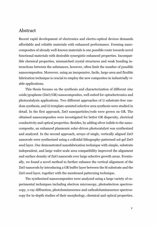
Abstract
Recent rapid development of electronics and electro-optical devices demands
affordable and reliable materials with enhanced performance. Forming nano-
composites of already well-known materials is one possible route towards novel
functional materials with desirable synergistic enhanced properties. Incompat-
ible chemical properties, mismatched crystal structures and weak bonding in-
teractions between the substances, however, often limit the number of possible
nanocomposites. Moreover, using an inexpensive, facile, large-area and flexible
fabrication technique is crucial to employ the new composites in industrially vi-
able applications.
This thesis focuses on the synthesis and characterization of different zinc
oxide/graphene (ZnO/GR) nanocomposites, well suited for optoelectronics and
photocatalysis applications. Two different approaches of i) substrate-free ran-
dom synthesis, and ii) template-assisted selective area synthesis were studied in
detail. In the first approach, ZnO nanoparticles/rods were grown on GR. The
obtained nanocomposites were investigated for better GR dispersity, electrical
conductivity and optical properties. Besides, by adding silver iodide to the nano-
composite, an enhanced plasmonic solar-driven photocatalyst was synthesized
and analyzed. In the second approach, arrays of single, vertically aligned ZnO
nanorods were synthesized using a colloidal lithography-patterned sol-gel ZnO
seed layer. Our demonstrated nanofabrication technique with simple, substrate
independent, and large wafer-scale area compatibility improved the alignment
and surface density of ZnO nanorods over large selective growth areas. Eventu-
ally, we found a novel method to further enhance the vertical alignment of the
ZnO nanorods by introducing a GR buffer layer between the Si substrate and the
ZnO seed layer, together with the mentioned patterning technique.
The synthesized nanocomposites were analyzed using a large variety of ex-
perimental techniques including electron microscopy, photoelectron spectros-
copy, x-ray diffraction, photoluminescence and cathodoluminescence spectros-
copy for in-depth studies of their morphology, chemical and optical properties.

vi
Our findings show that the designed ZnO/GR nanocomposites with vertically
aligned ZnO nanorods of high crystalline quality, synthesized with the devel-
oped low-cost nanofabrication technique, can lead to novel devices offering
higher performance at a significantly lower fabrication cost.
Keywords: zinc oxide, graphene, nanostructure, nanocomposite, conju-
gated electronics, photocatalysis, nanofabrication, colloidal lithography, chem-
ical bath deposition, sol-gel
vii
Populärvetenskaplig sammanfattning
I dag introduceras ny teknik i våra liv i en allt snabbare takt. Nya elektroniska
produkter förväntas underlätta vår vardag genom att göra saker snabbare, mer
exakt, säkrare och billigare. Utvecklingen av nya inbäddade teknologier som In-
ternet-of-things (IoT), 5G-kommunikation, artificiell intelligens och maskinin-
lärning vilar tungt på utvecklingen av ny hårdvara, som i sin tur förutsätter till-
gång till nya avancerade material med förbättrade elektroniska egenskaper och
ett konkurrensmässigt pris.
Att utveckla nya funktionella material med önskvärda egenskaper är en
komplicerad process som involverar olika grenar inom naturvetenskapen, in-
klusive fysik, kemi och materialvetenskap. Att koppla samman etablerad halv-
ledarindustri med nanoteknik är ett utmärkt exempel på detta partnerskap mel-
lan olika vetenskapsområden för bättre materialinnovation. I denna process
skapas ofta nya funktionella material med önskvärda förbättrade egenskaper ge-
nom att integrera konventionella halvledarmaterial med varandra på nya inno-
vativa sätt. Även om detta kan tyckas enkelt i teorin, begränsas utvecklingen i
praktiken ofta av utmaningar som till exempel oförenliga kemiska egenskaper,
olika kristallstrukturer eller inkompatibla elektriska bindningar mellan ämnena
antalet möjliga kombinationer. Dessutom är det viktigt att utveckla nya enkla,
billiga och flexibla tillverkningsmetoder för storskalig produktion av dessa nya
kompositmaterial.
Den här avhandlingen fokuserar på utveckling av nya funktionella nano-
kompositer, bestående av halvledarmaterialet zinkoxid (ZnO) och det två-di-
mensionella materialet grafen, för tillämpningar inom optoelektronik och foto-
katalys. Zinkoxid kan odlas som tunna nålliknande strukturer som kallas nanos-
tavar med en billig lösningsbaserad teknik. Tack vare sina utmärkta elektriska
och optiska egenskaper har ZnO använts flitigt i många applikationer som till
exempel lysdioder, elektrokemiska sensorer och gassensorer. Grafen har ut-
märkt sig som ett fantastiskt material med helt unika elektriska, optiska och me-
kaniska egenskaper som väsentligt förbättrar den optoelektroniska och fotoka-
talytiska effektiviteten hos ZnO/grafen nanokompositer.

viii
Jag har i mitt arbete studerat elektrisk ledningsförmåga, optiska egen-
skaper och fotokatalyseffektivitet hos våra designade ZnO/grafen nanokompo-
siter under simulerad solstrålning. Dessutom har jag odlat vertikalt ordnade
ZnO nanostavar i små nanohål på mönstrade substrat belagda med ett tunt lager
av antingen ZnO, eller med ett sandwichlager bestående av ZnO och grafen med
hjälp av en ny billig metod som kallas kolloidal litografi. Denna tillverkningsme-
tod erbjuder enkel odling av högkvalitativa (kristallina) ZnO nanostavar med
god kontroll över ytdensiteten på stora godtyckliga materialytor. Våra resultat
visar att dessa nya högkvalitativa ZnO/grafen nanokompositer potentiellt erbju-
der en ny materialplattform för tillverkning av exempelvis billig högpresterande
optoelektronik.
ix
Acknowledgment
The past five years were the most challenging but exciting part of my life. Many
people helped me during this journey, although only one name appears on the
cover of this thesis. I would like to express my sincere gratitude to all of you.
My main supervisor Håkan Pettersson for giving me the opportunity and
freedom to work on this project. Not only did I learn scientific matters from you,
but also your precision, tolerance and respectful behavior will be my intentions.
I always felt comfortable working with you during these years, oh wait…! maybe
I should exclude the deadline times.
My co-supervisors, Magnus Willander and Omer Nour, for all your
supports, encouragement, fruitful discussions, and always accessible communi-
cation. Also, thanks go to the lab crew, Lars Gustavsson, Thomas Karlsson
and Meysam Karami, for keeping the lab running.
I also would like to thank my colleagues at Halmstad University. Emil
Nilsson, who taught me the very basics of RF components and measurements,
and also for assisting me on the first days after I arrived in Sweden. Pererik
Andreasson for all his support and always pleasant discussions. Jessika Ros-
enberg and Stefan Gunnarsson for all their help with administrative issues.
I especially thank Struan Gray for revising this thesis.
Also, I appreciate all my former and current friends at Halmstad University
and Linköping University.
Being a PhD student not only shaped my life but also affected my beloveds’
lives. With my deepest gratitude, I wish the best for my mother and my father,
who endured the distance to us and their grandchildren during these years, and
for my wife for her endless love and kind support.
Ebrahim Chalangar,
Linköping, March 2021
x
List of publications
Papers included in this thesis:
Paper I.
Influence of Morphology on Electrical and Optical Properties of Gra-phene/Al-Doped ZnO-Nanorod Composites Ebrahim Chalangar, Houssaine Machhadani, Seung-Hyuk Lim, K. Fredrik Karlsson, Omer Nur, Magnus Willander, and Håkan Pettersson. Nanotechnology, 2018. https://doi.org/10.1088/1361-6528/aad3ec.
Contribution: I prepared and characterized the samples and wrote the first draft. I was actively involved in conceiving the research idea and analyzing the results.
Paper II.
Graphene-Based Plasmonic Nanocomposites for Highly Enhanced Solar-Driven Photocatalytic Activities Rania E. Adam‡, Ebrahim Chalangar‡, Mahsa Pirhashemi, Galia Pozina, Xianjie Liu, Justinas Palisaitis, Håkan Pettersson, Magnus Willander, and Omer Nur. RSC Advances, 2019. https://doi.org/10.1039/C9RA06273D. (‡ Both co-first author)
Contribution: I took part in material synthesizing and performed the electron microscopy analysis. I contributed to analyzing the data, writing the first draft and revising the final manuscript.
Paper III.
Synthesis of Vertically Aligned ZnO Nanorods Using Sol-Gel Seeding and Colloidal Lithography Patterning Ebrahim Chalangar, Omer Nur, Magnus Willander, Anders Gustafsson, and Håkan Pettersson. Nanoscale Research Letters, 2021. https://doi.org/10.1186/s11671-021-03500-7.
Contribution: I prepared and characterized the samples and wrote the first draft. I was actively involved in conceiving the research idea, analyzing the results, and revising the final manuscript.
xi
Paper IV.
Nanopatterned reduced graphene oxide/Al-doped ZnO seed layer for vertical growth of single ZnO nanorods on various substrates Ebrahim Chalangar, Elfatih Mustafa, Omer Nur, Magnus Willander, Anders Gustafsson and Håkan Pettersson. In manuscript
Contribution: I prepared and characterized the samples and wrote the first draft. I was actively involved in conceiving the research idea, analyzing the results, and revising the final manuscript.
Papers not included in this thesis:
Efficient Photo Catalysts Based on Silver Doped ZnO Nanorods for the Photo Degradation of Methyl Orange Muhammad Ali Bhatti, Aqeel Ahmed Shah, Khalida Faryal Almani, Aneela Ta-hira, Seyed Ebrahim Chalangar, Ali dad Chandio, Omer Nur, Magnus Willander, and Zafar Hussain Ibupoto. Ceramics International, 2019. https://doi.org/10.1016/j.cera-mint.2019.08.027.
Contribution: I was involved in sample preparation for electron microscopy, performed the SEM and EDS measurements and read the final manuscript.
Facile Synthesis of Copper Doped ZnO Nanorods for the Efficient Photo Degradation of Methylene Blue and Methyl Orange
Aqeel Ahmed Shah, Muhammad Ali Bhatti, Aneela Tahira, Ali Dad Chandio, Iftikhar A. Channa, Ali Ghulam Sahito, Ebrahim Chalangar, Magnus Willander, Omer Nur, and Zafar Hussain Ibupoto. Ceramics International, 2020. https://doi.org/10.1016/j.cera-mint.2019.12.024.
Contribution: I was involved in sample preparation for electron microscopy, performed the SEM and EDS measurements and read the final manuscript.


xiii
Table of Contents
Abstract ................................................................................................................. v Populärvetenskaplig sammanfattning .............................................................. vii Acknowledgment .................................................................................................ix List of publications ............................................................................................... x Table of Contents .............................................................................................. xiii 1 Introduction ............................................................................................... 17
1.1 Zinc oxide/graphene nanocomposites ............................................ 18 1.2 Zinc oxide/graphene heterostructures ............................................ 20 1.3 Thesis Aim and Outline ................................................................... 21
2 Materials background ................................................................................ 23 2.1 Semiconductors and electronic band structure .............................. 23 2.2 Zinc oxide ......................................................................................... 24
2.2.1 Defect levels in ZnO ................................................................ 25 2.2.2 Doping of ZnO ......................................................................... 26 2.2.3 Polarity in ZnO nanorods ....................................................... 27 2.2.4 Surface defects and band bending in ZnO nanorods ............. 28
2.3 Graphene and graphene oxide ......................................................... 29 2.4 ZnO-graphene heterojunctions ....................................................... 31
3 Zinc oxide-graphene nanocomposites ...................................................... 33 3.1 Synthesis method ............................................................................. 33
3.1.1 Chemical bath deposition of ZnO nanorods ........................... 34 3.1.2 ZnO nanoparticles growth on GR nanoplates ........................ 36 3.1.3 Aluminum doping in ZnO ....................................................... 37 3.1.4 Adding silver iodide into ZnO/GR nanocomposites .............. 38
3.2 Characterization methods ............................................................... 39
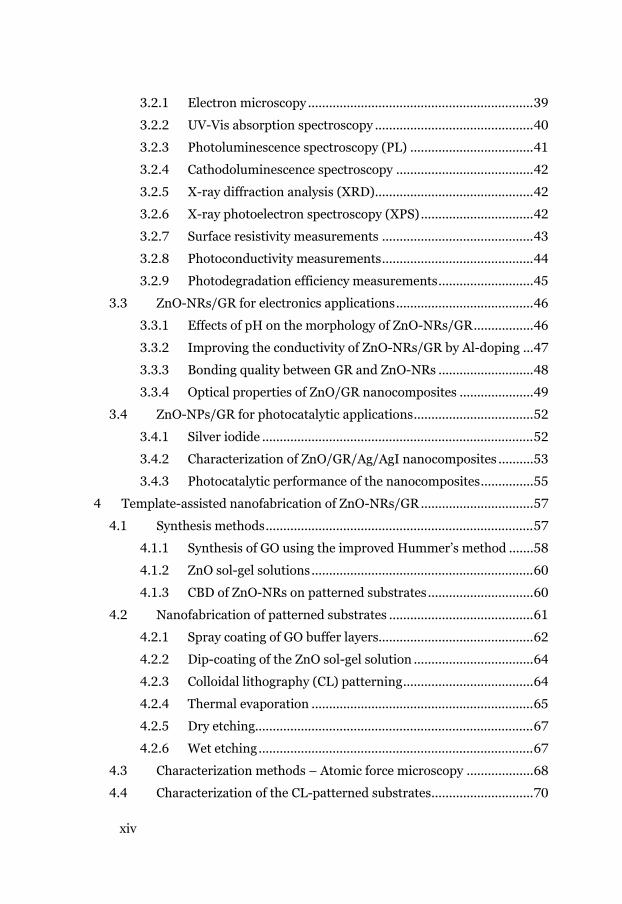
xiv
3.2.1 Electron microscopy ................................................................ 39 3.2.2 UV-Vis absorption spectroscopy ............................................. 40 3.2.3 Photoluminescence spectroscopy (PL) ................................... 41 3.2.4 Cathodoluminescence spectroscopy ....................................... 42 3.2.5 X-ray diffraction analysis (XRD) ............................................. 42 3.2.6 X-ray photoelectron spectroscopy (XPS) ................................ 42 3.2.7 Surface resistivity measurements ........................................... 43 3.2.8 Photoconductivity measurements ........................................... 44 3.2.9 Photodegradation efficiency measurements ........................... 45
3.3 ZnO-NRs/GR for electronics applications ....................................... 46 3.3.1 Effects of pH on the morphology of ZnO-NRs/GR ................. 46 3.3.2 Improving the conductivity of ZnO-NRs/GR by Al-doping ... 47 3.3.3 Bonding quality between GR and ZnO-NRs ........................... 48 3.3.4 Optical properties of ZnO/GR nanocomposites ..................... 49
3.4 ZnO-NPs/GR for photocatalytic applications .................................. 52 3.4.1 Silver iodide ............................................................................. 52 3.4.2 Characterization of ZnO/GR/Ag/AgI nanocomposites .......... 53 3.4.3 Photocatalytic performance of the nanocomposites ............... 55
4 Template-assisted nanofabrication of ZnO-NRs/GR ................................ 57 4.1 Synthesis methods ............................................................................ 57
4.1.1 Synthesis of GO using the improved Hummer’s method ....... 58 4.1.2 ZnO sol-gel solutions ............................................................... 60 4.1.3 CBD of ZnO-NRs on patterned substrates .............................. 60
4.2 Nanofabrication of patterned substrates ......................................... 61 4.2.1 Spray coating of GO buffer layers............................................ 62 4.2.2 Dip-coating of the ZnO sol-gel solution .................................. 64 4.2.3 Colloidal lithography (CL) patterning ..................................... 64 4.2.4 Thermal evaporation ............................................................... 65 4.2.5 Dry etching............................................................................... 67 4.2.6 Wet etching .............................................................................. 67
4.3 Characterization methods – Atomic force microscopy ................... 68 4.4 Characterization of the CL-patterned substrates ............................. 70

xv
4.4.1 Why using Si/GO substrates? ................................................. 70 4.4.2 Improved ZnO seed layers by dip-coating .............................. 71 4.4.3 Reduced GO/Al-doped ZnO seed layers ................................. 73 4.4.4 Distribution of polystyrene nanobeads on surfaces ............... 73
5 Conclusions and Outlook ........................................................................... 77 References .......................................................................................................... 79 Part II: Papers .................................................................................................... 89

17
1 Introduction
Today, electronic devices are evolving very rapidly, with greater functionality
and faster and more reliable operations. This progress has affected our daily
lives and led to further integration of the latest technologies into various aspects
of our lives. The Internet-of-things (IoT), comprised of novel embedded systems
with a massive number of collective sensors, is now being marketed to assist
with health, education, transportation, and many more. 5G-communication,
with its remarkable predicted advantages, provides the faster, ultra-reliable, and
massive wireless connection between devices that is demanded by other appli-
cations. In step with the expansion of these technologies, the need for more en-
ergy, and the consequent increase in environmental pollution, become more
pronounced. So, the future of sustainable growth relies on developing more ef-
ficient hardware to balance requirements with resources. To improve devices’
efficiency, additional new functional materials are required. The new devices
should also be affordable and inexpensive to facilitate widespread adoption of
new massively embedded applications.
Despite all efforts, the range of materials with the desired electrical and op-
tical properties is still limited by their functionality or cost. One way to overcome
these challenges is to develop new composites of already existing, well-known
materials with desirable synergistic enhanced properties. In fact, recent ad-
vances in nanotechnology have provided more insights towards a better under-
standing and implementation of novel composite materials in various applica-
tions. This thesis particularly deals with semiconductor materials with nanome-
ter-scale dimensions and their composition with other nano-electronic materi-
als.
Introduction
18
Research into innovative nanocomposite materials and their new applica-
tions has attracted much recent interest and effort. A vast number of metal-sem-
iconductor [1], multiple metal oxides [2], and organic-inorganic [3] nanocom-
posites with improved properties have been generated and used in broad fields
of applications such as energy, hydrogen evolution, the environment, disinfec-
tion and purification. A combination of semiconductors and 2D materials such
as graphene (GR) is another exciting class of composite materials with promis-
ing characteristics for photocatalysis, sensors, energy, and electronic applica-
tions [4]. To date, various such nanocomposites, including group IV (Si), group
II-VI (ZnO, ZnS), group III-V (GaAs, GaN), and metal oxide semiconductors
(TiO2, ITO), have been realized [4].
The research presented in this thesis is mainly focused on the possible com-
posites of zinc oxide (ZnO) and GR, exploring their fundamental properties and
realizing their potential applications in electronics and photocatalysis. The ma-
terials were selected based on their suitable intrinsic optical and electrical prop-
erties for the mentioned applications. Individually, these two well-known mate-
rials have been thoroughly investigated in many previous studies. But the com-
bination of the two has recently gained popularity due to the resulting synergis-
tic enhanced properties, which are not available in each of the single materials.
1.1 Zinc oxide/graphene nanocomposites
Composites of ZnO and GR have been realized in several research reports [5–8]
with strong evidence of a good crystal growth compatibility due to excellent
matching of their crystal lattices [9–11]. Growth of various ZnO structures on a
GR surface in the forms of nanoparticles (0D) and nanorods (1D) can be found
in the literature, prepared by various higher-temperature, vacuum-required, or
solution-based growth techniques. Also, a wide range of applications of these
composite materials in electronics, optoelectronics, photovoltaics, and sensors
have been demonstrated [4]. Despite these efforts, a research gap between the
optimal functionality and the fabrication simplicity of ZnO/GR is still observa-
ble. In other words, in the majority of the reports, production of high-
Zinc oxide/graphene nanocomposites
19
performance ZnO/GR nanostructures usually required sophisticated methods,
leading to more expensive products. Further developments in the nanocompo-
site’s growth procedure with significant control over the final structure are cru-
cially needed to meet the criteria of optimal desired properties and low-cost pro-
duction. This is what motived us to conduct this research work.
This PhD study, therefore, probes ways to fill this gap by combining a sim-
ple growth technique and precisely designing the ZnO/GR structures suited for
electronics or as a photocatalyst. Growth of different morphologies of ZnO on
the GR nanoplates was achieved, and the nanocomposites were investigated for
higher electrical conductivity, optical properties, and enhanced photocatalytic
efficiency. Moreover, we pursued a method to fully control the final structures
of the nanocomposites with respect to their density, alignment, ordering, and
feature size, using colloidal lithography and optimized seed layers.
Our results show successful growth of Al-doped ZnO nanorods (NRs) on GR
nanoplatelets with optimized porosity and electrical conductivity, suitable for
electronic applications in which inexpensive large-volume of conductive mate-
rials are required, e.g., 3D printing. Also, highly efficient solar-driven photocata-
lysts of ZnO, GR and silver iodide (AgI) for removing organic pollutants from
water were achieved and exhibited. Additionally, a novel nanofabrication
method of vertically aligned ZnO nanorods on different substrates, using a com-
bination of colloidal lithography and sol-gel seeded layers, was demonstrated.
Our findings are important for further understanding the basic charge car-
rier transport mechanism in the semiconductor-graphene interfaces, photocar-
rier generation and recombination, and energy defect levels in the ZnO/GR
nanocomposites. The results can be used to tailor the conductivity of future 3D-
printable material with large volumes and inexpensive porous structures. Also,
the solar-driven photocatalysts developed here are beneficial for environmental
purification since they can remove organic pollutants from water using the en-
ergy in sunlight. Moreover, our nanofabrication method offers a simple and in-
expensive solution for controlling the NRs’ growth and enhancing their align-
ment with substrate-independent flexibility. Finally, our work can help to pro-
duce cheaper, porous, conjugated graphene-semiconductor composites to
Introduction
20
fabricate high-performance devices where vertically ordered ZnO-NRs of high
crystalline quality are essential.
1.2 Zinc oxide/graphene heterostructures
Similar to conventional metal-semiconductor junctions, GR-semiconductor
junctions generally show rectifying characteristics [12]. When two materials are
atomically close to each other, a junction is formed at their interface. The type
of junction depends on the similarity of the crystal structure, e.g., bandgap dif-
ference, valence band matching, lattice mismatch, and the type and level of dop-
ing in the two materials. If the materials are the same, a homojunction is formed
at the interface, for example, a p-n junction of a semiconductor with different
donor and acceptor dopants.
A heterojunction forms at the interface of two dissimilar semiconductor
materials, usually by heteroepitaxial growth of fairly lattice-matched semicon-
ductors on top of each other. The crystal lattice mismatch is the limiting param-
eter for the epitaxial growth, inducing atomic displacements (strain) and dislo-
cations at the interface unless the epitaxial layer is extremely thin. As a result of
the difference in bandgap energy and the band alignments at the interface, such
heterojunctions are the building-blocks for many interesting applications, in-
cluding laser diodes, light-emitting diodes (LEDs), resonant tunneling diodes,
photodetectors, and solar cells.
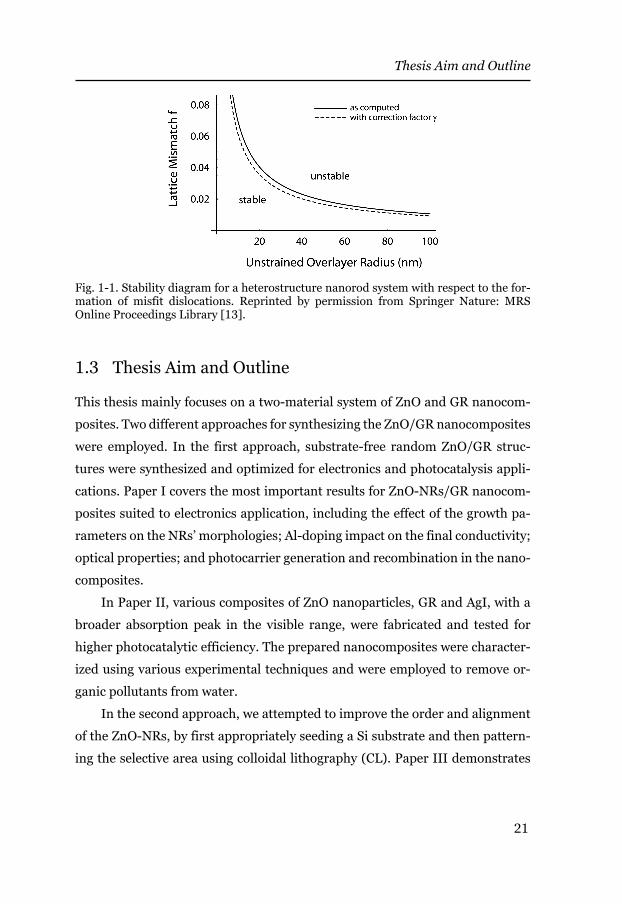
The lattice mismatch between the joint materials can be tolerated if lower-
dimensional materials, e.g., nanoparticles (0D) or nanorods (1D), with a lower
interfacial area, are used. In this case, the strain energy at the heterojunction is
relieved via elastic relaxations, leading to more stable structures [13, 14]. The
stability of the structure depends on the lattice mismatch factor and the size of
the interfacial area, or equivalently, the diameter of the grown particles. Fig. 1-1
shows a typical stability diagram for a heterostructure nanorod system with two
stable and unstable regions, depending on the NRs’ diameter and the lattice mis-
match factor. The nanoparticle and nanorod morphologies of ZnO in our devel-
oped nanocomposites were chosen based on this consideration.
Thesis Aim and Outline
21
Fig. 1-1. Stability diagram for a heterostructure nanorod system with respect to the for-mation of misfit dislocations. Reprinted by permission from Springer Nature: MRS Online Proceedings Library [13].
1.3 Thesis Aim and Outline
This thesis mainly focuses on a two-material system of ZnO and GR nanocom-
posites. Two different approaches for synthesizing the ZnO/GR nanocomposites
were employed. In the first approach, substrate-free random ZnO/GR struc-
tures were synthesized and optimized for electronics and photocatalysis appli-
cations. Paper I covers the most important results for ZnO-NRs/GR nanocom-
posites suited to electronics application, including the effect of the growth pa-
rameters on the NRs’ morphologies; Al-doping impact on the final conductivity;
optical properties; and photocarrier generation and recombination in the nano-
composites.
In Paper II, various composites of ZnO nanoparticles, GR and AgI, with a
broader absorption peak in the visible range, were fabricated and tested for
higher photocatalytic efficiency. The prepared nanocomposites were character-
ized using various experimental techniques and were employed to remove or-
ganic pollutants from water.
In the second approach, we attempted to improve the order and alignment
of the ZnO-NRs, by first appropriately seeding a Si substrate and then pattern-
ing the selective area using colloidal lithography (CL). Paper III demonstrates

Introduction
22
the patterning technique and the seed layer preparation method used later in
Paper IV to fabricate the GR/ZnO-NRs vertically aligned nanostructures.
The thesis places all the experimental achievements in a united context by
providing background information in Chapter 2, along with more details about
the experiments and the analytical techniques employed. Chapter III deals with
Papers I and II, describing the use of ZnO/GR nanocomposites as a conductive,
printable material and a photocatalyst. Chapter IV introduces the CL-patterning
technique and summarizes the work reported in Papers III and IV. Finally, my
PhD research is concluded in Chapter V, followed by a discussion of future chal-
lenges and outlooks.
23
2 Materials background
Before going into our nanocomposite synthesis process in detail, an introduc-
tion to the basic concepts of semiconductors, including heterostructures, energy
levels, defects, and doping, is given here. This chapter aims to familiarize the
reader with the concepts that will be used later, and summarizes what I learned
during my experimental research.
2.1 Semiconductors and electronic band structure
Although conductors conduct electrical currents very well, semiconductors are
the most exciting materials in electronics. The difference between conductors
and semiconductors comes from their atomic structure and the electronic con-
figuration in their crystal lattices. Atoms of an element can form chemical bonds
with each other and arrange themselves in a periodic crystal lattice by reforming
their electron orbitals to a hybrid orbital configuration. The periodic atom posi-
tions introduce a periodic electric potential in the crystal lattice. By applying
Bloch’s theorem and solving Schrödinger’s equation in the tight-binding model,
including spin-orbit coupling, the material’s electronic band structure can be
derived. Detailed equations are to be found in most solid-state textbooks, and
only the most important results are given here.
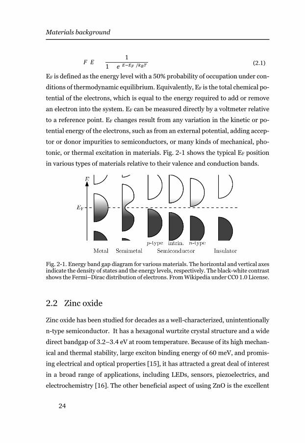
The electronic band structure of a crystalline solid is determined by the den-
sity of states in its different energy levels, including the valence band (Ev), con-
duction band (Ec), and the bandgap (Eg), which has zero density of states. The
electrons fill the available energy levels from lower to higher energies according
to the Pauli principle, which results in the well-known Fermi–Dirac distribution
function (Eq. (2.1)) at a given temperature (T), where kB is the Boltzmann’s con-
stant and EF is the Fermi energy level.
Materials background
24
𝐹𝐹(𝐸𝐸) =1
1 + 𝑒𝑒(𝐸𝐸−𝐸𝐸𝐹𝐹)/𝑘𝑘𝐵𝐵𝑇𝑇 (2.1)
EF is defined as the energy level with a 50% probability of occupation under con-
ditions of thermodynamic equilibrium. Equivalently, EF is the total chemical po-
tential of the electrons, which is equal to the energy required to add or remove
an electron into the system. EF can be measured directly by a voltmeter relative
to a reference point. EF changes result from any variation in the kinetic or po-
tential energy of the electrons, such as from an external potential, adding accep-
tor or donor impurities to semiconductors, or many kinds of mechanical, pho-
tonic, or thermal excitation in materials. Fig. 2-1 shows the typical EF position
in various types of materials relative to their valence and conduction bands.
Fig. 2-1. Energy band gap diagram for various materials. The horizontal and vertical axes indicate the density of states and the energy levels, respectively. The black-white contrast shows the Fermi–Dirac distribution of electrons. From Wikipedia under CC0 1.0 License.
2.2 Zinc oxide
Zinc oxide has been studied for decades as a well-characterized, unintentionally
n-type semiconductor. It has a hexagonal wurtzite crystal structure and a wide
direct bandgap of 3.2–3.4 eV at room temperature. Because of its high mechan-
ical and thermal stability, large exciton binding energy of 60 meV, and promis-
ing electrical and optical properties [15], it has attracted a great deal of interest
in a broad range of applications, including LEDs, sensors, piezoelectrics, and
electrochemistry [16]. The other beneficial aspect of using ZnO is the excellent
Zinc oxide
25
flexibility in growth techniques and the various possible morphologies of nano-
particles (NPs), NRs and thin films. In the following section, the defects and do-
pants in a ZnO crystal, which are the main origin of its electrical and optical
characteristics, are briefly reviewed.
2.2.1 Defect levels in ZnO
During the ZnO growth process, various defects may be introduced in the crystal
lattice, with corresponding defect energy levels in the ZnO band structure. Do-
nor-like defects of oxygen vacancy (VO) and interstitial zinc (Zni), and acceptor-
like defects of zinc vacancy (VZn) and interstitial oxygen (Oi) are the most likely
native point defects in ZnO.
In many publications, the unintentionally n-type conductivity of ZnO has
been attributed to the VO and Zni, but more accurate studies have shown that
these point defects cannot be the cause of the n-type behavior, as neither en-
gaged in the conductivity [17]. The reason is that the donor-like native defects
in ZnO are either deep level donors or have a high formation energy and so a
very low formation probability [17–19]. In general, only the shallow defect lev-
els, close to the band edges, can be thermally ionized at room temperature and
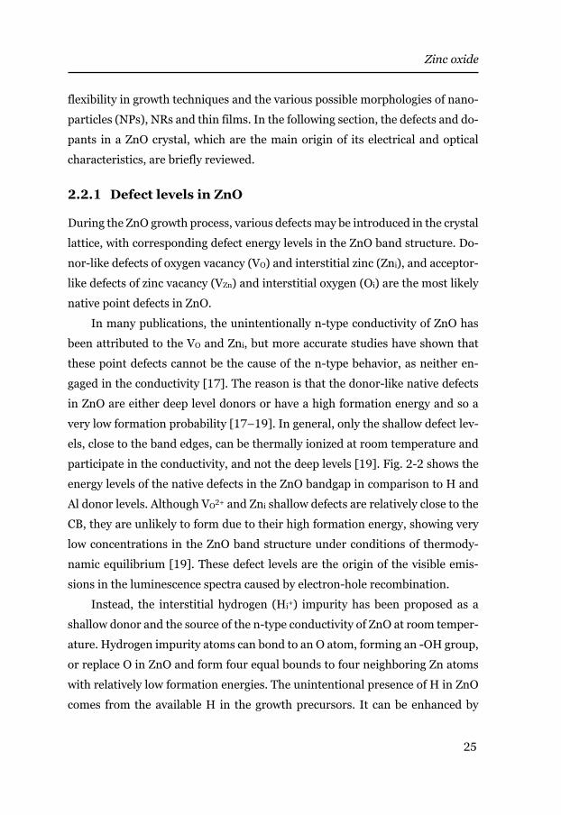
participate in the conductivity, and not the deep levels [19]. Fig. 2-2 shows the
energy levels of the native defects in the ZnO bandgap in comparison to H and
Al donor levels. Although VO2+ and Zni shallow defects are relatively close to the
CB, they are unlikely to form due to their high formation energy, showing very
low concentrations in the ZnO band structure under conditions of thermody-
namic equilibrium [19]. These defect levels are the origin of the visible emis-
sions in the luminescence spectra caused by electron-hole recombination.
Instead, the interstitial hydrogen (Hi+) impurity has been proposed as a
shallow donor and the source of the n-type conductivity of ZnO at room temper-
ature. Hydrogen impurity atoms can bond to an O atom, forming an -OH group,
or replace O in ZnO and form four equal bounds to four neighboring Zn atoms
with relatively low formation energies. The unintentional presence of H in ZnO
comes from the available H in the growth precursors. It can be enhanced by
Materials background
26
annealing the grown ZnO in an H2 atmosphere, resulting in higher electrical
conductivity.
Fig. 2-2. Energy band diagram of native defects and H and Al donor impurities in ZnO. Filled and empty bars represent donor and acceptor levels, respectively. Gathered from Refs. [17–21].
2 . 2 . 2 Doping of ZnO
In addition to the unintentional native defects and H impurity, ZnO can be in-
tentionally doped by group-13 impurities of B, Al, Ga and In, or by F [22].
Among these n-type dopants, Al, with its low formation energy and relatively
low ionization energy of 120 meV (Fig. 2-2), is a promising candidate, particu-
larly in solution-based ZnO growth techniques. High levels of Al-doping, up to
the degenerate level with a carrier concentration of 1020 cm-3, have been
achieved, changing the electrical properties of ZnO from an insulator to a metal.
In contrast to the success achieved with n-type material, p-type doping of ZnO
is notably difficult and still challenging.
As a potential application, Al-doped ZnO (AZO) has been widely studied as
a transparent conductive oxide (TCO) and is presently considered for substitut-
ing conventional TCOs on the market with 85% optical transmittance in the vis-
ible range and electrical resistivity down to 10-3 Ω.cm [23–25]. A comparison of
different TCOs, including AZO, can be found in Ref. [26]. Usually, post-treat-
ments of thermal or UV annealing are required to improve the conductivity of
the final Al-doped ZnO structures.
Zinc oxide
27
The bandgap of ZnO can be changed corresponding to the doping level and
the carrier concentration. The shift of the bandgap is governed by the contribu-
tion of two opposite phenomena, which usually compensate each other: increas-
ing the bandgap proportional to the carrier density (Burstein-Moss effect) and
bandgap narrowing [27].
2.2.3 Polarity in ZnO nanorods
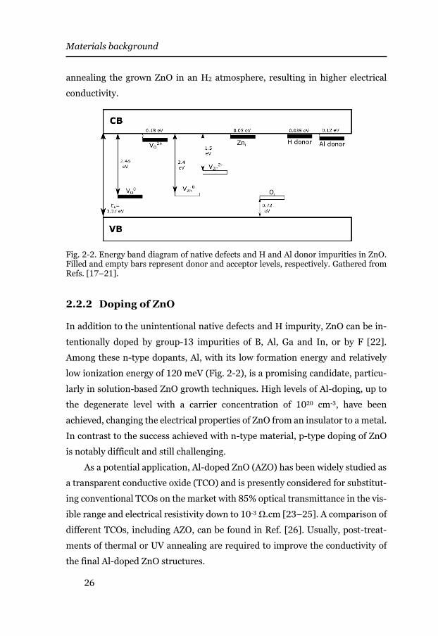
Hexagonal ZnO-NRs exhibit an electric dipolar moment along the c-axis and six
non-polar m-plane sidewalls in [1100] directions with relatively low free surface
energy. The polarity direction is defined as the direction of a vector from the
positively-charged Zn-polar to the negatively-charged O-polar face terminations
at each unit cell (Fig. 2-3). The Zn- and O-polar faces, with various chemical
reactivities, adsorb ambient OH- hydroxyl groups and H+ ions, respectively,
minimizing their free energies and forming a double electrical layer on the sur-
face [28].
Fig. 2-3. O-polar and Zn-polar faces along the c-axis with flipped-over polarities. Re-printed from [29], Copyright 2020 with permission from Elsevier.
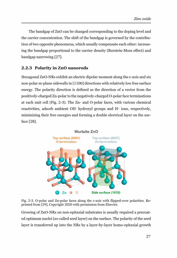
Growing of ZnO-NRs on non-epitaxial substrates is usually required a precoat-
ed optimum nuclei (so-called seed layer) on the surface. The polarity of the seed
layer is transferred up into the NRs by a layer-by-layer homo-epitaxial growth
Materials background
28
of the O- and Zn-polar unit cells on the bottom polar faces. In fact, the polar c-
plane top front is the driving force for the anisotropic one-dimensional growth
of the ZnO-NRs [28]. Thus, any induced surface charge or applied normal-to-
substrate electric field will facilitate the polar alignment and can lead to higher
NRs alignment [30]. Fig. 2-4 shows the polarity transfer from the seed layer into
the grown ZnO nanorods.
The polarity in ZnO-NRs also has a vast influence on the native defects’ spa-
tial distribution within the NRs. It has been shown that the VO defects have a
much smaller formation energy on the non-polar m-plane surfaces, which will
lead to higher VO concentration on the surface of ZnO-NRs [29]. The high sur-
face defect concentration has an important effect on persistent photoconductiv-
ity in ZnO, which is explained below.
Fig. 2-4. Effect of a (a) poorly and a (b) highly polar oriented polycrystalline seed layer on the growth of ZnO-NRs. Reproduced with permission from [31]. © IOP Publishing. All rights reserved.
2.2.4 Surface defects and band bending in ZnO nanorods
Due to the high concentration of VO defects on the ZnO surface, oxygen mole-
cules in the atmosphere are attracted and chemisorbed on the ZnO surface with
a thermal energy barrier of about 0.25 eV [32]. The surface chemisorbed O2 mol-
ecules attract and capture free electrons from the ZnO core. Due to the low con-
centration of free electrons in undoped samples, the electric field inside the sem-
iconductor, induced by the surface chemisorbed ionized O2-, cannot be effec-
tively screened. In this scenario, a built-in electric field is formed near the sur-
face, and the energy bands are bent. Consequently, the area is depleted of free
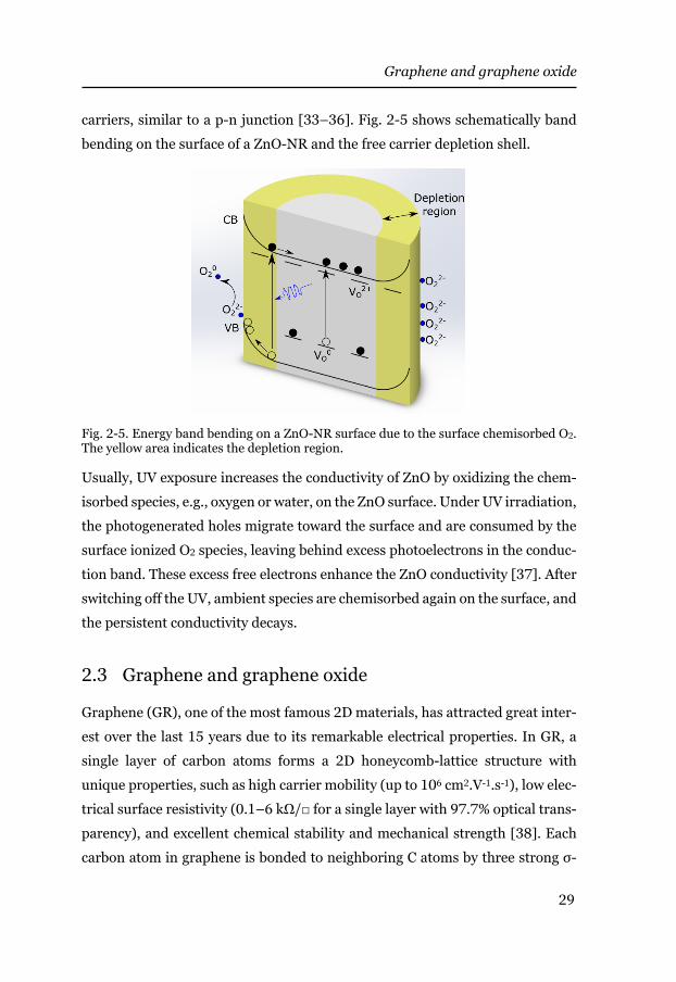
Graphene and graphene oxide
29
carriers, similar to a p-n junction [33–36]. Fig. 2-5 shows schematically band
bending on the surface of a ZnO-NR and the free carrier depletion shell.
Fig. 2-5. Energy band bending on a ZnO-NR surface due to the surface chemisorbed O2. The yellow area indicates the depletion region.
Usually, UV exposure increases the conductivity of ZnO by oxidizing the chem-
isorbed species, e.g., oxygen or water, on the ZnO surface. Under UV irradiation,
the photogenerated holes migrate toward the surface and are consumed by the
surface ionized O2 species, leaving behind excess photoelectrons in the conduc-
tion band. These excess free electrons enhance the ZnO conductivity [37]. After
switching off the UV, ambient species are chemisorbed again on the surface, and
the persistent conductivity decays.
2.3 Graphene and graphene oxide
Graphene (GR), one of the most famous 2D materials, has attracted great inter-
est over the last 15 years due to its remarkable electrical properties. In GR, a
single layer of carbon atoms forms a 2D honeycomb-lattice structure with
unique properties, such as high carrier mobility (up to 106 cm2.V-1.s-1), low elec-
trical surface resistivity (0.1–6 kΩ/□ for a single la er with 9 . optical trans
parency), and excellent chemical stability and mechanical strength [38]. Each
carbon atom in graphene is bonded to neighboring C atoms b three strong -
Materials background
30
bonds formed of hybridized sp2 orbitals, and an out-of-plane conjugated π-
bond, which is responsible for GR’s electrical conductivity.
The attainable characteristics of GR significantly depend on the layers’ sin-
gularity. As the number of graphene layers is increased, its properties change
dramatically into those of graphite. As a standard arbitrary threshold, backed
up by the International Organization for Standards (ISO), more than ten gra-
phene layers are considered graphite instead of graphene [39]. According to this
standard, graphene as a single layer is abbreviated as 1LG, bilayer graphene as
2LG, and few-layered graphene as FLG.
Graphene can be synthesized using the three main techniques of i) CVD
growth on an appropriate substrate, ii) epitaxial growth on SiC surface, and iii)
exfoliation of graphite flakes [38–40]. The bottom-up CVD and epitaxial growth
techniques typically result in high quality and large wafer-scale areas of single
and multiple-layer graphene films, suitable for high-performance carbon-based
electronic applications. Although these methods are effective in terms of quality,
their potential applications are limited by production costs.
In the other, inexpensive approach, a high volume of GR can be produced
using a top-down, low-cost and facile technique based on exfoliation of bulk
graphite into graphene nanoplates (GNPs). In the chemical exfoliation tech-
nique, chemicals are intercalated between the graphite layers, which weakens
the cohesive van der Waals forces, causing graphite expansion and finally exfo-
liation [41, 42]. The final product of the exfoliation technique consists of a dis-
persion of synthesized graphene oxide (GO) flakes in a liquid, with a range of
different thicknesses and lateral sizes that can further be dried in a powder form.
Despite the simplicity and cost-effectiveness of this method, a significant por-
tion of the final flakes have excess layers due to agglomeration between the par-
ticles. In this research, chemically exfoliated GNP has been used to develop the
other nanocomposites.
Despite all the electrical advantages of GR, it also has disadvantageous
characteristics that make it undesirable for direct use in some applications. Gen-
erally, graphene is highly hydrophobic with a strong tendency not to interact
ZnO-graphene heterojunctions
31
with other materials, making it almost non-dispersible in water or any organic
solvent [43]. In addition, the GNPs undesirably agglomerate into large particles
due to their high aspect-ratio and the existence of van der Waals forces between
the flakes.
On the other hand, GO shows completely different characteristics com-
pared to GR. Due to the presence of high-density oxygen functional groups (in
the range of 40-70% oxygenated carbon atoms [44, 45]) on its surface, GO is
highly water dispersible, easy to interact with, and convenient to process. How-
ever, GO is an insulator and should be reduced to GR after the deposition pro-
cess, usually by strong reductant chemicals like hydrazine, thermally [46], or by
UV irradiation [47].
2.4 ZnO-graphene heterojunctions
As explained in the previous chapter, epitaxial heterostructures are formed by
strong covalent bonding between two dissimilar semiconductors, in which lat-
tice matching is a critical parameter. Alternatively, van der Waals forces be-
tween a 2D material and other materials can also form stable heterostructures
with interesting electronic properties. These van der Waals heterojunctions are
formed by weaker van der Waals interactions between a 2D material and any
passivated, dangling-bond-free material, independent of the lattice matching
[48]. It is worth noting that the charge-transfer mechanism at the interface of
these heterojunctions is by tunneling and hopping of electrons since the band
structure is discontinuous at the interface [48].
In addition to van der Waals interactions, it has been shown that ZnO can
also efficiently be grown on the GR surface [5, 8, 9, 49] with a relatively small
lattice mismatch of about 2% [10, 50]. From an electrical point-of-view, this
fairly well-matched interface between ZnO and graphene can lead to a Schottky
or low-ohmic contact, depending on the doping level and heterojunction band
alignment [7].

33
3 Zinc oxide-graphene nanocomposites
The low cost and simplicity of any novel material fabrication process greatly in-
fluence potential applications of the developed materials. Among different fab-
rication techniques, solution-based methods are simple, inexpensive and en-
ergy-efficient, with important practical industrializing capabilities. The main
advantages of these techniques come from the low-temperature and atmos-
pheric pressure growth conditions. This chapter describes how the chemical
bath deposition technique was used to synthesize various substrate-free
ZnO/GR nanocomposites, mainly developed for electronics and photocatalysis
applications. The synthesized nanocomposites, with random grown structures,
have been investigated for improved dispersity, morphology, electrical and op-
tical properties, and photocatalytic efficiency. Papers I and II address the mate-
rial discussed in this chapter.
3.1 Synthesis method
Several synthesis methods of ZnO-NRs have been realized during the last two
decades. Most of these techniques require high temperature or sophisticated
vacuum equipment for NRs growth that causes the final grown structures to
more expensive, usually harder to industrialize, and applicable to limited areas.
Chemical vapor deposition (CVD) is one of the most reported ZnO-NRs growth
techniques that can provide high-quality NRs at a high-temperature range of
500-950 C, but at atmospheric pressure [51, 52]. The high-temperature growth
limits the usage of some potentially interesting substrates, especially flexible
substrates, in such a growth process. Some other techniques, e.g., pulsed laser
deposition (PLD) [53], vapor-liquid-solid (VLS) [52] and sputtering [54], oper-
ating at high vacuum conditions, result in high crystal quality but with a low
Zinc oxide-graphene nanocomposites
34
deposition rate. Generally, using vacuum deposition techniques raises the pro-
duction cost, and it is not favored in industry.
3.1.1 Chemical bath deposition of ZnO nanorods
Among the available growth techniques, solution-based growth methods, with
advantages including simplicity, low-temperature and atmospheric pressure
growth, are promising for synthesizing materials at a lower cost. Chemical bath
deposition (CBD) and hydrothermal growth (HTG) are the two types of solution-
based growth techniques that sometimes are used conversely by mistake. While
CBD refers to the growth process at low temperature and atmospheric pressure,
HTG indicates the process at a higher temperature and higher pressures, using
a metal or Teflon autoclave.
In CBD of ZnO-NRs, a saturated aqueous solution of the precursors is pre-
pared. Then, an appropriately prepared substrate is suspended in the solution,
and the temperature is elevated to a specific range. The CBD process includes
two steps of nucleation and crystal growth. At the early stages, nuclei sites are
formed by making a solid phase of ZnO from the growth solution. Subsequently,
the ZnO crystal continues to grow epitaxially, forming the final crystal structure.
However, a drawback of the CBD technique is that homogenous nucleation takes
place in the bulk solution, causing many undesired grown structures and higher
wastage of chemicals.
Several Zn precursors, including zinc nitrate, zinc acetate1 and zinc chlo-
ride2, have been investigated for CBD of ZnO, with a strong influence on the final
grown morphologies [55–58]. In this thesis, we have always used an optimized
bath solution of equimolar zinc nitrate3 and hexamethylenetetramine4 (HMT)
for the ZnO-NRs growth. The involved chemical reactions can be summarized
as below:
1 Zn(CH3COO)2.2H2O 2 ZnCl2 3 Zn(NO3)2.6H2O 4 C6H12N4
Synthesis method
35
𝑍𝑍𝑍𝑍(𝑁𝑁𝑂𝑂3)2 → 𝑍𝑍𝑍𝑍2+ + 2𝑁𝑁𝑂𝑂3− (3.1)
𝐶𝐶6𝐻𝐻12𝑁𝑁4 + 6𝐻𝐻2𝑂𝑂 → 6𝐶𝐶𝑂𝑂𝐻𝐻2 + 4𝑁𝑁𝐻𝐻3 (3.2)
𝑁𝑁𝐻𝐻3 + 𝐻𝐻2𝑂𝑂 ⇌ 𝑁𝑁𝐻𝐻4+ + 𝑂𝑂𝐻𝐻− (3.3)
𝑍𝑍𝑍𝑍2+ + 2𝑂𝑂𝐻𝐻− → 𝑍𝑍𝑍𝑍(𝑂𝑂𝐻𝐻)2 (3.4)
𝑍𝑍𝑍𝑍(𝑂𝑂𝐻𝐻)2 → 𝑍𝑍𝑍𝑍𝑂𝑂 + 𝐻𝐻2𝑂𝑂 (3.5)
Dissolving of zinc nitrate and HMT provides Zn2+ and OH- ions in the aqueous
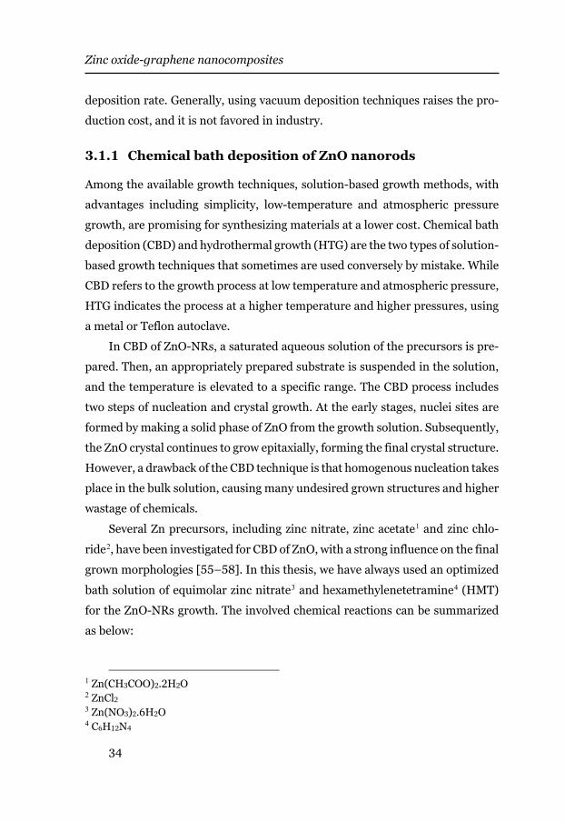
solution (equations (3.1) to (3.3)), respectively. The intermediate species pro-
duced are sensitively dependent on the pH of the solution. Fig. 3-1 shows that
the Zn2+ cations are dominant in the pH range of 6-7, while in a higher pH range
of 10-11, the Zn(II) hydroxide complex ions are more pronounced. During ani-
sotropic c-axis growth of ZnO-NRs, the reactive cations diffuse in the bath solu-
tion and crystallize on the polar c-plane top face of ZnO-NRs.
In our experiment, two different concentrations of 25 mM and 50 mM zinc
nitrate, with the equimolar HMT in DI water, were prepared as the CBD solu-
tion. In addition, the pH of the growth solutions was adjusted to the values of
6.6 and 11 by adding ammonia (NH3). The growth temperature was set to 75 ˚C
and maintained for 2 h. In this approach, the seeded GRs (explained in the next
part) were added to the growth solution under mild stirring.
Fig. 3-1. Ionic species concentrations in different pH values for an aqueous solution of 20 mM of zinc nitrate and HMT at 95 ˚C, Reprinted from [59] under CC BY 4.0 License.
Zinc oxide-graphene nanocomposites
36
3.1.2 ZnO nanoparticles growth on GR nanoplates
The ZnO-NPs were prepared by hydroxylating the Zn2+ in an aqueous solution,
using zinc acetate and KOH. The reaction was performed in the presence of GR,
to grow the NPs directly on the GR surface. First, an ultrasonicated dispersion
of GR in DI water was mixed with a solution of zinc acetate while stirring. Sub-
sequently, a dissolved KOH aqueous solution was added dropwise to the first
solution at 60 ˚C, while under ultrasonication. The seeding process continued
in these conditions for 10 min to complete the growth. Then the decorated GR
with ZnO-NPs was washed with water and centrifuged at 3000 rpm for 10 min
several times and annealed at 300 ˚C for 30 min.
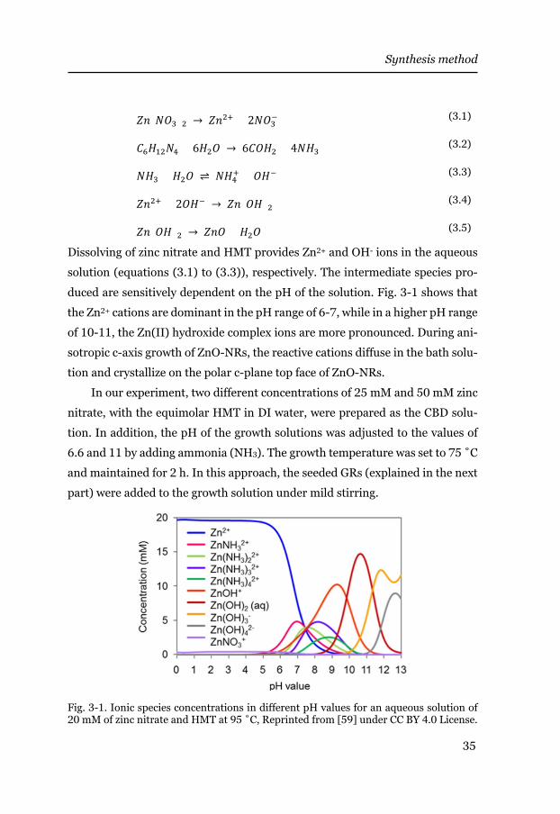
The grown ZnO-NPs on the GR have two distinguished applications in our
research. In the first application, the NPs played a seed layer role to assist the
ZnO-NRs growth on the GR nanoplates in subsequent steps. Seeding the GR by
NPs improves the GR hydrophobicity and will enhance the attachment between
the GR and the ZnO-NRs. For this aim, a low NPs surface density was synthe-
sized using a 500 mg/L dispersion of GR, a 5 mM solution of zinc acetate and
25 mM KOH. An SEM image in Fig. 3-2 shows typical seeded GRs with low-
density NPs.
Fig. 3-2. SEM image of the GRs seeded with ZnO-NPs. Reprinted from Paper I [60].
Synthesis method
37
In the other application, an optimized photocatalyst, with a high ZnO-to-GR
weight ratio of 99:1, was fabricated. A 10 mg/L dispersion of GR powder, a 10
mM and 50 mM aqueous solution of zinc acetate and KOH, respectively, were
used to synthesize the nanocomposite. The NPs here act as photogenerator of
charge carriers by absorbing UV light and producing electron-hole pairs.
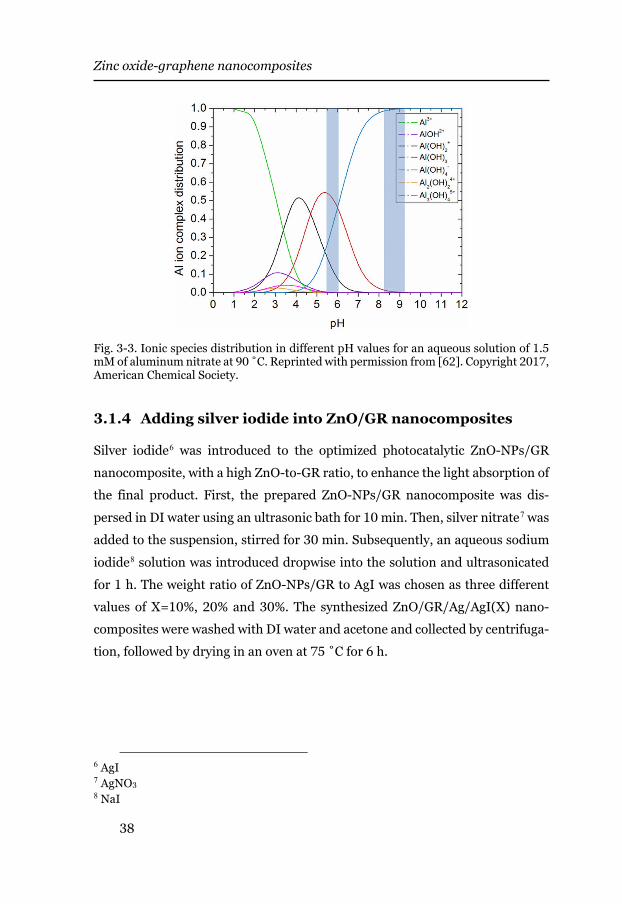
3.1.3 Aluminum doping in ZnO
The Al-doped samples were synthesized by introducing a specific amount of alu-
minum nitrate5 into the growth solution. Dissolving the Al nitrate provides dif-
ferent Al(III) hydroxide complex species in the solution with a strong depend-
ency on the solution’s pH value. As shown in Fig. 3-3, the Al(OH)3 and anion
Al(OH)4- species are dominant at pH ranges of 6-7 and 10-11, respectively.
The amount of added Al nitrate was selected in a way that the final concen-
tration of 2 mM in the growth solution was met. It is essential to stir the solution
for enough time before adding it to the growth solution. The aluminum nitrate
solution is a weak acid, reducing the pH of the growth solution to a range of 5-
5.5. This pH range is too low for the ZnO growth, and it can also dissolve the
seed layer. Before adding the seeded GRs into the growth solution, the pH of the
growth solution should be adjusted to desired values by adding enough ammo-
nia.
The Al-doping of the ZnO-NPs was performed differently by immersing a
pure piece of Al in the seed solution. The seed solution, explained in the previous
part, has a high pH value of 13 that guarantees partial dissolution of the Al and
the desired doping level of the ZnO-NPs [61].
5 Al(NO3)3.9H2O
Zinc oxide-graphene nanocomposites
38
Fig. 3-3. Ionic species distribution in different pH values for an aqueous solution of 1.5 mM of aluminum nitrate at 90 C. Reprinted with permission from [62]. Copyright 2017, American Chemical Society.
3.1.4 Adding silver iodide into ZnO/GR nanocomposites
Silver iodide6 was introduced to the optimized photocatalytic ZnO-NPs/GR
nanocomposite, with a high ZnO-to-GR ratio, to enhance the light absorption of
the final product. First, the prepared ZnO-NPs/GR nanocomposite was dis-
persed in DI water using an ultrasonic bath for 10 min. Then, silver nitrate7 was
added to the suspension, stirred for 30 min. Subsequently, an aqueous sodium
iodide8 solution was introduced dropwise into the solution and ultrasonicated
for 1 h. The weight ratio of ZnO-NPs/GR to AgI was chosen as three different
values of X=10%, 20% and 30%. The synthesized ZnO/GR/Ag/AgI(X) nano-
composites were washed with DI water and acetone and collected by centrifuga-
tion, followed by drying in an oven at 75 ˚C for 6 h.
6 AgI 7 AgNO3 8 NaI
Characterization methods
39
3.2 Characterization methods
The synthesized nanocomposites were analyzed using a large variety of experi-
mental techniques. In this part, a brief description of the characterization tech-
niques used in this thesis work is given. It can help the readers to understand
better and interpret the results.
3.2.1 Electron microscopy
Field emission scanning electron microscopy (FE-SEM) and transmission elec-
tron microscopy (TEM) were used to study the structure and the morphology of
the synthesized nanocomposites. In contrast to optical microscopes, electron
microscopes use a focused electrons beam, with a relatively much shorter elec-
tron de Broglie wavelength than photons, to produce higher magnifications.
The Zeiss Sigma 500 Gemini microscope, equipped with a field emission
gun operating at 10 kV and Gemini Inlens secondary electron detector, was used
to capture the SEM images. In SEM analysis, since the scattered electrons are
detected on the same side as the incident beam, having enough conductivity in
the samples for discharging is the only criterion to measure the specimens.
In TEM, electrons pass through the sample and the scattered beam is de-
tected on the other side of the sample. Thus, the samples should be thin enough
(<100 nm) to be electron transparent. This usually means more sample prepa-
ration steps are required for TEM measurement. The FEI Titan3 60-300 micro-
scope, equipped with image and probe Cs correctors and a monochromated high
brightness XFEG gun, operated at 300 kV, was used for TEM imaging, scanning
TEM (STEM) and high-angle annular dark-field imaging (HAADF).
Interaction between the incident electron beam in SEM and TEM and the
subshell electrons in the sample atoms leads to X-ray emission, with a charac-
teristic fingerprint of the specific elements in the sample. This method, called
dispersive x-ray spectroscopy (EDS), was used to identify the elements’ spatial
distribution and perform chemical analysis of the sample. Using STEM-EDS,
elemental map images with a resolution of a few nanometers can be obtained.
Zinc oxide-graphene nanocomposites
40
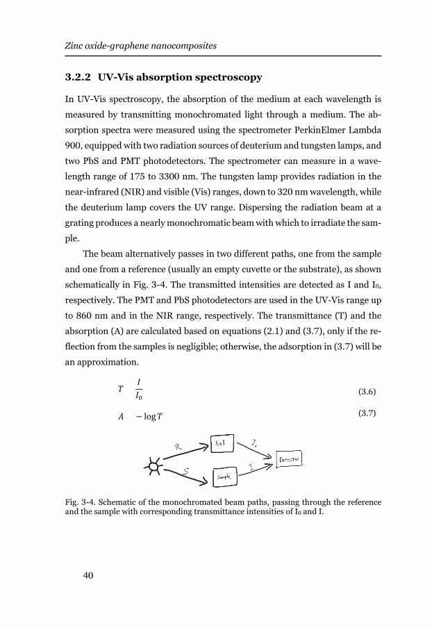
3 . 2 . 2 U V -V is absorption spectroscopy
In UV-Vis spectroscopy, the absorption of the medium at each wavelength is
measured by transmitting monochromated light through a medium. The ab-
sorption spectra were measured using the spectrometer PerkinElmer Lambda
900, equipped with two radiation sources of deuterium and tungsten lamps, and
two PbS and PMT photodetectors. The spectrometer can measure in a wave-
length range of 175 to 3300 nm. The tungsten lamp provides radiation in the
near-infrared (NIR) and visible (Vis) ranges, down to 320 nm wavelength, while
the deuterium lamp covers the UV range. Dispersing the radiation beam at a
grating produces a nearly monochromatic beam with which to irradiate the sam-
ple.
The beam alternatively passes in two different paths, one from the sample
and one from a reference (usually an empty cuvette or the substrate), as shown
schematically in Fig. 3-4. The transmitted intensities are detected as I and I0,
respectively. The PMT and PbS photodetectors are used in the UV-Vis range up
to 860 nm and in the NIR range, respectively. The transmittance (T) and the
absorption (A) are calculated based on equations (2.1) and (3.7), only if the re-
flection from the samples is negligible; otherwise, the adsorption in (3.7) will be
an approximation.
𝑇𝑇 =
𝐼𝐼𝐼𝐼0
(3.6)
𝐴𝐴 = − log𝑇𝑇 (3.7)
Fig. 3-4. Schematic of the monochromated beam paths, passing through the reference and the sample with corresponding transmittance intensities of I0 and I.
Characterization methods
41
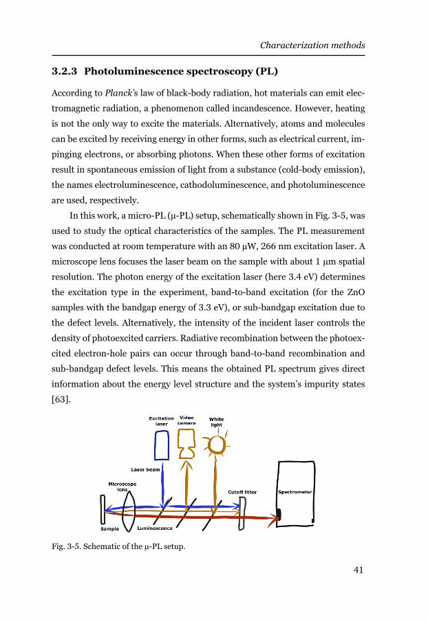
3 . 2 . 3 Photolum inescence spectroscopy ( PL)
According to Planck’s law of black-body radiation, hot materials can emit elec-
tromagnetic radiation, a phenomenon called incandescence. However, heating
is not the only way to excite the materials. Alternatively, atoms and molecules
can be excited by receiving energy in other forms, such as electrical current, im-
pinging electrons, or absorbing photons. When these other forms of excitation
result in spontaneous emission of light from a substance (cold-body emission),
the names electroluminescence, cathodoluminescence, and photoluminescence
are used, respectively.
In this work, a micro-PL (µ-PL) setup, schematically shown in Fig. 3-5, was
used to study the optical characteristics of the samples. The PL measurement
was conducted at room temperature with an 80 µW, 266 nm excitation laser. A
microscope lens focuses the laser beam on the sample with about 1 µm spatial
resolution. The photon energy of the excitation laser (here 3.4 eV) determines
the excitation type in the experiment, band-to-band excitation (for the ZnO
samples with the bandgap energy of 3.3 eV), or sub-bandgap excitation due to
the defect levels. Alternatively, the intensity of the incident laser controls the
density of photoexcited carriers. Radiative recombination between the photoex-
cited electron-hole pairs can occur through band-to-band recombination and
sub-bandgap defect levels. This means the obtained PL spectrum gives direct
information about the energy level structure and the system’s impurity states
[63].
Fig. 3-5. Schematic of the µ-PL setup.
Zinc oxide-graphene nanocomposites
42
3.2.4 Cathodoluminescence spectroscopy
Very similar to PL, cathodoluminescence uses a focused electron beam to excite
the sample locally. Then the luminescence is recorded as a spectrum. With a
spatial resolution of tens of nanometers, this technique is relatively more local
probing compared to µ-PL. One difference between PL and cathodolumines-
cence is the lower penetration depth of electrons into the substance compared
to photons. This leads to more surface-related data in cathodoluminescence
compared to bulk-related PL measurement. The cathodoluminescence study
was performed in a dedicated SEM at room temperature, operated at 5 kV. In
this thesis, the acronym CL, often used for cathodoluminescence, is reserved for
colloidal lithography, as described in the next chapter.
3.2.5 X-ray diffraction analysis (XRD)
X-ray diffraction is a form of scattering from a periodic array with long-range
order that ensures constructive interference at specific angles and so forms dif-
fraction patterns. The diffraction pattern contains information about the atomic
arrangement, the crystal plane orientation, and the element’s fingerprint. The
constructive interference angles from the parallel planes of a crystalline struc-
ture are calculated according to Bragg’s law.
In this work, we used the PANalytical X’Pert Pro diffractometer, equipped
with the Empyrean Cu X-ray tube, operating at 45 kV and an electron current of
40 mA, with the X-ray emission at the Cu Kα line with 1.5418740 Å wavelength.
An X’Celerator detector, in scanning line operation mode, and a nickel β-filter
were used on the diffracted beam side.
3.2.6 X-ray photoelectron spectroscopy (XPS)
XPS is a photoelectric experiment in which a sample is irradiated with mono-
chromatic X-ray, with a photon energy higher than the work function (φ0) of the
sample, causing emission of electrons (so-called photoelectrons) from the sam-
ple. The kinetic energy (EK) of the emitted electrons is measured by a spectrom-
eter in ultra-high vacuum (UHV) conditions. Knowing EK, the binding energy
Characterization methods
43
(EB) of the electrons in the material can be calculated according to Einstein’s
equation (3.8).
𝐸𝐸𝐾𝐾 = ℎ𝜈𝜈 − 𝐸𝐸𝐵𝐵 (3.8)
EB is defined as the energy difference between the total ground state energy of
an atom and the total energy of a cation with a core hole. In contrast to the va-
lence electrons, the core-level electrons are tightly bound to the nucleus in an
atom and do not participate in chemical reactions. In XPS, only the core-level
electrons, with an EB smaller than the energy of the X-ray source, are probed.
This detectable EB range is 0-1200 eV for a typical Al Kα X-ray source. In the
XPS spectra, each element in the sample shows a unique set of binding energies
as a fingerprint, denoted by its relevant quantum energy level (n), the angular
momentum quantum number (l), and the total angular momentum number
(j=l±s) (s is the spin quantum number).
Because of the short inelastic mean free path of electrons in materials, XPS
analysis is extremely surface sensitive, with the highest conveyed information
from a depth of a few atomic layers and a small fraction from deeper layers. The
technique has a relatively low lateral resolution, about 150 nm to 15 µm, but an
excellent detection limit of about 0.1 at% for essentially all elements except hy-
drogen.
One important application of XPS is to analyze chemical bonding in com-
plex samples, e.g., nanocomposites, by precisely determining the chemical shifts
in the EB of the core electrons. Although the core-level electrons are not involved
in chemical reactions, the electronegativity of the neighboring atoms can shift
their binding energy. In general, a lower charge density around an atom shifts
the EB of the core electrons toward higher energies.
3.2.7 Surface resistivity measurements
The surface resistivity was measured by the four-point probe method using a
Keithley 4200-SCS semiconductor characterization system. The method is
based on an in-line four-point array of probes, touching the sample surface with
an equal distance (s) from each other. A current (I) passes from the outer probes
Zinc oxide-graphene nanocomposites
44
while the potential difference between the inner probes (V) is measured. For an
infinite sample with infinitesimal thickness, the sheet resistivity (ρs) is calcu-
lated based on (3.9). For finite samples with finite thickness, depending on the
ratio of the sample dimensions to the probe spacing (d/s) and the ratio of the
sample thickness to the probe spacing (w/s), different correction factors (C) are
required. A table of the corresponding correction factors can be found in [64].
𝜌𝜌𝑠𝑠 =𝑉𝑉𝐼𝐼𝜋𝜋
ln 2=𝑉𝑉𝐼𝐼𝐶𝐶, 𝐶𝐶 ≅ 4.5324 (3.9)
3.2.8 Photoconductivity measurements
The conductivity (σ) of a substance is the product of the carrier density (n) and
the carrier mobility (µq) in the substance, according to (3.10), where q is the
elementary charge. In semiconductors, increasing the carrier density by any
form of excitation in the material, e.g., photoexcitation, leads to enhancing its
conductivity (so-called photoconductivity).
𝜎𝜎 = 𝑍𝑍. 𝑞𝑞. 𝜇𝜇𝑞𝑞 (3.10)
To measure the photoconductivity (PC) of the synthesized nanocomposites, the
materials were sandwiched between two ITO electrodes with specified area and
spacing to form an ITO/nanocomposite/ITO structure. A pulsed monochro-
matic excitation light, at room temperature and bias of 1 V, irradiated the sam-
ples. A Keithley 2400 SourceMeter recorded the current during optical excita-
tion with different wavelengths from 320 to 400 nm.
Using the decay curve in the PC, after switching off the excitation light, the
time-dependence of the PC of the samples can be calculated. The PC is propor-
tional to the density of photoelectrons in the conduction band (CB), and it de-
cays exponentially with time due to recombination of the photogenerated carri-
ers [65]. The equations below relate the PC variation rate to the photoelectron
lifetime, where σph is the photoconductivity after subtracting the dark conduc-
tivity, τd is the decay time constant (photoelectron lifetime) and σ0 is the ob-
served PC directly after switching off the light.
Characterization methods
45
𝑑𝑑𝜎𝜎𝑝𝑝ℎ𝑑𝑑𝑑𝑑
= −𝜎𝜎𝑝𝑝ℎ𝜏𝜏𝑑𝑑
(3.11)
𝐿𝐿𝑍𝑍 𝜎𝜎𝑝𝑝ℎ = −
𝑑𝑑𝜏𝜏𝑑𝑑
+ 𝐿𝐿𝑍𝑍 𝜎𝜎0 (3.12)
3.2.9 Photodegradation efficiency measurements
The photodegradation efficiency of the nanocomposites, which were developed
for photocatalysis applications, was investigated by the degradation of Congo
red (CR) dye under simulated solar light. A small amount of the nanocomposite
(50 mg) was mixed with 100 ml of CR-dye solution with an initial concentration
of 20 mg/l. After reaching the adsorption-desorption equilibrium conditions be-
tween the nanocomposite and the dye molecules in the dark, the mixture was
exposed to the simulated solar light for 60 min in 15 min interval steps. Time-
resolved UV-Vis absorption spectra of the remaining CR-dye were recorded at
each step. The CR-dye has a specific adsorption peak at 497 nm, which decays
with irradiation time, verifying the degradation of the CR-dye.
The photodegradation efficiency was calculated based on the Beer-Lambert
law, stating that the absorption is proportional to the dye concentration [66],
using equation (3.13), where A0 is the initial absorption, and A is the absorption
after irradiation.
𝐷𝐷𝑒𝑒𝐷𝐷𝐷𝐷𝐷𝐷𝑑𝑑𝐷𝐷𝑑𝑑𝐷𝐷𝐷𝐷𝑍𝑍 (%) =
𝐴𝐴0 − 𝐴𝐴𝐴𝐴0
× 100 (3.13)
In addition, the degradation rate constant was also calculated based on the
Langmuir-Hinshelwood’s pseudo-first-order kinetic model [67]. It was achieved
by linear fitting to the logarithm scale plot of the relative concentration of CR-
dye vs. time, according to the equation below: C0 is the initial concentration of
dye and C(t) is the concentration of the dye after irradiation time t.
𝐷𝐷𝑒𝑒𝐷𝐷𝐷𝐷𝐷𝐷𝑑𝑑𝐷𝐷𝑑𝑑𝐷𝐷𝐷𝐷𝑍𝑍 𝐷𝐷𝐷𝐷𝑑𝑑𝑒𝑒 𝑐𝑐𝐷𝐷𝑍𝑍𝑐𝑐𝑑𝑑𝐷𝐷𝑍𝑍𝑑𝑑 =𝐿𝐿𝑍𝑍 � 𝐶𝐶0
𝐶𝐶(𝑑𝑑)�
𝑑𝑑 (3.14)
Zinc oxide-graphene nanocomposites
46
3.3 ZnO-NRs/GR for electronics applications
The ZnO-NRs/GR nanocomposite was developed and assessed for higher elec-
trical conductivity. At the beginning of this research project, the ambition was
to fabricate conductive nanocomposites based on ZnO and GR for 3D-printed
electronics. The advantages of such a composite stem from its high macroporos-
ity, thermal and mechanical stability and cost-effectiveness, suitable for bulk
printing applications. Many electronic components can be produced by additive
manufacturing in the case of existing highly conductive and inexpensive printa-
ble materials. Here, we report the electrical and optical properties of our devel-
oped ZnO-NRs/GR nanocomposite and the effect of morphology and Al-doping
on the properties of the final nanocomposites. This section is addressed in
Paper I.
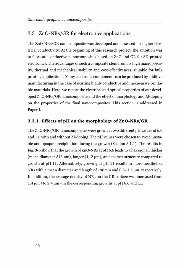
3.3.1 Effects of pH on the morphology of ZnO-NRs/GR
The ZnO-NRs/GR nanocomposites were grown at two different pH values of 6.6
and 11, with and without Al-doping. The pH values were chosen to avoid unsta-
ble and opaque precipitation during the growth (Section 3.1.1). The results in
Fig. 3-6 show that the growth of ZnO-NRs at pH 6.6 leads to a hexagonal, thicker
(mean diameter 313 nm), longer (1–2 µm), and sparser structure compared to
growth at pH 11. Alternatively, growing at pH 11 results in more needle-like
NRs with a mean diameter and length of 196 nm and 0.5–1.5 µm, respectively.
In addition, the average density of NRs on the GR surface was increased from
1.4 µm-2 to 2.4 µm-2 in the corresponding growths at pH 6.6 and 11.
ZnO-NRs/GR for electronics applications
47
Fig. 3-6. SEM images of ZnO-NRs/GR nanocomposites grown at (a) pH 6.6 and (b) pH 11. The insets show the size distribution of the NR diameter. Reprinted from Paper I [60].
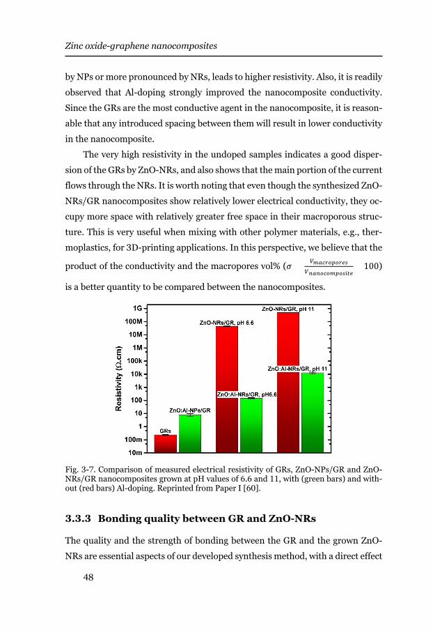
3 . 3 . 2 I m prov ing the conductiv ity of ZnO-NRs/GR by Al-dop-
ing
It is expected that the growth of wide bandgap ZnO-NRs on GR will reduce the
conductivity of the composite. To solve this issue, we degenerately doped the
ZnO-NRs by 0.5-1.5 at% Al, as explained above in Section 3.1.3. Subsequently,
the electrical resistivity of the samples was measured by the four-point probe
technique on the deposited materials. A comparison of the measured resistivi-
ties is demonstrated in Fig. 3-7. It shows that spacing between the GRs, either
Zinc oxide-graphene nanocomposites
48
by NPs or more pronounced by NRs, leads to higher resistivity. Also, it is readily
observed that Al-doping strongly improved the nanocomposite conductivity.
Since the GRs are the most conductive agent in the nanocomposite, it is reason-
able that any introduced spacing between them will result in lower conductivity
in the nanocomposite.
The very high resistivity in the undoped samples indicates a good disper-
sion of the GRs by ZnO-NRs, and also shows that the main portion of the current
flows through the NRs. It is worth noting that even though the synthesized ZnO-
NRs/GR nanocomposites show relatively lower electrical conductivity, they oc-
cupy more space with relatively greater free space in their macroporous struc-
ture. This is very useful when mixing with other polymer materials, e.g., ther-
moplastics, for 3D-printing applications. In this perspective, we believe that the
product of the conductivity and the macropores vol% (𝜎𝜎 × 𝑉𝑉𝑚𝑚𝑚𝑚𝑐𝑐𝑐𝑐𝑐𝑐𝑐𝑐𝑐𝑐𝑐𝑐𝑐𝑐𝑐𝑐
𝑉𝑉𝑛𝑛𝑚𝑚𝑛𝑛𝑐𝑐𝑐𝑐𝑐𝑐𝑚𝑚𝑐𝑐𝑐𝑐𝑐𝑐𝑛𝑛𝑛𝑛𝑐𝑐× 100)
is a better quantity to be compared between the nanocomposites.
Fig. 3-7. Comparison of measured electrical resistivity of GRs, ZnO-NPs/GR and ZnO-NRs/GR nanocomposites grown at pH values of 6.6 and 11, with (green bars) and with-out (red bars) Al-doping. Reprinted from Paper I [60].
3.3.3 Bonding quality between GR and ZnO-NRs
The quality and the strength of bonding between the GR and the grown ZnO-
NRs are essential aspects of our developed synthesis method, with a direct effect
ZnO-NRs/GR for electronics applications
49
on the composite conductivity and its optical properties. The time-dependent
UV-Vis spectroscopy reveals the existence of different material phases in the
dispersion of the nanocomposite. The separate phases in the dispersion precip-
itate with different speeds, and consequently, can be identified using their dif-
ferent absorption spectra. Our results in Paper I show a uniform decrease in ab-
sorption for the ZnO-NRs/GR nanocomposites grown at higher pH values 11
and a non-uniform change for the samples grown at pH 6.6. This suggests that
the growth at a higher pH solution leads to a better attachment of ZnO-NRs to
the GRs.
3.3.4 Optical properties of ZnO/GR nanocomposites
The effect of the pH growth solution and Al-doping on the optical properties of
the ZnO/GR nanocomposites was studied by PL analysis. In Paper I, the PL data
show variation in the near-bandedge emission (NBE) in the UV range, and deep-
level emission (DLE) in the visible spectrum for the various nanocomposites.
Table 3-1 shows the ratio of NBE-to-DLE integrated intensities (INBE/IDLE) for
different ZnO-NRs nanocomposites.
To summarize, growing at higher pH 11 caused a significantly lower UV-to-
visible emission ratio in all the samples. This lower emission ratio indicates
higher defect levels concentration in the samples grown at pH 11, due to the
increased surface-to-volume ratio in the structure compared to growing at pH
6.6. It was also observed that Al-doping reduced the INBE/IDLE ratio for all sam-
ples. This reduction can be explained by the introduced Al donor levels in the
bandgap and by the lower crystalline quality of the doped ZnO [68, 69].
The results also show an increase in UV-to-visible emission ratio for
ZnO/GR composite samples compared to the pure ZnO structures. Reviewing
the literature, this increase in the emission ratio can be attributed to the reduc-
tion of the surface defects concentration of the ZnO by the oxygen groups on the
GR surface, or to resonant excitation of GR plasmons. More information can be
found in Paper I.
Zinc oxide-graphene nanocomposites
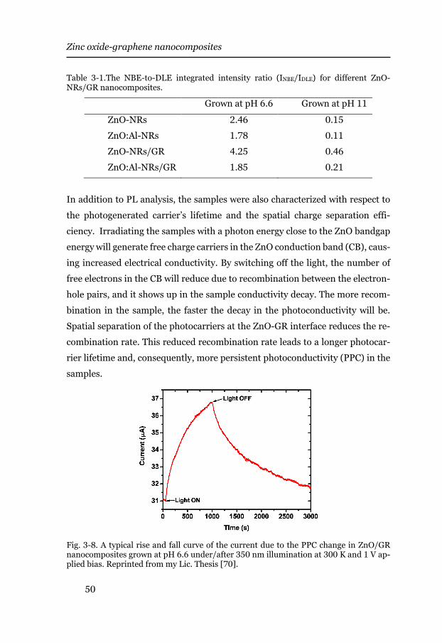
50
Table 3-1.The NBE-to-DLE integrated intensity ratio (INBE/IDLE) for different ZnO-NRs/GR nanocomposites.
Grown at pH 6.6 Grown at pH 11
ZnO-NRs 2.46 0.15
ZnO:Al-NRs 1.78 0.11
ZnO-NRs/GR 4.25 0.46
ZnO:Al-NRs/GR 1.85 0.21
In addition to PL analysis, the samples were also characterized with respect to
the photogenerated carrier’s lifetime and the spatial charge separation effi-
ciency. Irradiating the samples with a photon energy close to the ZnO bandgap
energy will generate free charge carriers in the ZnO conduction band (CB), caus-
ing increased electrical conductivity. By switching off the light, the number of
free electrons in the CB will reduce due to recombination between the electron-
hole pairs, and it shows up in the sample conductivity decay. The more recom-
bination in the sample, the faster the decay in the photoconductivity will be.
Spatial separation of the photocarriers at the ZnO-GR interface reduces the re-
combination rate. This reduced recombination rate leads to a longer photocar-
rier lifetime and, consequently, more persistent photoconductivity (PPC) in the
samples.
Fig. 3-8. A typical rise and fall curve of the current due to the PPC change in ZnO/GR nanocomposites grown at pH 6.6 under/after 350 nm illumination at 300 K and 1 V ap-plied bias. Reprinted from my Lic. Thesis [70].
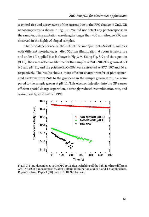
ZnO-NRs/GR for electronics applications
51
A typical rise and decay curve of the current due to the PPC change in ZnO/GR
nanocomposites is shown in Fig. 3-8. We did not detect any photoresponse in
the samples, using excitation wavelengths longer than 400 nm. Also, no PPC was
observed in the highly Al-doped samples.
The time-dependence of the PPC of the undoped ZnO-NRs/GR samples
with different morphologies, after 350 nm illumination at room temperature
and under 1 V applied bias is shown in Fig. 3-9. Using Fig. 3-9 and the equation
(3.12), the excess electron lifetime for the samples of ZnO-NRs/GR grown at pH
6.6 and pH 11, and the pristine ZnO-NRs were extracted as 877, 107 and 56 s,
respectively. The results show a more efficient charge transfer of photogener-
ated electrons from ZnO to the graphene in the sample grown at pH 6.6 com-
pared to the sample grown at pH 11. This electron injection into the GR causes
efficient spatial charge separation, a strongly reduced recombination rate, and
consequently, an enhanced PPC.
Fig. 3-9. Time-dependence of the PPC (σph) after switching off the light for three different ZnO-NRs/GR nanocomposites, after 350 nm illumination at 300 K and 1 V applied bias. Reprinted from Paper I [60] under CC BY 3.0 License.
Zinc oxide-graphene nanocomposites
52
3.4 ZnO-NPs/GR for photocatalytic applications
Our last PPC results inspired us to use the developed ZnO/GR nanocomposite
for photocatalytic applications, an area where the charge separation phenomena
and the photocarrier’s lifetime are of great importance. In this application, the
charge separation interfaces are more important than the bulk of the materials.
For this reason, the nanoparticle form of ZnO, instead of NRs, was chosen to
increase the ZnO-GR interfaces. In addition, the weight ratio of ZnO to Gr was
increased to 99:1, as the primary light absorption material in the nanocompo-
site.
Although the tested ZnO/GR samples showed a promising charge separa-
tion capability, they are not active in the visible light range. The large bandgap
of ZnO can only absorb incident wavelength in the UV range. This will limit the
photocatalytic efficiency of these materials under solar irradiation, with its
broad intensity peak in the visible range. To overcome this drawback, we intro-
duced different weight ratios of lower bandgap (2.8 eV) AgI-NPs into the
ZnO/GR nanocomposites. The new ZnO/GR/AgI nanocomposites were ana-
lyzed with respect to their crystallinity, morphology, chemical structure, and
photodegradation efficiency of an organic pollutant. This work is described in
Paper II.
3.4.1 Silver iodide
Narrow bandgap silver-based semiconductors, including silver oxide, silver sul-
fide and silver halides, particularly AgI, with its excellent visible light absorp-
tion, have been widely studied for photocatalysis applications [71]. Historically,
these Ag-based materials have been extensively used in photography for many
years due to their highly sensitive light decomposing behavior. They will quickly
decompose to metallic silver atoms (Ag0) when exposed to light. However, this
Ag+ to Ag0 reduction will quickly be stopped at the initial stage of the reaction
by a self-stabilizing mechanism. Clusters of reduced Ag0 atoms are formed on
the AgI-NPs, preventing further decomposition of the semiconductor [71].
Therefore, we use the Ag/AgI in our notation instead of only AgI.
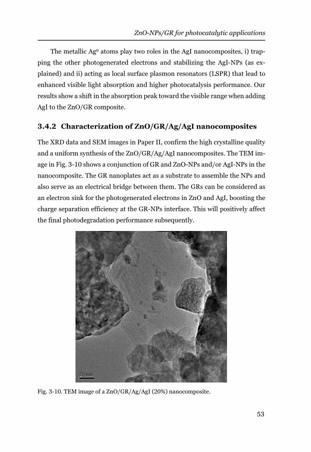
ZnO-NPs/GR for photocatalytic applications
53
The metallic Ag0 atoms play two roles in the AgI nanocomposites, i) trap-
ping the other photogenerated electrons and stabilizing the AgI-NPs (as ex-
plained) and ii) acting as local surface plasmon resonators (LSPR) that lead to
enhanced visible light absorption and higher photocatalysis performance. Our
results show a shift in the absorption peak toward the visible range when adding
AgI to the ZnO/GR composite.
3 . 4 . 2 Characteriz ation of ZnO/GR/Ag/AgI nanocom posites
The XRD data and SEM images in Paper II, confirm the high crystalline quality
and a uniform synthesis of the ZnO/GR/Ag/AgI nanocomposites. The TEM im-
age in Fig. 3-10 shows a conjunction of GR and ZnO-NPs and/or AgI-NPs in the
nanocomposite. The GR nanoplates act as a substrate to assemble the NPs and
also serve as an electrical bridge between them. The GRs can be considered as
an electron sink for the photogenerated electrons in ZnO and AgI, boosting the
charge separation efficiency at the GR-NPs interface. This will positively affect
the final photodegradation performance subsequently.
Fig. 3-10. TEM image of a ZnO/GR/Ag/AgI (20%) nanocomposite.
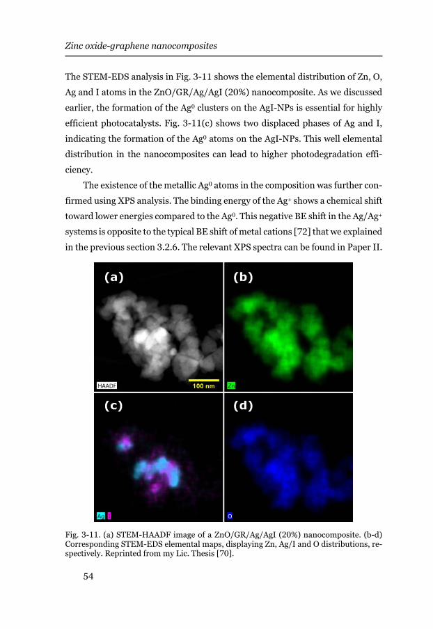
Zinc oxide-graphene nanocomposites
54
The STEM-EDS analysis in Fig. 3-11 shows the elemental distribution of Zn, O,
Ag and I atoms in the ZnO/GR/Ag/AgI (20%) nanocomposite. As we discussed
earlier, the formation of the Ag0 clusters on the AgI-NPs is essential for highly
efficient photocatalysts. Fig. 3-11(c) shows two displaced phases of Ag and I,
indicating the formation of the Ag0 atoms on the AgI-NPs. This well elemental
distribution in the nanocomposites can lead to higher photodegradation effi-
ciency.
The existence of the metallic Ag0 atoms in the composition was further con-
firmed using XPS analysis. The binding energy of the Ag+ shows a chemical shift
toward lower energies compared to the Ag0. This negative BE shift in the Ag/Ag+
systems is opposite to the typical BE shift of metal cations [72] that we explained
in the previous section 3.2.6. The relevant XPS spectra can be found in Paper II.
Fig. 3-11. (a) STEM-HAADF image of a ZnO/GR/Ag/AgI (20%) nanocomposite. (b-d) Corresponding STEM-EDS elemental maps, displaying Zn, Ag/I and O distributions, re-spectively. Reprinted from my Lic. Thesis [70].
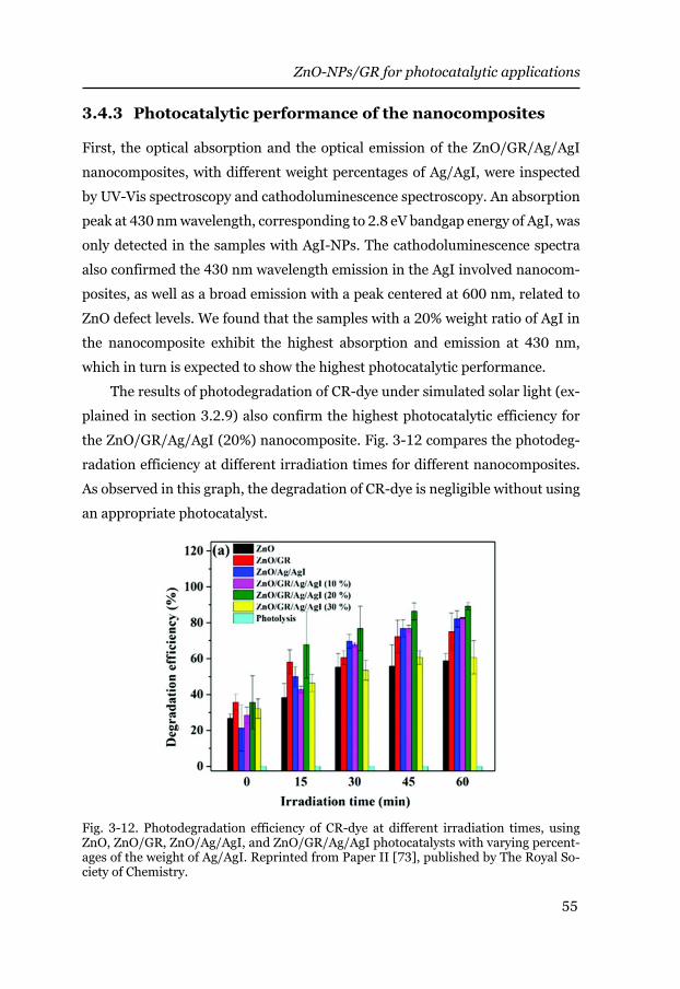
ZnO-NPs/GR for photocatalytic applications
55
3 . 4 . 3 Photocatalytic perform ance of the nanocom posites
First, the optical absorption and the optical emission of the ZnO/GR/Ag/AgI
nanocomposites, with different weight percentages of Ag/AgI, were inspected
by UV-Vis spectroscopy and cathodoluminescence spectroscopy. An absorption
peak at 430 nm wavelength, corresponding to 2.8 eV bandgap energy of AgI, was
only detected in the samples with AgI-NPs. The cathodoluminescence spectra
also confirmed the 430 nm wavelength emission in the AgI involved nanocom-
posites, as well as a broad emission with a peak centered at 600 nm, related to
ZnO defect levels. We found that the samples with a 20% weight ratio of AgI in
the nanocomposite exhibit the highest absorption and emission at 430 nm,
which in turn is expected to show the highest photocatalytic performance.
The results of photodegradation of CR-dye under simulated solar light (ex-
plained in section 3.2.9) also confirm the highest photocatalytic efficiency for
the ZnO/GR/Ag/AgI (20%) nanocomposite. Fig. 3-12 compares the photodeg-
radation efficiency at different irradiation times for different nanocomposites.
As observed in this graph, the degradation of CR-dye is negligible without using
an appropriate photocatalyst.
Fig. 3-12. Photodegradation efficiency of CR-dye at different irradiation times, using ZnO, ZnO/GR, ZnO/Ag/AgI, and ZnO/GR/Ag/AgI photocatalysts with varying percent-ages of the weight of Ag/AgI. Reprinted from Paper II [73], published by The Royal So-ciety of Chemistry.

Zinc oxide-graphene nanocomposites
56
A proposed photodegradation mechanism, including the energy band structure,
can be found in Paper II. Briefly described, both ZnO and AgI absorb light at
different wavelengths and generate electrons and holes in their conduction band
(CB) and valence band (VB). Because of the band offsets, the electrons in the CB
of AgI are transferred to CB of ZnO. The holes migrate in opposite direction,
from the VB of ZnO to the VB of AgI. This charge separation enhances the carrier
lifetime by reducing the recombination probability between the e/h pairs. Sub-
sequently, the photogenerated electrons can migrate even further to the GR,
causing strongly enhanced photocatalytic performance.
The separated electrons react with oxygen molecules to produce superoxide
and hydroxyl radicals. The organic pollutant molecules (CR-dye) are decom-
posed by reacting to these active species in the solution. In the other reaction,
the photogenerated holes can directly oxidize the adsorbed dye molecules and
decompose the organic pollutants.
57
4 Template-assisted nanofabrication of ZnO-NRs/GR
In the previous chapter, we used CBD for the synthesis of the ZnO/GR nano-
composites. Although various composites and nanostructures can be produced
by this simple and inexpensive method, the final product usually consists of ran-
dom structures, and it is hard to control their architecture and alignment. In
many applications, especially for device fabrication, it is important to be able to
control the nanostructure’s alignment, ordering, density, and growth area.
This chapter describes a completely different approach, in which vertically
aligned arrays of ZnO-NRs were grown on appropriately seeded Si wafer sub-
strates. To accurately control the NRs surface density and selectively grow the
NRs only in specific areas, colloidal lithography (CL) was employed to pattern
the substrates in a relatively simple process.
To further improve the ZnO-NRs alignment and fabricate electronic de-
vices, a graphene oxide (GO) buffer layer was introduced between the Si sub-
strate and the ZnO seed layer. This GO layer, after reduction to reduced gra-
phene oxide (rGO), served as a compensator for the crystalline lattice mismatch
between the Si and the ZnO and also as a back contact for device fabrication on
insulating substrates.
4.1 Synthesis methods
The synthesis process of the aligned ZnO-NRs is essentially the same as de-
scribed in the previous chapter. It includes seed layer preparation and ZnO-NRs
growth on the seeded layers. However, a few changes in the chemicals used and
the growth recipe were necessary to adapt the CBD technique for selective NR
growth on different substrates. First, we needed to prepare a better GR disper-
sion. The GR nanoplates in the last part were purchased commercially in powder
Template-assisted nanofabrication of ZnO-NRs/GR
58
form and dispersed in DI water using ultrasonication. The prepared GR disper-
sion was not stable enough to make uniform spray-coated layers on the sub-
strates required for this part of our research. So, we synthesized the GO using
the improved Hummer’s method, which will be explained below.
The ZnO-NP seed layer was also prepared differently by sol-gel and dip-
coating techniques. The former solution of zinc acetate and KOH used to deco-
rate the GR with ZnO-NPs, results in NP clusters and a non-uniform coating on
the substrates. Therefore, we used the sol-gel solution to deposit perfectly uni-
form ZnO thin film layers on various substrates independently. Also, the CBD
process was modified a little to achieve the highest alignment and quality of the
ZnO-NRs.
4.1.1 Synthesis of GO using the improved Hummer’s method
Graphene oxide (GO) was prepared using the improved Hummer’s method ac-
cording to the recipe described in [45]. The process is based on the chemical
exfoliation of natural graphite flakes. Two types of natural and synthetic graph-
ite are available commercially [74], and only the natural type can be used for GO
synthesis.
First, 1 g of graphite flakes (mesh -20+100, with a particle size range of 150-
850 µm) were oxidized using a mixture of concentrated sulfuric acid9 and phos-
phoric acid10 with a volume ratio of 9:1 (60:7 ml), stirring at 80 ˚C for 30 min.
The mixture cooled to room temperature, followed by 30 min ultrasonication
(Fig. 4-1(a)). Subsequently, the mixture container was moved into an ice bath at
0˚C, and 6 g of potassium permanganate11 was added to the mixture very slowly
while stirring vigorously. The reaction is extremely exothermic; thus, caution is
needed not to allow the mixture temperature to rise above 20 ˚C while adding
the KMnO4. After this, the ice bath was removed, and the mixture was stirred at
35 ˚C for 2 h. Subsequently, the mixture was diluted by adding 120 ml of DI
9 H2SO4 (98%) 10 H3PO4 (85%) 11 KMnO4
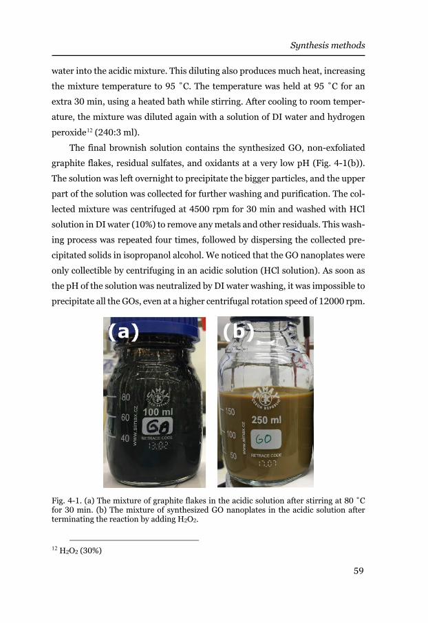
Synthesis methods
59
water into the acidic mixture. This diluting also produces much heat, increasing
the mi ture temperature to 95 ˚C. The temperature was held at 95 ˚C for an
extra 30 min, using a heated bath while stirring. After cooling to room temper-
ature, the mixture was diluted again with a solution of DI water and hydrogen
peroxide 1 2 (240:3 ml).
The final brownish solution contains the synthesized GO, non-exfoliated
graphite flakes, residual sulfates, and oxidants at a very low pH (Fig. 4-1(b)).
The solution was left overnight to precipitate the bigger particles, and the upper
part of the solution was collected for further washing and purification. The col-
lected mixture was centrifuged at 4500 rpm for 30 min and washed with HCl
solution in DI water (10%) to remove any metals and other residuals. This wash-
ing process was repeated four times, followed by dispersing the collected pre-
cipitated solids in isopropanol alcohol. We noticed that the GO nanoplates were
only collectible by centrifuging in an acidic solution (HCl solution). As soon as
the pH of the solution was neutralized by DI water washing, it was impossible to
precipitate all the GOs, even at a higher centrifugal rotation speed of 12000 rpm.
Fig. 4-1. (a) The mixture of graphite flakes in the acidic solution after stirring at 80 ˚C for 30 min. (b) The mixture of synthesized GO nanoplates in the acidic solution after terminating the reaction by adding H2O2.
1 2 H2O2 (30%)
Template-assisted nanofabrication of ZnO-NRs/GR
60
4.1.2 ZnO sol-gel solutions
The ZnO-NPs synthesis procedure discussed in the previous chapter leads to
NPs with size distribution in a range of 50-120 nm. The seed layers, produced
by the spin coating of these NPs on a substrate, showed a non-uniform island-
like coating of NPs. Although changing the growth solvent to methanol and re-
peating the spin-coating step improved the seed layer surface coverage, it was
not uniform enough for our nanofabrication process (Fig. 4-2(a)).
To improve the uniformity and the smoothness of the seed layers, a sol-gel
solution of 8.25 g of zinc acetate and 2.26 ml of monoethanolamine13 (ethano-
lamine), with an equimolar final concentration of 375 mM, in 100 ml of pure
ethanol was prepared [75, 76]. The solution was stirred at 60 ˚C for 10 h and
then at room temperature overnight. Fig. 4-2(b) shows an SEM image of a seed
layer of ZnO-NPs, deposited on a Si substrate using the sol-gel method and dip-
coating technique. Compared to the other method, the sol-gel process yields a
highly uniform and dense seed layer with almost full surface coverage.
4.1.3 CBD of ZnO-NRs on patterned substrates
The same CBD method, explained in the previous chapter, was used for growing
the ZnO-NRs, with and without Al-doping. The only change was to increase the
growth temperature from 75 ˚C to 95 ˚C. Increasing the growth temperature
causes a merging of the multiple closely packed narrow NRs into a single thicker
NR. The growth of a single NR is crucial in our novel nanofabrication method,
as will be explained below [77].
It is also worth noting that the ZnO-NRs growth is performed on substrates
in this approach, in contrast to the previous chapter. The prepared substrates
were mounted upside down in the CBD solution to prevent any precipitant fall-
ing on the growth surface. We noticed that bubbles are formed in the solution
during the experiment and may be trapped under the substrate, causing dam-
aged or un-grown areas on the substrate surface. A little tilted mounting of the
13 NH2CH2CH2OH
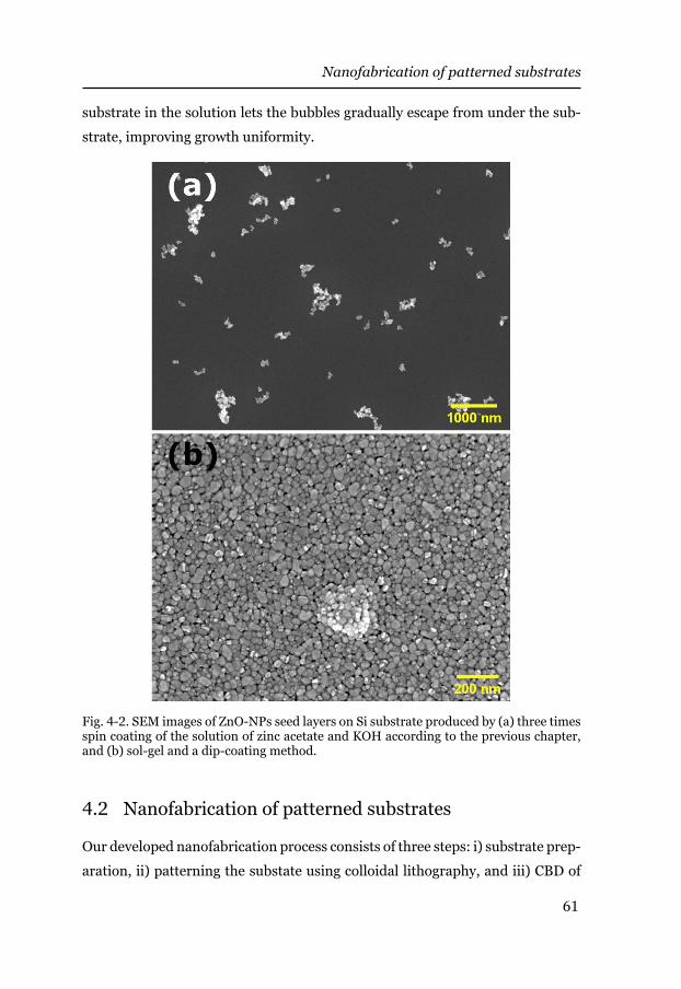
Nanofabrication of patterned substrates
61
substrate in the solution lets the bubbles gradually escape from under the sub-
strate, improving growth uniformity.
Fig. 4-2. SEM images of ZnO-NPs seed layers on Si substrate produced by (a) three times spin coating of the solution of zinc acetate and KOH according to the previous chapter, and (b) sol-gel and a dip-coating method.
4.2 Nanofabrication of patterned substrates
Our developed nanofabrication process consists of three steps: i) substrate prep-
aration, ii) patterning the substate using colloidal lithography, and iii) CBD of
Template-assisted nanofabrication of ZnO-NRs/GR
62
ZnO-NRs on the patterned substrates. Two types of Si/ZnO-NPs and
Si/GO/ZnO-NPs seeded substrates were prepared using the sol-gel solution and
a dip-coating technique. In the first structure, described in Paper III, the ZnO
seed layer was directly formed on the Si substrate. In the second structure, dis-
cussed in Paper IV, a GO layer was deposited on the Si substrate prior to the
ZnO seed layer. This GO layer serves as a buffer layer to compensate for the
crystal lattice mismatch between the Si and the ZnO, and also as a back contact
for device fabrication on insulator substrates. The CL patterning process is ba-
sically the same for both substrate preparation methods.
4.2.1 Spray coating of GO buffer layers
A dispersion of the synthesized GO in N,N-Dimethylformamide14 (DMF) with a
final concentration of 2 mg/ml was prepared by ultrasonication for 30 min. Al-
ternatively, isopropanol alcohol can also be used, although DMF results in more
uniform layers. Both solutions remained stable for more than two weeks.
We used spray coating to deposit the GO dispersion on two-inch Si wafers.
However, prior to that, the adhesion of GO to the Si substrate was enhanced by
spin coating a thin layer of Adhesion Promoter AP3000 from the Advanced Elec-
tronics Materials, containing vinyltriacetoxysilane15 in 1-Methoxy-2-propanol
solvent, at 4000 rpm for 30 s. It is critical to preheat the substrates at 120 ˚C for
5 min immediately before spin-coating to desorb surface moisture, and to per-
form soft baking at 120 ˚C for 10 min after the coating.
Subsequently, the coated Si substrate was placed on a hotplate at 120 ˚C
under a fume hood, and 20 ml of the GO solution was pulse-wise sprayed on the
sample with 1 s spraying and 3 s waiting times. An airbrush at a 10 cm distance
from the sample, operating with nitrogen carrier gas at 2 bar pressure, was used.
Fig. 4-3 shows the spray-coated GO on a Si wafer with and without substrate
silanization. The silane-coated sample survived after five cycles of tape
14 HCON(CH3)2 15 (CH3CO2)3SiCH=CH2
Nanofabrication of patterned substrates
63
stripping, while the piece without adhesion promoter was delaminated during
the liftoff process.
The thickness of the spray-coated GO layer was measured using a stylus
Dektak-3ST profilometer to be in the range of 100-150 nm. Fig. 4-4 shows a
corresponding cross-sectional SEM image of a sample.
Fig. 4-3. Spray-coated GO on Si substrate (a) with, and (b) without silanization, after five-cycles of a tape stripping test. The samples also have a PMMA coating on top that will be explained below.
Fig. 4-4. Cross-sectional SEM image of spray-coated GO on Si substrate.
Template-assisted nanofabrication of ZnO-NRs/GR
64
4.2.2 Dip-coating of the ZnO sol-gel solution
A computer-controlled dip-coater was used to dip in and pull out the substrates
into the ZnO-NPs sol-gel solution with a speed range of 10-30 mm/s at room
temperature. In this work, the dip-coating of the seed layers was carried out on
two different substrates, a bare Si wafer and the GO coated Si (Si/GO). For the
bare Si samples, the coating process was repeated twice, including an annealing
step at 300 ˚C for 10 min after each dip-coating step.
However, the Si/GO samples cannot tolerate high temperatures for a long
time because of combustion of the GO layer in air. We measured a burning rate
of 50-65 nm/min for the GO layer at 300 ˚C in air. The annealing duration was
limited only to 1 min to avoid oxidizing all the C atoms of the GO layer. In the
end, a thickness of about 85-100 nm of the GO layer remained after the anneal-
ing process.
4.2.3 Colloidal lithography (CL) patterning
A polymer resist layer was spin coated on the seeded substrate to identify the
selected growth areas on the samples. An array of nanoholes was then fabricated
in the resist layer using the CL technique. CL allows for flexibility in the fabrica-
tion process and results in low-cost nanopatterning. Among other advantages,
it is inexpensive, substrate independent, offers excellent control of the nanohole
size, and is suitable for large wafer-scale area patterning [78–80].
In this work, we used a double-layer resist of a sacrificial PMMA16 electron-
beam resist and then a positive MICROPOSIT S1805 photoresist on the seeded
substrates. Various PMMA solutions in different solvents, including toluene, an-
isole, diethyl carbonate and DMF, were tested for spin coating of the first resist
layer. Regarding the thickness and the uniformity of the layers, toluene results
in a thick uniform layer, while anisole and diethyl carbonate solvents give thin-
ner and uniform coating layers. In contrast, samples produced using DMF sol-
vent showed a non-uniform coating.
16 poly(methyl methacrylate), MW = 950k
Nanofabrication of patterned substrates
65
After coating the resist layers, 5 min UV-Ozone treatment was necessary to
improve the hydrophilicity of the resist for the following steps. A positively
charged monolayer of PDDA17 was then pipetted on the sample surface and
thoroughly rinsed with DI water after 1 min of settling. The positively charged
monolayer of PDDA will electrostatically adhere the negatively charged polysty-
rene nanobeads (PS-NBs) to the substrate in the next step. The PS-NBs adhesion
to the surface depends strongly on the number of the PDDA layers and will be
reduced by multilayer-thick PDDA layers. Rinsing the PDDA layer under DI wa-
ter flow for about 10 s improves the coated PS-NBs surface coverage.
A range of PS-NBs diameter sizes from 100 nm to 100 µm, suspended in
water, is commercially available from microParticles GmbH, Germany. In this
thesis, we used the PS-NBs with mean diameters of 107, 140 and 320 nm for
CL-patterning. Various concentrations of 0.1, 0.02, 0.01 and 0.003 wt% of the
PS-NBs suspension in DI water were prepared by ultrasonication. Subsequently,
a monolayer of PS-NBs was dispersed on the sample surface and gently rinsed
with DI water after 1 min of settling. Fig. 4-5(a) shows a schematic of the sample
at this stage.
4.2.4 Thermal evaporation
Thermal evaporation is a member of a bigger category of physical vapor deposi-
tion (PVD) techniques in which the materials are transported from a source to
the growth substrate in the vapor phase. First, a material source is evaporated
by receiving energy in various ways, including resistive heating in thermal evap-
oration, ion bombardment in sputtering, from an electron-beam in EBPVD, or
a laser beam in pulsed laser deposition (PLD). In all these cases, a high or ultra-
high vacuum is needed to i) prevent the vaporized materials and the heated parts
in the evaporator from oxidation, ii) reduce the materials’ evaporation temper-
ature, and iii) increase the mean free path of the vaporized particles, allowing
transport without intermolecular collisions.
17 poly(diallyldimethylammonium), MW = (200-350)k
Template-assisted nanofabrication of ZnO-NRs/GR
66
The vaporized particles are adsorbed on exposed surfaces inside the cham-
ber, including the substrate, and condensation of material takes place. The
thickness of the deposited materials is simultaneously monitored using a quartz
crystal microbalance (QCM) and can be controlled by the deposition time.
In this thesis, a Balzers BA 510 evaporator was used to thermally evaporate
a 30 nm thick Al layer on the samples at a high vacuum (HV) pressure of
6× 10⁻⁷ Torr (Fig. 4-5(b)). The evaporator was equipped with a diffusion pump
with 2000 l/s pumping speed and a combination of Pirani and cold cathode vac-
uum gauges to cover all the operating pressure ranges. The molten Al at high
temperature is highly corrosive to the tungsten boat, penetrating it and alloying
with the tungsten. To avoid this, the deposition rate was increased as high as
possible to about 5-10 nm/s. After Al-coating, the Al-coated PS-NBs were re-
moved by tape stripping using acrylic silicon-free Ultron 1009R tape, leaving
behind open nanoholes in the Al film (Fig. 4-5(c)).
Fig. 4-5. Schematic of the CL nanofabrication process steps. (a) A substrate coated with a ZnO-NP seed layer, a double-layer polymer resist, and dispersed PS-NBs. (b) Thermal evaporation of an Al mask. (c) Removing the Al-coated PS-NBs by tape stripping. (d) Dry etching of the resist. (e) Wet etching of the Al mask. (f) Selective ZnO-NR growth in the holes of the patterned resist template. Reprinted from Paper III [81] under CC BY 4.0 License.
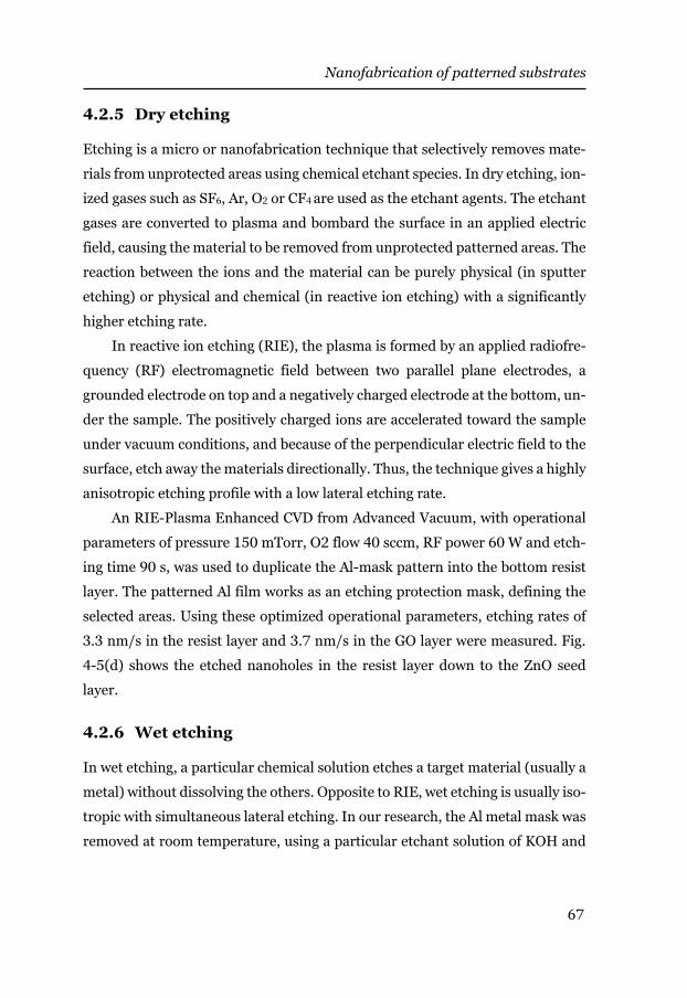
Nanofabrication of patterned substrates
67
4.2.5 Dry etching
Etching is a micro or nanofabrication technique that selectively removes mate-
rials from unprotected areas using chemical etchant species. In dry etching, ion-
ized gases such as SF6, Ar, O2 or CF4 are used as the etchant agents. The etchant
gases are converted to plasma and bombard the surface in an applied electric
field, causing the material to be removed from unprotected patterned areas. The
reaction between the ions and the material can be purely physical (in sputter
etching) or physical and chemical (in reactive ion etching) with a significantly
higher etching rate.
In reactive ion etching (RIE), the plasma is formed by an applied radiofre-
quency (RF) electromagnetic field between two parallel plane electrodes, a
grounded electrode on top and a negatively charged electrode at the bottom, un-
der the sample. The positively charged ions are accelerated toward the sample
under vacuum conditions, and because of the perpendicular electric field to the
surface, etch away the materials directionally. Thus, the technique gives a highly
anisotropic etching profile with a low lateral etching rate.
An RIE-Plasma Enhanced CVD from Advanced Vacuum, with operational
parameters of pressure 150 mTorr, O2 flow 40 sccm, RF power 60 W and etch-
ing time 90 s, was used to duplicate the Al-mask pattern into the bottom resist
layer. The patterned Al film works as an etching protection mask, defining the
selected areas. Using these optimized operational parameters, etching rates of
3.3 nm/s in the resist layer and 3.7 nm/s in the GO layer were measured. Fig.
4-5(d) shows the etched nanoholes in the resist layer down to the ZnO seed
layer.
4.2.6 Wet etching
In wet etching, a particular chemical solution etches a target material (usually a
metal) without dissolving the others. Opposite to RIE, wet etching is usually iso-
tropic with simultaneous lateral etching. In our research, the Al metal mask was
removed at room temperature, using a particular etchant solution of KOH and
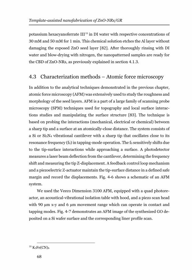
Template-assisted nanofabrication of ZnO-NRs/GR
68
potassium hexacyanoferrate III18 in DI water with respective concentrations of
30 mM and 50 mM for 1 min. This chemical solution etches the Al layer without
damaging the exposed ZnO seed layer [82]. After thoroughly rinsing with DI
water and blow-drying with nitrogen, the nanopatterned samples are ready for
the CBD of ZnO-NRs, as previously explained in section 4.1.3.
4.3 Characterization methods – Atomic force microscopy
In addition to the analytical techniques demonstrated in the previous chapter,
atomic force microscopy (AFM) was extensively used to study the roughness and
morphology of the seed layers. AFM is a part of a large family of scanning probe
microscopy (SPM) techniques used for topography and local surface interac-
tions studies and manipulating the surface structure [83]. The technique is
based on probing the interactions (mechanical, electrical or chemical) between
a sharp tip and a surface at an atomically-close distance. The system consists of
a Si or Si3N4 vibrational cantilever with a sharp tip that oscillates close to its
resonance frequency (f0) in tapping-mode operation. The f0 sensitively shifts due
to the tip-surface interactions while approaching a surface. A photodetector
measures a laser beam deflection from the cantilever, determining the frequency
shift and measuring the tip Z-displacement. A feedback control loop mechanism
and a piezoelectric Z-actuator maintain the tip-surface distance in a defined safe
margin and record the displacements. Fig. 4-6 shows a schematic of an AFM
system.
We used the Veeco Dimension 3100 AFM, equipped with a quad photore-
actor, an acoustical-vibrational isolation table with hood, and a piezo scan head
with 90 µm x-y and 6 µm movement range which can operate in contact and
tapping modes. Fig. 4-7 demonstrates an AFM image of the synthesized GO de-
posited on a Si wafer surface and the corresponding liner profile scan.
18 K3Fe(CN)6
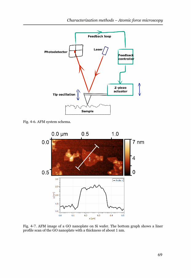
Characterization methods – Atomic force microscopy
69
Fig. 4-6. AFM system schema.
Fig. 4-7. AFM image of a GO nanoplate on Si wafer. The bottom graph shows a liner profile scan of the GO nanoplate with a thickness of about 1 nm.
Template-assisted nanofabrication of ZnO-NRs/GR
70
4.4 Characterization of the CL-patterned substrates
A full detailed characterization of the CL-patterned substrates has been reported
in Paper III and IV. Here, more detailed information is provided to fill the gap
between these two works and connect them logically.
4.4.1 Why using Si/GO substrates?
The CL method was tested on different substrates, including fluorine-doped tin
oxide (FTO) and Ti and Au-coated glass substrates. An electrically conductive
substrate is required to make a device. The other requirement is the stability of
the substrate during the fabrication process. On the other hand, growing on Si
has the significant advantage of being integrated with the well-developed Si in-
dustry.
Testing the CL on FTO substrates was not very successful due to the rela-
tively high surface roughness of the FTO. High points on the surface apexes are
usually exposed through the resist layer before etching, and depths are rarely
accessible through the patterned nanoholes. A cross-section SEM image of a typ-
ical CL-patterned resist layer on an FTO substrate is shown in Fig. 4-8.
Fig. 4-8. Cross-sectional SEM image of the CL-patterned resist layer on FTO surface be-fore wet-etching of the Al mask.
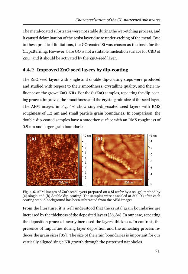
Characterization of the CL-patterned substrates
71
The metal-coated substrates were not stable during the wet-etching process, and
it caused delamination of the resist layer due to under-etching of the metal. Due
to these practical limitations, the GO-coated Si was chosen as the basis for the
CL patterning. However, bare GO is not a suitable nucleation surface for CBD of
ZnO, and it should be activated by the ZnO-seed layer.
4 . 4 . 2 I m prov ed ZnO seed layers by dip-coating
The ZnO seed layers with single and double dip-coating steps were produced
and studied with respect to their smoothness, crystalline quality, and their in-
fluence on the grown ZnO-NRs. For the Si/ZnO samples, repeating the dip-coat-
ing process improved the smoothness and the crystal grain size of the seed layer.
The AFM images in Fig. 4-6 show single-dip-coated seed layers with RMS
roughness of 1.2 nm and small particle grain boundaries. In comparison, the
double-dip-coated samples have a smoother surface with an RMS roughness of
0.9 nm and larger grain boundaries.
Fig. 4-6. AFM images of ZnO seed layers prepared on a Si wafer by a sol-gel method by (a) single and (b) double dip-coating. he samples were annealed at 300 ˚C after each coating step. A background has been subtracted from the AFM images.
From the literature, it is well understood that the crystal grain boundaries are
increased by the thickness of the deposited layers [26, 84]. In our case, repeating
the deposition process linearly increased the layers’ thickness. In contrast, the
presence of impurities during layer deposition and the annealing process re-
duces the grain sizes [85]. The size of the grain boundaries is important for our
vertically aligned single NR growth through the patterned nanoholes.
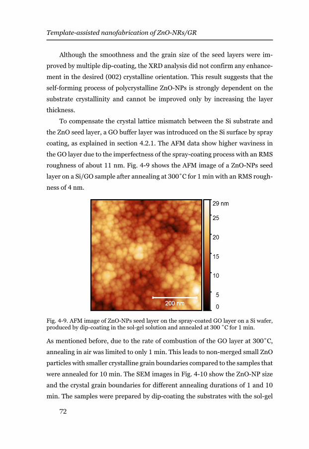
Template-assisted nanofabrication of ZnO-NRs/GR
72
Although the smoothness and the grain size of the seed layers were im-
proved by multiple dip-coating, the XRD analysis did not confirm any enhance-
ment in the desired (002) crystalline orientation. This result suggests that the
self-forming process of polycrystalline ZnO-NPs is strongly dependent on the
substrate crystallinity and cannot be improved only by increasing the layer
thickness.
To compensate the crystal lattice mismatch between the Si substrate and
the ZnO seed layer, a GO buffer layer was introduced on the Si surface by spray
coating, as explained in section 4.2.1. The AFM data show higher waviness in
the GO layer due to the imperfectness of the spray-coating process with an RMS
roughness of about 11 nm. Fig. 4-9 shows the AFM image of a ZnO-NPs seed
la er on a Si/G sample after annealing at 300˚C for 1 min with an S rough-
ness of 4 nm.
Fig. 4-9. AFM image of ZnO-NPs seed layer on the spray-coated GO layer on a Si wafer, produced by dip-coating in the sol-gel solution and annealed at 300 ˚C for 1 min.
As mentioned before, due to the rate of combustion of the G la er at 300˚C,
annealing in air was limited to only 1 min. This leads to non-merged small ZnO
particles with smaller crystalline grain boundaries compared to the samples that
were annealed for 10 min. The SEM images in Fig. 4-10 show the ZnO-NP size
and the crystal grain boundaries for different annealing durations of 1 and 10
min. The samples were prepared by dip-coating the substrates with the sol-gel
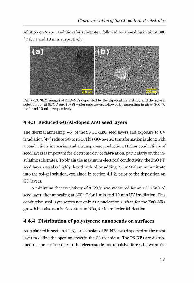
Characterization of the CL-patterned substrates
73
solution on Si/GO and Si-wafer substrates, followed by annealing in air at 300
˚C for 1 and 10 min, respecti el .
Fig. 4-10. SEM images of ZnO-NPs deposited by the dip-coating method and the sol-gel solution on (a) Si/GO and (b) Si-wafer substrates, followed by annealing in air at 300 ˚C for 1 and 10 min, respectively.
4 . 4 . 3 Reduced GO/Al-doped ZnO seed layers
The thermal annealing [46] of the Si/GO/ZnO seed layers and exposure to UV
irradiation [47] reduce GO to rGO. This GO-to-rGO transformation is along with
a conductivity increasing and a transparency reduction. Higher conductivity of
seed layers is important for electronic device fabrication, particularly on the in-
sulating substrates. To obtain the maximum electrical conductivity, the ZnO NP
seed layer was also highly doped with Al by adding 7.5 mM aluminum nitrate
into the sol-gel solution, explained in section 4.1.2, prior to the deposition on
GO layers.
A minimum sheet resisti it of 8 Ω/□ was measured for an rG / n l
seed la er after annealing at 300 ˚C for 1 min and 10 min irradiation. his
conductive seed layer serves not only as a nucleation surface for the ZnO-NRs
growth but also as a back contact to NRs, for later device fabrication.
4 . 4 . 4 Distribution of polystyrene nanobeads on surfaces
As explained in section 4.2.3, a suspension of PS-NBs was dispersed on the resist
layer to define the opening areas in the CL technique. The PS-NBs are distrib-
uted on the surface due to the electrostatic net repulsive forces between the
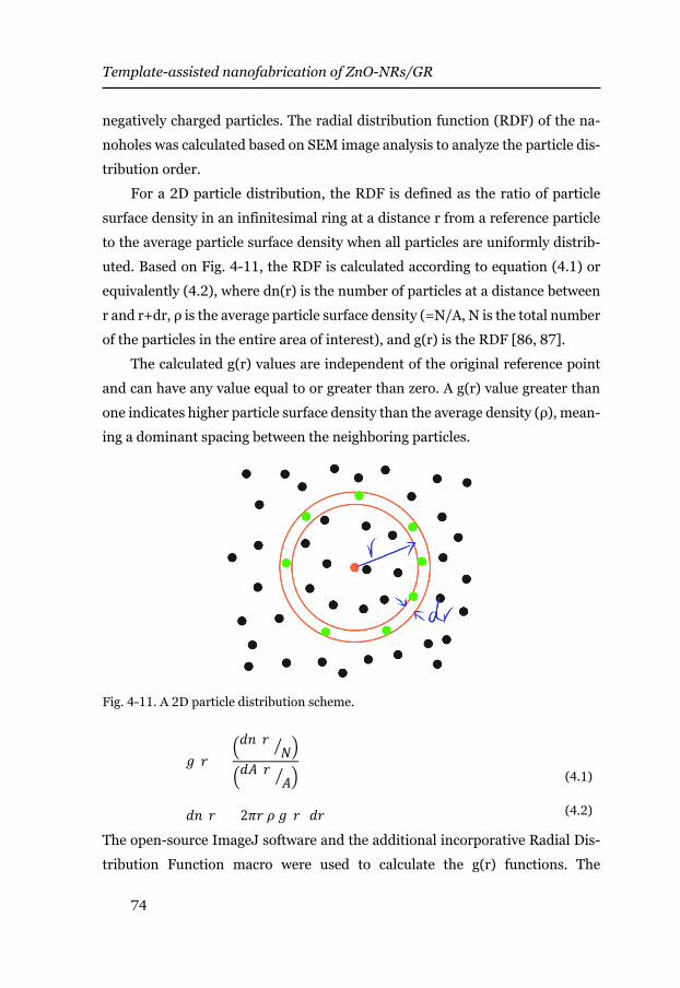
Template-assisted nanofabrication of ZnO-NRs/GR
74
negatively charged particles. The radial distribution function (RDF) of the na-
noholes was calculated based on SEM image analysis to analyze the particle dis-
tribution order.
For a 2D particle distribution, the RDF is defined as the ratio of particle
surface density in an infinitesimal ring at a distance r from a reference particle
to the average particle surface density when all particles are uniformly distrib-
uted. Based on Fig. 4-11, the RDF is calculated according to equation (4.1) or
equivalently (4.2), where dn(r) is the number of particles at a distance between
r and r dr, is the a erage particle surface densit / , is the total number
of the particles in the entire area of interest), and g(r) is the RDF [86, 87].
The calculated g(r) values are independent of the original reference point
and can have any value equal to or greater than zero. A g(r) value greater than
one indicates higher particle surface densit than the a erage densit , mean
ing a dominant spacing between the neighboring particles.
Fig. 4-11. A 2D particle distribution scheme.
𝐷𝐷(𝐷𝐷) =
�𝑑𝑑𝑍𝑍(𝐷𝐷)𝑁𝑁� �
�𝑑𝑑𝐴𝐴(𝐷𝐷)𝐴𝐴� �
(4.1)
𝑑𝑑𝑍𝑍(𝐷𝐷) = 2𝜋𝜋𝐷𝐷 𝜌𝜌 𝐷𝐷(𝐷𝐷) 𝑑𝑑𝐷𝐷 (4.2)
The open-source ImageJ software and the additional incorporative Radial Dis-
tribution Function macro were used to calculate the g(r) functions. The
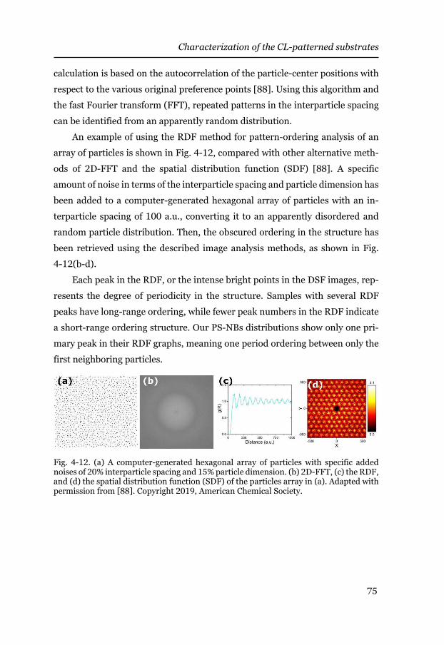
Characterization of the CL-patterned substrates
75
calculation is based on the autocorrelation of the particle-center positions with
respect to the various original preference points [88]. Using this algorithm and
the fast Fourier transform (FFT), repeated patterns in the interparticle spacing
can be identified from an apparently random distribution.
An example of using the RDF method for pattern-ordering analysis of an
array of particles is shown in Fig. 4-12, compared with other alternative meth-
ods of 2D-FFT and the spatial distribution function (SDF) [88]. A specific
amount of noise in terms of the interparticle spacing and particle dimension has
been added to a computer-generated hexagonal array of particles with an in-
terparticle spacing of 100 a.u., converting it to an apparently disordered and
random particle distribution. Then, the obscured ordering in the structure has
been retrieved using the described image analysis methods, as shown in Fig.
4-12(b-d).
Each peak in the RDF, or the intense bright points in the DSF images, rep-
resents the degree of periodicity in the structure. Samples with several RDF
peaks have long-range ordering, while fewer peak numbers in the RDF indicate
a short-range ordering structure. Our PS-NBs distributions show only one pri-
mary peak in their RDF graphs, meaning one period ordering between only the
first neighboring particles.
Fig. 4-12. (a) A computer-generated hexagonal array of particles with specific added noises of 20% interparticle spacing and 15% particle dimension. (b) 2D-FFT, (c) the RDF, and (d) the spatial distribution function (SDF) of the particles array in (a). Adapted with permission from [88]. Copyright 2019, American Chemical Society.

77
5 Conclusions and Outlook
This research work started by exploring potentially 3D-printable conductive
materials with maximum porosity for electronics. Among the possible candi-
dates, ZnO/GR nanocomposites were selected based on their promising electri-
cal and optical properties, and also because of the accumulated knowledge and
experiences for working with ZnO in our research group.
Using a simple and inexpensive solution-based growth technique, several
ZnO-GR nanocomposites with and without doping in various morphologies
were successfully grown and characterized with respect to electrical conductiv-
ity, dispersity, bonding quality between the species, and optical properties. Our
results demonstrate the dependence of the electrical and optical characteristics
of the nanocomposites on the growth parameters, like the pH value.
Optical characterization of the developed composites showed an effective
charge separation at the ZnO-GR interface, which results in a longer lifetime of
the photogenerated charge carriers and enhanced persistent photoconductivity.
In addition, the growth of ZnO-NRs on the GR surface introduced effective spac-
ers, leading to a high porosity in the final structure and significantly promoted
GR wettability, essential for integrating the nanocomposite with other materials
such as polymers for 3D printing.
The observed charge separation mechanism encouraged us to investigate
the photocatalytic performance of our materials. The ZnO-GR nanocomposites
were sensitized to visible light by adding a low bandgap AgI semiconductor to
the composite. A significantly enhanced solar-driven photocatalytic perfor-
mance was observed in the final optimized ZnO/GR/Ag/AgI nanocomposites
due to the increased visible light absorption by AgI, and efficient charge separa-
tion of photogenerated carriers at the ZnO-GR interface.
Conclusions and Outlook
78
To precisely control the growth area, density, and alignment of NRs for ad-
vanced electronics and photonics, a template-assisted selective area growth
method was developed to synthesize arrays of single vertically aligned ZnO-NRs
on Si or glass substrates. This technique is based on colloidal lithography pat-
terning and preparing a compact and uniform ZnO seed layer by a sol-gel and
dip-coating process. Compared to the ZnO-NRs grown on non-patterned sub-
strates, it was shown that much better aligned NRs, with a tunable diameter and
density, can be achieved by our method. However, a (100)-oriented Si substrate
is not the preferred choice of crystalline substrate for vertical ZnO-NR growth.
We developed a novel route to mitigate this problem in Paper IV, where a GO
buffer layer was introduced between the substrate and the ZnO seed layer. A
significant improvement in the ZnO-NR growth was verified using a non-crys-
talline ZnO seed layer on the partially reduced GO (rGO) buffer layer, together
with the previous patterning technique.
A considerable effort was put into realizing a method to produce ordered
arrays of vertical ZnO-NRs. Due to time constraints, the final optimized aligned
structures were not yet tested for exciting applications, e.g., biosensors, LEDs,
or field-emission devices. Due to thermal and oxidation stability, high-aspect
ratio, and controllable length and diameter of the aligned ZnO-NRs on conduc-
tive rGO/ZnO:Al layers, a great potential of these structures is foreseen in all of
the abovementioned applications.
Despite the improvement in vertical alignment of the ZnO-NRs using the
CL-patterning technique, the nanoholes’ exact position is not controllable. To
achieve such a control, precise nanoimprint lithography (NIL) can be employed
to create the desired patterns on the rGO/ZnO seed layers. A more systematic
study is required to optimize the parameters and realize the nanohole patterns
with specific diameter and pitch. Further research, based on this thesis work
deals with developing novel spray-coated conductive and transparent rGO top
contacts for realizing disruptive ZnO NR-based optoelectronics.
79
References
1. Fan W, Zhang Q, Wang Y (2013) Semiconductor-based nanocomposites for photocatalytic H 2 production and CO 2 conversion. Physical Chemis-try Chemical Physics 15:2632–2649. https://doi.org/10.1039/C2CP43524A
2. Wang F, Li Q, Xu D (2017) Recent Progress in Semiconductor-Based Nanocomposite Photocatalysts for Solar-to-Chemical Energy Conversion. Advanced Energy Materials 7:1700529. https://doi.org/10.1002/aenm.201700529
3. Kango S, Kalia S, Celli A, et al (2013) Surface modification of inorganic nanoparticles for development of organic–inorganic nanocomposites—A review. Progress in Polymer Science 38:1232–1261. https://doi.org/10.1016/j.progpolymsci.2013.02.003
4. Gao N, Fang X (2015) Synthesis and Development of Graphene–Inorganic Semiconductor Nanocomposites. Chem Rev 115:8294–8343. https://doi.org/10.1021/cr400607y
5. Kim Y-J, Lee J-H, Yi G-C (2009) Vertically aligned ZnO nanostructures grown on graphene layers. Applied Physics Letters 95:213101. https://doi.org/10.1063/1.3266836
6. Lee JM, Pyun YB, Yi J, et al (2009) ZnO Nanorod−Graphene Hybrid Ar-chitectures for Multifunctional Conductors. J Phys Chem C 113:19134–19138. https://doi.org/10.1021/jp9078713
7. Lin J, Penchev M, Wang G, et al (2010) Heterogeneous Graphene Nanostructures: ZnO Nanostructures Grown on Large-Area Graphene Layers. Small 6:2448–2452. https://doi.org/10.1002/smll.201000250
8. Kim Y-J, Hadiyawarman, Yoon A, et al (2011) Hydrothermally grown ZnO nanostructures on few-layer graphene sheets. Nanotechnology 22:245603. https://doi.org/10.1088/0957-4484/22/24/245603
9. Chandraiahgari CR, Bellis GD, Balijepalli SK, et al (2016) Control of the size and density of ZnO-nanorods grown onto graphene nanoplatelets in
80
aqueous suspensions. RSC Adv 6:83217–83225. https://doi.org/10.1039/C6RA18317D
10. Munshi AM, Dheeraj DL, Fauske VT, et al (2012) Vertically Aligned GaAs Nanowires on Graphite and Few-Layer Graphene: Generic Model and Ep-itaxial Growth. Nano Lett 12:4570–4576. https://doi.org/10.1021/nl3018115
11. Hwang JO, Lee DH, Kim JY, et al (2011) Vertical ZnO nanowires/gra-phene hybrids for transparent and flexible field emission. J Mater Chem 21:3432–3437. https://doi.org/10.1039/C0JM01495H
12. Di Bartolomeo A (2016) Graphene Schottky diodes: An experimental re-view of the rectifying graphene/semiconductor heterojunction. Physics Reports 606:1–58. https://doi.org/10.1016/j.physrep.2015.10.003
13. Ertekin E, Greaney PA, Sands TD, Chrzan DC (2002) Equilibrium Analysis of Lattice-Mismatched Nanowire Heterostructures. MRS Online Proceed-ings Library Archive 737:. https://doi.org/10.1557/PROC-737-F10.4
14. Sandiumenge F (2017) Strain landscapes and self-organization of free sur-faces in complex oxide epitaxy. Journal of Materials Research 32:3958–3976. https://doi.org/10.1557/jmr.2017.317
15. Kołodziejczak-Radzimska A, Jesionowski T (2014) Zinc Oxide—From Synthesis to Application: A Review. Materials 7:2833–2881. https://doi.org/10.3390/ma7042833
16. Klingshirn C, Fallert J, Zhou H, et al (2010) 65 years of ZnO research – old and very recent results. phys stat sol (b) 247:1424–1447. https://doi.org/10.1002/pssb.200983195
17. Janotti A, Van de Walle CG (2006) New insights into the role of native point defects in ZnO. Journal of Crystal Growth 287:58–65. https://doi.org/10.1016/j.jcrysgro.2005.10.043
18. Janotti A, Van de Walle CG (2007) Native point defects in ZnO. Phys Rev B 76:165202. https://doi.org/10.1103/PhysRevB.76.165202
19. Janotti A, Walle CGV de (2009) Fundamentals of zinc oxide as a semicon-ductor. Rep Prog Phys 72:126501. https://doi.org/10.1088/0034-4885/72/12/126501
20. Choi S, Phillips MR, Aharonovich I, et al (2015) Photophysics of Point De-fects in ZnO Nanoparticles. Advanced Optical Materials 3:821–827. https://doi.org/10.1002/adom.201400592
81
21. Galdámez-Martinez A, Santana G, Güell F, et al (2020) Photolumines-cence of ZnO Nanowires: A Review. Nanomaterials 10:857. https://doi.org/10.3390/nano10050857
22. Liu R, Chen Y, Ding S, et al (2019) Preparation of highly transparent con-ductive aluminum-doped zinc oxide thin films using a low-temperature aqueous solution process for thin-film solar cells applications. Solar En-ergy Materials and Solar Cells 203:110161. https://doi.org/10.1016/j.solmat.2019.110161
23. Hsu C-H, Chen D-H (2010) Synthesis and conductivity enhancement of Al-doped ZnO nanorod array thin films. Nanotechnology 21:285603. https://doi.org/10.1088/0957-4484/21/28/285603
24. Hagendorfer H, Lienau K, Nishiwaki S, et al (2014) Highly Transparent and Conductive ZnO: Al Thin Films from a Low Temperature Aqueous So-lution Approach. Adv Mater 26:632–636. https://doi.org/10.1002/adma.201303186
25. Bamiduro O, Mustafa H, Mundle R, et al (2007) Metal-like conductivity in transparent Al:ZnO films. Appl Phys Lett 90:252108. https://doi.org/10.1063/1.2749836
26. Nian Q, Callahan M, Look D, et al (2015) Highly transparent conductive electrode with ultra-low HAZE by grain boundary modification of aqueous solution fabricated alumina-doped zinc oxide nanocrystals. APL Materials 3:062803. https://doi.org/10.1063/1.4915489
27. Jia J, Takasaki A, Oka N, Shigesato Y (2012) Experimental observation on the Fermi level shift in polycrystalline Al-doped ZnO films. Journal of Ap-plied Physics 112:013718. https://doi.org/10.1063/1.4733969
28. Consonni V, Lord AM (2021) Polarity in ZnO nanowires: A critical issue for piezotronic and piezoelectric devices. Nano Energy 83:105789. https://doi.org/10.1016/j.nanoen.2021.105789
29. Song Y, Wang N, Fadlallah MM, et al (2021) Defect states contributed na-noscale contact electrification at ZnO nanowires packed film surfaces. Nano Energy 79:105406. https://doi.org/10.1016/j.nanoen.2020.105406
30. Azulay AR, Turkulets Y, Gaudio DD, et al (2020) Why do nanowires grow with their c-axis vertically-aligned in the absence of epitaxy? Scientific Re-ports 10:6554. https://doi.org/10.1038/s41598-020-63500-y
31. Cossuet T, Roussel H, Chauveau J-M, et al (2018) Well-ordered ZnO nan-owires with controllable inclination on semipolar ZnO surfaces by
82
chemical bath deposition. Nanotechnology 29:475601. https://doi.org/10.1088/1361-6528/aadf62
32. Mitra P, Chatterjee AP, Maiti HS (1998) ZnO thin film sensor. Materials Letters 35:33–38. https://doi.org/10.1016/S0167-577X(97)00215-2
33. Zhu Q, Xie C, Li H, Zeng D (2016) A method for modeling and deciphering the persistent photoconductance and long-term charge storage of ZnO na-norod arrays. Nano Res 9:2972–3002. https://doi.org/10.1007/s12274-016-1182-y
34. Wu XL, Siu GG, Fu CL, Ong HC (2001) Photoluminescence and cathodo-luminescence studies of stoichiometric and oxygen-deficient ZnO films. Appl Phys Lett 78:2285–2287. https://doi.org/10.1063/1.1361288
35. Zhu Q, Xie C, Li H, et al (2015) Through-Process Analytical Modeling of Photoconductance Spectrum for Porous ZnO Nanocrystalline Film. Chem Mater 27:2861–2874. https://doi.org/10.1021/cm504739f
36. Moore JC, Thompson CV (2013) A Phenomenological Model for the Pho-tocurrent Transient Relaxation Observed in ZnO-Based Photodetector De-vices. Sensors (Basel) 13:9921–9940. https://doi.org/10.3390/s130809921
37. Edinger S, Bansal N, Bauch M, et al (2017) Comparison of chemical bath-deposited ZnO films doped with Al, Ga and In. J Mater Sci 52:9410–9423. https://doi.org/10.1007/s10853-017-1104-8
38. Weiss NO, Zhou H, Liao L, et al (2012) Graphene: An Emerging Electronic Material. Adv Mater 24:5782–5825. https://doi.org/10.1002/adma.201201482
39. (2017) Nanotechnologies-Vocabulary-Part 13: Graphene and Related Two-Dimensional (2D) Materials
40. Pollard AJ, Paton KR, Clifford CA, Legge E (2017) Characterisation of the structure of graphene
41. Gee C-M, Tseng C-C, Wu F-Y, et al (2013) Flexible transparent electrodes made of electrochemically exfoliated graphene sheets from low-cost graphite pieces. Displays 34:315–319. https://doi.org/10.1016/j.dis-pla.2012.11.002
42. Arapov K, Rubingh E, Abbel R, et al (2016) Conductive Screen Printing Inks by Gelation of Graphene Dispersions. Adv Funct Mater 26:586–593. https://doi.org/10.1002/adfm.201504030
83
43. Yu H, Zhang B, Bulin C, et al (2016) High-efficient Synthesis of Graphene Oxide Based on Improved Hummers Method. Scientific Reports 6:36143. https://doi.org/10.1038/srep36143
44. Chen J, Yao B, Li C, Shi G (2013) An improved Hummers method for eco-friendly synthesis of graphene oxide. Carbon 64:225–229. https://doi.org/10.1016/j.carbon.2013.07.055
45. Marcano DC, Kosynkin DV, Berlin JM, et al (2010) Improved Synthesis of Graphene Oxide. ACS Nano 4:4806–4814. https://doi.org/10.1021/nn1006368
46. Sengupta I, Chakraborty S, Talukdar M, et al (2018) Thermal reduction of graphene oxide: How temperature influences purity. Journal of Materials Research 33:4113–4122. https://doi.org/10.1557/jmr.2018.338
47. Ji T, Hua Y, Sun M, Ma N (2013) The mechanism of the reaction of graph-ite oxide to reduced graphene oxide under ultraviolet irradiation. Carbon 54:412–418. https://doi.org/10.1016/j.carbon.2012.11.057
48. Jariwala D, Marks TJ, Hersam MC (2017) Mixed-dimensional van der Waals heterostructures. Nature Materials 16:170–181. https://doi.org/10.1038/nmat4703
49. Choi WM, Shin K-S, Lee HS, et al (2011) Selective growth of ZnO nanorods on SiO2/Si substrates using a graphene buffer layer. Nano Res 4:440–447. https://doi.org/10.1007/s12274-011-0100-6
50. Larson K, Clark A, Appel A, et al (2015) Surface-dependence of interfacial binding strength between zinc oxide and graphene. RSC Advances 5:65719–65724. https://doi.org/10.1039/C5RA13048D
51. Müller R, Huber F, Gelme O, et al (2019) Chemical Vapor Deposition Growth of Zinc Oxide on Sapphire with Methane: Initial Crystal For-mation Process. Crystal Growth & Design 19:4964–4969. https://doi.org/10.1021/acs.cgd.9b00181
52. Gomez JL, Tigli O (2013) Zinc oxide nanostructures: from growth to ap-plication. J Mater Sci 48:612–624. https://doi.org/10.1007/s10853-012-6938-5
53. Rahman F (2019) Zinc oxide light-emitting diodes: a review. OE 58:010901. https://doi.org/10.1117/1.OE.58.1.010901
54. Gardeniers JGE, Rittersma ZM, Burger GJ (1998) Preferred orientation and piezoelectricity in sputtered ZnO films. Journal of Applied Physics 83:7844–7854. https://doi.org/10.1063/1.367959
84
55. Bacaksiz E, Parlak M, Tomakin M, et al (2008) The effects of zinc nitrate, zinc acetate and zinc chloride precursors on investigation of structural and optical properties of ZnO thin films. Journal of Alloys and Compounds 466:447–450. https://doi.org/10.1016/j.jallcom.2007.11.061
56. Yun S, Lee J, Yang J, Lim S (2010) Hydrothermal synthesis of Al-doped ZnO nanorod arrays on Si substrate. Physica B: Condensed Matter 405:413–419. https://doi.org/10.1016/j.physb.2009.08.297
57. Gao Y, Nagai M (2006) Morphology Evolution of ZnO Thin Films from Aqueous Solutions and Their Application to Solar Cells. Langmuir 22:3936–3940. https://doi.org/10.1021/la053042f
58. Vayssieres L (2003) Growth of Arrayed Nanorods and Nanowires of ZnO from Aqueous Solutions. Adv Mater 15:464–466. https://doi.org/10.1002/adma.200390108
59. Sakai D, Nagashima K, Yoshida H, et al (2019) Substantial Narrowing on the Width of “Concentration Window” of Hydrothermal ZnO Nanowires via Ammonia Addition. Sci Rep 9:1–10. https://doi.org/10.1038/s41598-019-50641-y
60. Chalangar E, Machhadani H, Lim S-H, et al (2018) Influence of morphol-ogy on electrical and optical properties of graphene/Al-doped ZnO-nano-rod composites. Nanotechnology 29:415201. https://doi.org/10.1088/1361-6528/aad3ec
61. Fuchs P, Hagendorfer H, Romanyuk YE, Tiwari AN (2015) Doping strate-gies for highly conductive Al-doped ZnO films grown from aqueous solu-tion. Phys Status Solidi A 212:51–55. https://doi.org/10.1002/pssa.201431145
62. Verrier C, Appert E, Chaix-Pluchery O, et al (2017) Effects of the pH on the Formation and Doping Mechanisms of ZnO Nanowires Using Alumi-num Nitrate and Ammonia. Inorg Chem 56:13111–13122. https://doi.org/10.1021/acs.inorgchem.7b01916
63. Gfroerer TH (2006) Photoluminescence in Analysis of Surfaces and Inter-faces. In: Encyclopedia of Analytical Chemistry. John Wiley & Sons, Ltd
64. Smits FM (1958) Measurement of Sheet Resistivities with the Four-Point Probe. Bell System Technical Journal 37:711–718. https://doi.org/10.1002/j.1538-7305.1958.tb03883.x
65. Rani M, Tripathi SK (2016) Electron transfer properties of organic dye sensitized ZnO and ZnO/TiO2 photoanode for dye sensitized solar cells.
85
Renewable and Sustainable Energy Reviews 61:97–107. https://doi.org/10.1016/j.rser.2016.03.012
66. Xu S, Wang ZL (2011) One-dimensional ZnO nanostructures: Solution growth and functional properties. Nano Res 4:1013–1098. https://doi.org/10.1007/s12274-011-0160-7
67. Li Y, Li X, Li J, Yin J (2006) Photocatalytic degradation of methyl orange by TiO2-coated activated carbon and kinetic study. Water Research 40:1119–1126. https://doi.org/10.1016/j.watres.2005.12.042
68. Zhu Q, Xie C, Li H, et al (2014) Selectively enhanced UV and NIR photo-luminescence from a degenerate ZnO nanorod array film. Journal of Ma-terials Chemistry C 2:4566–4580. https://doi.org/10.1039/C4TC00011K
69. Rahman MM, Khan MKR, Islam MR, et al (2012) Effect of Al Doping on Structural, Electrical, Optical and Photoluminescence Properties of Nano-Structural ZnO Thin Films. Journal of Materials Science & Technology 28:329–335. https://doi.org/10.1016/S1005-0302(12)60064-4
70. Chalangar E (2019) Graphene-based nanocomposites for electronics and photocatalysis. Linköping University Electronic Press, Linköping
71. Li G, Wang Y, Mao L (2014) Recent progress in highly efficient Ag-based visible-light photocatalysts. RSC Adv 4:53649–53661. https://doi.org/10.1039/C4RA08044K
72. Kaspar TC, Droubay T, Chambers SA, Bagus PS (2010) Spectroscopic Ev-idence for Ag(III) in Highly Oxidized Silver Films by X-ray Photoelectron Spectroscopy. J Phys Chem C 114:21562–21571. https://doi.org/10.1021/jp107914e
73. Adam RE, Chalangar E, Pirhashemi M, et al (2019) Graphene-based plas-monic nanocomposites for highly enhanced solar-driven photocatalytic activities. RSC Adv 9:30585–30598. https://doi.org/10.1039/C9RA06273D
74. Wissler M (2006) Graphite and carbon powders for electrochemical appli-cations. Journal of Power Sources 156:142–150. https://doi.org/10.1016/j.jpowsour.2006.02.064
75. Parize R, Garnier JD, Appert E, et al (2018) Effects of Polyethylenimine and Its Molecular Weight on the Chemical Bath Deposition of ZnO Nan-owires. ACS Omega 3:12457–12464. https://doi.org/10.1021/acsomega.8b01641
86
76. Verrier C, Appert E, Chaix-Pluchery O, et al (2017) Tunable Morphology and Doping of ZnO Nanowires by Chemical Bath Deposition Using Alumi-num Nitrate. J Phys Chem C 121:3573–3583. https://doi.org/10.1021/acs.jpcc.6b11104
77. Xu S, Wei Y, Kirkham M, et al (2008) Patterned Growth of Vertically Aligned ZnO Nanowire Arrays on Inorganic Substrates at Low Tempera-ture without Catalyst. J Am Chem Soc 130:14958–14959. https://doi.org/10.1021/ja806952j
78. Fredriksson H, Alaverdyan Y, Dmitriev A, et al (2007) Hole–Mask Colloi-dal Lithography. Advanced Materials 19:4297–4302. https://doi.org/10.1002/adma.200700680
79. Hanarp P, Sutherland D, Gold J, Kasemo B (1999) Nanostructured model biomaterial surfaces prepared by colloidal lithography. Nanostructured Materials 12:429–432. https://doi.org/10.1016/S0965-9773(99)00151-8
80. Cesaria M, Taurino A, Manera MG, et al (2019) Gold nanoholes fabricated by colloidal lithography: novel insights into nanofabrication, short-range correlation and optical properties. Nanoscale 11:8416–8432. https://doi.org/10.1039/C8NR09911A
81. Chalangar E, Nur O, Willander M, et al (2021) Synthesis of Vertically Aligned ZnO Nanorods Using Sol-gel Seeding and Colloidal Lithography Patterning. Nanoscale Research Letters 16:46. https://doi.org/10.1186/s11671-021-03500-7
82. Vellekoop MJ, Visser CCO, Sarro PM, Venema A (1990) Compatibility of zinc oxide with silicon IC processing. Sensors and Actuators A: Physical 23:1027–1030. https://doi.org/10.1016/0924-4247(90)87083-U
83. Meyer E, Hug HJ, Bennewitz R (2004) Scanning Probe Microscopy: The Lab on a Tip. Springer-Verlag, Berlin Heidelberg
84. Kumar M, Kanjilal A, Som T (2013) Effect of grain-boundaries on electri-cal properties of n-ZnO:Al/p-Si heterojunction diodes. AIP Advances 3:092126. https://doi.org/10.1063/1.4823480
85. Bandyopadhyay S, Paul GK, Roy R, et al (2002) Study of structural and electrical properties of grain-boundary modified ZnO films prepared by sol–gel technique. Materials Chemistry and Physics 74:83–91. https://doi.org/10.1016/S0254-0584(01)00402-3
86. Younge K, Johnston B, Christenson C, et al (2006) The use of radial distri-bution and pair-correlation functions to analyze and describe biological

87
aggregations. Limnology and Oceanography: Methods 4:382–391. https://doi.org/10.4319/lom.2006.4.382
87. Thorneywork AL, Roth R, Aarts DGAL, Dullens RPA (2014) Communica-tion: Radial distribution functions in a two-dimensional binary colloidal hard sphere system. J Chem Phys 140:161106. https://doi.org/10.1063/1.4872365
88. Mac Fhionnlaoich N, Qi R, Guldin S (2019) Application of the Spatial Dis-tribution Function to Colloidal Ordering. Langmuir 35:16605–16611. https://doi.org/10.1021/acs.langmuir.9b02877


89
Part II: Papers

90

PAPER I
91

92
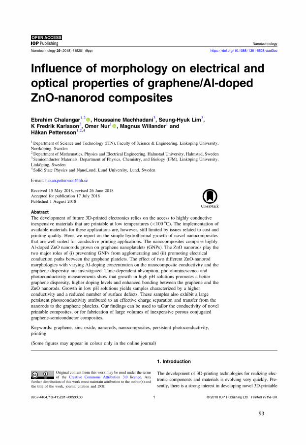
Influence of morphology on electrical andoptical properties of graphene/Al-dopedZnO-nanorod composites
Ebrahim Chalangar1,2 , Houssaine Machhadani3, Seung-Hyuk Lim3,K Fredrik Karlsson3, Omer Nur1 , Magnus Willander1 andHåkan Pettersson1,2,4
1Department of Science and Technology (ITN), Faculty of Science & Engineering, Linköping University,Norrköping, Sweden2Department of Mathematics, Physics and Electrical Engineering, Halmstad University, Halmstad, Sweden3 Semiconductor Materials, Department of Physics, Chemistry, and Biology (IFM), Linköping University,Linköping, Sweden4 Solid State Physics and NanoLund, Lund University, Lund, Sweden
E-mail: [email protected]
Received 15 May 2018, revised 26 June 2018Accepted for publication 17 July 2018Published 1 August 2018
AbstractThe development of future 3D-printed electronics relies on the access to highly conductiveinexpensive materials that are printable at low temperatures (<100 ◦C). The implementation ofavailable materials for these applications are, however, still limited by issues related to cost andprinting quality. Here, we report on the simple hydrothermal growth of novel nanocompositesthat are well suited for conductive printing applications. The nanocomposites comprise highlyAl-doped ZnO nanorods grown on graphene nanoplatelets (GNPs). The ZnO nanorods play thetwo major roles of (i) preventing GNPs from agglomerating and (ii) promoting electricalconduction paths between the graphene platelets. The effect of two different ZnO-nanorodmorphologies with varying Al-doping concentration on the nanocomposite conductivity and thegraphene dispersity are investigated. Time-dependent absorption, photoluminescence andphotoconductivity measurements show that growth in high pH solutions promotes a bettergraphene dispersity, higher doping levels and enhanced bonding between the graphene and theZnO nanorods. Growth in low pH solutions yields samples characterized by a higherconductivity and a reduced number of surface defects. These samples also exhibit a largepersistent photoconductivity attributed to an effective charge separation and transfer from thenanorods to the graphene platelets. Our findings can be used to tailor the conductivity of novelprintable composites, or for fabrication of large volumes of inexpensive porous conjugatedgraphene-semiconductor composites.
Keywords: graphene, zinc oxide, nanorods, nanocomposites, persistent photoconductivity,printing
(Some figures may appear in colour only in the online journal)
1. Introduction
The development of 3D-printing technologies for realizing elec-tronic components and materials is evolving very quickly. Pre-sently, there is a strong interest in developing novel 3D-printable
Nanotechnology
Nanotechnology 29 (2018) 415201 (8pp) https://doi.org/10.1088/1361-6528/aad3ec
Original content from this work may be used under the termsof the Creative Commons Attribution 3.0 licence. Any
further distribution of this work must maintain attribution to the author(s) andthe title of the work, journal citation and DOI.
0957-4484/18/415201+08$33.00 © 2018 IOP Publishing Ltd Printed in the UK1
93
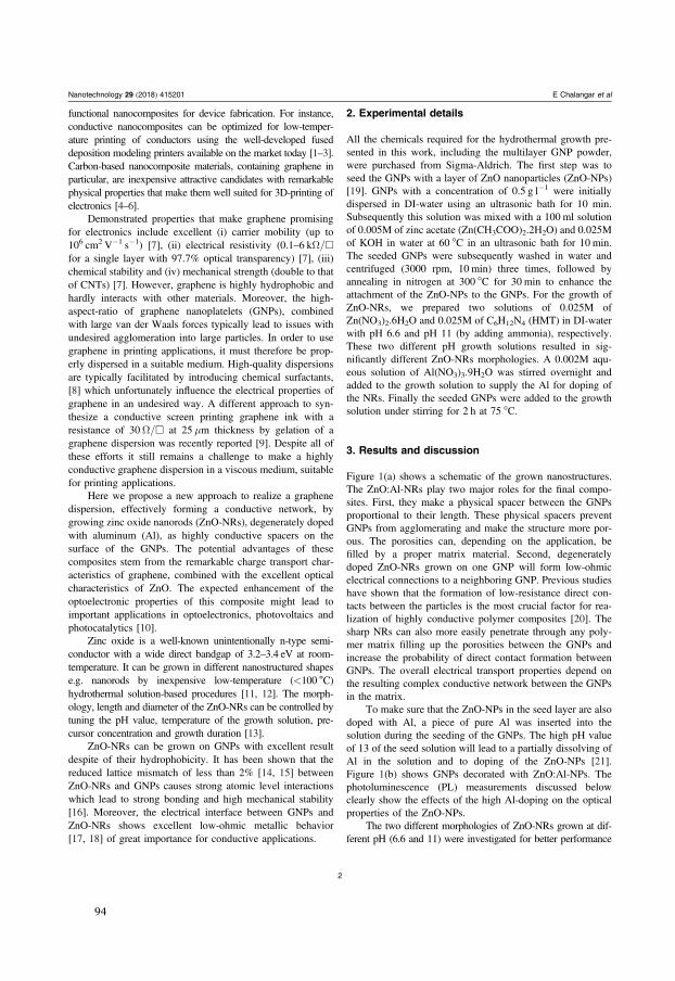
functional nanocomposites for device fabrication. For instance,conductive nanocomposites can be optimized for low-temper-ature printing of conductors using the well-developed fuseddeposition modeling printers available on the market today [1–3].Carbon-based nanocomposite materials, containing graphene inparticular, are inexpensive attractive candidates with remarkablephysical properties that make them well suited for 3D-printing ofelectronics [4–6].
Demonstrated properties that make graphene promisingfor electronics include excellent (i) carrier mobility (up to106 cm2 V−1 s−1) [7], (ii) electrical resistivity (0.1–6 kΩ/,for a single layer with 97.7% optical transparency) [7], (iii)chemical stability and (iv) mechanical strength (double to thatof CNTs) [7]. However, graphene is highly hydrophobic andhardly interacts with other materials. Moreover, the high-aspect-ratio of graphene nanoplatelets (GNPs), combinedwith large van der Waals forces typically lead to issues withundesired agglomeration into large particles. In order to usegraphene in printing applications, it must therefore be prop-erly dispersed in a suitable medium. High-quality dispersionsare typically facilitated by introducing chemical surfactants,[8] which unfortunately influence the electrical properties ofgraphene in an undesired way. A different approach to syn-thesize a conductive screen printing graphene ink with aresistance of 30Ω/, at 25 μm thickness by gelation of agraphene dispersion was recently reported [9]. Despite all ofthese efforts it still remains a challenge to make a highlyconductive graphene dispersion in a viscous medium, suitablefor printing applications.
Here we propose a new approach to realize a graphenedispersion, effectively forming a conductive network, bygrowing zinc oxide nanorods (ZnO-NRs), degenerately dopedwith aluminum (Al), as highly conductive spacers on thesurface of the GNPs. The potential advantages of thesecomposites stem from the remarkable charge transport char-acteristics of graphene, combined with the excellent opticalcharacteristics of ZnO. The expected enhancement of theoptoelectronic properties of this composite might lead toimportant applications in optoelectronics, photovoltaics andphotocatalytics [10].
Zinc oxide is a well-known unintentionally n-type semi-conductor with a wide direct bandgap of 3.2–3.4 eV at room-temperature. It can be grown in different nanostructured shapese.g. nanorods by inexpensive low-temperature (<100 ◦C)hydrothermal solution-based procedures [11, 12]. The morph-ology, length and diameter of the ZnO-NRs can be controlled bytuning the pH value, temperature of the growth solution, pre-cursor concentration and growth duration [13].
ZnO-NRs can be grown on GNPs with excellent resultdespite of their hydrophobicity. It has been shown that thereduced lattice mismatch of less than 2% [14, 15] betweenZnO-NRs and GNPs causes strong atomic level interactionswhich lead to strong bonding and high mechanical stability[16]. Moreover, the electrical interface between GNPs andZnO-NRs shows excellent low-ohmic metallic behavior[17, 18] of great importance for conductive applications.
2. Experimental details
All the chemicals required for the hydrothermal growth pre-sented in this work, including the multilayer GNP powder,were purchased from Sigma-Aldrich. The first step was toseed the GNPs with a layer of ZnO nanoparticles (ZnO-NPs)[19]. GNPs with a concentration of 0.5 g l−1 were initiallydispersed in DI-water using an ultrasonic bath for 10 min.Subsequently this solution was mixed with a 100 ml solutionof 0.005M of zinc acetate (Zn(CH3COO)2.2H2O) and 0.025Mof KOH in water at 60 °C in an ultrasonic bath for 10 min.The seeded GNPs were subsequently washed in water andcentrifuged (3000 rpm, 10 min) three times, followed byannealing in nitrogen at 300 °C for 30 min to enhance theattachment of the ZnO-NPs to the GNPs. For the growth ofZnO-NRs, we prepared two solutions of 0.025M ofZn(NO3)2.6H2O and 0.025M of C6H12N4 (HMT) in DI-waterwith pH 6.6 and pH 11 (by adding ammonia), respectively.These two different pH growth solutions resulted in sig-nificantly different ZnO-NRs morphologies. A 0.002M aqu-eous solution of Al(NO3)3.9H2O was stirred overnight andadded to the growth solution to supply the Al for doping ofthe NRs. Finally the seeded GNPs were added to the growthsolution under stirring for 2 h at 75 °C.
3. Results and discussion
Figure 1(a) shows a schematic of the grown nanostructures.The ZnO:Al-NRs play two major roles for the final compo-sites. First, they make a physical spacer between the GNPsproportional to their length. These physical spacers preventGNPs from agglomerating and make the structure more por-ous. The porosities can, depending on the application, befilled by a proper matrix material. Second, degeneratelydoped ZnO-NRs grown on one GNP will form low-ohmicelectrical connections to a neighboring GNP. Previous studieshave shown that the formation of low-resistance direct con-tacts between the particles is the most crucial factor for rea-lization of highly conductive polymer composites [20]. Thesharp NRs can also more easily penetrate through any poly-mer matrix filling up the porosities between the GNPs andincrease the probability of direct contact formation betweenGNPs. The overall electrical transport properties depend onthe resulting complex conductive network between the GNPsin the matrix.
To make sure that the ZnO-NPs in the seed layer are alsodoped with Al, a piece of pure Al was inserted into thesolution during the seeding of the GNPs. The high pH valueof 13 of the seed solution will lead to a partially dissolving ofAl in the solution and to doping of the ZnO-NPs [21].Figure 1(b) shows GNPs decorated with ZnO:Al-NPs. Thephotoluminescence (PL) measurements discussed belowclearly show the effects of the high Al-doping on the opticalproperties of the ZnO-NPs.
The two different morphologies of ZnO-NRs grown at dif-ferent pH (6.6 and 11) were investigated for better performance
2
Nanotechnology 29 (2018) 415201 E Chalangar et al
94
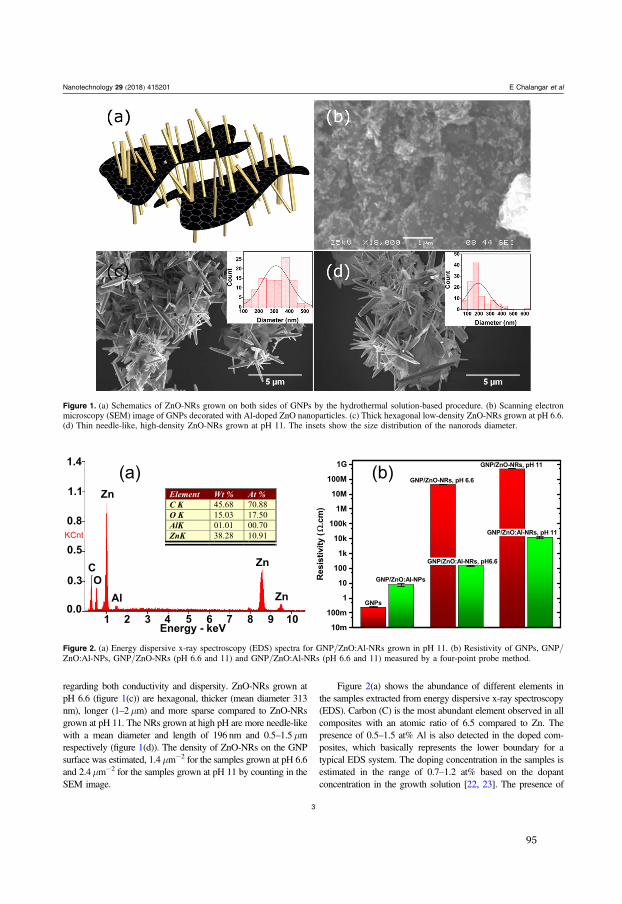
regarding both conductivity and dispersity. ZnO-NRs grown atpH 6.6 (figure 1(c)) are hexagonal, thicker (mean diameter 313nm), longer (1–2μm) and more sparse compared to ZnO-NRsgrown at pH 11. The NRs grown at high pH are more needle-likewith a mean diameter and length of 196 nm and 0.5–1.5μmrespectively (figure 1(d)). The density of ZnO-NRs on the GNPsurface was estimated, 1.4μm−2 for the samples grown at pH 6.6and 2.4μm−2 for the samples grown at pH 11 by counting in theSEM image.
Figure 2(a) shows the abundance of different elements inthe samples extracted from energy dispersive x-ray spectroscopy(EDS). Carbon (C) is the most abundant element observed in allcomposites with an atomic ratio of 6.5 compared to Zn. Thepresence of 0.5–1.5 at% Al is also detected in the doped com-posites, which basically represents the lower boundary for atypical EDS system. The doping concentration in the samples isestimated in the range of 0.7–1.2 at% based on the dopantconcentration in the growth solution [22, 23]. The presence of
Figure 1. (a) Schematics of ZnO-NRs grown on both sides of GNPs by the hydrothermal solution-based procedure. (b) Scanning electronmicroscopy (SEM) image of GNPs decorated with Al-doped ZnO nanoparticles. (c) Thick hexagonal low-density ZnO-NRs grown at pH 6.6.(d) Thin needle-like, high-density ZnO-NRs grown at pH 11. The insets show the size distribution of the nanorods diameter.
Figure 2. (a) Energy dispersive x-ray spectroscopy (EDS) spectra for GNP/ZnO:Al-NRs grown in pH 11. (b) Resistivity of GNPs, GNP/ZnO:Al-NPs, GNP/ZnO-NRs (pH 6.6 and 11) and GNP/ZnO:Al-NRs (pH 6.6 and 11) measured by a four-point probe method.
3
Nanotechnology 29 (2018) 415201 E Chalangar et al
95
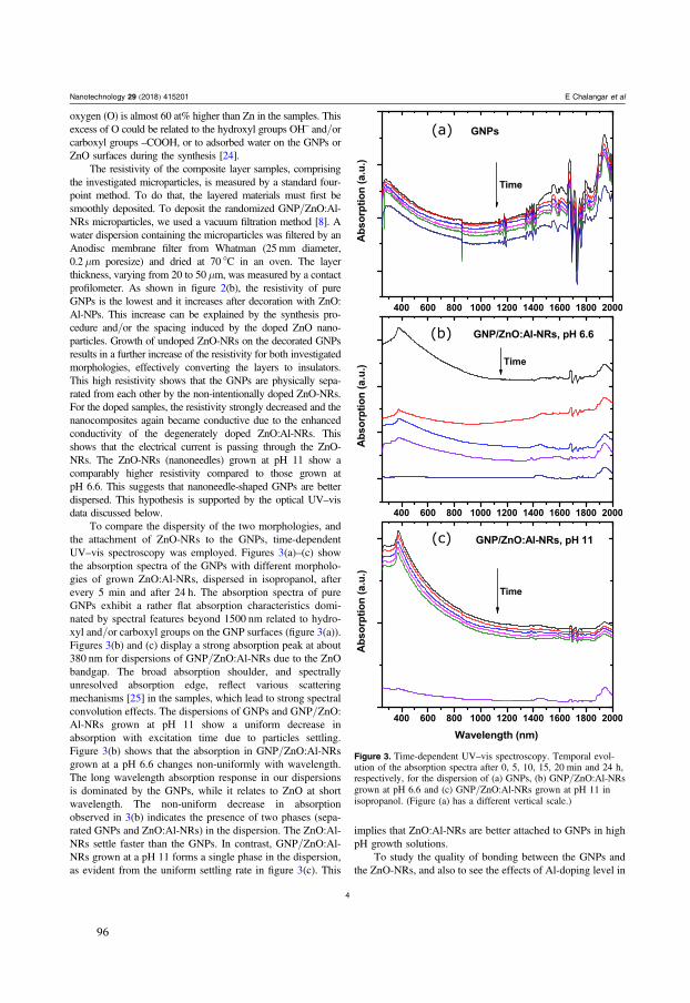
oxygen (O) is almost 60 at% higher than Zn in the samples. Thisexcess of O could be related to the hydroxyl groups OH– and/orcarboxyl groups –COOH, or to adsorbed water on the GNPs orZnO surfaces during the synthesis [24].
The resistivity of the composite layer samples, comprisingthe investigated microparticles, is measured by a standard four-point method. To do that, the layered materials must first besmoothly deposited. To deposit the randomized GNP/ZnO:Al-NRs microparticles, we used a vacuum filtration method [8]. Awater dispersion containing the microparticles was filtered by anAnodisc membrane filter from Whatman (25mm diameter,0.2 μm poresize) and dried at 70 °C in an oven. The layerthickness, varying from 20 to 50 μm, was measured by a contactprofilometer. As shown in figure 2(b), the resistivity of pureGNPs is the lowest and it increases after decoration with ZnO:Al-NPs. This increase can be explained by the synthesis pro-cedure and/or the spacing induced by the doped ZnO nano-particles. Growth of undoped ZnO-NRs on the decorated GNPsresults in a further increase of the resistivity for both investigatedmorphologies, effectively converting the layers to insulators.This high resistivity shows that the GNPs are physically sepa-rated from each other by the non-intentionally doped ZnO-NRs.For the doped samples, the resistivity strongly decreased and thenanocomposites again became conductive due to the enhancedconductivity of the degenerately doped ZnO:Al-NRs. Thisshows that the electrical current is passing through the ZnO-NRs. The ZnO-NRs (nanoneedles) grown at pH 11 show acomparably higher resistivity compared to those grown atpH 6.6. This suggests that nanoneedle-shaped GNPs are betterdispersed. This hypothesis is supported by the optical UV–visdata discussed below.
To compare the dispersity of the two morphologies, andthe attachment of ZnO-NRs to the GNPs, time-dependentUV–vis spectroscopy was employed. Figures 3(a)–(c) showthe absorption spectra of the GNPs with different morpholo-gies of grown ZnO:Al-NRs, dispersed in isopropanol, afterevery 5 min and after 24 h. The absorption spectra of pureGNPs exhibit a rather flat absorption characteristics domi-nated by spectral features beyond 1500 nm related to hydro-xyl and/or carboxyl groups on the GNP surfaces (figure 3(a)).Figures 3(b) and (c) display a strong absorption peak at about380 nm for dispersions of GNP/ZnO:Al-NRs due to the ZnObandgap. The broad absorption shoulder, and spectrallyunresolved absorption edge, reflect various scatteringmechanisms [25] in the samples, which lead to strong spectralconvolution effects. The dispersions of GNPs and GNP/ZnO:Al-NRs grown at pH 11 show a uniform decrease inabsorption with excitation time due to particles settling.Figure 3(b) shows that the absorption in GNP/ZnO:Al-NRsgrown at a pH 6.6 changes non-uniformly with wavelength.The long wavelength absorption response in our dispersionsis dominated by the GNPs, while it relates to ZnO at shortwavelength. The non-uniform decrease in absorptionobserved in 3(b) indicates the presence of two phases (sepa-rated GNPs and ZnO:Al-NRs) in the dispersion. The ZnO:Al-NRs settle faster than the GNPs. In contrast, GNP/ZnO:Al-NRs grown at a pH 11 forms a single phase in the dispersion,as evident from the uniform settling rate in figure 3(c). This
implies that ZnO:Al-NRs are better attached to GNPs in highpH growth solutions.
To study the quality of bonding between the GNPs andthe ZnO-NRs, and also to see the effects of Al-doping level in
Figure 3. Time-dependent UV–vis spectroscopy. Temporal evol-ution of the absorption spectra after 0, 5, 10, 15, 20 min and 24 h,respectively, for the dispersion of (a) GNPs, (b) GNP/ZnO:Al-NRsgrown at pH 6.6 and (c) GNP/ZnO:Al-NRs grown at pH 11 inisopropanol. (Figure (a) has a different vertical scale.)
4
Nanotechnology 29 (2018) 415201 E Chalangar et al
96
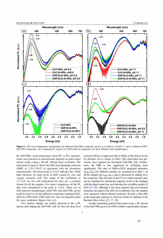
the ZnO-NRs, room-temperature micro-PL (μ-PL) measure-ments were pursued on nanostructure deposits on gold coatedsilicon wafers using a 80 μW, 266 nm laser excitation. Themain peak in figure 4 shows the ZnO near-bandedge emission(NBE) at 3.25–3.38 eV in agreement with the absorptionmeasurements. The broad peak at 2.4 eV indicates the visiblelight emission via deep levels in ZnO caused by zinc andoxygen vacancies [19]. The origin of the oscillations at1.7–2 eV are not well understood but they are a commonfeature for all the samples. For easier comparison, all the PLdata were normalized to the peak at 1.9 eV. Three sets ofZnO-nanorod morphologies (ZnO-NPs and ZnO-NRs grownat pH 6.6 and 11) in four different composites (undoped ZnO,ZnO:Al, GNP/ZnO, GNP/ZnO:Al) were investigated underthe same conditions (figures 4(a)–(c)).
Two distinct changes are readily observed in the μ-PLspectra after doping the ZnO-NRs with Al; first, the deep level
emission (DLE) is suppressed due to filling of the defects levelsby electrons (Al is a donor in ZnO). This observation has pre-viously been reported for Ga-doped ZnO-NRs [26]. Further-more, the NBE is also suppressed by Al-doping moresignificantly. The ratio of NBE-to-DLE integrated intensities(INBE/IDLE) for different samples are summarized in table 1. Inall the samples the INBE/IDLE ratio is decreased by adding Al tothe composite. This decrease in the UV-to-visible emission ratiocan be explained by introducing impurity levels in the bandgapwith the doped metal ions and reducing the crystalline quality ofZnO [27–29]. Although it has been reported that post thermaltreatment can improve the ZnO:Al crystallinity [28], our sampleswere measured without thermal treatment. Second, a blue-shiftin the band-edge emission is observed which we attribute to theBurstein–Moss effect [23, 27, 30].
Another interesting general observation in the μ-PL spectrais that ZnO-NRs grown on GNPs exhibit a significantly stronger
Figure 4. μ-PL room-temperature measurement for different ZnO-NRs composites grown at (a) pH 6.6, (b) pH 11, and (c) different GNP/ZnO-NPs composites. (d) Comparing PL spectra for GNP/ZnO:Al composites for three different ZnO morphologies.
5
Nanotechnology 29 (2018) 415201 E Chalangar et al
97
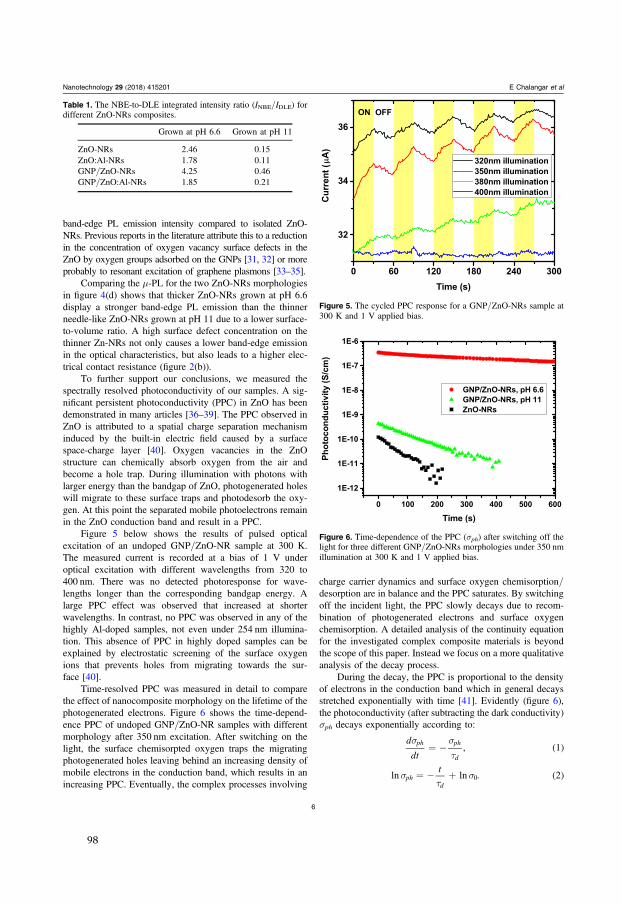
band-edge PL emission intensity compared to isolated ZnO-NRs. Previous reports in the literature attribute this to a reductionin the concentration of oxygen vacancy surface defects in theZnO by oxygen groups adsorbed on the GNPs [31, 32] or moreprobably to resonant excitation of graphene plasmons [33–35].
Comparing the μ-PL for the two ZnO-NRs morphologiesin figure 4(d) shows that thicker ZnO-NRs grown at pH 6.6display a stronger band-edge PL emission than the thinnerneedle-like ZnO-NRs grown at pH 11 due to a lower surface-to-volume ratio. A high surface defect concentration on thethinner Zn-NRs not only causes a lower band-edge emissionin the optical characteristics, but also leads to a higher elec-trical contact resistance (figure 2(b)).
To further support our conclusions, we measured thespectrally resolved photoconductivity of our samples. A sig-nificant persistent photoconductivity (PPC) in ZnO has beendemonstrated in many articles [36–39]. The PPC observed inZnO is attributed to a spatial charge separation mechanisminduced by the built-in electric field caused by a surfacespace-charge layer [40]. Oxygen vacancies in the ZnOstructure can chemically absorb oxygen from the air andbecome a hole trap. During illumination with photons withlarger energy than the bandgap of ZnO, photogenerated holeswill migrate to these surface traps and photodesorb the oxy-gen. At this point the separated mobile photoelectrons remainin the ZnO conduction band and result in a PPC.
Figure 5 below shows the results of pulsed opticalexcitation of an undoped GNP/ZnO-NR sample at 300 K.The measured current is recorded at a bias of 1 V underoptical excitation with different wavelengths from 320 to400 nm. There was no detected photoresponse for wave-lengths longer than the corresponding bandgap energy. Alarge PPC effect was observed that increased at shorterwavelengths. In contrast, no PPC was observed in any of thehighly Al-doped samples, not even under 254 nm illumina-tion. This absence of PPC in highly doped samples can beexplained by electrostatic screening of the surface oxygenions that prevents holes from migrating towards the sur-face [40].
Time-resolved PPC was measured in detail to comparethe effect of nanocomposite morphology on the lifetime of thephotogenerated electrons. Figure 6 shows the time-depend-ence PPC of undoped GNP/ZnO-NR samples with differentmorphology after 350 nm excitation. After switching on thelight, the surface chemisorpted oxygen traps the migratingphotogenerated holes leaving behind an increasing density ofmobile electrons in the conduction band, which results in anincreasing PPC. Eventually, the complex processes involving
charge carrier dynamics and surface oxygen chemisorption/desorption are in balance and the PPC saturates. By switchingoff the incident light, the PPC slowly decays due to recom-bination of photogenerated electrons and surface oxygenchemisorption. A detailed analysis of the continuity equationfor the investigated complex composite materials is beyondthe scope of this paper. Instead we focus on a more qualitativeanalysis of the decay process.
During the decay, the PPC is proportional to the densityof electrons in the conduction band which in general decaysstretched exponentially with time [41]. Evidently (figure 6),the photoconductivity (after subtracting the dark conductivity)σph decays exponentially according to:
d
dt, 1
ph ph
d
s st
= - ( )
tln ln . 2ph
d0s
ts= - + ( )
Table 1. The NBE-to-DLE integrated intensity ratio (INBE/IDLE) fordifferent ZnO-NRs composites.
Grown at pH 6.6 Grown at pH 11
ZnO-NRs 2.46 0.15ZnO:Al-NRs 1.78 0.11GNP/ZnO-NRs 4.25 0.46GNP/ZnO:Al-NRs 1.85 0.21
Figure 5. The cycled PPC response for a GNP/ZnO-NRs sample at300 K and 1 V applied bias.
Figure 6. Time-dependence of the PPC (σph) after switching off thelight for three different GNP/ZnO-NRs morphologies under 350 nmillumination at 300 K and 1 V applied bias.
6
Nanotechnology 29 (2018) 415201 E Chalangar et al
98
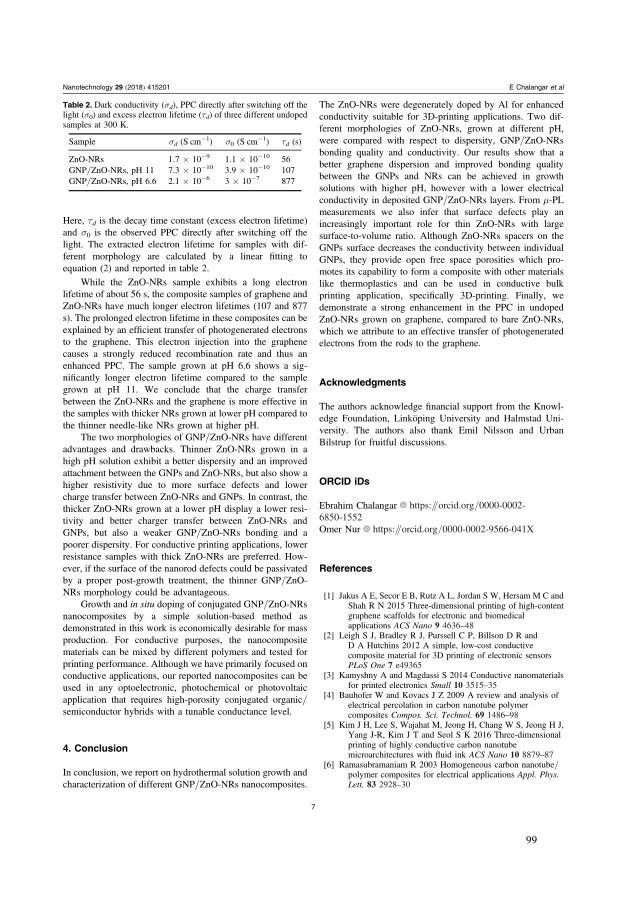
Here, τd is the decay time constant (excess electron lifetime)and σ0 is the observed PPC directly after switching off thelight. The extracted electron lifetime for samples with dif-ferent morphology are calculated by a linear fitting toequation (2) and reported in table 2.
While the ZnO-NRs sample exhibits a long electronlifetime of about 56 s, the composite samples of graphene andZnO-NRs have much longer electron lifetimes (107 and 877s). The prolonged electron lifetime in these composites can beexplained by an efficient transfer of photogenerated electronsto the graphene. This electron injection into the graphenecauses a strongly reduced recombination rate and thus anenhanced PPC. The sample grown at pH 6.6 shows a sig-nificantly longer electron lifetime compared to the samplegrown at pH 11. We conclude that the charge transferbetween the ZnO-NRs and the graphene is more effective inthe samples with thicker NRs grown at lower pH compared tothe thinner needle-like NRs grown at higher pH.
The two morphologies of GNP/ZnO-NRs have differentadvantages and drawbacks. Thinner ZnO-NRs grown in ahigh pH solution exhibit a better dispersity and an improvedattachment between the GNPs and ZnO-NRs, but also show ahigher resistivity due to more surface defects and lowercharge transfer between ZnO-NRs and GNPs. In contrast, thethicker ZnO-NRs grown at a lower pH display a lower resi-tivity and better charger transfer between ZnO-NRs andGNPs, but also a weaker GNP/ZnO-NRs bonding and apoorer dispersity. For conductive printing applications, lowerresistance samples with thick ZnO-NRs are preferred. How-ever, if the surface of the nanorod defects could be passivatedby a proper post-growth treatment, the thinner GNP/ZnO-NRs morphology could be advantageous.
Growth and in situ doping of conjugated GNP/ZnO-NRsnanocomposites by a simple solution-based method asdemonstrated in this work is economically desirable for massproduction. For conductive purposes, the nanocompositematerials can be mixed by different polymers and tested forprinting performance. Although we have primarily focused onconductive applications, our reported nanocomposites can beused in any optoelectronic, photochemical or photovoltaicapplication that requires high-porosity conjugated organic/semiconductor hybrids with a tunable conductance level.
4. Conclusion
In conclusion, we report on hydrothermal solution growth andcharacterization of different GNP/ZnO-NRs nanocomposites.
The ZnO-NRs were degenerately doped by Al for enhancedconductivity suitable for 3D-printing applications. Two dif-ferent morphologies of ZnO-NRs, grown at different pH,were compared with respect to dispersity, GNP/ZnO-NRsbonding quality and conductivity. Our results show that abetter graphene dispersion and improved bonding qualitybetween the GNPs and NRs can be achieved in growthsolutions with higher pH, however with a lower electricalconductivity in deposited GNP/ZnO-NRs layers. From μ-PLmeasurements we also infer that surface defects play anincreasingly important role for thin ZnO-NRs with largesurface-to-volume ratio. Although ZnO-NRs spacers on theGNPs surface decreases the conductivity between individualGNPs, they provide open free space porosities which pro-motes its capability to form a composite with other materialslike thermoplastics and can be used in conductive bulkprinting application, specifically 3D-printing. Finally, wedemonstrate a strong enhancement in the PPC in undopedZnO-NRs grown on graphene, compared to bare ZnO-NRs,which we attribute to an effective transfer of photogeneratedelectrons from the rods to the graphene.
Acknowledgments
The authors acknowledge financial support from the Knowl-edge Foundation, Linköping University and Halmstad Uni-versity. The authors also thank Emil Nilsson and UrbanBilstrup for fruitful discussions.
ORCID iDs
Ebrahim Chalangar https://orcid.org/0000-0002-6850-1552Omer Nur https://orcid.org/0000-0002-9566-041X
References
[1] Jakus A E, Secor E B, Rutz A L, Jordan S W, Hersam M C andShah R N 2015 Three-dimensional printing of high-contentgraphene scaffolds for electronic and biomedicalapplications ACS Nano 9 4636–48
[2] Leigh S J, Bradley R J, Purssell C P, Billson D R andD A Hutchins 2012 A simple, low-cost conductivecomposite material for 3D printing of electronic sensorsPLoS One 7 e49365
[3] Kamyshny A and Magdassi S 2014 Conductive nanomaterialsfor printed electronics Small 10 3515–35
[4] Bauhofer W and Kovacs J Z 2009 A review and analysis ofelectrical percolation in carbon nanotube polymercomposites Compos. Sci. Technol. 69 1486–98
[5] Kim J H, Lee S, Wajahat M, Jeong H, Chang W S, Jeong H J,Yang J-R, Kim J T and Seol S K 2016 Three-dimensionalprinting of highly conductive carbon nanotubemicroarchitectures with fluid ink ACS Nano 10 8879–87
[6] Ramasubramaniam R 2003 Homogeneous carbon nanotube/polymer composites for electrical applications Appl. Phys.Lett. 83 2928–30
Table 2. Dark conductivity (σd), PPC directly after switching off thelight (σ0) and excess electron lifetime (τd) of three different undopedsamples at 300 K.
Sample σd (S cm−1) σ0 (S cm−1) τd (s)
ZnO-NRs 1.7×10⁻⁹ 1.1×10⁻¹⁰ 56GNP/ZnO-NRs, pH 11 7.3×10⁻¹⁰ 3.9×10⁻¹⁰ 107GNP/ZnO-NRs, pH 6.6 2.1×10⁻⁶ 3×10⁻⁷ 877
7
Nanotechnology 29 (2018) 415201 E Chalangar et al
99
[7] Weiss N O, Zhou H, Liao L, Liu Y, Jiang S, Huang Y andDuan X 2012 Graphene: an emerging electronic materialAdv. Mater. 24 5782–825
[8] Li D, Muller M B, Gilje S, Kaner R B and Wallace G G 2008Processable aqueous dispersions of graphene nanosheetsNat. Nanotechnol. 3 101–5
[9] Arapov K, Rubingh E, Abbel R, Laven J, de With G andFriedrich H 2016 Conductive screen printing inks bygelation of graphene dispersions Adv. Funct. Mater. 26586–93
[10] Gao N and Fang X 2015 Synthesis and development ofgraphene inorganic semiconductor nanocomposites Chem.Rev. 115 8294–343
[11] Klingshirn C, Fallert J, Zhou H, Sartor J, Thiele C,Maier-Flaig F, Schneider D and Kalt H 2010 65 years ofZnO research old and very recent results Phys. Status Solidib 247 1424–47
[12] Willander M et al 2009 Zinc oxide nanorod based photonicdevices: recent progress in growth, light emitting diodes andlasers Nanotechnology 20 332001
[13] Amin G, Asif M H, Zainelabdin A, Zaman S, Nur O andWillander M 2011 Influence of pH, precursor concentration,growth time, and temperature on the morphology of ZnOnanostructures grown by the hydrothermal methodJ. Nanomater. 2011 5:5
[14] Munshi A M, Dheeraj D L, Fauske V T, Kim D-C,van Helvoort A T J, Fimland B-O and Weman H 2012Vertically aligned GaAs nanowires on graphite and few-layer graphene: generic model and epitaxial growth NanoLett. 12 4570–6
[15] Larson K, Clark A, Appel A, Dai Q, He H and Zygmunt S2015 Surface-dependence of interfacial bindingstrength between zinc oxide and graphene RSC Adv. 565719–24
[16] Choi W M, Shin K-S, Lee H S, Choi D, Kim K, Shin H-J,Yoon S-M, Choi J-Y and Kim S-W 2011 Selective growthof ZnO nanorods on SiO2/Si substrates using a graphenebuffer layer Nano Res. 4 440–7
[17] Lin J, Penchev M, Wang G, Paul R K, Zhong J, Jing X,Ozkan M and Ozkan C S 2010 Heterogeneous graphenenanostructures: ZnO nanostructures grown on large-areagraphene layers Small 6 2448–52
[18] Hwang J O, Lee D H, Kim J Y, Han T H, Kim B H, Park M,No K and Kim S O 2011 Vertical ZnO nanowires/graphenehybrids for transparent and flexible field emission J. Mater.Chem. 21 3432–7
[19] Alnoor H, Pozina G, Khranovskyy V, Liu X, Iandolo D,Willander M and Nur O 2016 Influence of ZnO seed layerprecursor molar ratio on the density of interface defects inlow temperature aqueous chemically synthesized ZnOnanorods/GaN light-emitting diodes J. Appl. Phys. 119165702
[20] Brsan O A, Hoffmann G G, van der Ven L G J and de With G2016 Single-walled carbon nanotube networks: the influenceof individual tube–tube contacts on the large-scaleconductivity of polymer composites Adv. Funct. Mater. 264377–85
[21] Fuchs P, Hagendorfer H, Romanyuk Y E and Tiwari A N 2015Doping strategies for highly conductive Al-doped ZnO filmsgrown from aqueous solution Phys. Status Solidi a 212 51–5
[22] Miyake M, Fukui H and Hirato T 2012 Preparation of Al-doped ZnO films by aqueous solution process using acontinuous circulation reactor Phys. Status Solidi a 209945–8
[23] Edinger S, Bansal N, Bauch M, Wibowo R A, Hamid R,Trimmel G and Dimopoulos T 2017 Comparison of
chemical bath-deposited ZnO films doped with Al, Ga andIn J. Mater. Sci. 52 9410–23
[24] Chandraiahgari C R, De Bellis G, Balijepalli S K, Kaciulis S,Ballirano P, Migliori A, Morandi V, Caneve L, Sarto F andSarto M S 2016 Control of the size and density of ZnO-nanorods grown onto graphene nanoplatelets in aqueoussuspensions RSC Adv. 6 83217–25
[25] Podbrek P, Drai G, Paramo J A, Strzhemechny Y M,Maek J and Orel Z C 2010 Growth of zinc oxide particles inthe presence of silicon CrystEngComm 12 3071–9
[26] Sakurai M, Wang Y G, Uemura T and Aono M 2009 Electricalproperties of individual ZnO nanowires Nanotechnology 20155203
[27] Zhu Q, Xie C, Li H, Yang C, Zhang S and Zeng D 2014Selectively enhanced UV and NIR photoluminescence froma degenerate ZnO nanorod array film J. Mater. Chem. C 24566–80
[28] Wang M, Lee K E, Hahn S H, Kim E J, Kim S, Chung J S,Shin E W and Park C 2007 Optical and photoluminescentproperties of sol-gel Al-doped ZnO thin filmsMater. Lett. 611118–21
[29] Rahman M M, Khan M K R, Rafiqul Islam M, Halim M A,Shahjahan M, Hakim M A, Saha D K and Khan J U 2012Effect of Al doping on structural, electrical, optical andphotoluminescence properties of nano-structural ZnO thinfilms J. Mater. Sci. Technol. 28 329–35
[30] Ziabari A A and Rozati S M 2012 Carrier transport andbandgap shift in n-type degenerate ZnO thin films: the effectof band edge nonparabolicity Physica B 407 4512–7
[31] Lee E, Kim J-Y, Kwon B J, Jang E-S and An S J 2014Vacancy filling effect of graphene on photoluminescencebehavior of ZnO/graphene nanocomposite Phys. StatusSolidi 8 836–40
[32] Pham C V, Repp S, Thomann R, Krueger M, Weber S andErdem E 2016 Charge transfer and surface defect healingwithin ZnO nanoparticle decorated graphene hybridmaterials Nanoscale 8 9682–7
[33] Hwang S W et al 2010 Plasmon-enhanced ultravioletphotoluminescence from hybrid structures of graphene/ZnOfilms Phys. Rev. Lett. 105 127403
[34] Zhang S G, Wen L, Li J L, Gao F L, Zhang X W, Li L H andLi G Q 2014 Plasmon-enhanced ultravioletphotoluminescence from highly ordered ZnO nanorods/graphene hybrid structure decorated with Au nanospheresJ. Phys. D: Appl. Phys. 47 495103
[35] Liu R, Fu X-W, Meng J, Bie Y-Q, Yu D-P and Liao Z-M 2013Graphene plasmon enhanced photoluminescence in ZnOmicrowires Nanoscale 5 5294–8
[36] Medved D B 1961 Photoconductivity and chemisorptionkinetics in sintered zinc oxide semiconductor J. Phys. Chem.Solids 20 255–67
[37] Chen M-W, Chen C-Y, Lien D-H, Ding Y and He J-H 2010Photoconductive enhancement of single ZnO nanowire throughlocalized Schottky effects Opt. Express 18 14836–41
[38] Moore J C and C V Thompson 2013 A phenomenologicalmodel for the photocurrent transient relaxation observed inZnO-based photodetector devices Sensors 13 9921–40
[39] Zhu Q, Xie C, Li H, Zhang J and Zeng D 2015 Through-processanalytical modeling of photoconductance spectrum for porousZnO nanocrystalline film Chem. Mater. 27 2861–74
[40] Zhu Q, Xie C, Li H and Zeng D 2016 A method for modeling anddeciphering the persistent photoconductance and long-termcharge storage of ZnO nanorod arrays Nano Res. 9 2972–3002
[41] Rani M and Tripathi S K 2016 Electron transfer properties oforganic dye sensitized ZnO and ZnO/TiO2 photoanode for dyesensitized solar cells Renew. Sustain. Energy Rev. 61 97–107
8
Nanotechnology 29 (2018) 415201 E Chalangar et al
100

II PAPER
101

102
Graphene-based plasmonic nanocomposites forhighly enhanced solar-driven photocatalyticactivities
Rania E. Adam, †*a Ebrahim Chalangar, †ab Mahsa Pirhashemi,c Galia Pozina,d
Xianjie Liu,d Justinas Palisaitis,d Hakan Pettersson,abe Magnus Willandera
and Omer Nur a
High-efficiency photocatalysts are crucial for the removal of organic pollutants and environmental
sustainability. In the present work, we report on a new low-temperature hydrothermal chemical method,
assisted by ultrasonication, to synthesize disruptive plasmonic ZnO/graphene/Ag/AgI nanocomposites
for solar-driven photocatalysis. The plasmonic nanocomposites were investigated by a wide range of
characterization techniques, confirming successful formation of photocatalysts with excellent
degradation efficiency. Using Congo red as a model dye molecule, our experimental results
demonstrated a photocatalytic reactivity exceeding 90% efficiency after one hour simulated solar
irradiation. The significantly enhanced degradation efficiency is attributed to improved electronic
properties of the nanocomposites by hybridization of the graphene and to the addition of Ag/AgI which
generates a strong surface plasmon resonance effect in the metallic silver further improving the
photocatalytic activity and stability under solar irradiation. Scavenger experiments suggest that
superoxide and hydroxyl radicals are responsible for the photodegradation of Congo red. Our findings
are important for the fundamental understanding of the photocatalytic mechanism of ZnO/graphene/Ag/
AgI nanocomposites and can lead to further development of novel efficient photocatalyst materials.
1 Introduction
Research on solar energy-driven photocatalysts is growing fastdue to environmental concerns and to the need for utilization ofsustainable energy resources.1–4 So far, semiconductor-basednanostructures are among the most studied materials for pho-tocatalytic purposes due to their remarkably high efficiency.5–9
However, many of these semiconductors suffer from issues withpoor absorption of light and high recombination rates of pho-togenerated electron–hole (e�/h+) pairs.1,10 Heterostructurematerials offer the possibility of advanced bandgap engineeringto drastically improve the scavenging of energy from thesunlight for degradation of harmful organic compounds andcontaminants. Various heterostructure materials have been
explored with the aim to nd materials with enhanced photo-catalytic properties under solar light irradiation. Zinc oxide(ZnO) is a remarkable photocatalyst that can be compositedwith other materials to improve visible light harvesting and,thus, the photocatalytic efficiency. ZnO–graphene nano-composites are particularly interesting heterostructures witha capability of inhibiting the recombination of photogeneratedcharge carriers during the photocatalytic process. Graphene(GR) is a well-known 2D material consisting of carbon atomsarranged in a honeycomb lattice structure.11,12 It possessesmany fundamentally interesting electronic properties such aszero bandgap, zero effective mass, high charge carrier mobility,large surface area, and high optical transparency over a verylarge spectral range from IR to UV, which makes it an excellentcandidate for enhancing the performance of photo-catalysts.10,11,13–15 It was found that GR and GR oxide cansignicantly improve the separation efficiency of photo-generated e�/h+ pairs in photocatalytic processes.10,11,16–20 Forinstance, Tian et al.21 fabricated ZnO nanorods/reduced GRoxide nanocomposites for enhancing the photodegradation ofmethylene blue dye. Also, Sawant et al.22 showed an enhance-ment of the photodegradation capability of methylene orangeand rhodamine B using ZnO/GR nanosheets.
Many different metal–semiconductor nanostructures havebeen studied as plasmonic photocatalysts.6,23,24 Recently, Ag-
aDepartment of Sciences and Technology, Linkoping University, Campus Norrkoping,
SE-601 74 Norrkoping, Sweden. E-mail: [email protected] of Information Technology, Halmstad University, SE-301 18 Halmstad,
SwedencDepartment of Chemistry, Faculty of Sciences, University of Mohaghegh Ardabili, P.O.
Box 179, Ardabil, IrandDepartment of Physics, Chemistry, and Biology (IFM), Linkoping University, 58183
Linkoping, SwedeneSolid State Physics and NanoLund, Lund University, SE-221 00 Lund, Sweden
† Both have contributed equally to the work and should be considered co-rstauthors.
Cite this: RSC Adv., 2019, 9, 30585
Received 12th August 2019Accepted 19th September 2019
DOI: 10.1039/c9ra06273d
rsc.li/rsc-advances
This journal is © The Royal Society of Chemistry 2019
RSC Advances
PAPER View Article OnlineView Journal | View Issue
103
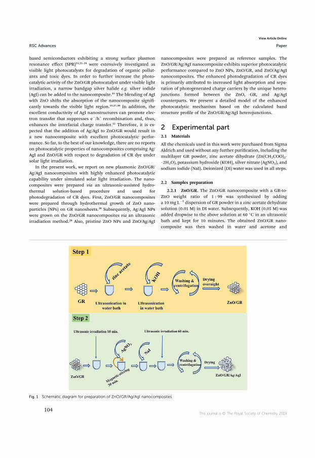
based semiconductors exhibiting a strong surface plasmonresonance effect (SPR)23,25–29 were extensively investigated asvisible light photocatalysts for degradation of organic pollut-ants and toxic dyes. In order to further increase the photo-catalytic activity of the ZnO/GR photocatalyst under visible lightirradiation, a narrow bandgap silver halide e.g. silver iodide(AgI) can be added to the nanocomposite.25 The blending of AgIwith ZnO shis the absorption of the nanocomposite signi-cantly towards the visible light region.11,27,30 In addition, theexcellent conductivity of AgI nanostructures can promote elec-tron transfer that suppresses e�/h+ recombination and, thus,enhances the interfacial charge transfer.25 Therefore, it is ex-pected that the addition of Ag/AgI to ZnO/GR would result ina new nanocomposite with excellent photocatalytic perfor-mance. So far, to the best of our knowledge, there are no reportson photocatalytic properties of nanocomposites comprising Ag/AgI and ZnO/GR with respect to degradation of CR dye undersolar light irradiation.
In the present work, we report on new plasmonic ZnO/GR/Ag/AgI nanocomposites with highly enhanced photocatalyticcapability under simulated solar light irradiation. The nano-composites were prepared via an ultrasonic-assisted hydro-thermal solution-based procedure and used forphotodegradation of CR dyes. First, ZnO/GR nanocompositeswere prepared through hydrothermal growth of ZnO nano-particles (NPs) on GR nanosheets.20 Subsequently, Ag/AgI NPswere grown on the ZnO/GR nanocomposites via an ultrasonicirradiation method.20 Also, pristine ZnO NPs and ZnO/Ag/AgI
nanocomposites were prepared as reference samples. TheZnO/GR/Ag/AgI nanocomposite exhibits superior photocatalyticperformance compared to ZnO NPs, ZnO/GR, and ZnO/Ag/AgInanocomposites. The enhanced photodegradation of CR dyesis primarily attributed to increased light absorption and sepa-ration of photogenerated charge carriers by the unique hetero-junctions formed between the ZnO, GR, and Ag/AgIcounterparts. We present a detailed model of the enhancedphotocatalytic mechanism based on the calculated bandstructure prole of the ZnO/GR/Ag/AgI heterojunctions.
2 Experimental part2.1 Materials
All the chemicals used in this work were purchased from SigmaAldrich and used without any further purication, including themultilayer GR powder, zinc acetate dihydrate (Zn(CH3COO)2-$2H2O), potassium hydroxide (KOH), silver nitrate (AgNO3), andsodium iodide (NaI). Deionized (DI) water was used in all steps.
2.2 Samples preparation
2.2.1 ZnO/GR. The ZnO/GR nanocomposite with a GR-to-ZnO weight ratio of 1 : 99 was synthesized by addinga 10 mg L�1 dispersion of GR powder in a zinc acetate dehydratesolution (0.01 M) in DI water. Subsequently, KOH (0.05 M) wasadded dropwise to the above solution at 60 �C in an ultrasonicbath and kept for 10 minutes. The obtained ZnO/GR nano-composite was then washed in water and acetone and
Fig. 1 Schematic diagram for preparation of ZnO/GR/Ag/AgI nanocomposites.
This journal is © The Royal Society of Chemistry 2019
RSC Advances Paper
View Article Online
104
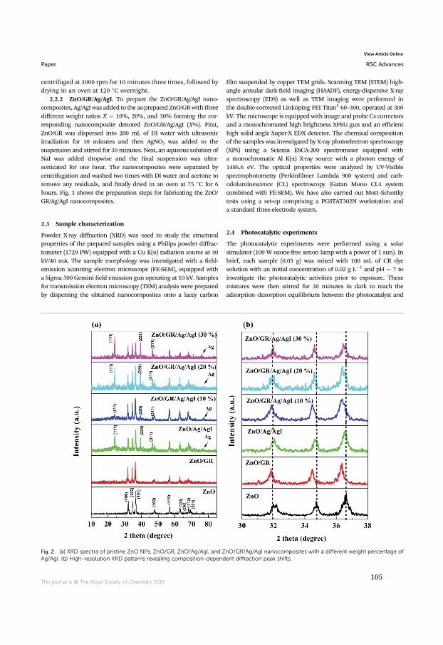
centrifuged at 3000 rpm for 10 minutes three times, followed bydrying in an oven at 120 �C overnight.
2.2.2 ZnO/GR/Ag/AgI. To prepare the ZnO/GR/Ag/AgI nano-composites, Ag/AgI was added to the as-prepared ZnO/GRwith threedifferent weight ratios X ¼ 10%, 20%, and 30% forming the cor-responding nanocomposite denoted ZnO/GR/Ag/AgI (X%). First,ZnO/GR was dispersed into 200 mL of DI water with ultrasonicirradiation for 10 minutes and then AgNO3 was added to thesuspension and stirred for 30minutes. Next, an aqueous solution ofNaI was added dropwise and the nal suspension was ultra-sonicated for one hour. The nanocomposites were separated bycentrifugation and washed two times with DI water and acetone toremove any residuals, and nally dried in an oven at 75 �C for 6hours. Fig. 1 shows the preparation steps for fabricating the ZnO/GR/Ag/AgI nanocomposites.
2.3 Sample characterization
Powder X-ray diffraction (XRD) was used to study the structuralproperties of the prepared samples using a Philips powder diffrac-tometer (1729 PW) equipped with a Cu K(a) radiation source at 40kV/40 mA. The sample morphology was investigated with a eld-emission scanning electron microscope (FE-SEM), equipped witha Sigma 500 Gemini eld emission gun operating at 10 kV. Samplesfor transmission electron microscopy (TEM) analysis were preparedby dispersing the obtained nanocomposites onto a lacey carbon
lm suspended by copper TEM grids. Scanning TEM (STEM) high-angle annular dark-eld imaging (HAADF), energy-dispersive X-rayspectroscopy (EDS) as well as TEM imaging were performed inthe double-corrected Linkoping FEI Titan3 60–300, operated at 300kV. Themicroscope is equippedwith image and probeCs correctorsand a monochromated high brightness XFEG gun and an efficienthigh solid angle Super-X EDX detector. The chemical compositionof the samples was investigated by X-ray photoelectron spectroscopy(XPS) using a Scienta ESCA-200 spectrometer equipped witha monochromatic Al K(a) X-ray source with a photon energy of1486.6 eV. The optical properties were analyzed by UV-Visiblespectrophotometry (PerkinElmer Lambda 900 system) and cath-odoluminescence (CL) spectroscopy (Gatan Mono CL4 systemcombined with FE-SEM). We have also carried out Mott–Schottkytests using a set-up comprising a PGSTAT302N workstation anda standard three-electrode system.
2.4 Photocatalytic experiments
The photocatalytic experiments were performed using a solarsimulator (100 W ozone-free xenon lamp with a power of 1 sun). Inbrief, each sample (0.05 g) was mixed with 100 mL of CR dyesolution with an initial concentration of 0.02 g L�1 and pH � 7 toinvestigate the photocatalytic activities prior to exposure. Thesemixtures were then stirred for 30 minutes in dark to reach theadsorption–desorption equilibrium between the photocatalyst and
Fig. 2 (a) XRD spectra of pristine ZnO NPs, ZnO/GR, ZnO/Ag/AgI, and ZnO/GR/Ag/AgI nanocomposites with a different weight percentage ofAg/AgI. (b) High-resolution XRD patterns revealing composition-dependent diffraction peak shifts.
This journal is © The Royal Society of Chemistry 2019
Paper RSC Advances
View Article Online
105
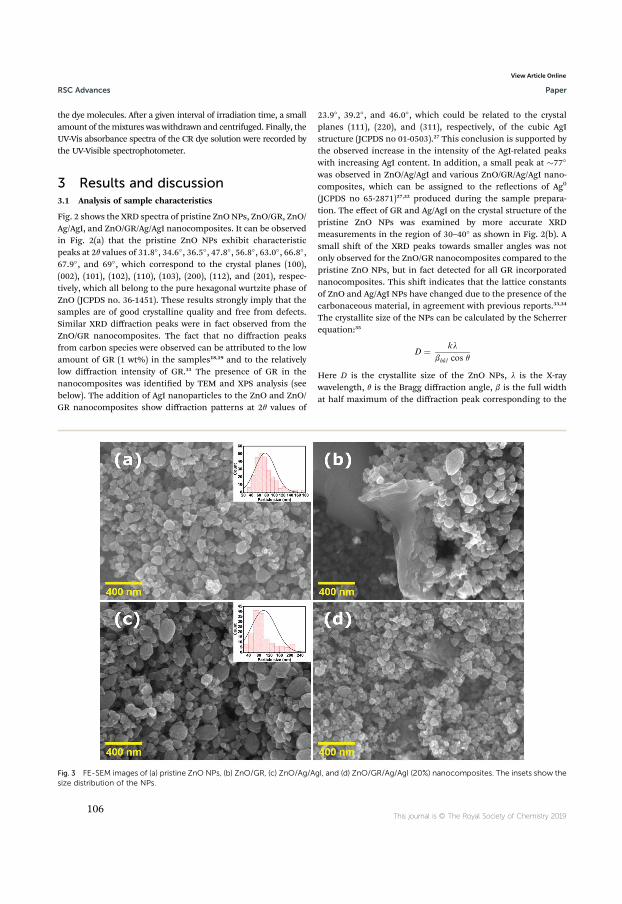
the dye molecules. Aer a given interval of irradiation time, a smallamount of themixtures was withdrawn and centrifuged. Finally, theUV-Vis absorbance spectra of the CR dye solution were recorded bythe UV-Visible spectrophotometer.
3 Results and discussion3.1 Analysis of sample characteristics
Fig. 2 shows the XRD spectra of pristine ZnONPs, ZnO/GR, ZnO/Ag/AgI, and ZnO/GR/Ag/AgI nanocomposites. It can be observedin Fig. 2(a) that the pristine ZnO NPs exhibit characteristicpeaks at 2q values of 31.8�, 34.6�, 36.5�, 47.8�, 56.8�, 63.0�, 66.8�,67.9�, and 69�, which correspond to the crystal planes (100),(002), (101), (102), (110), (103), (200), (112), and (201), respec-tively, which all belong to the pure hexagonal wurtzite phase ofZnO (JCPDS no. 36-1451). These results strongly imply that thesamples are of good crystalline quality and free from defects.Similar XRD diffraction peaks were in fact observed from theZnO/GR nanocomposites. The fact that no diffraction peaksfrom carbon species were observed can be attributed to the lowamount of GR (1 wt%) in the samples18,19 and to the relativelylow diffraction intensity of GR.31 The presence of GR in thenanocomposites was identied by TEM and XPS analysis (seebelow). The addition of AgI nanoparticles to the ZnO and ZnO/GR nanocomposites show diffraction patterns at 2q values of
23.9�, 39.2�, and 46.0�, which could be related to the crystalplanes (111), (220), and (311), respectively, of the cubic AgIstructure (JCPDS no 01-0503).27 This conclusion is supported bythe observed increase in the intensity of the AgI-related peakswith increasing AgI content. In addition, a small peak at �77�
was observed in ZnO/Ag/AgI and various ZnO/GR/Ag/AgI nano-composites, which can be assigned to the reections of Ag0
(JCPDS no 65-2871)27,32 produced during the sample prepara-tion. The effect of GR and Ag/AgI on the crystal structure of thepristine ZnO NPs was examined by more accurate XRDmeasurements in the region of 30–40� as shown in Fig. 2(b). Asmall shi of the XRD peaks towards smaller angles was notonly observed for the ZnO/GR nanocomposites compared to thepristine ZnO NPs, but in fact detected for all GR incorporatednanocomposites. This shi indicates that the lattice constantsof ZnO and Ag/AgI NPs have changed due to the presence of thecarbonaceous material, in agreement with previous reports.33,34
The crystallite size of the NPs can be calculated by the Scherrerequation:35
D ¼ kl
bhkl cos q
Here D is the crystallite size of the ZnO NPs, l is the X-raywavelength, q is the Bragg diffraction angle, b is the full widthat half maximum of the diffraction peak corresponding to the
Fig. 3 FE-SEM images of (a) pristine ZnO NPs, (b) ZnO/GR, (c) ZnO/Ag/AgI, and (d) ZnO/GR/Ag/AgI (20%) nanocomposites. The insets show thesize distribution of the NPs.
This journal is © The Royal Society of Chemistry 2019
RSC Advances Paper
View Article Online
106
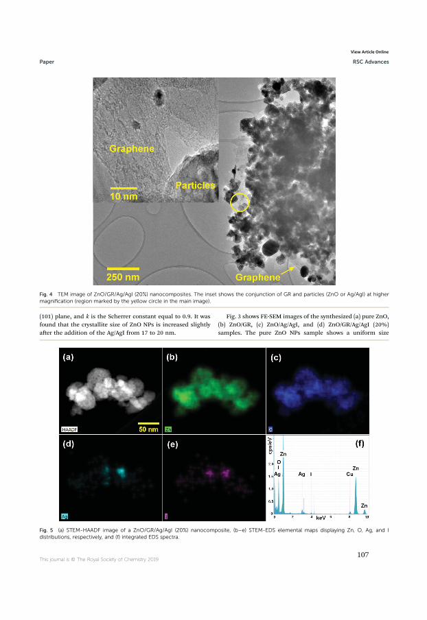
(101) plane, and k is the Scherrer constant equal to 0.9. It wasfound that the crystallite size of ZnO NPs is increased slightlyaer the addition of the Ag/AgI from 17 to 20 nm.
Fig. 3 shows FE-SEM images of the synthesized (a) pure ZnO,(b) ZnO/GR, (c) ZnO/Ag/AgI, and (d) ZnO/GR/Ag/AgI (20%)samples. The pure ZnO NPs sample shows a uniform size
Fig. 4 TEM image of ZnO/GR/Ag/AgI (20%) nanocomposites. The inset shows the conjunction of GR and particles (ZnO or Ag/AgI) at highermagnification (region marked by the yellow circle in the main image).
Fig. 5 (a) STEM-HAADF image of a ZnO/GR/Ag/AgI (20%) nanocomposite, (b–e) STEM-EDS elemental maps displaying Zn, O, Ag, and Idistributions, respectively, and (f) integrated EDS spectra.
This journal is © The Royal Society of Chemistry 2019
Paper RSC Advances
View Article Online
107
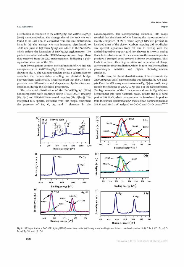
distribution as compared to the ZnO/Ag/AgI and ZnO/GR/Ag/AgI(20%) nanocomposites. The average size of the ZnO NPs wasfound to be �80 nm, as estimated from the size distributioninset in (a). The average NPs size increased signicantly to�100 nm (inset in (c)) when Ag/AgI was added to the ZnO NPs,which reects the formation of ZnO/Ag/AgI agglomerates. Theparticle size observed in the FE-SEM images is much larger thanthat extracted from the XRD measurements, indicating a poly-crystalline structure of the NPs.
TEM investigations conrm the conjunction of NPs and GRnanoplatelets in ZnO/GR/Ag/AgI (20%) nanocomposites asshown in Fig. 4. The GR nanoplatelets act as a substructure toassemble the nanoparticles enabling an electrical bridgebetween them. Additionally, it was observed that the GR nano-platelets have different size and shape caused by the ultrasonicirradiation during the synthesis procedures.
The elemental distribution of the ZnO/GR/Ag/AgI (20%)nanocomposites were examined using STEM-HAADF imaging(Fig. 5(a)) and STEM-EDS elemental mapping (Fig. 5(b–e)). Theintegrated EDS spectra, extracted from EDS maps, conrmedthe presence of Zn, O, Ag, and I elements in the
nanocomposites. The corresponding elemental EDS mapsrevealed that the cluster of NPs forming the nanocomposite ismainly composed of ZnO, while Ag/AgI NPs are present inlocalized areas of the cluster. Carbon mapping did not displayany spectral signatures from GR due to overlap with theunderlying carbon support grid (not shown). It is worth notingthat a better distribution of the elements in the nanocompositesprovides a stronger bond between different counterparts. Thisleads to a more efficient generation and separation of chargecarriers under solar irradiation, which in turn leads to excellentphotocatalytic activities and higher photodegradationefficiency.
Furthermore, the chemical oxidation state of the elements in theZnO/GR/Ag/AgI (20%) nanocomposite was identied by XPS anal-ysis. From the XPS survey scan spectrum in Fig. 6(a) we could clearlyidentify the existence of Zn, O, C, Ag, and I in the nanocomposite.The high resolution of the C 1s spectrum shown in Fig. 6(b) wasdeconvoluted into three Gaussian peaks. Besides the C–C bondpeak at 284.79 eV, which demonstrates the introduced impuritiesfrom the surface contamination,36 there are two dominant peaks at285.57 and 288.71 eV assigned to C–O–C and C]O bonds,11,36,37
Fig. 6 XPS spectra for a ZnO/GR/Ag/AgI (20%) nanocomposite. (a) Survey scan, and high resolution core level spectra of (b) C 1s, (c) Zn 2p, (d) O1s, (e) Ag 3d, and (f) I 3d.
This journal is © The Royal Society of Chemistry 2019
RSC Advances Paper
View Article Online
108
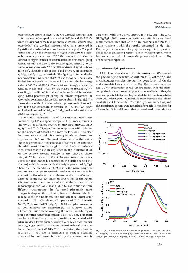
respectively. As shown in Fig. 6(c), the XPS core level spectrum of Zn2p is composed of two peaks centered at 1022.16 and 1045.23 eV,which are ascribed to the binding energy of Zn 2p3/2 and Zn 2p1/2respectively.38 The core-level spectrum of O 1s is presented inFig. 6(d) and it is divided into two Gaussian tted peaks. The peakcentered at 530.50 eV corresponds to oxygen in the ZnO NPs latticein the nanocomposite structure.37,39,40 The peak at 532.37 eV can beascribed to oxygen bonded to carbon atoms (the functional grouppresent on GR) and also to the hydroxyl group adhering to thesurface of nanocomposite.41,42 The XPS spectrum of Ag 3d is shownin Fig. 6(e). Themain peaks at 368.13 and 374.06 eV are assigned toAg 3d5/2 and Ag 3d3/2, respectively. The Ag 3d5/2 is further dividedinto two peaks at 367.82 and 368.28 eV and the Ag 3d3/2 peak is alsodivided into two peaks at 373.79 and 374.32 eV. The low energypeaks at 367.82 and 373.79 eV are attributed to Ag+, whereas thepeaks at 368.28 and 374.32 eV are related to metallic Ag0.27,43
Accordingly, metallic Ag0 is produced at the surface of the ZnO/GR/Ag/AgI (20%) photocatalyst during the sample preparation, anobservation consistent with the XRD results shown in Fig. 2(a). Thechemical state of the I element, which is present in the form of I�
ions in the nanocomposite, is revealed in Fig. 6(f). Two clearlyresolved peaks related to I 3d5/2 and I 3d3/2 are located at 619.02 and630.58 eV, respectively.30
The optical characteristics of the nanocomposites wereexamined by UV-Vis spectroscopy and CL measurements.The UV-Vis absorbance spectra of ZnO NPs, ZnO/GR, ZnO/Ag/AgI, and ZnO/GR/Ag/AgI nanocomposites with differentweight percent of Ag/AgI are shown in Fig. 7(a). It is clearthat pure ZnO NPs exhibit a strong interband absorptionedge around 400 nm. The weak absorbance in the visibleregion is attributed to the presence of native point defects.29
The addition of GR to ZnO slightly redshis the absorbanceedge. This redshi can be explained by the inuence of GRon the surface electric charge in the ZnO/GR photo-catalyst.10,44 In the case of ZnO/GR/Ag/AgI nanocomposites,a broader absorbance is observed in the visible region (l >400 nm) which increases with the weight percent of Ag/AgI.Therefore, the blending of Ag/AgI into the nanocompositecan increase its photocatalytic performance under solarirradiation. The observed absorbance peak at l ¼ 430 nm isassigned to the surface plasmon absorption of the Ag/AgINPs, indicating the presence of Ag0 at the surface of thenanocomposites.45 As a result, due to contributions fromdifferent counterparts, the fabricated plasmonic nano-composite displays the highest optical absorbance, which isbenecial for the photocatalytic performance under solarirradiation. Fig. 7(b) shows CL spectra of ZnO, ZnO/GR,ZnO/Ag/AgI, and ZnO/GR/Ag/AgI (20%) samples, measuredat room temperature. Interestingly, all samples exhibita broad emission band covering the whole visible regionwith a luminescence peak centered at �600 nm. This bandcan be attributed to radiative transitions associated withintrinsic deep levels such as oxygen vacancies and intersti-tials (VO, Oi), as well as to the presence of hydroxyl groups atthe surface of the ZnO NPs.46–48 In addition, the observedpeak at l ¼ 430 nm is attributed to surface plasmon-enhanced luminescence, induced by the Ag/AgI NPs, in
agreement with the UV-Vis spectrum in Fig. 7(a). The ZnO/GR/Ag/AgI (20%) nanocomposite exhibits broader bandluminescence than that of the pure ZnO NPs and ZnO/GR,again consistent with the results presented in Fig. 7(a).Evidently, the presence of Ag/AgI has a signicant positiveeffect on the emission properties in the visible region, whichin turn is expected to improve the photocatalytic capabilityof the nanocomposite.
3.2 Photocatalytic performance
3.2.1 Photodegradation of toxic wastewater. We studiedthe photocatalytic activities of ZnO, ZnO/GR, ZnO/Ag/AgI andZnO/GR/Ag/AgI samples through the degradation of CR dyeunder simulated solar irradiation. Fig. 8(a–f) shows the recor-ded UV-Vis absorbance of the CR dye mixed with the nano-composite in 15 min steps of up to 60 min irradiation. First, thenanocomposite/CR dye was kept in dark for 30 min to reach theadsorption–desorption equilibrium state between the photo-catalysts and CR molecules. Then the light was turned on, andthe absorbance spectra were recorded aer each 15 min step forall samples. It is well-known that carbon-based materials have
Fig. 7 (a) UV-Vis absorbance spectra of pristine ZnO NPs, ZnO/GR,ZnO/Ag/AgI, and ZnO/GR/Ag/AgI nanocomposites with a differentweight percentage of Ag/AgI, and (b) corresponding CL spectra.
This journal is © The Royal Society of Chemistry 2019
Paper RSC Advances
View Article Online
109
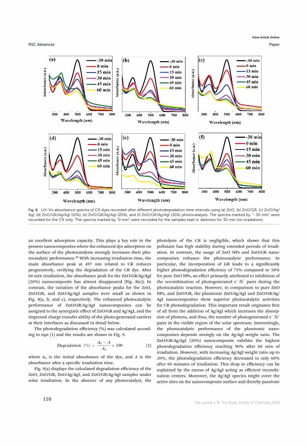
an excellent adsorption capacity. This plays a key role in thepresent nanocomposites where the enhanced dye adsorption onthe surface of the photocatalysts strongly increases their pho-tocatalytic performance.49 With increasing irradiation time, themain absorbance peak at 497 nm related to CR reducesprogressively, verifying the degradation of the CR dye. Aer60 min irradiation, the absorbance peak for the ZnO/GR/Ag/AgI(20%) nanocomposite has almost disappeared (Fig. 8(e)). Incontrast, the variation of the absorbance peaks for the ZnO,ZnO/GR, and ZnO/Ag/AgI samples were small as shown inFig. 8(a, b, and c), respectively. The enhanced photocatalyticperformance of ZnO/GR/Ag/AgI nanocomposites can beassigned to the synergistic effect of ZnO/GR and Ag/AgI, and theimproved charge transfer ability of the photo-generated carriersat their interfaces as discussed in detail below.
The photodegradation efficiency (%) was calculated accord-ing to eqn (1) and the results are shown in Fig. 9.
Degradation ð%Þ ¼ A0 � A
A0
� 100 (1)
where A0 is the initial absorbance of the dye, and A is theabsorbance aer a specic irradiation time.
Fig. 9(a) displays the calculated degradation efficiency of theZnO, ZnO/GR, ZnO/Ag/AgI, and ZnO/GR/Ag/AgI samples undersolar irradiation. In the absence of any photocatalyst, the
photolysis of the CR is negligible, which shows that thispollutant has high stability during extended periods of irradi-ation. In contrast, the usage of ZnO NPs and ZnO/GR nano-composites enhance the photocatalytic performance. Inparticular, the incorporation of GR leads to a signicantlyhigher photodegradation efficiency of 75% compared to 58%for pure ZnO NPs, an effect primarily attributed to inhibition ofthe recombination of photogenerated e�/h+ pairs during thephotocatalytic reaction. However, in comparison to pure ZnONPs, and ZnO/GR, the plasmonic ZnO/Ag/AgI and ZnO/GR/Ag/AgI nanocomposites show superior photocatalytic activitiesfor CR photodegradation. This important result originates rstof all from the addition of Ag/AgI which increases the absorp-tion of photons, and thus, the number of photogenerated e�/h+
pairs in the visible region of the solar spectrum. Interestingly,the photocatalytic performance of the plasmonic nano-composites depends strongly on the Ag/AgI weight ratio. TheZnO/GR/Ag/AgI (20%) nanocomposite exhibits the highestphotodegradation efficiency reaching 90% aer 60 min ofirradiation. However, with increasing Ag/AgI weight ratio up to30%, the photodegradation efficiency decreased to only 60%aer 60 minutes of irradiation. This drop in efficiency can beexplained by the excess of Ag/AgI acting as efficient recombi-nation centers. Moreover, the Ag/AgI species might cover theactive sites on the nanocomposite surface and thereby passivate
Fig. 8 UV-Vis absorbance spectra of CR dyes recorded after different photodegradation time intervals using (a) ZnO, (b) ZnO/GR, (c) ZnO/Ag/AgI, (d) ZnO/GR/Ag/AgI (10%), (e) ZnO/GR/Ag/AgI (20%), and (f) ZnO/GR/Ag/AgI (30%) photocatalysts. The spectra marked by “�30 min” wererecorded for the CR only. The spectra marked by “0 min” were recorded for the samples kept in darkness for 30 min (no irradiation).
This journal is © The Royal Society of Chemistry 2019
RSC Advances Paper
View Article Online
110
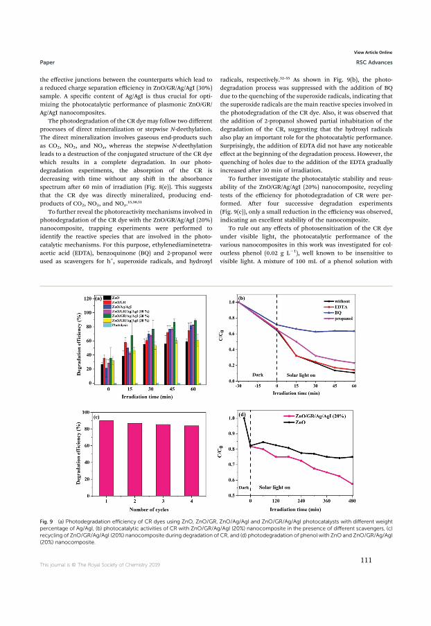
the effective junctions between the counterparts which lead toa reduced charge separation efficiency in ZnO/GR/Ag/AgI (30%)sample. A specic content of Ag/AgI is thus crucial for opti-mizing the photocatalytic performance of plasmonic ZnO/GR/Ag/AgI nanocomposites.
The photodegradation of the CR dyemay follow two differentprocesses of direct mineralization or stepwise N-deethylation.The direct mineralization involves gaseous end-products suchas CO2, NO3, and NOx, whereas the stepwise N-deethylationleads to a destruction of the conjugated structure of the CR dyewhich results in a complete degradation. In our photo-degradation experiments, the absorption of the CR isdecreasing with time without any shi in the absorbancespectrum aer 60 min of irradiation (Fig. 8(e)). This suggeststhat the CR dye was directly mineralized, producing end-products of CO2, NO3, and NOx.15,50,51
To further reveal the photoreactivity mechanisms involved inphotodegradation of the CR dye with the ZnO/GR/Ag/AgI (20%)nanocomposite, trapping experiments were performed toidentify the reactive species that are involved in the photo-catalytic mechanisms. For this purpose, ethylenediaminetetra-acetic acid (EDTA), benzoquinone (BQ) and 2-propanol wereused as scavengers for h+, superoxide radicals, and hydroxyl
radicals, respectively.52–55 As shown in Fig. 9(b), the photo-degradation process was suppressed with the addition of BQdue to the quenching of the superoxide radicals, indicating thatthe superoxide radicals are the main reactive species involved inthe photodegradation of the CR dye. Also, it was observed thatthe addition of 2-propanol showed partial inhabitation of thedegradation of the CR, suggesting that the hydroxyl radicalsalso play an important role for the photocatalytic performance.Surprisingly, the addition of EDTA did not have any noticeableeffect at the beginning of the degradation process. However, thequenching of holes due to the addition of the EDTA graduallyincreased aer 30 min of irradiation.
To further investigate the photocatalytic stability and reus-ability of the ZnO/GR/Ag/AgI (20%) nanocomposite, recyclingtests of the efficiency for photodegradation of CR were per-formed. Aer four successive degradation experiments(Fig. 9(c)), only a small reduction in the efficiency was observed,indicating an excellent stability of the nanocomposite.
To rule out any effects of photosensitization of the CR dyeunder visible light, the photocatalytic performance of thevarious nanocomposites in this work was investigated for col-ourless phenol (0.02 g L�1), well known to be insensitive tovisible light. A mixture of 100 mL of a phenol solution with
Fig. 9 (a) Photodegradation efficiency of CR dyes using ZnO, ZnO/GR, ZnO/Ag/AgI and ZnO/GR/Ag/AgI photocatalysts with different weightpercentage of Ag/AgI, (b) photocatalytic activities of CR with ZnO/GR/Ag/AgI (20%) nanocomposite in the presence of different scavengers, (c)recycling of ZnO/GR/Ag/AgI (20%) nanocomposite during degradation of CR, and (d) photodegradation of phenol with ZnO and ZnO/GR/Ag/AgI(20%) nanocomposite.
This journal is © The Royal Society of Chemistry 2019
Paper RSC Advances
View Article Online
111
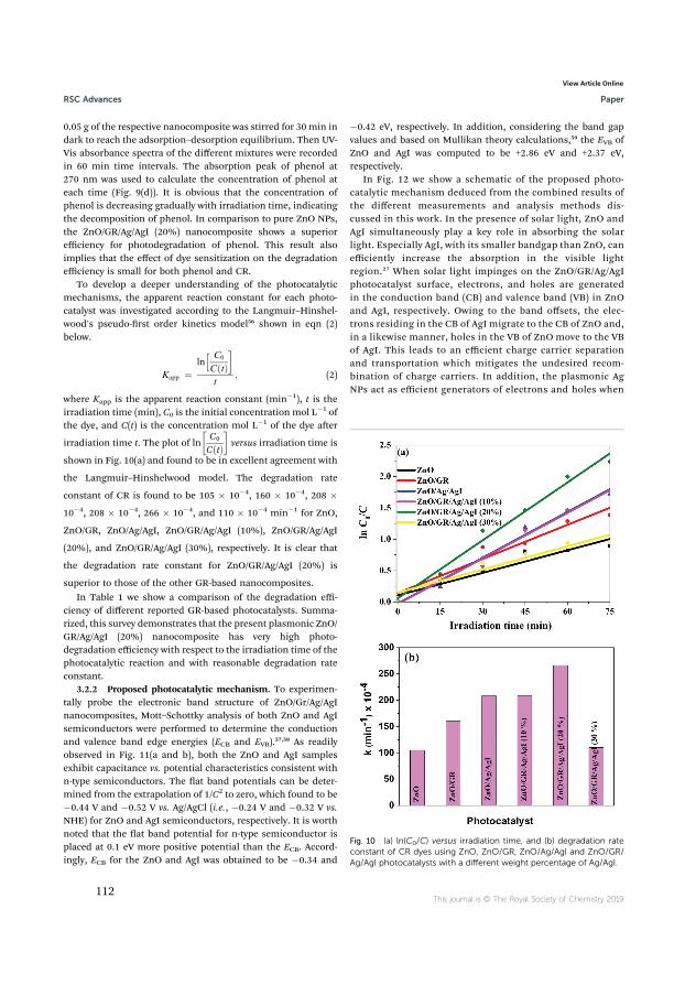
0.05 g of the respective nanocomposite was stirred for 30 min indark to reach the adsorption–desorption equilibrium. Then UV-Vis absorbance spectra of the different mixtures were recordedin 60 min time intervals. The absorption peak of phenol at270 nm was used to calculate the concentration of phenol ateach time (Fig. 9(d)). It is obvious that the concentration ofphenol is decreasing gradually with irradiation time, indicatingthe decomposition of phenol. In comparison to pure ZnO NPs,the ZnO/GR/Ag/AgI (20%) nanocomposite shows a superiorefficiency for photodegradation of phenol. This result alsoimplies that the effect of dye sensitization on the degradationefficiency is small for both phenol and CR.
To develop a deeper understanding of the photocatalyticmechanisms, the apparent reaction constant for each photo-catalyst was investigated according to the Langmuir–Hinshel-wood's pseudo-rst order kinetics model56 shown in eqn (2)below.
Kapp ¼lnh C0
CðtÞ�
t; (2)
where Kapp is the apparent reaction constant (min�1), t is theirradiation time (min), C0 is the initial concentration mol L�1 ofthe dye, and C(t) is the concentration mol L�1 of the dye aer
irradiation time t. The plot of ln�C0
CðtÞ�versus irradiation time is
shown in Fig. 10(a) and found to be in excellent agreement with
the Langmuir–Hinshelwood model. The degradation rate
constant of CR is found to be 105 � 10�4, 160 � 10�4, 208 �10�4, 208 � 10�4, 266 � 10�4, and 110 � 10�4 min�1 for ZnO,
ZnO/GR, ZnO/Ag/AgI, ZnO/GR/Ag/AgI (10%), ZnO/GR/Ag/AgI
(20%), and ZnO/GR/Ag/AgI (30%), respectively. It is clear that
the degradation rate constant for ZnO/GR/Ag/AgI (20%) is
superior to those of the other GR-based nanocomposites.In Table 1 we show a comparison of the degradation effi-
ciency of different reported GR-based photocatalysts. Summa-rized, this survey demonstrates that the present plasmonic ZnO/GR/Ag/AgI (20%) nanocomposite has very high photo-degradation efficiency with respect to the irradiation time of thephotocatalytic reaction and with reasonable degradation rateconstant.
3.2.2 Proposed photocatalytic mechanism. To experimen-tally probe the electronic band structure of ZnO/Gr/Ag/AgInanocomposites, Mott–Schottky analysis of both ZnO and AgIsemiconductors were performed to determine the conductionand valence band edge energies (ECB and EVB).57,58 As readilyobserved in Fig. 11(a and b), both the ZnO and AgI samplesexhibit capacitance vs. potential characteristics consistent withn-type semiconductors. The at band potentials can be deter-mined from the extrapolation of 1/C2 to zero, which found to be�0.44 V and �0.52 V vs. Ag/AgCl (i.e., �0.24 V and �0.32 V vs.NHE) for ZnO and AgI semiconductors, respectively. It is worthnoted that the at band potential for n-type semiconductor isplaced at 0.1 eV more positive potential than the ECB. Accord-ingly, ECB for the ZnO and AgI was obtained to be �0.34 and
�0.42 eV, respectively. In addition, considering the band gapvalues and based on Mullikan theory calculations,59 the EVB ofZnO and AgI was computed to be +2.86 eV and +2.37 eV,respectively.
In Fig. 12 we show a schematic of the proposed photo-catalytic mechanism deduced from the combined results ofthe different measurements and analysis methods dis-cussed in this work. In the presence of solar light, ZnO andAgI simultaneously play a key role in absorbing the solarlight. Especially AgI, with its smaller bandgap than ZnO, canefficiently increase the absorption in the visible lightregion.27 When solar light impinges on the ZnO/GR/Ag/AgIphotocatalyst surface, electrons, and holes are generatedin the conduction band (CB) and valence band (VB) in ZnOand AgI, respectively. Owing to the band offsets, the elec-trons residing in the CB of AgI migrate to the CB of ZnO and,in a likewise manner, holes in the VB of ZnO move to the VBof AgI. This leads to an efficient charge carrier separationand transportation which mitigates the undesired recom-bination of charge carriers. In addition, the plasmonic AgNPs act as efficient generators of electrons and holes when
Fig. 10 (a) ln(C0/C) versus irradiation time, and (b) degradation rateconstant of CR dyes using ZnO, ZnO/GR, ZnO/Ag/AgI and ZnO/GR/Ag/AgI photocatalysts with a different weight percentage of Ag/AgI.
This journal is © The Royal Society of Chemistry 2019
RSC Advances Paper
View Article Online
112
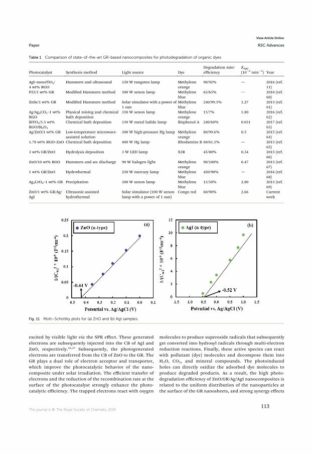
excited by visible light via the SPR effect. These generatedelectrons are subsequently injected into the CB of AgI andZnO, respectively.15,37 Subsequently, the photogeneratedelectrons are transferred from the CB of ZnO to the GR. TheGR plays a dual role of electron acceptor and transporter,which improve the photocatalytic behavior of the nano-composite under solar irradiation. The efficient transfer ofelectrons and the reduction of the recombination rate at thesurface of the photocatalyst strongly enhance the photo-catalytic efficiency. The trapped electrons react with oxygen
molecules to produce superoxide radicals that subsequentlyget converted into hydroxyl radicals through multi-electronreduction reactions. Finally, these active species can reactwith pollutant (dye) molecules and decompose them intoH2O, CO2, and mineral compounds. The photoinducedholes can directly oxidize the adsorbed dye molecules toproduce degraded products. As a result, the high photo-degradation efficiency of ZnO/GR/Ag/AgI nanocomposites isrelated to the uniform distribution of the nanoparticles atthe surface of the GR nanosheets, and strong synergy effects
Table 1 Comparison of state-of-the-art GR-based nanocomposites for photodegradation of organic dyes
Photocatalyst Synthesis method Light source DyeDegradation min/efficiency
Kapp
(10�2 min�1) Year
AgI–mesoTiO2/4 wt% RGO
Hummers and ultrasound 150 W tungsten lamp Methyleneorange
90/92% — 2016 (ref.11)
P25/1 wt% GR Modied Hummers method 500 W xenon lamp Methyleneblue
65/65% — 2010 (ref.60)
ZnSe/1 wt% GR Modied Hummers method Solar simulator with a power of1 sun
Methyleneblue
240/99.5% 1.27 2015 (ref.61)
Ag/Ag2CO3–1 wt%RGO
Physical mixing and chemicalbath deposition
350 W xenon lamp Methyleneorange
15/7% 1.80 2016 (ref.62)
BiVO4/5.5 wt%RGO/Bi2O3
Chemical bath deposition 150 W metal halide lamp Bisphenol A 240/60% 0.031 2017 (ref.63)
Ag/ZnO/1 wt% GR Low-temperature microwave-assisted solution
300 W high-pressure Hg lamp Methyleneorange
80/99.6% 0.5 2015 (ref.64)
1.78 wt% RGO–ZnO Chemical bath deposition 400 W Hg lamp Rhodamine B 60/61.5% — 2015 (ref.65)
3 wt% GR/ZnO Hydrolysis deposition 3 W LED lamp X3B 45/80% 0.34 2015 (ref.66)
ZnO/10 wt% RGO Hummers and arc discharge 90 W halogen light Methyleneorange
90/100% 0.47 2015 (ref.67)
1 wt% GR/ZnO Hydrothermal 250 W mercury lamp Methyleneblue
450/90% — 2016 (ref.68)
Ag2CrO4–1 wt% GR Precipitation 300 W xenon lamp Methyleneblue
15/50% 2.80 2015 (ref.69)
ZnO/1 wt% GR/Ag/AgI
Ultrasonic-assistedhydrothermal
Solar simulator (100 W xenonlamp with a power of 1 sun)
Congo red 60/90% 2.66 Currentwork
Fig. 11 Mott–Schottky plots for (a) ZnO and (b) AgI samples.
This journal is © The Royal Society of Chemistry 2019
Paper RSC Advances
View Article Online
113
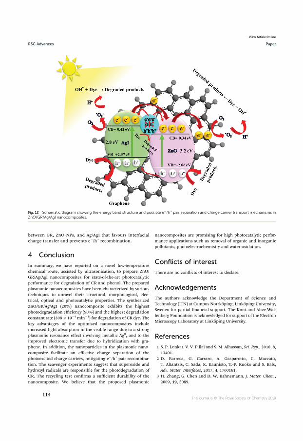
between GR, ZnO NPs, and Ag/AgI that favours interfacialcharge transfer and prevents e�/h+ recombination.
4 Conclusion
In summary, we have reported on a novel low-temperaturechemical route, assisted by ultrasonication, to prepare ZnO/GR/Ag/AgI nanocomposites for state-of-the-art photocatalyticperformance for degradation of CR and phenol. The preparedplasmonic nanocomposites have been characterized by varioustechniques to unravel their structural, morphological, elec-trical, optical and photocatalytic properties. The synthesizedZnO/GR/Ag/AgI (20%) nanocomposite exhibits the highestphotodegradation efficiency (90%) and the highest degradationconstant rate (308� 10�4 min�1) for degradation of CR dye. Thekey advantages of the optimized nanocomposites includeincreased light absorption in the visible range due to a strongplasmonic resonance effect involving metallic Ag0, and to theimproved electronic transfer due to hybridization with gra-phene. In addition, the nanoparticles in the plasmonic nano-composite facilitate an effective charge separation of thephotoexcited charge carriers, mitigating e�/h+ pair recombina-tion. The scavenger experiments suggest that superoxide andhydroxyl radicals are responsible for the photodegradation ofCR. The recycling test conrms a sufficient durability of thenanocomposite. We believe that the proposed plasmonic
nanocomposites are promising for high photocatalytic perfor-mance applications such as removal of organic and inorganicpollutants, photoelectrochemistry and water oxidation.
Conflicts of interest
There are no conicts of interest to declare.
Acknowledgements
The authors acknowledge the Department of Science andTechnology (ITN) at Campus Norrkoping, Linkoping University,Sweden for partial nancial support. The Knut and Alice Wal-lenberg Foundation is acknowledged for support of the ElectronMicroscopy Laboratory at Linkoping University.
References
1 S. P. Lonkar, V. V. Pillai and S. M. Alhassan, Sci. Rep., 2018, 8,13401.
2 D. Barreca, G. Carraro, A. Gasparotto, C. Maccato,T. Altantzis, C. Sada, K. Kaunisto, T.-P. Ruoko and S. Bals,Adv. Mater. Interfaces, 2017, 4, 1700161.
3 H. Zhang, G. Chen and D. W. Bahnemann, J. Mater. Chem.,2009, 19, 5089.
Fig. 12 Schematic diagram showing the energy band structure and possible e�/h+ pair separation and charge carrier transport mechanisms inZnO/GR/Ag/AgI nanocomposites.
This journal is © The Royal Society of Chemistry 2019
RSC Advances Paper
View Article Online
114
4 H. Wang, X. Liu and S. Han, CrystEngComm, 2016, 18, 1933–1943.
5 S. Kumar, A. Kumar, A. Kumar, R. Balaji and V. Krishnan,ChemistrySelect, 2018, 3, 1919–1932.
6 A. Kumar, V. Sharma, S. Kumar, A. Kumar and V. Krishnan,Surf. Interfaces, 2018, 11, 98–106.
7 W. Zhong, S. Shen, S. Feng, Z. Lin, Z. Wang and B. Fang,CrystEngComm, 2018, 20, 7851–7856.
8 Y. Liu, S. Shen, J. Zhang, W. Zhong and X. Huang, Appl. Surf.Sci., 2019, 478, 762–769.
9 G. Liao, Y. Gong, L. Zhang, H. Gao, G.-J. Yang and B. Fang,Energy Environ. Sci., 2019, 12, 2080–2147.
10 J. Xu, Y. Cui, Y. Han, M. Hao and X. Zhang, RSC Adv., 2016, 6,96778–96784.
11 R. Vinoth, P. Karthik, C. Muthamizhchelvan, B. Neppolianand M. Ashokkumar, Phys. Chem. Chem. Phys., 2016, 18,5179–5191.
12 A. Kumar, K. L. Reddy, S. Kumar, A. Kumar, V. Sharma andV. Krishnan, ACS Appl. Mater. Interfaces, 2018, 10, 15565–15581.
13 H. Sun and S. Wang, Energy Fuels, 2014, 28, 22–36.14 S. Lee, D. A. Reddy and T. Kyu Kim, RSC Adv., 2016, 6, 37180–
37188.15 J. Choi, D. A. Reddy, M. J. Islam, R. Ma and T. K. Kim, J. Alloys
Compd., 2016, 688, 527–536.16 N. Zhang, Y. Zhang and Y.-J. Xu, Nanoscale, 2012, 4, 5792–
5813.17 Q. Xiang, J. Yu and M. Jaroniec, Chem. Soc. Rev., 2012, 41,
782–796.18 B. Li, T. Liu, Y. Wang and Z. Wang, J. Colloid Interface Sci.,
2012, 377, 114–121.19 B. Li and H. Cao, J. Mater. Chem., 2011, 21, 3346–3349.20 E. Chalangar, H. Machhadani, S.-H. Lim, K. F. Karlsson,
O. Nur, M. Willander and H. Pettersson, Nanotechnology,2018, 29, 415201.
21 Z. Tian, S. Bai, K. Cao and J. Li, Mater. Express, 2016, 6, 437–443.
22 S. Y. Sawant and M. Hwan Cho, RSC Adv., 2015, 5, 97788–97797.
23 K. L. Reddy, S. Kumar, A. Kumar and V. Krishnan, J. Hazard.Mater., 2019, 367, 694–705.
24 A. Kumar, K. Kumar and V. Krishnan,Mater. Lett., 2019, 245,45–48.
25 D. A. Reddy, S. Lee, J. Choi, S. Park, R. Ma, H. Yang andT. K. Kim, Appl. Surf. Sci., 2015, 341, 175–184.
26 G. Li, Y. Wang and L. Mao, RSC Adv., 2014, 4, 53649–53661.27 M. Pirhashemi and A. Habibi-Yangjeh, Ceram. Int., 2017, 43,
13447–13460.28 N. Guy and M. Ozacar, J. Photochem. Photobiol., A, 2019, 370,
1–11.29 G. Liao, J. Fang, Q. Li, S. Li, Z. Xu and B. Fang, Nanoscale,
2019, 11, 7062–7096.30 W. Jiang, C. An, J. Liu, S. Wang, L. Zhao, W. Guo and J. Liu,
Dalton Trans., 2013, 43, 300–305.31 J. Yang, X. Zhao, X. Shan, H. Fan, L. Yang, Y. Zhang and X. Li,
J. Alloys Compd., 2013, 556, 1–5.
32 M. Pirhashemi and A. Habibi-Yangjeh, J. Colloid InterfaceSci., 2017, 491, 216–229.
33 B. Saravanakumar, R. Mohan and S.-J. Kim,Mater. Res. Bull.,2013, 48, 878–883.
34 D. Fu, G. Han, Y. Chang and J. Dong, Mater. Chem. Phys.,2012, 132, 673–681.
35 A. Monshi, M. R. Foroughi and M. R. Monshi, World J. NanoSci. Eng., 2012, 02, 154–160.
36 B. Qiu, Y. Zhou, Y. Ma, X. Yang, W. Sheng, M. Xing andJ. Zhang, Sci. Rep., 2015, 5, 8591.
37 S. Lu, H. Wang, J. Zhou, X. Wu and W. Qin, Nanoscale, 2017,9, 1184–1192.
38 V. Etacheri, R. Roshan and V. Kumar, ACS Appl. Mater.Interfaces, 2012, 4, 2717–2725.
39 H. Alnoor, G. Pozina, V. Khranovskyy, X. Liu, D. Iandolo,M. Willander and O. Nur, J. Appl. Phys., 2016, 119, 165702.
40 D. K. Mishra, J. Mohapatra, M. K. Sharma, R. Chattarjee,S. K. Singh, S. Varma, S. N. Behera, S. K. Nayak andP. Entel, J. Magn. Magn. Mater., 2013, 329, 146–152.
41 H. Moussa, E. Girot, K. Mozet, H. Alem, G. Medjahdi andR. Schneider, Appl. Catal., B, 2016, 185, 11–21.
42 A. Kumar, L. Rout, L. S. K. Achary, S. Keshari Mohanty andP. Dash, New J. Chem., 2017, 41, 10568–10583.
43 K. Dai, J. Lv, L. Lu, C. Liang, L. Geng and G. Zhu, Mater.Chem. Phys., 2016, 177, 529–537.
44 H. N. Tien, V. H. Luan, L. T. Hoa, N. T. Khoa, S. H. Hahn,J. S. Chung, E. W. Shin and S. H. Hur, Chem. Eng. J., 2013,229, 126–133.
45 C. Hu, T. Peng, X. Hu, Y. Nie, X. Zhou, J. Qu and H. He, J. Am.Chem. Soc., 2010, 132, 857–862.
46 M. R. Phillips, O. Gelhausen and E. M. Goldys, Phys. StatusSolidi A, 2004, 201, 229–234.
47 S. Choi, M. R. Phillips, I. Aharonovich, S. Pornsuwan,B. C. C. Cowie and C. Ton-That, Adv. Opt. Mater., 2015, 3,821–827.
48 V. Khranovskyy, V. Lazorenko, G. Lashkarev andR. Yakimova, J. Lumin., 2012, 132, 2643–2647.
49 B. Neppolian, A. Bruno, C. L. Bianchi and M. Ashokkumar,Ultrason. Sonochem., 2012, 19, 9–15.
50 J. Choi, D. A. Reddy and T. K. Kim, Ceram. Int., 2015, 41,13793–13803.
51 D. Amaranatha Reddy, R. Ma, M. Y. Choi and T. K. Kim, Appl.Surf. Sci., 2015, 324, 725–735.
52 T. T. H. Tran, H. Kosslick, A. Schulz and Q. L. Nguyen, Adv.Nat. Sci.: Nanosci. Nanotechnol., 2017, 8, 015011.
53 L. Hou, H. Zhang and X. Xue, Sep. Purif. Technol., 2012, 84,147–152.
54 A. L. Teel and R. J. Watts, J. Hazard. Mater., 2002, 94, 179–189.
55 D. Amaranatha Reddy, J. Choi, S. Lee, R. Ma and T. Kyu Kim,RSC Adv., 2015, 5, 67394–67404.
56 Y. Li, X. Li, J. Li and J. Yin, Water Res., 2006, 40, 1119–1126.57 N. Sedaghati, A. Habibi-Yangjeh, M. Pirhashemi and
S. Vadivel, J. Photochem. Photobiol., A, 2019, 384, 112066.58 S. Feizpoor, A. Habibi-Yangjeh, I. Ahadzadeh and K. Yubuta,
Adv. Powder Technol., 2019, 30, 1183–1196.59 A. H. Nethercot, Phys. Rev. Lett., 1974, 33, 1088–1091.
This journal is © The Royal Society of Chemistry 2019
Paper RSC Advances
View Article Online
115

60 H. Zhang, X. Lv, Y. Li, Y. Wang and J. Li, ACS Nano, 2010, 4,380–386.
61 S. H. Hsieh, W. J. Chen and T. H. Yeh, Appl. Surf. Sci., 2015,358, 63–69.
62 S. Song, B. Cheng, N. Wu, A. Meng, S. Cao and J. Yu, Appl.Catal., B, 2016, 181, 71–78.
63 P. Qiu, B. Park, J. Choi, M. Cui, J. Kim and J. Khim, J. AlloysCompd., 2017, 706, 7–15.
64 P. Dou, F. Tan, W. Wang, A. Sarreshteh, X. Qiao, X. Qiu andJ. Chen, J. Photochem. Photobiol., A, 2015, 302, 17–22.
65 T. N. Reddy, J. Manna and R. K. Rana, ACS Appl. Mater.Interfaces, 2015, 35, 19684–19690.
66 X. Wu, L. Wen, K. Lv, K. Deng, D. Tang, H. Ye, D. Du, S. Liuand M. Li, Appl. Surf. Sci., 2015, 358, 130–136.
67 A. A. Ashkarran and B. Mohammadi, Appl. Surf. Sci., 2015,342, 112–119.
68 E. Rokhsat and O. Akhavan, Appl. Surf. Sci., 2016, 371, 590–595.
69 D. Xu, B. Cheng, S. Cao and J. Yu, Appl. Catal., B, 2015, 164,380–388.
This journal is © The Royal Society of Chemistry 2019
RSC Advances Paper
View Article Online
116

III PAPER
117

118
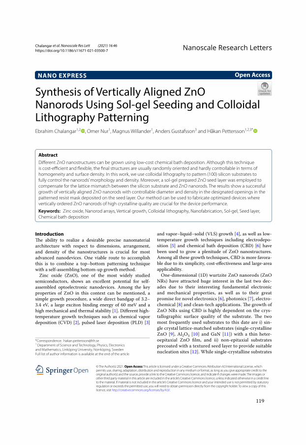
Chalangar et al. Nanoscale Res Lett (2021) 16:46 https://doi.org/10.1186/s11671-021-03500-7
NANO EXPRESS
Synthesis of Vertically Aligned ZnO Nanorods Using Sol-gel Seeding and Colloidal Lithography PatterningEbrahim Chalangar1,2 , Omer Nur1, Magnus Willander1, Anders Gustafsson3 and Håkan Pettersson1,2,3*
Abstract
Different ZnO nanostructures can be grown using low-cost chemical bath deposition. Although this technique is cost-efficient and flexible, the final structures are usually randomly oriented and hardly controllable in terms of homogeneity and surface density. In this work, we use colloidal lithography to pattern (100) silicon substrates to fully control the nanorods’ morphology and density. Moreover, a sol-gel prepared ZnO seed layer was employed to compensate for the lattice mismatch between the silicon substrate and ZnO nanorods. The results show a successful growth of vertically aligned ZnO nanorods with controllable diameter and density in the designated openings in the patterned resist mask deposited on the seed layer. Our method can be used to fabricate optimized devices where vertically ordered ZnO nanorods of high crystalline quality are crucial for the device performance.
Keywords: Zinc oxide, Nanorod arrays, Vertical growth, Colloidal lithography, Nanofabrication, Sol-gel, Seed layer, Chemical bath deposition
© The Author(s) 2021. Open Access This article is licensed under a Creative Commons Attribution 4.0 International License, which permits use, sharing, adaptation, distribution and reproduction in any medium or format, as long as you give appropriate credit to the original author(s) and the source, provide a link to the Creative Commons licence, and indicate if changes were made. The images or other third party material in this article are included in the article’s Creative Commons licence, unless indicated otherwise in a credit line to the material. If material is not included in the article’s Creative Commons licence and your intended use is not permitted by statutory regulation or exceeds the permitted use, you will need to obtain permission directly from the copyright holder. To view a copy of this licence, visit http://creat iveco mmons .org/licen ses/by/4.0/.
Introduction�e ability to realize a desirable precise nanomaterial architecture with respect to dimensions, arrangement, and density of the nanostructures is crucial for most advanced nanodevices. One viable route to accomplish this is to combine a top–bottom patterning technique with a self-assembling bottom-up growth method.
Zinc oxide (ZnO), one of the most widely studied semiconductors, shows an excellent potential for self-assembled optoelectronic nanodevices. Among the key properties of ZnO in this context can be mentioned, a simple growth procedure, a wide direct bandgap of 3.2–3.4 eV, a large exciton binding energy of 60 meV and a high mechanical and thermal stability [1]. Different high-temperature growth techniques such as chemical vapor deposition (CVD) [2], pulsed laser deposition (PLD) [3]
and vapor–liquid–solid (VLS) growth [4], as well as low-temperature growth techniques including electrodepo-sition [5] and chemical bath deposition (CBD) [6] have been used to grow a plenitude of ZnO nanostructures. Among all these growth techniques, CBD is more favora-ble due to its simplicity, cost-effectiveness and large-area applicability.
One-dimensional (1D) wurtzite ZnO nanorods (ZnO NRs) have attracted huge interest in the last two dec-ades due to their interesting fundamental electronic and mechanical properties, as well as to their great promise for novel electronics [6], photonics [7], electro-chemical [8] and clean-tech applications. �e growth of ZnO NRs using CBD is highly dependent on the crys-tallographic surface quality of the substrate. �e two most frequently used substrates to this date are i) sin-gle crystal lattice-matched substrates (single-crystalline ZnO [9], Al2O3 [10] and GaN [11]) with a thin heter-oepitaxial ZnO film, and ii) non-epitaxial substrates precoated with a textured seed layer to provide suitable nucleation sites [12]. While single-crystalline substrates
Open Access
*Correspondence: [email protected] Department of Science and Technology, Physics, Electronics and Mathematics, Linköping University, Norrköping, SwedenFull list of author information is available at the end of the article
119
Page 2 of 9Chalangar et al. Nanoscale Res Lett (2021) 16:46
generally result in significantly higher NR growth qual-ity, the high substrate cost limits their application. Con-versely, the growth of NRs on low-cost non-epitaxial substrates, supplied with a textured polycrystalline seed layer, leads to a randomly oriented NR growth.
In many high-performance device applications, a precise engineering of the NR surface density, lateral ordering, and vertical alignment is of great importance. Growth of NRs by CBD offers several straightforward ways to engineer the NR architecture on the substrate by controlling growth parameters such as solution concen-tration [13], temperature [14], pH [15], and deposition duration. Unfortunately, changing any of these growth parameters typically also causes undesired changes in the NR growth result. For this reason, up to now, sub-strate patterning is the most effective way to control the position, density and alignment of ZnO NRs. In the vast majority of reported studies, patterning of the substrate includes the following steps: substrate preparation and cleaning, deposition of a mask resist layer, opening holes in the resist layer by lithography for selective area growth, and CBD growth of NRs in the holes.
During the past decade, various efforts have been made to grow ordered vertical ZnO NR arrays. In the major-ity of these studies, using the same CBD technique, the authors have focused on two key processing steps: prep-aration of appropriate substrates, and usage of different patterning techniques, e.g., electron-beam lithography (EBL), laser interference lithography (LIL), and nano-imprint lithography (NIL). Wang et al. demonstrated non-epitaxial growth of vertically aligned ZnO NRs on EBL-patterned polycrystalline ZnO-coated Si and GaN substrates [11]. Later, they reported on perfectly aligned heteroepitaxial ZnO NR growth on GaN substrates pat-terned by LIL [16]. In an effort to replace the expensive ZnO and GaN substrates with low-cost Si or glass sub-strates, they successfully used a 30-µm-thick textured ZnO layer as a flat (0001) ZnO seed layer. In a series of articles, Volk et al. successfully performed homoepitaxial growth of ZnO NRs on single-crystalline ZnO substrates patterned by EBL [10, 17–19]. �e impact of differ-ent patterned substrates [10], a Zn-terminated versus O-terminated surface of the ZnO substrate [17], a sput-tered polycrystalline ZnO thin film [18], and a ZnO seedlayer deposited by atomic layer deposition (ALD) [19] onthe quality of CBD-grown ZnO NRs have been deeplyinvestigated. In a different approach, PLD was used forheteroepitaxial growth of a ZnO seed layer on a single-crystalline Al2O3 (0001) substrate, followed by NIL pat-terning [20]. More details about the Zn concentrationwindow in CBD and its effect on the ZnO NR morphol-ogy were discussed in the same article. Selective areagrowth of ZnO NRs on different substrates, including Si
(111), GaAs (111) and InP (111), using EBL patterning and electrochemical deposition has also been reported [21].
In all the reviewed references, the growth of ZnO NRs on a single-crystalline ZnO substrate results in the high-est crystal quality, while a coating with a thin polycrys-talline ZnO layer on other expensive single-crystalline substrates leads to excellent vertically aligned ZnO NR growth. Employing sophisticated patterning tech-niques, e.g., EBL, for selective growth of ZnO NRs also has an essential impact on the final product cost and, consequently, on the potential application. To overcome demanding complexity issues related to pattern defini-tion and expensive substrates in the fabrication of verti-cally aligned ZnO NR arrays, we propose to combine a simply prepared, highly uniform thin ZnO NP film on Si substrates with colloidal lithography (CL) patterning.
A sol-gel technique, described in [22], can be used to prepare a highly uniform, dense and thin seed layer of polycrystalline ZnO NPs on virtually any substrate, including Si or glass. In contrast to the spin-coating of a ZnO NP dispersion on a substrate, which usually leads to non-continuous dispersed islands of NP clusters [23], the sol-gel method results in a thin (tens of nm) continu-ous and highly uniform layer of ZnO NPs. For selective area CBD growth, a polymer resist layer is subsequently spin-coated on the ZnO seed layer and patterned by CL. Besides being a low-cost lithography method, CL isalso suitable for large wafer-scale area patterning, highthroughput, and compatibility with any substrate, offer-ing excellent control over feature size and pitch [24–26].
Figure 1 shows a schematic of the processing and growth steps used in the present work. After dip-coating the Si substrate with a ZnO NP seed layer and spin-coat-ing with a resist, respectively, a monolayer of polysty-rene nanobeads (PS-NBs) with a diameter of 140 nm was deposited on the resist mask and covered by a thermally evaporated 30 nm thick Al film. After evaporation, the Al-coated PS-NBs were removed by tape stripping, leaving behind open nanoholes in the Al film. Dry etch-ing of the resist in the holes down to the ZnO NP seed layer finalized the preparation of the growth mask. After CL, CBD was used to grow vertically aligned ZnO NRs with well-controlled diameter, length and surface den-sity. While CL and CBD have previously been deployed to grow ZnO NRs on micrometer-sized areas on ITO glass substrates, resulting in large uncontrolled batches of grown NRs [27], the present study is, to the best of our knowledge, the first demonstrated selective growth of single vertically aligned ZnO NRs in CL-patterned masks on sol-gel prepared Si substrates. �e results show a uni-form distribution of nanoholes on a large wafer-scale area
120
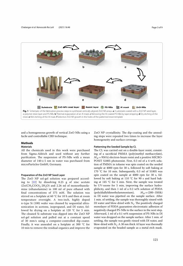
Page 3 of 9Chalangar et al. Nanoscale Res Lett (2021) 16:46
and a homogeneous growth of vertical ZnO NRs using a facile and controllable CBD technique.
MethodsMaterialsAll the chemicals used in this work were purchased from Sigma-Aldrich and used without any further purification. �e suspension of PS-NBs with a mean diameter of 140 ± 5 nm in water was purchased from microParticles GmbH, Germany.
Preparation of the ZnO NP Seed Layer�e ZnO NP sol-gel solution was prepared accord-ing to [22] by dissolving 8.25 g of zinc acetate (Zn(CH3COO)2·2H2O) and 2.26 ml of monoethanola-mine (ethanolamine) in 100 ml of pure ethanol with final concentrations of 375 mM. �e solution was stirred on a hotplate at 60 °C for 10 h and then at room temperature overnight. A two-inch, highly doped n-type Si (100) wafer was cleaned by sequential ultra-sonication in acetone, isopropanol, and DI water, fol-lowed by drying on a hotplate at 120 °C for 5 min. �e cleaned Si substrate was dipped into the ZnO NP sol-gel solution and pulled out at a constant speed of 30 mm/s using a computer-controlled dip-coater. Finally, it was annealed on a hotplate at 300 °C for 10 min to remove the residual organics and improve the
ZnO NP crystallinity. �e dip-coating and the anneal-ing steps were repeated two times to increase the layer homogeneity and surface coverage.
Patterning the Seeded Sample by CL�e CL was carried out on a double-layer resist, consist-ing of a sacrificial PMMA (poly(methyl methacrylate), MW = 950 k) electron-beam resist and a positive MICRO-POSIT S1805 photoresist. First, 0.3 ml of a 4 wt% solu-tion of PMMA in toluene was spin coated on the seeded sample at 4000 rpm for 30 s, followed by soft baking at 170 °C for 10 min. Subsequently, 0.3 ml of S1805 was spin coated on the sample at 4000 rpm for 30 s, fol-lowed by soft baking at 110 °C for 90 s and hard bak-ing at 145 °C for 5 min. Next, the sample was treated by UV-ozone for 5 min, improving the surface hydro-philicity, and then 1 ml of a 0.2 wt% solution of PDDA (poly(diallyldimethylammonium), MW = (200–350)k) in DI water was pipetted on the sample surface. After 1 min. of settling, the sample was thoroughly rinsed with DI water and blow-dried with N2. �e positively charged monolayer of PDDA guarantees electrostatic adhesion of negatively charged PS-NBs to the surface in the next step. Afterward, 1 ml of a 0.1 wt% suspension of PS-NBs in DI water was dropped on the sample surface. After 1 min. of settling, the sample was gently rinsed with DI water, and blow-dried with N2. A 30 nm thick Al layer was thermally evaporated on the beaded sample as a metal etch mask.
Fig. 1 Schematic of the fabrication process steps to synthesize vertically aligned ZnO NR arrays. a A substrate coated with a ZnO NP seed layer, a polymer resist layer and PS-NBs. b Thermal evaporation of an Al mask. c Removing the Al-coated PS-NBs by tape stripping. d Dry etching of the resist. e Wet etching of the Al mask. f Selective ZnO NR growth in the holes of the patterned resist template
121
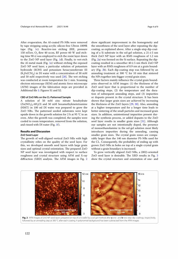
Page 4 of 9Chalangar et al. Nanoscale Res Lett (2021) 16:46
After evaporation, the Al-coated PS-NBs were removed by tape stripping using acrylic silicon-free Ultron 1009R tape (Fig. 1c). Reactive-ion etching (RIE, pressure 150 mTorr, O2 flow 40 sccm, RF power 60 W and etch-ing time 90 s) was employed to etch the resist layer down to the ZnO NP seed layer (Fig. 1d). Finally, to wet-etch the Al metal mask (Fig. 1e) without etching the exposed ZnO NP seed layer, a particular solution of potassium hydroxide (KOH) and potassium hexacyanoferrate III (K3Fe(CN)6) in DI water with a concentration of 30 mM and 50 mM respectively was used [28]. �e wet etching was conducted at room temperature for 1 min. Scanning electron microscopy (SEM) and atomic force microscopy (AFM) images of the fabrication steps are provided in Additional file 1: Figures S1 and S2.
CBD of ZnO NRs on the CL-Patterned SampleA solution of 50 mM zinc nitrate hexahydrate (Zn(NO3)2·6H2O) and 50 mM hexamethylenetetramine(HMT) in 100 ml DI water was prepared to grow the ZnO NRs. �e patterned seeded substrates were kept upside down in the growth solution for 2 h at 95 °C in an oven. After the growth was completed, the samples were cooled to room temperature, removed from the solution, and rinsed with DI water (Fig. 1f ).
Results and DiscussionZnO Seed Layer�e growth of well-aligned vertical ZnO NRs with high crystallinity relies on the quality of the seed layer. For this, we developed smooth seed layers with large grain sizes and optimal crystal orientation. �e prepared ZnO NP seed layer was investigated with respect to surface roughness and crystal structure using AFM and X-ray diffraction (XRD) analysis. �e AFM images in Fig. 2
show significant improvement in the homogeneity and the smoothness of the seed layer after repeating the dip-coating, as explained above. After a single-step dip-coat-ing of a Si substrate in the sol-gel solution, a 21 ± 5 nm thick ZnO NP layer with an RMS roughness of 1.2 nm (Fig. 2a) was formed on the Si surface. Repeating the dip-coating resulted in a smoother 40 ± 5 nm thick ZnO NPlayer with an RMS roughness of 0.9 nm at a grain bound-ary (Fig. 2b). Each dip-coating step was followed by an annealing treatment at 300 °C for 10 min that sintered the NPs together into bigger crystal grain sizes.
�ree factors mainly influence the crystal grain bound-aries observed in AFM images: (1) the thickness of the ZnO seed layer that is proportional to the number of dip-coating steps, (2) the temperature and the dura-tion of subsequent annealing steps, and (3) impurities or dopants present in the crystal structure. It has been shown that larger grain sizes are achieved by increasing the thickness of the ZnO layers [29, 30]. Also, annealing at a higher temperature and for a longer time leads to better sintering of the small particles and increased grain sizes. In addition, unintentional impurities present dur-ing the synthesis process, or added dopants to the ZnO seed layer results in smaller grain sizes [31]. Although our samples are not intentionally doped, the presence of monoethanolamine in the sol-gel solution most likely introduces impurities during the annealing, causing smaller grain sizes. �e crystal grain zones are compa-rably larger than the 140 nm diameter PS-NBs used for the CL. Consequently, the probability of ending up with grown ZnO NRs in holes on top of a single crystal grain without a grain boundary is increased.
To grow vertically aligned ZnO NRs, a (002)-oriented ZnO seed layer is desirable. �e XRD results in Fig. 3 show the crystal structure and orientation of one- and
Fig. 2 AFM images of ZnO NP seed layers prepared on top of a Si wafer by a sol-gel method after a one- and b two-step dip-coatings, respectively, followed by an annealing step at 300 °C after each coating. A polynomial background has been subtracted from the AFM images
122
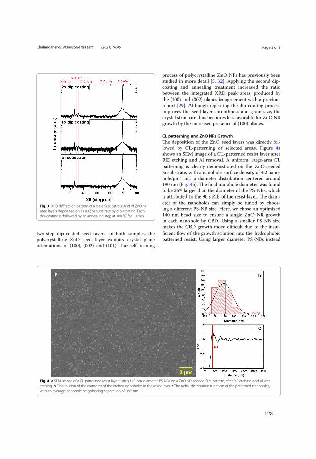
Page 5 of 9Chalangar et al. Nanoscale Res Lett (2021) 16:46
two-step dip-coated seed layers. In both samples, the polycrystalline ZnO seed layer exhibits crystal plane orientations of (100), (002) and (101). �e self-forming
process of polycrystalline ZnO NPs has previously been studied in more detail [5, 32]. Applying the second dip-coating and annealing treatment increased the ratio between the integrated XRD peak areas produced by the (100) and (002) planes in agreement with a previous report [29]. Although repeating the dip-coating process improves the seed layer smoothness and grain size, the crystal structure thus becomes less favorable for ZnO NR growth by the increased presence of (100) planes.
CL patterning and ZnO NRs Growth�e deposition of the ZnO seed layers was directly fol-lowed by CL-patterning of selected areas. Figure 4a shows an SEM image of a CL-patterned resist layer after RIE etching and Al removal. A uniform, large-area CL patterning is clearly demonstrated on the ZnO-seeded Si substrate, with a nanohole surface density of 4.2 nano-hole/µm2 and a diameter distribution centered around 190 nm (Fig. 4b). �e final nanohole diameter was found to be 36% larger than the diameter of the PS-NBs, which is attributed to the 90 s RIE of the resist layer. �e diam-eter of the nanoholes can simply be tuned by choos-ing a different PS-NB size. Here, we chose an optimized 140 nm bead size to ensure a single ZnO NR growth in each nanohole by CBD. Using a smaller PS-NB size makes the CBD growth more difficult due to the insuf-ficient flow of the growth solution into the hydrophobic patterned resist. Using larger diameter PS-NBs instead
Fig. 3 XRD diffraction pattern of a bare Si substrate and of ZnO NP seed layers deposited on a (100) Si substrate by dip-coating. Each dip-coating is followed by an annealing step at 300 °C for 10 min
Fig. 4 a SEM image of a CL-patterned resist layer using 140-nm-diameter PS-NBs on a ZnO NP-seeded Si substrate, after RIE etching and Al wet etching. b Distribution of the diameter of the etched nanoholes in the resist layer. c The radial distribution function of the patterned nanoholes, with an average nanohole neighboring separation of 392 nm
123
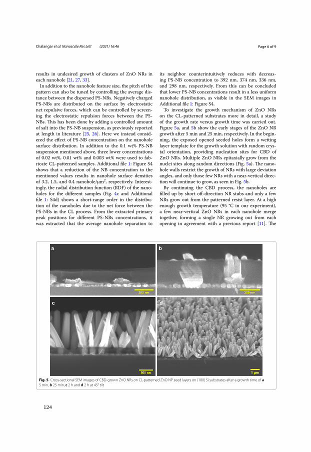
Page 6 of 9Chalangar et al. Nanoscale Res Lett (2021) 16:46
results in undesired growth of clusters of ZnO NRs in each nanohole [21, 27, 33].
In addition to the nanohole feature size, the pitch of the pattern can also be tuned by controlling the average dis-tance between the dispersed PS-NBs. Negatively charged PS-NBs are distributed on the surface by electrostatic net repulsive forces, which can be controlled by screen-ing the electrostatic repulsion forces between the PS-NBs. �is has been done by adding a controlled amount of salt into the PS-NB suspension, as previously reported at length in literature [25, 26]. Here we instead consid-ered the effect of PS-NB concentration on the nanohole surface distribution. In addition to the 0.1 wt% PS-NB suspension mentioned above, three lower concentrations of 0.02 wt%, 0.01 wt% and 0.003 wt% were used to fab-ricate CL-patterned samples. Additional file 1: Figure S4 shows that a reduction of the NB concentration to the mentioned values results in nanohole surface densities of 3.2, 1.5, and 0.4 nanohole/µm2, respectively. Interest-ingly, the radial distribution function (RDF) of the nano-holes for the different samples (Fig. 4c and Additional file 1: S4d) shows a short-range order in the distribu-tion of the nanoholes due to the net force between the PS-NBs in the CL process. From the extracted primary peak positions for different PS-NBs concentrations, it was extracted that the average nanohole separation to
its neighbor counterintuitively reduces with decreas-ing PS-NB concentration to 392 nm, 374 nm, 336 nm, and 298 nm, respectively. From this can be concluded that lower PS-NB concentrations result in a less uniform nanohole distribution, as visible in the SEM images in Additional file 1: Figure S4.
To investigate the growth mechanism of ZnO NRs on the CL-patterned substrates more in detail, a study of the growth rate versus growth time was carried out. Figure 5a, and 5b show the early stages of the ZnO NR growth after 5 min and 25 min, respectively. In the begin-ning, the exposed opened seeded holes form a wetting layer template for the growth solution with random crys-tal orientation, providing nucleation sites for CBD of ZnO NRs. Multiple ZnO NRs epitaxially grow from the nuclei sites along random directions (Fig. 5a). �e nano-hole walls restrict the growth of NRs with large deviation angles, and only those few NRs with a near-vertical direc-tion will continue to grow, as seen in Fig. 5b.
By continuing the CBD process, the nanoholes are filled up by short off-direction NR stubs and only a few NRs grow out from the patterned resist layer. At a high enough growth temperature (95 °C in our experiment), a few near-vertical ZnO NRs in each nanohole merge together, forming a single NR growing out from each opening in agreement with a previous report [11]. �e
Fig. 5 Cross-sectional SEM images of CBD-grown ZnO NRs on CL-patterned ZnO NP seed layers on (100) Si substrates after a growth time of a 5 min, b 25 min, c 2 h and d 2 h at 45° tilt
124
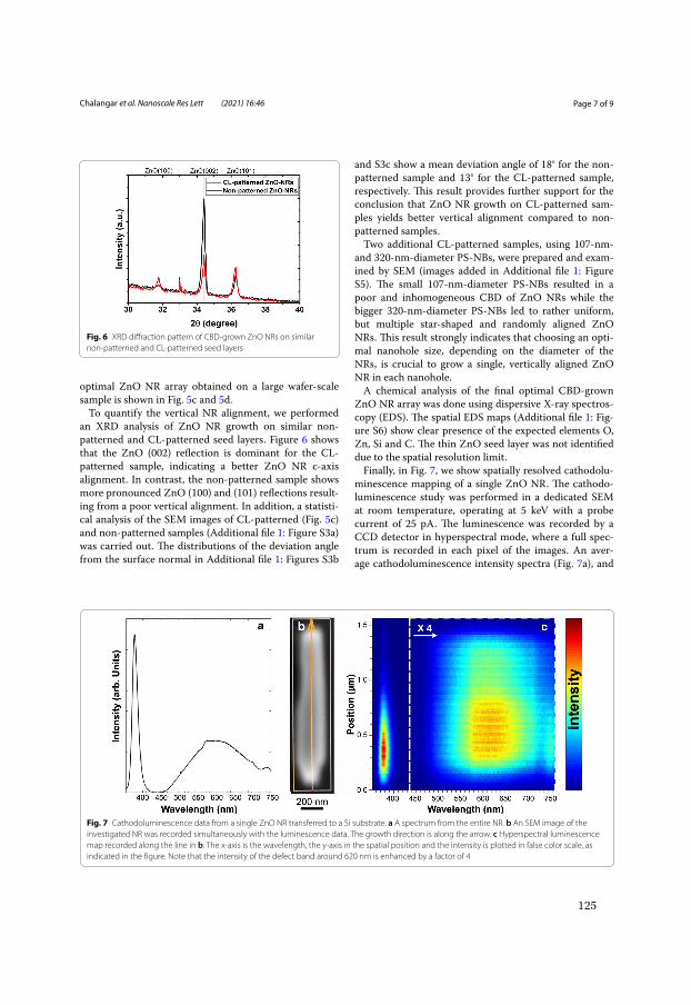
Page 7 of 9Chalangar et al. Nanoscale Res Lett (2021) 16:46
optimal ZnO NR array obtained on a large wafer-scale sample is shown in Fig. 5c and 5d.
To quantify the vertical NR alignment, we performed an XRD analysis of ZnO NR growth on similar non-patterned and CL-patterned seed layers. Figure 6 shows that the ZnO (002) reflection is dominant for the CL-patterned sample, indicating a better ZnO NR c-axis alignment. In contrast, the non-patterned sample shows more pronounced ZnO (100) and (101) reflections result-ing from a poor vertical alignment. In addition, a statisti-cal analysis of the SEM images of CL-patterned (Fig. 5c) and non-patterned samples (Additional file 1: Figure S3a) was carried out. �e distributions of the deviation angle from the surface normal in Additional file 1: Figures S3b
and S3c show a mean deviation angle of 18° for the non-patterned sample and 13° for the CL-patterned sample, respectively. �is result provides further support for the conclusion that ZnO NR growth on CL-patterned sam-ples yields better vertical alignment compared to non-patterned samples.
Two additional CL-patterned samples, using 107-nm- and 320-nm-diameter PS-NBs, were prepared and exam-ined by SEM (images added in Additional file 1: Figure S5). �e small 107-nm-diameter PS-NBs resulted in a poor and inhomogeneous CBD of ZnO NRs while the bigger 320-nm-diameter PS-NBs led to rather uniform, but multiple star-shaped and randomly aligned ZnO NRs. �is result strongly indicates that choosing an opti-mal nanohole size, depending on the diameter of the NRs, is crucial to grow a single, vertically aligned ZnO NR in each nanohole.
A chemical analysis of the final optimal CBD-grown ZnO NR array was done using dispersive X-ray spectros-copy (EDS). �e spatial EDS maps (Additional file 1: Fig-ure S6) show clear presence of the expected elements O, Zn, Si and C. �e thin ZnO seed layer was not identified due to the spatial resolution limit.
Finally, in Fig. 7, we show spatially resolved cathodolu-minescence mapping of a single ZnO NR. �e cathodo-luminescence study was performed in a dedicated SEM at room temperature, operating at 5 keV with a probe current of 25 pA. �e luminescence was recorded by a CCD detector in hyperspectral mode, where a full spec-trum is recorded in each pixel of the images. An aver-age cathodoluminescence intensity spectra (Fig. 7a), and
Fig. 6 XRD diffraction pattern of CBD-grown ZnO NRs on similar non-patterned and CL-patterned seed layers
Fig. 7 Cathodoluminescence data from a single ZnO NR transferred to a Si substrate. a A spectrum from the entire NR. b An SEM image of the investigated NR was recorded simultaneously with the luminescence data. The growth direction is along the arrow. c Hyperspectral luminescence map recorded along the line in b. The x-axis is the wavelength, the y-axis in the spatial position and the intensity is plotted in false color scale, as indicated in the figure. Note that the intensity of the defect band around 620 nm is enhanced by a factor of 4
125
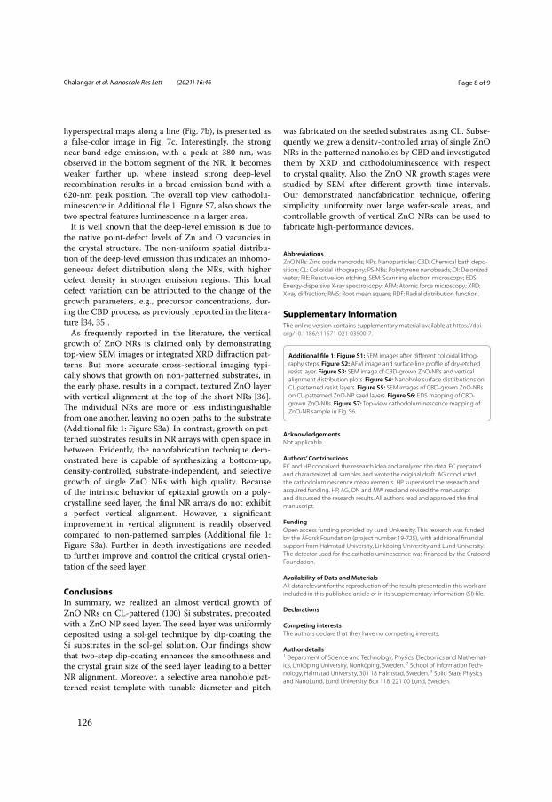
Page 8 of 9Chalangar et al. Nanoscale Res Lett (2021) 16:46
hyperspectral maps along a line (Fig. 7b), is presented as a false-color image in Fig. 7c. Interestingly, the strong near-band-edge emission, with a peak at 380 nm, was observed in the bottom segment of the NR. It becomes weaker further up, where instead strong deep-level recombination results in a broad emission band with a 620-nm peak position. �e overall top view cathodolu-minescence in Additional file 1: Figure S7, also shows thetwo spectral features luminescence in a larger area.
It is well known that the deep-level emission is due to the native point-defect levels of Zn and O vacancies in the crystal structure. �e non-uniform spatial distribu-tion of the deep-level emission thus indicates an inhomo-geneous defect distribution along the NRs, with higher defect density in stronger emission regions. �is local defect variation can be attributed to the change of the growth parameters, e.g., precursor concentrations, dur-ing the CBD process, as previously reported in the litera-ture [34, 35].
As frequently reported in the literature, the vertical growth of ZnO NRs is claimed only by demonstrating top-view SEM images or integrated XRD diffraction pat-terns. But more accurate cross-sectional imaging typi-cally shows that growth on non-patterned substrates, in the early phase, results in a compact, textured ZnO layer with vertical alignment at the top of the short NRs [36]. �e individual NRs are more or less indistinguishable from one another, leaving no open paths to the substrate (Additional file 1: Figure S3a). In contrast, growth on pat-terned substrates results in NR arrays with open space in between. Evidently, the nanofabrication technique dem-onstrated here is capable of synthesizing a bottom-up, density-controlled, substrate-independent, and selective growth of single ZnO NRs with high quality. Because of the intrinsic behavior of epitaxial growth on a poly-crystalline seed layer, the final NR arrays do not exhibit a perfect vertical alignment. However, a significant improvement in vertical alignment is readily observed compared to non-patterned samples (Additional file 1: Figure S3a). Further in-depth investigations are needed to further improve and control the critical crystal orien-tation of the seed layer.
ConclusionsIn summary, we realized an almost vertical growth of ZnO NRs on CL-pattered (100) Si substrates, precoated with a ZnO NP seed layer. �e seed layer was uniformly deposited using a sol-gel technique by dip-coating the Si substrates in the sol-gel solution. Our findings show that two-step dip-coating enhances the smoothness and the crystal grain size of the seed layer, leading to a better NR alignment. Moreover, a selective area nanohole pat-terned resist template with tunable diameter and pitch
was fabricated on the seeded substrates using CL. Subse-quently, we grew a density-controlled array of single ZnO NRs in the patterned nanoholes by CBD and investigated them by XRD and cathodoluminescence with respect to crystal quality. Also, the ZnO NR growth stages were studied by SEM after different growth time intervals. Our demonstrated nanofabrication technique, offering simplicity, uniformity over large wafer-scale areas, and controllable growth of vertical ZnO NRs can be used to fabricate high-performance devices.
AbbreviationsZnO NRs: Zinc oxide nanorods; NPs: Nanoparticles; CBD: Chemical bath depo-sition; CL: Colloidal lithography; PS-NBs: Polystyrene nanobeads; DI: Deionized water; RIE: Reactive-ion etching; SEM: Scanning electron microscopy; EDS: Energy-dispersive X-ray spectroscopy; AFM: Atomic force microscopy; XRD: X-ray diffraction; RMS: Root mean square; RDF: Radial distribution function.
Supplementary InformationThe online version contains supplementary material available at https ://doi.org/10.1186/s1167 1-021-03500 -7.
Additional le 1: Figure S1: SEM images after different colloidal lithog-raphy steps. Figure S2: AFM image and surface line profile of dry-etched resist layer. Figure S3: SEM image of CBD-grown ZnO-NRs and vertical alignment distribution plots. Figure S4: Nanohole surface distributions on CL-patterned resist layers. Figure S5: SEM images of CBD-grown ZnO-NRs on CL-patterned ZnO-NP seed layers. Figure S6: EDS mapping of CBD-grown ZnO-NRs. Figure S7: Top-view cathodoluminescence mapping of ZnO-NR sample in Fig. S6.
AcknowledgementsNot applicable.
Authors’ ContributionsEC and HP conceived the research idea and analyzed the data. EC prepared and characterized all samples and wrote the original draft. AG conducted the cathodoluminescence measurements. HP supervised the research and acquired funding. HP, AG, ON and MW read and revised the manuscript and discussed the research results. All authors read and approved the final manuscript.
FundingOpen access funding provided by Lund University. This research was funded by the ÅForsk Foundation (project number 19-725), with additional financial support from Halmstad University, Linköping University and Lund University. The detector used for the cathodoluminescence was financed by the Crafoord Foundation.
Availability of Data and MaterialsAll data relevant for the reproduction of the results presented in this work are included in this published article or in its supplementary information (SI) file.
Declarations
Competing interestsThe authors declare that they have no competing interests.
Author details1 Department of Science and Technology, Physics, Electronics and Mathemat-ics, Linköping University, Norrköping, Sweden. 2 School of Information Tech-nology, Halmstad University, 301 18 Halmstad, Sweden. 3 Solid State Physics and NanoLund, Lund University, Box 118, 221 00 Lund, Sweden.
126

Page 9 of 9Chalangar et al. Nanoscale Res Lett (2021) 16:46
Received: 20 November 2020 Accepted: 21 February 2021
References 1. Kołodziejczak-Radzimska A, Jesionowski T (2014) Zinc oxide—from
synthesis to application: a review. Materials 7:2833–2881. https ://doi.org/10.3390/ma704 2833
2. Müller R, Huber F, Gelme O et al (2019) Chemical vapor deposition growth of zinc oxide on sapphire with methane: initial crystal formation process. Cryst Growth Des 19:4964–4969. https ://doi.org/10.1021/acs.cgd.9b001 81
3. Rahman F (2019) Zinc oxide light-emitting diodes: a review. OE 58:010901. https ://doi.org/10.1117/1.OE.58.1.01090 1
4. Gomez JL, Tigli O (2013) Zinc oxide nanostructures: from growth to application. J Mater Sci 48:612–624. https ://doi.org/10.1007/s1085 3-012-6938-5
5. Skompska M, Zarębska K (2014) Electrodeposition of ZnO nanorod arrays on transparent conducting substrates—a review. Electrochim Acta 127:467–488. https ://doi.org/10.1016/j.elect acta.2014.02.049
6. Xu S, Wang ZL (2011) One-dimensional ZnO nanostructures: solution growth and functional properties. Nano Res 4:1013–1098. https ://doi.org/10.1007/s1227 4-011-0160-7
7. Cui J (2012) Zinc oxide nanowires. Mater Charact 64:43–52. https ://doi.org/10.1016/j.match ar.2011.11.017
8. Adam RE, Chalangar E, Pirhashemi M et al (2019) Graphene-based plas-monic nanocomposites for highly enhanced solar-driven photocatalytic activities. RSC Adv 9:30585–30598. https ://doi.org/10.1039/C9RA0 6273D
9. Consonni V, Sarigiannidou E, Appert E et al (2014) Selective area growth of well-ordered ZnO nanowire arrays with controllable polarity. ACS Nano 8:4761–4770. https ://doi.org/10.1021/nn500 620t
10. Erdélyi R, Nagata T, Rogers DJ et al (2011) Investigations into the impact of the template layer on ZnO nanowire arrays made using low tempera-ture wet chemical growth. Cryst Growth Des 11:2515–2519. https ://doi.org/10.1021/cg200 2755
11. Xu S, Wei Y, Kirkham M et al (2008) Patterned growth of vertically aligned ZnO nanowire arrays on inorganic substrates at low temperature without catalyst. J Am Chem Soc 130:14958–14959. https ://doi.org/10.1021/ja806 952j
12. Greene LE, Law M, Tan DH et al (2005) General route to vertical ZnO nanowire arrays using textured ZnO seeds. Nano Lett 5:1231–1236. https ://doi.org/10.1021/nl050 788p
13. Yilmaz C, Unal U (2016) Effect of Zn(NO3)2 concentration in hydrother-mal–electrochemical deposition on morphology and photoelectro-chemical properties of ZnO nanorods. Appl Surf Sci 368:456–463. https ://doi.org/10.1016/j.apsus c.2016.01.253
14. Amin G, Asif MH, Zainelabdin A et al (2011) Influence of pH, precursor concentration, growth time, and temperature on the morphology of ZnO nanostructures grown by the hydrothermal method. J Nanomater 2011:5:5. https ://doi.org/10.1155/2011/26969 2
15. Verrier C, Appert E, Chaix-Pluchery O et al (2017) Effects of the pH on the formation and doping mechanisms of ZnO nanowires using alu-minum nitrate and ammonia. Inorg Chem 56:13111–13122. https ://doi.org/10.1021/acs.inorg chem.7b019 16
16. Wei Y, Wu W, Guo R et al (2010) Wafer-scale high-throughput ordered growth of vertically aligned ZnO nanowire arrays. Nano Lett 10:3414–3419. https ://doi.org/10.1021/nl101 4298
17. Volk J, Nagata T, Erdélyi R et al (2009) Highly uniform epitaxial ZnO nanorod arrays for nanopiezotronics. Nanoscale Res Lett 4:699–704. https ://doi.org/10.1007/s1167 1-009-9302-1
18. Szabó Z, Volk J, Fülöp E et al (2013) Regular ZnO nanopillar arrays by nanosphere photolithography. Photonics Nanostruct Fundam Appl 11:1–7. https ://doi.org/10.1016/j.photo nics.2012.06.009
19. Szabó Z, Cora I, Horváth Z et al (2018) Hierarchical oxide nanostructures fabricated with atomic layer deposition and hydrothermal growth. Nano Struct Nano Objects 13:100–108. https ://doi.org/10.1016/j.nanos o.2017.12.006
20. Sakai D, Nagashima K, Yoshida H et al (2019) Substantial narrowing on the width of “concentration window” of hydrothermal ZnO nanowires via ammonia addition. Sci Rep 9:1–10. https ://doi.org/10.1038/s4159 8-019-50641 -y
21. Pham HT, Nguyen TD, Tran DQ, Akabori M (2017) Structural, optical and electrical properties of well-ordered ZnO nanowires grown on (1 1 1) ori-ented Si, GaAs and InP substrates by electrochemical deposition method. Mater Res Express 4:055002. https ://doi.org/10.1088/2053-1591/aa6c9 a
22. Parize R, Garnier JD, Appert E et al (2018) Effects of polyethylenimine and its molecular weight on the chemical bath deposition of ZnO nanowires. ACS Omega 3:12457–12464. https ://doi.org/10.1021/acsom ega.8b016 41
23. Alnoor H, Pozina G, Khranovskyy V et al (2016) Influence of ZnO seed layer precursor molar ratio on the density of interface defects in low temperature aqueous chemically synthesized ZnO nanorods/GaN light-emitting diodes. J Appl Phys 119:165702. https ://doi.org/10.1063/1.49475 93
24. Fredriksson H, Alaverdyan Y, Dmitriev A et al (2007) Hole-mask col-loidal lithography. Adv Mater 19:4297–4302. https ://doi.org/10.1002/adma.20070 0680
25. Hanarp P, Sutherland D, Gold J, Kasemo B (1999) Nanostructured model biomaterial surfaces prepared by colloidal lithography. Nanostruct Mater 12:429–432. https ://doi.org/10.1016/S0965 -9773(99)00151 -8
26. Cesaria M, Taurino A, Manera MG et al (2019) Gold nanoholes fabricated by colloidal lithography: novel insights into nanofabrication, short-range correlation and optical properties. Nanoscale 11:8416–8432. https ://doi.org/10.1039/C8NR0 9911A
27. Chen K, Thang DD, Ishii S et al (2015) Selective patterned growth of ZnO nanowires/nanosheets and their photoluminescence properties. Opt Mater Express: OME 5:353–360. https ://doi.org/10.1364/OME.5.00035 3
28. Vellekoop MJ, Visser CCO, Sarro PM, Venema A (1990) Compatibility of zinc oxide with silicon IC processing. Sens Actuators A 23:1027–1030. https ://doi.org/10.1016/0924-4247(90)87083 -U
29. Nian Q, Callahan M, Look D et al (2015) Highly transparent conduc-tive electrode with ultra-low HAZE by grain boundary modification of aqueous solution fabricated alumina-doped zinc oxide nanocrystals. APL Mater 3:062803. https ://doi.org/10.1063/1.49154 89
30. Kumar M, Kanjilal A, Som T (2013) Effect of grain-boundaries on electrical properties of n-ZnO:Al/p-Si heterojunction diodes. AIP Adv 3:092126. https ://doi.org/10.1063/1.48234 80
31. Bandyopadhyay S, Paul GK, Roy R et al (2002) Study of structural and electrical properties of grain-boundary modified ZnO films prepared by sol–gel technique. Mater Chem Phys 74:83–91. https ://doi.org/10.1016/S0254 -0584(01)00402 -3
32. Zhang Z, Meng G, Xu Q et al (2010) Aligned ZnO nanorods with tunable size and field emission on native si substrate achieved via simple electro-deposition. J Phys Chem C 114:189–193. https ://doi.org/10.1021/jp908 7223
33. Pea M, Maiolo L, Pilloton R et al (2014) ZnO nanowires strips growth: tem-plate reliability and morphology study. Microelectron Eng 121:147–152. https ://doi.org/10.1016/j.mee.2014.04.045
34. Watanabe K, Nagata T, Oh S et al (2016) Arbitrary cross-section SEM-cathodoluminescence imaging of growth sectors and local carrier concentrations within micro-sampled semiconductor nanorods. Nat Commun 7:10609. https ://doi.org/10.1038/ncomm s1060 9
35. Consonni V, Lord AM (2021) Polarity in ZnO nanowires: a critical issue for piezotronic and piezoelectric devices. Nano Energy 83:105789. https ://doi.org/10.1016/j.nanoe n.2021.10578 9
36. Zhou Q, Wen JZ, Zhao P, Anderson WA (2017) Synthesis of vertically-aligned zinc oxide nanowires and their application as a photocatalyst. Nanomaterials 7:9. https ://doi.org/10.3390/nano7 01000 9
Publisher’s NoteSpringer Nature remains neutral with regard to jurisdictional claims in pub-lished maps and institutional affiliations.
127

128
Paper IV
“Nanopatterned reduced graphene oxide/Al-doped ZnO seed layer for vertical growth of single ZnO nanorods on various substrates” has been removed for copyright reasons. For more details about these see: http://urn.kb.se/resolve?urn=urn:nbn:se:liu:diva-174835

Synthesis and Characterization of ZnO/Graphene Nanostructures for Electronics and Photocatalysis
Linköping Studies in Science and TechnologyDissertations No. 2130
Ebrahim Chalangar
Ebrahim Chalangar Synthesis and Characterization of ZnO/Graphene Nanostructures for Electronics and Photocatalysis 2021
FACULTY OF SCIENCE AND ENGINEERING
Linköping Studies in Science and Technology, Dissertation No. 2130Department of Science and Technology, 2021
Linköping UniversitySE-581 83 Linköping, Sweden
www.liu.se