Embed Size (px)
Citation preview
SYNTHESIS AND MECHANICAL PROPERTIES OF BULK QUANTITIES OF ELECTRODEPOSITED
NANOCRYSTALLINE MATERIALS
by
Iain Brooks
A thesis submitted in conformity with the requirements
for the degree of Doctor of Philosophy
Department of Materials Science and Engineering
University of Toronto
© Copyright by Iain Brooks (2012)
ii
Synthesis and Mechanical Properties of Bulk Quantities of
Electrodeposited Nanocrystalline Materials
Iain Brooks
Doctor of Philosophy, 2012
Department of Materials Science and Engineering
University of Toronto
Abstract
Nanocrystalline materials have generated immense scientific interest, primarily due to
observations of significantly enhanced strength and hardness resulting from Hall-Petch grain size
strengthening into the nano-regime. Unfortunately, however, most previous studies have been
unable to present material strength measurements using established tensile tests because the most
commonly accepted tensile test protocols call for specimen geometries that exceeded the
capabilities of most nanocrystalline material synthesis processes. This has led to the
development of non-standard mechanical test methodologies for the evaluation of miniature
specimens, and/or the persistent use of hardness indentation as a proxy for tensile testing. This
study explored why such alternative approaches can be misleading and revealed how reliable
tensile ductility measurements and material strength information from hardness indentation may
be obtained.
To do so, an electrodeposition-based synthesis method to produce artifact-reduced specimens
large enough for testing in accordance with ASTM E8 was developed. A large number of 161
samples were produced, tested, and the resultant data evaluated using Weibull statistical analysis.
It was found that the impact of electroforming process control on both the absolute value and
variability of achievable tensile elongation was strong. Tensile necking was found to obey
iii
similar processing quality and geometrical dependencies as in conventional engineering metals.
However, unlike conventional engineering metals, intrinsic ductility (as measured by maximum
uniform plastic strain) was unexpectedly observed to be independent of microstructure over the
grain size range 10-80nm. This indicated that the underlying physical processes of grain
boundary-mediated damage development are strain-oriented phenomena that can be best defined
by a critical plastic strain regardless of the strength of the material as a whole.
It was further shown that the HV = 3·σUTS expression is a reliable predictor of the relationship
between hardness and strength for electrodeposited nanocrystalline materials, provided the
material is ductile enough to sustain tensile deformation until the onset of necking instability.
The widely used relationship HV = 3·σY was found to be inapplicable to this class of materials
owing to the fact that they do not deform in an “ideally plastic” manner and instead exhibit
plastic deformation that is characteristic of strain hardening behaviour.
iv
Acknowledgments
I am truly fortunate to have met Uwe Erb and Gino Palumbo. One gave me an education, and
the other a career. Two finer gifts could not be granted. Thank you to the Integran team: Paco
Gonzalez, Andy Robertson, Peter Lin, Jon McCrea, Dave Limoges, Jason Giallonardo, Gus
Panagiotopoulos, Yijian Zhou and Fred Smith. The insight and encouragement provided by
Professors Glenn Hibbard, Doug Perovic, and Zhirui Wang is also gratefully appreciated. Cedric
Cheung, Martin Aus and Doug Clark were influential and some of those early interactions are
reflected in this thesis. Al Hull of Engineering Material Research is an extremely knowledgeable
gentleman with whom it has been a pleasure to work throughout the course of this project. Maria
Fryman was instrumental in guiding me through the university system, and thank you as well to
Sal Boccia for his generous assistance over the years. Most importantly, I would like to thank
my family and friends for their unwavering encouragement, most notably Mom, Gill, Susan,
Jenna, and little Raena (for staying asleep).

v
For my Dad.
vi
Table of Contents
Abstract ii
Acknowledgments iv
Table of Contents vi
List of Tables viii
List of Figures ix
List of Appendices xvii
Chapter 1 – Introduction 1
1.1 Background & Motivation for Study 1
1.2 Processing of Nanocrystalline Materials 5
1.3 Mechanical Properties of Nanocrystalline Materials: An Overview 9
1.3.1 Elastic Properties 9
1.3.2 Strength 13
1.3.3 Hardness-Strength Relationships 21
1.3.4 Ductility 24
1.3.4.1 Strain Hardening Capacity 27
1.3.4.2 Specimen Geometry Effects 33
1.3.4.3 Processing Artifact Effects 39
1.3.4.4 Closing Remarks on Nanocrystalline Material Ductility 44
1.4 Research Objectives 45
1.5 References 47
Chapter 2 – Materials Characterization Methods 57
2.1 Introduction 57
2.2 Chemical and Structural Characterization 57
2.2.1 Chemical Composition 57
2.2.2 X-ray Diffraction (XRD) 57
2.2.3 Transmission Electron Microscopy (TEM) 59
2.2.4 Electrodeposit Internal Stress 59
2.3 Mechanical Testing 61
2.3.1 Tensile Testing 61
2.3.2 Vickers Microhardness 64
2.4 References 64
Chapter 3 – Materials Synthesis 65
3.1 Introduction 65
3.2 Nomenclature 66
3.3 Electrodeposition – General Considerations 67
vii
3.4 Electrodeposition for the Production of Fine-Grained Microstructures 70
3.5 Electroforming of Bulk Quantities of Nanocrystalline Materials 75
3.5.1 Chemical and Electrical Processing Parameters 75
3.5.2 Internal Stress Control 82
3.5.3 Processing Artifact Control 87
3.5.4 Resultant Thick Plate Microstructures 96
3.6 Summary of Materials Produced for This Study 99
3.7 Summary 101
3.8 References 103
Chapter 4 - Ductility 105
4.1 Introduction 105
4.2 Experimental Details 105
4.2.1 Materials Synthesis and Characterization 105
4.2.2 Mechanical Testing 106
4.2.3 Data Analysis 106
4.3 Results and Discussion 108
4.3.1 Effect of Processing Artifacts 108
4.3.2 Effect of Sample Geometry 112
4.3.3 Intrinsic Ductility 125
4.4 Summary and Conclusions 133
4.5 References 135
Chapter 5 – Hardness-Strength Relationships 138
5.1 Introduction 138
5.2 Experimental Details 141
5.3 Results and Discussion 144
5.3.1 Strength Hardness Correlations 144
5.3.2 Hardness to Strength Ratio as a Function of Grain Size 146
5.3.3 Hardness to Strength Ratio as a Function of Gauge Volume 148
5.3.4 Relationship of Hardness to Ultimate Tensile Strength 150
5.3.5 Relationship of Hardness to Yield Strength 153
5.3.6 Mechanical Property Data on Similar Materials from Other Sources 157
5.4 Summary and Conclusions 159
5.5 References 160
Chapter 6 – Conclusions 162
Chapter 7 – Recommendations for Future Work 167
Appendix A - Plastic Deformation Mechanisms in Nanocrystalline Materials: An Overview
171
viii
List of Tables
Table 2-1 Theoretical peak positions and relative intensities for the first five diffraction lines of
a theoretical nickel sample with random crystallographic orientation using Co-Kα radiation, λ =
0.179 nm, as per Cullity [1].
Table 3-1 Composition of the Watts-type electrodeposition bath used in the present study.
Table 3-2 Specimens synthesized.
Table 5-1 Typical gauge dimensions for tensile tests.
Table 5-2 Data from other sources.
ix
List of Figures
Figure 1-1 SEM micrographs of a coarse-grained metallic material (left) alongside SEM (centre)
and high resolution transmission electron microscope (TEM) (right) images of a chemically
similar nanocrystalline material [courtesy of Integran Technologies Inc.].
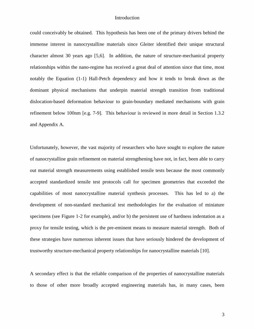
Figure 1-2 (a) Scanning electron micrograph of a dog-bone-shaped microsample used to
evaluate the tensile properties of nanocrystalline Cu produced by inert gas condensation [12].
The 4µm-deep indents (inset) were used as markers for the strain gauge but reportedly did not
affect the results. (b) 3mm-length specimens before and after tensile testing of electrodeposited
nanocrystalline Ni material batches A and B [13].
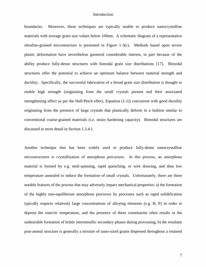
Figure 1-3 Schematic illustrations of typical microstructures produced by the pre-eminent
nanomaterials synthesis methods (a) nanopowders; (b) consolidated nanopowders; (c)
deformation-induced nanostructures; (d) nanograins crystallized from an amorphous phase; (e)
nanotwinned material; and (f) electrodeposited nanocrystalline material [courtesy of U. Erb].
Figure 1-4 (a) Young‟s Modulus of electrodeposited nanocrystalline Ni and NiP alloys as a
function of grain size [79]; (b) Young‟s and shear moduli of nanocrystalline Fe produced by
mechanical attrition expressed as ratios of the conventionally accepted, coarse-grained bulk
values. The dashed and solid curves correspond to a grain boundary thickness of 0.5 and 1nm,
respectively. The open circles show the E/Eo values of nanocrystalline Fe versus grain size [76].
Figure 1-5 Three models proposed to explain Hall-Petch behavior. Models due to (a) Cottrell
[92], (b) Li [93], and (c) Meyers and Ashworth [94]. Figure from ref. [95].
Figure 1-6 Schematic diagram of the variation of yield strength as a function of grain size [45].
Figure 1-7 Volume fractions of the total interface component, grain boundaries and triple
junctions, as a function of grain size, assuming a grain boundary width of 1nm [99].
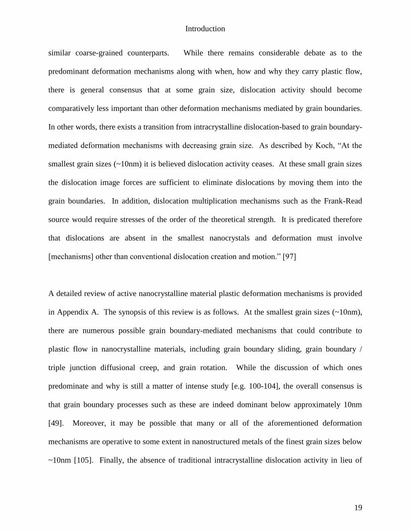
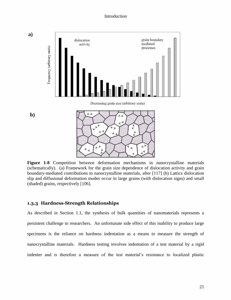
Figure 1-8 Competition between deformation mechanisms in nanocrystalline materials
(schematically). (a) Framework for the grain size dependence of dislocation activity and grain
boundary-mediated contributions to nanocrystalline materials, after [117] (b) Lattice dislocation
slip and diffusional deformation modes occur in large grains (with dislocation signs) and small
(shaded) grains, respectively [106].
Figure 1-9 Elongation-to-fracture data for (a) a variety of metals and alloys produced using a
range of synthesis methods [138], and (b) electrodeposited Ni-based materials (figure taken from
ref [140]).
Figure 1-10 (a) Deformation and fracture processes in a specimen with a bimodal structure
[147], (b) engineering stress–strain curves for pure Cu. Curve A, annealed, coarse grained Cu; B,
room temperature rolling to 95% cold work (CW); C, liquid-nitrogen temperature rolling to 93%
CW; D, 93% CW . 180 8C, 3 min.; and E, 93% CW . 200 8C, 3 min. Note the coexisting high
strength and large uniform plastic strain as well as large overall percentage elongation to failure
x
for curve E (bimodal structure) [148]; (c) Tensile curves of extruded nanocrystalline Al–7.5Mg
samples with varying concentrations of blended coarse-grained powder to create a bimodal
structure [149].
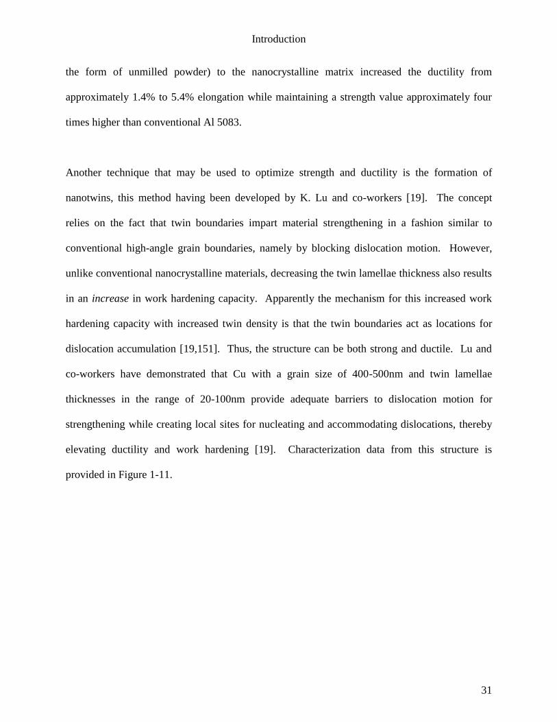
Figure 1-11 (top) Transmission electron microscopy (TEM) observations of the typical
microstructure in an as-deposited nanotwinned Cu sample. A bright field TEM image (A) and
the electron diffraction pattern (inset in (A)) show roughly equiaxed submicron-sized grains with
random orientations separated by high angle grain boundaries; (bottom) a typical tensile stress-
strain curve for the Cu sample with nano-twins in comparison with that for a coarse-grained
polycrystalline Cu (average grain size >100 µm) and a nanocrystalline Cu sample (mean grain
size ~ 30 nm). Inset shows the geometry of the tensile sample for the as-deposited nano-twin
sample [19].
Figure 1-12 Typical engineering stress-strain behaviour to fracture, point F. The “ultimate
tensile strength” is indicated at point M. The circular insets represent the geometry of the
deformed specimen at various points along the curve [61].
Figure 1-13 Illustration of diffuse necking and localized necking in a sheet tensile specimen
[152].
Figure 1-14 Photographs of the gauge sections of fractured tensile test coupons from (a) cold
rolled steel [155], and (b) cold rolled Al [157], illustrating localized necking and the 55° fracture
angle.
Figure 1-15 Schematic diagram of tensile sample geometries used in the current and previous
studies (Wang et al. [4], Zimmerman et al. [158], Dalla Torre et al. [13]) on electrodeposited
nanocrystalline materials as compared to the ASTM E8 standard subsize tensile test geometry
specification [11].
Figure 1-16 Tensile ductility (as measured by reduction in area) of a variety of dual-phase
copper alloys as a function of second phase volume fraction [159].
Figure 1-17 Elongation-to-fracture data for metals and alloys produced using a variety of one-
step and two-step processing methods, data from [139].
Figure 1-18 Tensile curves obtained for ball milled nanocrystalline Cu and coarse-grained Cu at
a strain rate of 10−3
s−1
[138].
Figure 1-19 Representative stress–strain curves for nanocrystalline and coarse-grained cobalt
(annealed at 800°C) at strain rates ε1 = 1 x 10⁻⁴
, ε2 = 5 x 10⁻⁴
, ε3 = 2.5 x 10⁻³
[161].
Figure 2-1 Side view schematic of the internal stress measurement apparatus showing the
initially flat Cu foil strip onto which the material in question is electrodeposited (shown as the
curved black line) clamped by a screw at the top of the fixture and permitted to bend naturally.
When the electrodeposited coating exhibits tensile residual stress, the direction of deflection is
opposite the case when the electrodeposit stress is compressive in nature (both cases are shown
xi
in the figure). The amount of deflection of the bottom edge of the foil is measured using a
graduated scale at the bottom of the apparatus, with this scale having been calibrated by the
manufacturer in such a way that a value for the electrodeposited coating residual stress level may
be calculated [2].
Figure 2-2 Photograph of typical specimens (Ni-6.4wt%Fe; 18nm average grain size) before
and after tensile testing in conformance with ASTM E8 [3]. Scale in cm.
Figure 3-1 Schematic diagram showing net-shape manufacturing of an electroformed product
[1].
Figure 3-2 Schematic diagrams showing the experimental set-up for pulsed current plating [2].
Figure 3-3 Schematic diagram and cross-sectional scanning electron micrograph of a coarse-
grained electrodeposit ((a) and (b)) compared to a nanocrystalline electrodeposit ((c) and (d))
[2,8].
Figure 3-4 Effect of overpotential (η) / current density (I) on critical crystal nucleation size (r)
[2].
Figure 3-5 „Processing-structure‟ relationship for pulsed electrocrystallization. Fundamental
mathematical expressions describing the physical phenomena linking the physically measureable
quantities (in ovals) exist as shown by the mechanisms between each oval. The links get
progressively weaker down the chain and are replaced by empirical relationships towards the end
[10].
Figure 3-6 Schematic diagram showing nucleation, growth, and surface diffusion during
electrocrystallization [11].
Figure 3-7 Nanocrystalline Ni-Fe electrodeposit grain size as a function of deposit chemical
composition, illustrating the significant grain refining effect of alloying in the electrodeposited
Ni-Fe binary system [13].
Figure 3-8 (a) Top-view schematic and (b) photograph of the electroforming apparatus used for
the Ni-Fe synthesis component of this work.
Figure 3-9 Schematic illustration of the square-wave pulsed electrodeposition waveform used in
the present study.
Figure 3-10 Photograph of a typical electroformed plate from which tensile specimens used in
this study were cut alongside a single tensile test specimen (scale in cm).
Figure 3-11 Internal stress of Ni electrodeposited from a standard Watts electrolyte as a function
of stress reliever concentration; values from (a) the literature [19]; and (b) the current study.
xii
Figure 3-12 The nature of benzoic acid sulfimide decomposition in the Watts Ni plating
electrolyte. Concentration of benzoic acid sulfimide along with two of its decomposition
products, o-toluene sulfonamide and benzamide, as a function of bath use as expressed by the
amount of electrical charge (Amp-hr) passed through the solution per unit volume [20].
Figure 3-13 Average grain size of electrodeposited nanocrystalline Ni as a function of
electrolyte grain refiner concentration as compared to that from a previous study [12].
Figure 3-14 Schematic illustration of common processing artifacts encountered in
electrodeposition [20].
Figure 3-15 Cross-sectional optical micrograph of an electroformed plate containing nodular /
dendritic growth. Deposit growth direction is from bottom to top.
Figure 3-16 (a,b) SEM Analysis of the fracture face of a nanocrystalline Ni tensile specimen
synthesized using an electroforming process replenished with water from a malfunctioning de-
ionized water system indicating the presence of particulate contamination; (c) EDX spot analysis
of the Ca particulate (images courtesy of Peter Lin, Integran Technologies Inc.).
Figure 3-17 Photograph of representative electroformed nanocrystalline Ni plates produced
before and after implementing processing artifact minimization (courtesy of Peter Lin, Integran
Technologies Inc.).
Figure 3-18 Cross-sectional optical micrograph of an electroformed plate containing hydrogen
pitting. Deposit growth direction is from bottom to top.
Figure 3-19 TEM characterization data of a nanocrystalline Ni (31 ± 9nm average grain size)
sample showing a (a) bright field image, (b) selected area diffraction pattern, and (c) grain size
distribution.
Figure 3-20 Typical XRD diffraction profiles (Co Kα radiation) for representative pure Ni
(38nm grain size) and Ni-46.8wt% Fe (10nm grain size) nanomaterials alongside the calculated
random profile for Ni.
Figure 3-21 TEM characterization data of a Ni-47.3%Fe (9nm average grain size) sample
showing a (a) bright field image, (b) dark field image, (c) selected area diffraction pattern and (d)
grain size distribution [24].
Figure 3-22 TEM bright field image of specimen AE065 indicating an 80nm average grain size
and a large concentration of faulted regions [courtesy of G. Cingara].
Figure 4-1 Tensile engineering stress-strain data from six individual specimens cut from a
single plate of material produced using (a) an early scale-up stage electroforming process
alongside (b) data from six individual specimens cut from an otherwise identical plate of material
produced using a later generation process with much stricter processing artifact control.
xiii
Figure 4-2 Scanning electron micrograph images of the fracture surfaces of nanocrystalline Ni
tensile samples produced using (a) an early scale-up stage electroforming process alongside (b)
an otherwise identical plate of material produced using a later generation process with much
stricter processing artifact control.
Figure 4-3 Quasi-static tensile strain-to-fracture and uniform plastic strain as a function of plate
thickness for nanocrystalline Ni specimens of similar microstructure, areal shape and processing
method.
Figure 4-4 Scanning electron microscopy (SEM) images from a typical thin foil (0.05mm
thickness) nanocrystalline Ni sample after tensile testing illustrating the combination of (a) brittle
macroscopic fracture morphology and (b) highly localized necking.
Figure 4-5 The geometrical dependency of tensile elongation-to-fracture of nanocrystalline Ni
(present study) compared to that exhibited by other standard engineering materials (data from ref
[21]).
Figure 4-6 (a) Two-parameter Weibull fit to strain-to-fracture data from nanocrystalline Ni
specimens varying thickness from 0.030 to 2.5mm; (b) schematic diagram depicting the
superposition of the geometrical / surface and volume flaw effects that control the tensile strain-
to-fracture variability of electrodeposited nanocrystalline Ni.
Figure 4-7 Photographs of the gauge sections of fractured tensile test coupons from (a) the
current study (0.5mm-thick), (b) cold rolled steel [22], and (c) cold rolled Al [23], illustrating the
55° fracture angle resulting from localized necking deformation [24].
Figure 4-8 Optical micrographs (left) of the gauge section of representative specimens
illustrating the transition in failure mode from plane strain to plane stress with increasing sample
thickness (t) paired with SEM images (right) of the corresponding fracture surfaces: (a) <0.1mm,
(b) 0.1 – 0.5mm, (c) 0.8 -1mm, (d) 2-2.5mm. The gauge width (w) of each specimen shown is
approximately 6.3mm. Grain size = 25 nm.
Figure 4-9 Representative tensile engineering stress-strain curves with average grain sizes and
compositions provided in the legend. All samples electrodeposited except for the Ni-200
standard.
Figure 4-10 Two-parameter Weibull fit to strain-to-fracture data illustrating the differences in
statistical variability between the samples of approximately 1mm thickness (crosses) and the
samples of varying thickness from 0.030 to 2.5mm (squares).
Figure 4-11 Maximum uniform plastic and non-uniform strain distributions for 116
nanocrystalline Ni-based specimens of equivalent geometry and spanning average grain size
values from 10 to 80nm.
Figure 4-12 Maximum uniform plastic strain plotted as a function of yield strength which serves
as a proxy for grain size as per the Hall-Petch relationship.
xiv
Figure 4-13 Predicted variation of the strain at the onset of necking in uniaxial tension of ferritic
steel with different grain sizes along with comparison to experimental results [30].
Figure 4-14 Hardening capacity (h = σUTS / σY) plotted as a function of yield strength which
serves as a proxy for grain size as per the Hall-Petch relationship for 116 nanocrystalline Ni-
based specimens of equivalent geometry and spanning average grain size values from 10 to
80nm.
Figure 4-15 Ductile fracture in nanocrystalline materials that occurs through formation of
nanocracks, their transformation into pores, growth of pores and formation of local necks
between large pores [31].
Figure 5-1 Vickers hardness as a function of ultimate tensile strength data for carbon and alloy
steels in the annealed, normalized, and quenched-and-tempered conditions [12].
Figure 5-2 Stress strain curves for typical nanocrystalline Ni-based electrodeposits recorded in
conformance with ASTM E8M-01.
Figure 5-3 Hardness as a function of tensile yield strength measured for a wide range of
electrodeposited nanocrystalline materials.
Figure 5-4 Hardness as a function of ultimate tensile strength measured for a wide range of
electrodeposited nanocrystalline materials.
Figure 5-5 The ratio of hardness to (a) yield strength, and (b) ultimate tensile strength as a
function of grain size, as measured by XRD line broadening.
Figure 5-6 The ratio of hardness to (a) yield strength, and (b) ultimate tensile strength as a
function of grain size, as measured by XRD line broadening.
Figure 5-7 The influence of the material strain hardening exponent n on the calculated ratios of
hardness to ultimate tensile strength (using the model of Tabor [25]; Equation (5-1)) and
hardness to yield strength (using the models of Cahoon et al. [30] (Equation (5-2)) and Gao [28]
(Equation (5-3))).
Figure 5-8 The ratio of hardness to ultimate tensile strength as a function of tensile elongation
for (a) all specimens analyzed, and (b) only specimens displaying a distinct necking instability
failure mode.
Figure 5-9 A comparison of material yield strength estimates generated using σY = HV / 3
(Equation (1-5)) to the models of Cahoon et al. [30] (Equation (5-2)) and Gao [28] (Equation (5-
3)).
Figure 7-1: Minimum specimen thickness required for trustworthy measurement of the plane
strain fracture toughness, KIc, of a material as per Equation (7-1).
xv
Figure A-1 Proposed deformation mechanism of electrodeposited nanocrystalline Ni of 20nm
grain size based upon the results of in situ TEM tensile testing. Grain boundary sliding
transforms into crystal lattice rotation in neighboring grains. a) Before plastic deformation, the
materials possessed high angle grain boundaries; b) shear of two nano-sized grains 1 and 2 by
gliding grain boundary dislocations, and subsequent occurrence of the crystal lattice rotation in
the neighboring nanocrystalline grain 3 by climbing GB dislocations; c) multiple grain rotations
leading to grain agglomeration; d) a large grain formed with sub-boundaries (highlighted by
dotted lines) due to incomplete grain coalescence [8].
Figure A-2 Computer generated nanocrystalline Ni sample with a mean grain size of 12 nm
synthesized using the Voronoi construction [13].
Figure A-3 The dislocation mechanism suggested by molecular dynamics for f.c.c. metals: a
leading partial is nucleated (a), and a trailing partial follows (b), the dislocation travelling
through the grain (c), being finally absorbed in opposite GBs (d) [13].
Figure A-4 Grain boundary sliding along a bi-crystal boundary with steps and facets. (a) Initial
state. (b) Non-accommodated grain boundary sliding results in the formation of regions (grey)
where neighbouring grains interpenetrate and regions (white) where voids are formed. (c)
Elastic accommodation. (d) Diffusional accommodation. (e) Lattice slip accommodation. (f)
Accommodating local migration of grain boundaries [24].
Figure A-5 2D schematic of a grain arrangement in a (A) nano- and (B) polycrystalline material.
A mesoscopic planar interface can be formed by grain boundary migration. Atoms located in the
darker regions have to be re-arranged in the process of grain boundary sliding [25].
Figure A-6 Twin deformation conducted by regularly arranged partial dislocations emitted from
a grain boundary [24].
Figure A-7 Schematic representation of diffusional creep. Self-diffusion should result in plastic
flow if matter is carried from boundaries subject to compressive stress (vertical boundaries) over
to boundaries under a tensile stress (horizontal boundaries) [38].
Figure A-8 A deformation map for pure Ni showing the effect of grain refinement from 32µm to
10nm (finer solid lines) [40].
Figure A-9 Grain rotation in a polycrystalline solid. (a) Initial state. (b) Non-accommodated
grain rotation results in the formation of small regions (black regions near boundaries of rotated
grain) where neighbouring grains interpenetrate and small regions (white regions near
boundaries of rotated grain) where voids are formed. (c) Accommodation by bulk diffusion. (d)
Accommodation by grain boundary diffusion [24]. Figure A-10 Competition between deformation mechanisms in nanocrystalline materials
(schematically). (a) Framework for the grain size dependence of dislocation activity and grain
boundary-mediated contributions to nanocrystalline materials, after [47] (b) Lattice dislocation

xvi
slip and diffusional deformation modes occur in large grains (with dislocation signs) and small
(shaded) grains, respectively [24].

xvii
List of Appendices
Appendix A - Plastic Deformation Mechanisms in Nanocrystalline Materials: An Overview
1
Chapter 1 Introduction
1.1 Background & Motivation for Study
A significant portion of materials science is concerned with the development of synthesis-
structure-property relationships. What are the important properties of a material (e.g.
mechanical, magnetic, electrical, thermal, etc.) and what is the nature of their dependency on the
structure of that material? Equipped with an understanding of synthesis-structure-property
relationships for a given material, the engineer may then effectively design methods for
fabricating that material so that it can be used in practical applications.
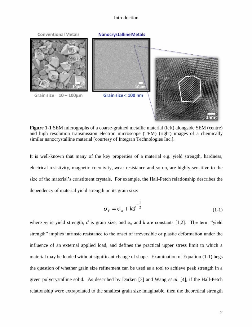
Most metallic materials are comprised of a fully dense aggregate of crystals or grains known as a
polycrystalline structure. A scanning electron microscope (SEM) image showing the
microstructure of a typical polycrystalline metallic material is shown at the left-hand side of
Figure 1-1. The interfaces between the grains near the surface of this particular specimen have
been chemically etched to accentuate its polycrystalline character, but otherwise the material is
fully-dense. The diameter of the crystals of this material varies between roughly 10-30µm,
which is typical for a conventional polycrystalline engineering material. On the other hand, new
methods exist to create materials with much smaller crystals. A nanocrystalline material is
rather arbitrarily defined as a polycrystalline material that possesses an average grain size below
0.1µm (or 100nm), and an example of such a microstructure is shown on the right-hand side of
Figure 1-1.
Introduction
2
10µm 10µm
Conventional Metals Nanocrystalline Metals
Grain size = 10 – 100µm Grain size < 100 nm
1nm
Figure 1-1 SEM micrographs of a coarse-grained metallic material (left) alongside SEM (centre)
and high resolution transmission electron microscope (TEM) (right) images of a chemically
similar nanocrystalline material [courtesy of Integran Technologies Inc.].
It is well-known that many of the key properties of a material e.g. yield strength, hardness,
electrical resistivity, magnetic coercivity, wear resistance and so on, are highly sensitive to the
size of the material’s constituent crystals. For example, the Hall-Petch relationship describes the
dependency of material yield strength on its grain size:
2
1
kdoY (1-1)
where σY is yield strength, d is grain size, and σo and k are constants [1,2]. The term “yield
strength” implies intrinsic resistance to the onset of irreversible or plastic deformation under the
influence of an external applied load, and defines the practical upper stress limit to which a
material may be loaded without significant change of shape. Examination of Equation (1-1) begs
the question of whether grain size refinement can be used as a tool to achieve peak strength in a
given polycrystalline solid. As described by Darken [3] and Wang et al. [4], if the Hall-Petch
relationship were extrapolated to the smallest grain size imaginable, then the theoretical strength
Introduction
3
could conceivably be obtained. This hypothesis has been one of the primary drivers behind the
immense interest in nanocrystalline materials since Gleiter identified their unique structural
character almost 30 years ago [5,6]. In addition, the nature of structure-mechanical property
relationships within the nano-regime has received a great deal of attention since that time, most
notably the Equation (1-1) Hall-Petch dependency and how it tends to break down as the
dominant physical mechanisms that underpin material strength transition from traditional
dislocation-based deformation behaviour to grain-boundary mediated mechanisms with grain
refinement below 100nm [e.g. 7-9]. This behaviour is reviewed in more detail in Section 1.3.2
and Appendix A.
Unfortunately, however, the vast majority of researchers who have sought to explore the nature
of nanocrystalline grain refinement on material strengthening have not, in fact, been able to carry
out material strength measurements using established tensile tests because the most commonly
accepted standardized tensile test protocols call for specimen geometries that exceeded the
capabilities of most nanocrystalline material synthesis processes. This has led to a) the
development of non-standard mechanical test methodologies for the evaluation of miniature
specimens (see Figure 1-2 for example), and/or b) the persistent use of hardness indentation as a
proxy for tensile testing, which is the pre-eminent means to measure material strength. Both of
these strategies have numerous inherent issues that have seriously hindered the development of
trustworthy structure-mechanical property relationships for nanocrystalline materials [10].
A secondary effect is that the reliable comparison of the properties of nanocrystalline materials
to those of other more broadly accepted engineering materials has, in many cases, been
Introduction
4
impossible to carry out because the relevant properties have been measured using fundamentally
dissimilar tests. The end result is that the materials selection process in engineering design has
also been rendered unreliable because the standard tests cannot be performed. Therefore, the
primary objective of this work has been the development of a synthesis method to produce
specimens large enough for testing in accordance with ASTM E8 [11], arguably the most widely
used mechanical test in North America. In this manner, the resultant test data might be more
reliably compared to data from other well-known engineering materials. Another objective has
been to evaluate the validity of the hardness-strength relationships most commonly used in the
study of nanocrystalline materials. In doing so, two of the most prevalent issues with effective
mechanical property characterization of nanocrystalline materials (non-standard tensile test
geometries and substitution of hardness indentation for strength testing) could be systematically
addressed.
Figure 1-2 (a) Scanning electron micrograph of a dog-bone-shaped microsample used to
evaluate the tensile properties of nanocrystalline Cu produced by inert gas condensation [12].
The 4µm-deep indents (inset) were used as markers for the strain gauge but reportedly did not
affect the results. (b) 3mm-length specimens before and after tensile testing of electrodeposited
nanocrystalline Ni material batches A and B [13].
a)
Introduction
5
1.2 Processing of Nanocrystalline Materials
Specimen size effects aside, past attempts to obtain a broader picture of the intrinsic mechanical
properties of nanocrystalline materials have also been challenging because the process-related
material characteristics (e.g. microstructural variability, porosity, impurities, processing artifacts)
have generally not been rigorously accounted for in the rationalization of the observed response
to deformation. Nanocrystalline materials can be produced using a relatively large number of
synthesis routes resulting in a huge diversity of structures from these often fundamentally
dissimilar processing methods. For example, “two-step” processes typically involve the
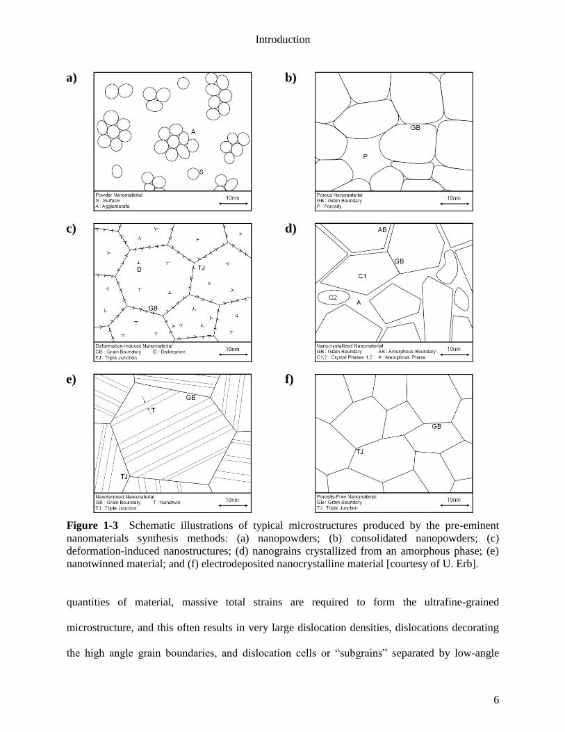
production of a nanopowder followed by some sort of consolidation process. See Figure 1-3(a)
for a schematic representation of a nanomaterial powder feedstock alongside that of the
consolidated structure in Figure 1-3(b). The most common synthesis technique examples for
such materials include inert gas condensation methods, mechanical attrition by ball milling, and
sol-gel chemical processing. Significant progress has recently been made in the reliable
synthesis and consolidation of ball-milled nanomaterials in particular [14,15]. However, after
consolidation of the nano-sized particulate, these materials invariably retain some degree of
small-scale porosity, which is known to have a marked influence on the mechanical properties,
most notably the elastic properties [16].
On the other hand, “single-step” processing techniques output ultrafine-grained material in one
step without the need for subsequent powder consolidation. The most popular examples are
based upon either severe plastic deformation (e.g. high pressure torsion (HPT), equal channel
angular pressing (ECAP), and accumulative roll-bonding (ARB)), crystallization of amorphous
precursors or electrodeposition. While severe plastic deformation is capable of producing bulk
Introduction
6
Figure 1-3 Schematic illustrations of typical microstructures produced by the pre-eminent
nanomaterials synthesis methods: (a) nanopowders; (b) consolidated nanopowders; (c)
deformation-induced nanostructures; (d) nanograins crystallized from an amorphous phase; (e)
nanotwinned material; and (f) electrodeposited nanocrystalline material [courtesy of U. Erb].
quantities of material, massive total strains are required to form the ultrafine-grained
microstructure, and this often results in very large dislocation densities, dislocations decorating
the high angle grain boundaries, and dislocation cells or “subgrains” separated by low-angle
a) b)
c)
e)
d)
f)
Introduction
7
boundaries. Moreover, these techniques are typically unable to produce nanocrystalline
materials with average grain size values below 100nm. A schematic diagram of a representative
ultrafine-grained microstructure is presented in Figure 1-3(c). Methods based upon severe
plastic deformation have nevertheless garnered considerable interest, in part because of the
ability produce fully-dense structures with bimodal grain size distributions [17]. Bimodal
structures offer the potential to achieve an optimum balance between material strength and
ductility. Specifically, the successful fabrication of a broad grain size distribution is thought to
enable high strength (originating from the small crystals present and their associated
strengthening effect as per the Hall-Petch effect, Equation (1-1)) concurrent with good ductility
originating from the presence of large crystals that plastically deform in a fashion similar to
conventional coarse-grained materials (i.e. strain hardening capacity). Bimodal structures are
discussed in more detail in Section 1.3.4.1.
Another technique that has been widely used to produce fully-dense nanocrystalline
microstructures is crystallization of amorphous precursors. In this process, an amorphous
material is formed by e.g. melt-spinning, rapid quenching, or wire drawing, and then low
temperature annealed to induce the formation of small crystals. Unfortunately, there are three
notable features of the process that may adversely impact mechanical properties: a) the formation
of the highly non-equilibrium amorphous precursor by processes such as rapid solidification
typically requires relatively large concentrations of alloying elements (e.g. B, P) in order to
depress the eutectic temperature, and the presence of these constituents often results in the
undesirable formation of brittle intermetallic secondary phases during processing, b) the resultant
post-anneal structure is generally a mixture of nano-sized grains dispersed throughout a retained
Introduction
8
amorphous matrix – see Figure 1-3(d), and c) the cooling rates required to achieve the desired
microstructure are so high (typically on the order of 106 K/s) that only thin foils can be produced.
Nanocrystalline materials produced by this route typically exhibit very limited ductility but have
found industrial application as soft magnetic materials [18].
Another interesting microstructure is the nanotwinned structure, pioneered by Lu and co-workers
[19]. A representative schematic of this microstructure is shown in Figure 1-3(e), and is
characterized by a high density of nanoscale growth twins embedded within individual grains. In
the case of Cu, the grain sizes are typically on the order of 400-500nm while the twin lamellae
thickness ranges from approximately 20-100nm. This structure appears to hold considerable
promise for optimizing both strength and ductility [20]. It should also be noted that pulsed
current electrodeposition is one of the processing methods that has been used to achieve the
nanotwinned structure [21].
Finally, Figure 1-3(f) contains a schematic illustration of the structure employed in the current
study, namely single phase structures produced by pulsed current electrodeposition. These
microstructures are characterized by an equiaxed grain shape and a relatively narrow log-normal
grain size distribution. A notable characteristic is that, unlike most other processes,
electrodeposition permits the synthesis of a wide range of grain sizes, in some cases covering the
entire structural range from >10µm through to amorphous, from a given metal or alloy system by
control of processing parameters. In addition, because electrodeposition is a single-step process
that typically yields fully-dense structures, the potential to eliminate or at least minimize
processing artifacts such as porosity exists.
Introduction
9
1.3 Mechanical Properties of Nanocrystalline Materials: An Overview
Owing to the fact that the Hall-Petch effect is the primary driver behind the interest in
nanocrystalline materials, a tremendous amount of work has been directed towards the study of
their mechanical properties. The key findings have been summarized in numerous books [e.g.
22-27], conference proceedings [e.g. 28-35], viewpoint sets [e.g. 36-38], and review articles [e.g.
9,17,39-60]. A review of the plastic deformation mechanisms thought to be active in
nanocrystalline materials is provided in Appendix A. The objective of this section is to provide a
general overview of this literature as it relates to the mechanical properties of nanocrystalline
materials, with particular emphasis on materials produced by electrodeposition.
1.3.1 Elastic Properties
By virtue of their ultra-fine grained microstructures, nanocrystalline materials exhibit high
strength and this characteristic makes them suitable candidates for load-bearing applications.
However, the vast majority of engineering components are intended for continued use over
extended time periods, and are therefore designed such that all constituent structural members
are safely and predictably loaded strictly within their elastic regimes, and do not experience any
permanent change in shape resulting from irreversible plastic deformation in service. Within the
elastic regime, the intrinsic capability of a material to withstand deformation is commonly
known as its “stiffness”. From this information, one may derive the extent to which the material
will deform (“elastic strain”) when loaded under some given stress level within the elastic regime
or, conversely, the resistance to deformation (“elastic stress”) upon application of a given elastic
Introduction
10
strain. Consequently, the elastic stiffness properties of a material represent some of the most
practically relevant mechanical characteristics of a structural engineering material.
On an atomic scale, elastic strain is manifested as small changes in the interatomic spacing and
the stretching of the interatomic bonds [e.g. 61]. In other words, the macroscopic Young’s
modulus is ultimately a reflection of the interatomic bonding forces, assuming no other
contributions to measured strain. Given that the values of a material’s elastic constants reflect
the bonding nature of its constituent atoms, it seems logical to expect that nanocrystalline
materials would exhibit different moduli of elasticity compared to coarse-grained polycrystalline
solids because of the high volume fraction of atoms located at or near the grain boundaries, triple
junctions, and quadruple nodes. In particular, since the degree of atomic structural disorder is
greater within a grain boundary as compared to the crystal lattice, the average atomic distance
within it is generally known to be larger [62]. It could then be concluded that the grain boundary
as a whole exhibits a lower bond strength and, therefore, have local elastic moduli values lower
than those of the lattice. On the other hand, a computer simulation study of a Σ5 Cu grain
boundary performed by Wolf and co-workers [63] resulted in exactly the opposite conclusion.
Namely, an increase in Young’s modulus was observed across the grain boundary. This was
attributed to the asymmetry of the interatomic potential, whereby shortened atomic distances are
weighted more heavily than expanded distances and hence the local elastic stiffness of a grain
boundary may be enhanced by the relatively low number of interatomic distances smaller than
the equilibrium distance.
Introduction
11
In general, the question of how a material’s internal interfaces contribute to its bulk elasticity has
been a matter of intense debate for many years. Most of the early work seemed to suggest that
the presence of a significant fraction of interfacial atoms induces a huge effect on the elasticity of
polycrystalline solids. Specifically, the Young’s moduli of many nanocrystalline materials were
found to be significantly lower than those of their coarse-grained equivalents, up to 50% in some
cases [6,64-70]. However, it was subsequently demonstrated that this drop was due in many
cases to material porosity, the influence of which is thought to be substantially stronger than that
of grain size. One of the first studies that aimed to quantify this effect was carried out by Krstic
et al. [16], who developed a model to describe the elastic response of consolidated
nanocrystalline powders containing residual porosity resulting from the compaction stage of
processing. The aforementioned E drop was deemed by the authors to be a natural result of
porosity rather than severe grain refinement, this being corroborated by the fact that
electrodeposited fully dense 7 nm grain size Ni-1.2 wt.%P exhibited essentially the same
Young’s modulus (E = 225 GPa) as that of a coarse-grained Ni reference sample (E = 221 GPa)
[71].
Several others have followed similar lines of reasoning in an attempt to quantitatively determine
the effect of grain size on elastic response. Fougere et al. [72], for example, used both Krstic’s
model and that of Boccaccini et al. [73] in order to fit Young’s modulus as a function of pore
volume fraction for a large number of Inert Gas Condensed (IGC) Fe samples, ultimately
drawing the conclusion that porosity is the dominant microstructural feature in determining the
extent of the observed decrement in E. Kim and Bush [74] also carried out similar calculations
using Budiansky’s method [75] to predict the properties of composite materials comprised of a
Introduction
12
random mixture of isotropic constituents, pores being treated as a separate phase of zero-valued
bulk and shear moduli. Considering both porosity and grain size effects, they also concluded that
the contribution of the grain size could be ignored compared with the influence of porosity.
To further illustrate the problems associated with consolidated nanocrystals, Shen et al. [76]
pointed out that the Young’s modulus of nanocrystalline Pd with an 8 nm grain size produced by
IGC was reported to be 47 and 88 GPa in two different studies. This variation likely resulted
from differences in the sample porosity brought about by variations in the condensation and/or
compaction parameters. Upon careful application of nanoindentation to porosity-free locations
on their mechanically-milled samples, these researchers observed essentially no difference in
Young’s modulus between 17 to 26 nm grain size nanocrystalline Fe, Cu, Ni and Cu-Ni alloys
and the corresponding chemically equivalent coarse-grained polycrystalline materials. In another
study of the elastic response of nanomaterials, ultrasonic techniques were employed in order to
characterize fine-grained (250 nm) Cu synthesized via severe plastic deformation [77]. The
authors calculated a Young’s modulus drop and attributed this to non-equilibrium grain
boundaries. Subsequently, detailed crystallographic texture studies carried out on the same
material revealed that this drop was, in fact, a result of the preferred crystallographic orientation
rather than any low modulus non-equilibrium grain boundary phase [78].
Hence, it can be concluded that in any discussion of the elasticity of nanomaterials, the possible
effects linked to the chosen synthesis route (i.e. porosity), crystallographic texture, or any other
structural feature that could play a role in the interpretation of elastic response measurements
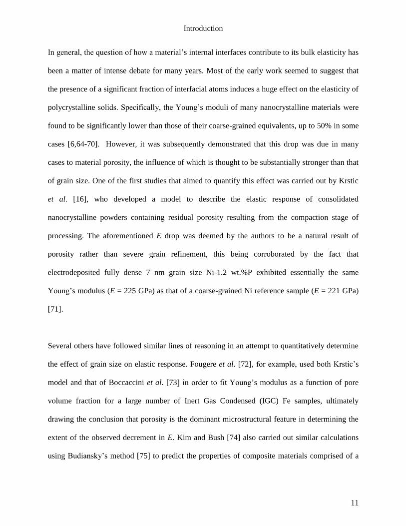
must be considered. As it pertains specifically to the effect of grain size, Figure 1-4 captures the
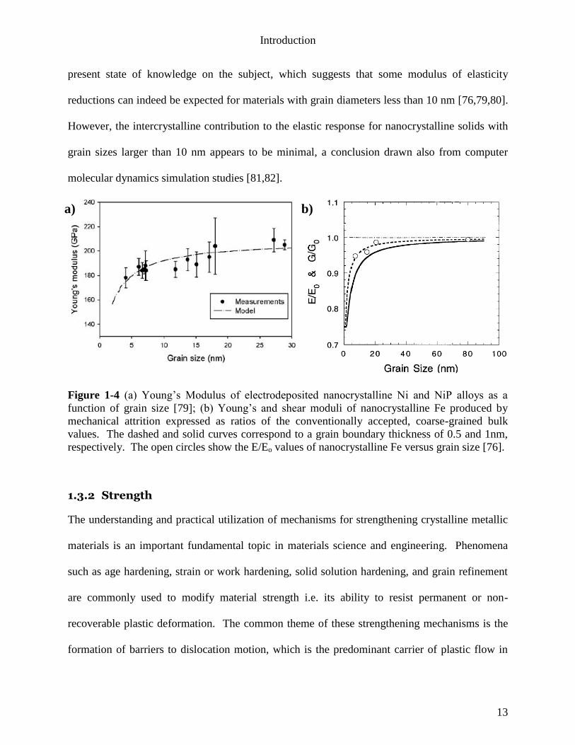
Introduction
13
present state of knowledge on the subject, which suggests that some modulus of elasticity
reductions can indeed be expected for materials with grain diameters less than 10 nm [76,79,80].
However, the intercrystalline contribution to the elastic response for nanocrystalline solids with
grain sizes larger than 10 nm appears to be minimal, a conclusion drawn also from computer
molecular dynamics simulation studies [81,82].
Figure 1-4 (a) Young’s Modulus of electrodeposited nanocrystalline Ni and NiP alloys as a
function of grain size [79]; (b) Young’s and shear moduli of nanocrystalline Fe produced by
mechanical attrition expressed as ratios of the conventionally accepted, coarse-grained bulk
values. The dashed and solid curves correspond to a grain boundary thickness of 0.5 and 1nm,
respectively. The open circles show the E/Eo values of nanocrystalline Fe versus grain size [76].
1.3.2 Strength
The understanding and practical utilization of mechanisms for strengthening crystalline metallic
materials is an important fundamental topic in materials science and engineering. Phenomena
such as age hardening, strain or work hardening, solid solution hardening, and grain refinement
are commonly used to modify material strength i.e. its ability to resist permanent or non-
recoverable plastic deformation. The common theme of these strengthening mechanisms is the
formation of barriers to dislocation motion, which is the predominant carrier of plastic flow in
b) a)
Introduction
14
the vast majority of coarse-grained polycrystalline metallic materials at low temperatures. In age
hardening, for instance, precipitates are formed within the matrix lattice and the size, density
and/or degree of coherency of these secondary phases is controlled in order to optimize their
effective resistance to dislocation glide within the lattice of the matrix phase. In the case of
strain hardening, the material is plastically deformed or “worked” to generate high
concentrations of dislocations within the grain interiors. These dislocations then hinder the
motion of other dislocations when the material is mechanically loaded, with the end result being
that the strength of the strain hardened material is ultimately dependent upon its dislocation
concentration in a fashion analogous to the Hall-Petch relationship as follows:
2
1
Ki (1-2)
where ρ is the measured dislocation density in terms of dislocation length per unit volume, σ is
the measured flow stress, K is a constant, and σi is the stress obtained when ρ½ is extrapolated to
zero [83].
It is interesting to note that a relationship similar to Equations (1-1) and (1-2) is also observed for
laminate materials consisting of layers with thickness t [84-87]:
2
1
tk tt (1-3)
where σt and kt are constants.
In the case of grain refinement, the formation of smaller crystals brings with it a commensurate
increase in the volume fraction of interfaces between those crystals, and these interfaces act as
barriers to dislocation glide. Thus, finer grained materials possess more barriers to dislocation
Introduction
15
motion and are stronger than chemically similar coarser grained materials. Interestingly, the
specific mechanisms that underpin the Hall-Petch effect in conventional coarse-grained
polycrystalline metallic materials are still a matter of debate some 60 years after the behaviour
was first quantified [e.g. 88-91]. However, the effect is generally explained by an external
stress-induced pile-up of dislocations in one grain producing a stress concentration that activates
a (e.g. Frank-Read) dislocation source in an adjacent grain [92]. Alternative mechanisms involve
the activation of dislocation sources at grain boundary ledges [93], elastic/plastic incompatibility
stresses between neighbouring grains giving rise to the generation of dislocations that effectively
form a hardened reinforcing “second-phase” network [94], and so on. Schematic illustrations of
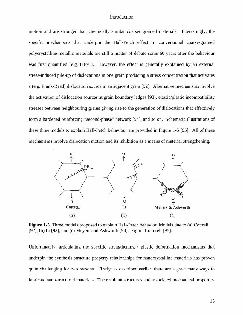
these three models to explain Hall-Petch behaviour are provided in Figure 1-5 [95]. All of these
mechanisms involve dislocation motion and its inhibition as a means of material strengthening.
Figure 1-5 Three models proposed to explain Hall-Petch behavior. Models due to (a) Cottrell
[92], (b) Li [93], and (c) Meyers and Ashworth [94]. Figure from ref. [95].
Unfortunately, articulating the specific strengthening / plastic deformation mechanisms that
underpin the synthesis-structure-property relationships for nanocrystalline materials has proven
quite challenging for two reasons. Firstly, as described earlier, there are a great many ways to
fabricate nanostructured materials. The resultant structures and associated mechanical properties
Introduction
16
are typically quite sensitive to the synthesis parameters and concomitant processing artifacts.
De-coupling the effects of the nanostructure from the method used to create it is typically very
difficult and so this has impeded the development of our understanding of the operative
nanocrystalline material deformation mechanisms which have heretofore been theoretically
developed primarily on the basis of structural considerations only. Secondly, because the
deformation mechanisms are operating at the near-atomic scale, their direct observation has been
difficult to accomplish. For instance, in the case of high resolution TEM evaluation of
nanocrystalline materials, the small crystal size results in overlapping of grains in the TEM foil,
making in situ observations of mechanically loaded nano-sized crystals quite challenging. Even
in those cases where individual nano-sized grains can be successfully resolved and plastically
deformed in the TEM, the relevance of thin foil deformation mechanisms to bulk deformation
may be questionable due to surface effects. Therefore, while numerous attempts to reveal the
dominant nanocrystalline material deformation mechanisms have been made, our inability to
“see” the deformation mechanisms in operation without great difficulty has definitely impeded
the undertaking.
Nevertheless, this topic has received considerable attention and the primary goal of this section is
to highlight the most important conclusions drawn so far. Before doing so, it is important to
summarize the key macroscale strength and hardness observations that form the basis for this
field of study:
1. The yield strength and hardness of nanocrystalline materials are extremely high. The
yield strength of a metallic nanocrystalline solid is typically 5-7 times its chemically
equivalent coarse-grained counterpart, while its hardness may be 3-10 times greater; and
Introduction
17
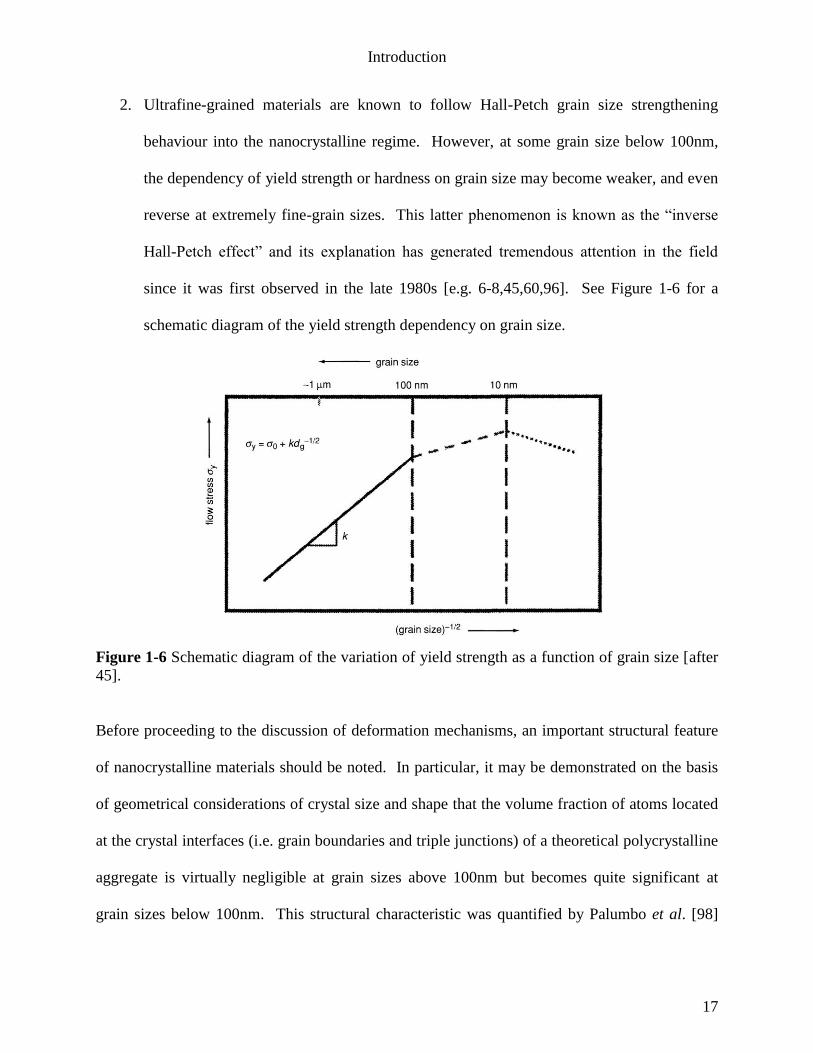
2. Ultrafine-grained materials are known to follow Hall-Petch grain size strengthening
behaviour into the nanocrystalline regime. However, at some grain size below 100nm,
the dependency of yield strength or hardness on grain size may become weaker, and even
reverse at extremely fine-grain sizes. This latter phenomenon is known as the “inverse
Hall-Petch effect” and its explanation has generated tremendous attention in the field
since it was first observed in the late 1980s [e.g. 6-8,45,60,96]. See Figure 1-6 for a
schematic diagram of the yield strength dependency on grain size.
Figure 1-6 Schematic diagram of the variation of yield strength as a function of grain size [after
45].
Before proceeding to the discussion of deformation mechanisms, an important structural feature
of nanocrystalline materials should be noted. In particular, it may be demonstrated on the basis
of geometrical considerations of crystal size and shape that the volume fraction of atoms located
at the crystal interfaces (i.e. grain boundaries and triple junctions) of a theoretical polycrystalline
aggregate is virtually negligible at grain sizes above 100nm but becomes quite significant at
grain sizes below 100nm. This structural characteristic was quantified by Palumbo et al. [98]
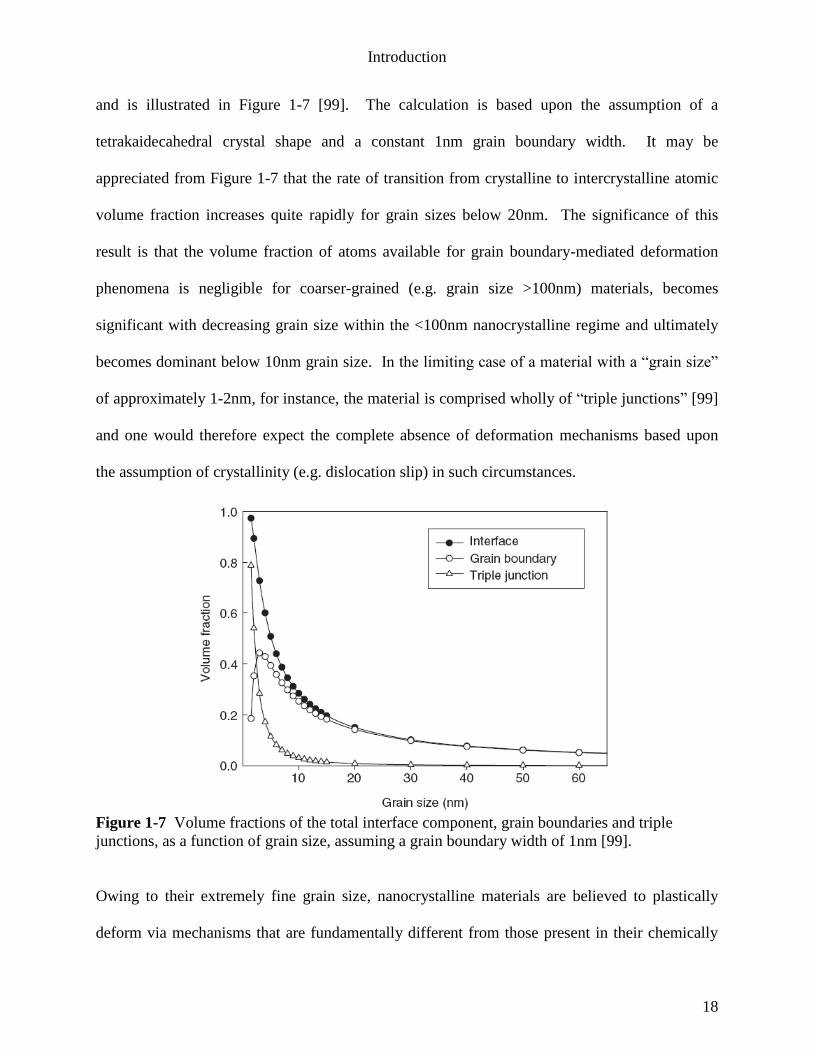
Introduction
18
and is illustrated in Figure 1-7 [99]. The calculation is based upon the assumption of a
tetrakaidecahedral crystal shape and a constant 1nm grain boundary width. It may be
appreciated from Figure 1-7 that the rate of transition from crystalline to intercrystalline atomic
volume fraction increases quite rapidly for grain sizes below 20nm. The significance of this
result is that the volume fraction of atoms available for grain boundary-mediated deformation
phenomena is negligible for coarser-grained (e.g. grain size >100nm) materials, becomes
significant with decreasing grain size within the <100nm nanocrystalline regime and ultimately
becomes dominant below 10nm grain size. In the limiting case of a material with a “grain size”
of approximately 1-2nm, for instance, the material is comprised wholly of “triple junctions” [99]
and one would therefore expect the complete absence of deformation mechanisms based upon
the assumption of crystallinity (e.g. dislocation slip) in such circumstances.
Figure 1-7 Volume fractions of the total interface component, grain boundaries and triple
junctions, as a function of grain size, assuming a grain boundary width of 1nm [99].
Owing to their extremely fine grain size, nanocrystalline materials are believed to plastically
deform via mechanisms that are fundamentally different from those present in their chemically
Introduction
19
similar coarse-grained counterparts. While there remains considerable debate as to the
predominant deformation mechanisms along with when, how and why they carry plastic flow,
there is general consensus that at some grain size, dislocation activity should become
comparatively less important than other deformation mechanisms mediated by grain boundaries.
In other words, there exists a transition from intracrystalline dislocation-based to grain boundary-
mediated deformation mechanisms with decreasing grain size. As described by Koch, “At the
smallest grain sizes (~10nm) it is believed dislocation activity ceases. At these small grain sizes
the dislocation image forces are sufficient to eliminate dislocations by moving them into the
grain boundaries. In addition, dislocation multiplication mechanisms such as the Frank-Read
source would require stresses of the order of the theoretical strength. It is predicated therefore
that dislocations are absent in the smallest nanocrystals and deformation must involve
[mechanisms] other than conventional dislocation creation and motion.” [97]
A detailed review of active nanocrystalline material plastic deformation mechanisms is provided
in Appendix A. The synopsis of this review is as follows. At the smallest grain sizes (~10nm),
there are numerous possible grain boundary-mediated mechanisms that could contribute to
plastic flow in nanocrystalline materials, including grain boundary sliding, grain boundary /
triple junction diffusional creep, and grain rotation. While the discussion of which ones
predominate and why is still a matter of intense study [e.g. 100-104], the overall consensus is
that grain boundary processes such as these are indeed dominant below approximately 10nm
[49]. Moreover, it may be possible that many or all of the aforementioned deformation
mechanisms are operative to some extent in nanostructured metals of the finest grain sizes below
~10nm [105]. Finally, the absence of traditional intracrystalline dislocation activity in lieu of
Introduction
20
such grain boundary-mediated deformation mechanisms in such materials likely also underpins
the “inverse Hall-Petch” effect illustrated in Figure 1-6.
In the “intermediate” nanocrystalline grain size range above approximately 10nm and below
100nm, it is likely that there exists competition between conventional lattice dislocation slip and
diffusional deformation, with the relative contributions of these deformation modes being
dependent upon the distribution of grain sizes. This competition is illustrated schematically in
Figure 1-8(a). In addition, given that crystalline materials exhibit a distribution of grain sizes, it
is likely that in a given nanocrystalline material, the larger grains may exhibit dislocation slip
while the smallest crystals plastically deform by grain boundary-mediated mechanisms as
discussed earlier [106]. This is illustrated schematically in Figure 1-8(b). How these
dislocations are generated, propagated, interact with each other (if at all) and become annihilated
(if at all) is currently being debated [e.g. 58,90,96,107-116].
Introduction
21
Figure 1-8 Competition between deformation mechanisms in nanocrystalline materials
(schematically). (a) Framework for the grain size dependence of dislocation activity and grain
boundary-mediated contributions to nanocrystalline materials, after [117] (b) Lattice dislocation
slip and diffusional deformation modes occur in large grains (with dislocation signs) and small
(shaded) grains, respectively [106].
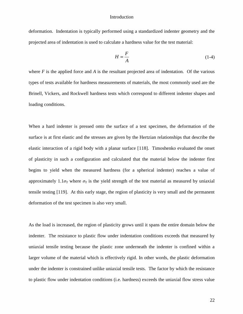
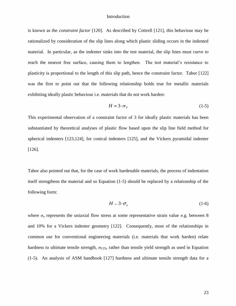
1.3.3 Hardness-Strength Relationships
As described in Section 1.1, the synthesis of bulk quantities of nanomaterials represents a
persistent challenge to researchers. An unfortunate side effect of this inability to produce large
specimens is the reliance on hardness indentation as a means to measure the strength of
nanocrystalline materials. Hardness testing involves indentation of a test material by a rigid
indenter and is therefore a measure of the test material’s resistance to localized plastic
b)
a)
Introduction
22
deformation. Indentation is typically performed using a standardized indenter geometry and the
projected area of indentation is used to calculate a hardness value for the test material:
A
FH (1-4)
where F is the applied force and A is the resultant projected area of indentation. Of the various
types of tests available for hardness measurements of materials, the most commonly used are the
Brinell, Vickers, and Rockwell hardness tests which correspond to different indenter shapes and
loading conditions.
When a hard indenter is pressed onto the surface of a test specimen, the deformation of the
surface is at first elastic and the stresses are given by the Hertzian relationships that describe the
elastic interaction of a rigid body with a planar surface [118]. Timoshenko evaluated the onset
of plasticity in such a configuration and calculated that the material below the indenter first
begins to yield when the measured hardness (for a spherical indenter) reaches a value of
approximately 1.1σY where σY is the yield strength of the test material as measured by uniaxial
tensile testing [119]. At this early stage, the region of plasticity is very small and the permanent
deformation of the test specimen is also very small.
As the load is increased, the region of plasticity grows until it spans the entire domain below the
indenter. The resistance to plastic flow under indentation conditions exceeds that measured by
uniaxial tensile testing because the plastic zone underneath the indenter is confined within a
larger volume of the material which is effectively rigid. In other words, the plastic deformation
under the indenter is constrained unlike uniaxial tensile tests. The factor by which the resistance
to plastic flow under indentation conditions (i.e. hardness) exceeds the uniaxial flow stress value
Introduction
23
is known as the constraint factor [120]. As described by Cottrell [121], this behaviour may be
rationalized by consideration of the slip lines along which plastic sliding occurs in the indented
material. In particular, as the indenter sinks into the test material, the slip lines must curve to
reach the nearest free surface, causing them to lengthen. The test material’s resistance to
plasticity is proportional to the length of this slip path, hence the constraint factor. Tabor [122]
was the first to point out that the following relationship holds true for metallic materials
exhibiting ideally plastic behaviour i.e. materials that do not work harden:
YH 3 (1-5)
This experimental observation of a constraint factor of 3 for ideally plastic materials has been
substantiated by theoretical analyses of plastic flow based upon the slip line field method for
spherical indenters [123,124], for conical indenters [125], and the Vickers pyramidal indenter
[126].
Tabor also pointed out that, for the case of work hardenable materials, the process of indentation
itself strengthens the material and so Equation (1-5) should be replaced by a relationship of the
following form:
oH 3 (1-6)
where σo represents the uniaxial flow stress at some representative strain value e.g. between 8
and 10% for a Vickers indenter geometry [122]. Consequently, most of the relationships in
common use for conventional engineering materials (i.e. materials that work harden) relate
hardness to ultimate tensile strength, σUTS, rather than tensile yield strength as used in Equation
(1-5). An analysis of ASM handbook [127] hardness and ultimate tensile strength data for a
Introduction
24
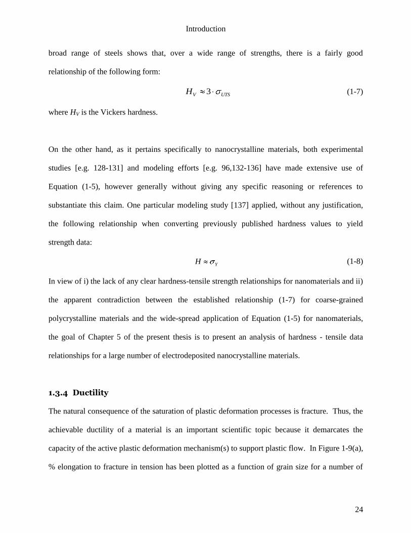
broad range of steels shows that, over a wide range of strengths, there is a fairly good
relationship of the following form:
UTSVH 3 (1-7)
where HV is the Vickers hardness.
On the other hand, as it pertains specifically to nanocrystalline materials, both experimental
studies [e.g. 128-131] and modeling efforts [e.g. 96,132-136] have made extensive use of
Equation (1-5), however generally without giving any specific reasoning or references to
substantiate this claim. One particular modeling study [137] applied, without any justification,
the following relationship when converting previously published hardness values to yield
strength data:
YH (1-8)
In view of i) the lack of any clear hardness-tensile strength relationships for nanomaterials and ii)
the apparent contradiction between the established relationship (1-7) for coarse-grained
polycrystalline materials and the wide-spread application of Equation (1-5) for nanomaterials,
the goal of Chapter 5 of the present thesis is to present an analysis of hardness - tensile data
relationships for a large number of electrodeposited nanocrystalline materials.
1.3.4 Ductility
The natural consequence of the saturation of plastic deformation processes is fracture. Thus, the
achievable ductility of a material is an important scientific topic because it demarcates the
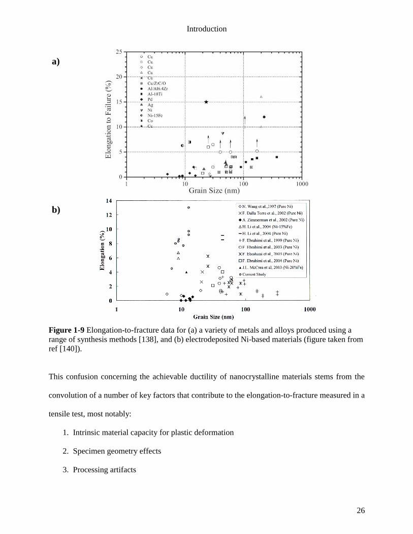
capacity of the active plastic deformation mechanism(s) to support plastic flow. In Figure 1-9(a),
% elongation to fracture in tension has been plotted as a function of grain size for a number of
Introduction
25
different nanocrystalline metals and alloys synthesized using a wide variety of synthesis methods
such as Inert Gas Condensation (IGC), Equal Channel Angular Pressing (ECAP), mechanical
milling, and electrodeposition [138]. None of the measurements were carried out in
conformance with ASTM E8 and many of these materials exhibit approximately 50%
elongation-to-fracture in conventional coarse-grained form. The resultant tensile elongation
values of materials with grain size values below 30nm is in line with those exhibited by
intrinsically brittle materials, with most exhibiting ductility values in the range of 2-3% [139]. It
is not known how much elongation these materials would have exhibited had they been tested
according to the ASTM E8 standardized procedure. There is also a great deal of variability in
the Figure 1-9(a) data, making it difficult to infer whether grain refinement into the
nanocrystalline regime is, in and of itself, the cause of the observations of significantly depressed
ductility.
Even for the subset of nanocrystalline Ni-based materials produced using a single processing
method, namely electrodeposition, the data scatter is immense with some samples having
exhibited greater than 12% elongation-to-fracture in tension while others have exhibited less than
1%, see Figure 1-9(b) [140]. Furthermore, while the measured tensile elongation-to-failure
values were oftentimes low, the associated tensile test fracture surfaces generally exhibited
dimpling indicative of ductile material flow [13,141-143]. Some have deemed the concurrent
observation of fracture surface dimpling (indicative of plasticity) and <1% total macroscopic
elongation-to-fracture (indicative of very little plasticity) a “paradox” in the study of the
mechanical behaviour of nanocrystalline materials [144,145].
Introduction
26
Figure 1-9 Elongation-to-fracture data for (a) a variety of metals and alloys produced using a
range of synthesis methods [138], and (b) electrodeposited Ni-based materials (figure taken from
ref [140]).
This confusion concerning the achievable ductility of nanocrystalline materials stems from the
convolution of a number of key factors that contribute to the elongation-to-fracture measured in a
tensile test, most notably:
1. Intrinsic material capacity for plastic deformation
2. Specimen geometry effects
3. Processing artifacts
a)
b)
Introduction
27
It is therefore an important objective of this work to either eliminate or hold the extrinsic
variables of specimen geometry and processing flaw effects constant in the interest of elucidating
the intrinsic ductility of nanocrystalline materials. The results of that work are contained in
Chapter 4. Beforehand, the goal of section 1.3.4 is to review the current status of nanocrystalline
material ductility with particular emphasis on the influence of the three ductility limiting factors
listed above.
1.3.4.1 Strain Hardening Capacity
In conventional coarse-grained metallic materials, dislocation processes are the dominant carriers
of plastic deformation. Shear stresses acting parallel to the slip plane cause dislocations to move
through the lattice. As dislocations travel, they may encounter obstacles such as solute atoms,
particles, other dislocations, or grain boundaries, effectively impeding their motion until the local
stress is high enough to allow the dislocations to overcome the obstacles. With continued
deformation, the dislocation density increases due to dislocation multiplication and/or the
formation of new dislocations. With this increasing dislocation density, the distance between
them decreases, they encounter each other more often, and it becomes increasingly difficult to
deform the material (as per Equation (1-2)). This process is known as strain or work hardening.
Hollomon’s equation is most commonly used to depict the strain hardening phenomenon. The
Hollomon relationship describes strain hardening as a power law function of true stress and
strain after yielding:
nK (1-9)
Introduction
28
where σ and ε are true stress and strain, n is the strain hardening exponent, and K is the strength
coefficient. n is the measure of the ability of a material to strain harden: the larger its magnitude,
the greater the strain hardening for a given plastic strain. ASTM has provided a standard test
method (ASTM E646) for the measurement of the strain hardening exponent n from tensile
engineering stress-strain data [146].
During the process of plastically deforming a typical metallic tensile specimen, strain hardening
takes place within the material. Concurrently, the gauge cross-sectional area shrinks as the
sample is plastically deformed and the specimen is therefore able to sustain less applied force.
This drop in load bearing capacity due to localized thinning and deformation of the specimen is
known as geometrical softening. Thus, as their names imply, there exists a competition between
strain hardening and geometrical softening as the material is plastically deformed. When the
strain hardening capacity of the material has been saturated, geometrical softening may become
predominate, and plastic flow localization / mechanical instability may occur. In tensile testing,
this takes the form of necking in the gauge section of the specimen. Therefore, in order to
increase the ductility of the material in question, a common strategy is to promote strain
hardening mechanisms since these effectively counteract geometrical softening. In such a
fashion, the onset of tensile instability or necking is delayed as long as possible.
Unfortunately, owing to their small grain size, nanocrystalline materials are believed to possess
little capacity for intracrystalline dislocation interaction which is the traditional basis of strain
hardening in polycrystalline metallic materials. The creation of improved strain hardening
capacity as a means to discourage flow localization in nanocrystalline materials has therefore
Introduction
29
received considerable attention because it offers the potential to achieve an optimum balance
between high strength and good ductility in these materials [e.g. 138]. To this end, the two most
notable strategies that have been employed to date are a) bimodal grain size distributions, and b)
nanotwinning.
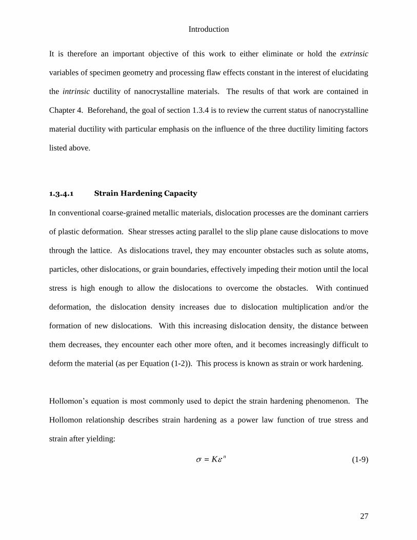
A schematic illustration of the bimodal structure is provided in Figure 1-10(a) [147]. In
principle, if a broad grain size distribution can be synthesized, then it may be possible for the
large grains to provide the strain hardening (related to lattice dislocation accumulation) required
for good ductility while the nanocrystalline matrix contributes high strength and hardness. In
2002, Wang et al. demonstrated this strategy for Cu that was prepared by rolling at liquid
nitrogen temperatures, see curve E in Figure 1-10(b) [148]. The optimal properties (curve E)
were obtained for a material with 1-3µm diameter grains embedded within a matrix of nano- and
submicron-sized grains. The ductility was comparable to that of annealed Cu but the yield
strength was almost seven times higher (curve A in Figure 1-10(b)).
Introduction
30
Figure 1-10 (a) Deformation and fracture processes in a specimen with a bimodal structure
[147], (b) engineering stress–strain curves for pure Cu. Curve A, annealed, coarse grained Cu; B,
room temperature rolling to 95% cold work (CW); C, liquid-nitrogen temperature rolling to 93%
CW; D, 93% CW + 180°C/3 min; and E, 93% CW +200°C/3 min. Note the coexisting high
strength and large uniform plastic strain as well as large overall percentage elongation to failure
for curve E (bimodal structure) [148]; (c) Tensile curves of extruded nanocrystalline Al–7.5Mg
samples with varying concentrations of blended coarse-grained powder to create a bimodal
structure [149].
Lavernia’s group has made numerous important contributions in the synthesis and
characterization of bimodal materials prepared by cryomilling followed by powder compaction
by hot isostatic pressing and extrusion [15,149,150]. For example, Figure 1-10(c) contains
tensile data recorded from cryomilled nanocrystalline Al-7.5%Mg (Al 5083) powder blended
with 15% and 30% of unmilled coarse-grained powder [149]. The addition of larger grains (in
a) b)
c)
Introduction
31
the form of unmilled powder) to the nanocrystalline matrix increased the ductility from
approximately 1.4% to 5.4% elongation while maintaining a strength value approximately four
times higher than conventional Al 5083.
Another technique that may be used to optimize strength and ductility is the formation of
nanotwins, this method having been developed by K. Lu and co-workers [19]. The concept
relies on the fact that twin boundaries impart material strengthening in a fashion similar to
conventional high-angle grain boundaries, namely by blocking dislocation motion. However,
unlike conventional nanocrystalline materials, decreasing the twin lamellae thickness also results
in an increase in work hardening capacity. Apparently the mechanism for this increased work
hardening capacity with increased twin density is that the twin boundaries act as locations for
dislocation accumulation [19,151]. Thus, the structure can be both strong and ductile. Lu and
co-workers have demonstrated that Cu with a grain size of 400-500nm and twin lamellae
thicknesses in the range of 20-100nm provide adequate barriers to dislocation motion for
strengthening while creating local sites for nucleating and accommodating dislocations, thereby
elevating ductility and work hardening [19]. Characterization data from this structure is
provided in Figure 1-11.
Introduction
32
Figure 1-11 (top) Transmission electron microscopy (TEM) observations of the typical
microstructure in an as-deposited nanotwinned Cu sample. A bright field TEM image (A) and
the electron diffraction pattern (inset in (A)) show roughly equiaxed submicron-sized grains with
random orientations separated by high angle grain boundaries; (bottom) a typical tensile stress-
strain curve for the Cu sample with nano-twins in comparison with that for a coarse-grained
polycrystalline Cu (average grain size >100 µm) and a nanocrystalline Cu sample (mean grain
size ~ 30 nm) [19].
Hence, enhanced strain hardening represents a powerful tool with which the onset of mechanical
instability in tension may be delayed. Such work requires modification of the microstructure of
the material, which is beyond the scope of the present study. Rather, this study was focused
primarily on the effects of processing artifacts and specimen geometry on achievable ductility in
nanomaterials possessing fairly narrow grain size distributions, these factors having been largely
overlooked in the field.
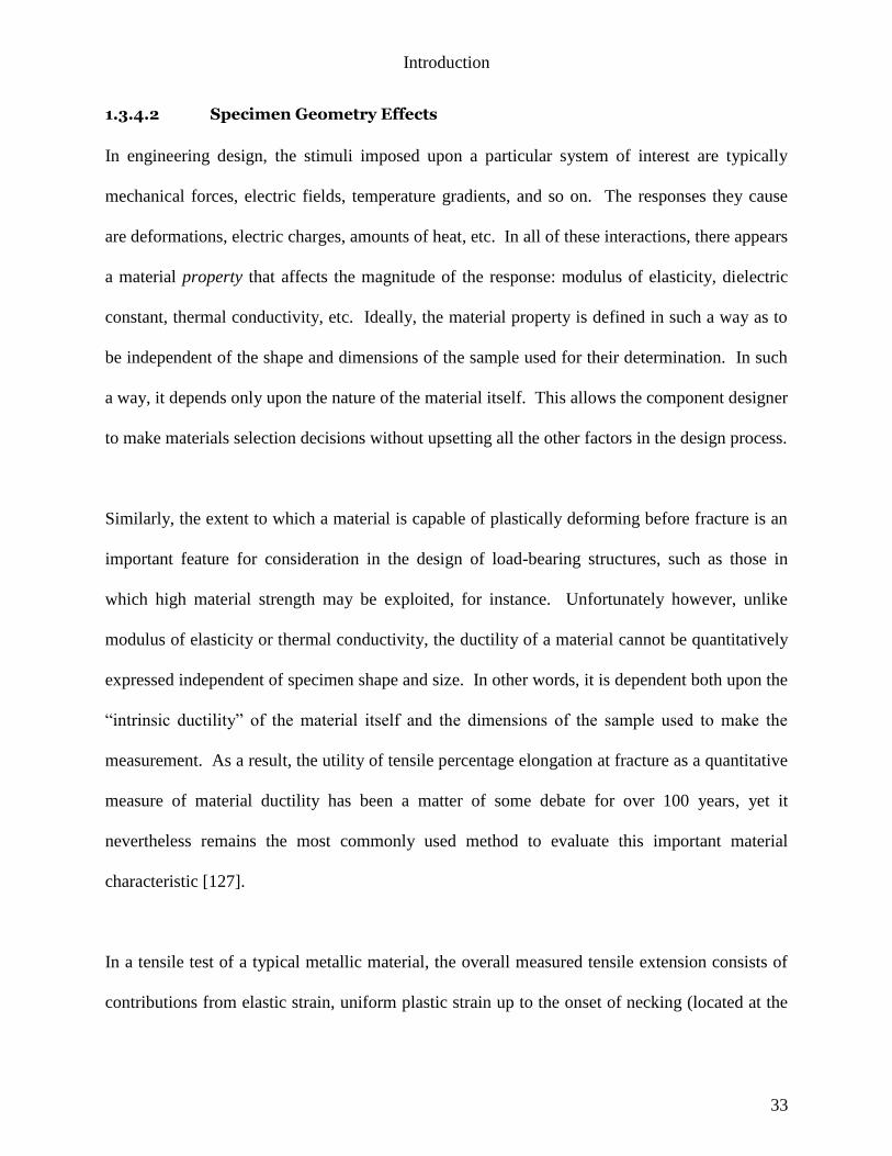
Introduction
33
1.3.4.2 Specimen Geometry Effects
In engineering design, the stimuli imposed upon a particular system of interest are typically
mechanical forces, electric fields, temperature gradients, and so on. The responses they cause
are deformations, electric charges, amounts of heat, etc. In all of these interactions, there appears
a material property that affects the magnitude of the response: modulus of elasticity, dielectric
constant, thermal conductivity, etc. Ideally, the material property is defined in such a way as to
be independent of the shape and dimensions of the sample used for their determination. In such
a way, it depends only upon the nature of the material itself. This allows the component designer
to make materials selection decisions without upsetting all the other factors in the design process.
Similarly, the extent to which a material is capable of plastically deforming before fracture is an
important feature for consideration in the design of load-bearing structures, such as those in
which high material strength may be exploited, for instance. Unfortunately however, unlike
modulus of elasticity or thermal conductivity, the ductility of a material cannot be quantitatively
expressed independent of specimen shape and size. In other words, it is dependent both upon the
“intrinsic ductility” of the material itself and the dimensions of the sample used to make the
measurement. As a result, the utility of tensile percentage elongation at fracture as a quantitative
measure of material ductility has been a matter of some debate for over 100 years, yet it
nevertheless remains the most commonly used method to evaluate this important material
characteristic [127].
In a tensile test of a typical metallic material, the overall measured tensile extension consists of
contributions from elastic strain, uniform plastic strain up to the onset of necking (located at the
Introduction
34
point on the stress-strain curve commonly known as the “ultimate tensile stress”, point M in
Figure 1-12), and the localized or non-uniform plastic strain after the onset of necking until final
fracture (strain between points M and F in Figure 1-12).
Figure 1-12 Typical engineering stress-strain behaviour to fracture, point F. The “ultimate
tensile strength” is indicated at point M. The circular insets represent the geometry of the
deformed specimen at various points along the curve [61].
As discussed in section 1.3.4.1, the extent of uniform elongation that is achievable is dictated
primarily by the work hardening capacity of the material. However, the measured elongation-to-
fracture also typically includes a contribution from non-uniform strain arising from localized
deformation of the specimen after the onset of necking. In particular, there is a strong
dependency of achievable post-uniform linear strain on sample size and shape because these
geometrical factors play a key role in the process of neck formation during tensile extension. In
general, for metallic specimens of similar geometry in terms of dimensional proportionality
(ratios of specimen width to length to thickness and so on), the larger the specimen gauge cross-
sectional area, the more necking the sample is able to sustain before fracture. Hence, a sample
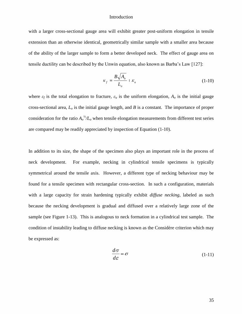
Introduction
35
with a larger cross-sectional gauge area will exhibit greater post-uniform elongation in tensile
extension than an otherwise identical, geometrically similar sample with a smaller area because
of the ability of the larger sample to form a better developed neck. The effect of gauge area on
tensile ductility can be described by the Unwin equation, also known as Barba’s Law [127]:
u
o
o
fL
AB (1-10)
where εf is the total elongation to fracture, εu is the uniform elongation, Ao is the initial gauge
cross-sectional area, Lo is the initial gauge length, and B is a constant. The importance of proper
consideration for the ratio Ao½/Lo when tensile elongation measurements from different test series
are compared may be readily appreciated by inspection of Equation (1-10).
In addition to its size, the shape of the specimen also plays an important role in the process of
neck development. For example, necking in cylindrical tensile specimens is typically
symmetrical around the tensile axis. However, a different type of necking behaviour may be
found for a tensile specimen with rectangular cross-section. In such a configuration, materials
with a large capacity for strain hardening typically exhibit diffuse necking, labeled as such
because the necking development is gradual and diffused over a relatively large zone of the
sample (see Figure 1-13). This is analogous to neck formation in a cylindrical test sample. The
condition of instability leading to diffuse necking is known as the Considère criterion which may
be expressed as:
d
d (1-11)
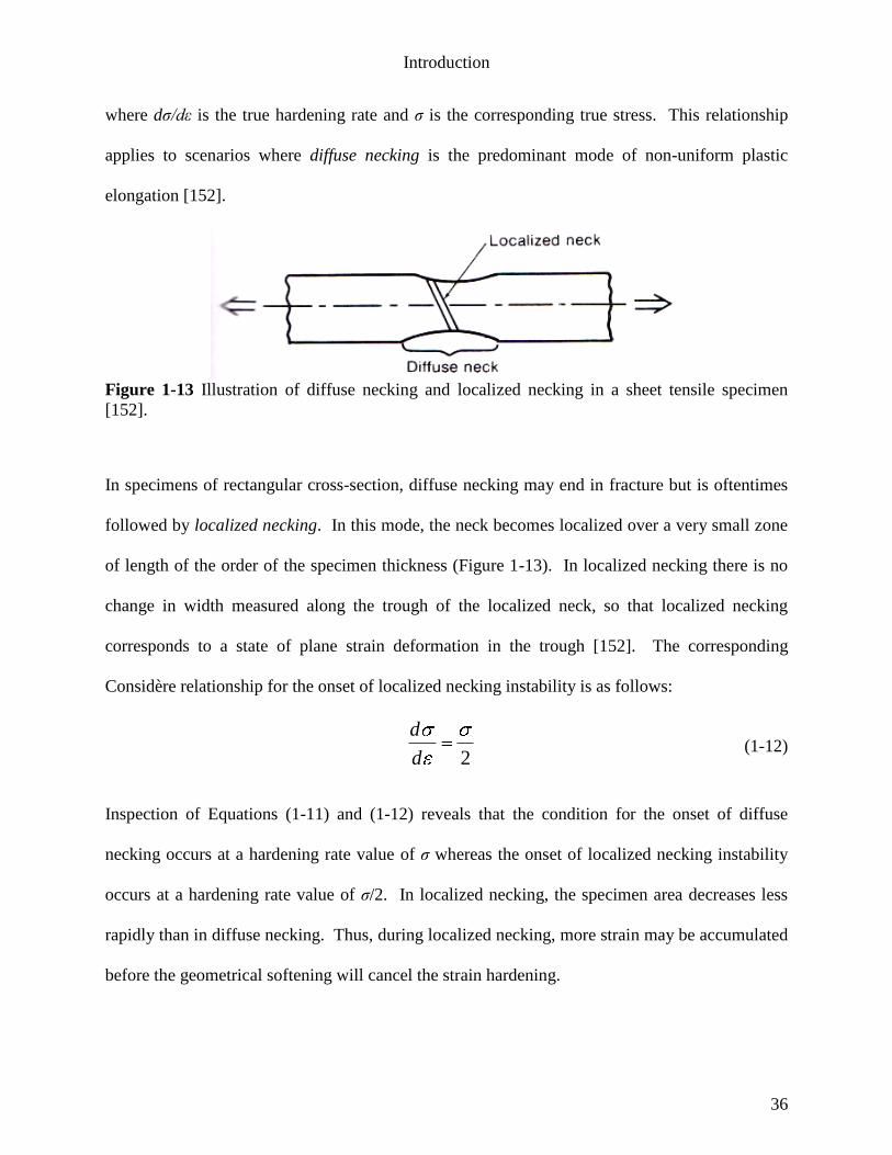
Introduction
36
where dσ/dε is the true hardening rate and σ is the corresponding true stress. This relationship
applies to scenarios where diffuse necking is the predominant mode of non-uniform plastic
elongation [152].
Figure 1-13 Illustration of diffuse necking and localized necking in a sheet tensile specimen
[152].
In specimens of rectangular cross-section, diffuse necking may end in fracture but is oftentimes
followed by localized necking. In this mode, the neck becomes localized over a very small zone
of length of the order of the specimen thickness (Figure 1-13). In localized necking there is no
change in width measured along the trough of the localized neck, so that localized necking
corresponds to a state of plane strain deformation in the trough [152]. The corresponding
Considère relationship for the onset of localized necking instability is as follows:
2d
d (1-12)
Inspection of Equations (1-11) and (1-12) reveals that the condition for the onset of diffuse
necking occurs at a hardening rate value of σ whereas the onset of localized necking instability
occurs at a hardening rate value of σ/2. In localized necking, the specimen area decreases less
rapidly than in diffuse necking. Thus, during localized necking, more strain may be accumulated
before the geometrical softening will cancel the strain hardening.
Introduction
37
Furthermore, in materials with little strain hardening capacity (e.g. cold rolled strip) the
condition of instability, and hence the strain at both diffuse and localized necking, may both
approach zero strain. Specimens of rectangular cross-section cut from material with little strain
hardening capacity may therefore exhibit a distinct localized necking mode before fracture.
Another prominent feature of localized necking is the oblique fracture angle of approximately
55° relative to the loading axis. The tendency for wide bars of strain hardened metals to fracture
in this manner was first recognized by Koerber and Siebel in 1928 [153], and Bijlaard
subsequently provided a first principles calculation of the 55° angle based upon principal stresses
[154]. Further commentary on the plastic instability of wide flat tensile specimens and the 55°
angle may be found in [155,156]. Figure 1-14 contains photographs of cold rolled Al and steel
sheet illustrating the predominant localized necking mode and oblique 55° fracture.
Figure 1-14 Photographs of the gauge sections of fractured tensile test coupons from (a) cold
rolled steel [155], and (b) cold rolled Al [157], illustrating localized necking and the 55° fracture
angle.
a) b)
Introduction
38
To address the ductility sensitivity to sample geometry, materials scientists and engineers have
established standardized protocols for the measurement of ductility wherein mechanical test
specimen dimensions are prescribed for common use. In this manner, ductility data from one
material may be systematically recorded and compared to data gathered from another material.
One widely used test specification is ASTM E8 [11], which provides a guideline for the tension
test, the most commonly accepted method of measuring ductility. Unfortunately, the ASTM
standard test geometries are much larger and thicker than the thin sheets or small coupons of
feedstock nanocrystalline materials that have been synthesized by or made available to most
researchers in the field. For illustrative purposes, Figure 1-15 contains schematic drawings of
some of the tensile sample geometries found in the electrodeposited nanomaterials literature
alongside the ASTM standard subsize tensile coupon geometry [11] and that used in the current
study. Interestingly, the smallest sample geometry in Figure 1-15, of 3mm in total length, was
heavily used in one of the most cited papers on the topic, namely the work of Dalla Torre et al.
[13]. See Figure 1-2(b) for a photograph of these specimens. Upon examination of Figure 1-15
in conjunction with Equation (1-10), it may be readily appreciated that ductility measurements
recorded using miniature samples may be unsuitable for comparison to those of other well-
known engineering metallic materials characterized in conformance with the standard ASTM
specification. On the other hand, note that the gauge section of the specimens for the current
study is identical to that of ASTM E8, the only notable difference being the tab width which was
widened to provide increased gripping area after slipping problems owing to the extremely high
material strength were experienced. The sensitivity of electrodeposited nanocrystalline material
ductility to specimen geometry is explored in Chapter 4.
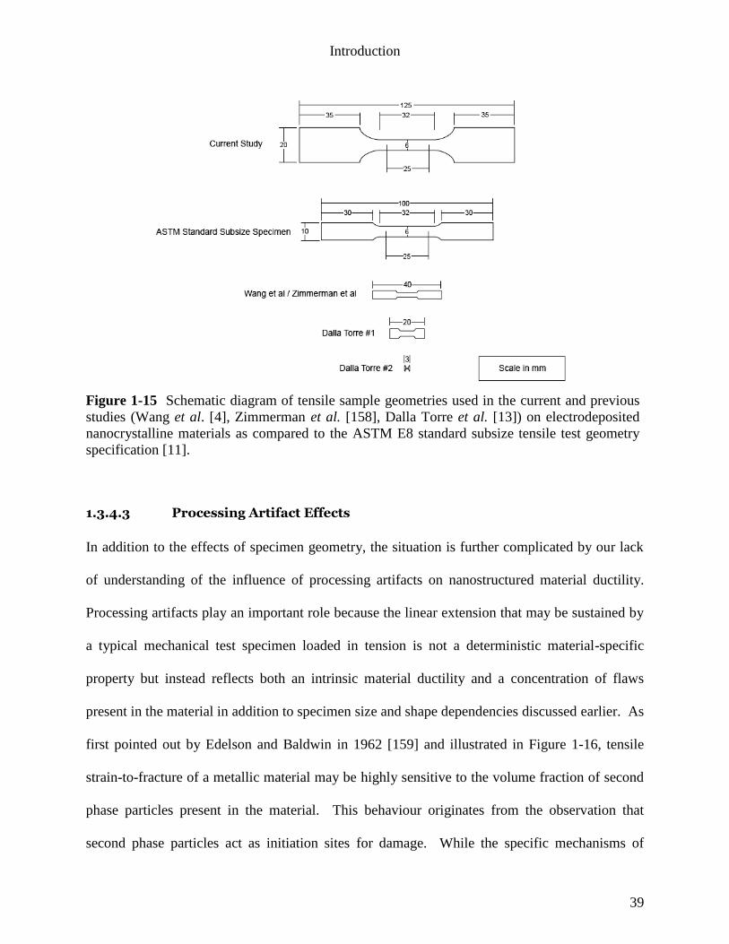
Introduction
39
1.3.4.3 Processing Artifact Effects
In addition to the effects of specimen geometry, the situation is further complicated by our lack
of understanding of the influence of processing artifacts on nanostructured material ductility.
Processing artifacts play an important role because the linear extension that may be sustained by
a typical mechanical test specimen loaded in tension is not a deterministic material-specific
property but instead reflects both an intrinsic material ductility and a concentration of flaws
present in the material in addition to specimen size and shape dependencies discussed earlier. As
first pointed out by Edelson and Baldwin in 1962 [159] and illustrated in Figure 1-16, tensile
strain-to-fracture of a metallic material may be highly sensitive to the volume fraction of second
phase particles present in the material. This behaviour originates from the observation that
second phase particles act as initiation sites for damage. While the specific mechanisms of
Figure 1-15 Schematic diagram of tensile sample geometries used in the current and previous
studies (Wang et al. [4], Zimmerman et al. [158], Dalla Torre et al. [13]) on electrodeposited
nanocrystalline materials as compared to the ASTM E8 standard subsize tensile test geometry
specification [11].
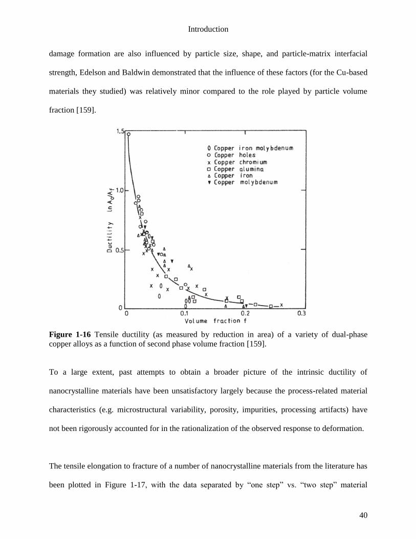
Introduction
40
damage formation are also influenced by particle size, shape, and particle-matrix interfacial
strength, Edelson and Baldwin demonstrated that the influence of these factors (for the Cu-based
materials they studied) was relatively minor compared to the role played by particle volume
fraction [159].
Figure 1-16 Tensile ductility (as measured by reduction in area) of a variety of dual-phase
copper alloys as a function of second phase volume fraction [159].
To a large extent, past attempts to obtain a broader picture of the intrinsic ductility of
nanocrystalline materials have been unsatisfactory largely because the process-related material
characteristics (e.g. microstructural variability, porosity, impurities, processing artifacts) have
not been rigorously accounted for in the rationalization of the observed response to deformation.
The tensile elongation to fracture of a number of nanocrystalline materials from the literature has
been plotted in Figure 1-17, with the data separated by “one step” vs. “two step” material
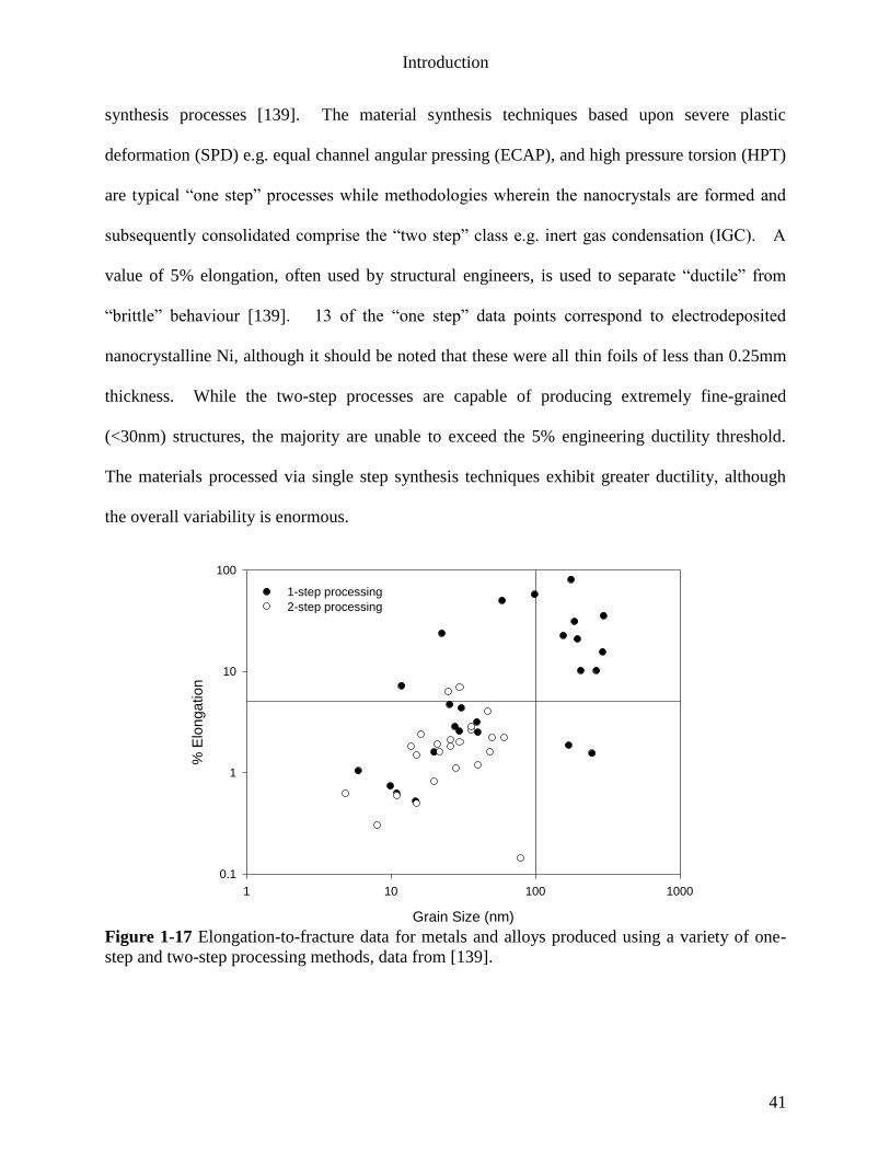
Introduction
41
synthesis processes [139]. The material synthesis techniques based upon severe plastic
deformation (SPD) e.g. equal channel angular pressing (ECAP), and high pressure torsion (HPT)
are typical “one step” processes while methodologies wherein the nanocrystals are formed and
subsequently consolidated comprise the “two step” class e.g. inert gas condensation (IGC). A
value of 5% elongation, often used by structural engineers, is used to separate “ductile” from
“brittle” behaviour [139]. 13 of the “one step” data points correspond to electrodeposited
nanocrystalline Ni, although it should be noted that these were all thin foils of less than 0.25mm
thickness. While the two-step processes are capable of producing extremely fine-grained
(<30nm) structures, the majority are unable to exceed the 5% engineering ductility threshold.
The materials processed via single step synthesis techniques exhibit greater ductility, although
the overall variability is enormous.
Grain Size (nm)
1 10 100 1000
% E
lon
ga
tio
n
0.1
1
10
100
1-step processing
2-step processing
Figure 1-17 Elongation-to-fracture data for metals and alloys produced using a variety of one-
step and two-step processing methods, data from [139].
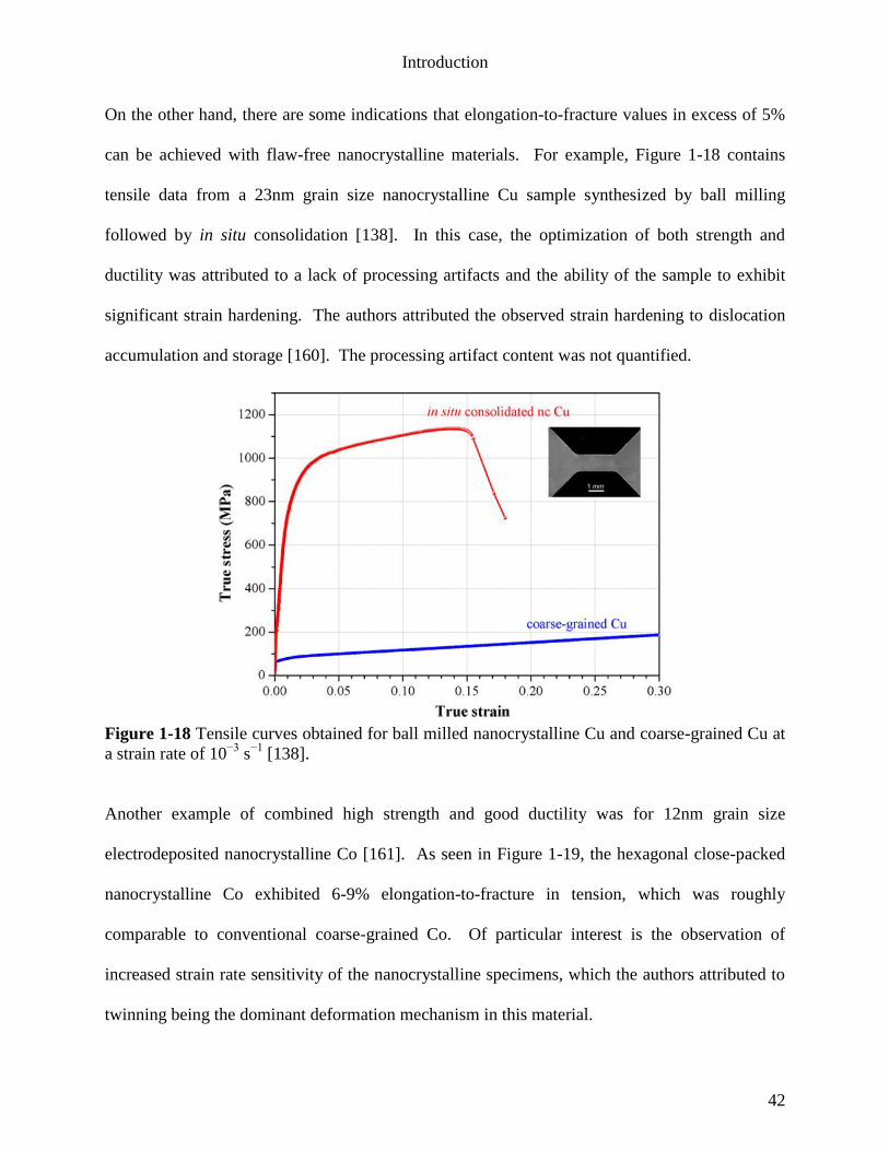
Introduction
42
On the other hand, there are some indications that elongation-to-fracture values in excess of 5%
can be achieved with flaw-free nanocrystalline materials. For example, Figure 1-18 contains
tensile data from a 23nm grain size nanocrystalline Cu sample synthesized by ball milling
followed by in situ consolidation [138]. In this case, the optimization of both strength and
ductility was attributed to a lack of processing artifacts and the ability of the sample to exhibit
significant strain hardening. The authors attributed the observed strain hardening to dislocation
accumulation and storage [160]. The processing artifact content was not quantified.
Figure 1-18 Tensile curves obtained for ball milled nanocrystalline Cu and coarse-grained Cu at
a strain rate of 10−3
s−1
[138].
Another example of combined high strength and good ductility was for 12nm grain size
electrodeposited nanocrystalline Co [161]. As seen in Figure 1-19, the hexagonal close-packed
nanocrystalline Co exhibited 6-9% elongation-to-fracture in tension, which was roughly
comparable to conventional coarse-grained Co. Of particular interest is the observation of
increased strain rate sensitivity of the nanocrystalline specimens, which the authors attributed to
twinning being the dominant deformation mechanism in this material.
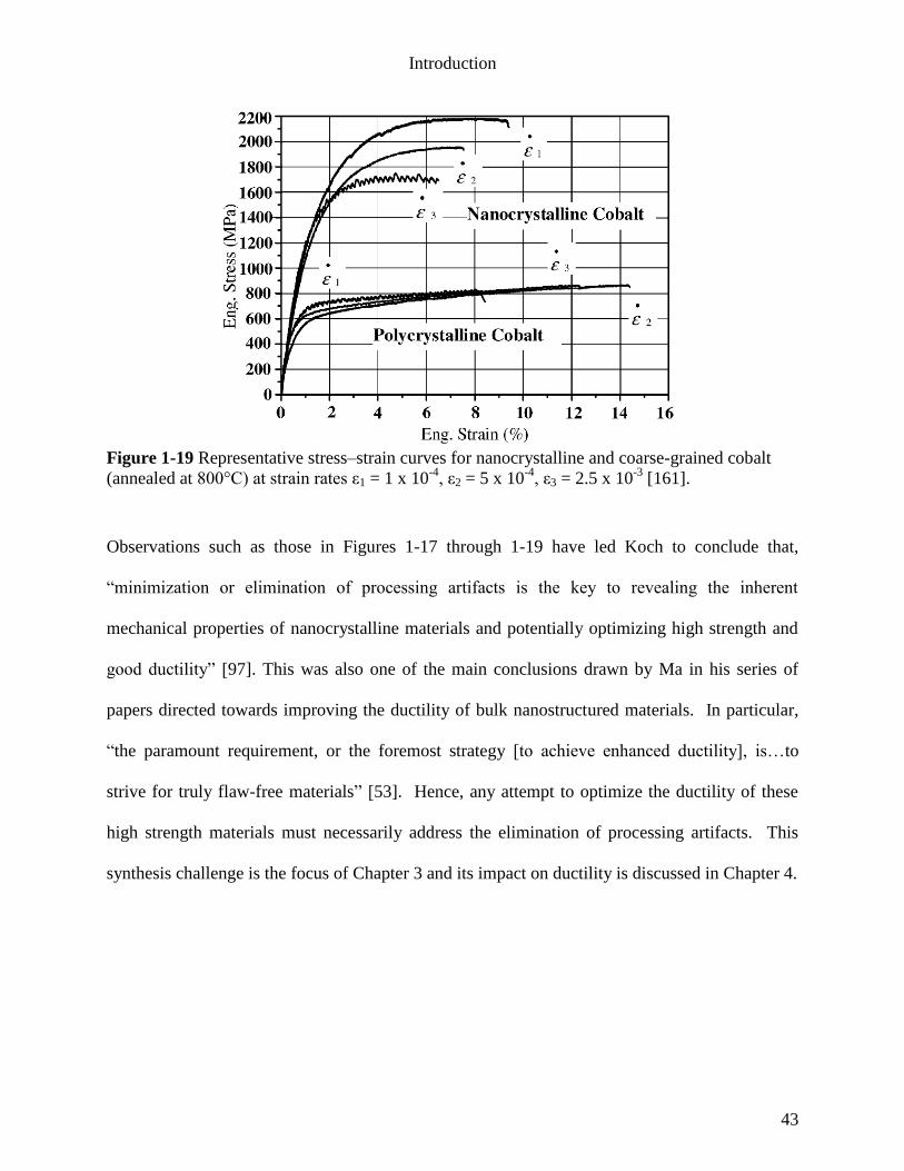
Introduction
43
Figure 1-19 Representative stress–strain curves for nanocrystalline and coarse-grained cobalt
(annealed at 800°C) at strain rates ε1 = 1 x 10⁻⁴
, ε2 = 5 x 10⁻⁴
, ε3 = 2.5 x 10⁻³
[161].
Observations such as those in Figures 1-17 through 1-19 have led Koch to conclude that,
“minimization or elimination of processing artifacts is the key to revealing the inherent
mechanical properties of nanocrystalline materials and potentially optimizing high strength and
good ductility” [97]. This was also one of the main conclusions drawn by Ma in his series of
papers directed towards improving the ductility of bulk nanostructured materials. In particular,
“the paramount requirement, or the foremost strategy [to achieve enhanced ductility], is…to
strive for truly flaw-free materials” [53]. Hence, any attempt to optimize the ductility of these
high strength materials must necessarily address the elimination of processing artifacts. This
synthesis challenge is the focus of Chapter 3 and its impact on ductility is discussed in Chapter 4.
Introduction
44
1.3.4.4 Closing Remarks on Nanocrystalline Material Ductility
In conclusion, it may be readily appreciated that, in addition to specimen geometry effects, the
fact that nanocrystalline materials can be created using a wide variety of fundamentally
dissimilar processing techniques that result in tremendously varying microstructures and
processing artifacts has hindered the development of our understanding of the intrinsic ductility
of this important material class. A strong emphasis has been placed on improving ductility by
structural control (bimodal structures, twin formation, etc) whereas relatively little headway has
been made in eliminating processing artifacts, arguably a more critical contributor. In addition,
while plastic flow instability is influenced by microstructure (competition between strain
hardening and geometric softening), it is also sensitive to specimen geometry (as will be
demonstrated in Chapter 4). Again, this has received little attention in the community.
Therefore, as it relates to material ductility, a focused study to elucidate the effects of
electroforming processing artifacts and specimen geometry on nanocrystalline material ductility
is required. It is therefore an important objective of this work to produce a very large number of
bulk samples synthesized from a gross artifact-reduced, steady state electroforming process, test
them in conformance with ASTM E8, and then quantify the distributional variability in intrinsic
ductility of the materials using Weibull distributional analysis.
Introduction
45
1.4 Research Objectives
Objective #1
As described in Section 1.3, a great deal of work has been devoted to the study of nanocrystalline
materials and their mechanical properties. However, some of the most important mechanical
properties (most notably ductility and elastic modulus) are known to be highly sensitive to the
presence of processing artifacts. It is therefore the first objective of this work to synthesize
artifact-reduced nanocrystalline materials. This is addressed in Chapter 3.
Objective #2
An inability to produce bulk quantities of nanocrystalline materials has prevented tensile testing
according to standardized test protocols such as ASTM E8. The persistent use of non-
standardized specimen geometries has resulted in considerable confusion concerning the intrinsic
mechanical properties of nanocrystalline materials. It is therefore the second objective of this
study to synthesize bulk quantities of electroformed nanocrystalline materials suitable for
testing in conformance with ASTM E8. This work is also presented in Chapter 3.
Objective #3
With bulk quantities of artifact-reduced feedstock material in-hand, tensile testing in
conformance with ASTM E8 was then performed. The specific focus of Chapter 4 is ductility,
including an examination of the influence of processing artifacts and specimen size and
shape on the achievable tensile elongation of nanocrystalline materials.
Introduction
46
Objective #4
Because the linear extension that may be sustained by a typical mechanical test specimen loaded
in tension is not a deterministic material-specific property but instead reflects a distribution (size
and orientation) of flaws present in the material in addition to the intrinsic material ductility and
specimen size and shape dependencies, a thorough analysis of nanocrystalline material ductility
requires a statistically significant set of specimens. In particular, the fourth objective is the
synthesis of a large number of samples to enable a statistical evaluation of achievable
ductility by Weibull distributional analysis. This is presented in Chapter 4.
Objective #5
The inability to synthesize bulk quantities of nanocrystalline material has forced many
researchers to rely on hardness indentation as a proxy for strength. Unfortunately, there has been
little consensus concerning which hardness-strength relationships can or should be applied, and
this has resulted in misleading information concerning the intrinsic strength of nanocrystalline
materials. Hence, it is the objective of Chapter 5 to elucidate those conditions under which
hardness may be reliably used to evaluate the strength of electrodeposited nanocrystalline
materials.
Introduction
47
1.5 References
[1] E.O. Hall, Proc. Phys. Soc., Lond. B 64 (1951) 747.
[2] N.J. Petch, J. Iron Steel Inst., Lond. 173 (1953) 25.
[3] L.S. Darken, Trans. Amer. Soc. Met. 54 (1961) 600.
[4] N. Wang, Z. Wang, K.T. Aust, U. Erb, Acta Metall. Mater. 43, 2 (1995) 519.
[5] H. Gleiter, Proc. 2nd
Int. Symp. Metall. And Mater. Sci., Risø National Laboratory, Roskilde,
Denmark (1981) 15.
[6] H. Gleiter, Prog. Mat. Sci., 33 (1989) 223..
[7] A.H. Chokshi, A. Rosen, J. Karch, H. Gleiter, Scripta Mater., 25 (1989) 641.
[8] A.M. El-Sherik, U. Erb, G. Palumbo, K.T. Aust, Scripta Metall. Mater., 27 (1992) 1185.
[9] C.C. Koch, J. Narayan, MRS Symp. Proc. Vol. 634, eds. D. Farkas, H. Kung, M. Mayo, H.
Van Swygenhoven, J.R. Weertman, MRS, Warrendale, PA (2001) B5.1.1.
[10] G. Saada, Phil. Mag. 85, 26-27 (2005) 3003.
[11] ASTM Standard E8/E8M-09, ASTM International, West Conshohocken, PA (2009).
[12] M. Legros, B.R. Elliott, M.N. Rittner, J.R. Weertman, K.J. Hemker, Phil. Mag. A, 80, 4
(2000) 1017.
[13] F. Dalla Torre, H. Van Swygenhoven, M. Victoria, Acta Mater. 50 (2002) 3957.
[14] C.C. Koch, R.O. Scattergood, K.M. Youssef, E. Chan, Y.T. Zhu, J. Mater. Sci. 45 (2010)
4725.
[15] D.B. Witkin, E.J. Lavernia, Prog. Mater. Sci. 51 (2006) 1.
[16] V. Krstic, U. Erb, G. Palumbo, Scripta Metall. et Mater. 29 (1993) 1501.
[17] R.Z. Valiev, T.G. Langdon, Prog. Mater. Sci. 51 (2006) 881.
[18] G. Herzer, J. Magn. Magn. Mater. 112,1-3 (1992) 258.
Introduction
48
[19] L. Lu, Y. Shen, X. Chen, L. Qian, K Lu, Science 304 (2004) 422.
[20] J. Luo, Z. Mei, W. Tian, Z. Wang, Mat. Sci. Eng. A 441 (2006) 282.
[21] X.H. Chen, L. Lu, K Lu, Scripta Mater. 64 (2011) 311.
[22] C.C. Koch (ed.), Nanostructured Materials: Processing, Properties and Applications, 1st ed.,
Noyes Pub. / William Andrew Pub., Norwich, NY (2002)
[23] C.C. Koch (ed.), Nanostructured Materials: Processing, Properties and Applications, 2nd
ed.,
William Andrew Pub., Norwich, NY (2007).
[24] C.C. Koch, I.A. Ovid’ko, S. Seal, S. Veprek, Structural Nanocrystalline Materials:
Fundamentals and Applications, Cambridge University Press, Cambridge, UK (2007).
[25] S.H. Whang (ed.), Nanostructured Metals and Alloys: Processing, Microstructure,
Mechanical Properties and Applications, Woodhead Pub., Cambridge, UK (2011).
[26] M.Y. Gutkin, I.A. Ovid’ko, Plastic Deformation in Nanocrystalline Materials, Springer
(2004).
[27] G.M. Chow, I.A. Ovid’ko, T. Tsakalakos (eds.), Nanostructured Films and Coatings, NATO
Science Series, Kluwer Pub. (1999).
[28] C. Suryanarayana, J. Singh, F.H. Froes (eds.), Processing and Properties of Nanocrystalline
Materials, TMS, Warrendale, PA (1995).
[29] M.J. Yacaman, T. Tsakalakos, B.H. Kear (eds.), Proceedings of the First International
Conference on Nanostructured Materials, Nanostr. Mater. 3, 1-6 (1993) 1.
[30] M.J. Yacaman, T. Tsakalakos, B.H. Kear (eds.), Proceedings of the Second International
Conference on Nanostructured Materials, Nanostr. Mater. 6, 1-8 (1995) 1.
[31] M.L. Trudeau, V. Provenzano, R.D. Schull, J.Y. Ying (eds.), Proceedings of the Third
International Conference on Nanostructured Materials, Nanostr. Mater. 9, 1-8 (1997) 1.
Introduction
49
[32] M. Muhammed, K.V. Rao (eds.), Proceedings of the Fourth International Conference on
Nanostructured Materials, Nanostr. Mater. 12, 1-8 (1999) 1.
[33] A. Inoue, K. Niihara, R.D. Schull, E. Matsubara (eds.), Proceedings of the Fifth
International Conference on Nanostructured Materials, Scripta Mater. 44, 8 (2001) 1161.
[34] R.Z. Valiev, T.G. Langdon, I.V. Alexandrov, Y.T. Zhu, Y. Estrin, G. Kostorz (eds.),
International Symposium on Bulk Nanostructured Materials: from Fundamentals to Innovation,
BNM 2007, Mater. Sci. Eng. A 503, 1-2 (2009) 1.
[35] X. Zhang, G. Kostorz, C.T. Liu, J.M. Rigsbee, C. Suryanarayana, H. Wang, Y.T. Zhu, D.
Zhang (eds.), Mechanical Behavior of Nanostructured Materials, a Symposium Held in Honor of
Carl Koch at the TMS Annual Meeting 2007, Orlando, Florida, Mater. Sci. Eng. A 493, 1-2
(2008) 1.
[36] H. Van Swygenhoven, J.R. Weertman (eds.), Viewpoint Set No. 31, Mechanical Properties
of Fully Dense Nanocrystalline Metals, Scripta Mater., 49 (1993) 625.
[37] Y.T. Zhu, Z.L. Wang, T.G. Langdon (eds.), Nanostructured Materials – Processing,
Structures, Properties and Applications, J. Mater. Sci. 42, 5 (2007).
[38] X. Huang (ed.), Viewpoint Set No. 45, Nanostructured metals: Advances in Processing,
Characterization and Applications, Scripta Mater., 60, 12 (2009) 1031.
[39] H. Gleiter, Acta Mater. 48 (2000) 1.
[40] M. Yu. Gutkin. I.A. Ovid’ko, C.S. Pande, Rev. Adv. Mater. Sci. 2(2001) 80.
[41] F.A. Mohammed, Y. Li, Mater. Sci. Eng. A 298 (2001) 1.
[42] K.A. Padmanabhan, Mater. Sci. Eng. A 304-306 (2001) 200.
[43] A.K. Mukherjee, Mater. Sci. Eng. A 322 (2002) 1.
[44] M. Yu. Gutkin, I.A. Ovid’ko, Rev. Adv. Mater. Sci. 4 (2003) 79.
Introduction
50
[45] K.S. Kumar, H. Van Swygenhoven, S. Suresh, Acta Mater. 51 (2003) 5743.
[46] S.C. Tjong, H. Chen, Mater. Sci. Eng. R 45 (2004) 1.
[47] R.J. Asaro, S. Suresh, Acta Mater. 53 (2005) 3369.
[48] B.Q. Han, E.J. Lavernia, F.A. Mohammed, Rev. Adv. Mater. Sci. 9 (2005) 1.
[49] J. Weismueller, J. Markmann, Adv. Eng. Mater. 7,4 (2005) 202.
[50] I.A. Ovid’ko, Int. Mater. Rev. 50 (2005) 65.
[51] I.A. Ovid’ko, Rev. Adv. Mater. Sci. 10 (2005) 89.
[52] D. Wolf, V. Yamakov, S.R. Philpot, A. Mukherjee, H. Gleiter, Acta Mater. 53 (2005) 1.
[53] E. Ma, JOM 58 (2006) 49.
[54] M.A. Meyers, A. Mishra, D.J. Benson, Prog. Mater. Sci. 51 (2006) 427.
[55] H. Van Swygenhoven, J.R. Weertman, Mater. Today, 9,5 (2006) 24.
[56] F.H. Dalla Torre, A.A. Gazder, E.V. Pereloma, C.H.J. Davies, J. Mater. Sci. 42 (2007)
1622.
[57] M. Dao, L. Lu, R.J. Asaro, J.T.M. De Hosson, E. Ma, Acta Mater. 55 (2007) 4041.
[58] H. Van Swygenhoven, Mater. Sci. Eng. A 483-484 (2008) 33.
[59] A.P. Zhilyaev, T.G. Langdon, Prog. Mater. Sci. 53 (2008) 893.
[60] C.S. Pande, K.P. Cooper, Prog. Mater. Sci. 54 (2009) 689.
[61] W.D. Callister Jr, Materials Science and Engineering – An Introduction, sixth ed., John
Wiley, New York, NY (2003) 112.
[62] D. Wolf, in Materials Interfaces: Atomic-Level Structure and Properties, D. Wolf, S. Yip
(eds.), Chapman and Hall, London, UK (1992).
[63] D. Wolf, Phil. Mag. B, 59 (1989) 667.
[64] D. Korn, A. Morsch, R. Birringer, W. Arnold, H. Gleiter, J. de Phys., Coll. C5,
Introduction
51
Suppl. Au no. 10, 49 (1988) C5-769.
[65] G.W. Nieman, J.R. Weertman, R.W. Siegel, Scripta Metall., 24 (1990) 145.
[66] G.W. Nieman, J.R. Weertman, R.W. Siegel, J. Mater. Res., 6 (1991) 1012.
[67] M.J. Mayo, R.W. Siegel, Y.X. Liao, W.D. Nix, J. Mater. Res., 7 (1992) 973.
[68] M.J. Mayo, R.W. Siegel, A. Narayanasamy, W.D. Nix, J. Mater. Res., 5 (1990) 1073.
[69] N.P. Kobelev, Y.M. Soifer, R.A. Andrievski, B. Gunther, Nanostr. Mater., 2 (1993) 537.
[70] M. Weller, J. Diehl, H.E. Schaefer, Phil. Mag., A, 63 (1991) 527.
[71] L. Wong, D. Ostrander, U. Erb, G. Palumbo, K.T. Aust, Proc. Symp. on
Nanophases and Nanocrystalline Structures, R.D. Schull, J.M. Sanchez (eds.),
AIME, 85 (1994).
[72] G.E. Fougere, L. Riester, M. Ferber, J.R. Weertman, R.W. Siegel, Mater. Sci.
Eng., A204 (1995) 1.
[73] A.R. Boccaccini, G. Ondracek, P. Mazilu, D. Windelberg, J. Mech. Behav. Mater.,
4 (1993) 119.
[74] H.S. Kim, M.B. Bush, Nanostr. Mater., 11 (1999) 3.
[75] B. Budiansky, J. Composite Mater., 4 (1970) 286.
[76] T.D. Shen, C.C. Koch, T.Y. Tsui, G.M. Pharr, J. Mater. Res., 10 (1995) 2892.
[77] R.Z. Valiev, A.V. Kornikov, R.R. Mulyukov, Mater. Sci. Eng., A168 (1993) 141.
[78] S.R. Agnew, J.R. Weertman, Mater. Sci. Eng., A242 (1998) 174.
[79] Y. Zhou, U. Erb, K.T. Aust, G. Palumbo, Z. Metallkd., 94, 10 (2003) 1.
[80] J.R. Weertman, D. Farkas, K. Hemker, H. Kung, M. Mayo, R. Mitra, H. Van
Swygenhoven, MRS Bull., 44 (Feb. 1999).
[81] H. Van Swygenhoven, A. Caro, Nanophase and Nanocomposite Mater. II, MRS
Introduction
52
Symp. Proc., 457 (1997) 193.
[82] J. Schiotz, T. Vegge, F.D. Di Tolla, K.W. Jacobsen, Modelling of Structure and
Mechanics of Materials from Microscale to Product, J.V. Carstensen et al. (eds.), Risφ
National Laboratory, Denmark, (1998) 133.
[83] R.E. Reed-Hill, R. Abbaschian, Physical Metallurgy Principles, third ed., PWS Pub.,
Boston, MA (1994) 159.
[84] G.S. Was, T. Foecke, Thin Sol. Films, 286 (1996) 1.
[85] W. Wang, R.N. Singh, Mat. Sci. Eng. A 271 (1999) 306.
[86] A. Misra, H. Kung, Adv. Eng. Mater., 3 (2001) 217.
[87] Y.F. Shen, L. Lu, Q.H. Lu, Z.H. Jin, K. Lu, Scripta Mater. 52 (2005) 989.
[88] L.P. Evers, D.M. Parks, W.A.M. Brekelmans, M.G.D. Geers, J. Mech. Phys. Sol., 50 (2002)
2403.
[89] N. Hansen, Adv. Eng. Mat., 7, 9 (2005) 815.
[90] G. Saada, Mat. Sci. Eng. A400-401 (2005) 146.
[91] F. Louchet, J. Weiss, T. Richeton, Phys. Rev. Lett., 97 (2006) 075504.
[92] A.H. Cottrell, Trans. TMS-AIME, 212 (1958) 192.
[93] J.C.M. Li, Trans. TMS-AIME, 227 (1963) 239.
[94] M.A. Meyers, E. Ashworth, Phil. Mag. A, 46 (1982) 737.
[95] J.R. Weertman, in Nanostructured Materials: Processing, Properties, and Applications, C.C.
Koch (ed.), William Andrew Pub., Norwich, NY (2002) 397.
[96] C.E. Carlton, P.J. Ferreira, Acta Mater. 55 (2007) 3749.
[97] C.C. Koch, in Structural Nanocrystalline Materials, C.C. Koch et al, (eds.), Cambridge
University Press, Cambridge, UK (2007) 139.
Introduction
53
[98] G. Palumbo, S.J. Thorpe, K.T. Aust, Scripta Metall. Mater. 24 (1990) 1347.
[99] Y. Zhou, U. Erb, K.T. Aust, Phil. Mag. 87, 36 (2007) 5749.
[100] M. Yu. Gutkin, I.A. Ovid’ko, N.V. Skiba, Acta Mater. 51 (2003) 4059.
[101] X.L. Wu, Y.T. Zhu, Appl. Phys. Lett. 89 (2006) 031922.
[102] K.A. Padmanabhan, G.P. Dinda, H. Hahn, H. Gleiter, Mater. Sci. Eng. A 452-453 (2007)
462.
[103] R.A. Vandermeer, N. Hansen, Acta Mater. 56 (2008) 5719.
[104] O. Bouaziz, Y. Estrin, Y. Brechet, J.D. Embury, Scripta Mater. 63 (2010) 477.
[105] I.A. Ovid’ko, A.G. Sheinerman, Acta Mater. 57 (2009) 217.
[106] I. A Ovid’ko, in Structural Nanocrystalline Materials, ed. C.C. Koch et al, Cambridge
University Press, Cambridge, UK (2007), Chapter 5.
[107] M. Yu. Gutkin. I.A. Ovid’ko, Appl. Phys. Lett. 88 (2006) 211901.
[108] L. Hollang, E. Hieckmann, D. Brunner, C. Holste, W. Skrotzki, Mater. Sci. Eng. A 424
(2006) 138.
[109] Y.J. Li, J. Mueller, H.W. Hoeppel, M. Goeken, W. Blum, Acta Mater. 55 (2007) 5708.
[110] A.V. Sergueeva, N.A. Mara, A.K. Mukherjee, Mater. Sci. Eng. A 463 (2007) 8.
[111] J. Rajagopalan, J.H. Han, M.T.A. Saif, Scripta Mater. 59 (2008) 921.
[112] G. Saada, Mater. Sci. Eng. A 483-484 (2008) 506.
[113] K. Lu, N. Hansen, Scripta Mater. 60 (2009) 1033.
[114] X.L. Wu, Y.T. Zhu, Y.G. Wei, Q. Wei, Phys. Rev. Lett. 103 (2009) 205504.
[115] P. Gu, B.K. Kad, M. Dao, Scripta Mater. 62 (2010) 361.
[116] A. Godon, J. Creus, S. Cohendoz, E. Conforto, X. Feaugas, P. Girault, C. Savall, Scripta
Mater. 62 (2010) 403.
Introduction
54
[117] C. Suryanarayana, J. Singh, F.H. Froes (eds.), Processing and Properties of Nanocrystalline
Materials, TMS, Warrendale, PA (1995) 1.
[118] H. Hertz, J. Reine Angew. Math. 92 (1886) 156.
[119] S. Timoshenko, Theory of Elasticity, McGraw-Hill, New York, NY (1934) 344.
[120] Y. Tirupataiah, G. Sundararajan, Met. Trans. A 22 (1991) 2375.
[121] A.H. Cottrell, The Mechanical Properties of Matter, John Wiley & Sons, New York, NY
(1964) 327.
[122] D. Tabor, The Hardness of Metals, Clarendon, Oxford, UK (1951).
[123] H. Hencky, Z. Angew. Math. Mech. 3 (1923) 241.
[124] A.J. Ishlinsky, J. Appl. Math. Mech. (U.S.S.R.) 8 (1944) 233.
[125] F.J. Lockett, J. Mech. Phys. Sol. 11 (1963) 345.
[126] J.B. Haddow, W. Johnson, Int. J. Mech. Sci. 3 (1961) 229.
[127] Metals Handbook, Desk Ed., ASM International, Metals Park, OH (1985) 1-60.
[128] P.G. Sanders, C.J. Youngdahl, J.R. Weertman, Mat. Sci. Eng. A 234 (1997) 77.
[129] F. Ebrahimi, D.G. Bourne, M.S. Kelly, T.E. Matthews, Nanostr. Mat. 11 (1999) 343.
[130] H. Li, F. Ebrahimi, Mat. Sci. Eng. A 347 (2003) 93.
[131] L. Lu, R. Schwaiger, Z.W. Shan, M. Dao, K. Lu, S. Suresh, Acta Mater. 53 (2005) 2169.
[132] J. Lian, B. Baudelet, Nanostr. Mat. 2 (1993) 415.
[133] R.A. Masumura, P.M. Hazzledine, C.S. Pande, Acta Mater. 46 (1998) 4527.
[134] H. Conrad, J. Narayan, Scripta Mater. 42 (2000) 1025.
[135] H. Conrad, J. Narayan, Acta Mater. 50 (2002) 5067.
[136] G.J. Fan, H. Choo, P.K. Liaw, E.J. Lavernia, Mat. Sci. Eng. A 409 (2005) 243.
[137] X. Quing, G. Xingmeng, Int. J. Sol. Struct. 43 (2006) 7793.
Introduction
55
[138] C.C. Koch, K.M. Yousef, R.O. Scattergood, K.L. Murty, Adv. Eng. Mater., 7 (2005) 787.
[139] C.C. Koch, J. Metastable Nano. Mater. 18 (2003) 9.
[140] H. Wei, M.A.Sc. thesis, University of Toronto (2006).
[141] U. Erb, K.T. Aust, G. Palumbo, in Nanostructured Materials, second ed., (C.C. Koch
(ed.)), William Andrew, Norwich, NY (2007) 235.
[142] H. Li, F. Ebrahimi, Acta Mater. 54 (2006) 2877.
[143] A. Hasnaoui, H. Van Swygenhoven, P. M. Derlet, Science 300 (2003) 1550.
[144] Z. Shan, J.A. Knapp, D.M. Follstaedt, E.A. Stach, J.M.K. Wiezorek, S.X. Mao, Phys. Rev.
Lett. 100 (2008) 105502.
[145] I.A. Ovid’ko, A.G. Sheinerman, N.V. Skiba, Acta Mater. 59 (2011) 678.
[146] ASTM Standard E646-07 (2007) ASTM International, West Conshohocken, PA.
[147] S.H. Whang (ed.), Nanostructured Metals and Alloys: Processing, Microstructure,
Mechanical Properties and Applications, Woodhead Pub., Cambridge, UK (2011) 450.
[148] Y. Wang, M. Chen, F. Zhou, E. Ma, Nature 419 (2002) 912.
[149] D. Witkin, Z. Lee, R. Rodriguez, S. Nutt, E. Lavernia, Scripta Mater. 49 (2003) 297.
[150] V.L. Tellkamp, A. Melmed, E.J. Lavernia, Metall. Mater. Trans. 32A (2001) 2335.
[151] E. Ma, Y.M. Wang, Q.H. Lu, M.L. Sui, L. Lu, K. Lu, Appl. Phys. Lett. 85, 21 (2004)
4932.
[152] G.E. Dieter, Mechanical Metallurgy, SI Metric ed., McGraw-Hill, London (1988) 291.
[153] F. Koerber, E. Siebel, Naturwissenschaften 16 (1928) 408.
[154] P.P. Bijlaard, Rept. Intern. Assoc. Bridge and Struct. Eng. 6 (1940) 27.
[155] A. Nadai, Theory of Flow and Fracture of Solids, Vol.1, McGraw-Hill Book Company
Inc., New York (1950) 319.
Introduction
56
[156] A.R. Ragab, S.E. Bayoumi, Engineering Solid Mechanics, CRC Press, Boca Raton (1999)
738.
[157] N.H. Lee, J.H. Chen, P.W. Kao, T.Y. Tseng, J.R. Su, Mater. Sci. Eng. A528 (2011) 1979.
[158] A.F. Zimmerman, G. Palumbo, K.T. Aust, U. Erb, Mater. Sci. Eng. A 328 (2002) 137.
[159] B.I. Edelson, W.M. Baldwin Jr., Trans. ASM 55 (1962) 230.
[160] R,K. Guduru, K.L. Murty, K.M. Youssef, R.O. Scattergood, C.C. Koch, Mater. Sci. Eng. A
463 (2007) 14.
[161] A.A. Karimpoor, U. Erb, K.T. Aust, G. Palumbo, Scripta Mater 49 (2003) 651.
57
Chapter 2 Materials Characterization Methods
2.1 Introduction
A detailed description of the synthesis conditions used to fabricate the materials of the current
study follows in Chapter 3, while Chapters 4 and 5 present the outcomes of subsequent
mechanical tests that were performed on the resultant specimens. As a preface to those
discussions, this chapter describes the tools and techniques that were used to derive the
structural, chemical, and mechanical property characterization data.
2.2 Chemical and Structural Characterization
2.2.1 Chemical Composition
In the case of alloy deposits, the chemical composition was measured using an energy dispersive
X-ray spectroscopy (EDS) system attached to a JEOL JSM-840 scanning electron microscope
(SEM). The EDS system was an e2v Scientific Instruments model Sirius 10/UTW. All data
presented in this study regarding compositional analysis using the SEM / EDS was an average of
at least five readings.
2.2.2 X-ray Diffraction (XRD)
X-Ray Diffraction (XRD) patterns were collected with a Rigaku Miniflex diffractometer using
Co-Kα (λ = 0.179 nm) radiation. XRD was used primarily to identify the grain size and
preferred crystallographic orientation of the electrodeposits. The theoretical peak positions and
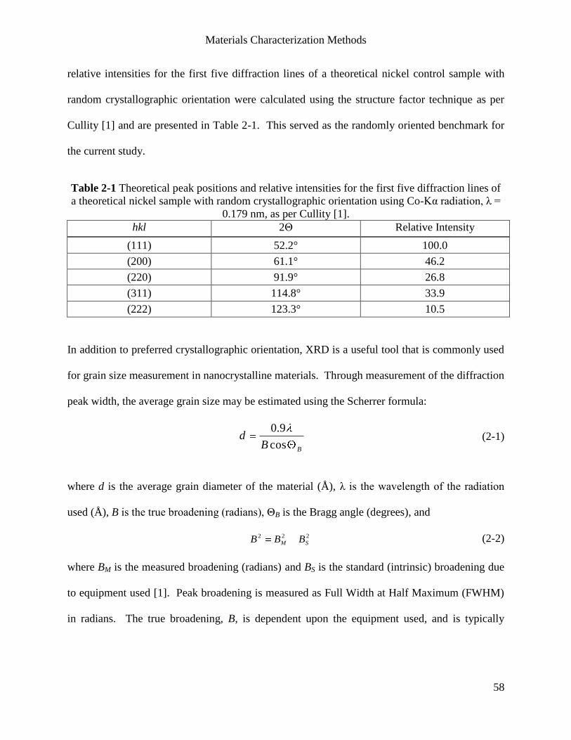
Materials Characterization Methods
58
relative intensities for the first five diffraction lines of a theoretical nickel control sample with
random crystallographic orientation were calculated using the structure factor technique as per
Cullity [1] and are presented in Table 2-1. This served as the randomly oriented benchmark for
the current study.
Table 2-1 Theoretical peak positions and relative intensities for the first five diffraction lines of
a theoretical nickel sample with random crystallographic orientation using Co-Kα radiation, λ =
0.179 nm, as per Cullity [1].
hkl 2Θ Relative Intensity
(111) 52.2° 100.0
(200) 61.1° 46.2
(220) 91.9° 26.8
(311) 114.8° 33.9
(222) 123.3° 10.5
In addition to preferred crystallographic orientation, XRD is a useful tool that is commonly used
for grain size measurement in nanocrystalline materials. Through measurement of the diffraction
peak width, the average grain size may be estimated using the Scherrer formula:
BBd
cos
9.0 (2-1)
where d is the average grain diameter of the material (Å), λ is the wavelength of the radiation
used (Å), B is the true broadening (radians), ΘB is the Bragg angle (degrees), and
222
SM BBB (2-2)
where BM is the measured broadening (radians) and BS is the standard (intrinsic) broadening due
to equipment used [1]. Peak broadening is measured as Full Width at Half Maximum (FWHM)
in radians. The true broadening, B, is dependent upon the equipment used, and is typically
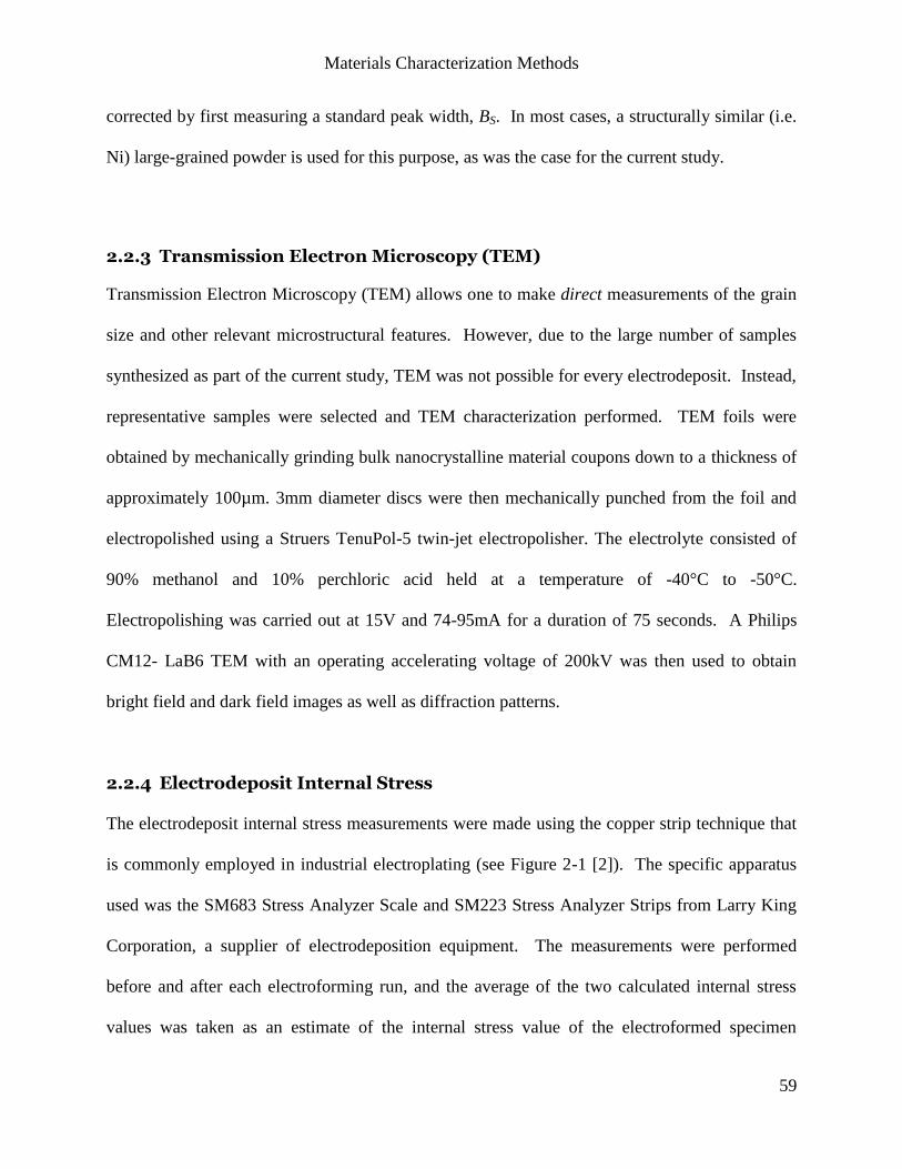
Materials Characterization Methods
59
corrected by first measuring a standard peak width, BS. In most cases, a structurally similar (i.e.
Ni) large-grained powder is used for this purpose, as was the case for the current study.
2.2.3 Transmission Electron Microscopy (TEM)
Transmission Electron Microscopy (TEM) allows one to make direct measurements of the grain
size and other relevant microstructural features. However, due to the large number of samples
synthesized as part of the current study, TEM was not possible for every electrodeposit. Instead,
representative samples were selected and TEM characterization performed. TEM foils were
obtained by mechanically grinding bulk nanocrystalline material coupons down to a thickness of
approximately 100µm. 3mm diameter discs were then mechanically punched from the foil and
electropolished using a Struers TenuPol-5 twin-jet electropolisher. The electrolyte consisted of
90% methanol and 10% perchloric acid held at a temperature of -40°C to -50°C.
Electropolishing was carried out at 15V and 74-95mA for a duration of 75 seconds. A Philips
CM12- LaB6 TEM with an operating accelerating voltage of 200kV was then used to obtain
bright field and dark field images as well as diffraction patterns.
2.2.4 Electrodeposit Internal Stress
The electrodeposit internal stress measurements were made using the copper strip technique that
is commonly employed in industrial electroplating (see Figure 2-1 [2]). The specific apparatus
used was the SM683 Stress Analyzer Scale and SM223 Stress Analyzer Strips from Larry King
Corporation, a supplier of electrodeposition equipment. The measurements were performed
before and after each electroforming run, and the average of the two calculated internal stress
values was taken as an estimate of the internal stress value of the electroformed specimen
Materials Characterization Methods
60
synthesized chronologically between. In other words, the internal stress values presented for
each nanocrystalline specimen are not direct measurements made of the specimen itself, but are
instead the average of the two witness samples carried out immediately before and after the
specimen of interest. The electroplating / electroforming convention for the directionality of
internal stress has been maintained, with “tensile” stress referring to the propensity for each layer
of the growing electrodeposit to cause progressive macroscopic plate contraction – see Figure 2-
1(b).
Figure 2-1 Side view schematic of the internal stress measurement apparatus showing the
initially flat Cu foil strip onto which the material in question is electrodeposited (shown as the
curved black line) clamped by a screw at the top of the fixture and permitted to bend naturally.
When the electrodeposited coating exhibits tensile residual stress, the direction of deflection is
opposite the case when the electrodeposit stress is compressive in nature (both cases are shown
in the figure). The amount of deflection of the bottom edge of the foil is measured using a
graduated scale at the bottom of the apparatus, with this scale having been calibrated by the
manufacturer in such a way that a value for the electrodeposited coating residual stress level may
be calculated [2].
a) b)
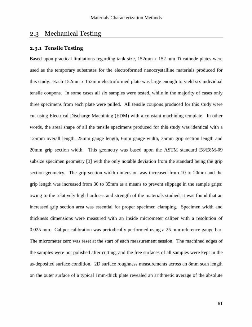
Materials Characterization Methods
61
2.3 Mechanical Testing
2.3.1 Tensile Testing
Based upon practical limitations regarding tank size, 152mm x 152 mm Ti cathode plates were
used as the temporary substrates for the electroformed nanocrystalline materials produced for
this study. Each 152mm x 152mm electroformed plate was large enough to yield six individual
tensile coupons. In some cases all six samples were tested, while in the majority of cases only
three specimens from each plate were pulled. All tensile coupons produced for this study were
cut using Electrical Discharge Machining (EDM) with a constant machining template. In other
words, the areal shape of all the tensile specimens produced for this study was identical with a
125mm overall length, 25mm gauge length, 6mm gauge width, 35mm grip section length and
20mm grip section width. This geometry was based upon the ASTM standard E8/E8M-09
subsize specimen geometry [3] with the only notable deviation from the standard being the grip
section geometry. The grip section width dimension was increased from 10 to 20mm and the
grip length was increased from 30 to 35mm as a means to prevent slippage in the sample grips;
owing to the relatively high hardness and strength of the materials studied, it was found that an
increased grip section area was essential for proper specimen clamping. Specimen width and
thickness dimensions were measured with an inside micrometer caliper with a resolution of
0.025 mm. Caliper calibration was periodically performed using a 25 mm reference gauge bar.
The micrometer zero was reset at the start of each measurement session. The machined edges of
the samples were not polished after cutting, and the free surfaces of all samples were kept in the
as-deposited surface condition. 2D surface roughness measurements across an 8mm scan length
on the outer surface of a typical 1mm-thick plate revealed an arithmetic average of the absolute
Materials Characterization Methods
62
values (Ra) of approximately 1 micron. See Figure 2-2 for a photograph of typical specimens
before and after tensile testing.
All tensile tests were performed at Engineering Materials Research Inc. (Toronto, Ontario) using
a 67 kN capacity servo hydraulic load frame configured with a MTS controller. The load frame
was calibrated annually using load standards traceable to United States National Institute of
Standards and Technology (NIST). A pair of hydraulically actuated wedge grips was installed in
the load frame to grip the specimen.
Tensile tests were conducted using displacement control and a ramp waveform at a rate of
approx 0.1 mm/min in lab air and 20-25°C. All tensile tests were carried out at a strain rate of
5x10⁻⁴
s-1
and were typically performed until the specimen fractured. Results were recorded by
a computer data acquisition system. Prior to each test, the data acquisition system was
calibrated using a voltmeter which was calibrated at approximately 1 year intervals. All samples
were tested to fracture and the elongation to fracture, εf, was measured using both a calibrated
extensometer and also by measurement of the gauge length before and after testing. An MTS
Figure 2-2 Photograph of typical specimens (Ni-6.4wt%Fe; 18nm average grain size) before
and after tensile testing in conformance with ASTM E8 [3]. Scale in cm.
Materials Characterization Methods
63
Model 632.11C-20 extensometer with a 25 mm gauge length and a maximum measuring range
of 3.5 mm was used to measure specimen gauge length displacement. The extensometer was
calibrated by following the ASTM Standard Practice for Verification and Classification of
Extensometers and met the requirements of Class B-1 [4]. The extensometer was mounted at
approximately the center of the specimen's gauge length.
Several methods have been used to determine the maximum uniform strain including the
graphical method, the Considère criterion, and the point of peak load on the stress-strain curve
[5]. In the case of the Considère criterion, different relationships are used depending on whether
plastic instability occurs by diffuse necking (dσ/dε = σ) such as in the case of round bar, or by
localized necking (dσ/dε = σ/2) such as in the case of thin flat sheet [6,7]. These two necking
modes are illustrated in Figure 1-13. Many of the samples of the present study exhibited a mixed
mode of necking failure. Consequently, the peak load method was used to designate the onset of
plastic instability in order to determine the maximum uniform strain. The elastic component of
the maximum uniform strain was assumed to be equivalent to the strain measured from the onset
of loading until the 0.2% offset yield point [3] with elastic strain values typically falling within
the range of 0.5 to 1%. The difference between the measured maximum uniform strain (at peak
load) and the elastic strain term was then termed the maximum uniform plastic strain.
The strain hardening exponent was calculated using ASTM E646, “Standard Test Method for
Tensile Strain-Hardening Exponents (n-Values) of Metallic Sheet Materials” [8]. This method
involves fitting the plastic portion of the true stress-true strain curve to the power law
relationship Equation (1-9). While this exercise may be performed over any portion of the
Materials Characterization Methods
64
plastic flow curve, fitting of the present study was carried out from the 0.2% offset yield point
until the onset of necking.
2.3.2 Vickers Microhardness
Hardness measurements were performed using the Vickers microhardness technique by
measuring the averages of at least 10 indentations each at several locations on each
electrodeposit. The applied loads were 50-200 g depending on the deposit thickness. In all cases,
the sample thickness was at least 20 times the depth of individual indentations. Samples were
mounted into epoxy before measurements were made in order to ensure proper specimen support
and therefore provide accurate readings.
2.4 References
[1] B.D. Cullity, Elements of X-ray Diffraction, second ed., Addison-Wesley, Reading (MA),
1978, p.102.
[2] B. Stein, AESF Electroforming Symposium, March 27-29, 1996, Las Vegas, NV.
[3] ASTM Standard E8M-01 (2001) ASTM International, West Conshohocken, PA.
[4] ASTM E83-98 (1998) ASTM International, West Conshohocken, PA
[5] G.E. Dieter, Mechanical Metallurgy, SI Metric ed., McGraw-Hill, London, 1988, p.370.
[6] C.C. Koch, K.M. Youssef, R.O. Scattergood, K.L. Murty, Adv. Eng. Mater. 7,9 (2005) 797.
[7] A. Misra, X. Zhang, D. Hammon, R.G. Hoagland, Acta Mater. 53 (2005) 221.
[8] ASTM Standard E646-07 (2007) ASTM International, West Conshohocken, PA.
65
Chapter 3 Materials Synthesis
3.1 Introduction
As described in Chapter 1, the characteristics of the nanostructured material synthesis method
can play a major role in the observed response to subsequent mechanical deformation. This has
made it difficult, and in many cases impossible, to de-convolute the effect(s) of nanocrystalline
grain refinement from those originating from other concomitant structural characteristics such as
porosity, particulate contamination, chemical contamination, secondary phases, internal stress,
and other side effects of the technique used to create the nano-sized crystals. Therefore, one
main objective of this study was the elimination or minimization of synthesis artifacts in the
nanocrystalline material electrodeposition process.
The second objective of this study was to answer the question of whether it is possible to
synthesize bulk quantities of electrodeposited nanocrystalline materials to enable tensile testing
in conformance with ASTM E8 since, prior to this study, reproducible nanomaterial thick plate
electroforming had not been possible. Thus, the main contributions of this chapter are the
description of the issues associated with electrodeposition-based synthesis of bulk quantities of
artifact-reduced nanocrystalline materials and how they were overcome.
Materials Synthesis
66
3.2 Nomenclature
A few remarks on nomenclature are appropriate to begin. “Electrodeposition” refers to the
electrochemical reduction of one or more dissolved metallic species from an electrically
conductive electrolyte, as will be described in Section 3.3. “Electroplating” is the term most
commonly used to describe industrial-scale electrodeposition processes, and refers specifically to
the coating of a substrate with a layer of electrodeposited material. Generally, this layer is
relatively thin (say, 1-50µm) and is used for superficial purposes e.g. 10µm layer of Zn as a
galvanic corrosion protection coating on steel, 15µm of duplex Ni/Cr on steel for corrosion
resistance, surface hardness, and aesthetic quality, 5µm Cu throughhole plating to electrically
connect the laminates in a printed circuit board panel, and so on. In other words,
“electroplating” refers to coating a substrate using an electrodeposition-based process.
On the other hand, it may be desirable to create structures comprised wholly of the
electrodeposited material. In this case, one would electrodeposit for a much longer period of
time in order to create a much thicker layer of material e.g. >200µm. The material would be
electrodeposited onto a temporary substrate, and then subsequently removed for use. This
process is commonly known as “electroforming” and may also be considered a subset of
“electrodeposition”. For the present study, the objective is to evaluate the properties of the
electrodeposited material itself without any influence of the substrate. Hence, all specimens
discussed here have been “electroformed” onto temporary commercial grade pure Ti cathode
substrates from which they were subsequently stripped to yield free-standing sheets to be cut into
specimens for characterization and mechanical testing. The removal of the nanocrystalline plate
was accomplished by lifting the nanocrystalline plate from the temporary Ti cathode substrate.
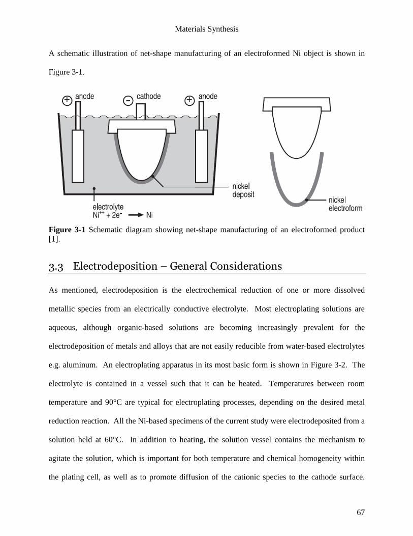
Materials Synthesis
67
A schematic illustration of net-shape manufacturing of an electroformed Ni object is shown in
Figure 3-1.
Figure 3-1 Schematic diagram showing net-shape manufacturing of an electroformed product
[1].
3.3 Electrodeposition – General Considerations
As mentioned, electrodeposition is the electrochemical reduction of one or more dissolved
metallic species from an electrically conductive electrolyte. Most electroplating solutions are
aqueous, although organic-based solutions are becoming increasingly prevalent for the
electrodeposition of metals and alloys that are not easily reducible from water-based electrolytes
e.g. aluminum. An electroplating apparatus in its most basic form is shown in Figure 3-2. The
electrolyte is contained in a vessel such that it can be heated. Temperatures between room
temperature and 90°C are typical for electroplating processes, depending on the desired metal
reduction reaction. All the Ni-based specimens of the current study were electrodeposited from a
solution held at 60°C. In addition to heating, the solution vessel contains the mechanism to
agitate the solution, which is important for both temperature and chemical homogeneity within
the plating cell, as well as to promote diffusion of the cationic species to the cathode surface.
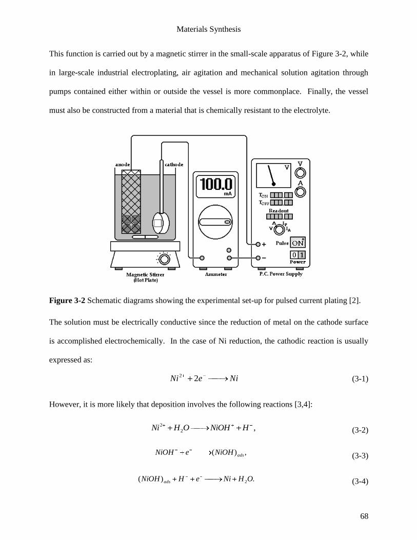
Materials Synthesis
68
This function is carried out by a magnetic stirrer in the small-scale apparatus of Figure 3-2, while
in large-scale industrial electroplating, air agitation and mechanical solution agitation through
pumps contained either within or outside the vessel is more commonplace. Finally, the vessel
must also be constructed from a material that is chemically resistant to the electrolyte.
Figure 3-2 Schematic diagrams showing the experimental set-up for pulsed current plating [2].
The solution must be electrically conductive since the reduction of metal on the cathode surface
is accomplished electrochemically. In the case of Ni reduction, the cathodic reaction is usually
expressed as:
(3-1)
However, it is more likely that deposition involves the following reactions [3,4]:
(3-2)
(3-3)
(3-4)
NieNi 22
,2
2 HNiOHOHNi
,)( adsNiOHeNiOH
.)( 2OHNieHNiOH ads
Materials Synthesis
69
Current is supplied by an external power source (shown with an ammeter in series for the
particular example shown in Figure 3-2) and the circuit is completed by the anode-cathode
electrode couple immersed in the electrolyte. In principle, the negatively-polarized cathode may
be any electrically conductive material that is chemically resistant to the plating solution, while
the positively-charged anode may be either a non-consumable dimensionally stable anode such
as Pt-clad Nb or a consumable anode that oxidizes as electrodeposition proceeds. For the current
study, the predominant anode material was “R-rounds”, a form of pure Ni manufactured by
INCO mainly for the specific application of plating anodes. INCO R-rounds are perhaps the
most commonly used anode material in industrial Ni electroplating and electroforming. The R-
rounds were held in a Ti basket as is conventional plating practice. As the electrodeposition
process proceeds, metallic Ni from the R-rounds continuously oxidizes and enters the solution in
cationic form, while any unoxidized Ni particulate is captured in a cloth anode bag that
encapsulates the Ti basket. Electrodeposition using a dimensionally stable anode, on the other
hand, requires the continuous external replenishment of the cationic species to be reduced. In
the case of Ni electrodeposition, this may be accomplished by the addition of NiCO3 dissolved in
water, for instance. Electrodeposition using a dimensionally stable anode was not performed as
part of the current study.
Materials Synthesis
70
3.4 Electrodeposition for the Production of Fine-Grained Microstructures
It is possible to create materials across a very broad spectrum of microstructures using the
electrodeposition synthesis method. Metals such as tin, lead and zinc may exhibit average grain
size values on the order of 10µm or larger when deposited from an additive-free bath. On the
other hand, metals from the iron-group (Ni, Fe, Co), some of the precious metals e.g. Au, Pt, Rh,
and a number of others can be electrodeposited in nanocrystalline form through proper control of
the chemical and electrical processing parameters [5,6]. In fact, with some systems,
microstructural refinement through to the amorphous regime can be accomplished if so desired.
A notable example includes electrolytic Ni-P deposition under conditions where the deposit
chemical composition exceeds approximately 6wt%P [7]. Many Cr electrodeposits are also
known to be amorphous. Cross-sectional images and accompanying schematics corresponding
to a typical coarse-grained electrodeposit compared to a chemically similar nanocrystalline
electrodeposit are shown in Figure 3-3. With increasing grain refinement, the crystal
morphology typically transitions from columnar (e.g. Figure 3-3(a)) to fibrous (i.e. a finer, more
narrow columnar grain shape) to equiaxed (e.g. Figure 3-3(b)). This grain shape transition from
columnar to fibrous to equiaxed is a general trend for many electrodeposited materials such as
Cu and Ni. In other words, through control of the material synthesis parameters, it is possible to
achieve a Cu deposit, for instance, that exhibits a columnar morphology of 10µm average grain
size, or through grain refinement, an equiaxed nanocrystalline one that exhibits microstructure
orders of magnitude finer.
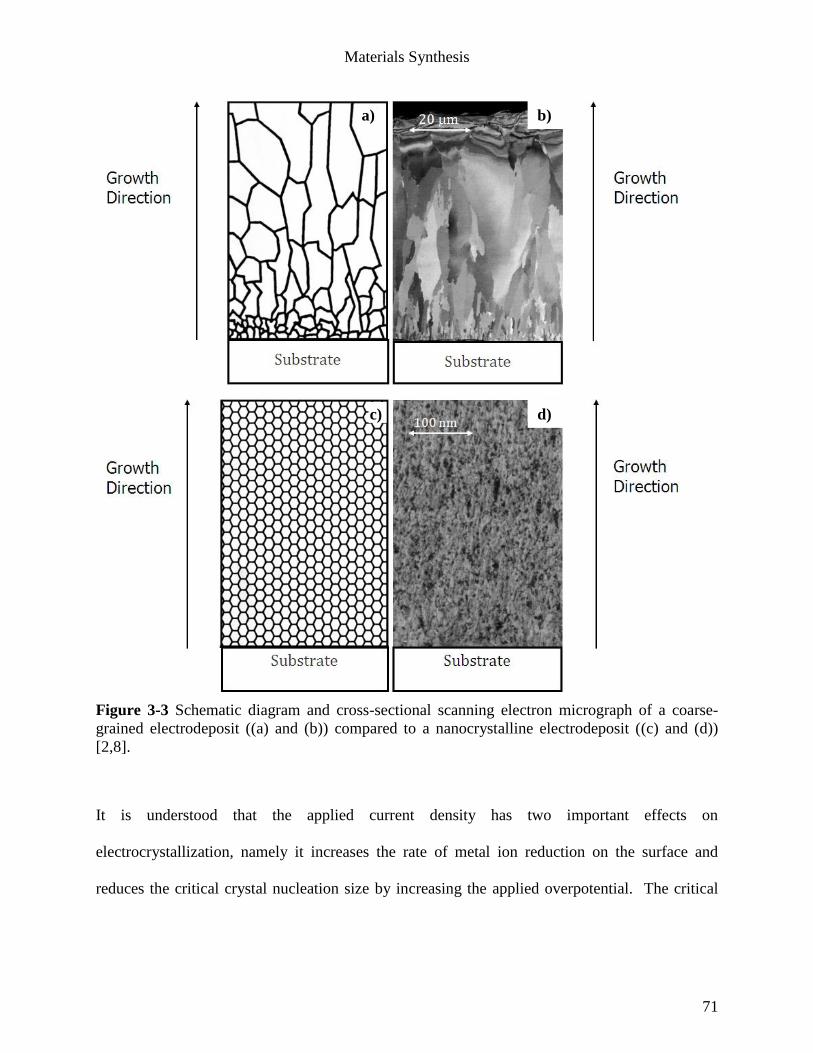
Materials Synthesis
71
Figure 3-3 Schematic diagram and cross-sectional scanning electron micrograph of a coarse-
grained electrodeposit ((a) and (b)) compared to a nanocrystalline electrodeposit ((c) and (d))
[2,8].
It is understood that the applied current density has two important effects on
electrocrystallization, namely it increases the rate of metal ion reduction on the surface and
reduces the critical crystal nucleation size by increasing the applied overpotential. The critical
d)
b)
a)
c)
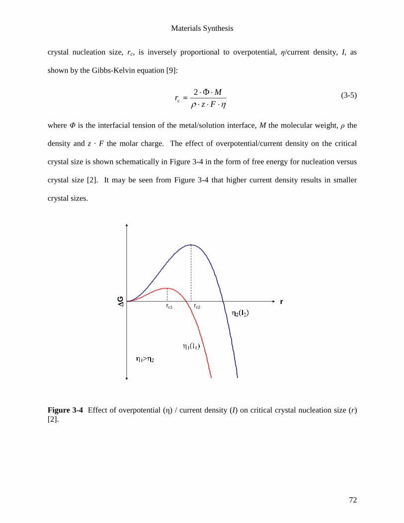
Materials Synthesis
72
rG
rc2rc1
crystal nucleation size, rc, is inversely proportional to overpotential, η/current density, I, as
shown by the Gibbs-Kelvin equation [9]:
(3-5)
where Φ is the interfacial tension of the metal/solution interface, M the molecular weight, ρ the
density and z · F the molar charge. The effect of overpotential/current density on the critical
crystal size is shown schematically in Figure 3-4 in the form of free energy for nucleation versus
crystal size [2]. It may be seen from Figure 3-4 that higher current density results in smaller
crystal sizes.
Figure 3-4 Effect of overpotential (η) / current density (I) on critical crystal nucleation size (r)
[2].
Fz
Mrc
2
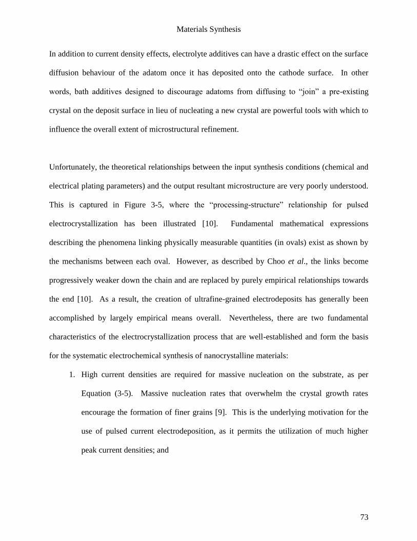
Materials Synthesis
73
In addition to current density effects, electrolyte additives can have a drastic effect on the surface
diffusion behaviour of the adatom once it has deposited onto the cathode surface. In other
words, bath additives designed to discourage adatoms from diffusing to “join” a pre-existing
crystal on the deposit surface in lieu of nucleating a new crystal are powerful tools with which to
influence the overall extent of microstructural refinement.
Unfortunately, the theoretical relationships between the input synthesis conditions (chemical and
electrical plating parameters) and the output resultant microstructure are very poorly understood.
This is captured in Figure 3-5, where the “processing-structure” relationship for pulsed
electrocrystallization has been illustrated [10]. Fundamental mathematical expressions
describing the phenomena linking physically measurable quantities (in ovals) exist as shown by
the mechanisms between each oval. However, as described by Choo et al., the links become
progressively weaker down the chain and are replaced by purely empirical relationships towards
the end [10]. As a result, the creation of ultrafine-grained electrodeposits has generally been
accomplished by largely empirical means overall. Nevertheless, there are two fundamental
characteristics of the electrocrystallization process that are well-established and form the basis
for the systematic electrochemical synthesis of nanocrystalline materials:
1. High current densities are required for massive nucleation on the substrate, as per
Equation (3-5). Massive nucleation rates that overwhelm the crystal growth rates
encourage the formation of finer grains [9]. This is the underlying motivation for the
use of pulsed current electrodeposition, as it permits the utilization of much higher
peak current densities; and
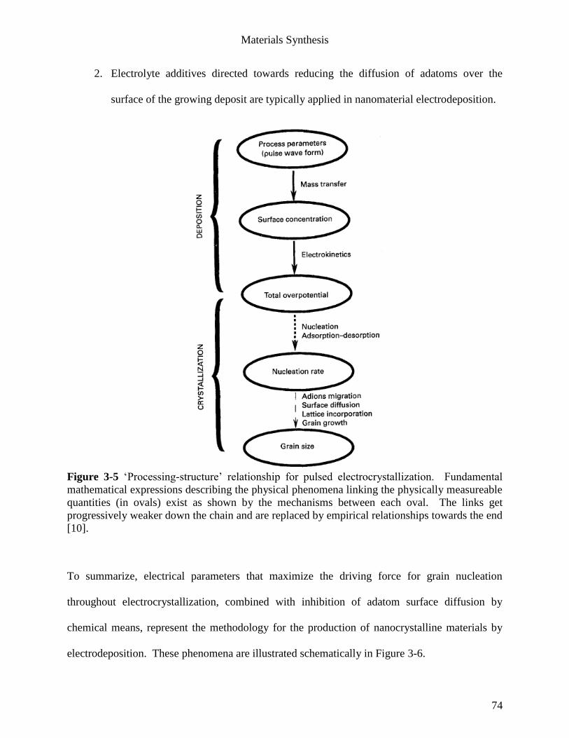
Materials Synthesis
74
2. Electrolyte additives directed towards reducing the diffusion of adatoms over the
surface of the growing deposit are typically applied in nanomaterial electrodeposition.
Figure 3-5 „Processing-structure‟ relationship for pulsed electrocrystallization. Fundamental
mathematical expressions describing the physical phenomena linking the physically measureable
quantities (in ovals) exist as shown by the mechanisms between each oval. The links get
progressively weaker down the chain and are replaced by empirical relationships towards the end
[10].
To summarize, electrical parameters that maximize the driving force for grain nucleation
throughout electrocrystallization, combined with inhibition of adatom surface diffusion by
chemical means, represent the methodology for the production of nanocrystalline materials by
electrodeposition. These phenomena are illustrated schematically in Figure 3-6.
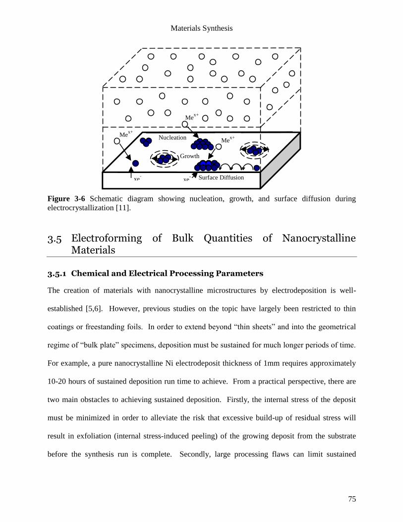
Materials Synthesis
75
Mex+
Growth
Mex+
Nucleation
xe-
Mex+
Surface Diffusion CMex+
C∞
x
xe-
Figure 3-6 Schematic diagram showing nucleation, growth, and surface diffusion during
electrocrystallization [11].
3.5 Electroforming of Bulk Quantities of Nanocrystalline Materials
3.5.1 Chemical and Electrical Processing Parameters
The creation of materials with nanocrystalline microstructures by electrodeposition is well-
established [5,6]. However, previous studies on the topic have largely been restricted to thin
coatings or freestanding foils. In order to extend beyond “thin sheets” and into the geometrical
regime of “bulk plate” specimens, deposition must be sustained for much longer periods of time.
For example, a pure nanocrystalline Ni electrodeposit thickness of 1mm requires approximately
10-20 hours of sustained deposition run time to achieve. From a practical perspective, there are
two main obstacles to achieving sustained deposition. Firstly, the internal stress of the deposit
must be minimized in order to alleviate the risk that excessive build-up of residual stress will
result in exfoliation (internal stress-induced peeling) of the growing deposit from the substrate
before the synthesis run is complete. Secondly, large processing flaws can limit sustained
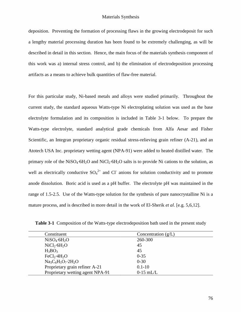
Materials Synthesis
76
deposition. Preventing the formation of processing flaws in the growing electrodeposit for such
a lengthy material processing duration has been found to be extremely challenging, as will be
described in detail in this section. Hence, the main focus of the materials synthesis component of
this work was a) internal stress control, and b) the elimination of electrodeposition processing
artifacts as a means to achieve bulk quantities of flaw-free material.
For this particular study, Ni-based metals and alloys were studied primarily. Throughout the
current study, the standard aqueous Watts-type Ni electroplating solution was used as the base
electrolyte formulation and its composition is included in Table 3-1 below. To prepare the
Watts-type electrolyte, standard analytical grade chemicals from Alfa Aesar and Fisher
Scientific, an Integran proprietary organic residual stress-relieving grain refiner (A-21), and an
Atotech USA Inc. proprietary wetting agent (NPA-91) were added to heated distilled water. The
primary role of the NiSO4·6H2O and NiCl2·6H2O salts is to provide Ni cations to the solution, as
well as electrically conductive SO42+
and Cl- anions for solution conductivity and to promote
anode dissolution. Boric acid is used as a pH buffer. The electrolyte pH was maintained in the
range of 1.5-2.5. Use of the Watts-type solution for the synthesis of pure nanocrystalline Ni is a
mature process, and is described in more detail in the work of El-Sherik et al. [e.g. 5,6,12].
Table 3-1 Composition of the Watts-type electrodeposition bath used in the present study
Constituent Concentration (g/L)
NiSO4·6H2O 260-300
NiCl2·6H2O 45
H3BO3 45
FeCl2·4H2O 0-35
Na3C6H5O7·2H2O 0-30
Proprietary grain refiner A-21 0.1-10
Proprietary wetting agent NPA-91 0-15 mL/L
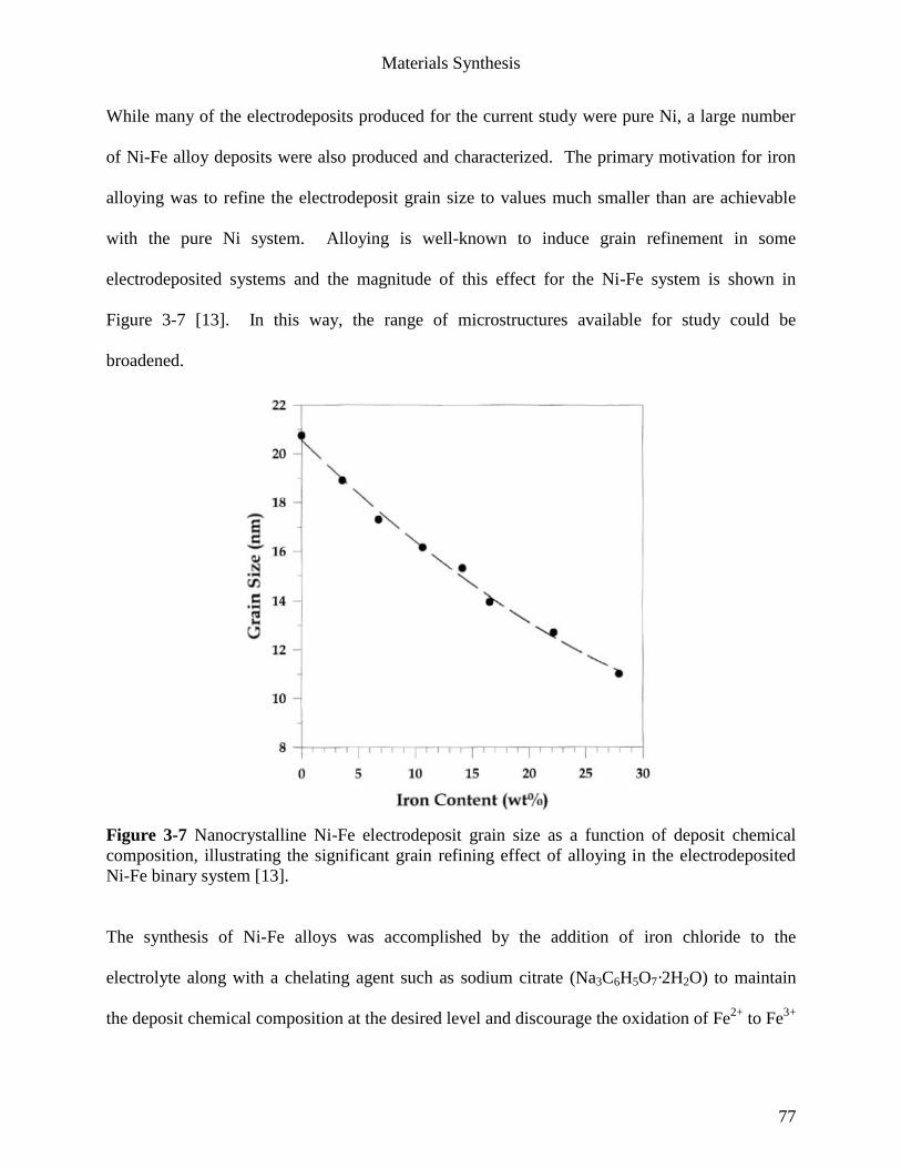
Materials Synthesis
77
While many of the electrodeposits produced for the current study were pure Ni, a large number
of Ni-Fe alloy deposits were also produced and characterized. The primary motivation for iron
alloying was to refine the electrodeposit grain size to values much smaller than are achievable
with the pure Ni system. Alloying is well-known to induce grain refinement in some
electrodeposited systems and the magnitude of this effect for the Ni-Fe system is shown in
Figure 3-7 [13]. In this way, the range of microstructures available for study could be
broadened.
Figure 3-7 Nanocrystalline Ni-Fe electrodeposit grain size as a function of deposit chemical
composition, illustrating the significant grain refining effect of alloying in the electrodeposited
Ni-Fe binary system [13].
The synthesis of Ni-Fe alloys was accomplished by the addition of iron chloride to the
electrolyte along with a chelating agent such as sodium citrate (Na3C6H5O7·2H2O) to maintain
the deposit chemical composition at the desired level and discourage the oxidation of Fe2+
to Fe3+
Materials Synthesis
78
(see Table 3-1). As described by Cheung et al., Fe3+
tends to form iron oxide (Fe2O3) precipitate
in the presence of dissolved oxygen in the electrolyte, the end result being that Fe-containing
plating solutions may be short-lived [13]. In addition to dissolved iron salts and chelating
agents, electrolytic Fe was added as an anode material so that the solution could be continuously
replenished with both Ni and Fe cations during the electrodeposition process. A schematic
diagram and photograph of the apparatus developed for the materials synthesis in this study are
shown in Figure 3-8 below. Nanocrystalline Ni-Fe electrodeposition is also a mature process
and more information is provided by Cheung et al. [13-16].
In addition to pure Ni and Ni-Fe alloy electrodeposits, some Co-based materials along with data
from past studies in the literature were added to the Chapter 5 study of hardness-strength
relationships in order to broaden the data set. The synthesis of these materials will not be
described here, but more information can be found in the individual works cited in Chapter 5.
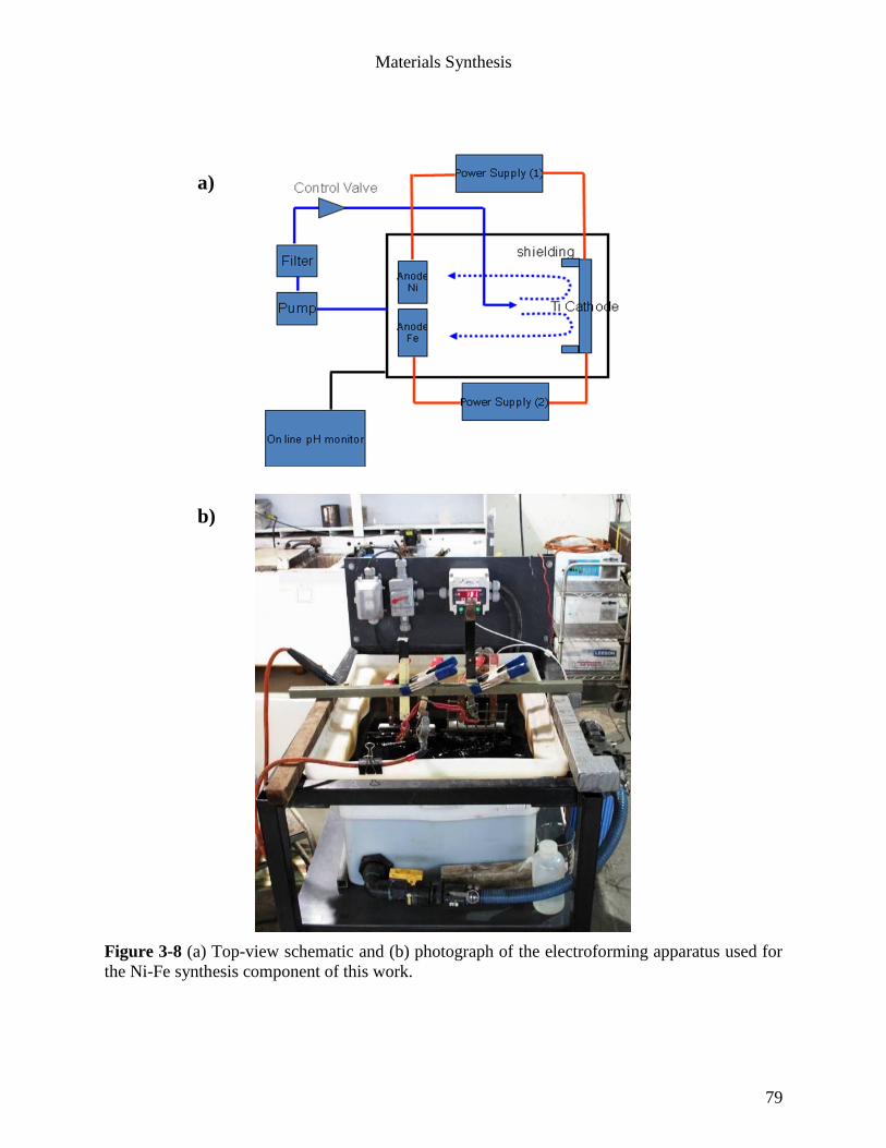
Materials Synthesis
79
Figure 3-8 (a) Top-view schematic and (b) photograph of the electroforming apparatus used for
the Ni-Fe synthesis component of this work.
a)
b)
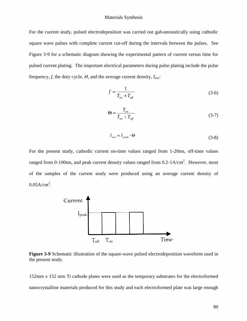
Materials Synthesis
80
For the current study, pulsed electrodeposition was carried out galvanostatically using cathodic
square wave pulses with complete current cut-off during the intervals between the pulses. See
Figure 3-9 for a schematic diagram showing the experimental pattern of current versus time for
pulsed current plating. The important electrical parameters during pulse plating include the pulse
frequency, f, the duty cycle, Θ, and the average current density, Iave:
(3-6)
(3-7)
(3-8)
For the present study, cathodic current on-time values ranged from 1-20ms, off-time values
ranged from 0-100ms, and peak current density values ranged from 0.2-1A/cm2. However, most
of the samples of the current study were produced using an average current density of
0.05A/cm2.
Figure 3-9 Schematic illustration of the square-wave pulsed electrodeposition waveform used in
the present study.
152mm x 152 mm Ti cathode plates were used as the temporary substrates for the electroformed
nanocrystalline materials produced for this study and each electroformed plate was large enough
offon TTf
1
offon
on
TT
T
peakave II
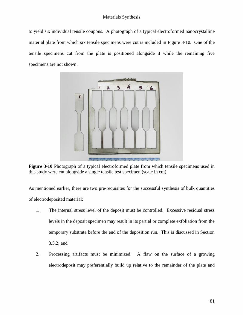
Materials Synthesis
81
to yield six individual tensile coupons. A photograph of a typical electroformed nanocrystalline
material plate from which six tensile specimens were cut is included in Figure 3-10. One of the
tensile specimens cut from the plate is positioned alongside it while the remaining five
specimens are not shown.
Figure 3-10 Photograph of a typical electroformed plate from which tensile specimens used in
this study were cut alongside a single tensile test specimen (scale in cm).
As mentioned earlier, there are two pre-requisites for the successful synthesis of bulk quantities
of electrodeposited material:
1. The internal stress level of the deposit must be controlled. Excessive residual stress
levels in the deposit specimen may result in its partial or complete exfoliation from the
temporary substrate before the end of the deposition run. This is discussed in Section
3.5.2; and
2. Processing artifacts must be minimized. A flaw on the surface of a growing
electrodeposit may preferentially build up relative to the remainder of the plate and
Materials Synthesis
82
eventually inhibit or prevent sustained deposition altogether. Processing flaws are
discussed in detail in Section 3.5.3.
3.5.2 Internal Stress Control
Internal stress is a common characteristic of electrodeposited materials (irrespective of grain
size) and can limit the upper plate thickness that may be achieved. There are several structural
causes of this electrodeposit internal “macrostress”, as outlined by Weil [17]: “If the interatomic
spacing of an epitaxial deposit is different from that of the substrate on which it is forced to fit,
macrostresses develop. If the coefficients of thermal expansion of the substrate and deposit differ
and plating is carried out at elevated temperatures, macrostresses develop in cooling.
Codeposited hydrogen can affect the internal stress by diffusing into the substrate and expanding
it while the deposit tries to contract. Diffusion of hydrogen from the near-surface region toward
the substrate can also result in a tensile macrostress. Recrystallization and decomposition of
hydrides or other compounds are also possible causes of macrostresses.” Regardless of its
origin, internal stress-relieving electrolyte additives are commonly employed in industrial
electroforming i.e. where the production of thick freestanding electrodeposits is desired. A
commonly used rule of thumb is that the internal stress of an electroform to exceed 2mm in
thickness must be maintained below approximately 7MPa in order to avoid gross dimensional
non-conformity due to residual stress-induced deflection [18].
For the Watts Ni system, electrolyte grain refiner concentrations in the range of 0.1 – 0.5 g/L are
typically used to minimize deposit stress, a common practice in thick plate electroforming, see
Figure 3-11(a) [19]. Using the standard Watts-type Ni electrolyte of Table 3-1, the stress-
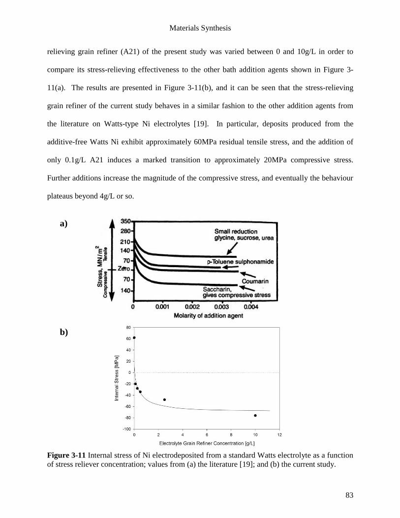
Materials Synthesis
83
relieving grain refiner (A21) of the present study was varied between 0 and 10g/L in order to
compare its stress-relieving effectiveness to the other bath addition agents shown in Figure 3-
11(a). The results are presented in Figure 3-11(b), and it can be seen that the stress-relieving
grain refiner of the current study behaves in a similar fashion to the other addition agents from
the literature on Watts-type Ni electrolytes [19]. In particular, deposits produced from the
additive-free Watts Ni exhibit approximately 60MPa residual tensile stress, and the addition of
only 0.1g/L A21 induces a marked transition to approximately 20MPa compressive stress.
Further additions increase the magnitude of the compressive stress, and eventually the behaviour
plateaus beyond 4g/L or so.
Figure 3-11 Internal stress of Ni electrodeposited from a standard Watts electrolyte as a function
of stress reliever concentration; values from (a) the literature [19]; and (b) the current study.
a)
b)
Materials Synthesis
84
One notable characteristic of Figure 3-11(b) is the steep slope of the curve in the proximity of 0
MPa internal stress. The significance of this high slope is that, in an attempt to achieve a state of
zero stress, small changes in the effective stress-relieving grain refiner concentration may induce
significant changes in the observed residual stress of the resulting electrodeposit. Unfortunately,
the maintenance of a steady-state stress-relieving bath addition agent concentration is non-trivial,
as will be explained below.
Typical organic stress-relievers, such as the one employed in the current study, actively
participate in the electrocrystallization process and tend to become at least partially co-deposited
within the Ni deposit as it grows [20]. In other words, the additive is continuously consumed by
the process. Moreover, there is a well-known tendency for organic electroforming bath additives
to decompose in service wherein the intermediate compounds (or breakdown products) are in
fact the predominant species with respect to modification of the electrodeposit properties [20].
For instance, Figure 3-12 contains the results of a study of the decomposition products of
benzoic acid sulfimide in Ni electrodeposition [20]. The “age” of the bath is represented by the
total amount of electrical charge passed through the system per unit electrolyte volume. The
original additive molecule, benzoic acid sulfimide, decomposes into numerous sub-species as
electrodeposition proceeds. Two of these decomposition products, o-toluene sulfonamide and
benzamide, were monitored and attempts were made to correlate their concentration to
electrodeposit internal stress and other properties, with limited success. Numerous such attempts
have been made to differentiate between the individual decomposition product species and their
effects on the resultant electrodeposit microstructure [20]. Unfortunately, the complexity of the
electrocrystallization process (e.g. [10]) combined with the numerous possibilities for
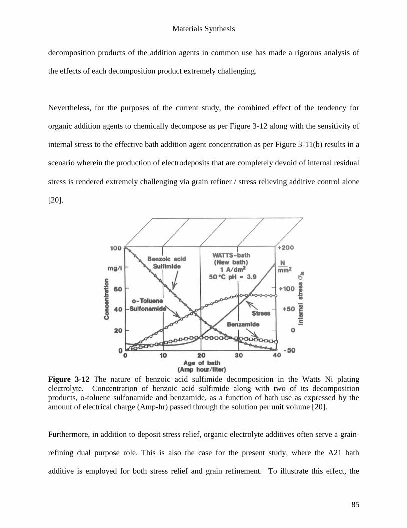
Materials Synthesis
85
decomposition products of the addition agents in common use has made a rigorous analysis of
the effects of each decomposition product extremely challenging.
Nevertheless, for the purposes of the current study, the combined effect of the tendency for
organic addition agents to chemically decompose as per Figure 3-12 along with the sensitivity of
internal stress to the effective bath addition agent concentration as per Figure 3-11(b) results in a
scenario wherein the production of electrodeposits that are completely devoid of internal residual
stress is rendered extremely challenging via grain refiner / stress relieving additive control alone
[20].
Figure 3-12 The nature of benzoic acid sulfimide decomposition in the Watts Ni plating
electrolyte. Concentration of benzoic acid sulfimide along with two of its decomposition
products, o-toluene sulfonamide and benzamide, as a function of bath use as expressed by the
amount of electrical charge (Amp-hr) passed through the solution per unit volume [20].
Furthermore, in addition to deposit stress relief, organic electrolyte additives often serve a grain-
refining dual purpose role. This is also the case for the present study, where the A21 bath
additive is employed for both stress relief and grain refinement. To illustrate this effect, the
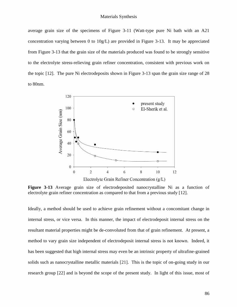
Materials Synthesis
86
average grain size of the specimens of Figure 3-11 (Watt-type pure Ni bath with an A21
concentration varying between 0 to 10g/L) are provided in Figure 3-13. It may be appreciated
from Figure 3-13 that the grain size of the materials produced was found to be strongly sensitive
to the electrolyte stress-relieving grain refiner concentration, consistent with previous work on
the topic [12]. The pure Ni electrodeposits shown in Figure 3-13 span the grain size range of 28
to 80nm.
Figure 3-13 Average grain size of electrodeposited nanocrystalline Ni as a function of
electrolyte grain refiner concentration as compared to that from a previous study [12].
Ideally, a method should be used to achieve grain refinement without a concomitant change in
internal stress, or vice versa. In this manner, the impact of electrodeposit internal stress on the
resultant material properties might be de-convoluted from that of grain refinement. At present, a
method to vary grain size independent of electrodeposit internal stress is not known. Indeed, it
has been suggested that high internal stress may even be an intrinsic property of ultrafine-grained
solids such as nanocrystalline metallic materials [21]. This is the topic of on-going study in our
research group [22] and is beyond the scope of the present study. In light of this issue, most of
Materials Synthesis
87
the electrodeposits of the current study were produced with the stress-relieving grain refiner
concentration held as close to 1g/L as possible. This concentration level was selected because it
represents a trade-off between desired grain refinement and undesired residual stress as per
Figures 3-11(b) and 3-13. Pure Ni deposits produced from the Watt-type electrolyte of Table 3-1
with 1g/L A21 were typically found to exhibit approximately 35-45MPa compressive residual
stress and an average grain size of approximately 30-40nm. However, due to local cathodic
current density and effective grain refiner concentration fluctuations during lengthy
electroforming runs of a large number (>50) of samples, a broader average grain size range of
15-50nm is a more appropriate description of the pure Ni microstructures produced as part of the
current study.
Finally, it may be appreciated from Figure 3-11(b) that the pure Ni specimens fabricated using
the extreme processing conditions of 0 and 10g/L grain refiner exhibited approximately 9-10
times the level of residual stress deemed acceptable in industrial electroforming (7MPa) wherein
post-synthesis process sample warping is unacceptable [18]. As a result, these electrodeposits
were observed to exhibit pronounced bending upon removal from the temporary Ti cathode
substrate. In contrast, specimens produced using 0.1-0.5g/L of grain refiner exhibited little
curvature upon removal from the substrate.
3.5.3 Processing Artifact Control
In addition to internal stress, processing artifacts may inhibit sustained deposition for long
periods of time. The nature of electrodeposition is such that electrodeposited materials almost
Materials Synthesis
88
always contain various types of inclusions and/or impurities, see Figure 3-14 [20]. Some typical
sources of this contamination include [23]:
1. Chemicals added to the solution to achieve various effects e.g. brightness,
leveling, low internal stress;
2. Particulate e.g. atmospheric dust, particles intentionally added to the solution (e.g.
for composite coatings), anode corrosion by-product;
3. Cathodic products e.g. complex metal ions
4. Hydroxides
5. Hydrogen bubbles
Figure 3-14 Schematic illustration of common processing artifacts encountered in
electrodeposition [20].
One key focus of the materials synthesis component of this work was the minimization of
processing artifacts such as hydrogen pits, nodular deposit growth and co-deposited fine
particulate matter. Elimination of electroforming process flaws was found to be particularly
Materials Synthesis
89
challenging for two reasons. Firstly, in order to extend beyond “thin sheets” and into the
geometrical regime of “bulk plate” specimens, the target electroform thickness was typically
1mm, which requires approximately 20 hours of deposition run time to achieve. From a practical
perspective, keeping the electrolyte free from contamination for such a lengthy duration was
found to be non-trivial. A good example is atmospheric dust. If the electroforming tank was left
partially uncovered during material synthesis, the probability of dust entering the electrolyte was
found to be relatively high. In such a scenario, the lengthy run time gives the dust particle ample
opportunity to make contact with the cathode plate and thereby become entrapped within the
steadily growing electrodeposit. The isolated co-deposited dust particle is not, in and of itself, a
major issue. However, because the plate is formed by a deposition process whereby the metal is
formed atomic layer upon layer, this initially imperceptibly small geometrical heterogeneity on
the deposit surface gradually and continuously grows into a protrusion through the following
mechanism. Since the particle protrudes from the otherwise smooth cathode surface, this
protrusion causes a minor distortion in the cathodic electric field wherein the local current
density at the top of the defect is slightly higher than the remainder of the smooth cathode
surface. By way of the multiplicative action of layer upon atomic layer of electrodeposited
material, the protrusion grows in size faster than the remainder of the smooth cathode surface,
the end result being a pronounced nodule on the deposit surface. Such macroscopic defects are
less common in electroforming runs of short 1-4hr duration, but commonplace in production runs
that exceed 10hrs. Figure 3-15 contains a cross-sectional image of an electrodeposit containing
particulate contamination and a concomitant nodule defect. The particle from which the nodule
emanates is too small to be resolved, while the nodule itself is massive.
Materials Synthesis
90
GR
OW
TH
DIR
EC
TIO
N
Figure 3-15 Cross-sectional optical micrograph of an electroformed plate containing nodular /
dendritic growth. Deposit growth direction is from bottom to top.
Based upon an examination of Figure 3-15, it may be appreciated that when tensile testing the
material with a loading direction oriented perpendicular to the deposit growth direction, the
presence of such gross nodular/dendritic growth features could have a marked impact on its
tensile properties, most notably ductility for instance. Therefore, since ductility as measured by
strain-to-fracture in quasi-static tensile extension of a typical high strength material is strongly
influenced by the presence of pre-existing flaws and second phase particulates in the sample as
per Figure 1-16, the electrodeposition processing parameters used to fabricate the nanocrystalline
material play a key role because they typically dictate the type, size, orientation, and
concentration of processing artifacts that are created as the material is formed. This is explored
in more detail in Chapter 4.
By way of preliminary pilot material production runs carried out before the specimens for this
study were produced, the processing parameters that enabled the elimination of most of the gross
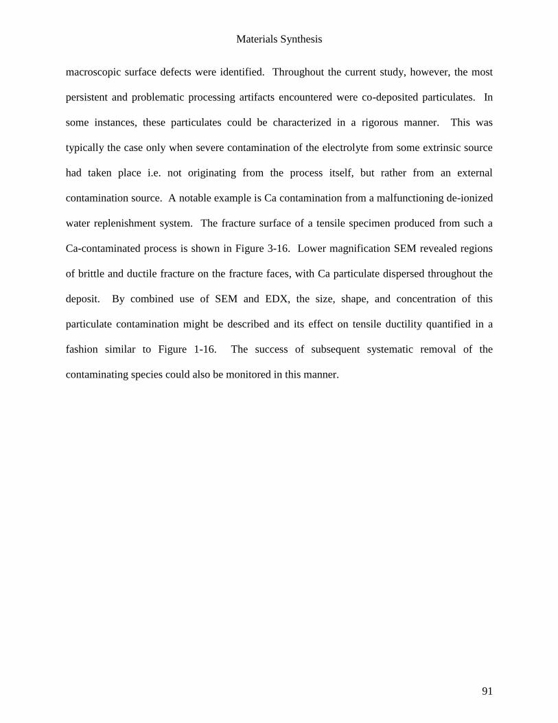
Materials Synthesis
91
macroscopic surface defects were identified. Throughout the current study, however, the most
persistent and problematic processing artifacts encountered were co-deposited particulates. In
some instances, these particulates could be characterized in a rigorous manner. This was
typically the case only when severe contamination of the electrolyte from some extrinsic source
had taken place i.e. not originating from the process itself, but rather from an external
contamination source. A notable example is Ca contamination from a malfunctioning de-ionized
water replenishment system. The fracture surface of a tensile specimen produced from such a
Ca-contaminated process is shown in Figure 3-16. Lower magnification SEM revealed regions
of brittle and ductile fracture on the fracture faces, with Ca particulate dispersed throughout the
deposit. By combined use of SEM and EDX, the size, shape, and concentration of this
particulate contamination might be described and its effect on tensile ductility quantified in a
fashion similar to Figure 1-16. The success of subsequent systematic removal of the
contaminating species could also be monitored in this manner.
Materials Synthesis
92
The second synthesis challenge relates to the presence of not only external contamination such as
foreign particulate matter but unavoidable contamination resulting from the process itself.
Consumable pure Ni “R-rounds” from INCO were used as anodes throughout this work. Over
the course of a lengthy (greater than approximately 8hrs) electroforming run, the continuous
oxidation of the Ni anode is accompanied by physical breakdown of its surface, resulting in fine
Ni particulate contamination of the electroforming bath. This is the main reason most anode
Figure 3-16 (a,b) SEM Analysis of the fracture face of a nanocrystalline Ni tensile specimen
synthesized using an electroforming process replenished with water from a malfunctioning de-
ionized water system indicating the presence of particulate contamination; (c) EDX spot
analysis of the Ca particulate (images courtesy of Peter Lin, Integran Technologies Inc.).
a) b)
c)
Materials Synthesis
93
baskets are bagged in industrial electroplating and electroforming. Metal hydroxides are also
known to form on the surface of electroplating anodes and these represent another possible
particulate contamination source. Regardless of its origin, any solution-borne particulate may
become entrapped in the electroform, causing defects similar in character to the nodule in Figure
3-15. Because particulate originating from the continuously corroding consumable Ni anode
material was chemically identical to the matrix material being reduced on the cathode surface,
the co-deposited particulate could not be resolved by conventional EDX or Back-Scattered
Electron Diffraction (BSED) techniques as per Figure 3-16. Moreover, no co-deposited nano-
sized particles originating from the anodes were ever detected on the fracture surfaces of the
subsequent tensile test specimens. In fact, to the best of the author‟s knowledge, there exist no
conventional methods or previous studies that have rigorously characterized electroforming
anode particulate contamination and its effect on material properties. Thus, the rigorous
characterization of the particulate matter of primary interest to the current study was not
possible.
A number of practical strategies to combat the issue of internally-generated particulate
contamination were nevertheless evaluated and the failures will not be described in detail here.
However, the most effective method to prevent co-deposition of the anode particulate within the
cathode plate was found to be a combination of proper tank enclosure, anode bagging (filter bag
encapsulating the anode basket), continuous electrolyte filtration, and solution flow pattern
control. This was largely an empirical exercise, with the dependent variables being macroscopic
plate defect inspection and, more rigorously, testing of multiple tensile samples cut from each
plate. In other words, for the specific case of second phase particulate chemically identical to the
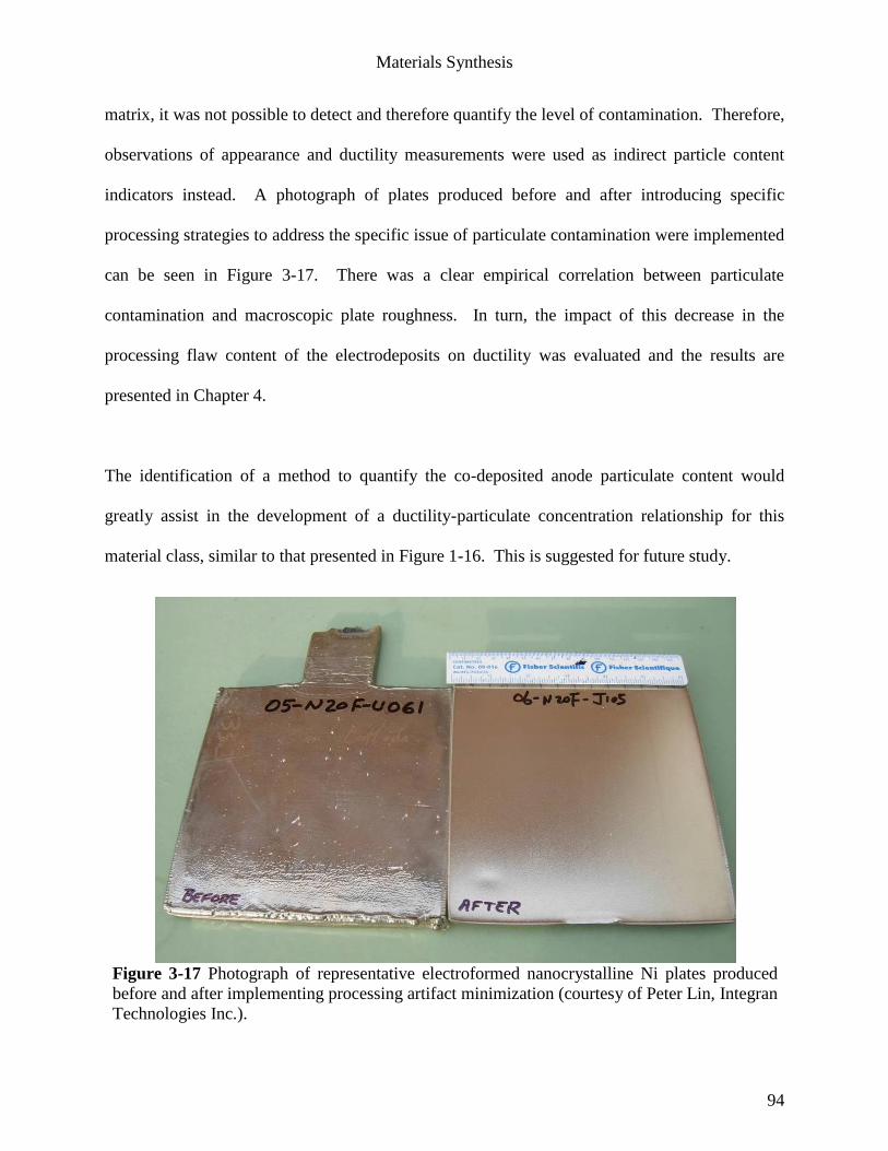
Materials Synthesis
94
matrix, it was not possible to detect and therefore quantify the level of contamination. Therefore,
observations of appearance and ductility measurements were used as indirect particle content
indicators instead. A photograph of plates produced before and after introducing specific
processing strategies to address the specific issue of particulate contamination were implemented
can be seen in Figure 3-17. There was a clear empirical correlation between particulate
contamination and macroscopic plate roughness. In turn, the impact of this decrease in the
processing flaw content of the electrodeposits on ductility was evaluated and the results are
presented in Chapter 4.
The identification of a method to quantify the co-deposited anode particulate content would
greatly assist in the development of a ductility-particulate concentration relationship for this
material class, similar to that presented in Figure 1-16. This is suggested for future study.
Figure 3-17 Photograph of representative electroformed nanocrystalline Ni plates produced
before and after implementing processing artifact minimization (courtesy of Peter Lin, Integran
Technologies Inc.).
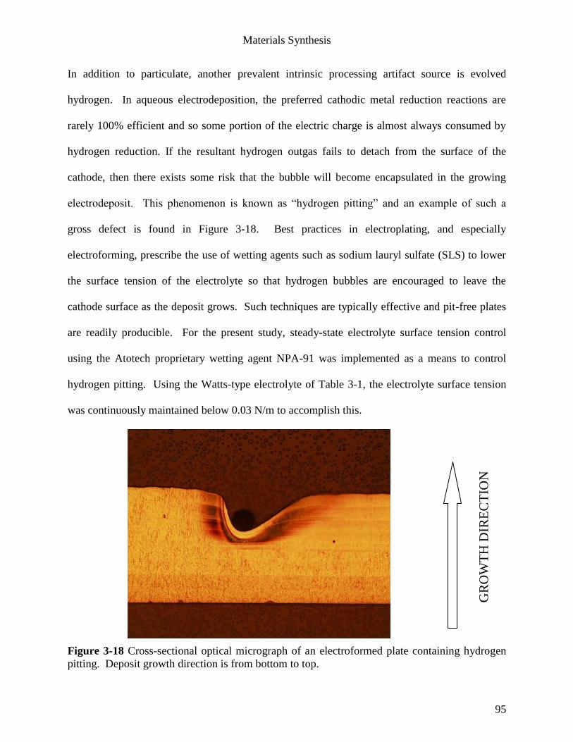
Materials Synthesis
95
In addition to particulate, another prevalent intrinsic processing artifact source is evolved
hydrogen. In aqueous electrodeposition, the preferred cathodic metal reduction reactions are
rarely 100% efficient and so some portion of the electric charge is almost always consumed by
hydrogen reduction. If the resultant hydrogen outgas fails to detach from the surface of the
cathode, then there exists some risk that the bubble will become encapsulated in the growing
electrodeposit. This phenomenon is known as “hydrogen pitting” and an example of such a
gross defect is found in Figure 3-18. Best practices in electroplating, and especially
electroforming, prescribe the use of wetting agents such as sodium lauryl sulfate (SLS) to lower
the surface tension of the electrolyte so that hydrogen bubbles are encouraged to leave the
cathode surface as the deposit grows. Such techniques are typically effective and pit-free plates
are readily producible. For the present study, steady-state electrolyte surface tension control
using the Atotech proprietary wetting agent NPA-91 was implemented as a means to control
hydrogen pitting. Using the Watts-type electrolyte of Table 3-1, the electrolyte surface tension
was continuously maintained below 0.03 N/m to accomplish this.
GR
OW
TH
DIR
EC
TIO
N
Figure 3-18 Cross-sectional optical micrograph of an electroformed plate containing hydrogen
pitting. Deposit growth direction is from bottom to top.
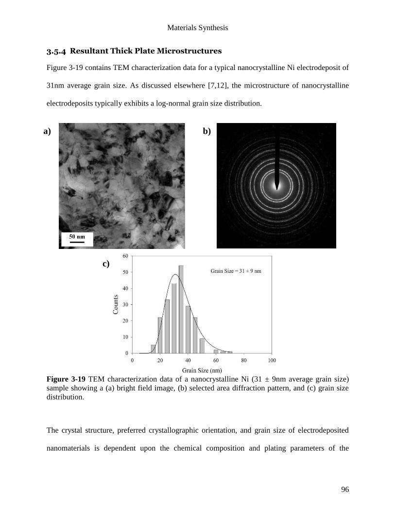
Materials Synthesis
96
3.5.4 Resultant Thick Plate Microstructures
Figure 3-19 contains TEM characterization data for a typical nanocrystalline Ni electrodeposit of
31nm average grain size. As discussed elsewhere [7,12], the microstructure of nanocrystalline
electrodeposits typically exhibits a log-normal grain size distribution.
Figure 3-19 TEM characterization data of a nanocrystalline Ni (31 ± 9nm average grain size)
sample showing a (a) bright field image, (b) selected area diffraction pattern, and (c) grain size
distribution.
The crystal structure, preferred crystallographic orientation, and grain size of electrodeposited
nanomaterials is dependent upon the chemical composition and plating parameters of the
a) b)
c)
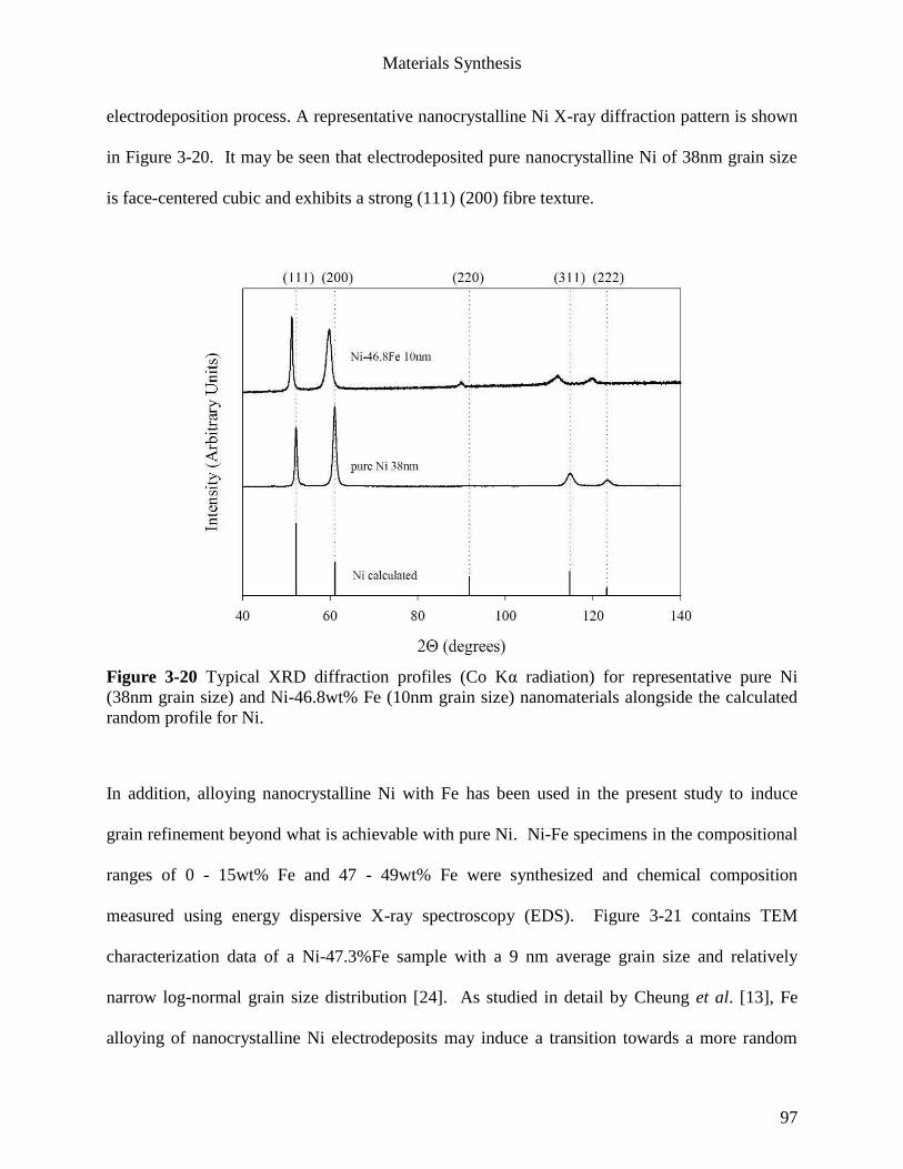
Materials Synthesis
97
electrodeposition process. A representative nanocrystalline Ni X-ray diffraction pattern is shown
in Figure 3-20. It may be seen that electrodeposited pure nanocrystalline Ni of 38nm grain size
is face-centered cubic and exhibits a strong (111) (200) fibre texture.
Figure 3-20 Typical XRD diffraction profiles (Co Kα radiation) for representative pure Ni
(38nm grain size) and Ni-46.8wt% Fe (10nm grain size) nanomaterials alongside the calculated
random profile for Ni.
In addition, alloying nanocrystalline Ni with Fe has been used in the present study to induce
grain refinement beyond what is achievable with pure Ni. Ni-Fe specimens in the compositional
ranges of 0 - 15wt% Fe and 47 - 49wt% Fe were synthesized and chemical composition
measured using energy dispersive X-ray spectroscopy (EDS). Figure 3-21 contains TEM
characterization data of a Ni-47.3%Fe sample with a 9 nm average grain size and relatively
narrow log-normal grain size distribution [24]. As studied in detail by Cheung et al. [13], Fe
alloying of nanocrystalline Ni electrodeposits may induce a transition towards a more random
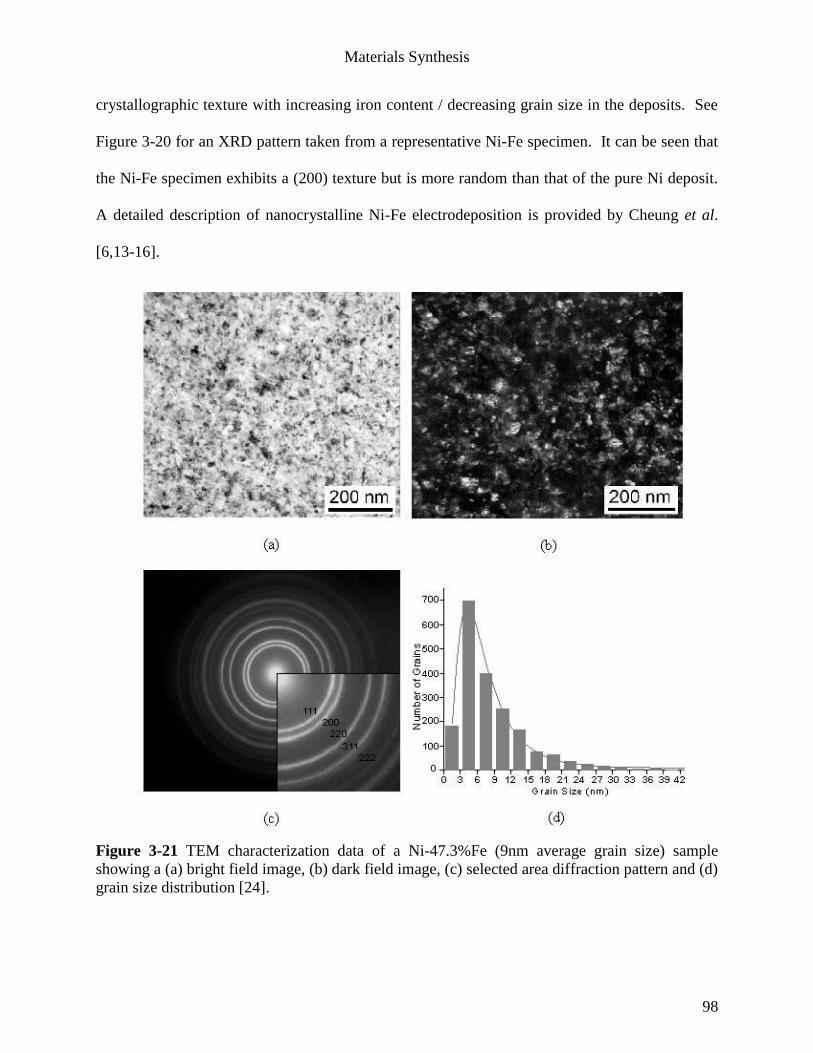
Materials Synthesis
98
crystallographic texture with increasing iron content / decreasing grain size in the deposits. See
Figure 3-20 for an XRD pattern taken from a representative Ni-Fe specimen. It can be seen that
the Ni-Fe specimen exhibits a (200) texture but is more random than that of the pure Ni deposit.
A detailed description of nanocrystalline Ni-Fe electrodeposition is provided by Cheung et al.
[6,13-16].
Figure 3-21 TEM characterization data of a Ni-47.3%Fe (9nm average grain size) sample
showing a (a) bright field image, (b) dark field image, (c) selected area diffraction pattern and (d)
grain size distribution [24].
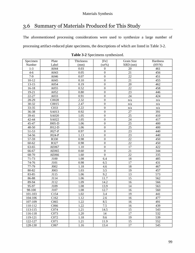
Materials Synthesis
99
3.6 Summary of Materials Produced for This Study
The aforementioned processing considerations were used to synthesize a large number of
processing artifact-reduced plate specimens, the descriptions of which are listed in Table 3-2.
Table 3-2 Specimens synthesized.
Specimen Plate Thickness [Fe] Grain Size Hardness
Number Label (mm) (wt%) XRD (nm) (HVN)
1-3 A044 0.03 0 20 461
4-6 A043 0.05 0 21 456
7-9 A046 0.07 0 22 451
10-12 A045 0.10 0 21 455
13-15 A054 0.19 0 20 462
16-18 A055 0.52 0 22 458
19-21 A052 0.80 0 23 446
22-27 A033 0.91 0 24 424
28-29 C0028 2.32 0 n/a n/a
30-32 C0015 2.47 0 n/a n/a
33-35 C033 2.22 0 n/a n/a
36-38 SA013 0.92 0 27 391
39-41 SA020 1.05 0 25 410
42-44 SA022 1.05 0 24 417
45-47 J005-D 1.06 0 25 400
48-50 J012-D 1.06 0 25 400
51-53 J027-P 0.97 0 23 440
54-56 J024-P 1.13 0 23 440
57-59 R330 0.98 0 22 450
60-62 R327 0.98 0 22 450
63-65 AE067 1.10 0 17 422
66-67 AE065 0.60 0 21 344
68-70 AE066 1.60 0 22 335
71-73 J100 1.08 6.4 18 485
74-76 J101 0.98 6.5 17 431
77-79 J002 1.18 4.6 18 467
80-82 J003 1.03 3.5 19 457
83-85 J115 1.06 9.2 13 573
86-88 J114 1.06 11.7 15 562
89-94 J112 1.09 14.2 16 566
95-97 J109 1.08 13.9 14 563
98-100 J107 1.08 12.7 16 560
101-103 C154 1.02 3.4 19 441
104-106 C162 1.12 2.6 16 477
107-109 C065 1.22 8.5 16 491
110-112 C066 1.22 7.5 16 439
113-115 C074 1.21 14.5 15 543
116-118 C073 1.20 14 17 532
119-121 C072 1.18 9.6 19 539
122-127 C071 1.21 11.9 15 552
128-130 C067 1.16 13.4 17 545
Materials Synthesis
100
131-134 B3R2 0.60 6.3 23 n/a
135-137 B2R6 0.89 7.6 18 522
138-140 B2R3 0.78 6.2 18 n/a
141-143 B2R8 2.27 5.5 18 497
144-146 J023 1.07 45.1 11 528
147-149 J022 1.05 47.4 12 526
150-152 J021 1.06 46.8 12 513
153-158 J019 1.06 46.8 13 479
159-161 J016 1.00 46.4 13 485
It should be noted that there exists general consistency between the XRD-based grain size values
and those based upon application of the Hall-Petch relationship to the measured hardness values
listed in Table 3-2 with one notable exception. Specimens 66-70 cut from plates labeled AE065
and AE066 exhibited XRD peak broadening that resulted in calculated average grain size values
of 21 and 22nm, respectively. However, the hardness and strength properties of these specimens
were indicative of a much coarser microstructure. For example, the average hardness and yield
strength values of the two samples cut from plate AE065 were only 344 VHN and 702 MPa,
respectively, values that would be expected from Ni with a grain size much larger than 21nm. In
order to explain this unexpected result, TEM analysis was performed on specimen AE065 and a
representative bright field image is presented in Figure 3-22. It was found that the average grain
size of this specimen was 80nm and that the material exhibited an unexpectedly large
concentration of faulted regions and microtwins. These faulted regions are likely the origin of
the anomalously high XRD peak broadening upon which the 21nm grain size calculation was
based. From a synthesis perspective, the origin of this microstructure is unknown.
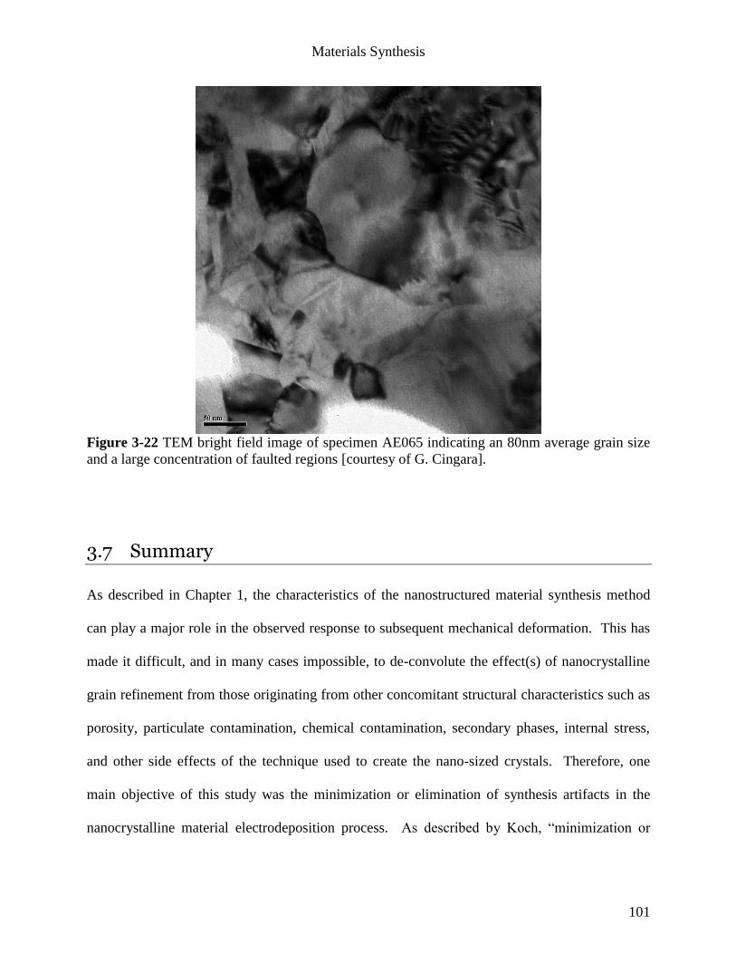
Materials Synthesis
101
Figure 3-22 TEM bright field image of specimen AE065 indicating an 80nm average grain size
and a large concentration of faulted regions [courtesy of G. Cingara].
3.7 Summary
As described in Chapter 1, the characteristics of the nanostructured material synthesis method
can play a major role in the observed response to subsequent mechanical deformation. This has
made it difficult, and in many cases impossible, to de-convolute the effect(s) of nanocrystalline
grain refinement from those originating from other concomitant structural characteristics such as
porosity, particulate contamination, chemical contamination, secondary phases, internal stress,
and other side effects of the technique used to create the nano-sized crystals. Therefore, one
main objective of this study was the minimization or elimination of synthesis artifacts in the
nanocrystalline material electrodeposition process. As described by Koch, “minimization or
Materials Synthesis
102
elimination of processing artifacts is the key to revealing the inherent mechanical properties of
nanocrystalline materials and potentially optimizing high strength and good ductility” [25]. In
this chapter, it was demonstrated that electroformed specimens substantially reduced in defects
such as hydrogen pitting, chemical contamination, and particulate contamination could be
reproducibly synthesized through adoption of specific strategies such as steady state chemical
control, fine particulate filtering, improved feedstock chemical quality, and so on. As will be
described in Chapter 4, the “quality” criteria throughout this work were macroscopic plate defect
inspection and, more rigorously, achievable tensile elongation-to-fracture of multiple samples cut
from each individual plate produced. In other words, it was found that artifact-reduced
specimens were more ductile and showed less sample-to-sample variability in elongation-to-
fracture than specimens produced from a defect-rich process. Owing to the inability to
rigorously characterize the artifacts themselves due to the identical chemical character of the
matrix and second phase particles in question, these strain-to-fracture tests effectively served as
indirect measurements of the co-deposited material particle content.
The second objective of this study was to answer the question of whether it is possible to
synthesize bulk quantities of electrodeposited nanocrystalline materials to enable tensile testing
in conformance with ASTM E8 since, prior to this study, reproducible nanomaterials thick plate
electroforming had not been possible. It was found that processing artifact minimization and
electrodeposit internal stress control enabled the systematic production of a large number of
artifact-free 152mm x 152 mm plates of 1mm thickness and beyond.
Materials Synthesis
103
3.8 References
[1] R. Parkinson, Electroforming – A unique metal fabrication process, NDI Technical Series,
No. 10085, Toronto, ON (2001).
[2] U. Erb et al., in Nanostructured Metals and Alloys, S.H. Whang (ed.), Woodhead Publ.,
Oxford, UK (2011) 118.
[3] J. Matulis R. Slizys, Electrochim. Acta, 9 (1964) 1177.
[4] R.C.V. Piatti, A.J. Arvia, J.J. Podesta, Electrochim. Acta, 14 (1969) 541.
[5] U. Erb, A.M. El-Sherik, US Patent #5,352,266 (1994).
[6] U. Erb, A.M. El-Sherik, C.K.S. Cheung, M.J. Aus, US Patent #5,433,797 (1995).
[7] G. McMahon, U. Erb, Microstr. Sci. 17 (1989) 447.
[8] C. Chan, M.Sc. Thesis, University of Toronto (2011).
[9] G. Gunawardena, G. Hills, I. Montenegro, B. Scharifker, J. Electroanal. Chem. 138 (1982)
255.
[10] R.T.C. Choo, A.M. El-Sherik, J. Toguri, U. Erb, J. Appl. Electrochem., 25 (1995) 384.
[11] U. Erb, in Nanostructured Materials: Processing, Properties and Applications, 2nd
ed., C.C.
Koch (ed.), William Andrew Pub., Norwich, NY (2007) 239.
[12] A.M. El-Sherik, U. Erb, J. Mater. Sci. 30 (1995) 5743.
[13] C. Cheung, F. Djuanda, U. Erb, G. Palumbo, Nanostr. Mater., 5, 5 (1995) 513.
[14] C.K.S. Cheung, Ph.D. Thesis, Queen‟s University (2001).
[15] C. Cheung, G. Palumbo, U. Erb, Scripta Metall. Mater. 31,6 (1994) 735.
[16] C. Cheung, P. Nolan, U. Erb, Mater. Lett., 20 (1994) 135.
[17] R. Weil, K. Sheppard, Mater. Char., 28 (1992) 103.
Materials Synthesis
104
[18] B. Stein, in AESF SUR/FIN Tech. Proc., Las Vegas, NV, American Electroplaters and
Surface Finishers (1996).
[19] R. Parkinson, in Electroforming Course and Symposium, Nickel Development Institute /
American Electroplaters and Surface Finishers Society, San Diego, CA (1997).
[20] J.W. Dini, Electrodeposition: The Materials Science of Coatings and Substrates, Noyes
Pub., Park Ridge, NJ (1993).
[21] A. Stukowski, J. Markmann, J. Weissmuller, K. Albe, Acta Mater., 57, 5 (2009) 1648.
[22] J. Giallonardo, Ph.D. Thesis, University of Toronto
[23] M. Schlesinger, in Modern Electroplating, 4th
ed., eds. M. Schlesinger, M. Paunovic, John
Wiley and Sons, New York NY (2000) 35.
[24] H. Wei, M.A.Sc. thesis, University of Toronto (2006).
[25] Koch CC in: Structural Nanocrystalline Materials, (C.C. Koch et al. (eds)), Cambridge
University Press, Cambridge, UK (2007) 134.
105
Chapter 4 Ductility
The key findings contained in this chapter were previously presented in the following refereed
article: I. Brooks, G. Palumbo, G.D. Hibbard, Zhirui Wang, U. Erb, "On the Intrinsic Ductility
of Electrodeposited Nanocrystalline Metals", Journal of Materials Science 46 (2011) 7713.
4.1 Introduction
While much has been written concerning the relationship between grain size and strength [e.g. 1-
3] and hardness [e.g. 4-6], the literature contains a great deal of conflicting data regarding the
intrinsic ductility and toughness of nanocrystalline materials [e.g. 7-9]. Ductility is defined as
the ability of a material to undergo plastic deformation without fracture [10] and is not only a
key piece of information that must be considered in material formability considerations and the
design of reliable load bearing structures, but is also a very useful measure in the broader
assessment of material quality and damage tolerance. In the case of nanocrystalline materials,
there are a number of factors that have contributed to a lack of clarity on the topic, as will be
discussed below. It is the goal of this chapter to elucidate some of the causes of past ambiguity
and to employ data gathered using a very large set of electrodeposited nanocrystalline material
specimens to study the intrinsic ductility of this important material class.
4.2 Experimental Details
4.2.1 Material Synthesis and Characterization
As discussed in Chapter 3, the nature of electrodeposition is such that electrodeposited materials
typically contain various types of inclusions and/or impurities, and one primary objective of the
Ductility
106
materials synthesis component of this thesis was the minimization of processing artifacts such as
hydrogen pits, nodular deposit growth and co-deposited fine particulate matter in the production
of bulk, thick plate specimens for testing in conformance with ASTM E8 [11]. This was largely
an empirical exercise, with the dependent variables being macroscopic plate defect inspection
and, more rigorously, testing of multiple tensile samples cut from each plate.
4.2.2 Mechanical Testing
As described in Chapter 2, all samples were tested to fracture using a calibrated load cell and the
elongation to fracture, εf, was measured using both a calibrated extensometer and also by
measurement of the gauge length before and after testing. The peak load method was used to
designate the onset of plastic instability in order to determine the maximum uniform elongation.
The elastic component of the maximum uniform strain was assumed to be equivalent to the strain
measured from the onset of loading until the 0.2% offset yield point [11] with elastic strain
values typically falling within the range of 0.5 to 1%. The difference between the measured
maximum uniform strain (at peak load) and the elastic strain term was then termed the maximum
uniform plastic strain.
4.2.3 Data Analysis
Two-parameter Weibull distributional analysis was used to quantify the variability in the
ductility data. Weibull analysis is one of the most commonly used tools in reliability analysis,
and is based upon a probabilistic “weakest link” depiction of the scatter in the time-to-failure of
engineering components. Its basic assumptions are the existence of statistically distributed
defects throughout the volume and on the surfaces of the material and that the structure can be
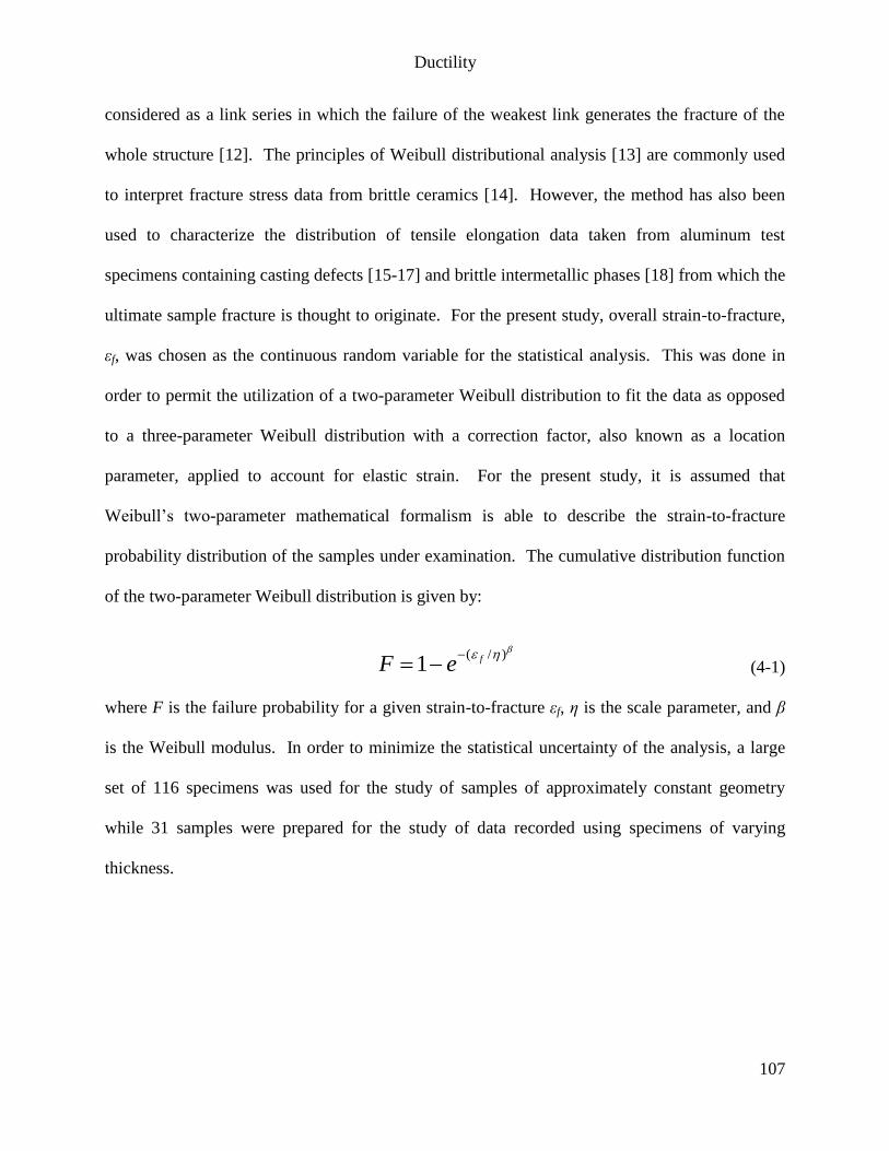
Ductility
107
considered as a link series in which the failure of the weakest link generates the fracture of the
whole structure [12]. The principles of Weibull distributional analysis [13] are commonly used
to interpret fracture stress data from brittle ceramics [14]. However, the method has also been
used to characterize the distribution of tensile elongation data taken from aluminum test
specimens containing casting defects [15-17] and brittle intermetallic phases [18] from which the
ultimate sample fracture is thought to originate. For the present study, overall strain-to-fracture,
εf, was chosen as the continuous random variable for the statistical analysis. This was done in
order to permit the utilization of a two-parameter Weibull distribution to fit the data as opposed
to a three-parameter Weibull distribution with a correction factor, also known as a location
parameter, applied to account for elastic strain. For the present study, it is assumed that
Weibull’s two-parameter mathematical formalism is able to describe the strain-to-fracture
probability distribution of the samples under examination. The cumulative distribution function
of the two-parameter Weibull distribution is given by:
)/(1 feF
(4-1)
where F is the failure probability for a given strain-to-fracture εf, η is the scale parameter, and β
is the Weibull modulus. In order to minimize the statistical uncertainty of the analysis, a large
set of 116 specimens was used for the study of samples of approximately constant geometry
while 31 samples were prepared for the study of data recorded using specimens of varying
thickness.
Ductility
108
4.3 Results and Discussion
The first problem addressed in Section 4.3.1 is the effect of processing artifacts on tensile
ductility. A largely empirical process of artifact minimization was then performed, and a
material synthesis protocol was established that was as consistent and artifact-free as possible
with the quality control parameter throughout being tensile tests of multiple samples cut from a
single plate. Once a consistent sample-to-sample tensile elongation value that exceeded the
onset of tensile necking instability was achieved, all relevant process parameters were locked in
place and strictly controlled for every subsequent plate produced. The first study thereafter
focused upon the effect of tensile specimen thickness on elongation measurements, and the
results of this work comprise Section 4.3.2 of this chapter. Finally, to eliminate the geometry
effect from further consideration and to explore the statistical variability in intrinsic achievable
tensile elongation, a statistically significant number of 116 specimens of fixed sample thickness
cut from relatively thick (approximately 1mm) monolithic nanocrystalline Ni-based
electrodeposits produced using a well-controlled, steady state electroforming process were then
evaluated and the results are discussed in Section 4.3.3.
4.3.1 Effect of Processing Artifacts
Since ductility as measured by strain-to-fracture in quasi-static tensile extension of a typical high
strength material is strongly influenced by the propagation of pre-existing flaws in the sample,
the electrodeposition processing parameters used to fabricate the nanocrystalline material play a
key role because they typically dictate the type, size, orientation, and concentration of processing
artifacts that are created as the material is formed. As discussed in Chapter 3, the processing
parameters that enable the reduction of gross macroscopic defects were identified as part of this
Ductility
109
study. The most persistent and problematic processing artifacts encountered throughout this
work were co-deposited particulates. A photograph of plates produced before and after
processing strategies to address the specific issue of particulate contamination were implemented
was presented in Figure 3-17. There was a clear empirical correlation between particulate
contamination and macroscopic plate roughness.
The correlation between macroscopic plate roughness and co-deposited particulate content was
also found to extend to specimen ductility. In order to quantify this effect, tensile tests were
performed. Figure 4-1(a) contains tensile engineering stress-strain curves corresponding to six
individual tensile bars cut from a single nanocrystalline Ni plate produced using an early scale-
up stage electroforming process alongside data gathered from an otherwise identical plate
produced using the later generation process with much stricter processing artifact control (Figure
4-1(b)).
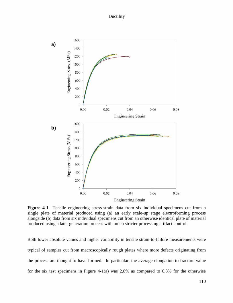
Ductility
110
Both lower absolute values and higher variability in tensile strain-to-failure measurements were
typical of samples cut from macroscopically rough plates where more defects originating from
the process are thought to have formed. In particular, the average elongation-to-fracture value
for the six test specimens in Figure 4-1(a) was 2.8% as compared to 6.8% for the otherwise
Figure 4-1 Tensile engineering stress-strain data from six individual specimens cut from a
single plate of material produced using (a) an early scale-up stage electroforming process
alongside (b) data from six individual specimens cut from an otherwise identical plate of material
produced using a later generation process with much stricter processing artifact control.
A C
B
a)
b)
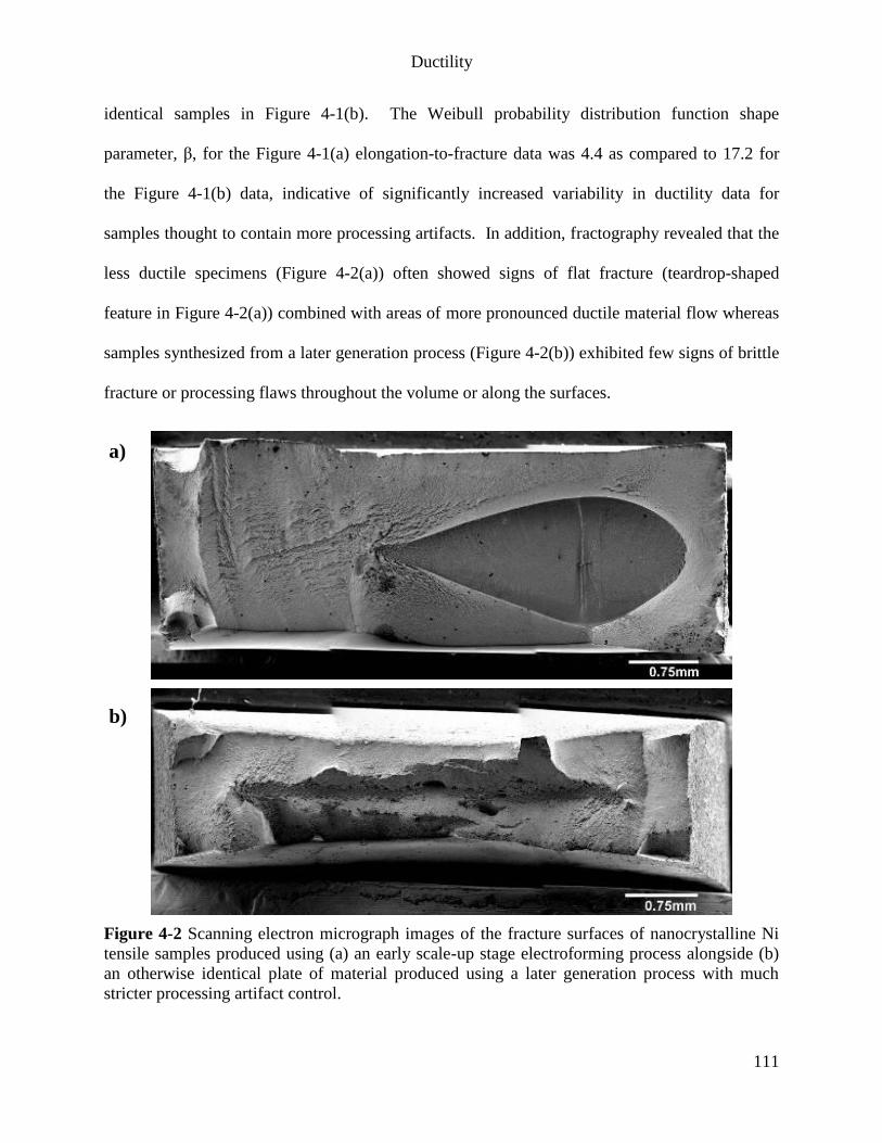
Ductility
111
identical samples in Figure 4-1(b). The Weibull probability distribution function shape
parameter, β, for the Figure 4-1(a) elongation-to-fracture data was 4.4 as compared to 17.2 for
the Figure 4-1(b) data, indicative of significantly increased variability in ductility data for
samples thought to contain more processing artifacts. In addition, fractography revealed that the
less ductile specimens (Figure 4-2(a)) often showed signs of flat fracture (teardrop-shaped
feature in Figure 4-2(a)) combined with areas of more pronounced ductile material flow whereas
samples synthesized from a later generation process (Figure 4-2(b)) exhibited few signs of brittle
fracture or processing flaws throughout the volume or along the surfaces.
Figure 4-2 Scanning electron micrograph images of the fracture surfaces of nanocrystalline Ni
tensile samples produced using (a) an early scale-up stage electroforming process alongside (b)
an otherwise identical plate of material produced using a later generation process with much
stricter processing artifact control.
a)
b)
Ductility
112
It is unreasonable to expect that the electroforming process improvements developed as part of
this study were successful in completely eliminating all processing artifacts. However, the fact
that all thick, artifact-reduced samples were intrinsically ductile enough to surpass a point of
peak load indicates that the processing artifact content was sufficiently low for final fracture to
be initiated by plastic instability. Past the onset of plastic necking instability at the ultimate
tensile stress point, it is very likely the case that further improvements in processing artifact
control might yield increased elongation before fracture, as will be discussed in more detail in
the following section. However, for the purposes of the current study, once a consistent sample-
to-sample tensile elongation value that exceeded the onset of tensile necking instability was
achieved, all relevant process parameters were locked in place and strictly controlled for every
subsequent plate produced. All specimens produced for the subsequent sections of this chapter
were substantially free of major electroforming artifacts such as large hydrogen pit holes,
localized dendritic growth, and other prominent surface and volume flaws.
4.3.2 Effect of Sample Geometry
Figure 4-3 shows the relationship between specimen thickness and total achievable strain-to-
fracture (based upon measurement of the gauge length before and after tensile testing) for 31
nanocrystalline Ni specimens of varying thickness processed in an identical fashion in order to
yield similar microstructures and processing defect contents. In other words, the sole processing
difference between the specimens from which the Figure 4-3 data originates is that the thicker
plates were electrodeposited for a longer duration than the thinner ones.
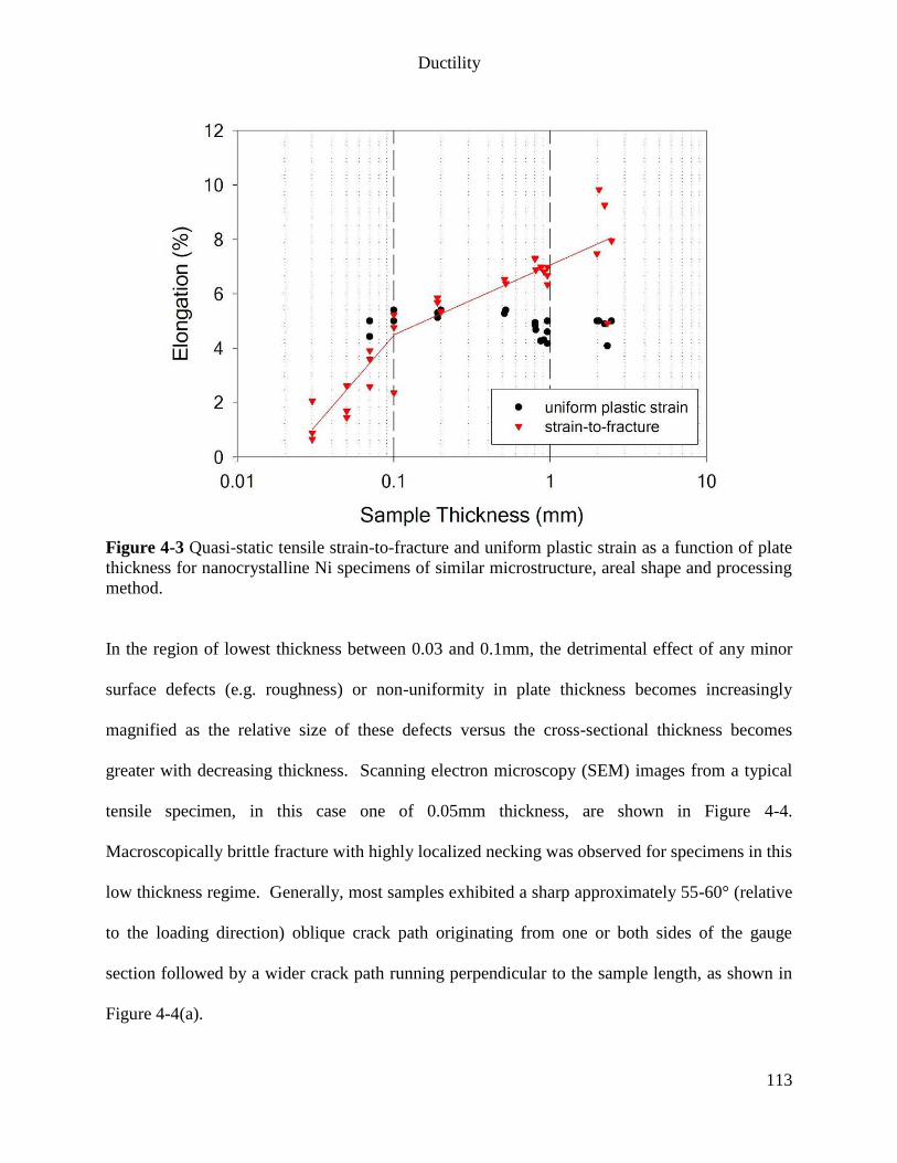
Ductility
113
Figure 4-3 Quasi-static tensile strain-to-fracture and uniform plastic strain as a function of plate
thickness for nanocrystalline Ni specimens of similar microstructure, areal shape and processing
method.
In the region of lowest thickness between 0.03 and 0.1mm, the detrimental effect of any minor
surface defects (e.g. roughness) or non-uniformity in plate thickness becomes increasingly
magnified as the relative size of these defects versus the cross-sectional thickness becomes
greater with decreasing thickness. Scanning electron microscopy (SEM) images from a typical
tensile specimen, in this case one of 0.05mm thickness, are shown in Figure 4-4.
Macroscopically brittle fracture with highly localized necking was observed for specimens in this
low thickness regime. Generally, most samples exhibited a sharp approximately 55-60° (relative
to the loading direction) oblique crack path originating from one or both sides of the gauge
section followed by a wider crack path running perpendicular to the sample length, as shown in
Figure 4-4(a).
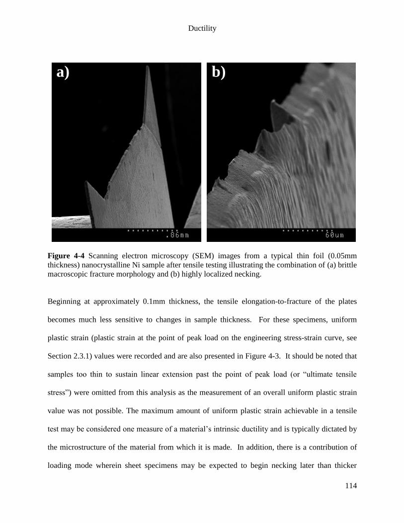
Ductility
114
Beginning at approximately 0.1mm thickness, the tensile elongation-to-fracture of the plates
becomes much less sensitive to changes in sample thickness. For these specimens, uniform
plastic strain (plastic strain at the point of peak load on the engineering stress-strain curve, see
Section 2.3.1) values were recorded and are also presented in Figure 4-3. It should be noted that
samples too thin to sustain linear extension past the point of peak load (or “ultimate tensile
stress”) were omitted from this analysis as the measurement of an overall uniform plastic strain
value was not possible. The maximum amount of uniform plastic strain achievable in a tensile
test may be considered one measure of a material’s intrinsic ductility and is typically dictated by
the microstructure of the material from which it is made. In addition, there is a contribution of
loading mode wherein sheet specimens may be expected to begin necking later than thicker
Figure 4-4 Scanning electron microscopy (SEM) images from a typical thin foil (0.05mm
thickness) nanocrystalline Ni sample after tensile testing illustrating the combination of (a) brittle
macroscopic fracture morphology and (b) highly localized necking.
a) b)
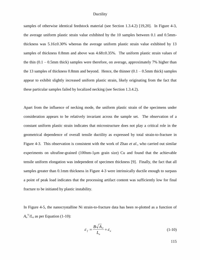
Ductility
115
samples of otherwise identical feedstock material (see Section 1.3.4.2) [19,20]. In Figure 4-3,
the average uniform plastic strain value exhibited by the 10 samples between 0.1 and 0.5mm-
thickness was 5.16±0.30% whereas the average uniform plastic strain value exhibited by 13
samples of thickness 0.8mm and above was 4.68±0.35%. The uniform plastic strain values of
the thin (0.1 – 0.5mm thick) samples were therefore, on average, approximately 7% higher than
the 13 samples of thickness 0.8mm and beyond. Hence, the thinner (0.1 – 0.5mm thick) samples
appear to exhibit slightly increased uniform plastic strain, likely originating from the fact that
these particular samples failed by localized necking (see Section 1.3.4.2).
Apart from the influence of necking mode, the uniform plastic strain of the specimens under
consideration appears to be relatively invariant across the sample set. The observation of a
constant uniform plastic strain indicates that microstructure does not play a critical role in the
geometrical dependence of overall tensile ductility as expressed by total strain-to-fracture in
Figure 4-3. This observation is consistent with the work of Zhao et al., who carried out similar
experiments on ultrafine-grained (100nm-1µm grain size) Cu and found that the achievable
tensile uniform elongation was independent of specimen thickness [9]. Finally, the fact that all
samples greater than 0.1mm thickness in Figure 4-3 were intrinsically ductile enough to surpass
a point of peak load indicates that the processing artifact content was sufficiently low for final
fracture to be initiated by plastic instability.
In Figure 4-5, the nanocrystalline Ni strain-to-fracture data has been re-plotted as a function of
Ao½/Lo as per Equation (1-10):
u
o
o
fL
AB (1-10)
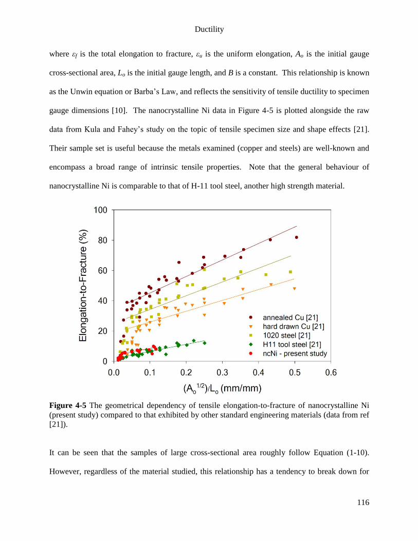
Ductility
116
where εf is the total elongation to fracture, εu is the uniform elongation, Ao is the initial gauge
cross-sectional area, Lo is the initial gauge length, and B is a constant. This relationship is known
as the Unwin equation or Barba’s Law, and reflects the sensitivity of tensile ductility to specimen
gauge dimensions [10]. The nanocrystalline Ni data in Figure 4-5 is plotted alongside the raw
data from Kula and Fahey’s study on the topic of tensile specimen size and shape effects [21].
Their sample set is useful because the metals examined (copper and steels) are well-known and
encompass a broad range of intrinsic tensile properties. Note that the general behaviour of
nanocrystalline Ni is comparable to that of H-11 tool steel, another high strength material.
Figure 4-5 The geometrical dependency of tensile elongation-to-fracture of nanocrystalline Ni
(present study) compared to that exhibited by other standard engineering materials (data from ref
[21]).
It can be seen that the samples of large cross-sectional area roughly follow Equation (1-10).
However, regardless of the material studied, this relationship has a tendency to break down for
Ductility
117
smaller samples of cross-sectional area below approximately 2 mm2, or 0.04 mm/mm (Ao
½/Lo) on
Figure 4-5. The observations of the present study are consistent with those of Kula and Fahey
and indicate that regardless of the intrinsic ductility of the material under examination, the
achievable tensile elongation-to-fracture of thin tensile samples is inherently less predictable as
neck development becomes increasingly geometry/surface-flaw sensitive with decreasing
thickness.
The relationship between total elongation-to-fracture and sample geometry of the nanocrystalline
Ni samples was also observed to become more unpredictable at the other end of the thickness
spectrum (>2mm, Figure 4-3), this time in contrast to the behaviour of the conventional
engineering material benchmarks. Of the five nanocrystalline Ni samples from the highest
thickness (>2mm) regime, four exhibited signs of appreciable ductile material flow (εf = 7-10%),
as expected from a relatively defect-free high strength metallic engineering material, while the
fifth fractured soon after the onset of post-uniform elongation (indicative of the presence of
critical defects). This indicates that, in the case of the thickest nanocrystalline Ni plates, the
probability of encountering a critical “ductility controlling” volume defect may become less
predictable, and possibly even increase, with increasing plate thickness. On the other hand, it is
reasonable to assume that the type, size, orientation and concentration of flaws distributed
throughout the volume of the Figure 4-5 benchmark engineering material specimens is relatively
constant across the entire sample set because all specimens were taken from a common piece of
bar stock material prepared by conventional metallurgical means, with individual tensile samples
sliced to the desired thickness thereafter [21]. This is in contrast to the nanocrystalline
Ductility
118
specimens of varying thickness from the current study, which were not cut from a common stock
but rather deposited for varying times in the material synthesis process.
These observations invoked the use of Weibull distributional analysis to quantify the variability
in ductility data. Figure 4-6(a) contains the two-parameter Weibull plot produced using the
tensile strain-to-fracture data from the 31 sample set of nanocrystalline Ni tensile specimens of
varying thickness and Equation (4-1). Two marked transitions in slope indicate that the
geometry-dependent strain-to-fracture data regimes possess unique probability distribution
functions. In particular, the probability distribution function shape parameter of the <0.1mm-
thick nanocrystalline Ni plate strain-to-fracture values (β = 1.3) was much smaller than those in
the 0.1 – 1.25mm thickness regime (β = 5.9), indicative of a significant drop in ductility
reliability for the thinnest specimens. This is the regime where surface flaws play a key role i.e.
slant localized fracture at the expected 55° angle may not necessarily span the entire specimen
width, but rather proceed only in the initial stages of plastic deformation with brittle fracture
perpendicular to the loading direction accompanied by negligible necking proceeding thereafter,
as was shown in Figure 4-4. Here tensile plasticity is highly sensitive to specimen thickness and
is relatively unpredictable. Therefore, the practical implication is that one must design on the
basis of elastic limit for freestanding, monolithic plates of nanocrystalline Ni from this
geometrical regime when loaded in tension, with minimal capability for plastic flow to be
expected. Moreover, it can also be concluded that work to improve the mechanical reliability of
these materials should be focused primarily upon surface defects, namely improved process
control to increase the overall plate thickness uniformity over the entire sample surface and to
minimize the formation of surface asperities such as hydrogen pits, nodular deposit growth, etc.
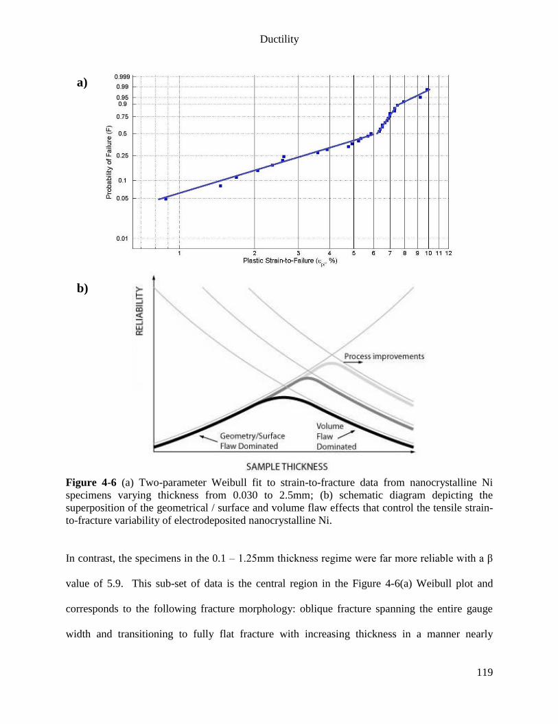
Ductility
119
In contrast, the specimens in the 0.1 – 1.25mm thickness regime were far more reliable with a β
value of 5.9. This sub-set of data is the central region in the Figure 4-6(a) Weibull plot and
corresponds to the following fracture morphology: oblique fracture spanning the entire gauge
width and transitioning to fully flat fracture with increasing thickness in a manner nearly
Figure 4-6 (a) Two-parameter Weibull fit to strain-to-fracture data from nanocrystalline Ni
specimens varying thickness from 0.030 to 2.5mm; (b) schematic diagram depicting the
superposition of the geometrical / surface and volume flaw effects that control the tensile strain-
to-fracture variability of electrodeposited nanocrystalline Ni.
b
a)
b)
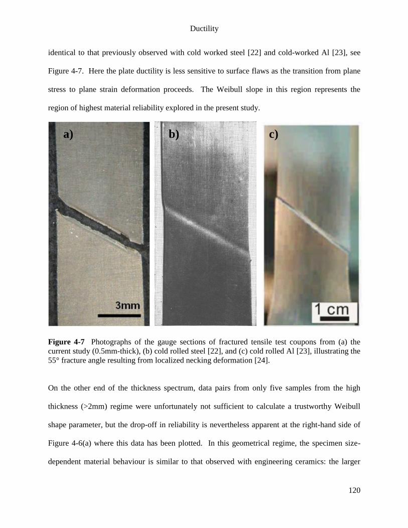
Ductility
120
identical to that previously observed with cold worked steel [22] and cold-worked Al [23], see
Figure 4-7. Here the plate ductility is less sensitive to surface flaws as the transition from plane
stress to plane strain deformation proceeds. The Weibull slope in this region represents the
region of highest material reliability explored in the present study.
Figure 4-7 Photographs of the gauge sections of fractured tensile test coupons from (a) the
current study (0.5mm-thick), (b) cold rolled steel [22], and (c) cold rolled Al [23], illustrating the
55° fracture angle resulting from localized necking deformation [24].
On the other end of the thickness spectrum, data pairs from only five samples from the high
thickness (>2mm) regime were unfortunately not sufficient to calculate a trustworthy Weibull
shape parameter, but the drop-off in reliability is nevertheless apparent at the right-hand side of
Figure 4-6(a) where this data has been plotted. In this geometrical regime, the specimen size-
dependent material behaviour is similar to that observed with engineering ceramics: the larger
a) b) c)
Ductility
121
the specimen, the greater the probability of a critical “ductility controlling” flaw, and the less
ductile it is likely to be.
This superposition of the geometrical / surface and volume flaw effects that control the
achievable tensile elongation of this electrodeposited material system is captured in schematic
form in Figure 4-6(b). Here the reliability of the tensile strain-to-fracture data has been
arbitrarily represented on the ordinate axis as a function of sample thickness. Thin samples
exhibit highly localized deformation behaviour with ultimate fracture being governed by surface
flaws and inhomogeneous plate thickness effects. The reliability increases with sample thickness
until volume artifacts associated with the electroforming process begin to dominate. One
implication of this behaviour is that the region of highest reliability in Figure 4-6(b) can very
likely be extended to much higher thickness values (with a commensurate increase in overall
achievable tensile elongation as per Equation (1-10)) via further improvements in electroforming
processing flaw elimination. In other words, it would be reasonable to expect that
nanocrystalline Ni plates with Ao½/Lo values that exceed approximately 0.04 mm/mm and
produced using a process free of gross volume defects would predictably follow a relationship of
the form of Equation (1-10). More importantly, as depicted in Figure 4-6(b), it is anticipated that
such processing improvements might also increase the overall mechanical reliability in tensile
loading, manifested in even higher Weibull shape parameters than those observed in the present
study.
In conclusion, it is apparent from an examination of Figure 4-6 that, as compared to the 0.1 –
1.25mm thickness range, one can expect much less predictability in the tensile ductility of either
Ductility
122
extremely thin monolithic plates of electrodeposited nanocrystalline Ni where the samples are
highly sensitive to the presence of surface flaws or in extremely thick (greater than
approximately 2mm) samples where the presence of critical ductility controlling volume flaws
during lengthy electroforming runs may become significantly more problematic.
Unfortunately, due to sample availability, it is difficult to better define the reliability regions on
the basis of thickness. Most notably, more samples from the 0.2 to 0.5mm and 1 to 2mm
thickness regimes would be required to do so. Nevertheless, based upon the data in-hand, it can
be concluded that if monolithic plates of nanocrystalline Ni electroformed from a process similar
to that of the present study are to be used in structural applications with tensile loading
perpendicular to the deposit growth direction, 0.1 to 1-2mm is the most reliable thickness regime
as indicated by tensile strain-to-fracture statistical variability.
Optical micrographs of representative nanocrystalline Ni samples after fracture spanning the
entire range of specimen thicknesses are shown in Figure 4-8. The thinnest samples showed
fracture along an oblique plane inclined at 55° with respect to the loading axis, gauge width
reductions of approximately 2% and gauge thickness reductions of approximately 30 to 45%
(Figure 4-8(a)). This localized necking mode was predominant for the specimens with a width-
to-thickness ratio (w/t) greater than 8 (Figures 4-8(a),(b)). On the other hand, the thicker
samples showed a transition towards diffuse necking. In particular, the specimens with a width-
to-thickness ratio less than 8 exhibited flat fracture after necking down symmetrically around the
section normal to the loading direction (Figures 4-8(c),(d)), with the thickest samples (Figures 4-
8(d)) exhibiting gauge width reductions of approximately 15% and gauge thickness reductions of
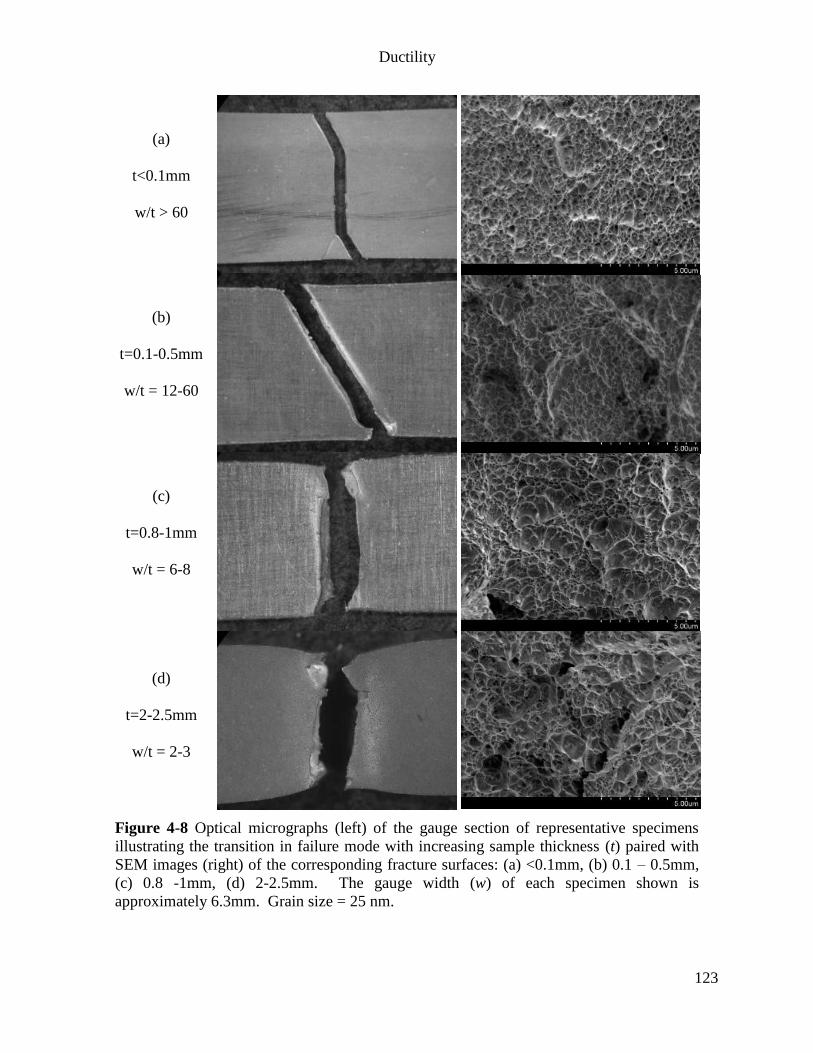
Ductility
123
(a)
t<0.1mm
w/t > 60
(b)
t=0.1-0.5mm
w/t = 12-60
(c)
t=0.8-1mm
w/t = 6-8
(d)
t=2-2.5mm
w/t = 2-3
Figure 4-8 Optical micrographs (left) of the gauge section of representative specimens
illustrating the transition in failure mode with increasing sample thickness (t) paired with
SEM images (right) of the corresponding fracture surfaces: (a) <0.1mm, (b) 0.1 – 0.5mm,
(c) 0.8 -1mm, (d) 2-2.5mm. The gauge width (w) of each specimen shown is
approximately 6.3mm. Grain size = 25 nm.
Ductility
124
approximately 30%. The samples of the present study therefore exhibited varying amounts of
localized and diffuse necking depending on the sheet thickness. These observations are
consistent with the fracture behaviour of wide, flat tensile specimens cut from cold worked steel
and Al sheet (Figure 4-7) and ultrafine-grained Cu produced by equal-channel angular pressing
[9]. As the gauge width-to-thickness ratio increases, there is increased restraint in the width
direction such that the contribution of thickness versus width strain to the measured linear
extension becomes increasingly asymmetrical and this geometrical constraint plays an important
role in the development of the neck [21]. Further commentary on the plastic instability of wide
flat tensile specimens may be found in [22,24].
Higher magnification SEM examination of the nanocrystalline Ni fracture surfaces (see Figure 4-
8, right-hand side) revealed dimpling indicative of localized ductile plastic flow for all specimens
examined, regardless of geometry. The fact that all samples studied exhibited such similar signs
of local plasticity, independent of whether the macroscopic failure mode was brittle or ductile in
appearance, supports the view that the observed dependence of overall ductility on plate
thickness is a mechanics effect associated with the size of the deformation zone relative to the
plate thickness as the stress state transitions away from combined diffuse / localized necking and
towards predominantly localized necking with decreasing specimen thickness. Also of interest
in Figure 4-8 is the observation that the dimples increase in size with plastic strain sustained
before fracture. This correlation substantiates the progressive void coalescence aspect of the
underlying plastic deformation mechanism(s) [e.g. 25] that ultimately results in dimple formation
upon fracture.
Ductility
125
4.3.3 Intrinsic Ductility
To restrict study to a unimodal failure sample set of high mechanical reliability as per Figure 4-6
and minimize the geometry effect in any further considerations, a statistically significant number
of 116 specimens were tested. Samples of fixed thickness were cut from relatively thick
(approximately 1mm) monolithic nanocrystalline Ni-based electrodeposits produced using a
steady state electroforming process. This thickness regime was also selected because the gauge
width-to-thickness ratio was sufficiently low (≤8) to ensure relatively symmetrical necking along
a section normal to the loading direction, as discussed earlier. As described in Chapter 3, Fe
alloying was implemented as a means to broaden the range of grain sizes available for study.
XRD line broadening measurements on all samples and TEM analysis of selected samples was
used to determine that the tests encompassed an average grain size range of approximately 10nm
to 80nm. Figure 4-9 contains stress-strain curves from representative nanocrystalline samples
from this study alongside coarse-grained pure Ni benchmarks. It should be noted that solute
hardening in the electrodeposited Ni-Fe system is known to be small compared with grain size
hardening [26]. In other words, the significant strengthening behaviour apparent from Figure 4-9
is primarily a grain size effect.
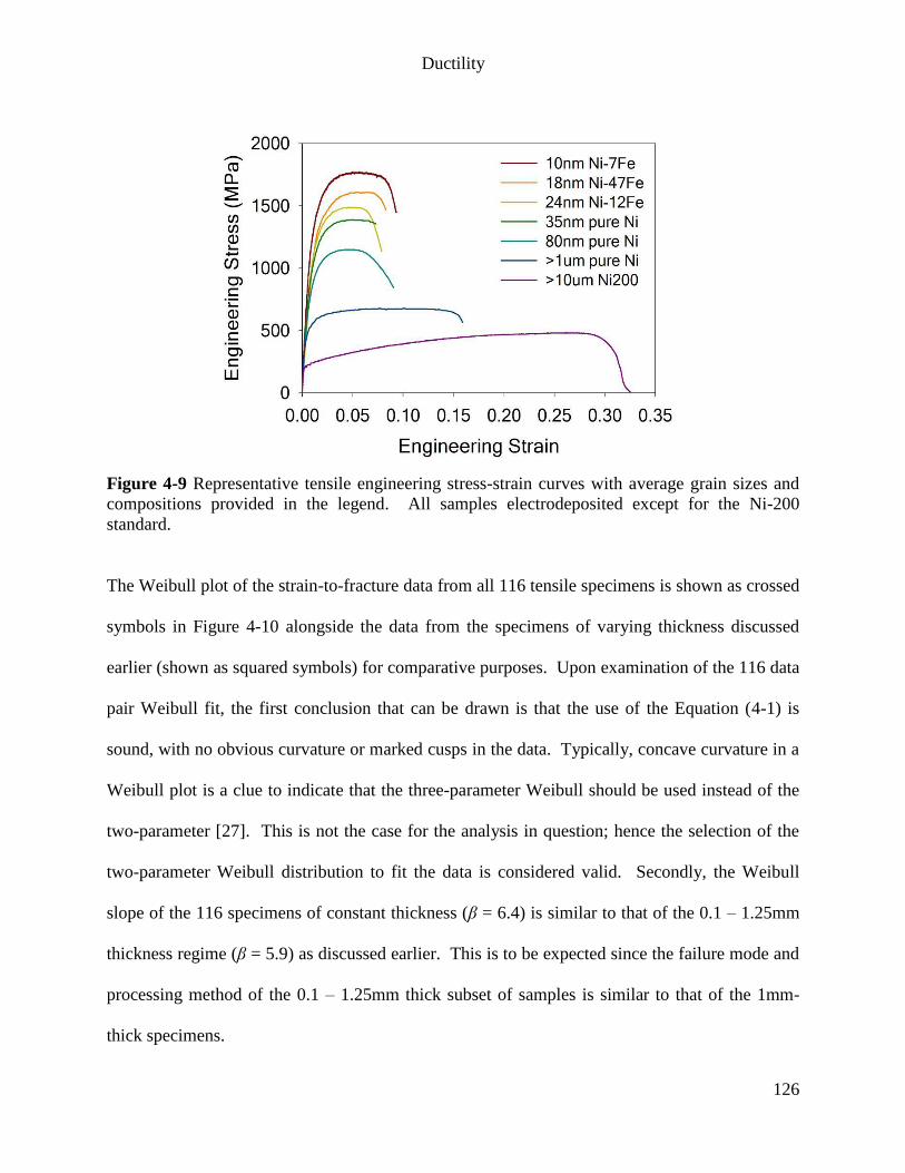
Ductility
126
Figure 4-9 Representative tensile engineering stress-strain curves with average grain sizes and
compositions provided in the legend. All samples electrodeposited except for the Ni-200
standard.
The Weibull plot of the strain-to-fracture data from all 116 tensile specimens is shown as crossed
symbols in Figure 4-10 alongside the data from the specimens of varying thickness discussed
earlier (shown as squared symbols) for comparative purposes. Upon examination of the 116 data
pair Weibull fit, the first conclusion that can be drawn is that the use of the Equation (4-1) is
sound, with no obvious curvature or marked cusps in the data. Typically, concave curvature in a
Weibull plot is a clue to indicate that the three-parameter Weibull should be used instead of the
two-parameter [27]. This is not the case for the analysis in question; hence the selection of the
two-parameter Weibull distribution to fit the data is considered valid. Secondly, the Weibull
slope of the 116 specimens of constant thickness (β = 6.4) is similar to that of the 0.1 – 1.25mm
thickness regime (β = 5.9) as discussed earlier. This is to be expected since the failure mode and
processing method of the 0.1 – 1.25mm thick subset of samples is similar to that of the 1mm-
thick specimens.
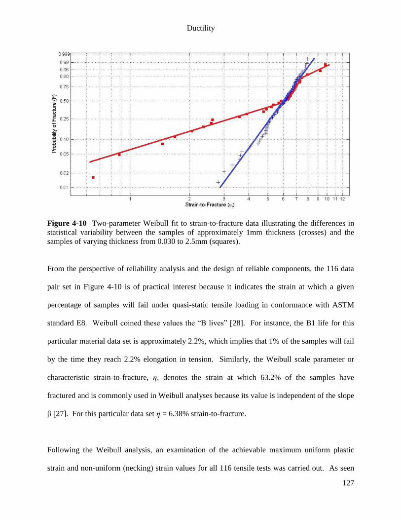
Ductility
127
Figure 4-10 Two-parameter Weibull fit to strain-to-fracture data illustrating the differences in
statistical variability between the samples of approximately 1mm thickness (crosses) and the
samples of varying thickness from 0.030 to 2.5mm (squares).
From the perspective of reliability analysis and the design of reliable components, the 116 data
pair set in Figure 4-10 is of practical interest because it indicates the strain at which a given
percentage of samples will fail under quasi-static tensile loading in conformance with ASTM
standard E8. Weibull coined these values the “B lives” [28]. For instance, the B1 life for this
particular material data set is approximately 2.2%, which implies that 1% of the samples will fail
by the time they reach 2.2% elongation in tension. Similarly, the Weibull scale parameter or
characteristic strain-to-fracture, η, denotes the strain at which 63.2% of the samples have
fractured and is commonly used in Weibull analyses because its value is independent of the slope
β [27]. For this particular data set η = 6.38% strain-to-fracture.
Following the Weibull analysis, an examination of the achievable maximum uniform plastic
strain and non-uniform (necking) strain values for all 116 tensile tests was carried out. As seen
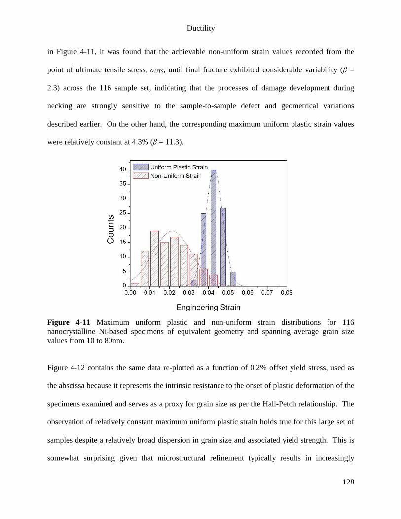
Ductility
128
in Figure 4-11, it was found that the achievable non-uniform strain values recorded from the
point of ultimate tensile stress, σUTS, until final fracture exhibited considerable variability (β =
2.3) across the 116 sample set, indicating that the processes of damage development during
necking are strongly sensitive to the sample-to-sample defect and geometrical variations
described earlier. On the other hand, the corresponding maximum uniform plastic strain values
were relatively constant at 4.3% (β = 11.3).
Figure 4-11 Maximum uniform plastic and non-uniform strain distributions for 116
nanocrystalline Ni-based specimens of equivalent geometry and spanning average grain size
values from 10 to 80nm.
Figure 4-12 contains the same data re-plotted as a function of 0.2% offset yield stress, used as
the abscissa because it represents the intrinsic resistance to the onset of plastic deformation of the
specimens examined and serves as a proxy for grain size as per the Hall-Petch relationship. The
observation of relatively constant maximum uniform plastic strain holds true for this large set of
samples despite a relatively broad dispersion in grain size and associated yield strength. This is
somewhat surprising given that microstructural refinement typically results in increasingly
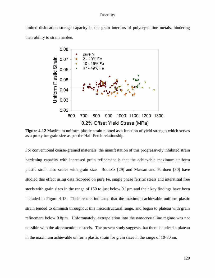
Ductility
129
limited dislocation storage capacity in the grain interiors of polycrystalline metals, hindering
their ability to strain harden.
Figure 4-12 Maximum uniform plastic strain plotted as a function of yield strength which serves
as a proxy for grain size as per the Hall-Petch relationship.
For conventional coarse-grained materials, the manifestation of this progressively inhibited strain
hardening capacity with increased grain refinement is that the achievable maximum uniform
plastic strain also scales with grain size. Bouaziz [29] and Massart and Pardoen [30] have
studied this effect using data recorded on pure Fe, single phase ferritic steels and interstitial free
steels with grain sizes in the range of 150 to just below 0.1µm and their key findings have been
included in Figure 4-13. Their results indicated that the maximum achievable uniform plastic
strain tended to diminish throughout this microstructural range, and began to plateau with grain
refinement below 0.8µm. Unfortunately, extrapolation into the nanocrystalline regime was not
possible with the aforementioned steels. The present study suggests that there is indeed a plateau
in the maximum achievable uniform plastic strain for grain sizes in the range of 10-80nm.
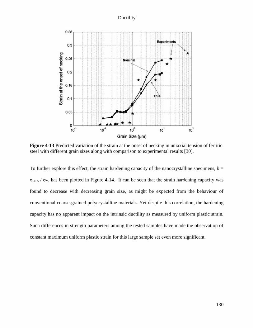
Ductility
130
Figure 4-13 Predicted variation of the strain at the onset of necking in uniaxial tension of ferritic
steel with different grain sizes along with comparison to experimental results [30].
To further explore this effect, the strain hardening capacity of the nanocrystalline specimens, h =
σUTS / σY, has been plotted in Figure 4-14. It can be seen that the strain hardening capacity was
found to decrease with decreasing grain size, as might be expected from the behaviour of
conventional coarse-grained polycrystalline materials. Yet despite this correlation, the hardening
capacity has no apparent impact on the intrinsic ductility as measured by uniform plastic strain.
Such differences in strength parameters among the tested samples have made the observation of
constant maximum uniform plastic strain for this large sample set even more significant.
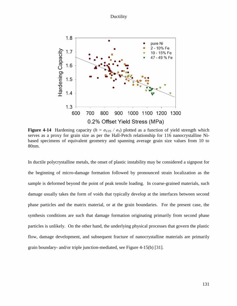
Ductility
131
Figure 4-14 Hardening capacity (h = σUTS / σY) plotted as a function of yield strength which
serves as a proxy for grain size as per the Hall-Petch relationship for 116 nanocrystalline Ni-
based specimens of equivalent geometry and spanning average grain size values from 10 to
80nm.
In ductile polycrystalline metals, the onset of plastic instability may be considered a signpost for
the beginning of micro-damage formation followed by pronounced strain localization as the
sample is deformed beyond the point of peak tensile loading. In coarse-grained materials, such
damage usually takes the form of voids that typically develop at the interfaces between second
phase particles and the matrix material, or at the grain boundaries. For the present case, the
synthesis conditions are such that damage formation originating primarily from second phase
particles is unlikely. On the other hand, the underlying physical processes that govern the plastic
flow, damage development, and subsequent fracture of nanocrystalline materials are primarily
grain boundary- and/or triple junction-mediated, see Figure 4-15(b) [31].
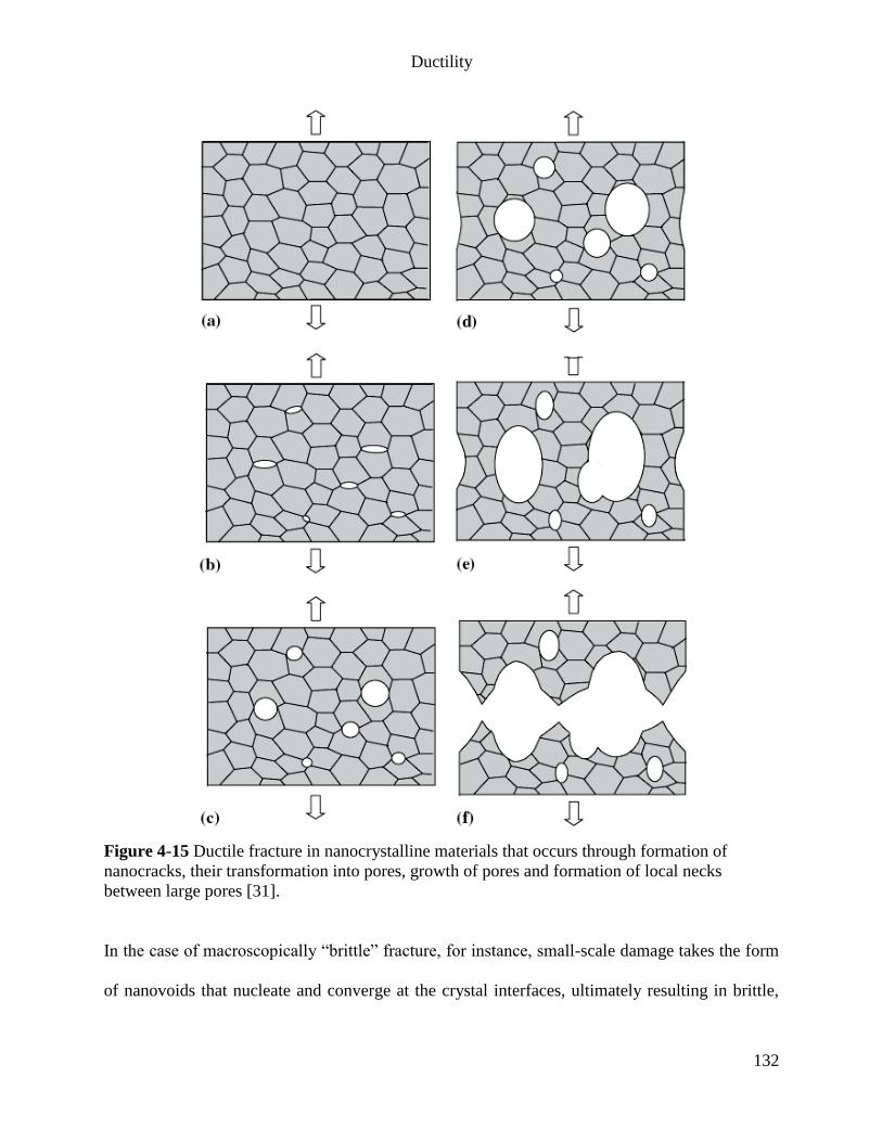
Ductility
132
Figure 4-15 Ductile fracture in nanocrystalline materials that occurs through formation of
nanocracks, their transformation into pores, growth of pores and formation of local necks
between large pores [31].
In the case of macroscopically “brittle” fracture, for instance, small-scale damage takes the form
of nanovoids that nucleate and converge at the crystal interfaces, ultimately resulting in brittle,
Ductility
133
intergranular fracture. On the other hand, if plastic flow and diffusion are intense in the
proximity of the interfaces, the as-formed flat interfacial nanovoids gradually transform into
pores, and with continued external loading, these pores progressively coalesce to form the
dimples that we ultimately observe on the fracture surfaces of macroscopically “ductile”
specimens, e.g. Figure 4-8. In other words, regardless of whether the macroscopic failure mode
is “ductile” or “brittle”, the first stage of nanocrystalline material damage formation remains the
same: localized interfacial decohesion leading to the formation of nanovoids situated at the grain
boundaries and/or triple junctions [31]. While the specific physical mechanisms that contribute
to deformation-induced damage nucleation and growth in ductile nanocrystalline materials are
currently a matter of intense debate [32-34], the present results indicate that, within the grain size
range of 10 to 80nm, this interfacial damage formation seemingly does not strongly depend on
grain size nor bulk material strength (as governed by grain size) but is instead a strain-controlled
phenomenon that can and would be better defined by a critical plastic strain, namely the
maximum uniform plastic strain level.
4.4 Summary and Conclusions
1) The impact of electroforming process control on both the absolute value and variability of
achievable tensile elongation is strong. High variability in tensile strain-to-failure was seen in
samples cut from plates where more defects originating from the process were thought to have
formed in the electrodeposit. On the other hand, samples originating from a more strictly
controlled electroforming process were not only more ductile overall, but were more consistent
from a sample-to-sample tensile strain-to-failure perspective.
Ductility
134
2) The effect of specimen thickness on achievable tensile elongation was studied via
fractography and Weibull distributional analysis of plastic strain-to-failure data of tensile
specimens taken from a set of pure nanocrystalline Ni plates of varying thickness between 0.025
and 2.5mm. As compared to the 0.8-1.25mm thickness range, one can expect much less
predictability in the tensile ductility of either extremely thin monolithic plates of electrodeposited
nanocrystalline Ni where the samples are highly sensitive to the presence of surface flaws or in
extremely thick (greater than approximately 2mm) samples where the presence of critical
ductility controlling volume flaws during lengthy electroforming runs becomes significantly
more problematic.
3) The observed dependency of nanocrystalline Ni tensile ductility on sample thickness was
compared to that of a previous study [21] performed using common engineering metallic
materials encompassing a broad range of mechanical properties. All samples of large cross-
sectional gauge area followed Unwin’s Equation (1-10). However, it was found that, regardless
of the material studied, Unwin’s equation has a tendency to break down for smaller samples
exhibiting a A½/L value below approximately 0.04 mm/mm wherein neck development becomes
increasingly geometry/surface-flaw sensitive with decreasing thickness. Hence, it is concluded
that artifact-reduced electrodeposited nanocrystalline materials behave in a manner similar to
other conventional engineering materials with respect to the dependence of tensile ductility on
specimen shape.
4) Tensile necking elongation in electrodeposited nanocrystalline materials obeys similar
processing quality and geometrical dependencies as in conventional engineering metals.
Ductility
135
5) Unlike conventional engineering metals, intrinsic ductility (as measured by maximum uniform
plastic strain) is unexpectedly independent of microstructure over the grain size range 10-80nm.
This indicates that the underlying physical processes of grain boundary-mediated damage
development are strain-oriented phenomena that can be best defined by a critical plastic strain
regardless of the strength of the material as a whole.
6) The “paradox” between extremely low values of macroscopic elongation-to-fracture in tension
and microscopic ductile fracture surfaces in nanocrystalline materials [35] is mainly a mechanics
(geometry) effect.
7) The prediction of ductility and/or toughness properties using thin samples can be risky and it
is better to carry out mechanical testing on the scale and in the loading mode intended for
component application than to extrapolate based upon material availability. This sensitivity of
tensile elongation to specimen geometry is one of the factors that led Dieter to conclude that, “At
our present degree of understanding, ductility is a qualitative, subjective property of a material”
[10].
4.5 References
[1] N. Wang, Z. Wang, K.T. Aust, U. Erb, Acta Metall. Mater. 43, 2 (1995) 519.
[2] F. Dalla Torre, H. Van Swygenhoven, M. Victoria, Acta Mater. 50 (2002) 3957.
[3] N. Hansen, Adv. Eng. Mater. 7, 9 (2005) 815.
[4] J.R. Weertman, in Nanostructured Materials, second ed., (C.C. Koch (ed.)), William Andrew,
Norwich, NY (2007) 397.
Ductility
136
[5] A.M. El-Sherik, U. Erb, G. Palumbo, K.T. Aust, Scripta Metall. Mater. 27 (1992) 1185.
[6] U. Erb, G. Palumbo, R. Zugic, K.T. Aust, in Processing and Properties of Nanocrystalline
Materials (Eds: C. Suryanarayana et al.), TMS, Warrendale, PA (1996) 93.
[7] C.C. Koch, J. Metastable Nano. Mater. 18 (2003) 9.
[8] C.C. Koch, in Structural Nanocrystalline Materials (C.C. Koch et al. (eds.)), Cambridge
University Press, Cambridge, UK (2007) 134.
[9] Y. Zhao, Y. Zhu, E.J. Lavernia, Adv. Eng. Mater. 12, 8 (2010) 769.
[10] G.E. Dieter, in Metals Handbook, Desk ed, ASM International, Metals Park, OH (1985) 34-
12.
[11] ASTM Standard E8M-01, ASTM International, West Conshohocken, PA (2001).
[12] T. Delahay, T. Palin-Luc, Int. J Fatigue 28 (2006) 474.
[13] W. Weibull, Ingen. Vetenskaps Acad., Proc. 151 (1939) 153.
[14] ASTM Standard C1239-07, ASTM International, West Conshohocken, PA (2007).
[15] X. Teng, H. Mae, Y. Bai, T. Wierzbicki, Eng. Fract. Mech. 75 (2008) 4610.
[16] X. Teng, H. Mae, Y. Bai, T. Wierzbicki, Eng. Fract. Mech. 76 (2009) 983.
[17] H. Hashemi, R. Raiszadeh, J. Appl. Sci. 9, 11 (2009) 2115.
[18] H. Zahedi, M. Emamy, A. Razaghian, M. Mahta, J. Campbell, M. Tiryakioglu, Metall. Mat.
Trans. A38 (2007) 659.
[19] C.C. Koch, K.M. Youssef, R.O. Scattergood, K.L. Murty, Adv. Eng. Mater. 7,9 (2005)797.
[20] A. Misra, X. Zhang, D. Hammon, R.G. Hoagland, Acta Mater. 53 (2005) 221.
[21] E. B. Kula, N.H. Fahey, Mat. Res. Stds (1961) 631.
[22] A. Nadai, Theory of Flow and Fracture of Solids, Vol.1, McGraw-Hill Book Company Inc.,
New York (1950) 319.
Ductility
137
[23] N.H. Lee, J.H. Chen, P.W. Kao, T.Y. Tseng, J.R. Su, Mater. Sci. Eng. A528 (2011) 1979.
[24] A.R. Ragab, S.E. Bayoumi, Engineering Solid Mechanics, CRC Press, Boca Raton (1999)
738.
[25] A. Hasnaoui, H. Van Swygenhoven, P. M. Derlet, Science 300 (2003) 1550.
[26] C. Cheung, F. Djuanda, U. Erb, G. Palumbo, Nanostr. Mater., 5, 5 (1995) 513.
[27] R.B. Abernathy, The New Weibull Handbook, 4th
ed., Gulf Pub. Co, North Palm Beach, Fl
(1996).
[28] W. Weibull, Appl. Mech. 18 (1951) 293.
[29] O. Bouaziz, Adv. Eng. Mater. 11, 10 (2009) 767.
[30] T.J. Massart, T. Pardoen, Acta Mater. 58 (2010) 5768.
[31] I.A. Ovid’ko, in Structural Nanocrystalline Materials (C.C. Koch et al. (eds.)), Cambridge
University Press, Cambridge, UK (2007) 280.
[32] E.M. Bringa, S. Traiviratana, M.A. Meyers, Acta Mater. 58 (2010) 4458.
[33] V.V. Bulatov, W.G. Wolfer, M. Kumar, Scripta Mater. 63 (2010) 144.
[34] I.A. Ovid’ko, A.G. Sheinerman, N.V. Skiba, Acta Mater. 59 (2011) 678.
[35] Z. Shan, J.A. Knapp, D.M. Follstaedt, E.A. Stach, J.M.K. Wiezorek, S.X. Mao, Phys Rev
Lett 100 (2008) 105502.
138
Chapter 5 Hardness-Strength Relationships
The key findings contained in this chapter were previously presented in the following refereed
article: I. Brooks, P. Lin, G. Palumbo, G.D. Hibbard, U. Erb, “Analysis of hardness–tensile
strength relationships for electroformed nanocrystalline materials”, Materials Science and
Engineering A 491 (2008) 412.
5.1 Introduction
A good understanding of the relationships between the hardness and tensile properties of
materials is of considerable importance for several reasons. First, reliable hardness-strength
correlations allow for rapid overall mechanical property evaluations using fast and inexpensive
hardness testing instead of elaborate tensile testing. Second, in contrast to tensile tests, the
hardness of a material can be measured non-destructively in situ on fully assembled components
and devices, thus allowing for structural integrity tests in service, for example in elevated
temperature applications. Third, during the development of new materials, hardness testing is
often the only choice when materials are available in relatively small quantities, insufficient to
perform extensive tensile testing, for example as per ASTM standards. The latter was clearly the
case during the development over the past two decades of the majority of the many
nanocrystalline metals, alloys and composites made using synthesis methods such as inert gas
condensation, vapour phase deposition, electrodeposition, mechanical attrition or crystallization
of amorphous precursors. Most previous studies presented mainly hardness data. Whenever
tensile properties were measured, they were usually obtained on subsize specimen geometries
not in accordance with ASTM standard tests (e.g. ASTM E8). So far, however, no systematic
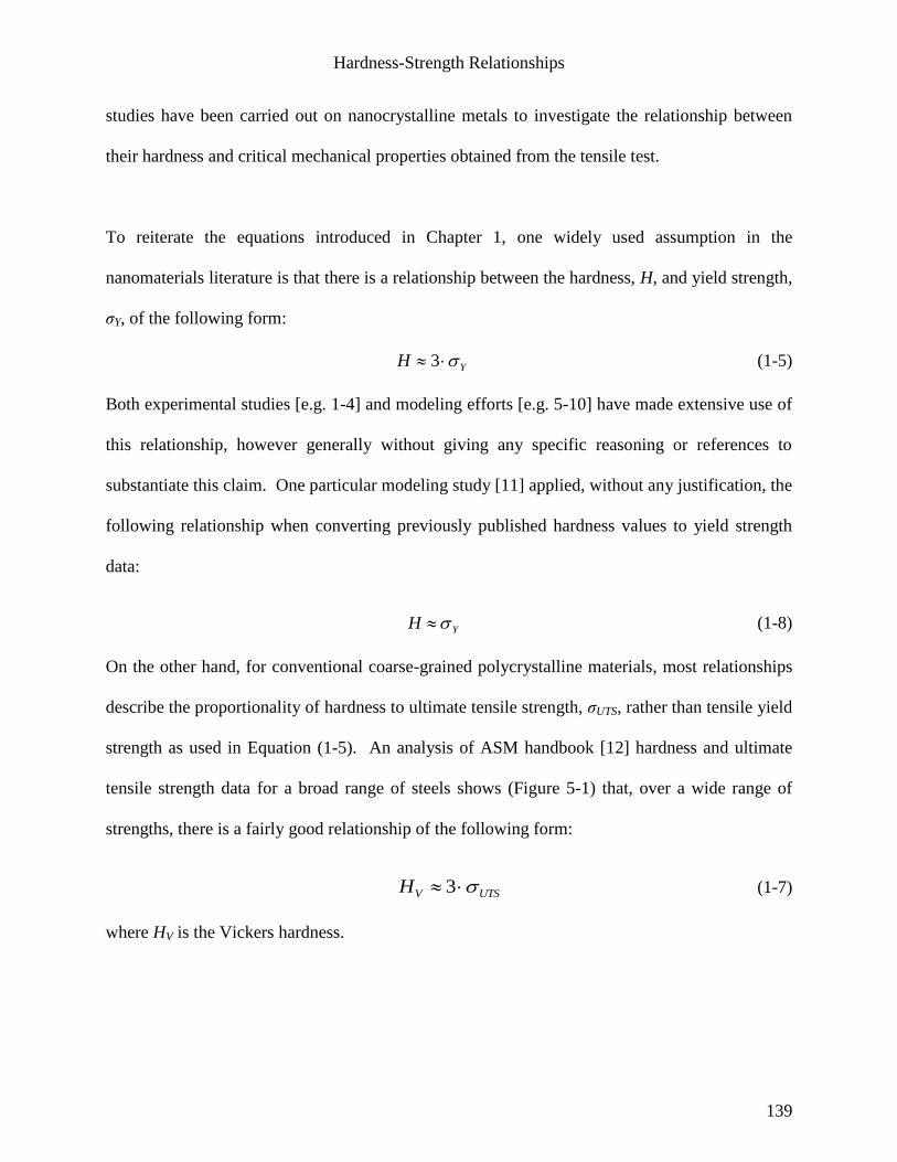
Hardness-Strength Relationships
139
studies have been carried out on nanocrystalline metals to investigate the relationship between
their hardness and critical mechanical properties obtained from the tensile test.
To reiterate the equations introduced in Chapter 1, one widely used assumption in the
nanomaterials literature is that there is a relationship between the hardness, H, and yield strength,
σY, of the following form:
YH 3 (1-5)
Both experimental studies [e.g. 1-4] and modeling efforts [e.g. 5-10] have made extensive use of
this relationship, however generally without giving any specific reasoning or references to
substantiate this claim. One particular modeling study [11] applied, without any justification, the
following relationship when converting previously published hardness values to yield strength
data:
YH (1-8)
On the other hand, for conventional coarse-grained polycrystalline materials, most relationships
describe the proportionality of hardness to ultimate tensile strength, σUTS, rather than tensile yield
strength as used in Equation (1-5). An analysis of ASM handbook [12] hardness and ultimate
tensile strength data for a broad range of steels shows (Figure 5-1) that, over a wide range of
strengths, there is a fairly good relationship of the following form:
UTSVH 3 (1-7)
where HV is the Vickers hardness.
Hardness-Strength Relationships
140
The relationship given in Equation (1-5) has also previously been discussed for coarse-grained
polycrystalline materials [13,14]. However, as pointed out by Ashby and Jones [13] in their
derivation, this relationship is only valid for materials that do not work-harden, i.e. for ideally
plastic materials. In other words, Equation (1-5) should only be used for cases in which the
strength does not change when the hardness indenter is pushed into the surface of the materials.
When a material exhibits work hardening, the proportionality constant, also known as the
“constraint factor”, of 3 is no longer applicable and a correction factor must be applied [13].
Such a scenario has important practical design engineering implications since the continued use
of Equation (1-5) for work hardening materials would effectively result in a potentially
significant over-estimation of the material strength.
Figure 5-1 Vickers hardness as a function of ultimate tensile strength data for carbon and alloy
steels in the annealed, normalized, and quenched-and-tempered conditions [12].
Hardness-Strength Relationships
141
In view of i) the lack of any clear hardness-tensile strength relationships for nanomaterials and ii)
the apparent contradiction between the established relationship (1-7) for coarse-grained
polycrystalline materials and the wide-spread application of Equation (1-5) for nanomaterials,
this study examines the hardness - tensile data relationships for a large number of
electrodeposited nanocrystalline nickel and cobalt-based materials.
5.2 Experimental Details
Data was extracted from all material lots for which Vickers hardness and tensile tests were
carried out on the same test pieces or lots of materials. The data set used for this analysis
comprises a total of 198 individual tensile / hardness tests and includes both materials
synthesized as part of the current study along with data collected from previous members of the
same research group. With respect to experimental details the following should be noted:
i) All materials were synthesized using the electrodeposition method [15,16]. For pure metals,
the plating bath contained only one metallic species (e.g. Ni, Co), while alloys were deposited
from solutions containing two or more ionic species (e.g. Ni-Mo, Ni-Fe, Co-P). Nanocrystalline
Ni-SiC composites were made from a bath containing sub-microcrystalline SiC particles in the
plating solution [17]. All metals were deposited onto Ti cathodes from which they were
subsequently stripped by mechanical means to yield free-standing sheets of varying thicknesses
(0.1 – 3.4 mm) to be cut into suitable specimens for hardness and tensile testing.
Hardness-Strength Relationships
142
ii) The grain sizes of all materials were determined from X-ray line broadening measurements
using the Scherrer approach [18]. For many of the deposits the grain size was also determined
from dark field transmission (TEM) electron micrographs. The grain sizes in the materials
chosen for the current analysis ranged from 80 nm for some of the pure Ni deposits to 7 nm for
the smallest grain sized Ni-Fe deposits. Most of the grain sizes were in the 10-40 nm grain size
range.
iii) Hardness measurements were performed using the Vickers microhardness technique by
measuring the averages of at least 10 indentations each at several locations on each
electrodeposit. The applied loads were 50-200 g depending on the deposit thickness.
iv) Tensile testing was performed on samples with varying gauge dimensions (Table 5-1), which
depended largely on the overall sizes of the available electrodeposit sheets. Most of the tensile
specimens were based upon ASTM standard E8M-01. However, some of the earlier tests used
considerably smaller samples with 5 mm gauge length. The range of gauge volumes was from
2.5 to 535 mm3. The majority of tensile tests were carried out at a strain rate of 5x10
-4 s
-1
although some measurements were performed at other strain rates. The range of 5x10⁻⁵
to
2.5x10⁻³
s-1
encompasses all the test results analyzed in the present study. All samples were
tested to fracture so that yield strength, σY (0.2% offset), ultimate tensile strength, σUTS, and
elongation to fracture, εf, could be recorded.
Table 5-1 Typical gauge dimensions for tensile tests.
Width [mm] Length [mm] Thickness [mm]
2.5-3.0
6.0-6.5
5
25.0-59.5
0.1-0.3
0.1-3.4
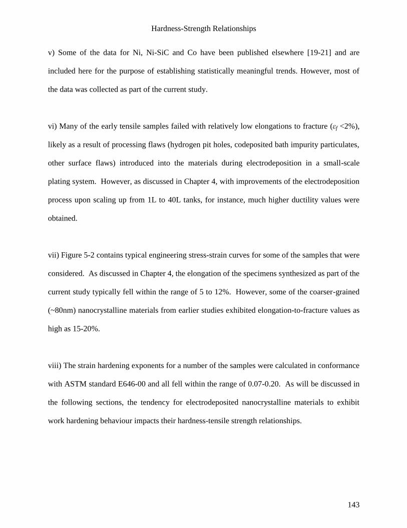
Hardness-Strength Relationships
143
v) Some of the data for Ni, Ni-SiC and Co have been published elsewhere [19-21] and are
included here for the purpose of establishing statistically meaningful trends. However, most of
the data was collected as part of the current study.
vi) Many of the early tensile samples failed with relatively low elongations to fracture (εf <2%),
likely as a result of processing flaws (hydrogen pit holes, codeposited bath impurity particulates,
other surface flaws) introduced into the materials during electrodeposition in a small-scale
plating system. However, as discussed in Chapter 4, with improvements of the electrodeposition
process upon scaling up from 1L to 40L tanks, for instance, much higher ductility values were
obtained.
vii) Figure 5-2 contains typical engineering stress-strain curves for some of the samples that were
considered. As discussed in Chapter 4, the elongation of the specimens synthesized as part of the
current study typically fell within the range of 5 to 12%. However, some of the coarser-grained
(~80nm) nanocrystalline materials from earlier studies exhibited elongation-to-fracture values as
high as 15-20%.
viii) The strain hardening exponents for a number of the samples were calculated in conformance
with ASTM standard E646-00 and all fell within the range of 0.07-0.20. As will be discussed in
the following sections, the tendency for electrodeposited nanocrystalline materials to exhibit
work hardening behaviour impacts their hardness-tensile strength relationships.
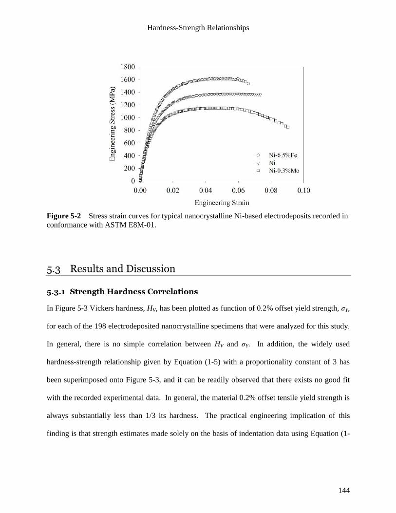
Hardness-Strength Relationships
144
5.3 Results and Discussion
5.3.1 Strength Hardness Correlations
In Figure 5-3 Vickers hardness, HV, has been plotted as function of 0.2% offset yield strength, σY,
for each of the 198 electrodeposited nanocrystalline specimens that were analyzed for this study.
In general, there is no simple correlation between HV and σY. In addition, the widely used
hardness-strength relationship given by Equation (1-5) with a proportionality constant of 3 has
been superimposed onto Figure 5-3, and it can be readily observed that there exists no good fit
with the recorded experimental data. In general, the material 0.2% offset tensile yield strength is
always substantially less than 1/3 its hardness. The practical engineering implication of this
finding is that strength estimates made solely on the basis of indentation data using Equation (1-
Figure 5-2 Stress strain curves for typical nanocrystalline Ni-based electrodeposits recorded in
conformance with ASTM E8M-01.
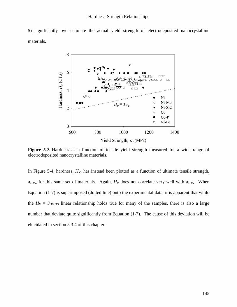
Hardness-Strength Relationships
145
5) significantly over-estimate the actual yield strength of electrodeposited nanocrystalline
materials.
Figure 5-3 Hardness as a function of tensile yield strength measured for a wide range of
electrodeposited nanocrystalline materials.
In Figure 5-4, hardness, HV, has instead been plotted as a function of ultimate tensile strength,
σUTS, for this same set of materials. Again, HV does not correlate very well with σUTS. When
Equation (1-7) is superimposed (dotted line) onto the experimental data, it is apparent that while
the HV = 3·σUTS linear relationship holds true for many of the samples, there is also a large
number that deviate quite significantly from Equation (1-7). The cause of this deviation will be
elucidated in section 5.3.4 of this chapter.
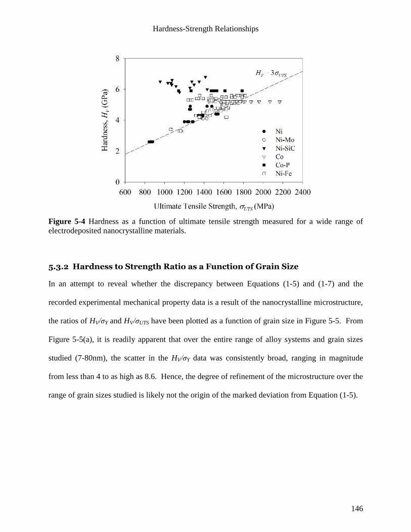
Hardness-Strength Relationships
146
Figure 5-4 Hardness as a function of ultimate tensile strength measured for a wide range of
electrodeposited nanocrystalline materials.
5.3.2 Hardness to Strength Ratio as a Function of Grain Size
In an attempt to reveal whether the discrepancy between Equations (1-5) and (1-7) and the
recorded experimental mechanical property data is a result of the nanocrystalline microstructure,
the ratios of HV/σY and HV/σUTS have been plotted as a function of grain size in Figure 5-5. From
Figure 5-5(a), it is readily apparent that over the entire range of alloy systems and grain sizes
studied (7-80nm), the scatter in the HV/σY data was consistently broad, ranging in magnitude
from less than 4 to as high as 8.6. Hence, the degree of refinement of the microstructure over the
range of grain sizes studied is likely not the origin of the marked deviation from Equation (1-5).
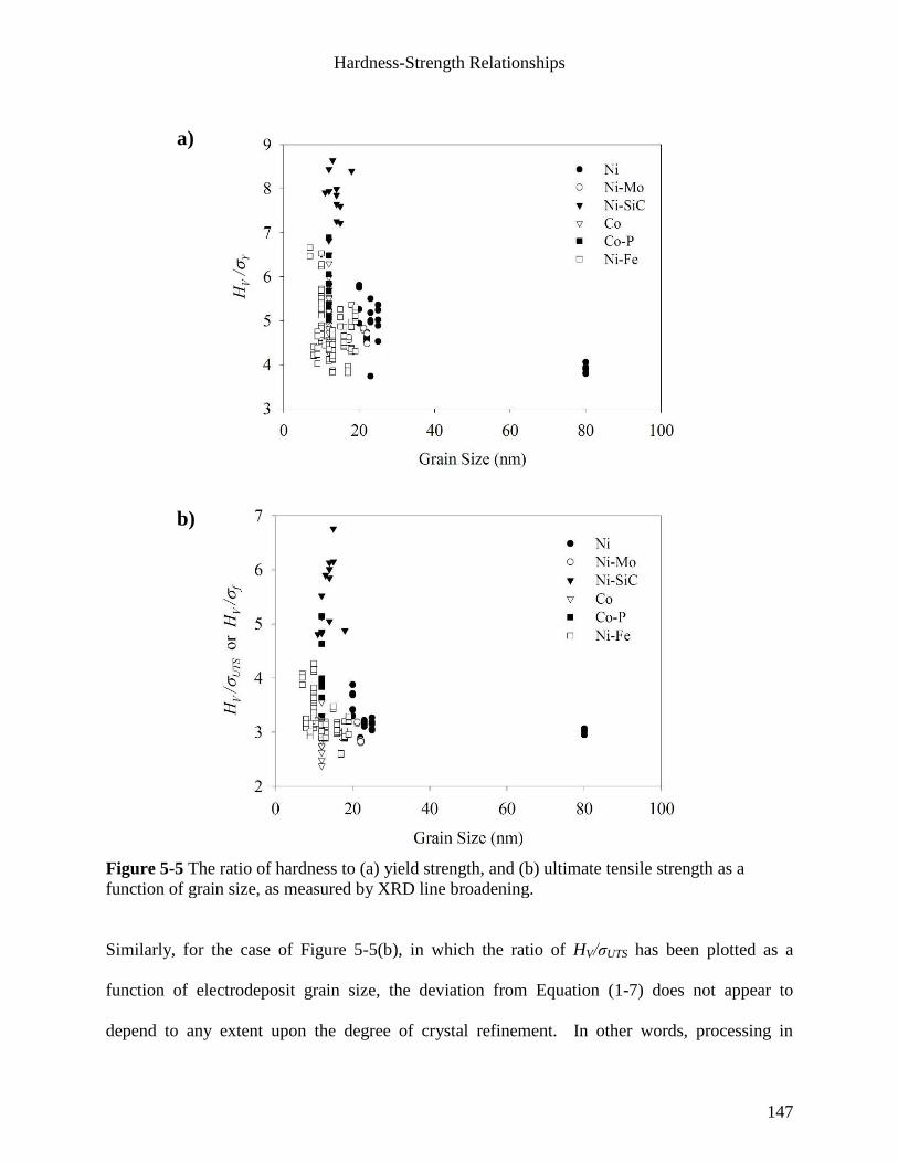
Hardness-Strength Relationships
147
Figure 5-5 The ratio of hardness to (a) yield strength, and (b) ultimate tensile strength as a
function of grain size, as measured by XRD line broadening.
Similarly, for the case of Figure 5-5(b), in which the ratio of HV/σUTS has been plotted as a
function of electrodeposit grain size, the deviation from Equation (1-7) does not appear to
depend to any extent upon the degree of crystal refinement. In other words, processing in
a)
b)
Hardness-Strength Relationships
148
nanocrystalline form, in and of itself, does not appear to be the reason why the mechanical
property data analyzed herein does not correlate well with either Equation (1-5) or (1-7).
5.3.3 Hardness to Strength Ratio as a Function of Gauge Volume
As discussed in Chapter 4, a satisfactory description of the overall intrinsic microstructure-
dependent tensile response of nanomaterials has been hampered by confusion in the literature
surrounding the effect of sample geometry on the shape of the stress-strain curve. Both Dalla
Torre et al. [22] and Fan et al. [23] observed a significant drop in ultimate tensile strength with
increasing sample size, for instance. This behaviour was rationalized as a manifestation of the
“weak link concept” of probabilistic fracture mechanics [24] whereby a larger sample will
exhibit a greater likelihood of possessing a dangerous critical defect within the gauge volume
during tensile testing. Given this context, the impact of tensile gauge volume on the hardness-
strength ratios was examined, and the results are presented in Figure 5-6. In Figure 5-6(a), it is
evident that there exists no clear correlation between HV/σY and tensile gauge volume for this
relatively large sample set that encompasses a very broad range of gauge volumes (2.5 to 535
mm3). Hence, it can be concluded that the breakdown of Equation (1-5) for electrodeposited
nanomaterials cannot be attributed solely to sample size effects.
Similarly, the experimentally recorded HV/σUTS data is presented as a function of tensile test
specimen gauge volume in Figure 5-6(b). In this case, the breadth of the HV/σUTS data does
diminish with increasing gauge volume. However, as mentioned earlier, most of the specimens
corresponding to the smaller gauge volume data points in Figure 5-6 were cut from very thin
foils. As discussed in Chapter 4, thin tensile samples possess a general tendency to fracture early
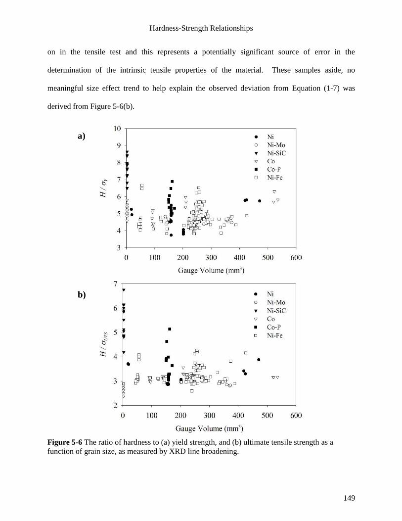
Hardness-Strength Relationships
149
on in the tensile test and this represents a potentially significant source of error in the
determination of the intrinsic tensile properties of the material. These samples aside, no
meaningful size effect trend to help explain the observed deviation from Equation (1-7) was
derived from Figure 5-6(b).
Figure 5-6 The ratio of hardness to (a) yield strength, and (b) ultimate tensile strength as a
function of grain size, as measured by XRD line broadening.
a)
b)
Hardness-Strength Relationships
150
5.3.4 Relationship of Hardness to Ultimate Tensile Strength
In order to reveal how hardness correlates to ultimate tensile strength for the materials examined
in the present study, it is first instructive to summarize the conclusions drawn by Tabor
concerning the proportionality between indentation hardness and ultimate tensile strength for the
Ni, Fe, Cu and Al-based materials employed in his seminal work on the topic [25]:
1) To a first approximation, the ratio of the hardness to the ultimate tensile strength is
independent of the metal under consideration: it depends primarily upon the degree of work
hardening of the metal i.e. on the work hardening exponent n or the Meyer hardness [25]
coefficient m, where m = n + 2;
2) For strain hardening materials, the following expression can be used to describe the hardness-
strength relationship [26]:
)2(
)2(1
)2(5.12)2(1
9.2
m
V
UTSm
mm
H (5-1)
where m = n + 2.
In order to illustrate the magnitude of the strain hardening effect on HV/σUTS, Equation (5-1) has
been plotted in Figure 5-7 and it can be readily observed that the HV/σUTS ratio lies in the range of
2.9 to 3.3 within the domain of n ≤ 0.20 that is applicable to the electrodeposited nanomaterials
considered here. In other words, based upon Tabor’s study of strain hardening metals, one
would expect HV = 3·σUTS to hold reasonably true for the electrodeposited materials analyzed in
the present study owing to the fact that their strain hardening exponents are less than or equal to
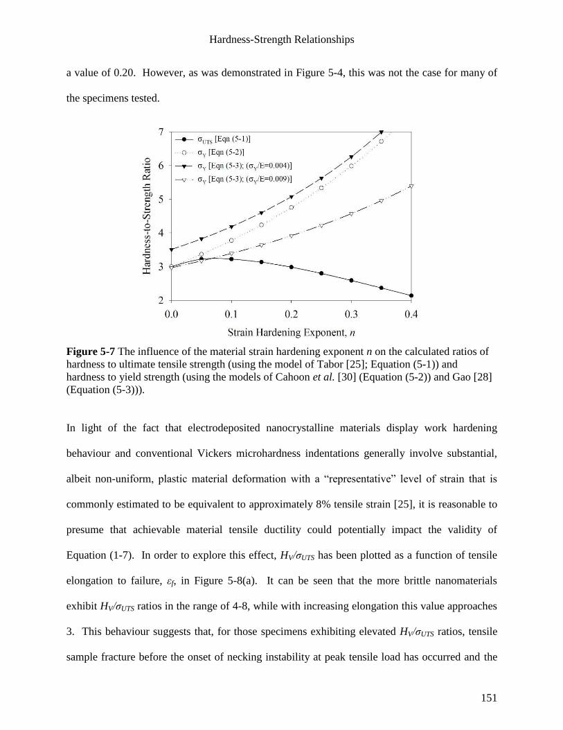
Hardness-Strength Relationships
151
a value of 0.20. However, as was demonstrated in Figure 5-4, this was not the case for many of
the specimens tested.
Figure 5-7 The influence of the material strain hardening exponent n on the calculated ratios of
hardness to ultimate tensile strength (using the model of Tabor [25]; Equation (5-1)) and
hardness to yield strength (using the models of Cahoon et al. [30] (Equation (5-2)) and Gao [28]
(Equation (5-3))).
In light of the fact that electrodeposited nanocrystalline materials display work hardening
behaviour and conventional Vickers microhardness indentations generally involve substantial,
albeit non-uniform, plastic material deformation with a “representative” level of strain that is
commonly estimated to be equivalent to approximately 8% tensile strain [25], it is reasonable to
presume that achievable material tensile ductility could potentially impact the validity of
Equation (1-7). In order to explore this effect, HV/σUTS has been plotted as a function of tensile
elongation to failure, εf, in Figure 5-8(a). It can be seen that the more brittle nanomaterials
exhibit HV/σUTS ratios in the range of 4-8, while with increasing elongation this value approaches
3. This behaviour suggests that, for those specimens exhibiting elevated HV/σUTS ratios, tensile
sample fracture before the onset of necking instability at peak tensile load has occurred and the
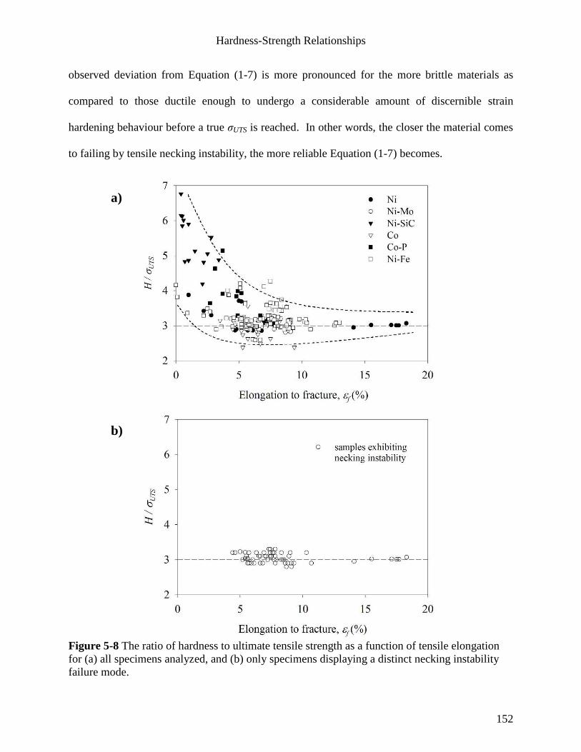
Hardness-Strength Relationships
152
observed deviation from Equation (1-7) is more pronounced for the more brittle materials as
compared to those ductile enough to undergo a considerable amount of discernible strain
hardening behaviour before a true σUTS is reached. In other words, the closer the material comes
to failing by tensile necking instability, the more reliable Equation (1-7) becomes.
Figure 5-8 The ratio of hardness to ultimate tensile strength as a function of tensile elongation
for (a) all specimens analyzed, and (b) only specimens displaying a distinct necking instability
failure mode.
a)
b)
Hardness-Strength Relationships
153
In order to substantiate this hypothesis, a careful examination was made of stress-strain curves,
and a subset originating from tensile specimens that clearly demonstrated plastic deformation
beyond the distinct onset of necking instability was selected. The HV/σUTS ratios for these
samples are presented in Figure 5-8(b) and it can be seen that none deviate significantly from
Equation (1-7). In addition, the fact that these samples encompass a broad range of εf from 6%
to greater than 15% reinforces the importance of deformation until necking instability as opposed
to total achievable elongation to failure per se. It can therefore be concluded that the HV = 3·σUTS
(Equation (1-7)) expression is indeed a reliable predictor of the relationship between hardness
and strength for electrodeposited nanocrystalline materials, provided the material is ductile
enough to sustain tensile deformation before reaching σUTS.
5.3.5 Relationship of Hardness to Yield Strength
The relationship between hardness and yield strength was analyzed in a similar fashion in order
to rationalize the marked deviation of Figure 5-3 data from Equation (1-5). Again, it is
instructive to reiterate the conclusions drawn from previous studies on conventional coarse-
grained metals concerning the relationship between indentation hardness and tensile yield
strength that can be briefly summarized as follows:
1) hardness is an increasing function of yield strength, and for ideally plastic materials (n = 0),
hardness is a linear function with a proportionality constant of ~2.8-3.0 [27];
2) for strain hardening materials (n > 0), the indentation process itself induces an increase in the
measured yield or flow stress response [25];
Hardness-Strength Relationships
154
3) in such instances (n > 0), it has been found that work hardening has a stronger influence on the
force required to move the indenter for materials that exhibit a smaller elastic strain capacity
(small yield strength/elastic modulus ratio) than for materials that are more resistant to the onset
of plastic flow (high σY/E ratio) [28];
4) thus, for so-called “elastic strain-hardening plastic” materials (n > 0), hardness is a multiple
function of σY, n, and E. The implication for the practical application of hardness-yield strength
relationships is that, for a given set of material elastic constants, there are multiple values of σY
and n that can produce the same hardness value [29].
To illustrate the impact of material strain hardening capability on HV/σY, two previously derived
models constructed using completely different strategies were examined. Specifically, the model
of Cahoon et al. [30], which was derived in an empirical fashion and verified experimentally,
was examined alongside the more recent model of Gao [28], which was derived theoretically by
approximating the hardness indentation as a quasi-static expansion of an internally pressurized
spherical shell of an elastic strain-hardening plastic material. In the first case, the proportionality
constant of Equation (1-5) was calculated for a theoretical conventional coarse-grained
polycrystalline metal using the following relationship that was derived by Cahoon et al. [30]:
21.0
3
mV
Y
H (5-2)
where the Meyer hardness coefficient m = n + 2. In their derivation, the authors built upon the
empirical framework of Tabor [25] and then fitted their expression with reasonable accuracy to
experimental data for a number of alloy systems [30]. It is readily apparent from Figure 5-7, in
which this simple empirical expression has been depicted schematically, that the material strain-
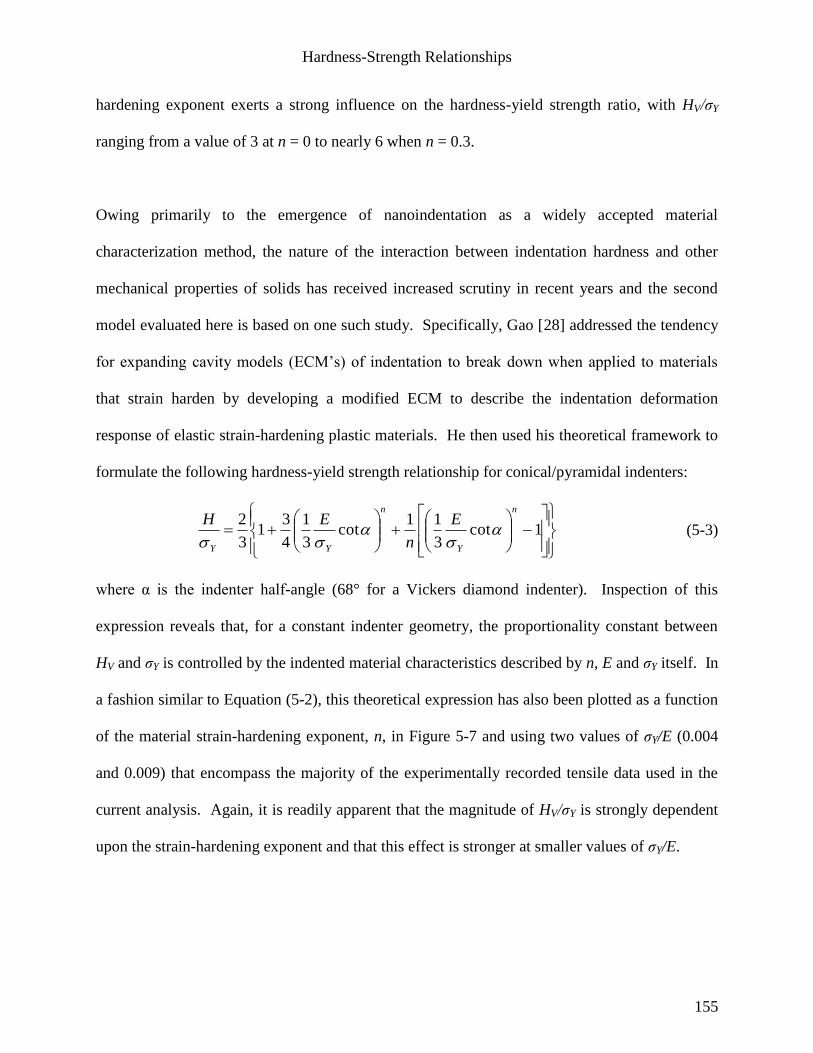
Hardness-Strength Relationships
155
hardening exponent exerts a strong influence on the hardness-yield strength ratio, with HV/σY
ranging from a value of 3 at n = 0 to nearly 6 when n = 0.3.
Owing primarily to the emergence of nanoindentation as a widely accepted material
characterization method, the nature of the interaction between indentation hardness and other
mechanical properties of solids has received increased scrutiny in recent years and the second
model evaluated here is based on one such study. Specifically, Gao [28] addressed the tendency
for expanding cavity models (ECM’s) of indentation to break down when applied to materials
that strain harden by developing a modified ECM to describe the indentation deformation
response of elastic strain-hardening plastic materials. He then used his theoretical framework to
formulate the following hardness-yield strength relationship for conical/pyramidal indenters:
1cot
3
11cot
3
1
4
31
3
2n
Y
n
YY
E
n
EH
(5-3)
where α is the indenter half-angle (68° for a Vickers diamond indenter). Inspection of this
expression reveals that, for a constant indenter geometry, the proportionality constant between
HV and σY is controlled by the indented material characteristics described by n, E and σY itself. In
a fashion similar to Equation (5-2), this theoretical expression has also been plotted as a function
of the material strain-hardening exponent, n, in Figure 5-7 and using two values of σY/E (0.004
and 0.009) that encompass the majority of the experimentally recorded tensile data used in the
current analysis. Again, it is readily apparent that the magnitude of HV/σY is strongly dependent
upon the strain-hardening exponent and that this effect is stronger at smaller values of σY/E.
Hardness-Strength Relationships
156
Equations (5-2) and (5-3) were then used to generate material yield strength estimates on the
basis of experimentally recorded values of HV, n, and E for the same samples shown in Figure 5-
8(b), i.e. the subset of samples that clearly showed necking instability, and the results are
compared to those recorded from tensile testing in Figure 5-9. Upon comparison of the strength
values estimated using the two models to those derived using Equation (1-5), it can be concluded
that accounting for the influence of strain hardening on the hardness-yield strength relationship is
critical if values that approximate those derived from tensile testing are to be expected. It is also
evident from Figure 5-9 that the models of both Cahoon et al. and Gao can be used to
approximate the yield strength of electrodeposited nanomaterials with reasonable accuracy for
some of the samples, while stronger deviation from experimental data exists for others. It is
probable that the origin of any deviation of the calculated σY values from those recorded in
tensile testing is linked to nanomaterial deviation from simple power law hardening behaviour.
Both models use power law hardening as a basic starting assumption, i.e. that the magnitude of n
accurately depicts the strain hardening characteristics of the specimen in question. In other
words, as illustrated in Figure 5-7, both models are quite sensitive to the magnitude of n and their
ability to accurately predict material yield strength on the basis of indentation data is therefore
strongly dependent upon the level of congruence in the magnitude of the strain hardening
exponent n and the actual strain hardening behaviour of the material.
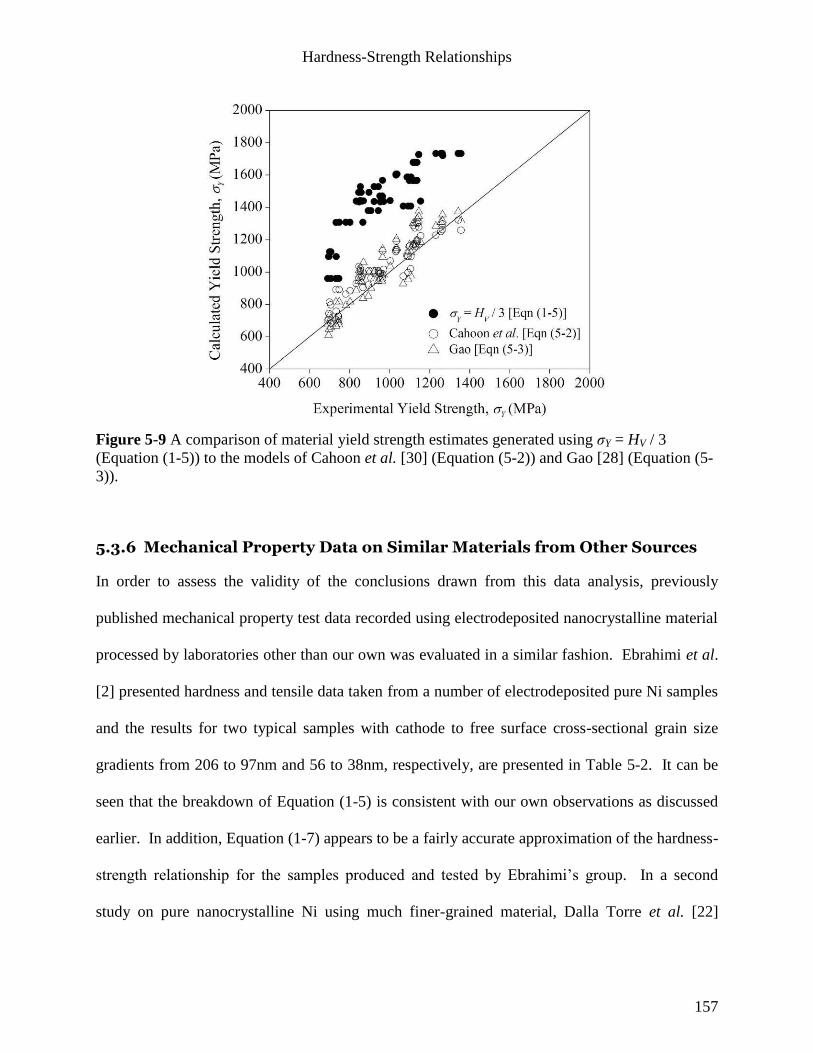
Hardness-Strength Relationships
157
Figure 5-9 A comparison of material yield strength estimates generated using σY = HV / 3
(Equation (1-5)) to the models of Cahoon et al. [30] (Equation (5-2)) and Gao [28] (Equation (5-
3)).
5.3.6 Mechanical Property Data on Similar Materials from Other Sources
In order to assess the validity of the conclusions drawn from this data analysis, previously
published mechanical property test data recorded using electrodeposited nanocrystalline material
processed by laboratories other than our own was evaluated in a similar fashion. Ebrahimi et al.
[2] presented hardness and tensile data taken from a number of electrodeposited pure Ni samples
and the results for two typical samples with cathode to free surface cross-sectional grain size
gradients from 206 to 97nm and 56 to 38nm, respectively, are presented in Table 5-2. It can be
seen that the breakdown of Equation (1-5) is consistent with our own observations as discussed
earlier. In addition, Equation (1-7) appears to be a fairly accurate approximation of the hardness-
strength relationship for the samples produced and tested by Ebrahimi’s group. In a second
study on pure nanocrystalline Ni using much finer-grained material, Dalla Torre et al. [22]
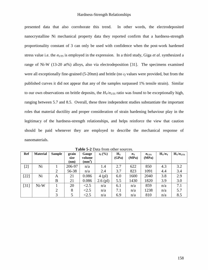
Hardness-Strength Relationships
158
presented data that also corroborate this trend. In other words, the electrodeposited
nanocrystalline Ni mechanical property data they reported confirm that a hardness-strength
proportionality constant of 3 can only be used with confidence when the post-work hardened
stress value i.e. the σUTS is employed in the expression. In a third study, Giga et al. synthesized a
range of Ni-W (13-20 at%) alloys, also via electrodeposition [31]. The specimens examined
were all exceptionally fine-grained (5-20nm) and brittle (no εf values were provided, but from the
published curves it did not appear that any of the samples surpassed 1% tensile strain). Similar
to our own observations on brittle deposits, the HV/σUTS ratio was found to be exceptionally high,
ranging between 5.7 and 8.5. Overall, these three independent studies substantiate the important
roles that material ductility and proper consideration of strain hardening behaviour play in the
legitimacy of the hardness-strength relationships, and helps reinforce the view that caution
should be paid whenever they are employed to describe the mechanical response of
nanomaterials.
Table 5-2 Data from other sources. Ref Material Sample grain
size
(nm)
Gauge
volume
(mm3)
εf (%) HV
(GPa)
σY
(MPa)
σUTS
(MPa)
HV/σY HV/σUTS
[2] Ni 1 206-97 n/a 1.4 2.7 622 850 4.3 3.2
2 56-38 n/a 2.4 3.7 823 1091 4.4 3.4
[22] Ni A 21 0.086 4 (pl) 6.0 1600 2040 3.8 2.9
B 21 0.086 2.6 (pl) 5.5 1430 1820 3.9 3.0
[31] Ni-W 1 20 <2.5 n/a 6.1 n/a 859 n/a 7.1
2 8 <2.5 n/a 7.1 n/a 1238 n/a 5.7
3 5 <2.5 n/a 6.9 n/a 810 n/a 8.5
Hardness-Strength Relationships
159
5.4 Summary and Conclusions
1) Tensile and hardness data from 198 electrodeposited nanocrystalline Ni- and Co-based
specimens of varying shape, composition, microstructure and quality were analyzed in order to
reveal whether any of the established hardness-strength relationships in frequent use for
conventional coarse-grained materials can be applied to this class of materials and, if so, to
elucidate those circumstances under which they might be applied accurately.
2) The majority of the electrodeposited nanomaterials analyzed followed the HV = 3·σUTS
relationship. However, the most brittle specimens tended to diverge from the expected trend
and, in some cases, did so quite significantly. Specifically, for brittle electrodeposited
nanocrystalline materials, the experimentally measured HV/σUTS ratio ranged from ~4-8 and
approached 3 with increasing tensile elongation. It was concluded that the HV = 3·σUTS
expression is a reliable predictor of the relationship between hardness and strength for
electrodeposited nanocrystalline materials, provided the material is ductile enough to sustain
tensile deformation until the onset of necking instability.
3) As it pertains to the nanomaterial HV/σY ratio, the capacity of the material to exhibit strain
hardening behaviour (as described in the present analysis by the magnitude of the strain
hardening exponent n) appears to dictate the magnitude of the proportionality constant between
hardness and yield strength. This is consistent with experimental observations and previously
developed empirical and theoretical modeling of conventional coarse-grained metal systems.
The widely used relationship HV = 3·σY was found to be inapplicable to this class of materials
owing to the fact that they do not deform in an “ideally plastic” manner and instead exhibit
Hardness-Strength Relationships
160
plastic deformation that is characteristic of strain hardening behaviour. This finding has
important practical implications since the application of this commonly used expression results
in potentially significant over-estimations of the intrinsic yield strength of electrodeposited
nanocrystalline materials.
5.5 References
[1] P.G. Sanders, C.J. Youngdahl, J.R. Weertman, Mat. Sci. Eng. A 234 (1997) 77.
[2] F. Ebrahimi, D.G. Bourne, M.S. Kelly, T.E. Matthews, Nanostr. Mat. 11 (1999) 343.
[3] H. Li, F. Ebrahimi, Mat. Sci. Eng. A 347 (2003) 93.
[4] L. Lu, R. Schwaiger, Z.W. Shan, M. Dao, K. Lu, S. Suresh, Acta Mater. 53 (2005) 2169.
[5] J. Lian, B. Baudelet, Nanostr. Mat. 2 (1993) 415.
[6] R.A. Masumura, P.M. Hazzledine, C.S. Pande, Acta Mater. 46 (1998) 4527.
[7] H. Conrad, J. Narayan, Scripta Mater. 42 (2000) 1025.
[8] H. Conrad, J. Narayan, Acta Mater. 50 (2002) 5067.
[9] G.J. Fan, H. Choo, P.K. Liaw, E.J. Lavernia, Mat. Sci. Eng. A 409 (2005) 243.
[10] C.E. Carlton, P.J. Ferreira, Acta Mater. 55 (2007) 3749.
[11] X. Quing, G. Xingmeng, Int. J. Sol. Struct. 43 (2006) 7793.
[12] Metals Handbook, Desk ed, ASM International, Metals Park, OH (1985) 1-60.
[13] M.F. Ashby, D.R.H. Jones, Engineering Materials, Pergamon, Oxford, UK (1980) 81.
[14] M.F. Ashby, H. Shercliff, D. Cebon D, Materials Engineering, Science, Processing and
Design, Elsevier, Oxford, UK (2007) 115.
[15] U. Erb, A.M. El-Sherik, US Patent #5,352,266 (1994).
[16] U. Erb, A.M. El-Sherik, C.K.S. Cheung, M.J. Aus, US Patent #5,433,797 (1995).
Hardness-Strength Relationships
161
[17] A.F. Zimmerman, D.G. Clark, K.T. Aust, U. Erb, Mat. Lett. 52 (2002) 85.
[18] B.D. Cullity, Elements of X-ray Diffraction, second ed., Addison-Wesley, Reading, MA
(1978) 102.
[19] A.F. Zimmerman, G. Palumbo, K.T. Aust, U. Erb, Mater. Sci. Eng. A 328 (2002) 137.
[20] A.A. Karimpoor, U. Erb, K.T. Aust, Z. Wang, G. Palumbo, J. Metast. Nanostr. Mater. 13
(2002) 415.
[21] A.A. Karimpoor, U. Erb, K.T. Aust, G. Palumbo, Scripta Mater. 49 (2003) 252.
[22] F. Dalla Torre, H. Van Swygenhoven, M. Victoria, Acta Mater. 50 (2002) 3957.
[23] G.J. Fan, L.F. Fu, H. Choo, P.W. Liaw, N.D. Browning, Acta Mater. 54 (2006) 4781.
[24] G.E. Dieter, Mechanical Metallurgy, SI Metric ed., McGraw-Hill, London, UK (1988) 370.
[25] D. Tabor, The Hardness of Metals, Clarendon, Oxford, UK (1951) 1.
[26] D. Tabor, J. Inst. Metals 79 (1951) 1.
[27] A. Nayebi, R. El Abdi, O. Bartier, G. Mauvoisin, Mech. Mater. 34 (2002) 243.
[28] X.L. Gao, Int. J. Solids Struct. 43 (2006) 6615.
[29] Y.T. Cheng, C.M. Cheng, Mater. Sci. Eng. R 44 (2004) 91.
[30] J.R. Cahoon, W.H. Broughton, A.R. Kutzak, Metall. Trans. 2 (1971) 1979.
[31] A. Giga, Y. Kimoto, Y. Takigawa, K. Higashi, Scripta Mater. 55 (2006) 143.
162
Chapter 6 Conclusions
Conclusion #1
A great deal of work has been devoted to the study of nanocrystalline materials and their
mechanical properties. However, some of the most important mechanical properties, such as
achievable ductility and elastic modulus, are known to be highly sensitive to the presence of
processing artifacts. This study demonstrated that electroformed specimens substantially
reduced in defects such as hydrogen pitting, chemical contamination, and particulate
contamination could be reproducibly synthesized through adoption of specific strategies such as
steady state chemical control, fine particulate filtering, and improved feedstock chemical quality.
Conclusion #2
An inability in past studies to produce bulk quantities of nanocrystalline materials has prevented
tensile testing according to standardized test protocols such as ASTM E8. Consequently, the
persistent use of non-standardized miniature specimen geometries has resulted in considerable
confusion concerning the intrinsic mechanical properties of nanocrystalline materials. It was
found that processing artifact reduction and electrodeposit internal stress control in large 40L
electroforming tanks enabled the systematic production of artifact-reduced 152mm x 152 mm
plates of 1mm thickness and beyond. As a result, nanocrystalline materials could be tensile
tested in conformance with ASTM E8. This had not been possible prior to this study.
Conclusions
163
Conclusion #3
Because the linear extension that may be sustained by a typical mechanical test specimen loaded
in tension is not a deterministic material-specific property but instead reflects a distribution (size
and orientation) of flaws present in the material in addition to the intrinsic material ductility and
specimen size and shape dependencies, a thorough analysis of nanocrystalline material ductility
required a statistically significant set of specimens. To this end, 161 specimens were tensile
tested as part of this study. This large number of samples enabled a statistical evaluation of
achievable ductility by Weibull distributional analysis.
Conclusion #4
The primary material “quality” criterion used throughout this work was achievable tensile
elongation-to-fracture of multiple samples cut from each individual plate produced. It was found
that the impact of electroforming process control on both the absolute value and variability of
achievable tensile elongation was strong. In particular, high variability in tensile strain-to-failure
was seen in samples cut from plates where more defects originating from the process were
thought to have formed in the electrodeposit. On the other hand, samples originating from a
more strictly controlled electroforming process were not only more ductile overall, but were
more consistent from a sample-to-sample tensile strain-to-failure perspective.
Conclusion #5
The effect of specimen thickness on achievable tensile elongation was studied via fractography
and Weibull distributional analysis of plastic strain-to-failure data of tensile specimens taken
from a set of pure nanocrystalline Ni plates of varying thickness between 0.025 and 2.5mm. As
Conclusions
164
compared to the 0.8-1.25mm thickness range, much less predictability was observed in the
tensile ductility of either extremely thin monolithic plates of electrodeposited nanocrystalline Ni
where the fracture mode was highly sensitive to the presence of surface flaws. Similarly, less
predictability was observed in the tensile ductility of extremely thick (greater than approximately
2mm) samples where the presence of critical ductility controlling volume flaws during lengthy
electroforming runs may have become significantly more problematic.
Conclusion #6
The observed dependency of nanocrystalline Ni tensile ductility on sample thickness was
compared to that of a previous study performed using common engineering metallic materials
encompassing a broad range of mechanical properties. All samples of large cross-sectional
gauge area followed Unwin’s equation. However, it was found that, regardless of the material
studied, Unwin’s equation has a tendency to break down for smaller samples exhibiting a A½/L
value below approximately 0.04 mm/mm as the neck development becomes increasingly
geometry/surface-flaw sensitive with decreasing thickness.
Conclusion #7
Tensile necking elongation in electrodeposited nanocrystalline materials obeys similar
processing quality and geometrical dependencies as in conventional engineering metals.
Conclusion #8
Unlike conventional engineering metals, intrinsic ductility (as measured by maximum uniform
plastic strain) was unexpectedly observed to be independent of microstructure over the grain size
Conclusions
165
range 10-80nm. This indicated that the underlying physical processes of grain boundary-
mediated damage development are strain-oriented phenomena that can be best defined by a
critical plastic strain regardless of the strength of the material as a whole.
Conclusion #9
The “paradox” between extremely low values of macroscopic elongation-to-fracture in tension
and microscopic ductile fracture surfaces in nanocrystalline materials is mainly a mechanics
(geometry) effect.
Conclusion #10
The prediction of ductility and/or toughness properties using thin samples can be risky and it is
better to carry out mechanical testing on the scale and in the loading mode intended for
component application than to extrapolate based upon material availability. This sensitivity of
tensile elongation to specimen geometry is one of the main reasons why ductility remains a
subjective property of a material.
Conclusion #11
Despite the widespread use of hardness testing of nanocrystalline materials as a proxy for
strength testing, there was a persistent lack of clarity as to which hardness-tensile strength
relationships could be reliably applied prior to this study. Data from a large number of 196
samples was evaluated. It was found that the majority of electrodeposited nanomaterials
analyzed followed the HV = 3·σUTS relationship. However, samples that exhibited little tensile
plasticity tended to diverge from the expected trend and, in some cases, did so quite significantly.
Conclusions
166
It was concluded that the HV = 3·σUTS expression is a reliable predictor of the relationship
between hardness and strength for electrodeposited nanocrystalline materials, provided the
material is ductile enough to sustain tensile deformation until the onset of necking instability.
Conclusion #12
As it pertains to the nanomaterial HV/σY ratio, the capacity of the material to exhibit strain
hardening behaviour appears to dictate the magnitude of the proportionality constant between
hardness and yield strength. This is consistent with experimental observations and previously
developed empirical and theoretical modeling of conventional coarse-grained metal systems.
The widely used relationship HV = 3·σY was found to be inapplicable to this class of materials
owing to the fact that they do not deform in an “ideally plastic” manner and instead exhibit
plastic deformation that is characteristic of strain hardening behaviour. This finding has
important practical implications since the application of this commonly used expression results
in potentially significant over-estimations of the intrinsic yield strength of electrodeposited
nanocrystalline materials.
167
Chapter 7 Recommendations for Future Work
Recommendation #1
While significant advancements in the synthesis of bulk quantities of artifact-free nanocrystalline
materials by electrodeposition have been made as part of this study, there is room for further
improvement. In particular, there exists a need for even more processing artifact removal. This
could conceivably be accomplished through a combination of ultrafine (<1µm pore size) filtering
and further solution flow pattern optimization to ensure the complete absence of solid matter in
the catholyte. In addition, the identification of a method to quantify the co-deposited anode
particulate content would greatly assist in the development of a ductility-particulate
concentration relationship for this material class, similar to that presented in Figure 1-16.
Recommendation #2
Another primary objective of this study was to explore the intrinsic ductility of electrodeposited
nanocrystalline materials. While tensile testing in conformance with ASTM E8 is the most
broadly accepted methodology to do so, there are other techniques that should be considered.
Most notably, fracture toughness is another important measure of material ductility.
The plane strain fracture toughness, KIc, of a metallic material refers to the crack-extension
resistance under conditions of crack-tip plane strain in Mode I cracking and involves increasing-
force tests of fatigue precracked specimens. In other words, the test provides information on the
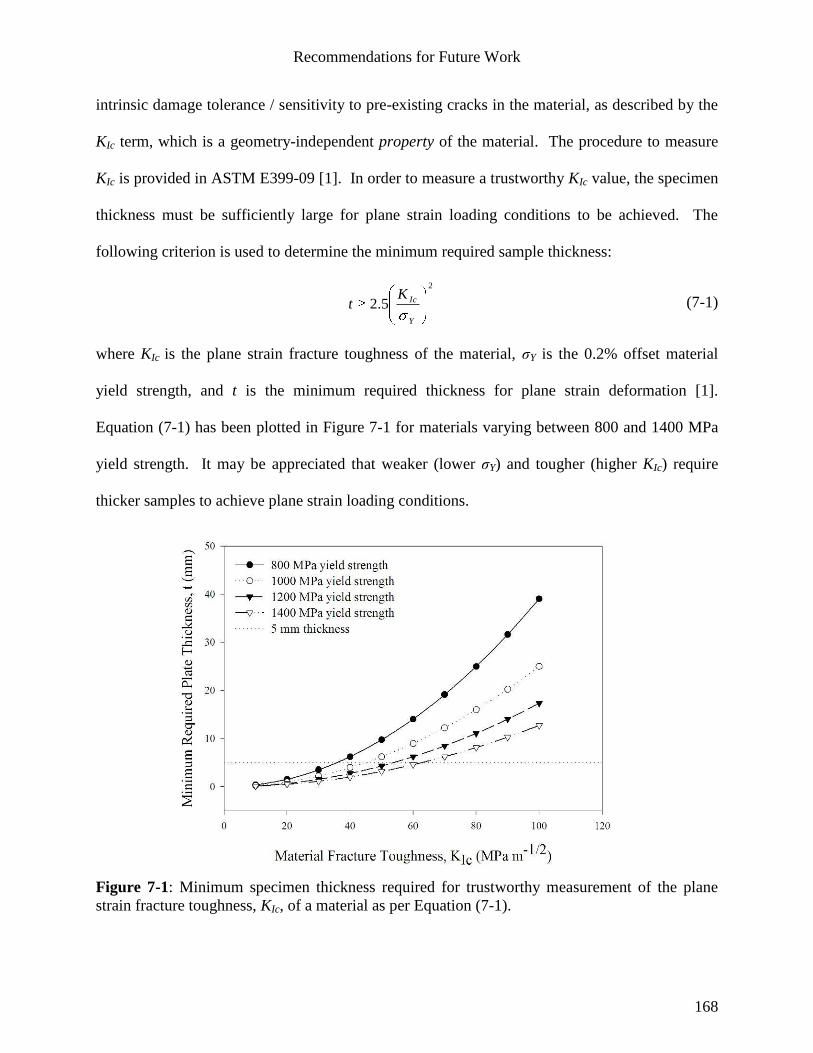
Recommendations for Future Work
168
intrinsic damage tolerance / sensitivity to pre-existing cracks in the material, as described by the
KIc term, which is a geometry-independent property of the material. The procedure to measure
KIc is provided in ASTM E399-09 [1]. In order to measure a trustworthy KIc value, the specimen
thickness must be sufficiently large for plane strain loading conditions to be achieved. The
following criterion is used to determine the minimum required sample thickness:
2
5.2Y
IcKt (7-1)
where KIc is the plane strain fracture toughness of the material, σY is the 0.2% offset material
yield strength, and t is the minimum required thickness for plane strain deformation [1].
Equation (7-1) has been plotted in Figure 7-1 for materials varying between 800 and 1400 MPa
yield strength. It may be appreciated that weaker (lower σY) and tougher (higher KIc) require
thicker samples to achieve plane strain loading conditions.
Figure 7-1: Minimum specimen thickness required for trustworthy measurement of the plane
strain fracture toughness, KIc, of a material as per Equation (7-1).
Recommendations for Future Work
169
There have been relatively few attempts to measure KIc in nanocrystalline materials. One study
by Hanlon et al. on electrodeposited nanocrystalline Ni indicated that the plane stress fracture
toughness value for this material was 25 MPa·m-1/2
[2]. Application of Equation (7-1) with 25
MPa·m-1/2
as the plane strain fracture toughness value and 1000 MPa as the material yield
strength reveals that a minimum specimen thickness of 1.56 mm would be required to achieve
plane strain deformation and thereby measure a trustworthy KIc value for that material.
As an aside to the present study, a very thick (~5 mm) plate of electrodeposited nanocrystalline
Ni-15wt%Fe (~1300 MPa yield strength) was prepared and subjected to testing in conformance
with ASTM E399-09. Part of the ASTM E399-09 standard specification is a protocol for testing
for plane strain deformation and it was found that a condition of plane strain loading was not
achieved for the 5mm-thick Ni-Fe sample. In other words, the 5mm specimen thickness of this
particular material was insufficient to record a trustworthy KIc value. Application of Equation
(7-1) with the aforementioned 5mm thickness and 1300 MPa yield strength values reveals that
the plane strain fracture toughness value of this material was therefore at least 58.1
MPa·m-1/2
. Future work directed towards the measurement of a plane strain fracture toughness
value for an electrodeposited nanocrystalline material would be enabled by the development of a
synthesis method to produce plates in excess of 5mm thickness.
Recommendation #3
The engineering stress-strain data presented in this report indicate the presence of strain
hardening behaviour in electrodeposited nanocrystalline materials. Given the small grain size,
traditional mechanisms of intracrystalline dislocation interaction are unlikely in nanocrystalline
Recommendations for Future Work
170
materials. The underlying mechanistic nature of the observed strain hardening behaviour
requires further study.
References
[1] ASTM Standard E399-09, ASTM International, West Conshohocken, PA (2009).
[2] T. Hanlon, L. Prchlik, S. Suresh, unpublished results, as reported in K.S. Kumar, H. Van
Swygenhoven, S. Suresh, Acta Mater. 51 (2003) 5743.
171
Appendix A Plastic Deformation Mechanisms in Nanocrystalline Materials: An Overview
A.1 Introduction
The nano-scale plastic deformation mechanisms that underpin the Figure 1-6 variation of
strength/hardness as a function of grain size have been quite difficult to observe and measure
directly. Therefore, the field has adopted a three-fold strategy to reveal the underlying
mechanisms, namely:
1. Improved techniques for compiling direct experimental evidence;
2. Computer simulations; and
3. Development of analytical theoretical models
The common goal has been to study nanomaterial plasticity using these fundamentally dissimilar
methods, and then aggregate the individual findings in the interest of answering the central
question behind them all, namely, “How do nanocrystalline materials deform?”
A.2 Experimental Observations
As mentioned in Section 1.3.2, while TEM represents a powerful tool to study deformation
mechanisms in metallic materials, there have been difficulties in extending the technique for
direct observation of nanomaterial plasticity, due most notably to grain overlap [1], practical
difficulties in loading these high strength materials while simultaneously observing dynamic
plasticity in situ in the TEM, and concerns over thin foil surface effects [2]. Most early TEM
Appendix A
172
studies did not observe dislocations and theoretical speculations suggested that they might not
exist because of large image forces that would pull them into the boundaries along with difficulty
in activating traditional dislocation sources such as the Frank-Read source. However,
subsequent work by Milligan et al. [1] and Ke et al. [3] solved the grain overlap problem by
restricting study to thin sputtered films. At grain sizes below 25nm, no dislocations were
observed. Signs of significant plasticity were nevertheless noted and attributed to diffusion
assisted grain boundary deformation processes. Larger grains showed significant dislocation
activity.
In 2001, Youngdahl et al. [4] used the emerging capability of TEM video to record in situ
deformation of inert gas condensed nanocrystalline Cu. They reported dislocation activity down
to 30nm in grain size but encountered grain overlap problems below that size. In 2003, Kumar et
al. [5] carried out video TEM of 30nm grain size electrodeposited nanocrystalline Ni that was
mechanically loaded in situ. Evidence of extensive dislocation activity was observed and it
appeared as though dislocations were emitted from grain boundaries. However, this could not
account for the high levels of plasticity imparted to the specimen. Voids were also observed
along grain boundaries. It was therefore concluded that the observed deformation
accommodation could be attributed to a combination of dislocation-based plasticity and
nucleation and growth of voids.
In 2004, Shan et al. used dark-field video TEM to study the deformation of plasma deposited
nanocrystalline Ni, this time with a smaller average grain size of 10nm [6]. They concluded that
grain boundary diffusion-controlled grain rotation and agglomeration were the predominant
Appendix A
173
mechanisms by which plastic flow was accommodated in their specimens. Similar conclusions
were also drawn by Jin et al. [7] who made direct in situ TEM observations of grain boundary
migration, grain rotation and grain coalescence in ultrafine-grained Al under the influence of
externally applied indentation.
More recently, in 2008, Wang et al. carried out in situ tensile deformation of 20nm grain size
electrodeposited nanocrystalline Ni in the TEM [8] and also observed grain rotation and
neighbouring grain rotation/growth under the influence of tensile loading. A schematic
representation of the deformation mechanism proposed by the authors as a result of their TEM
observations is included in Figure A-1. Based upon their direct observations, it was concluded
that deformation-induced grain boundary sliding leading to grain rotation and, ultimately, grain
coalescence/growth are active plastic deformation mechanisms in electrodeposited
nanocrystalline Ni [8]. Once again, however, such TEM observations of grain rotation are
somewhat controversial because the TEM foils are very thin and may not represent bulk
nanocrystalline materials [2].
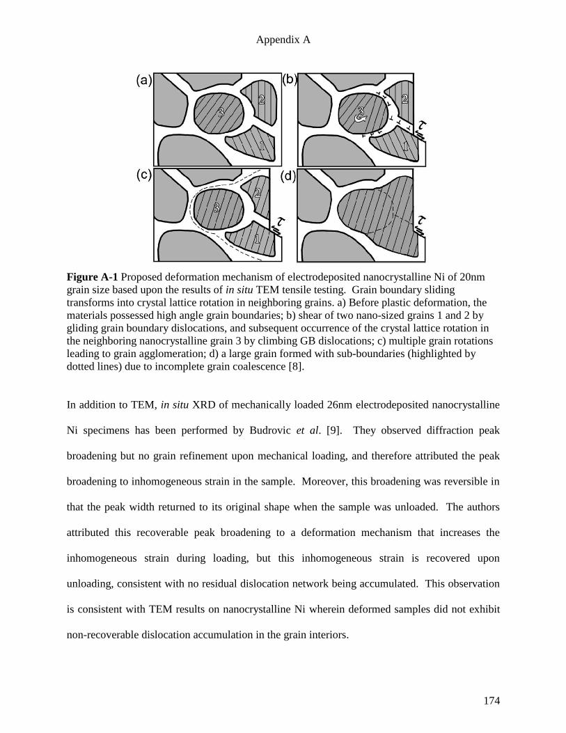
Appendix A
174
Figure A-1 Proposed deformation mechanism of electrodeposited nanocrystalline Ni of 20nm
grain size based upon the results of in situ TEM tensile testing. Grain boundary sliding
transforms into crystal lattice rotation in neighboring grains. a) Before plastic deformation, the
materials possessed high angle grain boundaries; b) shear of two nano-sized grains 1 and 2 by
gliding grain boundary dislocations, and subsequent occurrence of the crystal lattice rotation in
the neighboring nanocrystalline grain 3 by climbing GB dislocations; c) multiple grain rotations
leading to grain agglomeration; d) a large grain formed with sub-boundaries (highlighted by
dotted lines) due to incomplete grain coalescence [8].
In addition to TEM, in situ XRD of mechanically loaded 26nm electrodeposited nanocrystalline
Ni specimens has been performed by Budrovic et al. [9]. They observed diffraction peak
broadening but no grain refinement upon mechanical loading, and therefore attributed the peak
broadening to inhomogeneous strain in the sample. Moreover, this broadening was reversible in
that the peak width returned to its original shape when the sample was unloaded. The authors
attributed this recoverable peak broadening to a deformation mechanism that increases the
inhomogeneous strain during loading, but this inhomogeneous strain is recovered upon
unloading, consistent with no residual dislocation network being accumulated. This observation
is consistent with TEM results on nanocrystalline Ni wherein deformed samples did not exhibit
non-recoverable dislocation accumulation in the grain interiors.
Appendix A
175
Tensile deformation with in situ XRD of electrodeposited nanocrystalline Ni-Fe was also carried
out by Fan et al. in 2006 [10]. XRD microstrain, which the authors asserted is related to the
dislocation density of the materials, did not change after plastic deformation in the uniformly
deforming section of the tensile specimen. This result indicated that the nanocrystalline Ni–Fe
alloy, if deformed uniformly, does not exhibit dislocation accumulation, an observation that
agreed with the results obtained by Budrovic et al. [9]. However, the XRD measurements also
indicated that dislocation motion appears to become more active in the post-uniform or localized
necking regime of tensile deformation, coincident with strong crystallographic texture
development, grain rotation and a slight increase in the microstrain of the sample. In particular,
the observed increase in XRD microstrain was attributed to dislocation accumulation, which the
authors argued was possible due to the formation of larger crystals resulting from deformation-
induced grain coarsening in the necking region as compared with the relatively small grain sizes
in the uniformly deforming region of the specimen. Indeed, post-mortem TEM on the specimens
indicated that the average grain size of the material in the gauge section of the tensile tested
specimen had increased from 23 nm in the as-deposited state to 73 nm in the deformed condition
as a result of stress-induced grain coarsening.
These in situ TEM and XRD observations of nanocrystalline material deformation demonstrate
that grain boundary sliding and grain rotation may play a significant role in the deformation of
nanocrystalline materials, and that sufficiently high levels of plastic deformation can lead to
deformation-induced grain growth. Moreover, these observations of plasticity in nanocrystalline
materials point towards a transition from conventional lattice dislocation slip to deformation
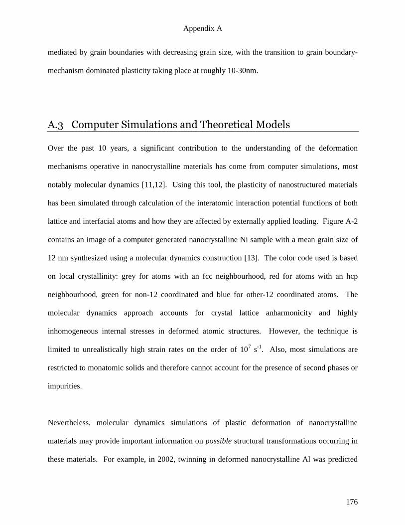
Appendix A
176
mediated by grain boundaries with decreasing grain size, with the transition to grain boundary-
mechanism dominated plasticity taking place at roughly 10-30nm.
A.3 Computer Simulations and Theoretical Models
Over the past 10 years, a significant contribution to the understanding of the deformation
mechanisms operative in nanocrystalline materials has come from computer simulations, most
notably molecular dynamics [11,12]. Using this tool, the plasticity of nanostructured materials
has been simulated through calculation of the interatomic interaction potential functions of both
lattice and interfacial atoms and how they are affected by externally applied loading. Figure A-2
contains an image of a computer generated nanocrystalline Ni sample with a mean grain size of
12 nm synthesized using a molecular dynamics construction [13]. The color code used is based
on local crystallinity: grey for atoms with an fcc neighbourhood, red for atoms with an hcp
neighbourhood, green for non-12 coordinated and blue for other-12 coordinated atoms. The
molecular dynamics approach accounts for crystal lattice anharmonicity and highly
inhomogeneous internal stresses in deformed atomic structures. However, the technique is
limited to unrealistically high strain rates on the order of 107 s
-1. Also, most simulations are
restricted to monatomic solids and therefore cannot account for the presence of second phases or
impurities.
Nevertheless, molecular dynamics simulations of plastic deformation of nanocrystalline
materials may provide important information on possible structural transformations occurring in
these materials. For example, in 2002, twinning in deformed nanocrystalline Al was predicted
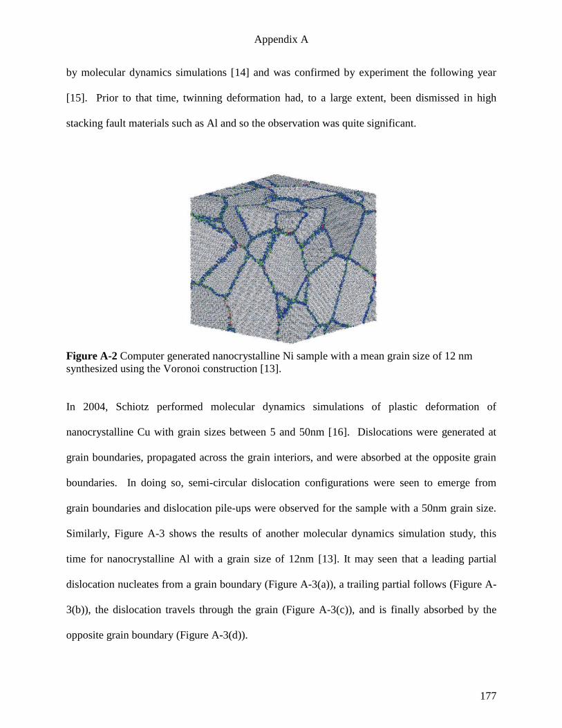
Appendix A
177
by molecular dynamics simulations [14] and was confirmed by experiment the following year
[15]. Prior to that time, twinning deformation had, to a large extent, been dismissed in high
stacking fault materials such as Al and so the observation was quite significant.
Figure A-2 Computer generated nanocrystalline Ni sample with a mean grain size of 12 nm
synthesized using the Voronoi construction [13].
In 2004, Schiotz performed molecular dynamics simulations of plastic deformation of
nanocrystalline Cu with grain sizes between 5 and 50nm [16]. Dislocations were generated at
grain boundaries, propagated across the grain interiors, and were absorbed at the opposite grain
boundaries. In doing so, semi-circular dislocation configurations were seen to emerge from
grain boundaries and dislocation pile-ups were observed for the sample with a 50nm grain size.
Similarly, Figure A-3 shows the results of another molecular dynamics simulation study, this
time for nanocrystalline Al with a grain size of 12nm [13]. It may seen that a leading partial
dislocation nucleates from a grain boundary (Figure A-3(a)), a trailing partial follows (Figure A-
3(b)), the dislocation travels through the grain (Figure A-3(c)), and is finally absorbed by the
opposite grain boundary (Figure A-3(d)).
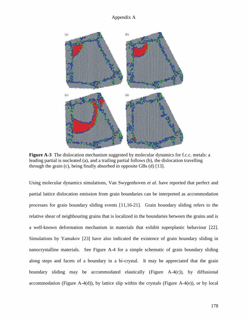
Appendix A
178
Figure A-3 The dislocation mechanism suggested by molecular dynamics for f.c.c. metals: a
leading partial is nucleated (a), and a trailing partial follows (b), the dislocation travelling
through the grain (c), being finally absorbed in opposite GBs (d) [13].
Using molecular dynamics simulations, Van Swygenhoven et al. have reported that perfect and
partial lattice dislocation emission from grain boundaries can be interpreted as accommodation
processes for grain boundary sliding events [11,16-21]. Grain boundary sliding refers to the
relative shear of neighbouring grains that is localized in the boundaries between the grains and is
a well-known deformation mechanism in materials that exhibit superplastic behaviour [22].
Simulations by Yamakov [23] have also indicated the existence of grain boundary sliding in
nanocrystalline materials. See Figure A-4 for a simple schematic of grain boundary sliding
along steps and facets of a boundary in a bi-crystal. It may be appreciated that the grain
boundary sliding may be accommodated elastically (Figure A-4(c)), by diffusional
accommodation (Figure A-4(d)), by lattice slip within the crystals (Figure A-4(e)), or by local
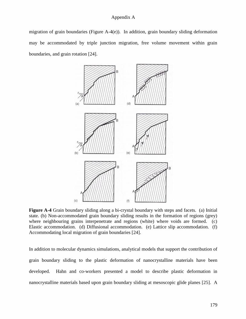
Appendix A
179
migration of grain boundaries (Figure A-4(e)). In addition, grain boundary sliding deformation
may be accommodated by triple junction migration, free volume movement within grain
boundaries, and grain rotation [24].
Figure A-4 Grain boundary sliding along a bi-crystal boundary with steps and facets. (a) Initial
state. (b) Non-accommodated grain boundary sliding results in the formation of regions (grey)
where neighbouring grains interpenetrate and regions (white) where voids are formed. (c)
Elastic accommodation. (d) Diffusional accommodation. (e) Lattice slip accommodation. (f)
Accommodating local migration of grain boundaries [24].
In addition to molecular dynamics simulations, analytical models that support the contribution of
grain boundary sliding to the plastic deformation of nanocrystalline materials have been
developed. Hahn and co-workers presented a model to describe plastic deformation in
nanocrystalline materials based upon grain boundary sliding at mesoscopic glide planes [25]. A
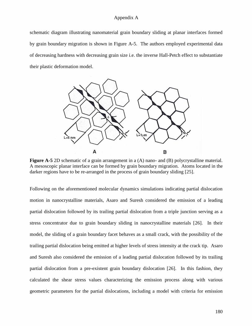
Appendix A
180
schematic diagram illustrating nanomaterial grain boundary sliding at planar interfaces formed
by grain boundary migration is shown in Figure A-5. The authors employed experimental data
of decreasing hardness with decreasing grain size i.e. the inverse Hall-Petch effect to substantiate
their plastic deformation model.
Figure A-5 2D schematic of a grain arrangement in a (A) nano- and (B) polycrystalline material.
A mesoscopic planar interface can be formed by grain boundary migration. Atoms located in the
darker regions have to be re-arranged in the process of grain boundary sliding [25].
Following on the aforementioned molecular dynamics simulations indicating partial dislocation
motion in nanocrystalline materials, Asaro and Suresh considered the emission of a leading
partial dislocation followed by its trailing partial dislocation from a triple junction serving as a
stress concentrator due to grain boundary sliding in nanocrystalline materials [26]. In their
model, the sliding of a grain boundary facet behaves as a small crack, with the possibility of the
trailing partial dislocation being emitted at higher levels of stress intensity at the crack tip. Asaro
and Suresh also considered the emission of a leading partial dislocation followed by its trailing
partial dislocation from a pre-existent grain boundary dislocation [26]. In this fashion, they
calculated the shear stress values characterizing the emission process along with various
geometric parameters for the partial dislocations, including a model with criteria for emission
Appendix A
181
from the grain boundary. However, as pointed out later by Van Swygenhoven [13], partial
dislocation emission is only one component of the complete mechanism by which plastic flow
may be carried in nanocrystalline materials, and that propagation and absorption of the
aforementioned dislocations must be properly considered as well. In other words, the nucleation
of a partial dislocation must be considered as a separate process from its propagation within the
grain. Indeed, partials are often observed to nucleate but not propagate, remaining for a while as
extrinsic grain boundary dislocation segments that perform a number of attempts to propagate
[13]. The interaction of a propagating dislocation with a grain boundary therefore appears to be
very dependent on the structure of that grain boundary.
Moreover, due to the intense interaction between the grain boundary and the dislocations, the
grain boundary structure is continuously changing, which in some cases also results in grain
boundary migration and associated coarsening of a grain at the expense of its neighboring grain
[13], as depicted in Figure A-4(f). Consequently, while the specific mechanisms of dislocation
emission from grain boundaries have received focused attention over the past 10 years, the
continuously changing structure of the nanomaterial grain boundary and how it influences the
motion of the dislocations with which it interacts (including pinning and de-pinning) has made
the task of accurately simulating such events extremely challenging. In other words, it is not yet
possible to understand the complex dynamic process of grain boundary sliding by analytical
modeling as the process is associated with the evolution, annihilation, and mutual interaction of
various defect structures in the process [27]. Nevertheless, the analytical modeling framework to
describe grain boundary sliding and its concomitant accommodation processes as carriers of
plastic flow in nanocrystalline materials remains in development [e.g. 28-32]
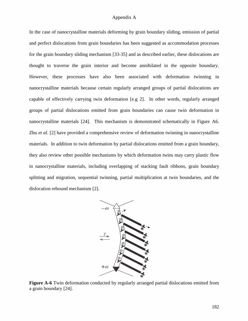
Appendix A
182
In the case of nanocrystalline materials deforming by grain boundary sliding, emission of partial
and perfect dislocations from grain boundaries has been suggested as accommodation processes
for the grain boundary sliding mechanism [33-35] and as described earlier, these dislocations are
thought to traverse the grain interior and become annihilated in the opposite boundary.
However, these processes have also been associated with deformation twinning in
nanocrystalline materials because certain regularly arranged groups of partial dislocations are
capable of effectively carrying twin deformation [e.g 2]. In other words, regularly arranged
groups of partial dislocations emitted from grain boundaries can cause twin deformation in
nanocrystalline materials [24]. This mechanism is demonstrated schematically in Figure A6.
Zhu et al. [2] have provided a comprehensive review of deformation twinning in nanocrystalline
materials. In addition to twin deformation by partial dislocations emitted from a grain boundary,
they also review other possible mechanisms by which deformation twins may carry plastic flow
in nanocrystalline materials, including overlapping of stacking fault ribbons, grain boundary
splitting and migration, sequential twinning, partial multiplication at twin boundaries, and the
dislocation rebound mechanism [2].
Figure A-6 Twin deformation conducted by regularly arranged partial dislocations emitted from
a grain boundary [24].
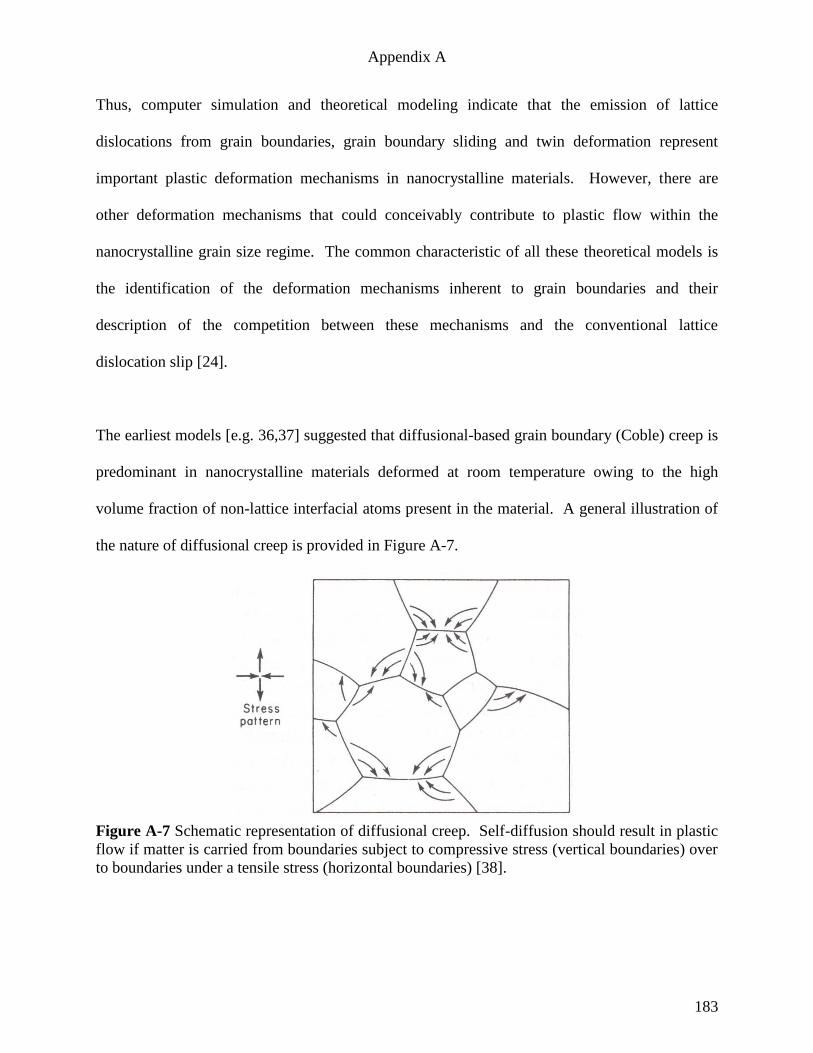
Appendix A
183
Thus, computer simulation and theoretical modeling indicate that the emission of lattice
dislocations from grain boundaries, grain boundary sliding and twin deformation represent
important plastic deformation mechanisms in nanocrystalline materials. However, there are
other deformation mechanisms that could conceivably contribute to plastic flow within the
nanocrystalline grain size regime. The common characteristic of all these theoretical models is
the identification of the deformation mechanisms inherent to grain boundaries and their
description of the competition between these mechanisms and the conventional lattice
dislocation slip [24].
The earliest models [e.g. 36,37] suggested that diffusional-based grain boundary (Coble) creep is
predominant in nanocrystalline materials deformed at room temperature owing to the high
volume fraction of non-lattice interfacial atoms present in the material. A general illustration of
the nature of diffusional creep is provided in Figure A-7.
Figure A-7 Schematic representation of diffusional creep. Self-diffusion should result in plastic
flow if matter is carried from boundaries subject to compressive stress (vertical boundaries) over
to boundaries under a tensile stress (horizontal boundaries) [38].
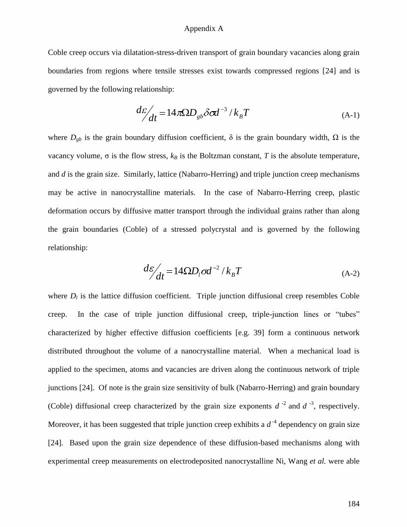
Appendix A
184
Coble creep occurs via dilatation-stress-driven transport of grain boundary vacancies along grain
boundaries from regions where tensile stresses exist towards compressed regions [24] and is
governed by the following relationship:
TkdDdt
dBgb /14 3
(A-1)
where Dgb is the grain boundary diffusion coefficient, δ is the grain boundary width, Ω is the
vacancy volume, σ is the flow stress, kB is the Boltzman constant, T is the absolute temperature,
and d is the grain size. Similarly, lattice (Nabarro-Herring) and triple junction creep mechanisms
may be active in nanocrystalline materials. In the case of Nabarro-Herring creep, plastic
deformation occurs by diffusive matter transport through the individual grains rather than along
the grain boundaries (Coble) of a stressed polycrystal and is governed by the following
relationship:
TkdDdt
dBl /14 2
(A-2)
where Dl is the lattice diffusion coefficient. Triple junction diffusional creep resembles Coble
creep. In the case of triple junction diffusional creep, triple-junction lines or “tubes”
characterized by higher effective diffusion coefficients [e.g. 39] form a continuous network
distributed throughout the volume of a nanocrystalline material. When a mechanical load is
applied to the specimen, atoms and vacancies are driven along the continuous network of triple
junctions [24]. Of note is the grain size sensitivity of bulk (Nabarro-Herring) and grain boundary
(Coble) diffusional creep characterized by the grain size exponents d -2
and d
-3, respectively.
Moreover, it has been suggested that triple junction creep exhibits a d -4
dependency on grain size
[24]. Based upon the grain size dependence of these diffusion-based mechanisms along with
experimental creep measurements on electrodeposited nanocrystalline Ni, Wang et al. were able
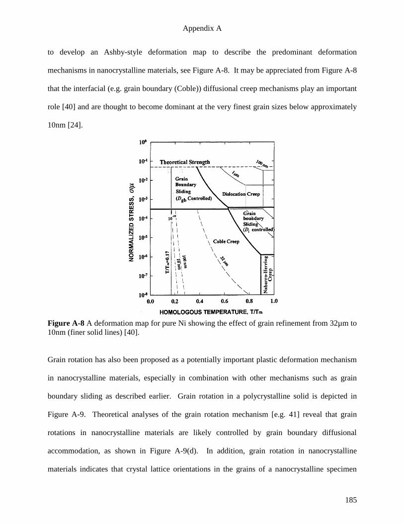
Appendix A
185
to develop an Ashby-style deformation map to describe the predominant deformation
mechanisms in nanocrystalline materials, see Figure A-8. It may be appreciated from Figure A-8
that the interfacial (e.g. grain boundary (Coble)) diffusional creep mechanisms play an important
role [40] and are thought to become dominant at the very finest grain sizes below approximately
10nm [24].
Figure A-8 A deformation map for pure Ni showing the effect of grain refinement from 32µm to
10nm (finer solid lines) [40].
Grain rotation has also been proposed as a potentially important plastic deformation mechanism
in nanocrystalline materials, especially in combination with other mechanisms such as grain
boundary sliding as described earlier. Grain rotation in a polycrystalline solid is depicted in
Figure A-9. Theoretical analyses of the grain rotation mechanism [e.g. 41] reveal that grain
rotations in nanocrystalline materials are likely controlled by grain boundary diffusional
accommodation, as shown in Figure A-9(d). In addition, grain rotation in nanocrystalline
materials indicates that crystal lattice orientations in the grains of a nanocrystalline specimen
Appendix A
186
move to minimize the grain boundary energy, depending on the boundary misorientation
parameters [24]. As described earlier, the TEM observations of Wang et al. [8] indicated a grain
rotation and coalescence mechanism. Hence, in these circumstances, plastic deformation in
nanocrystalline materials essentially changes the structure of the grain boundaries themselves. In
this context, the connections between imposed plastic deformation in nanocrystalline materials
and the resultant changes in grain boundary structures due to the aforementioned grain boundary
diffusion, emission and absorption of lattice dislocation at grain boundaries, grain boundary
sliding, and grain rotation are currently a matter of intense debate and could potentially be
greatly assisted by the development of an analytical technique to measure grain boundary
structure in nanocrystalline materials, similar to the Orientation Imaging Microscopy capability
available for such study in coarse-grained materials.
Figure A-9 Grain rotation in a polycrystalline solid. (a) Initial state. (b) Non-accommodated
grain rotation results in the formation of small regions (black regions near boundaries of rotated
grain) where neighbouring grains interpenetrate and small regions (white regions near
boundaries of rotated grain) where voids are formed. (c) Accommodation by bulk diffusion. (d)
Accommodation by grain boundary diffusion [24].
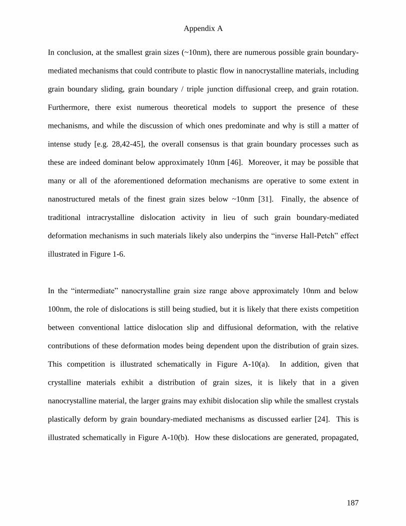
Appendix A
187
In conclusion, at the smallest grain sizes (~10nm), there are numerous possible grain boundary-
mediated mechanisms that could contribute to plastic flow in nanocrystalline materials, including
grain boundary sliding, grain boundary / triple junction diffusional creep, and grain rotation.
Furthermore, there exist numerous theoretical models to support the presence of these
mechanisms, and while the discussion of which ones predominate and why is still a matter of
intense study [e.g. 28,42-45], the overall consensus is that grain boundary processes such as
these are indeed dominant below approximately 10nm [46]. Moreover, it may be possible that
many or all of the aforementioned deformation mechanisms are operative to some extent in
nanostructured metals of the finest grain sizes below ~10nm [31]. Finally, the absence of
traditional intracrystalline dislocation activity in lieu of such grain boundary-mediated
deformation mechanisms in such materials likely also underpins the “inverse Hall-Petch” effect
illustrated in Figure 1-6.
In the “intermediate” nanocrystalline grain size range above approximately 10nm and below
100nm, the role of dislocations is still being studied, but it is likely that there exists competition
between conventional lattice dislocation slip and diffusional deformation, with the relative
contributions of these deformation modes being dependent upon the distribution of grain sizes.
This competition is illustrated schematically in Figure A-10(a). In addition, given that
crystalline materials exhibit a distribution of grain sizes, it is likely that in a given
nanocrystalline material, the larger grains may exhibit dislocation slip while the smallest crystals
plastically deform by grain boundary-mediated mechanisms as discussed earlier [24]. This is
illustrated schematically in Figure A-10(b). How these dislocations are generated, propagated,
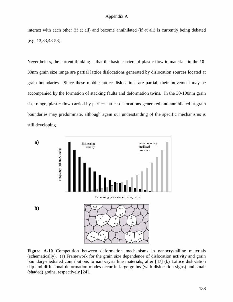
Appendix A
188
interact with each other (if at all) and become annihilated (if at all) is currently being debated
[e.g. 13,33,48-58].
Nevertheless, the current thinking is that the basic carriers of plastic flow in materials in the 10-
30nm grain size range are partial lattice dislocations generated by dislocation sources located at
grain boundaries. Since these mobile lattice dislocations are partial, their movement may be
accompanied by the formation of stacking faults and deformation twins. In the 30-100nm grain
size range, plastic flow carried by perfect lattice dislocations generated and annihilated at grain
boundaries may predominate, although again our understanding of the specific mechanisms is
still developing.
Figure A-10 Competition between deformation mechanisms in nanocrystalline materials
(schematically). (a) Framework for the grain size dependence of dislocation activity and grain
boundary-mediated contributions to nanocrystalline materials, after [47] (b) Lattice dislocation
slip and diffusional deformation modes occur in large grains (with dislocation signs) and small
(shaded) grains, respectively [24].
a)
b)
Appendix A
189
A.4 References
[1] W.W. Milligan, S.A. Hackney, M. Ke, E.C. Aifantis, Nanostr. Mater. 2 (1993) 267.
[2] Y.T. Zhu, X.Z. Liao, X.L. Wu, Prog. Mater. Sci. 57 (2012) 1.
[3] M. Ke, S.A. Hackney, W.W. Milligan, E.C. Aifantis, Nanostr. Mater. 5, 6 (1995) 689.
[4] C.J. Youngdahl, J.R. Weertman, R.C. Hugo, H.H. Kung, Scripta Mater. 44 (2001) 1475.
[5] K.S. Kumar, S. Suresh, M.F. Chisholm, J.A. Horton, P. Wang, Acta Mater. 51 (2003) 387.
[6] Z. Shan, E.A. Stach, J.M.K. Wiezorek, J.A. Knapp, D.M. Follstaedt, S.X. Mao, Science 305
(2004) 654.
[7] M. Jin, A.M. Minor, E.A. Stach, J.W. Morris, Acta Mater. 52 (2004) 5381.
[8] Y.B. Wang, B.Q. Li, M.L. Sui, S.X. Mao, Appl. Phys. Lett. 92 (20080 011903.
[9] Z. Budrovic, H. Van Swygenhoven, P.M. Derlet, S. Van Petegem, B. Schmitt, Science 304
(2004) 273.
[10] G.J. Fan, L.F. Fu, Y.D. Wang, Y. Ren, H. Choo, P.K. Liaw, G.Y. Wang, N.D. Browning,
Appl. Phys. Lett. 89 (2006) 101918.
[11] D. Wolf, V. Yamakov, S.R. Philpot, A. Mukherjee, H. Gleiter, Acta Mater. 53 (2005) 1.
[12] H. Van Swygenhoven, P.M. Derlet, A. Hasnaoui, M. Samaras, in Nanostructures: Synthesis,
Functional Properties and Applications, T. Tsakalakos et al. (eds.), Kluwer (2003).
[13] H. Van Swygenhoven, Mater. Sci. Eng. A 483-484 (2008) 33.
[14] V. Yamakov, D. Wolf, S.R. Phillpot, H. Gleiter, Acta Mater. 50, 1 (2002) 61.
[15] M. Chen, E. Ma, K.J. Hemker, H. Sheng, Y. Wang, X. Cheng, Science 300 (2003) 1275.
[16] J. Schiotz, Scripta Mater. 51 (2004) 837.
[17] J. Schiotz, F.D. Di Tolla, K.W. Jacobsen, Nature 391 (1998) 561.
[18] J. Schiotz, T. Vegge, F.D. Di Tolla, K.W. Jacobsen, Phys. Rev. B 60 (1999) 11971.
Appendix A
190
[19] H. Van Swygenhoven, M. Spaczer, A. Caro, Acta Mater. 47, 10 (1999) 3117.
[20] H. Van Swygenhoven, M. Spaczer, A. Caro, D. Farkas, Phys. Rev. B 60 (1999) 22.
[21] H. Van Swygenhoven, P.M. Derlet, Phys. Rev. B 64 (2001) 224105.
[22] A.V. Sergueeva, N.A. Mara, N.A. Krasilnikov, R.Z. Valiev, A.K. Mukherjee, Phil. Mag.
86,36 (2006) 5797.
[23] V. Yamakov, D. Wolf, S.R. Phillpot, A.K. Mukherjee, H. Gleiter, Nature Mater. 3 (2004)
43.
[24] I. A Ovid’ko, in Structural Nanocrystalline Materials, ed. C.C. Koch et al, Cambridge
University Press, Cambridge, UK (2007), Chapter 5.
[25] H. Hahn, P. Mondal, K.A. Padmanabhan, Nanostr. Mater. 9 (1997) 603.
[26] R.J. Asaro, S. Suresh, Acta Mater. 53 (2005) 3369.
[27] S.H. Whang (ed.), Nanostructured Metals and Alloys: Processing, Microstructure,
Mechanical Properties and Applications, Woodhead Pub., Cambridge, UK (2011).
[28] M. Yu. Gutkin, I.A. Ovid’ko, N.V. Skiba, Acta Mater. 51 (2003) 4059.
[29] M. Yu. Gutkin, I.A. Ovid’ko, N.V. Skiba, Phys. Solid State. 47 (2005) 1662.
[30] S.V. Bobylev, I.A. Ovid’ko, Appl. Phys. Lett. 92 (2008) 081914.
[31] I.A. Ovid’ko, A.G. Sheinerman, Acta Mater. 57 (2009) 217.
[32] I.A. Ovid’ko, A.G. Sheinerman, N.V. Skiba, Acta Mater. 59 (2011) 678.
[33] X.L. Wu, Y.T. Zhu, Y.G. Wei, Q. Wei, Phys. Rev. Lett. 103 (2009) 205504.
[34] H. Van Swygenhoven, P. M. Derlet, Phys. Rev. B 66 (2002) 24101.
[35] V. Yamakov, D. Wolf, S.R. Phillpot, A.K. Mukherjee, H. Gleiter, Nature Mater. 1 (2002)
45.
[36] H. Gleiter, Prog. Mat. Sci., 33 (1989) 223..
Appendix A
191
[37] A.H. Chokshi, A. Rosen, J. Karch, H. Gleiter, Scripta Mater., 25 (1989) 641.
[38] R.E. Reed-Hill, R. Abbaschian, Physical Metallurgy Principles, third ed., PWS Pub.,
Boston, MA (1994) 159.
[39] D.M. Doyle, G. Palumbo, K.T. Aust, A.M. El-Sherik, U. Erb, Acta Metall. Mater. 43, 8
(1995) 3027.
[40] N. Wang, Zhirui Wang, K.T. Aust, U. Erb, Mater. Sci. Eng. A 237 (1997) 150.
[41] A.J. Haslam, S.R. Philpott, D. Wolf, D. Moldovan, H. Gleiter, Mater. Sci. Eng. A 318
(2001) 293.
[42] X.L. Wu, Y.T. Zhu, Appl. Phys. Lett. 89 (2006) 031922.
[43] K.A. Padmanabhan, G.P. Dinda, H. Hahn, H. Gleiter, Mater. Sci. Eng. A 452-453 (2007)
462.
[44] R.A. Vandermeer, N. Hansen, Acta Mater. 56 (2008) 5719.
[45] O. Bouaziz, Y. Estrin, Y. Brechet, J.D. Embury, Scripta Mater. 63 (2010) 477.
[46] J. Weismueller, J. Markmann, Adv. Eng. Mater. 7,4 (2005) 202.
[47] C. Suryanarayana, J. Singh, F.H. Froes (eds.), Processing and Properties of Nanocrystalline
Materials, TMS, Warrendale, PA (1995) 1.
[48] G. Saada, Mat. Sci. Eng. A400-401 (2005) 146.
[49] C.E. Carlton, P.J. Ferreira, Acta Mater. 55 (2007) 3749.
[50] M. Yu. Gutkin. I.A. Ovid’ko, Appl. Phys. Lett. 88 (2006) 211901.
[51] L. Hollang, E. Hieckmann, D. Brunner, C. Holste, W. Skrotzki, Mater. Sci. Eng. A 424
(2006) 138.
[52] Y.J. Li, J. Mueller, H.W. Hoeppel, M. Goeken, W. Blum, Acta Mater. 55 (2007) 5708.
[53] A.V. Sergueeva, N.A. Mara, A.K. Mukherjee, Mater. Sci. Eng. A 463 (2007) 8.
Appendix A
192
[54] J. Rajagopalan, J.H. Han, M.T.A. Saif, Scripta Mater. 59 (2008) 921.
[55] G. Saada, Mater. Sci. Eng. A 483-484 (2008) 506.
[56] K. Lu, N. Hansen, Scripta Mater. 60 (2009) 1033.
[57] P. Gu, B.K. Kad, M. Dao, Scripta Mater. 62 (2010) 361.
[58] A. Godon, J. Creus, S. Cohendoz, E. Conforto, X. Feaugas, P. Girault, C. Savall, Scripta
Mater. 62 (2010) 403.


![Mechanical properties of solid bulk materials and thin films 1+2... · 2012-07-01 · Mechanical properties of solid bulk materials and thin films ... uniaxial tensile test [B]:](https://img.pdfslide.net/doc/110x75/5b4232157f8b9a66128b53d9/mechanical-properties-of-solid-bulk-materials-and-thin-films-12-2012-07-01.jpg)