Embed Size (px)
Citation preview

48 November 2006
One of the ways DDS differsfrom both phase locked loops
and mixing techniques is that the output is generated by a digital-to-analog (D/A) converter.There are four basic components toa DDS system:
1. Crystal oscillator2. Phase accumulator3. Look-up table4. D/A converter
The crystal oscillator defines thehighest frequency capable of beinggenerated by the system. The DDScovers an operating range limited bysampling theory (Shannon, Nyquist).The highest practical output frequen-cy is about 45% of the crystal oscil-lator frequency. One of the main
advantages of a DDS system is thatthe method of constructing theoutput signal is almost entirely digital, and the precise amplitude,frequency, and phase are knownand controlled at all times. Amongthe advantages of a DDS system are:
1. Very fine tuning steps2. Very fast switching time3. Phase continuous frequency
change4. Low phase noise
The November ‘05 issue ofQST had an article on a DDSdevice controlled by a PC. Afterreading it, I determined that itmight not be very difficult to build a stand-alone unit. I now have a DDS unit which is con-trolled by an RCM3610 by Rabbit
Semiconductor. The DDS unit hasthe following characteristics:
1. A two line LCD for a menu display2. Push button switches to step
through the menus3. Powered by a 7-15 VDC wall wart4. The following is programmable:
• Frequency in 1 Hz steps from 1 Hz to 10 MHz
• Phase• Wave form — sine, triangle,
square• PSK and FSK• Frequency sweep with pause• Amplitude of sine and triangle
waveforms
The system consists of twoprinted circuit boards. The first isthe main board with the processor,LCD, switch interfaces, and theDDS circuit. The second board hasthe programmable attenuator andoutput buffer.
There are three push buttonswitches in the design. Only two areused to navigate the menu system.PB3 is not used — it is available forfuture expansion. SW2 — a toggleswitch — is used when the PSK/FSK mode is selected. It is themethod of switching between thetwo frequencies and/or phases. This method allows you to put a connector in parallel with the switchin order to implement an externalmethod of control.
The Microprocessor
Refer to Figure 1. I chose theRCM3610 as the control device
STAND-ALONE
DDDDSS UUNNIITT
These photos show the DDS unit.
Direct DigitalSynthesis (DDS) is
one of the moreprevalent methodsused to generate a
frequency agilesignal today.
The material in thefollowing explanation wastaken from wwwwww..eehhbb..iittuu..
eedduu..ttrr//~~eeeeppaazzaarrcc//ddddssttuuttoorr..hhttmmll. If you want tosearch the Internet for
more information onDDS, I suggest you use
the full name as thesearch criteria otherwise
you will get lots of hitson dentistry!

mainly because I am quite familiarwith it. It is programmed in both Cand assembly language. It has quite afew parallel output bits, as well as several serial I/O ports. The parallelI/O is used for the LCD, switches, andChip Select signals.
Two resistor packs terminateunused inputs, as well as providingpullups for the switches. When themicroprocessor on the RCM3610comes out of its reset state, all of theI/O pins which can be inputs are setas inputs. All inputs on a CMOSdevice should be terminated to eitherground or VDD. Floating inputs cancause localized damage to the device.
The interface to the LCD uses afeature of the processor which allowsyou to expand the parallel I/O capa-
bility by up to 64K bytes. This featureenables the program to access theexternal devices in essentially thesame way as you would access theinternal parallel I/O ports. Parallel PortA becomes the data bus, Parallel PortB bits 2-7 become address bits, andbits from Parallel Port E are I/Ostrobes. Since I am never reading any-thing from the LCD, its interface onlyneeds to use a single address bit (PB2)in order to select between either thecontrol register or the data register.
The interface to both the DDSand attenuator ICs use SPI (SerialPeripheral Interface). This is a relative-ly high speed serial communicationsmethod which is used by manyperipheral ICs. You will find manyother ICs which use it — A/Ds, D/As,
memories, etc. The April ‘06 issue ofNV has a good article discussing SPI.
In the general case, each ICrequires four signals: Clock, Data In,Data Out, and Chip Select. Neither ofthe SPI devices in this system sends anydata back to the processor so they donot have a Data Out. Each device musthave its own Chip Select, the other signals are shared. Only the device withthe active Chip Select will communi-cate with the controlling processor.
The LCD
The LCD has an S6A0069 controller which is compatible withthe industry standard HD44780. Ichose to use the four-bit interface tothe LCD because I eventually want to
BY LARRY CICCHINELLI
November 2006 49
9834 DDS with
RCM3610 Controller
VDD
SCLK
PG6
VDD
EN
SDI
DB2
DB1
DB0
DB3
/CS
LCDPD5
FSK/PSK
Processor LCD
S2
H4 S4
C4
1000pf
H2
IC1 RCM3610
IC2
LC
MS
-S0
16
02
PB
1
PB
2
PB
3
RNET1 10K
RNET2 10K
Sw
2
RS
PF0
PF1
1 2 3 4 5
PA71
PA53
PA35
PA17
PF19
PB011
PB313
PB515
PF417
PF619
PC021
PC223
PE725
PE427
PE029
PG631
/IORD33
PD535
VBAT37
+5V39
GND40
GND38
/RES36
PD434
/IOWR32
PG730
PE128
PE526
PC3/PG324
PC1/PG222
PF720
PF518
PB716
PB414
PB212
PF010
PA08
PA26
PA44
PA62
VSS1
blank2
VDD3
Vo4
RS5
R/W6
E7
DB08
DB19
DB210
DB311
DB412
DB413
DB614
DB715
A16
K17
1
1
1
2
3
4
5
6
7
8
9
10
123456789
10
FIGURE 1
try to build the device using a low pin-count PIC. You can see from theschematic that there are two controllines being used: Enable and RegisterSelect. The Control Strobe from Port Ebit 1 is set up as a Write Strobe todrive the Enable input. The RegisterSelect is driven from Port B bit 2which is I/O address bit 0. I am notusing the read capability so I have theRead/Write grounded to permanentlyenable its Write operation.
I chose a two-line, 16 characterdevice in order to get a low-cost
display. I also wanted to choose anLCD which can be easily obtained byanyone who wants to build the unit.However, I have since found sometwo-line, 20 character LCDs which arerelatively inexpensive. For those whowant to enhance the menu system, itwould be fairly easy to use a four-lineLCD instead. The pin-out for mostcharacter LCDs is common so you can probably use almost any unit, aslong as it uses an HD44780, or equivalent, and is at least two lines of16 characters each.
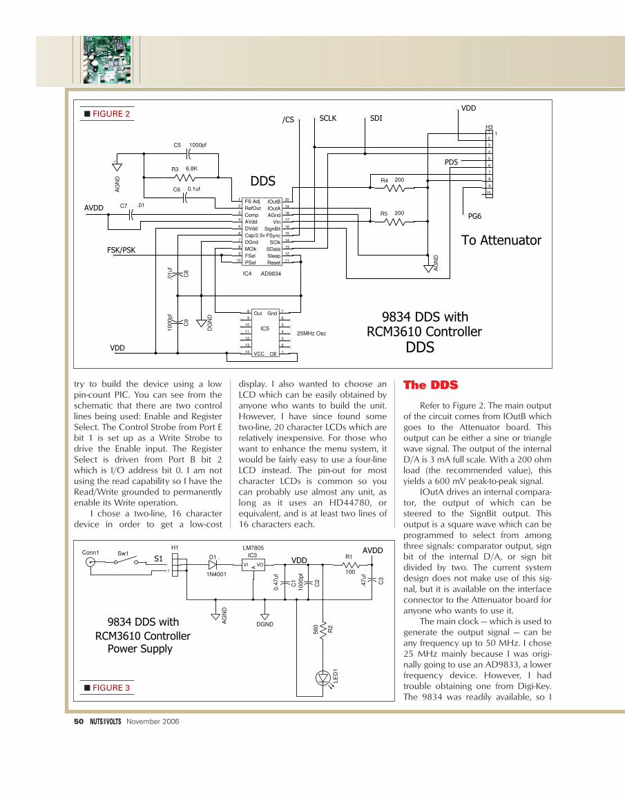
The DDS
Refer to Figure 2. The main outputof the circuit comes from IOutB whichgoes to the Attenuator board. This output can be either a sine or trianglewave signal. The output of the internalD/A is 3 mA full scale. With a 200 ohmload (the recommended value), thisyields a 600 mV peak-to-peak signal.
IOutA drives an internal compara-tor, the output of which can besteered to the SignBit output. This output is a square wave which can beprogrammed to select from amongthree signals: comparator output, signbit of the internal D/A, or sign bitdivided by two. The current systemdesign does not make use of this sig-nal, but it is available on the interfaceconnector to the Attenuator board foranyone who wants to use it.
The main clock — which is used togenerate the output signal — can beany frequency up to 50 MHz. I chose25 MHz mainly because I was origi-nally going to use an AD9833, a lowerfrequency device. However, I hadtrouble obtaining one from Digi-Key.The 9834 was readily available, so I
50 November 2006
To Attenuator
9834 DDS withRCM3610 Controller
DDS
FSK/PSK
SCLK SDI
DDS
VDD
PD5
AVDD
VDD
PG6
/CS
C5 1000pf
C6 0.1uf
C7 .01
C8
.01
uf
C9
10
00
pf
H3
IC4 AD9834
IC525MHz Osc
DG
ND
AG
ND
AG
ND
R3 6.8K
R4 200
R5 200
11
2
3
4
5
6
7
8
9
10
FS Adj1
RefOut2
Comp3
AVdd4
DVdd5
Cap/2.5v6
DGnd7
MClk8
FSel9
PSel10
Reset11
Sleep12
SData13
SClk14
FSync15
SignBit16
VIn17
AGnd18
IOutA19
IOutB20
OE1
2
3
4
5
6Gnd
7Out
8
9
10
11
12
13
VCC14
1
VDD
AVDD
9834 DDS with
RCM3610 Controller
S1
Power Supply
AG
ND
C1
0.4
7uf
C2
1000pf
C3
.47uf
Conn1D1
1N4001
DGND
H1
IC3
LM7805
LE
D1
R1
100
R2
560
Sw1
1
VI
A
VO
FIGURE 2
FIGURE 3

changed my design to use it instead.The DDS can generate any fre-
quency up to one half the main clock(Fosc) in steps of Fosc/228. This isbecause the DDS uses a 28 bit phaseaccumulator. With the 25 MHz oscil-lator, this yields steps of about 0.1 Hz.The highest practical sine wave outputis about 1 MHz. Higher frequency sig-nals do not look much like sine waves.
The Attenuator Board
My initial design did not have anymeans to control the amplitude of theoutput signal. I decided to implementan amplitude control circuit aftershowing my prototype to a fewfriends at work (Figure 4). The circuitconsists of three sections: an invertingamplifier to get the signal up to a high-er level, a programmable attenuator,and a voltage follower.
The inverting amplifier has a gain ofapproximately five — fixed by the ratioof R8/R7. Since the signal is applied tothe inverting input, I had to add an off-set circuit — R9 and R10 — to insure thatthe output signal stays in the linearrange of the op-amp. With these com-ponent values, the output voltageranges from about one volt to four volts.To keep the design simple, I decided tonot implement any kind of adjustments.
The attenuator con-sists of a programmablepotentiometer and voltagefollower. The AD5200 isprogrammable in 256equal steps with an end-to-end resistance of 10K. Theprogram allows you to setthe “wiper” to any of the256 positions. This yields astep size of 3V/256, orapproximately 12 mV. Itwould be fairly easy to mod-ify the program to allowyou to program in dB or mil-livolts. By changing the ratioof the gain resistors, youcan easily change the maxi-mum peak-to-peak voltage.If you change the gain, youwill need to change thevalue of at least one of the
offset resistors. An option which may beof interest is to make the maximum output voltage 0 dBm. When driving600 ohms, 0 dBm is 0.7746 volts. This isequivalent to about 2.19 volts peak-to-peak, which is very close to the outputvoltage of my circuit. By reducing thegain to a factor of 3.65 (instead of 5),you will get a maximum output voltageof 0 dBm. You might also then want tochange the output resistor (R11) from200 ohms to 600 ohms, so you have a600 ohm output impedance.
The Program
I have been using SPI devices formany years, but still managed to over-look a very important “feature” of SPI.There are four modes of SPI whichdefine various phase relationshipsbetween the clock and data signals.As it turns out, the DDS uses onemode and the attenuator IC uses a dif-ferent mode. At first, I did not realizethis — mainly due to not reading thespecs carefully enough. The programnow changes the SPI mode whenentering the attenuator function andthen restores it to the mode requiredby the DDS when exiting.
The main parts of program arecontained in two files: AD9834.C andAD9834.LIB. I also use a serial library
— FSER.LIB — for the SPI communica-tions. You will find that the source files(available on the Nuts & Volts websiteat www.nutsvolts.com) are fairly wellcommented and should be relativelyeasy to follow. Most of the code is in C but there are some functions partially in Assembly language.
The Menu
When not changing a parametervia the menu, the display will showthe current frequency and phase val-ues, as well as indicating the currentmode and waveform. There are notenough characters in the display Iused to also display the amplitude.
The menu system uses a two line,16 character-per-line LCD and twopush button switches. I found this to beadequate for my needs and it doesallow you to easily set up the unit.Following is a brief description of themenu and how to navigate it. The mainmenu consists of the following options:
1. F0 — Change Frequency 02. F1 — Change Frequency 13. P0 — Change Phase 04. P1 — Change Phase 15. Waveform6. Mode of Operation7. Amplitude
Stand-Alone DDS Unit
November 2006 51
VDD
VDD
S5
Amplifier and
Programmable Attenuator
IC7.1 AD8529
IC7.2 AD8529
IC7
.3
OP
27
9
IC8.1 AD5200
IC8
.2
AD
52
00
S3
R7 1K
R8 4.7K
R9 4.7K R10 680H5
R11 200
C11 0.47
C10 100pf
Conn2
GN
D
GN
D
GN
D
GN
D
-
+1
2
3
-
+7
6
5
V-4
V+8
/CS4
SDI5
CLK6
/SHDN7
VSS2
GND3
VDD8
B1
W9
A1
0
11
2
3
4
5
6
7
1
2
1
1
1
1
FIGURE 4

The Main menu is entered by pressing PB1. Generally,PB1 is used to step through the menu selections and PB2 isused to select the one you want. You can either hold PB1or press and release it. Each press and release will advanceto the next menu item. If you keep it pressed, the systemwill advance through the selections at one-second intervals.The menu will wrap around to the first item if you hold the switch past the last one. Pressing PB2 — after releasingPB1 -— tells the system to select the currently displayedmenu item.
For the Frequency, Phase, and Amplitude selections,the current value will be displayed and the cursor will beplaced on the most significant digit. Press and release PB1to advance the cursor to the next digit. Holding PB1 willcause the cursor to continue to advance through the digitswith a one second delay between each until PB1 isreleased. Once the cursor is on the digit you want tochange, just press and release — or press and hold — PB2until the desired digit value is displayed. Using PB1 toadvance past the last digit will cause the displayed value tobe programmed into the system when PB1 is finallyreleased.
The Waveform and Mode menu operations are similarto the Main menu operation. PB1 is used to step throughthe available options. PB2 is used to select the desiredoption.
The values in () are what shows in the status display.The Waveform menu has the following options:
1. Reset (RE) — Turns the output off2. Sine (SI) — Sine wave3. Triangle (TR) — Triangle wave4. Square (SQ) — Square wave the same as the selected
frequency5. Square/2 (S2) — Square wave generated by the sign bit of the
D/A, effectively half of the frequency
The Mode menu has these options:
1. CW-F0 (CW) — Continuous wave of F0 and Phase 02. CW-F1 (CW) — Continuous wave of F1 and Phase 13. FSK/PSK (FS) — Enable FSK/PSK using SW2 or an external
switch4. Ramp 1 (R1) — Ramp from F0 up to F1, jump back to F0 and
start over5. Ramp 2 (R2) — Ramp from F0 up to F1, then ramp down to
F0 and start over
For the Ramp modes, you are asked to enter both a step size and a delay value. The step size is in 1 Hzincrements. The delay is in one millisecond increments upto 99 seconds. You can pause the Ramp at any time bypressing PB2. When paused, the LCD will show the currentfrequency of the ramp. Press PB2 again to proceed withthe ramp. Pressing PB1 terminates the ramp process.
Construction Hints
The total cost of the parts is about $100. I canprogram the RCM3610 if you do not have theappropriate tools. All I ask is that you send me onealong with return postage.
The two PCBs (printed circuit boards) can bepurchased from FAR Circuits (FARcircuits.net) for$14 for the pair. They do not do plated-throughholes, so you will have to insert some jumpers atthe appropriate locations. You can find a completeset of PCB files (including the Gerber and drill files) on my website at www.qsl.net/k3pto.
There are no critical circuits in this design. Idesigned the boardso that the outputof the 25 MHzoscillator has a veryshort run to theDDS IC. In mostcases, the resistorvalues are not critical. If you wanta more exact out-put level, you maywant to calculatebetter values forR4, R7, and R8 (seethe text).
52 November 2006
PARTS LIST This indicates where I purchased the major parts. You can probably find equivalent parts from other vendors and possiblysave some money in shipping costs.
LOC PART NO. QTY VENDOR Circuit Boards 1 Far Circuits PB1,2,3 26622CK 3 Jameco Sw1,2 72160CK 2 Jameco RNET1, RNET2 24643CK 2 Jameco IC1 RCM3610 1 *Rabbit Socket for IC1 S7123-ND 1 Digi-Key IC2 (LCD) 67-1768-ND 1 Digi-Key IC3 (7805) 51262CK 1 Jameco IC4 (DDS) AD9834BRU-ND 1 Digi-Key IC5 (Osc) SE1714-ND 1 Digi-Key IC7 (Op-amp) AD8529AR-ND 1 Digi-Key IC8 (Potentiometer) AD5200BRM10-ND 1 Digi-Key H1,2,3,4,5 103341CK 2 Jameco D1 35975CK 1 Jameco LED1 333877CK 1 Jameco S1,2,4,5 103157CK 2 Jameco Pins for S1,2,4,5 100765CK 45 Jameco S3 S4107-ND 1 Digi-Key Conn1 (2.5 mm) 202358CK 1 Jameco Mate for Conn1 190537CK 1 Jameco Conn2 (RCA) 159484CK 1 Jameco Mate for Conn2 229921CK 1 Jameco Box (6x4x2) 270-1806 1 RadioShack
*Rabbit Semiconductor — wwwwww..rraabbbbiitt..ccoomm
All resistors are 1/4 watt, 5% R1 100Ω R2 560Ω R3 6.8K R4,R5,R11 200Ω R7 1K R8,R9 4.7K R10 680Ω
All capacitors are mono-lithic ceramic C1,C3,C11 0.47 µF C2,C4,C5,C9 1,000 pf C6 0.1 µF C7,C8 0.01 µF C10 100 pf
Working with SMD ICs can be achallenge, especially the attenuatorIC. I strongly recommend that youhave a soldering iron with a verysmall tip and some very thin solder.You should also work using a lamp with a magnifying lens. I have alamp with a 3X magnifying lens, butsometimes wish it were 5X. Whensoldering the SMD ICs, the method I use is:
• Tin the pads on the PCB — makesure there are no solder bridges!
• Align the IC on the pads makingsure ALL the leads line up.
• Use a strip of plastic electrical tape,cut thin, to fasten it in place.
• Use very thin solder and an ironwith a very thin tip to solder it.
• Use solder wick to remove any sol-der bridges.
You do not have to use the samemethod of construction as I did withthe headers and sockets. I preferthem so that I can easily take apartthe system pieces. You can solderwires directly to the PCB instead ofusing any of the header/socket pairs.If you do use the connectors, you willneed to have either a crimp tool forthe pins or a pair of small needle-nose pliers to use. I used pliers anddid not have any trouble. Both theheaders and sockets need to be cutto size. This can be done easily witha utility knife.
I cut the opening for the LCDusing a Dremel tool. As it turns out, Icut my opening larger than requiredbecause I wanted the LCD to beclose to the top surface of the box.
You may need to drill a newmounting hole for the voltage regulator. Some 7805s are differentsizes with the hole further from thepins. I did not use a heatsink, but youcan if you wish — there is room for asmall one.
The crystal oscillator has pin 1closest to the edge of the board.
Make sure you solder bothsides of the components whichhave PC traces on the top. It helps if you do not mount the leaded components right upagainst the PCB.
When mounting the sockets,make sure you do NOT mountthem right up against the PCB sothat you can solder the pins whichhave connections on the top side.
I soldered 6” wires onto theLED and then soldered the wires tothe PCB. This allows you to mountthe LED just about anywhere onthe cover. Try to drill the mountinghole just large enough for the bodyof the LED and not so large that itallows the bottom lip to pass through.I usually use Goop to glue LEDs to aplastic lid.
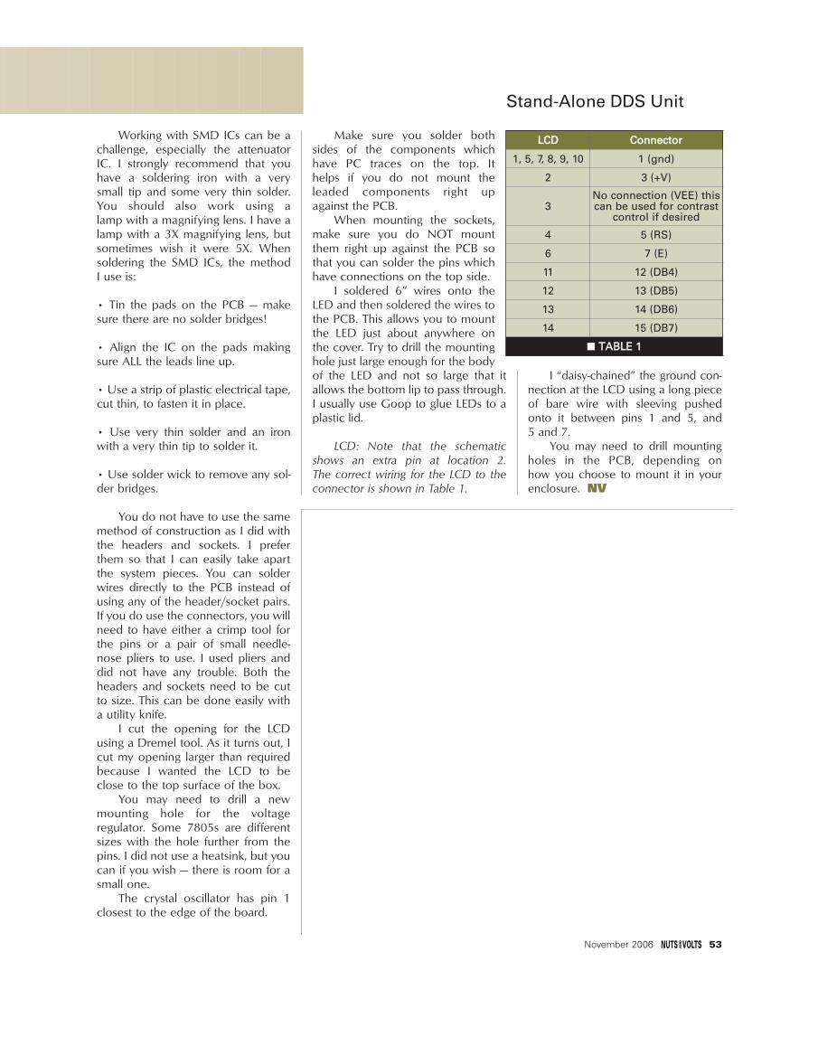
LCD: Note that the schematicshows an extra pin at location 2. The correct wiring for the LCD to theconnector is shown in Table 1.
I “daisy-chained” the ground con-nection at the LCD using a long pieceof bare wire with sleeving pushedonto it between pins 1 and 5, and 5 and 7.
You may need to drill mountingholes in the PCB, depending on how you choose to mount it in yourenclosure. NV
Stand-Alone DDS Unit
November 2006 53
LLCCDD CCoonnnneeccttoorr
1, 5, 7, 8, 9, 10 1 (gnd)
2 3 (+V)
3No connection (VEE) thiscan be used for contrast
control if desired
4 5 (RS)
6 7 (E)
11 12 (DB4)
12 13 (DB5)
13 14 (DB6)
14 15 (DB7)
TTAABBLLEE 11