Embed Size (px)
Citation preview

464 IEEE TKANSACTIONS ON CIRCUITS AND SYSTEMS, VOL. 37, NO. 4, APRIL 1990
Synthesis of Arbitrary Rational Transfer Functions in S Using Uniform Distributed
RC Active Circuits
Ahsrracf -This paper describes a synthesis technique whereb! network functions that are rational in c are realized with uniform distributed R C elements and active elements. In contrast to previous distributed s?nthesis approaches, the technique works directly in the s plane without complex mathematical transformations, uses on11 grounded rectangular single-la) er uniform distributed RC structures, and can realize man! network topolo- gies. Classical approximation functions, such as Butternorth and Chebj - chev, and well-known filter topologies can be used. Experimental results for a band-pass biquad are presented, and practical implementation possi- bilities are discussed.
I. INTRODUCTION
LTHOUGH the synthesis of distributed RC net- A works received considerable attention in the 1960’s and 1970’s, active filter implementations today are based almost exclusively on lumped-circuit synthesis theory. However, distributed filter implementations have several inherent advantages. First, from a network theory view- point, a distributed network is more general and versatile than a lumped one. A n e t w e composed of uniform distributed RC structures (URC) can realize either an infinite number of poles and zeros, or a finite number& poles and zeros exactly as a lumped network. Second, URC implementations consist of structures that contain both the resistance and capacitance needed for active filters. Since the distributed resistance and capacitance are physically co-located, the area needed to realize RC products is in many circumstances reduced, saving fabrication costs. Third, many “lumped” implementations have distributed parasitic capacitances and resistances that are not always negligible. Whether a parallel plate capacitor is imple- mented in thin-film or metal-oxide semiconductor (MOS) technology, the resistance of the plates is nonzero and m q degrade circuit performance in some instances. Such a distributed resistance makes the “capacitor” appear as a uRC structure. Similarly, a resistance structure in many technologies will have a distributed capacitance to another
Manuscript received August 29, 1988; revised May 1989. This work was supported in part the National Science Foundation under <;rant MIP-86-16394. This paper was recommended by Associate Editor. J Mavor.
J . M. Khoury is with AT&T Bell Laboratories. Murra! Hill. NJ 07974 Y. P. Tsividis is with the Department of E.lectrica1 Engineering and the
Center for Telecommunications Research. (‘olumbia Universit). Ne\\ York. N Y 10027.
IEEE Log Number 8933897.
circuit node. Rather than considering distributed effects as nonidealities in the various implementations, they can be incorporated into the synthesis process and used to advan- tage.
An early synthesis technique for U= networks is given in [l]. It realizes the network function with commensurate (i.e., same length) U= structures. The distributed network function is transformed with the Wyndrum transforma- tion, yielding a network function in the transformed plane that is positive real in the new frequency variable. The transformed network function is then synthesized using classical lumped LC synthesis techniques. After the lumped synthesis is complete, all inductors are replaced with short-circuited U E stubs and all capacitors are replaced with open-circuited stubs. Wyndrum’s approach is appeal- ing from a network theory viewpoint; however, it has several difficulties and restrictions that limit its usefulness. The major weakness is that the network function must be expressed as a ratio of two polynomials in P, the trans- formed frequency variable. The filter approximation prob- lem, determining the two polynomials, is described in [l], but is not as well developed as classical approximation methods [ 2 ] , [3]. The second weakness is that the network functions that can use Wyndrum’s transformation wlule resulting in a positive real function represent a restricted class of distributed U= networks. Another researcher [4] has conceived a different transformation; however, it has restrictions as does Wyndrum’s transformation.
Several researchers have conceived of ways in which distributed circuits can be used to realize network functions that are rational in s. References [ 5 ] , [6] achieve rational functions by changing the E line structure to contain additional layers and/or tapering the line. The approaches are complex mathematically and not practical to realize in common technologies. Reference [7] has built on the method in [ 5 ] to achieve the synthesis of active open-circuit transfer functions that are rational in s, but the technique uses nonuniform RC structures and is again difficult to implement. The work in [8] achieves rational transfer functions in s with uniform elements; how- ever, each = line requires at least two layers of dis- tributed capacitance. One capacitance is grounded while the other typically has a signal applied. The presence of
0098-4094/90/0400-0464$01 .OO \Cl990 IEEE
KHOURY AND TSIVIDIS: ARBITRARY RATIONAL TRANSFER FUNCTIONS IN S 465
nongrounded distributed capacitances complicates the im- plementation.
The most promising work was presented in [9]. There, network f u n s o n s that are rational in s and using uniform single-layer RC elements are realized. The synthesis method begins by transforming the rational network function in s into a rational function of a new frequency variable. The transformed network function is realized with a lumped active RC network. The network function in s is then obtained by replacing all resistors in the network with short-circuit U= stubs andcapacitors with gyrators ter- minated with open-circuit URC stubs. To ensure that no floating gyrators are needed, the lumped active RC topol- ogy should only use grounded capacitofsl_Even if such a topology is used, the short-circuited URC stubs that re- place the resistors in the prototype filter are not in general grounded structures.
In this paper, the synthesis of arbitrary rational transfer functions in s with single-layer grounded rectangular URC elements is presented. The synthesis technique, based on classical lumped synthesis methods, is considerably more straightforward, less complex mathematically, potentially more general than previous techniques, and yields practical implementations. Filters realized with the synthesis ap- proach presented can be implemented in practical tech- nologies. The development of the technique is followed by a discussion and modeling of potential circuit nonidealities and experimental results.
11. PRELIMINARIES A U= structure is characterized by its total resistance,
R
where R, is the resistance per square, L is the length, and W is the width of the device. Similarly, the total capaci- tance, C, is
c = C‘WL ( 2 ) where C’ is the capacitance per unit area of the U= circuit elements. The product of the total resistance and capacitance of the device gives rise to the characteristic parameter r :
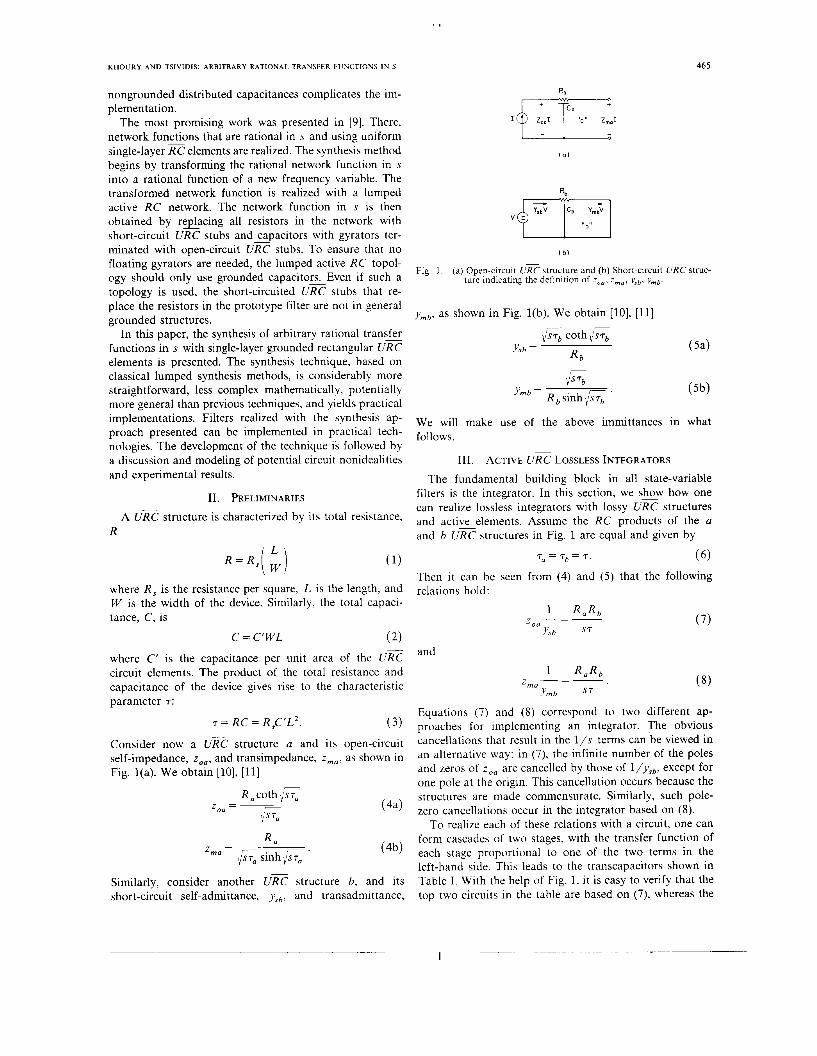
r = RC = R,C’L2. ( 3 ) Consider now a U= structure a and its open-circuit self-impedance, zoa, and transimpedance, zmu, as shown in Fig. l(a). We obtain [lo], [ll]
7 Racoth$sra ( 4 4 6, Zoa =
Similarly, consider another UR? structure h, and its short-circuit self-admittance, ysb, and transadmittance,
Rb
( b )
Fig. 1. (a) Open-circuit U= structure and (b) Short-circuit U= struc- ture indicating the definition of zoo* z,,, ysb, .ymb.
ymb, as shown in Fig. l(b). We obtain [lo], [ll]
We will make use of the above immittances in what follows.
111. ACTIVE U= LOSSLESS INTEGRATORS The fundamental building block in all state-variable
filters is the integrator. In this section, we show how one can realize lossless integrators with lossy URC structures and active elements. Assume the RC products of the a and h U= structures in Fig. 1 are equal and given by
ra = rb = r .
Then i t can be seen from (4) and (5) that the following relations hold:
( 6 )
(7)
and
(8) R a R b
- z m u - -
Y m b s r
Equations (7) and (8) correspond to two different ap- proaches for implementing an integrator. The obvious cancellations that result in the l /s terms can be viewed in an alternative way: in (7), the infinite number of the poles and zeros of zoa are cancelled by those of 1/ysb, except for one pole at the origin. This cancellation occurs because the structures are made commensurate. Similarly, such pole- zero cancellations occur in the integrator based on (8).
To realize each of these relations with a circuit, one can form cascades of two stages, with the transfer function of each stage proportional to one of the two terms in the left-hand side. This leads to the transcapacitors shown in Table I. With the help of Fig. 1, it is easy to verify that the top two circuits in the table are based on (7), whereas the

~
466
C
I F ROC, = RbCb =rl
V,='I sc, I
where
C m = G k
I f , fur ther ,
R, = R b = R , and thus C , = C b = C
C,; c GmR
TABLE I1 I h l I G R Z l O R >
~ --___
___- - CIRCUIT SCHEMATIC
L
I b
1 I where c. I R,r
Ro Rb
I f . fur ther .
bottom two are based on (8). All four circuits have the same transfer function, which is given in the right column along with a convenient symbol far later use. The parame- ter C,,, is the franscupacitunce of the circuits.
Any of the circuits in Table N can be used with an additional voltage-controlled current source (VCCS) to implement a voltage or current integrator. This is shown in Table 11, where we have switched from the VCCS symbol to the equivalent transconductor symbol. in anticipation of later usage in this paper.
The use of transconductance elements in the implemen- tation of the integrator is particularly well suited to MOS technology because MOS transistars can realize good transconductors [12], [13].
IV. EXTENSIONS OF THE T 'ECHNIQC~
In this section, we report some additional results. These appear less relevant than the elements discuv~ed abobe from a practical point of vie& at thir time. but are in- cluded for completeness.
4.1. Other Transcapacitors
By taking the inverse of both sides in each of (7) and (8). we obtain ysh( l /z, , ) = sr / ( R,R,) and ~ ~ , , , , , ( l / z n l a ) =
s r / ( R a R h ) . The circuits in Table I11 are easily seen to implement these two relations. C: is the transcapacitance of these circuits.
4.2. DIfferentiutors
Combining any of the circuits of Table 111 with a transresistor. one obtains the differentiators of Table IV. Depending on the order of cascading the transresistor and transcapacitor, the differentiator can process either voltage or current signals.
4.3. Inductors, Capucitors, and Resistors
Combining the C,,, and C: transcapacitor elements in Table I and I11 with controlled sources, one can obtain one-port inductors and capacitors as shown in Table V. The A, and A , networks in parts C and D of the table are the gains of voltage and current amplifiers. respectively. A resistor can be implemented with controlled sources, as shown in parts E and F of Table V.

KHOURY AND TSIVIDIS: ARBITRARY RATIONAL TRANSFER FUNCTIONS IN S 461
D
vn r G=G, E
R=R, F
I I I
v . REALIZATION OF GENERAL RATIONAL TRANSFER FUNCTIONS USING ACTIVE U= ELEMENTS
Since the fundamental two-terminal elements of Table V can be realized with active elements and U= structures it follows that in principle any RLC topology, passive or active, can be converted to an active U= topology using the elements developed here. While this result may be theoretically interesting, though, in practice state-variable structures using integrators (see Table 11) may be prefer- able.
As is well known, the state-variable simulation of a linear time-invariant system can be realized with integra- tors and weighted gain elements [14] and can implement any rational transfer function containing arbitrary poles and zeros. Examples of weighted summers are shown in Fig. 2. The weighted gain element in Fig. 2(a) is readily realized by paralleling transconductors. The output of this summer is a current. If a voltage output is desired, another transconductor, configured as a resistive load, can be used to convert the output current to a voltage, as shown in Fig. 2(b). Transresistance summers can also be implemented, and are the duals of Fig. 2(a) and (b). Fig. 2(c) shows an opamp-based weighted summer with voltage input and voltage output. The input-output formulations of the three weighted summers are readily derived and are given in the figure.
Implementing network transfer functions with integra- tors and weighted adders has several desirable properties in addition to being a popular lumped-circuit synthesis approach. One realization is the leapfrog topology [15]. The leapfrog topology simulates all the voltages and cur- rents in a passive LC ladder filter. Because LC ladders possess low passband sensitivity [2], [3], leapfrog filters retain such a characteristic. In addition, since filters that have low sensitivity to component tolerances typically
TI * T V i
v o = - 2 ( % ) V i I *,
( C )
Fig. 2. Various weighted summers for use in state-variable filter topolo- gies.
Fig. 3. A voltage integrator suitable for realization in MOS VLSI technologies
possess low noise, the leapfrog topology can yield lower noise than other topologies [16].
VI. EFFECT OF NONIDEALITIES ON PRACTICAL INTEGRATOR PERFORMANCE
Of all the possible integrator topologies that can be realized with the networks of Tables I and 11, the structure shown in Fig. 3 is particularly well suited to practical integrated implementations (as is the integrator formed by reversing the order of cascading) for several reasons. First, the integrator inputs and outputs are voltage signals for compatibility with other integrated circuit signal process- ing circuits. Second, MOS transistors can be used in VLSI (very large scale integration) to make good quality transconductors [12], [13]. Finally, the MOS transistor behaves as a U= structure for small signals when biased with zero drain-to-source voltage, as discussed in [19]. If techniques for nonlinearity cancellation and automatic tuning, known for lumped circuits [19], can be extended to

distributed implementations then the technique presented here can be used in a wide variety of filter architectures using MOS transistors as the oti!v circuit elements. Thus such filters could become possible in popular “digital” VLSI fabrication processes, in which capacitors are often not available. Previous work has shown that the realization of transistor-only filters in digital VLSI is feasible [17], [18], but those techniques use classical U c synthesis and cannot realize rational transfer functions based on lumped-network topologies as reported here.
The effect of several linear-circuit nonidealities on the performance of the lossless UF? integrator in Fig. 3 is analyzed here because the integrator is the fundamental building block for state-variable filters. Transconductor nonlinearity and the nonlinearity of Urn structures imple- mented with MOS transistors are not modeled in this paper, but they are important nonidealities that should be taken into account for specific designs. Nonidealities of the various differentiators, inductors. and capacitors pre- sented earlier are not modeled because they are unneces- sary for the state-variable realization of a linear system. The nonideal operation of the integrators using opamps is also not addressed: these integrators may be impractical since the U= element in the opamp’s feedback path can produce a large phase shift, resulting in instability [20], unless (difficult) frequency compensation techniques are applied.
First, the nonideality effect of noncommensurate U= structures in the integrator of Fig. 3 will be analyzed. We will show that the integrator can have phase lead or lag over a range of frequencies depending on whether T, or T~
is larger. The integrator will operate ideally if T, = T ~ . However. i f
the two U= structures are noncommensurate, nonperfect pole-zero cancellation occurs, resulting in degraded inte- grator operation. If the U= lines of stage U and stage h have RC products of ra and T ~ . respectively, then the integrator transfer function can be written as
E 105 - 6
l o 3
102
IO1
-10 ’
-IO2
- l o 3
- lo4
- l o 5
U
d
0.0 0.5 1.0 1.5 2 . J
( a )
w[
AT/T = -0.1
I 0.0 0.5 1 . 0 1 . 5 2 . 0
ox 1 h \ \ “ I
Fig. 4 Plot of the qualit! factor for the integrator - of Fig. 3 versus W T
for the c a ~ of 1ioncoiiirncn\iir;lte L’RC structures.
If 7, and T~ are mismatched as follows:
and
AT -~ T h ’ 7 - - (13) Gm,Gm, R a R coth \. sTa
s \ ‘ T ~ T ~ coth ST^ H , ( s ) = __ -- , (9) 2 _ _ _ _ _
then applying the definition of integrator quality factor to A convenient method of evaluating integrator performance is in terms of its equality factor, Q I ( w ) . The quality factor of an integrator is analogous to that of an inductor or capacitor and is a measure of the integrator’s phase error
following form:
(9). we obtain the following approximate expression. if the frequency of operation for the integrator is restricted to the range where W T < 1 :
3 [3]. If the integrator transfer function is placed in the Q f ( ( . ) = AT/.) ’ (14)
1
R ( w ) + j X ( w )
Clearly. the integrator quality factor can be positive or negative, corresponding to phase lead or phase lag. de- pending on the relative lengths of the N and h U= lines. The exact expression for Qr( w ) has been used to plot that quantity LnersuS in Fig, 4 for various values of AT/T.
Plotting Q r for positive values of AT/. in Fig. 4(a) shows that the integrator has phase lead while negative values of AT/T. shown in Fig. 4(b). produce phase lag. Notice that the magnitude of the integrator quality factor is high when W T is small. This occurs because at small W T . the fre-
H ( ‘a) = ___-___ I J ( I 0 )
where R ( u ) and x(0) are real and reactive terms, respec- tively, then the integrator quality factor is defined as [ 3 ]
( 11)
Ideally, the integrator has only ii reactive component. resulting in an infinite e,( w ) for all frequencies.
X ( w ) e,( W ) = R ( w )

KHOURY AND TSIVIDIS: ARBITRARY RATIONAI. TRANSFER FIJNCTIONS I N S 469
Fig. 5 . Schematic of the integrator of Fig. 3 with the resistive and capacitive loading of nonideal transconductors.
quency of operation is well below the poles and zeros of both U= structures (except for the desired pole at s = O), making the effect of the non-perfect pole-zero cancellation unimportant. However, as the frequency of operation rises, the pole-zero misalignment causes more severe perfor- mance degradation. The fact that an ideal integrator is approached as o r approaches zero, can also be appreci- ated by noting that in that case, structure a approaches a capacitor, and structure b a resistor, resulting in a G, - C integrator followed by a voltage gain element. Note that the desired pole at s = 0 is not affected by a r mismatch.
The quality factor of the integrator in Fig. 3 can also be degraded if the transconductors have nonidealities, as de- picted in Fig. 5. R,, and C,, model the total lumped resistance and capacitance at the output of transconductor Gml, while R,, and C,, model the corresponding quanti- ties at the output of transconductor Gm2. The resistance R , could be, for example, the output resistance of the transconductors. C,, and CL, can include lumped para- sitics associated with practical implementations of the U= elements.
The quality factor will first be evaluated for the special case that all operation is ideal except for transconductor finite output resistance. If R,, >> R a , R,, >> R , and or 61, Q,(o) can be approximated by
R L1
‘ a Q,( U ) = or--
The above result shows that the finite output resistance of the transconductors causes phase lead at low frequencies. This occurs because the finite output resistance at stage 1 prevents the integrator from having infinite gain at dc. Stage 2 has finite dc gain with or without nonideal circuit operation, so R ,, does not have a correspondingly decisive effect. This is why R,, dropped out in the approximation of (15).
Finally, the nonideal integrator in Fig. 5 is analyzed for the case of capacitive loading at the output of both transconductors; all other operation is assumed ideal. If C, >> CL1, C, >> C,, and or < 1, the approximate integra- tor quality factor is
‘a
The capacitive loading on the output of the two transcon- ductors causes the integrator to have phase lag that be- comes worse at higher frequencies.
( b )
Fig. 6. Reduced-circuit integrators. (a) Phase-lead integrator. (b) Phase- lag integrator.
The above results are equally valid for an integrator realized by interchanging the cascaded order of the two stages shown in Fig. 5.
Examining the expressions for the integrator quality factor in (14)-(16) we notice that to maximize the magni- tude of Q,, r should be made as small as possible for the cases of noncommensurate structures as well as capacitive loading. In contrast, r should be maximized to minimize the effect of resistive loading caused by transconductor inputs and outputs. These two requirements for r necessi- tate a compromise that can complicate the transconductor design. An alternative approach is to design the transcon- ductors, determine the capacitive and resistive loads that all U= structures see, and then purposely use structures that are noncommensurate with the proper value of Ar to provide the needed phase lead or lag to achieve an integra- tor with an infinite quality factor at its unity-gain fre- quency.
The circuit of Fig. 5 with both U= structures removed is practically the equivalent small-signal schematic or an uncompensatedtwo-stage opamp. By using the two com- mensurate URC structures as shown in the figure, the opamp can be compensated with a dominant pole without the use of a capacitor. We have already indicated that the lossless U= integrators developed permit the realization of analog filters in “digital” MOS processes and now we see that compensated opamps are also possible.
VII. REDUCED-CIRCUIT INTEGRATORS
The integrators presented so far implement in principle exactly the theoretical integrator transfer function. In t h s section we show two circuits that approximate the behav- ior of integrators for o r << 1.
The two “ reduced-circuit’’ integrators are depicted in Fig. 6. The performance of the circuits is characterized in terms of integrator quality factor. The integrator in Fig. 6(a) has a quality factor that is derived to be, for or <l:
The equation shows that the integrator quality factor is infinite at o = 0, but degrades as the frequency of opera-

470
0 -
-5 - m d -10 m E -15
-20
2 -25
-30
-35
D
D
z
r
tion is increased. Since Q I ( w ) is always positive, this integrator provides phase lead.
The quality factor of the integrator in Fig. 6(b) is derived to be, for O T < 1 :
~
~
-
-
-
-
~
-- 6 Q I ( W ) =---. (18)
LJ T
As in the previous example, the magnitude of the quality factor decreases with increasing 13 T : however, this integra- tor has phase lag as opposed to phase lead for O T < l . The integrator in Fig. 6(b) can be made to have the same quality factor magnitude as the one in Fig. 6(a) if its T is doubled in value, corresponding to an increase in the length of the U= structure by a factor of \iz (see (3)). The usefulness of having both a phase lead and a phase lag integrator with identical quality factor magnitudes is dis- cussed elsewhere [3], [20]; however. a simple explanation is warranted. Many filter structures, such as biquads, consist of a loop of integrators. If the sum of the integrator phase errors around the loop is zero, the biquad transfer function is nearly the same as would be obtained with ideal integra- tors. The phase lead and lag property of the reduced-cir- cuit integrators satisfy this property if the lengths of URC structures are designed appropriately.
Although the two integrators of Fig. 6 can be used with one another to obtain phase lead-lag cancellation in a biquad, such an effect can only kle achieved at frequencies below the first nonzero pole of both U= structures. This frequency range restriction suggests that filters realized with these integrators will need UR? lines with small RC products and consequently small L. To make the integra- tors less susceptible to lumped parasitic capacitances. the width of the U= structures, W. can be made large. However, depending on the physical structure of the U= element, the lumped parasitic capacitances can be propor- tional to W , restricting achievable performance. In the case of a U= structure implemented with an MOS transistor, both the drain and source junction capacitances as well as gate overlap capacitances are roughly proportional to W. Since the integrator of Fig. 3 can operate @ E r all frequen- cies, in theory, the capacitance of the URC line can be increased as much as needed to mask the effect of parasitic capacitances with increases in ,both L and W , without having to limit the freTency of operation below the first nonzero pole of the URC element. Although the nonideal- ity effects in practical implementations require further study, we believe the integrator of Fig. 3 (as well as the integrator obtained by reversing the cascading order of the two stages in Fig. 3) will in general be preferable to the reduced-circuit integrators of Fig. 6.
VIII. EXPERIMENTAL RESULTS To verify experimentally the concepts presented in this
paper, a second-order bandpass filter w a s implemented with commercially available transconductance amplifiers and large properly biased P-channel MOS transistors serv-
IraT& - -
Fig. 7. Schematic of the experimental bandpass U??? filter
5 1
-40 1 I 1 I I 1 1 1 1 1 ,
0 2.0 4.0 6.0 8.0 10
Mea.\ured magnitude rehponw o f the experimental filter with and M ithout tuning (solid c u n e s ) and simulated response (dotted curve).
FREQUENCY (kHz)
Fig. X.
ing as the L i z structures. The filter. shown in Fig. 7, is formed with a loop of two integrators consisting of the four U= elements and G,, through Gm4. Transconductor G,, sums the input signal and transconductor G,, damps the biquad. The integrators are realized with the structure of Fig. 3 and the weightedsummer of Fig. 2(a) is used for signal summation. The URC elements all had a nominal distributed resistance of 44.0 kQ and a capacitance of 1.5 nF. G,, through Gm4 are LM3080 transconductance am- plifiers biased for a nominal transconductance of 22 pA/V, while G,, and G,,, are biased for 3.2 pA/V. Since the LM3080 transconductors require input bias current, LF347 opamps connected in &e voltage follower mode were inserted between the URC structures and transconductor inputs to minimize loading. In an integrated MOS design, such buffering would be unnecessary.
The measured frequency response of the filter is shown with the solid-curves in Fig. 8 with and without manual tuning. The manual tuning, accomplished by varying the gate voltage on all four URC elements simultaneously, shows what the outcome of an automatic on-chip tuning mechanism would be in an integrated solution. Based on a purely ideal analysis of this filter one would expect a
__* -

KHOURY AND TSIVIDIS: ARBITRARY RATIONAL TRANSFER FUNCTIONS IN S 471
center frequency of 2260 Hz and a passband gain of 0 dB. Several parasitic effects in this discrete realization cause the response to differ from ideality. First, the transconduc- tors and voltage follower opamps have nondominant poles causing the integrators to have excess phase sluft at the center frequency, that in turn causes the maximum gain to exceed 0 dB. Gain peaking is enhanced further by the parasitic capacitances at the output of each transconduc- tor. Second, the center frequency is not ideal due to mismatches in the transistors and among the transconduc- tors. The filter was simulated with the ADVICE circuit analysis program [21] with as many of the nonideal effects accounted for as possible. The simulation result is shown with the dotted curve in Fig. 8 and agrees well with the measurement after tuning was performed. Although the nonidealities have not been perfectly modeled, feasibility of the technique has been demonstrated.
In practice, one would build this type of U= filter on a clup where the transconductors and parasitics could be well modeled and where tight matclung of components is possible. Additionally, on-chip tuning circuits would be used to control both the center frequency and Q of the bandpass filter to achieve a precise response.
There are two major tasks for malung the U= ap- proach viable in MOS technology: i) transconductor de- sign and ii) nonlinearity cancellation. The transconductor requires an extremely high bandwidth and output impedance so the integrator in Fig. 3 can achieve a high quality factor. Note that the transconductor requirements can be eased if noncommensurate U= structuresare used as suggested in Section VI. (Noncommensurate URC struc- tures can be realized with identical MOS transistors having different bias voltages on their gates. In fact, the difference in the gate voltages can be controlled with an on-clup tuning system for adjusting the quality factors of the integrators.) Canceling the nonlinearity of the MOS U= elements is essential to achieve good dynamic range. Use of fully balanced structures will improve the linearity to a first order, but it would be preferable if better nonlinearity cancellation schemes could be developed.
IX. CONCLUSION
This paper has presented a new network synthesis tech- nique that relies solely on grounded single-layer U= lines and active elements to realize linear time-invariant systems having transfer functions that are rational in s. In contrast to earlier distributed network research, the method developed synthesizes networks directly in the s plane, uses classical approximation theory already developed for lumped networks, and requires only grounded single-layer rectangular U= structures. The technique shows that distributed networks can be synthesized in a straightfor- ward manner while possessing useful network functions, in contrast to long-held beliefs. In addition, the realization technique is applicable to tlun-film hybrid circuits and may permit the monolithic integration of mixed analog-
digital circuits in “digital” MOS processes in which capaci- tors are not available, if a way is found for nonlinearity cancellation.
ACKNOWLEDGMENT
The authors thank Dr. B. B. Bhattacharyya, Dr. M. S. Ghausi, Dr. R. Schaummann, Dr. M. N. S. Swamy, Dr. R. W. Wyndrum, Jr. and several unknown reviewers
their comments on the paper.
REFERENCES R. W. Wyndrum. Jr., “The realization of monomorphic thin film distributed RC networks,” in IEEE Convention Rec., vol. 13, part
G. Temes and J. LaPatra, Introduction to Circuit Synthesis and Design. New York: McGraw-Hill, 1977. A. Sedra and P. Brackett. Filter Theoy und Design: Active and Pussire, Beaverton, OR, Matrix, 1978. R. O’Shea “Synthesis of driving point and transfer functions using distributed RC networks,” IEEE Truns. Circuit Theory, vol. CT-12, pp. 546-554, Dec. 1965. K. Heizer, “Distributed RC networks with rational transfer func- tions,” IRE Truns. Circuit Theory, vol. CT-9, pp. 356-362, Dec. 1962. R. Schaummann. “On the realization of arbitrary voltage transfer functions with active lumped distributed networks,” A E l / , vol. 27, pp. 139-144, Mar. 1973. Y. Fu and J. Fu, “Synthesis of active distributed RC networks,” IEEE Truns. Circuit Theory, vol. CT-13, pp. 259-264, Sept. 1966. B. Psenicka, J. Pomichalek, and K. Stepanek, “Distributed RC active networks with rational transfer functions,” in Proc. Int. Synip. on Circuits und Systems. pp. 228-231, 1976. M. S. Abougabal, B. B. Bhattacharyya, and M. N. S. Swamy, “A low sensitivity active distributed realization of rational transfer functions,” IEEE Truns. Circuits S.pst., vol. CAS-21, pp. 391-395, May 1974. M. Ghausi and J. Kelly. Introduction to Distributed-Parameter Netnorhs. W. Heinlein and W. Holmes, Actiue Filters for Integrured Circuits: Fundumentuls und Desigr7 Methods. New York, Springer-Verlag, 1974. Y. Tsividis. Z. Czarnul, and S. C. Fang, “MOS transconductors and integrators with high linearity,” Electron. Lett., vol. 22, Feb. 1987. F. Krummenacher and N. Joehl, “A 4-MHz CMOS continuous-time filter with on-chip automatic tuning,” IEEE J . Solid-Stute Circuits, vol. 23. pp. 750-758, June 1988. C.-T. Chen. Inrroduction to Lineur System Theorp. New York: Holt. Rinehart, and Winston, 1970. 0. Wing, “Ladder network analysis by signal flow graph applica- tion to analog computer programming,” IRE Truns. Circuit Theoy, vol. CT-3. pp. 289-294. Dec. 1956. W. Snelgrove and A. Sedra, “Synthesis and analysis of state-space active filters using intermediate transfer functions,” IEEE Truns. Circuits Syst.. vol. CAS-33, pp. 287-301, M a r 1986. Y. Tsividis, “Minimal transistor-only micropower integrated VHF active filter.” Electron. Lett., vol. 23, pp. 777-778. July 1987. L. J. Pu and Y. Tsividis. “Transistor-only frequency-selective cir- cuits.” in Proc. 1988 IEEE I n t . Synip. on Circuits und S.vstems, pp. 2851-2854, May 1988. Y. Tsividis, M. Banu. and J. Khoury. “Continuous-time MOSFET-C filters in VLSI,” IEEE Truns. Circuits Syst., vol. CAS-33, pp. 125-140, Feb. 1986. J. Khoury, “Realization of lumped and distributed integrated con- tinuous-time filters,” Ph.D. dissertation, Columbia Univ., New York, 1988. L. Nagel, “ADVICE for circuit simulation,” in Proc. I n t . Symp. on Circuits und Systems. Houston, TX, Apr. 1980.
10, pp. 90-95, 1965.
New York: Holt, Rinehardt, and Winston, 1968.
John M. Khoury (M’85) received the B.S. degree from Columbia Univer- sity in 1979, the S.M. degree from the Massachusetts Institute of Tech-

472
nology in 1980 and the D.Eng. Sc. degree In 1988 from Columbia University. all in electrical engi- neering.
He joined ATBrT Bell Laboratories in 1979 and has been a Member of the Technical Staff in the Analog MOS Subsystems Department at the Murray Hill location since 1984. He designs ana- log CMOS circuits for telecommunications appli- cations and is interested in circuit design and signal processing,. He has also been an adjunct professor in the Department of Electrical Engi-
neering at Columbia University. Dr. Khoury is a co-recipient of the 1987 Darlington Award.
11 51 I R I N S A C rIONb ON ClKCUITb AND SYSTEMS, VOL 37, NO 4, APRIL 1990
Yannis P. Tsividis (S’71-M’74-SM’8l-F’86) re- ceived the Ph.D. degree from the University of California, Berkeley, in 1976.
He is currently a Professor at Columbia Uni- versity, New York, and is the author of Operu- tion und Modeling of the MOS Trunsistor (McGraw-Hill, 1987) and co-editor and co-author of Design of MOS VLSI Circuits for Telecomniu- nicutions (Prentice-Hall, 1985).
Dr. Tsividis has been a member of the Admin- istrative Committee of the IEEE Circuits and
Systems Society and of the United Nations Advisory Committee on Science and Technology for Development. He is the recipient of the 1984 IEEE W. R. G. Baker Best Paper Award and the 1986 European Solid-State Circuits Conference Best Paper Award, and co-recipient of the 1987 IEEE Circuits and Systems Society Darlington Best Paper Award.
- -


![Modeling optical surfaces by Non-Uniform Rational B ... · Non-Uniform Rational B-Splines (NURBS)[1] Davide Bianchi, Claudio Ferrero and Manuel Sánchez del Río* ESRF European Synchrotron](https://img.pdfslide.net/doc/110x75/5f4f0eee07e7574b3d12234f/modeling-optical-surfaces-by-non-uniform-rational-b-non-uniform-rational-b-splines.jpg)