Embed Size (px)
Citation preview
SYNTHESIS TECHNIQUESFOR
BUILT-IN SELF-TESTABLE DESIGNS
LaNae Joy Avra
CRC Technical Report No. 94-6(CSL TR 94-633)
July 1994
CENTER FOR RELIABLE COMPUTINGComputer Systems Laboratory
Departments of Electrical Engineering and Computer ScienceStanford University
Stanford, CA 94305-4055
Copyright 1994 by LaNae Joy AvraAll Rights Reserved
SYNTHESIS TECHNIQUESFOR
BUILT-IN SELF-TESTABLE DESIGNS
A DISSERTATION
SUBMITTED TO THE DEPARTMENT OF ELECTRICAL ENGINEERING
AND THE COMMITTEE ON GRADUATE STUDIES
OF STANFORD UNIVERSITY
IN PARTIAL FULFILLMENT OF THE REQUIREMENTS
FOR THE DEGREE OF
DOCTOR OF PHILOSOPHY
LaNae Joy Avra
June 1994
i
ABSTRACT
Hardware synthesis techniques automatically generate a structural hardware implementation
given an abstract description of the behavior of the design. Many different hardware designs can
implement a given behavioral description, a subset of which also meet specified requirements
such as cost, performance, and testability. Existing synthesis techniques typically use minimum
cost or maximum performance as the primary criteria for selecting the best hardware
implementation. This dissertation describes new synthesis techniques whose primary objective
is to satisfy requirements associated with a specific built-in self-test (BIST) architecture.
The use of BIST techniques (design techniques that allow a circuit to test itself) has long
been recognized as a means to reduce system life cycle test and maintenance costs. BIST
provides shorter test times and allows the use of low-cost test equipment during all stages of the
product life: production test, acceptance test, field maintenance, and failure diagnosis. However,
hardware overhead, performance degradation, and increased design time are often cited as
reasons for the limited use of BIST. When BIST techniques are used, they are often added after
the system logic has been designed. At this point, system logic features that may increase BIST
overhead or reduce the effectiveness of the BIST operation are expensive to change.
This dissertation describes new synthesis techniques that address two of the major issues
associated with BIST: 1) implementation costs due to increased design time, area overhead,
increased power consumprtion, and performance degradation and 2) test effectiveness due to
system logic design decisions. Our synthesis procedures use criteria associated with the
specified BIST architecture to guide the generation of the system logic, allowing for design
decisions that reduce BIST overhead and improve BIST effectiveness. In particular, the primary
objective of our synthesis techniques is to generate low-cost, built-in self-testable designs that are
free of the types of system bistable dependencies that can reduce the effectiveness of the
embedded, multiple input signature registers (MISRs) that are used to perform BIST operations.
One type of system bistable dependency that can be a problem for BIST occurs in a self-
adjacent register, where the register inputs are a function of its outputs. To address this problem,
we have developed a high-level synthesis technique that minimizes the number of self-adjacent
registers in the generated design without increasing the latency of the design. Some system
bistable dependencies provide opportunities for sharing BIST and scan logic with system logic,
reducing the area and improving the performance of the design. We show that introducing
certain, beneficial types of scan dependence in the design can increase logic sharing
opportunities and can improve BIST effectiveness. Other BIST design techniques attempt to
avoid all types of scan dependence. We have developed a logic synthesis technique that analyzes
the system bistable dependencies, then arranges the bistables in the MISR to maximize beneficial
ii
scan dependence. For data path logic, we have developed a new scan path architecture, called
orthogonal scan path, for which the shift direction is orthogonal to the shift direction in
traditional scan paths. We show that using an orthogonal scan path increases the number of
beneficial scan dependencies between data path logic bistables. We have implemented our
synthesis-for-BIST techniques in a computer-aided design system, which serves as a platform for
experimentation with existing and future synthesis-for-test techniques.

iii
ACKNOWLEDGMENTS
I express my deepest appreciation to my adviser, Edward J. McCluskey, for his guidance,
support, and instruction during my time at Stanford. His suggestions have greatly enhanced both
the technical content and the presentation of this dissertation, and his enthusiasm for learning and
for teaching have been a constant source of inspiration.
I am most grateful to my colleagues at the Center for Reliable Computing who have provided
many hours of discussions, manuscript editing, and companionship: Piero Franco, Hong Hao,
Siyad Ma, Samy Makar, Samiha Mourad, Rob Norwood, Nirmal Saxena, Alice Tokarnia, and
Nur Touba. I especially wish to thank the CRC visitors who have worked so diligently on the
Odin software: Jean-Charles Giomi, Francoise Martinolle, Laurent Gerbaux, Dave Brokaw, and
Gian Luigi Sartori. Their contributions have greatly improved the quality and usefulness of the
tool. Many thanks, also, to Siegrid Munda for her expert administrative support.
I would like to thank my associate adviser, Giovanni De Micheli, for his useful comments
and suggestions for developing the high-level synthesis algorithms. Thanks, also, to the
members of his group that provided support and technical advice: David Ku, Michiel Ligthart,
Polly Siegel, and Jerry Yang.
I greatly appreciate the industry feedback and software donations provided by Dave Coelho
and Rick Lazansky of Vantage Analysis Systems, Inc., and Jacob El Ziq of Compass Design
Automation.
Finally, I wish to thank my family. I thank my husband, Rick, for his support,
encouragement, and technical advice. His expertise in the design, validation, testing, and
manufacturing of VLSI chips provided invaluable real-world perspective to the material in this
dissertation. I am grateful to both Rick and my daughter, Tamsin, for their patience,
understanding, and unconditional love, without which this work would not have been possible.
Thanks, also, to my parents for instilling in me the self-confidence necessary to pursue my goals
and for providing me with every opportunity to learn.
This work was supported in part by Digital Equipment Corporation, Low-End Diagnostics
Group, and in part by the Innovative Science and Technology Office of the Strategic Defense
Initiative Organization and administered through the Office of Naval Research under Contract
Nos. N00014-85-K-0600 and N00014-92-J-1782, and in part by the National Science Foundation
under grant Nos. MIP-8709128 and MIP-9107760.
iv
TABLE OF CONTENTS
Abstract ................................................................................................................................ i
Acknowledgments.............................................................................................................. iii
List of Tables ..................................................................................................................... vi
List of Illustrations ............................................................................................................ vii
1 Introduction................................................................................................................ 1
1.1 Motivation ............................................................................................................ 1
1.2 Contributions........................................................................................................ 3
1.3 Outline.................................................................................................................. 4
2 Embedded BIST Architectures ............................................................................. 5
2.1 Parallel BIST Architecture ................................................................................... 6
2.2 Circular BIST Architecture ................................................................................ 12
2.3 Reconfigurable Register Design ........................................................................ 13
3 Allocation and Binding for Parallel BIST........................................................ 16
3.1 High-Level Synthesis Tasks............................................................................... 17
3.2 Register Conflict Graph ..................................................................................... 18
3.3 Implementation and Results ............................................................................... 20
3.4 Contributions...................................................................................................... 22
4 Synthesis for Scan Dependence.......................................................................... 24
4.1 Scan Dependence ............................................................................................... 25
4.2 Synthesis for Scan Dependence ......................................................................... 28
4.3 Implementation and Results ............................................................................... 30
4.3.1 Area and Delay Results .......................................................................... 31
4.3.2 Fault Simulation Results ........................................................................ 34
4.4 Contributions...................................................................................................... 35
5 Scan Dependence in Data Path Logic ............................................................... 36
5.1 Orthogonal Scan Path Architecture.................................................................... 37
5.2 Scan Dependence Functions in Data Path Logic ............................................... 37
5.3 Results ................................................................................................................ 39
5.4 Contributions...................................................................................................... 40
6 Synthesis-for-Test Design System ..................................................................... 41
v
6.1 Overview ............................................................................................................ 41
6.2 Design System Input and Output ....................................................................... 42
6.2.1 VHDL Descriptions ............................................................................... 43
6.2.2 Component Library ................................................................................ 44
6.3 Data and Control Flow Graphs .......................................................................... 44
6.4 High-Level Synthesis Techniques ..................................................................... 47
7 Concluding Remarks ............................................................................................. 50
References ......................................................................................................................... 52
vi
LIST OF TABLES
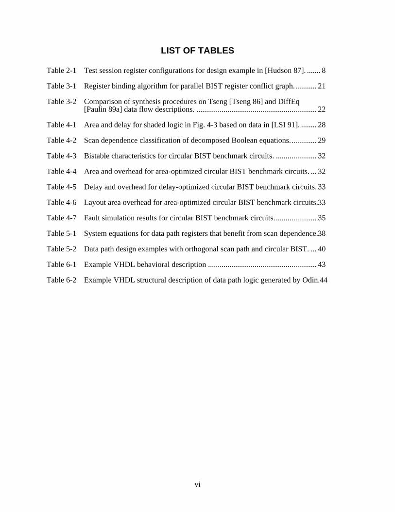
Table 2-1 Test session register configurations for design example in [Hudson 87]. ....... 8
Table 3-1 Register binding algorithm for parallel BIST register conflict graph............ 21
Table 3-2 Comparison of synthesis procedures on Tseng [Tseng 86] and DiffEq[Paulin 89a] data flow descriptions. .............................................................. 22
Table 4-1 Area and delay for shaded logic in Fig. 4-3 based on data in [LSI 91]. ........ 28
Table 4-2 Scan dependence classification of decomposed Boolean equations.............. 29
Table 4-3 Bistable characteristics for circular BIST benchmark circuits. ..................... 32
Table 4-4 Area and overhead for area-optimized circular BIST benchmark circuits. ... 32
Table 4-5 Delay and overhead for delay-optimized circular BIST benchmark circuits. 33
Table 4-6 Layout area overhead for area-optimized circular BIST benchmark circuits. 33
Table 4-7 Fault simulation results for circular BIST benchmark circuits. ..................... 35
Table 5-1 System equations for data path registers that benefit from scan dependence. 38
Table 5-2 Data path design examples with orthogonal scan path and circular BIST. ... 40
Table 6-1 Example VHDL behavioral description ........................................................ 43
Table 6-2 Example VHDL structural description of data path logic generated by Odin. 44
vii
LIST OF ILLUSTRATIONS
Figure 1-1 Test scenario for life cycle of integrated circuit part. ...................................... 1
Figure 1-2 Built-in self-test configuration......................................................................... 2
Figure 2-1 Parallel BIST architecture................................................................................ 7
Figure 2-2 Self-adjacent register implemented with CBILBO ........................................... 9
Figure 2-3 LFSR and MISR configurations for Fig. 2-1 ................................................. 11
Figure 2-4 Circular BIST architecture............................................................................. 13
Figure 2-5 Reconfigurable register.................................................................................. 14
Figure 2-6 MISR error capture capabilities ..................................................................... 15
Figure 3-1 High-level synthesis example ........................................................................ 17
Figure 3-2 Register conflict graph example .................................................................... 19
Figure 3-3 Testability conflict edges ............................................................................... 20
Figure 4-1 Embedded MISR with scan dependence ....................................................... 25
Figure 4-2 Fault simulation results of BIST operation of circular BIST circuits withmaximum scan dependence. .......................................................................... 26
Figure 4-3 Scan dependence solutions for Z2 = Q1 + f .................................................. 28
Figure 4-4 Beneficial scan dependence implementations ............................................... 29
Figure 5-1 Orthogonal scan path example....................................................................... 37
Figure 5-2 Live variable motion ...................................................................................... 40
Figure 6-1 Odin design system overview. ....................................................................... 42
Figure 6-2 DCFG example .............................................................................................. 45
Figure 6-3 Data flow graphs ............................................................................................ 46
Figure 6-4 High-level synthesis example ........................................................................ 48
Figure 6-5 Control logic state machine description for Fig. 6-2. .................................... 49


1
1 INTRODUCTION
1.1 MOTIVATION
An integrated circuit part such as a chip, multi-chip module, board, or system must be
thoroughly tested in order to determine whether or not it is defective. Different types of tests are
applied to the part at various times in its life cycle to detect different types of failures. For
example, the part manufacturer applies production tests to the part to determine whether or not
there are manufacturing defects, whereas the end user applies field tests to identify failures
caused by stressful conditions in the operating environment (e.g., radiation, vibration) or
reliability problems within the part (e.g., electromigration). Figure 1-1 illustrates a possible test
scenario that encompasses the entire life cycle of an integrated circuit part. In the first phase of
testing, the manufacturer applies production tests in order to prevent parts with manufacturing
defects from being shipped to the customer. Next, the customer applies acceptance tests to
determine whether or not the parts should be placed in field operation. Acceptance tests identify
parts that have been damaged during shipping, or parts that don’t meet customer specifications.
Parts that pass acceptance testing are then assembled into systems and placed into field
operation. Field tests are applied to a system that has failed in the field in order to identify the
defective component parts that must be replaced. For each testing phase in this particular
scenario, diagnostic tests are applied to rejected parts to determine the cause of failure in an
effort to improve the manufacturing process.
ProductionTest
DiagnosticTest
ShippedParts
End UserParts
Rejected Parts
TestProduced
PartsGoodBad
Pass
FailAcceptance
TestFieldTest
Good
Bad
ManufacturingProcess
Figure 1-1 Test scenario for life cycle of integrated circuit part.
The goal in any test scenario is to apply the most rigorous tests possible, tests for which the
number of good parts that fail, but most importantly, the number of bad parts that pass (called
test escapes) are minimized. The quality of a test is a function of how many of the targeted
failures are detected by the test, how well the targeted failures represent actual defects, and how
easily the part can be tested. As integrated circuit parts become more and more complex, dense,
and inaccessible, rigorous testing becomes less feasible unless design practices are used that
allow for easier testing. These design practices, called design-for-testability (DFT) techniques,
simplify the test development task by constraining the design to easy-to-test structures, thereby
making it easier to generate and apply tests that detect all of the targeted failures. However,

2
rigorous testing can still be impractical due to the expensive external test equipment required to
apply the tests.
Built-in self-test (BIST) is a DFT technique that allows a part to test itself. BIST techniques
such as those described in [McCluskey 85], [McCluskey 86], [Bardell 87], and [Abramovici 90]
have long been recognized as a means to reduce life cycle test and maintenance costs by
embedding external tester features, such as test pattern generation (TPG) and output response
analysis (ORA), into the part that contains the circuit under test (CUT) (Fig. 1-2). BIST can
provide shorter test times than externally-applied tests and allows the use of low-cost test
equipment during all stages of the product life including system debug, production test, field
maintenance, and failure diagnosis. Even though industry use of BIST techniques is becoming
more common [Gelsinger 86], [Lake 86], [Nozuyama 88], [Ratiu 90], [Starke 90], [Bardell 91],
[Illman 91], [Preissner 92], [Sinaki 92], [Yokomizo 92], [Bonnenberg 93], [Broseghini 93],
[Gage 93], [Langford 93], [Patel 93], area overhead, performance degradation, and increased
design time are often cited as reasons for the limited use of BIST.
CircuitUnderTest
(CUT)
Good/BadTestMode
Integrated Circuit Part
TestPatternGenerator
OutputResponseAnalyzer
ORA
TPG
Figure 1-2 Built-in self-test configuration.
Traditional design methods separate the tasks of system logic design (design of the logic that
implements the normal operation of the part) and BIST logic design. During the initial stages of
design, system logic issues take priority over BIST issues such as selection of the most
appropriate BIST technique for the system logic, BIST logic implementation, and evaluation of
the BIST operation. As the design progresses, time-to-market pressures often cause the
postponement of BIST design until the end of the design process at which point little time is
available to address BIST issues, and any mistakes made are expensive to fix. Automated BIST
synthesis techniques, where BIST logic is added or a BIST architecture is selected after the
system logic has been designed [Abadir 85], [Zhu 88], are valuable in that they reduce the design
time and the number of design mistakes by automating the BIST logic design process.
Unfortunately, earlier system logic design decisions can reduce the effectiveness and increase the
overhead of the implemented BIST technique.
Hardware synthesis techniques automatically generate a structural hardware implementation
given an abstract description of the behavior of the part. Many different hardware designs can
implement a given behavioral description, a subset of which also meet specified requirements
such as cost, performance, and testability. Current research in hardware synthesis techniques

3
(e.g., [Brayton 87], [McFarland 88], [De Micheli 94]) typically focuses on the use of minimum
area or maximum performance as the primary criteria for selecting the best hardware
implementation. Some synthesis-for-testability techniques attempt to generate the lowest-cost,
highest-performance implementation that also meets certain specified testability requirements
such as irredundant combinational logic [Hachtel 89], [Bryan 89] or robustly delay-fault testable
logic [Devadas 90], [Jha 92]. Testable logic is a necessary, but not sufficient, condition for high-
quality BIST operation. This dissertation describes new synthesis-for-BIST techniques that have
the primary objective of satisfying requirements associated with a specific BIST architecture
when generating the system logic structural implementation. Cost is minimized and performance
is maximized to the extent that BIST requirements are not compromised. These new synthesis
techniques address two of the major issues associated with generating self-testable designs: 1)
increased implementation costs due to added design time, area overhead, and performance
degradation, and 2) reduced self-test effectiveness due to system logic design decisions.
Considering BIST issues during system logic synthesis allows for the generation of system logic
that is optimized for a particular BIST architecture and that can be more effectively tested by the
BIST operation.
1.2 CONTRIBUTIONS
This dissertation describes new synthesis techniques that use the requirements of the
implemented BIST architecture to guide the synthesis of the system logic in order to improve the
effectiveness of the self-test operation and to reduce the BIST logic overhead. In developing
these new techniques, we have focused on embedded BIST architectures because they provide
opportunities for the sharing of system and test logic. Logic sharing makes it possible to reduce
the area overhead of the BIST logic and improve the performance of the generated design. In
particular, the following are the contributions of this dissertation:
• We have developed and implemented a new register allocation and binding algorithm for
high-level synthesis that generates designs with a minimum number of self-adjacent registers
[Avra 91]. This technique is used for parallel BIST architectures.
• We have formalized the concept of scan dependence in embedded BIST architectures and have
presented fault simulation data showing that, if ignored, scan dependence can significantly
reduce the effectiveness of the BIST operation [Avra 94a].
• We have identified certain types of scan dependence that can be beneficial to the design and
have developed new output response analysis (ORA) structures that take advantage of them
[Avra 93], [Avra 94a].
• We have developed and implemented a new synthesis for scan dependence technique that
maximizes the amount of beneficial scan dependence in the design [Avra 93], [Avra 94a].

4
• We have developed a new scan path architecture that increases the amount of beneficial scan
dependence in data path logic [Avra 92].
• We have implemented a synthesis-for-test computer-aided design tool that includes the
synthesis techniques described in this dissertation and generates a self-testable design given a
behavioral VHDL description of the design [Avra 90], [Avra 94b].
1.3 OUTLINE
This dissertation is organized as follows. In Sec. 2, we describe in detail the operation and
implementation of two embedded BIST architectures: parallel BIST and circular BIST. Parallel
BIST is the target BIST architecture of the synthesis technique described in Sec. 3, and circular
BIST is the target architecture of the synthesis techniques described in Secs. 4 and 5. We also
describe a register design that can be used in the parallel and circular BIST architectures. We use
this register design to illustrate the BIST concepts and design techniques presented in the
remainder of the dissertation. In general, each section discussing the contributions of this
dissertation (Secs. 3-6) is a summary of material previously published by the author and included
in Appendices I-IV. Section 3 contains a description of a high-level synthesis technique that
generates the system logic for a parallel BIST architecture. In Sec. 4, we define scan dependence
and illustrate its advantages and disadvantages with a simple example. We then describe a
synthesis technique that arranges the system bistables into MISRs such that beneficial scan
dependence is maximized. We illustrate the technique using the circular BIST architecture. In
Sec. 5, we show that beneficial scan dependence can be increased in data path logic when an
orthogonal scan path configuration is used. Section 6 is an overview of the synthesis-for-test
computer-aided design tool the implements the described synthesis techniques. The tool is
intended to be a platform for experimentation with existing and future test synthesis and
synthesis-for-test techniques. Section 7 concludes this dissertation.
5
2 EMBEDDED BIST ARCHITECTURES
BIST techniques are implemented by including a test pattern generator (TPG) and output
response analyzer (ORA) in the part (e.g., chip, multi-chip module, board) that contains the
circuit under test (CUT). During BIST operation, the TPG applies test patterns to the inputs of
the CUT and the ORA captures the response of the CUT to those test patterns. Typically, the
TPG and ORA are implemented such that they automatically generate patterns and analyze
responses at test time so that the test pattern and test response storage requirements are
minimized. Embedded BIST architectures use reconfigurable system bistables to implement
both the normal system operation and the BIST TPG and ORA operations. Since the BIST logic
is combined with the system logic, opportunities exist for synthesis technique to generate
hardware that can be shared by both the system and test operations, resulting in improved
performance and reduced cost. However, in addition to system logic issues such as performance
and cost, the synthesis technique must be capable of addressing issues that affect the quality of
the BIST operation, issues such as self-test time, and TPG and ORA effectiveness. We discuss
these issues in this section.
Most BIST architectures use pseudo-random pattern generators such as linear feedback shift
registers (LFSRs) or weighted random pattern generators [Waicukauski 89] to perform TPG
operations. The TPGs are called pseudo-random because, while they generate patterns with
characteristics that are similar to randomly-generated patterns, their behavior is deterministic.
The test is therefore repeatable, and the results of the test can be compared with expected results.
In order to test for all possible combinational faults (e.g., single and multiple stuck-at faults)
within an n-input cone of combinational logic in the CUT, where a cone of logic is delimited by
starting at a combinational logic output (either a primary output or a bistable input) and tracing
backwards through the gates to each input (either a primary input or a bistable output), a TPG
must be capable of applying all 2n possible test patterns. To test for pattern-dependent faults
[Hao 91], delay faults, or faults that cause combinational logic to behave sequentially, the TPG
may be required to generate multiple sequences of the 2n possible patterns. Faults that affect
more than one cone of logic (e.g., a bridging fault between the inputs of two logic gates that are
in different cones) can be detected if a single TPG covers multiple cones. We evaluate the TPGs
generated by our synthesis techniques in terms of their ability to generate 2n different test
patterns for each n-input cone of logic. Even though it may be determined that not all of the 2n
test patterns need to be applied during BIST operation, it is difficult to determine a priori which
subset of test patterns will be required to provide a high fault coverage test for each CUT.
Therefore, the TPGs must be designed such that they could generate all 2n different test patterns
if necessary. This is known as the “philosophy of possible exhaustion” [Bardell 87]. Also, if all

6
2n test patterns can be generated, one can use probabilistic models, based on the number of test
patterns applied and the detectabilities of the faults in the CUT, to estimate the fault coverage
provided by the TPG [McCluskey 88], thus avoiding expensive and time-consuming fault
simulations.
An ideal ORA is capable of analyzing the response of each test pattern applied to the CUT.
In practice, of course, this is not feasible for a built-in ORA. Instead, most BIST architectures
use ORAs, such as multiple-input signature registers (MISRs), that compact the test response,
resulting in a loss of information. Thus, under certain error conditions, the test response of a
faulty CUT may be indistinguishable from the test response of a fault-free CUT, a phenomenon
known as aliasing. Our synthesis techniques assume that MISRs are used as the ORAs in the
implemented BIST architecture and attempt to minimize the amount of aliasing in those MISRs.
In this section, we describe two embedded BIST architectures, parallel BIST and circular
BIST, and discuss BIST-related synthesis issues for each. In Sec. 2.1, we describe parallel BIST,
emphasizing often-overlooked implementation complexities that must be addressed by the
synthesis technique so that it generates a design that performs a high-quality BIST operation.
The synthesis technique described in Sec. 3 generates designs with parallel BIST architectures.
The synthesis techniques described in Secs. 4 and 5, though applicable to all BIST architectures
that use embedded MISRs, generate designs that use the circular BIST technique. We describe
the assumed circular BIST architecture in Sec. 2.2. In Sec. 2.3, we describe one possible
implementation of a reconfigurable register design for embedded BIST architectures. The
register is configured as a normal parallel load register for system operation. During BIST
operation, it is configured as either a maximum-length LFSR for test pattern generation or as a
MISR for output response analysis.
2.1 PARALLEL BIST ARCHITECTURE
The parallel BIST architecture [Konemann 80] is an embedded BIST architecture in which
system registers are reconfigured to perform either LFSR or MISR operations during BIST. The
built-in logic block observer (BILBO) register [Konemann 79] is often used to implement the
system registers in parallel BIST architectures. A possible implementation of the BILBO register
is described in detail in Sec. 2.3. Variations of the parallel BIST architecture are discussed in
[McCluskey 81], [Krasniewski 85], [Hudson 87].
Figure 2-1 illustrates how the parallel BIST architecture is used to test a block of data path
logic that consists of five registers (R1-R5), five combinational logic units (CLU1-CLU5),
primary input signals (PI), and primary output signals (PO). During normal operation (Fig. 2-
1a), the system registers are configured to load data from the outputs of the CLUs. Prior to
performing BIST operation, the system bistables must begin in a known state. This can be

7
accomplished by configuring the registers into a scan path and shifting in known data or by
configuring the registers to perform a reset operation. During BIST operation, the registers are
configured as either LFSRs or MISRs. At each clock cycle, pseudo-random test patterns are
applied to the inputs of the CLUs by the LFSRs at the same time that the test results (the outputs
of the CLUs) are compacted in the MISRs. Figures 2-1b and 2-1c represent two different test
sessions of the BIST operation, where each test session consists of a unique mapping of registers
to LFSRs and MISRs. CLU3, CLU4, and CLU5 are tested during the first test session (Fig. 2-
1b), and CLU1 and CLU2 are tested during the second test session (Fig. 2-1c). After each test
session, the registers are configured into a serial shift path so that the test results can be shifted
out and compared with expected results. This comparison can be performed either by external
test equipment or by BIST control logic that may be included as part of a test access port
controller [IEEE 90]. The BIST control logic also generates signals that control the
configuration of the system registers.
R1
R3
CLU3
PI PI R2
CLU4 CLU5
PI
R4 R5
CLU2
PI PIPO
CLU1
CLU3
PI PI
CLU4 CLU5
PI
CLU2
PI PIPO
CLU1
CLU3
PI PI
CLU4 CLU5
PI
CLU2
PI PIPO
CLU1
LFSR
MISR MISR MISR
MISR
LFSR
MISR
LFSR LFSR
LFSR
(a) (b) (c)
Figure 2-1 Parallel BIST architecture: (a) normal operation; (b) first test sessionconfiguration; (c) second test session configuration.
One advantage of the parallel BIST architecture is that it supports at-speed self-test
operation: a new test pattern is applied to the CUT at each clock cycle. At-speed operation
means that the parallel BIST technique may be able to detect some delay faults. Another
advantage of this technique is that, since each system register can be reconfigured as either an
LFSR or a MISR, multiple CLUs can be tested in parallel, reducing the total self-test time.
We define an ideal parallel BIST architecture as one for which the system bistables can be
arranged into LFSRs and MISRs such that, for each n-input CLU in the design, 2n different test
patterns can be applied to the CLU inputs during the same test session that the CLU outputs are
captured in a MISR. Unfortunately, due to the inter-connectedness of the system bistables in
typical designs, many test sessions may be required to test all of the CLUs in an ideal parallel
BIST architecture. For example, register interconnection data and test session configurations for
a twenty-three register, parallel BIST design is provided in [Hudson 87]. This information is
8
shown in a different form in Table 2-1, which lists which registers, numbered 1 through 23, are
configured as LFSRs and MISRs for each test session. We assume that any CLU feeding a
register that is configured as a MISR during a given test session is tested during that test session.
For example, during test session 10, the CLUs that feed registers 9 and 16 are tested by test
patterns supplied by registers 10, 12, and 17. Registers 9, 16, 10, and 12 in Table 2-1 could be
interconnected in the same manner as registers R4, R3, R1, and R2, respectively, in Fig. 2-1a.
The design requires a minimum of twelve different test sessions, where an average of 1.75
registers are configured as MISRs and 13.9 registers are configured as LFSRs in each test
session. The high number of test sessions corresponds to the low degree of self-test parallelism
in the design.
Table 2-1 Test session register configurations for design example in [Hudson 87].
Test Session MISRs LFSRs1 3,13*,17 1,2,4,5,6,7,8,9,10,11,12,14,15,16,19,20,21,22,232 19,20* 1,2,4,5,6,7,8,9,10,11,13,14,15,16,21,22,233 23* 1,2,4,5,6,7,8,9,10,11,12,13,14,15,16,19,20,21,224 6*,10* 1,2,4,5,7,8,9,11,13,14,15,16,19,20,21,22,235 5*,11* 1,2,4,6,7,8,9,10,13,14,15,16,20,21,22,236 4,12* 1,2,3,7,8,9,10,11,13,14,15,16,17,19,20,21,22,237 18 1,2,4,6,7,8,9,10,11,12,13,14,15,16,19,20,21,22,238 14* 1,2,4,7,8,9,10,11,13,15,16,20,21,22,239 7*,8* 1,2,9,10,13,14,15,16,20,21,22,2310 9,16 10,12,1711 1* 13,20,21,2312 2*,15* 1,13,14,16,20,21,22,23
*Self-adjacent register configured as a MISR during test.
One of the barriers to implementing an economical parallel BIST architecture is self-adjacent
registers. A self-adjacent register, marked with an asterisk in Table 2-1, is one in which at least
one output of the register feeds through either a direct connection or combinational logic to at
least one input of the same register (see register R2 in Fig. 2-1a). If the self-adjacent register is
configured as an LFSR in order to supply test patterns to the CLU during BIST operation, the
response of the CLU cannot be observed. A self-adjacent register that is implemented with a
concurrent built-in logic block observer (CBILBO) design as described in [Wang 86] is able to
simultaneously perform both the LFSR and MISR operations because it has two sets of bistables.
CBILBO register operation for a self-adjacent register is illustrated in Fig. 2-2. During normal
operation, only one of the sets of CBILBO bistables is used (Fig. 2-2a). During BIST operation,
the set of bistables that drives the system logic is configured into an LFSR, and the other set of
9
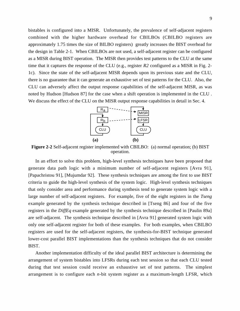
bistables is configured into a MISR. Unfortunately, the prevalence of self-adjacent registers
combined with the higher hardware overhead for CBILBOs (CBILBO registers are
approximately 1.75 times the size of BILBO registers) greatly increases the BIST overhead for
the design in Table 2-1. When CBILBOs are not used, a self-adjacent register can be configured
as a MISR during BIST operation. The MISR then provides test patterns to the CLU at the same
time that it captures the response of the CLU (e.g., register R2 configured as a MISR in Fig. 2-
1c). Since the state of the self-adjacent MISR depends upon its previous state and the CLU,
there is no guarantee that it can generate an exhaustive set of test patterns for the CLU. Also, the
CLU can adversely affect the output response capabilities of the self-adjacent MISR, as was
noted by Hudson [Hudson 87] for the case when a shift operation is implemented in the CLU .
We discuss the effect of the CLU on the MISR output response capabilities in detail in Sec. 4.
Ra
Rb
CLU CLU
MISR
LFSR
(a) (b)
Figure 2-2 Self-adjacent register implemented with CBILBO: (a) normal operation; (b) BISToperation.
In an effort to solve this problem, high-level synthesis techniques have been proposed that
generate data path logic with a minimum number of self-adjacent registers [Avra 91],
[Papachristou 91], [Mujumdar 92]. These synthesis techniques are among the first to use BIST
criteria to guide the high-level synthesis of the system logic. High-level synthesis techniques
that only consider area and performance during synthesis tend to generate system logic with a
large number of self-adjacent registers. For example, five of the eight registers in the Tseng
example generated by the synthesis technique described in [Tseng 86] and four of the five
registers in the DiffEq example generated by the synthesis technique described in [Paulin 89a]
are self-adjacent. The synthesis technique described in [Avra 91] generated system logic with
only one self-adjacent register for both of these examples. For both examples, when CBILBO
registers are used for the self-adjacent registers, the synthesis-for-BIST technique generated
lower-cost parallel BIST implementations than the synthesis techniques that do not consider
BIST.
Another implementation difficulty of the ideal parallel BIST architecture is determining the
arrangement of system bistables into LFSRs during each test session so that each CLU tested
during that test session could receive an exhaustive set of test patterns. The simplest
arrangement is to configure each n-bit system register as a maximum-length LFSR, which

10
generates 2n-1 different test patterns (logic can easily be added to the LFSR so that it generates
all 2n different patterns [McCluskey 86]). This is not an acceptable solution, however, when a
single CLU is fed by multiple system registers (see CLU2 in Fig. 2-1). In this case, the total
number of different test patterns, P, that can be applied to the CLU is the least common multiple
of the periods of the individual LFSRs. For n maximum-length LFSRs, where LFSR i has bibistables and b1 ≤ b2 ≤ ... ≤ bn:
(2bn - 1) ≤ P ≤ (2b1 - 1) (2b2 - 1) (2b3 - 1) ... (2bn-1 - 1)
P < 2b1+b2+b3+...+bn-1
The maximum value for P can only be achieved when the periods of the n LFSRs are mutually
prime. In data path logic, where a single CLU is often fed by n b-bit system registers, we have
the worst-case scenario:
P = 2b - 1 << 2nb
A better solution for providing a nearly exhaustive set of test patterns to each CLU is to
configure the bistables on the inputs of each CLU being tested during a given test session into a
single, maximum-length LFSR. Figure 2-3 illustrates this solution by showing one way to
configure the registers of Fig. 2-1 into LFSRs and MISRs for each of the two required test
sessions. During the first test session (Fig. 2-1b and 2-3a), registers R1 and R2 are configured
into a single maximum-length LFSR in order to provide an exhaustive set of test patterns to
CLU4. Registers R3, R4, and R5 are configured into a MISR to capture the output responses of
CLU3, CLU4, and CLU5. During the second test session (Fig. 2-1c and 2-3b), R2, which is
implemented with a CBILBO register, is configured with R3, R4, and R5 into a single LFSR in
order to test CLU2. The second set of R2 bistables are configured with R1 into a MISR, which
captures the output responses of CLU1 and CLU2. The signal lines in Fig. 2-3 represent the
additional interconnections required for BIST operation. Each block of feedback logic (f1, f2,
and f3) consists of a tree of one or more exclusive-OR gates that implements the polynomial of
the associated LFSR or MISR. The arrangement of the registers during BIST operation (R1 ®
R2 ® R3 ® R4 ® R5) was chosen because it minimizes the amount of BIST interconnection
and feedback logic.
11
MISRLFSR
R1 R5R3 R4
R1 R2 R5R3 R4
R2
f2
MISR LFSR
(a)
(b)
f1
f1f3
Figure 2-3 LFSR and MISR configurations for Fig. 2-1: (a) first test session; (b) second testsession.
Unfortunately, the parallel BIST architecture illustrated in Fig. 2-3 can, in practice, be
extremely complicated and costly to implement. In our discussion, we have ignored how to
configure LFSRs to drive the input signals (primary input signals and control signals) of the data
path logic during BIST operation. Considering these signals could greatly complicate the
configurations of the LFSRs during each test session, particularly if a single state machine
generates all of the control signals for the data path logic. Also, Fig. 2-1 is a relatively simple
data path design example. More complicated data path designs, or non-BIST scan path
arrangement requirements, such as minimizing test time for deterministic stuck-at tests as
described in [Gupta 91] and [Narayanan 92], could greatly increase both the hardware overhead
and the total self-test time for the parallel BIST architecture. Table 2-1 provides a hint of how
complicated the parallel BIST architecture could be for a real design. For example, test session
seven in Table 2-1 shows that the combinational logic feeding register 18 is fed by the outputs of
19 different registers. When these 19 registers are configured into a single, maximum-length
LFSR, 2b-1 different test patterns are applied to the CLU, where b is the total number of bistables
in the 19 registers. Subsets of these 19 registers must be combined with other registers to create
the LFSRs for the remaining eleven test sessions. As the number of test sessions increases, the
BIST control logic and the LFSR interconnection logic for the design can become very
complicated.
The synthesis technique described in Sec. 3 addresses one of the implementation difficulties
of parallel BIST architectures by generating system logic that has a minimum number of self-
adjacent registers. However, the data in Table 2-1 shows that complicated register
interconnections in the system logic can greatly complicate the LFSR configurations required for
a parallel BIST architecture. This issue must be addressed by synthesis techniques before
extensive use of the parallel BIST architecture is practical. To that end, we have investigated
more simple TPG and ORA configuration schemes, such as those found in the circular BIST

12
architecture. The circular BIST architecture is described in Sec. 2.2 and new synthesis
techniques for this architecture are described in Secs. 4 and 5.
2.2 CIRCULAR BIST ARCHITECTURE
Circular BIST is a low overhead, embedded BIST architecture that provides at-speed self-test
operation. Circular BIST has lower area overhead than parallel BIST because it has simpler
BIST control logic and interconnection logic, which also simplifies and speeds the
implementation process. The circular BIST architecture was first introduced as simultaneous
self-test (SST) by Bardell and McAnney [Bardell 82]. It was later described in slightly different
forms by Stroud [Stroud 88] and Krasniewski [Krasniewski 89]. Figure 2-4 illustrates the
circular BIST architecture for the data path logic in Fig. 2-1a. During BIST operation, all system
bistables are configured into a single MISR as shown in Fig. 2-4b. At each clock cycle during
BIST operation, the outputs of all CLUs in the design are captured in a single MISR, and the
outputs of the MISR provide test patterns to the CLUs. The circular BIST architecture requires
little BIST control logic since there is only one test session during which a single MISR
simultaneously performs the TPG and ORA operations. The problems of register self-adjacency
and LFSR configuration discussed in Sec. 2.1 for the parallel BIST architecture are not
applicable to circular BIST. However, since the CLUs in the circular BIST architecture are
simultaneously tested by a single, self-adjacent MISR, the pattern generation and response
analysis capabilities of self-adjacent MISRs must be analyzed to ensure an effective self-test
operation. These issues are discussed in Sec. 4.1 and are addressed by our synthesis for scan
dependence techniques described in Secs. 4.2 and 5.
Since slightly different versions of the circular BIST architecture have been described in
[Bardell 82], [Stroud 88], and [Krasniewski 89], we state here our assumptions concerning the
circular BIST architecture implemented in our synthesized designs. First, we assume that all
bistables in the design are included in the MISR during BIST operation. Other architectures
([Krasniewski 89], [Stroud 88]) allow some bistables to be configured in the normal mode during
BIST operation in order to reduce the BIST overhead, but there is evidence that this can reduce
the observability of the logic feeding those bistables [Kim 88]. Second, we assume that every
system bistable is an edge-triggered flip-flop that can be configured to perform normal, shift, and
MISR operations. A reset mode of operation is optional since the bistables can be controlled
through the shift mode of operation. Using flip-flops simplifies the discussion of the synthesis
techniques. Similar synthesis techniques can be applied if the double-latch, level-sensitive scan
design method is used to implement the system bistables as described in [Bardell 82], but we do
not discuss these techniques in this dissertation. Finally, we assume that the MISR feedback
logic is simply a direct connection from the output of the last bistable in the MISR to the input of

13
the first bistable. A reconfigurable register design that supports these operations is described in
Sec. 2.3.
CLU3
PI PI
CLU4 CLU5
PI
CLU2
PI PIPO
CLU1
R1 R2
MISR
R1 R5R3 R4R2
f
R3 R4 R5
(a) (b)
Figure 2-4 Circular BIST architecture: (a) normal operation; (b) BIST register configuration.
2.3 RECONFIGURABLE REGISTER DESIGN
The distinguishing characteristic of embedded BIST architectures is that the system bistables
can be configured to perform both normal operation (parallel load) as well as test operations such
as serial shift, TPG, and ORA. The test operations that must be supported by each bistable
depend upon the embedded BIST architecture used. The Circular Self-Test Path architecture
[Krasniewski 89], for example, does not require that the system bistables perform a serial shift
operation. The built-in logic block observer (BILBO) register [Konemann 79] is often used in
embedded BIST architectures and implements normal, synchronous reset, serial shift, TPG, and
ORA modes of operation.
Figure 2-5 illustrates a reconfigurable register design that can be used for both the parallel
BIST and circular BIST architectures. The register implementation is not necessarily optimal.
Its purpose is to more easily illustrate the BIST operations. In Secs. 4 and 5, we use Fig. 2-5 to
illustrate scan dependence and our synthesis techniques. Figure 2-5a shows the register
configuration, where each bistable in the register is implemented as shown in Fig. 2-5b. The
bistable could also be implemented with a dual-port latch, such as the design specified for theSST technique [Bardell 82]. The Qi-1 input to the first bistable (bistable B1) in the register is
determined by BIST mode select signal BIST, and is either the scan data input (SDI) signal for
shift operation or the output of the MISR feedback logic for MISR operation or LFSR operation.
For circular BIST architectures, since a separate TPG operation is not required, signal BIST canbe replaced by signal T1, resulting in four possible modes of operation: reset, shift, normal, and
MISR. Test mode select signals T1 and T2 determine the D input to each bistable in the register,
as specified in Fig. 2-5c, where Zi is the system logic input to bistable Bi.

14
Normal
Mode
0 ResetShift or
MISR
T1
Z Å
T2
0001
1011
01
MUXG
Q
BIST
T1T2
Z
Q
Z
Q
Z
Q
&Å 1D
C1
T1
T2
&
SDO
Å
Z 1 2 i n
1 2 i n
Di
Zi
i
Z i
Q iQi-1
Q i-1
Qi-1
Di
01
LFSR
SDIB 1 B 2 B i Bn
(a) (b) (c)
Figure 2-5 Reconfigurable register: (a) bistable interconnections; (b) reconfigurable bistable;(c) modes of operation.
For circular BIST architectures and for parallel BIST architectures with self-adjacent
registers that are not implemented with CBILBOs (i.e., for self-adjacent MISRs), the MISR
operation must simultaneously provide both sufficient test patterns and accurate output response
analysis. It has been proven that, when the Z inputs are independent of the state of an n-bit
MISR, the MISR generates test patterns that are similar in behavior to random patterns
[Krasniewski 89], [Kim 88]. Specifically, as P goes to infinity, where P is the number of test
patterns applied during BIST operation, the probability of the MISR being in any one of the 2n
possible states is 2-n. The Z inputs to a self-adjacent MISR, however, are a function of the state
of the MISR. Simulation results presented in [Kim 88] and [Stroud 88] indicate that the MISR
test pattern characteristics are not significantly different from random patterns when the Z inputs
depend upon the state of the MISR. It is not clear whether a MISR implemented with a primitivepolynomial [Kim 88] produces any better patterns than a MISR implemented with a single Qn
feedback connection [Krasniewski 89].
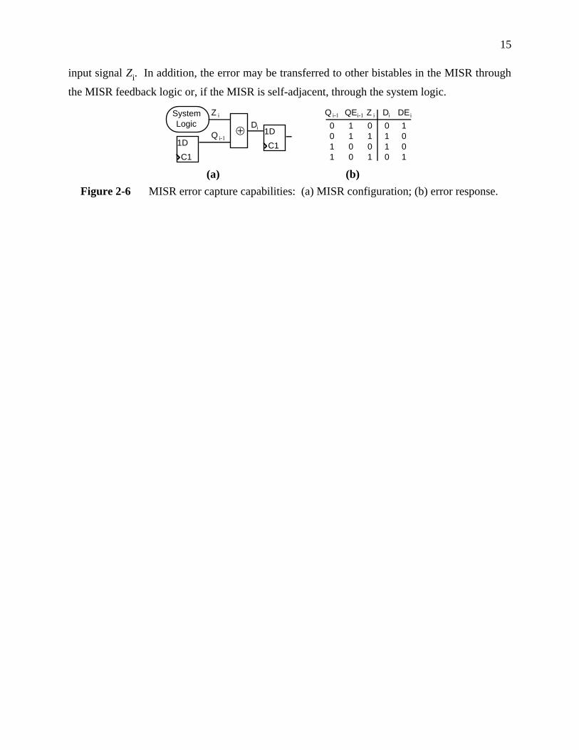
Figure 2-6a shows a portion of the reconfigurable register during MISR operation to illustrateits error capture capabilities. During MISR operation, the input to each bistable, Di, is the
exclusive-OR of the output of the previous bistable in the MISR, Qi-1, and the system logic input
to the bistable, Zi. At each clock cycle, an error in either Zi or Qi-1 is observable at Di (i.e.,
captured in bistable Bi) regardless of the state of the error-free signal. Figure 2-6b is a truth table
for signals Di (Di = Qi-1 Å Zi) and DEi (DEi = QEi-1 Å Zi), where QEi-1 is the faulty version of
signal Qi-1. Figure 2-6b shows that, regardless of the state of signal Zi, Di differs from DEi, so
when Zi is fault-free, an error in Qi-1 is always captured in bistable Bi. Because the exclusive-OR
operation is symmetric, the same is true when Qi-1 is fault-free and Zi is faulty. However, errors
in both signals Zi and Qi-1 in a single clock cycle are not observable at Di. Thus, once captured
in a bistable of the MISR, an error is transferred from one bistable (Qi-1) to the next (Qi) at each
clock cycle as long as it is not masked by a simultaneous error in the corresponding system logic
15
input signal Zi. In addition, the error may be transferred to other bistables in the MISR through
the MISR feedback logic or, if the MISR is self-adjacent, through the system logic.
Å 1D
C11D
C1
Q i-1
Di 0011
1100
0101
0110
1001
QE DEZ i DiZ iQ i-1 i-1 iSystemLogic
(a) (b)
Figure 2-6 MISR error capture capabilities: (a) MISR configuration; (b) error response.

16
3 ALLOCATION AND BINDING FOR PARALLEL BIST
The interconnection of system logic registers can greatly affect the area overhead of parallel
BIST architectures and the effectiveness of the TPGs and ORAs as was shown in Sec. 2.1.
System register interconnect is an issue that must be addressed during high-level synthesis, when
variables in the behavioral description are mapped to specific registers in the structural
description. Little work has been done in the area of high-level synthesis-for-testability.
Recently, high-level synthesis algorithms for non-scan and partial-scan architectures have been
given [Lee 93]. These algorithms are not well-suited for parallel BIST architectures, however,
because they favor the generation of self-adjacent registers since self-adjacent bistables, which
can occur in self-adjacent registers, are considered easier to test by sequential automatic test
pattern generation tools [Cheng 89]. High-level synthesis procedures that discourage the
generation of self-adjacent registers are described in [Avra 91], [Papachristou 91], and
[Mujumdar 92]. The technique described in [Papachristou 91] generates data path logic with no
self-adjacent registers, but may increase the latency of the functional operation in order to do
this. The module and register binding algorithm given in [Mujumdar 92] discourages, but does
not prevent, the generation of self-adjacent registers.
This section provides an overview of our high-level synthesis-for-BIST technique, first
described in [Avra 90], that takes as input a scheduled data flow description of the system logic
and, without increasing the latency of the description, generates a parallel BIST data path
structure with a minimum number of self-adjacent registers. A more detailed description of the
technique is given in [Avra 91]. The synthesis procedure consists of first mapping the input data
flow description to a register conflict graph. The nodes of the graph are then colored using a
node coloring algorithm that is guided by design implementation costs such as interconnection
area and multiplexer size. Finally, the colored graph is mapped to hardware. A simple constraint
imposed on the register conflict graph prevents the register binding algorithm from creating self-
adjacent registers in the generated data path logic, thereby reducing the area overhead of the
parallel BIST architecture when self-adjacent registers are implemented with CBILBO registers.
We also incorporate a novel register allocation technique that allows the register binding
algorithm increased flexibility in synthesizing an efficient hardware implementation.
Section 3.1 is background material and provides an overview of the operations performed
during high-level synthesis. In Sec. 3.2, we describe the register conflict graph, focusing on the
features that make our high-level synthesis procedure unique. Section 3.3 describes the register
binding algorithm that is implemented in our synthesis tool and compares designs generated by
our tool with designs generated by other synthesis techniques. Section 3.4 summarizes our
contributions in high-level synthesis for parallel BIST.
17
3.1 HIGH-LEVEL SYNTHESIS TASKS
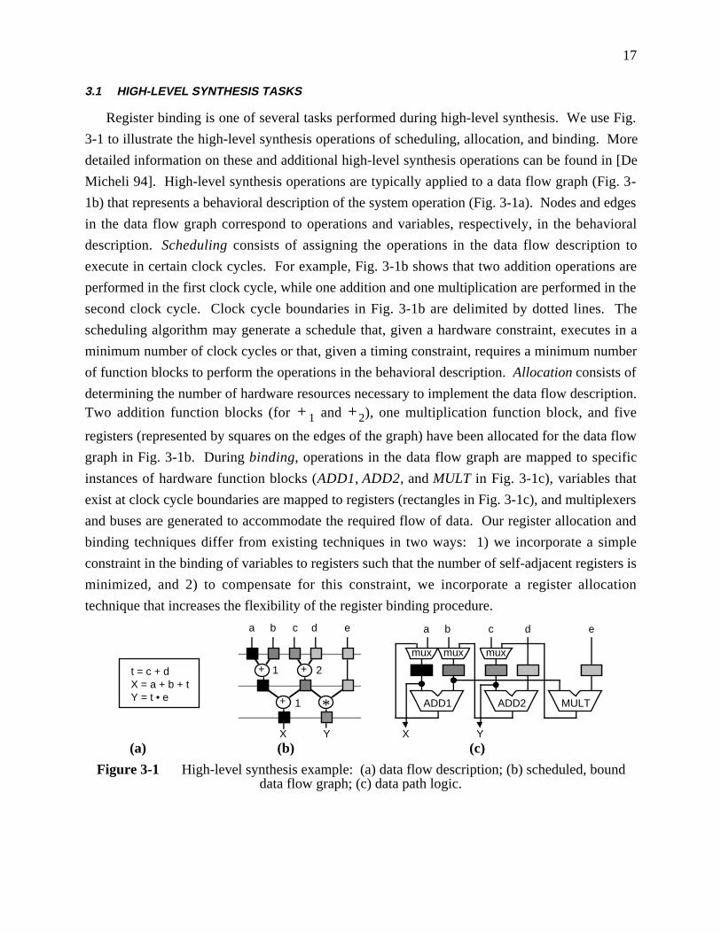
Register binding is one of several tasks performed during high-level synthesis. We use Fig.
3-1 to illustrate the high-level synthesis operations of scheduling, allocation, and binding. More
detailed information on these and additional high-level synthesis operations can be found in [De
Micheli 94]. High-level synthesis operations are typically applied to a data flow graph (Fig. 3-
1b) that represents a behavioral description of the system operation (Fig. 3-1a). Nodes and edges
in the data flow graph correspond to operations and variables, respectively, in the behavioral
description. Scheduling consists of assigning the operations in the data flow description to
execute in certain clock cycles. For example, Fig. 3-1b shows that two addition operations are
performed in the first clock cycle, while one addition and one multiplication are performed in the
second clock cycle. Clock cycle boundaries in Fig. 3-1b are delimited by dotted lines. The
scheduling algorithm may generate a schedule that, given a hardware constraint, executes in a
minimum number of clock cycles or that, given a timing constraint, requires a minimum number
of function blocks to perform the operations in the behavioral description. Allocation consists of
determining the number of hardware resources necessary to implement the data flow description.Two addition function blocks (for +1 and +2), one multiplication function block, and five
registers (represented by squares on the edges of the graph) have been allocated for the data flow
graph in Fig. 3-1b. During binding, operations in the data flow graph are mapped to specific
instances of hardware function blocks (ADD1, ADD2, and MULT in Fig. 3-1c), variables that
exist at clock cycle boundaries are mapped to registers (rectangles in Fig. 3-1c), and multiplexers
and buses are generated to accommodate the required flow of data. Our register allocation and
binding techniques differ from existing techniques in two ways: 1) we incorporate a simple
constraint in the binding of variables to registers such that the number of self-adjacent registers is
minimized, and 2) to compensate for this constraint, we incorporate a register allocation
technique that increases the flexibility of the register binding procedure.
ADD1
mux
ADD2 MULT
+ 1 2
1
X Y
a b c d e a b c d e
X Y
mux mux
+
+t = c + dX = a + b + tY = t • e
*
(a) (b) (c)
Figure 3-1 High-level synthesis example: (a) data flow description; (b) scheduled, bounddata flow graph; (c) data path logic.

18
3.2 REGISTER CONFLICT GRAPH
Our register allocation and binding operations are applied to a register conflict graph data
structure. Each node in the register conflict graph represents an edge from the data flow graph
that crosses a clock cycle boundary. An edge between two nodes in the register conflict graph
indicates that the two variables associated with those nodes cannot be stored in the same register.
Register binding consists of assigning a color to each of the nodes in the register conflict graph
such that adjacent nodes have different colors. All nodes with the same color can be mapped to
the same register in the final implementation. This is analogous to the techniques described in
[Tseng 86] and [Paulin 89b], where a register compatibility graph is created, clique partitioning
is performed, and all nodes in the same clique are assigned to the same register. Figure 3-2b
illustrates the typical conflict graph-based register allocation and binding procedures for the data
flow graph of Fig 3-1b. Figure 3-2a is the same data flow graph as Fig. 3-1b except that the
register binding information (colored squares on clock cycle boundaries) has been removed.
Nine nodes, corresponding to data flow graph variables a, b, c, d, e, s, t, X, and Y, are created in
the register conflict graph. Edges are added between nodes whose variables cannot be assigned
to the same register. For example, variables a, b, c, d, and e all exist at the first clock cycle in the
data flow graph and must therefore all be assigned to different registers, so their nodes form a
clique in the register conflict graph. One possible coloring of the register conflict graph is shown
in Fig. 3-2b, where the different colors correspond to different registers in the structural
implementation.
We define register allocation as the method used to determine how many nodes to create in
the register conflict graph. Our register allocation procedure is illustrated in Fig. 3-2c and is
unique in that it creates multiple nodes in the register conflict graph for a single variable in the
data flow graph under three conditions: delayed values, multiple targets, and multiple sources.
We do this in order to increase the flexibility of the register binding algorithm in mapping
variables to non-self-adjacent registers. For the delayed values situation, a node is added to the
register conflict graph for each clock cycle in a variable’s lifetime. This means that the variable
could be transferred from one register to another rather than held in a single register for its entire
lifetime as most register allocation techniques require. The delayed values allocation scheme is
illustrated by nodes e and De in Fig. 3-2c, which both represent variable e from the data flow
description. Note that there is no edge between nodes e and s since they exist at different clock
cycles, but there is an edge between nodes De and s. The delayed values consideration is an
extension of the technique first introduced in [Paulin 89b], where it was shown that when a
register is allocated for the first clock cycle of a variable’s lifetime, and another register is
allocated for the remaining clock cycles of its lifetime, interconnect cost can sometimes be
reduced. Multiple targets means that a node is added to the register conflict graph for each

19
output of an operation that crosses a clock cycle boundary. For example, nodes t1 and t2 in Fig.
3-2c both represent the variable t in Fig. 3-2a. Node t1 represents the input to the addition
operation, and node t2 represents the input to the multiplication operation. No edge is added
between nodes t1 and t2 because they could be assigned to the same register since they represent
the same variable. Multiple sources, which is not shown in Fig. 3-2c, is similar to multiple
targets except that a node is added to the conflict graph for each operation input that represents a
single variable. This situation occurs when the input to an operation is assigned a value in
multiple, mutually-exclusive branches of a conditional statement. The multiple sources situation
is described in detail in [Avra 91].
+ 1 2
1+
+
De
t1a
bc
de Y
X
a b c d e
Dets
X Y s
ta
bc
de Y
X
s
t2
*
(a) (b) (c)
Figure 3-2 Register conflict graph example: (a) data flow graph from Fig. 3-1b; (b) typicalregister conflict graph; (c) our register conflict graph.
Conflict edges are edges in the register conflict graph that specify that the variables
associated with the adjacent nodes cannot be assigned to the same register. We call the edges
shown in the register conflict graphs in Fig. 3-2 schedule conflict edges because the conflict that
exists between the adjacent nodes is due to the schedule specified for the data flow graph.
Schedule conflict edges therefore maintain the functionality of the system logic. Our register
binding algorithm is unique in that we include an additional type of conflict edge in the register
conflict graph that maintains the testability of the generated system logic. Testability conflict
edges are added between two nodes when one node represents a variable that is an input to a
function block and the other node represents a variable that is an output of the same function
block. For example, Fig. 3-3b is the register conflict graph for Fig. 3-3a, showing just thetestability conflict edges for the three function blocks, +1, +2, and *. Note that an edge is added
between nodes a and s and between nodes a and X because both s and X are outputs of the same
function block. Node e has no adjacent testability conflict edges because it is not an input or an
output of any function block. Testability conflict edges require that the inputs and the outputs of
a function block be assigned to different registers, and this guarantees that no self-adjacent
registers will be synthesized. One situation requires the use of a self-adjacent register: when two
operations in consecutive clock cycles in the data flow graph are assigned to a single function
block and the output of one operation is the input to the other (see variable s in Fig. 3-3a). In this
case, the node that is associated with both the input and the output of the function block is
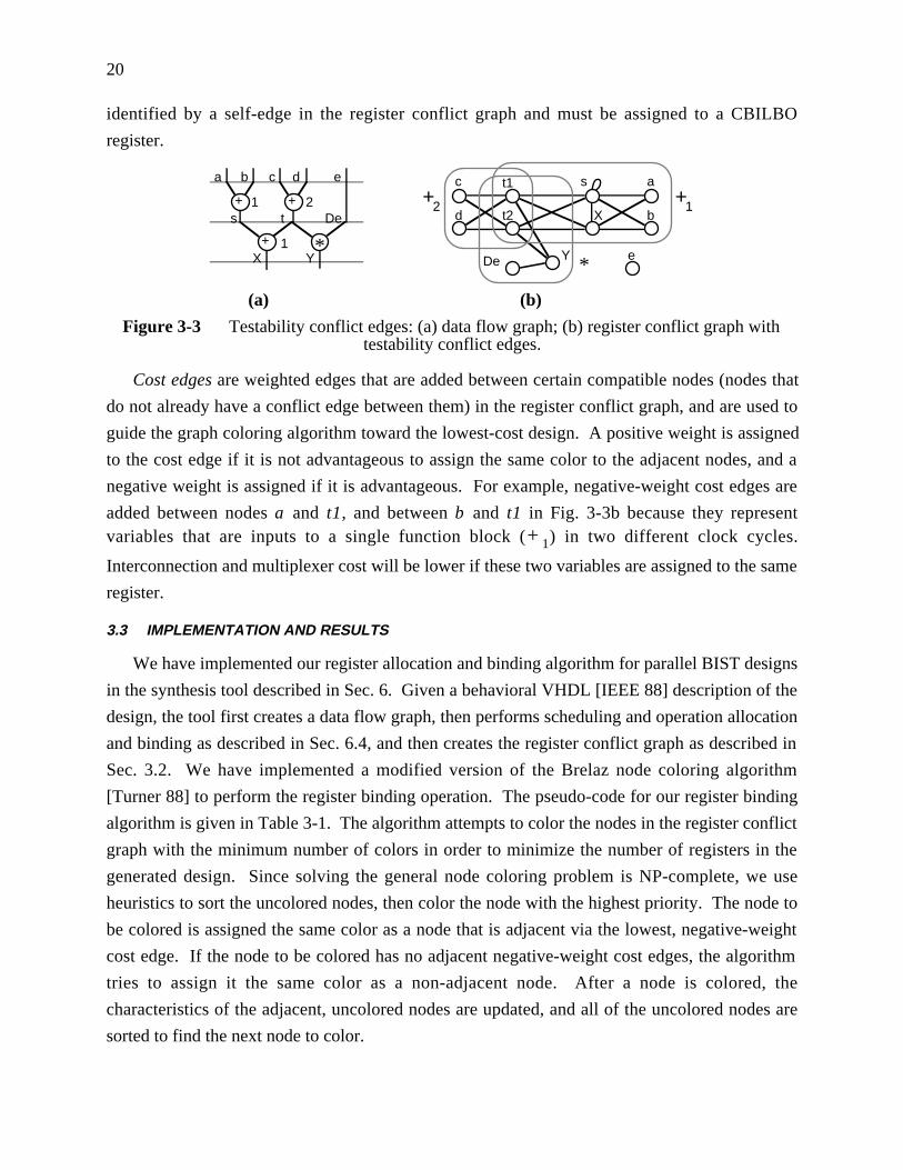
20
identified by a self-edge in the register conflict graph and must be assigned to a CBILBO
register.
De
t1 a
b
c
d
Y
X
s
t2+2 +1
*
+ 1 2
1+
+
a b c d e
Dets
X Y* e
(a) (b)
Figure 3-3 Testability conflict edges: (a) data flow graph; (b) register conflict graph withtestability conflict edges.
Cost edges are weighted edges that are added between certain compatible nodes (nodes that
do not already have a conflict edge between them) in the register conflict graph, and are used to
guide the graph coloring algorithm toward the lowest-cost design. A positive weight is assigned
to the cost edge if it is not advantageous to assign the same color to the adjacent nodes, and a
negative weight is assigned if it is advantageous. For example, negative-weight cost edges are
added between nodes a and t1, and between b and t1 in Fig. 3-3b because they representvariables that are inputs to a single function block (+ 1) in two different clock cycles.
Interconnection and multiplexer cost will be lower if these two variables are assigned to the same
register.
3.3 IMPLEMENTATION AND RESULTS
We have implemented our register allocation and binding algorithm for parallel BIST designs
in the synthesis tool described in Sec. 6. Given a behavioral VHDL [IEEE 88] description of the
design, the tool first creates a data flow graph, then performs scheduling and operation allocation
and binding as described in Sec. 6.4, and then creates the register conflict graph as described in
Sec. 3.2. We have implemented a modified version of the Brelaz node coloring algorithm
[Turner 88] to perform the register binding operation. The pseudo-code for our register binding
algorithm is given in Table 3-1. The algorithm attempts to color the nodes in the register conflict
graph with the minimum number of colors in order to minimize the number of registers in the
generated design. Since solving the general node coloring problem is NP-complete, we use
heuristics to sort the uncolored nodes, then color the node with the highest priority. The node to
be colored is assigned the same color as a node that is adjacent via the lowest, negative-weight
cost edge. If the node to be colored has no adjacent negative-weight cost edges, the algorithm
tries to assign it the same color as a non-adjacent node. After a node is colored, the
characteristics of the adjacent, uncolored nodes are updated, and all of the uncolored nodes are
sorted to find the next node to color.

21
Table 3-1 Register binding algorithm for parallel BIST register conflict graph.
Color_Nodes (Register Conflict Graph)While (Some Nodes Uncolored) do
Sort Uncolored Nodes According to:1. Has Self-Adjacent Constraint Edge2. Has Least Number Available Colors3. Has Most Constraint Edges4. Has Least Sum Of Cost Edges
Select Highest-Priority NodeColor With Lowest-Cost Adjacent ColorUpdate Uncolored, Adjacent Nodes
end While
The data path logic in Fig. 3-1c was generated by applying the register binding algorithm in
Table 3-1 to the data flow graph in Fig. 3-1b. As shown by the self-edge in Fig. 3-3b, node s
must be assigned to a self-adjacent register, so the register binding algorithm selected node s to
color first. The register associated with node s (and nodes a and X since they were assigned the
same color) is implemented as a CBILBO register and is the only self-adjacent register in the
generated design.
Table 3-2 compares the results of our register allocation and binding technique, called
RALLOC, with the results published in [Tseng 86], [Pangrle 88], [Paulin 89a], and [Papachristou
91] for two design examples, Tseng [Tseng 86] and DiffEq [Paulin 89a]. The design cost
estimates of the synthesized hardware are based on the number of self-adjacent (SA) registers,
non-self-adjacent (NSA) registers, multiplexer inputs (mux), interconnections (int), and control
signals (ctl), and are computed as follows:
cost1 = 14 • (NSA reg) + 14 • (SA reg) + mux + int + ctl
cost2 = 20 • (NSA reg) + 35 • (SA reg) + mux + int + ctl
For the first design cost estimate, cost1, all registers have the same cost. This represents the cost
of data path logic with no BIST or scan circuitry. The second design cost estimate, cost2,
represents the cost of a parallel BIST implementation of the data path logic. In this case, non-
self-adjacent registers are implemented with the register design shown in Fig. 2-5a, which is
estimated to be approximately 20 times the cost of a multiplexer input, and self-adjacent
registers are implemented with the higher-cost CBILBO register.
The goal of the synthesis techniques presented in [Tseng 86], [Pangrle 88], and [Paulin 89a]
is to minimize the area of the generated data path logic. Since they do not consider testability
during the synthesis process, their implementations, understandably, have a higher number ofself-adjacent registers, which partially accounts for the higher values for cost2 in Table 3-2. Both
our synthesis technique and the technique described in [Papachristou 91] attempt to minimize the
cost of the design while preventing the generation of self-adjacent registers. By comparing our

22
technique with techniques that do not consider testability, we show the difference between
synthesis-for-BIST, where the design is optimized for a particular BIST architecture, and BIST
synthesis, where BIST circuitry is added to a design that has been synthesized for area and
performance.
For both examples in Table 3-2, our technique generated the lowest-cost parallel BIST
implementation (cost2). Our technique also generated designs with the minimum number of
registers, showing that the additional testability constraint edge in the register conflict graph didnot require an increase in the number of registers for these examples. The cost1 column in Table
3-2 shows that, if parallel BIST is not implemented, the costs of the data path designs generated
by our technique are comparable to the costs of the other designs.
Table 3-2 Comparison of synthesis procedures on Tseng [Tseng 86] and DiffEq [Paulin 89a]data flow descriptions.
Name NSA reg SA reg mux int ctl cost1 cost2Tseng
[Tseng 86] 3 5 15 31 23 181 304[Pangrle 88] 4 3 11 26 18 153 240[Papachristou
91]8 0 12 28 20 172 220
RALLOC 4 1 16 29 21 136 181
DiffEq[Pangrle 88] 1 5 17 34 23 158 269[Paulin 89a] 1 4 19 35 24 148 238RALLOC 4 1 22 38 27 157 202
3.4 CONTRIBUTIONS
We have developed and implemented a new register allocation and binding technique that
generates data path logic optimized for the parallel BIST architecture given a scheduled,
operation-bound data flow description of the design. A simple testability constraint edge added
to the register conflict graph is used to guarantee that the generated data path logic has a
minimum number of self-adjacent registers. This testability requirement can be easily adapted to
existing register allocation and binding procedures. We have also developed and implemented
new techniques for register allocation (delayed values, multiple targets, and multiple sources)
that provide the register binding procedure increased flexibility in synthesizing an efficient
hardware implementation while minimizing the number of self-adjacent registers.
Results show that, when the parallel BIST architecture is used, addressing register self-
adjacency during high-level synthesis results in a lower-cost design. For both examples
evaluated, our technique synthesized the lowest-cost, parallel BIST design. In addition, for both
23
examples, if parallel BIST is not implemented, the costs of the data path designs generated by
our technique are comparable to the costs of the other designs. This shows that, even if BIST
and scan circuitry is not included in the design, minimizing the number of self-adjacent registers
during synthesis does not necessarily increase, and may even reduce, the cost of the generated
data path logic.

24
4 SYNTHESIS FOR SCAN DEPENDENCE
Performance degradation, area overhead, and test transparency (the fraction of defects not
detected by the test) are three issues that must be addressed when synthesizing a built-in self-
testable design. The register allocation and binding technique described in Sec. 3 reduces the
area overhead of a parallel BIST design without increasing test transparency or the number of
clock cycles required to execute the data path function. However, since there is additional BIST
logic associated with each system register in the data path, the clock period may have to be
increased, resulting in slower performance. In this section, we describe a new synthesis
technique, applied to the bistables in the design, that relies on the sharing of system logic and test
logic to reduce the area and improve the performance without increasing the test transparency of
BIST architectures, such as circular BIST and parallel BIST, that make use of embedded MISRs.
This technique was first described in [Avra 93]. A more detailed description of the technique is
given in [Avra 94a].
The goal of our synthesis technique is to arrange the system bistables into scan paths so that
some of the BIST and scan logic is shared with the system logic. Logic sharing is possible when
scan dependence is introduced in the design. Other BIST design techniques attempt to avoid all
types of scan dependence because it can increase the test transparency of embedded MISRs. We
show that introducing certain types of scan dependence in embedded MISRs can reduce the
overhead and the test transparency, and we describe a synthesis technique that maximizes the
amount of this beneficial scan dependence. The synthesis technique first analyzes the CUT
feeding the MISR, then based on the CUT function, it modifies the MISR function in order to
reduce the amount of aliasing during BIST operation. We have implemented this synthesis
technique in our synthesis-for-test design tool (described in Sec. 6) and we present fault
simulation, layout area, and delay results for circular BIST versions of benchmark circuits that
have been synthesized with our technique.
Section 4.1 provides a formal definition of scan dependence and includes design examples
that illustrate its advantages and disadvantages. In Sec. 4.2, we describe design techniques for
beneficial scan dependence and show how to introduce it in the design by arranging the system
bistables into MISRs. Section 4.3 contains fault simulation and overhead results of several
benchmark circuits generated with our synthesis technique and optimized for the circular BIST
architecture described in Sec. 2.2. Section 4.4 summarizes our contributions in the area of scan
dependence.
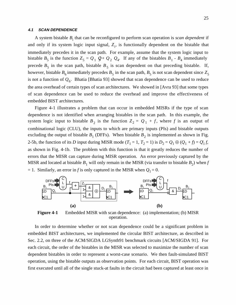
25
4.1 SCAN DEPENDENCE
A system bistable Bi that can be reconfigured to perform scan operation is scan dependent if
and only if its system logic input signal, Zi, is functionally dependent on the bistable that
immediately precedes it in the scan path. For example, assume that the system logic input tobistable B5 is the function Z5 = Q 1 Q'3 + Q 2 Q4. If any of the bistables B1 - B4 immediately
precede B5 in the scan path, bistable B 5 is scan dependent on that preceding bistable. If,
however, bistable B6 immediately precedes B5 in the scan path, B5 is not scan dependent since Z5
is not a function of Q6. Bhatia [Bhatia 93] showed that scan dependence can be used to reduce
the area overhead of certain types of scan architectures. We showed in [Avra 93] that some types
of scan dependence can be used to reduce the overhead and improve the effectiveness of
embedded BIST architectures.
Figure 4-1 illustrates a problem that can occur in embedded MISRs if the type of scan
dependence is not identified when arranging bistables in the scan path. In this example, thesystem logic input to bistable B 2 is the function Z2 = Q 1 + f , where f is an output of
combinational logic (CLU), the inputs to which are primary inputs (PIs) and bistable outputsexcluding the output of bistable B1 (DFFs). When bistable B2 is implemented as shown in Fig.
2-5b, the function of its D input during MISR mode (T1 = 1, T2 = 1) is D2 = Q1 Å (Q1 + f) = Q1' f,
as shown in Fig. 4-1b. The problem with this function is that it greatly reduces the number of
errors that the MISR can capture during MISR operation. An error previously captured by theMISR and located at bistable B1 will only remain in the MISR (via transfer to bistable B2) when f
= 1. Similarly, an error in f is only captured in the MISR when Q1 = 0.
&Å 1D
C1
&1D
C1
+f
D2Q1
Z2
1D
C1
&1D
C1
D2
f
1
1
Q1
CLU
DFFsPIs
CLU
DFFsPIs B2 B2B1B1
(a) (b)
Figure 4-1 Embedded MISR with scan dependence: (a) implementation; (b) MISRoperation.
In order to determine whether or not scan dependence could be a significant problem in
embedded BIST architectures, we implemented the circular BIST architecture, as described in
Sec. 2.2, on three of the ACM/SIGDA LGSynth91 benchmark circuits [ACM/SIGDA 91]. For
each circuit, the order of the bistables in the MISR was selected to maximize the number of scan
dependent bistables in order to represent a worst-case scenario. We then fault-simulated BIST
operation, using the bistable outputs as observation points. For each circuit, BIST operation was
first executed until all of the single stuck-at faults in the circuit had been captured at least once in
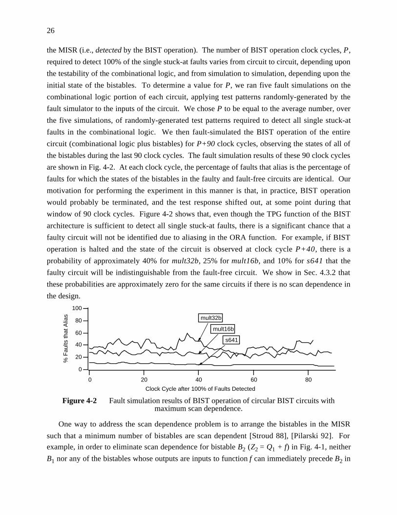
26
the MISR (i.e., detected by the BIST operation). The number of BIST operation clock cycles, P,
required to detect 100% of the single stuck-at faults varies from circuit to circuit, depending upon
the testability of the combinational logic, and from simulation to simulation, depending upon the
initial state of the bistables. To determine a value for P, we ran five fault simulations on the
combinational logic portion of each circuit, applying test patterns randomly-generated by the
fault simulator to the inputs of the circuit. We chose P to be equal to the average number, over
the five simulations, of randomly-generated test patterns required to detect all single stuck-at
faults in the combinational logic. We then fault-simulated the BIST operation of the entire
circuit (combinational logic plus bistables) for P+90 clock cycles, observing the states of all of
the bistables during the last 90 clock cycles. The fault simulation results of these 90 clock cycles
are shown in Fig. 4-2. At each clock cycle, the percentage of faults that alias is the percentage of
faults for which the states of the bistables in the faulty and fault-free circuits are identical. Our
motivation for performing the experiment in this manner is that, in practice, BIST operation
would probably be terminated, and the test response shifted out, at some point during that
window of 90 clock cycles. Figure 4-2 shows that, even though the TPG function of the BIST
architecture is sufficient to detect all single stuck-at faults, there is a significant chance that a
faulty circuit will not be identified due to aliasing in the ORA function. For example, if BIST
operation is halted and the state of the circuit is observed at clock cycle P+40, there is a
probability of approximately 40% for mult32b, 25% for mult16b, and 10% for s641 that the
faulty circuit will be indistinguishable from the fault-free circuit. We show in Sec. 4.3.2 that
these probabilities are approximately zero for the same circuits if there is no scan dependence in
the design.
0
20
40
60
80
100
% F
aults
that
Alia
s
0 20 40 60 80
Clock Cycle after 100% of Faults Detected
mult16b
mult32b
s641
Figure 4-2 Fault simulation results of BIST operation of circular BIST circuits withmaximum scan dependence.
One way to address the scan dependence problem is to arrange the bistables in the MISR
such that a minimum number of bistables are scan dependent [Stroud 88], [Pilarski 92]. For
example, in order to eliminate scan dependence for bistable B2 (Z2 = Q1 + f) in Fig. 4-1, neither
B1 nor any of the bistables whose outputs are inputs to function f can immediately precede B2 in

27
the MISR. Unfortunately, it may not always be possible to create an embedded MISR that has
no scan dependent bistables, particularly in “control-dominated” designs where bistable inputs
are often a function of a significant number of the bistable outputs in the design. Also,
eliminating all scan dependence eliminates opportunities to share system and test logic.
We propose to solve the problem of MISR aliasing due to scan dependence by using a
different MISR mode function for the scan dependent bistables. The MISR function used
depends upon the type of scan dependence. For example, when the system logic for bistable B2
has the general form Z2 = Q1 + f, where B1 immediately precedes B2 in the MISR, we use Q1 Å f
as the MISR function. The Boolean function for the input to B2 is then:
D2 = T1' T2' Q1 + T1' T2 Q1 + T1 T2' (Q1 + f) + T1 T2 (Q1 Å f)
= T1' Q1 + T1 T2' (Q1 + Q1' f) + T1 T2 (Q1 Å f)
= Q1 (T1' + T2' + f') + Q1' (T1 f)
One possible logic implementation for this function is compared with a scan dependence
avoidance implementation in Fig. 4-3. Figure 4-3a shows our implementation, where the MISR
function is D2 = Q1 Å f. The scan dependence avoidance implementation is shown in Fig. 4-3b,
where the MISR function is D2 = Qx Å Z2 = Qx Å (Q1 Å f), Qx is the output of another bistable
in the scan path, and f is not a function of Qx. Both implementations were mapped to LSI Logic
1.0 micron standard cell gates [LSI 91]. Area (in LSI Logic cell units) and delay (f to D2 in
nanoseconds) for the shaded areas of Fig. 4-3 are provided in Table 4-1. Note that the circuit in
Fig. 4-3a performs the shift operation (D2 = Q1) when T1 = T2 = 0, whereas the circuit in Fig. 4-
3b performs a synchronous reset operation (D2 = 0). Note also that bistable B2 in Fig. 4-3a has
greater observability of system logic errors during MISR mode than bistable B2 in Fig. 4-3b. If
bistable B2 is not scan dependent, an error observable at f is only captured in the MISR when Q1
is 0 (i.e., when the error is observable at Z2), whereas if scan dependence is implemented as
shown in Fig. 4-3a, all errors observable at f are captured in the MISR. Greater observability of
system logic errors can reduce the test transparency of the BIST operation.
The disadvantage of scan dependence, as shown in Fig. 4-2, is that it can result in significant
error loss in embedded MISRs if the function for MISR mode is not specifically selected for the
type of scan dependence. The advantage of scan dependence, as shown in Fig. 4-3, is that, when
the MISR function is carefully selected, the delay and area of the test logic for the scan
dependent bistable can sometimes be reduced. Section 4.2 summarizes our synthesis technique,
which first analyzes the combinational logic feeding each system bistable, then based on this
analysis, determines the best arrangement of bistables into MISRs and modifies the MISR
function in order to reduce the amount of aliasing during BIST operation.
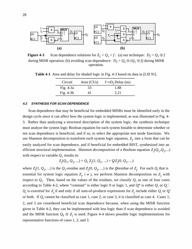
28
&T1
T2&
1D
C1
f
Q1
&T1
T2
&1D
C1
f
Qx
&
1D
C1 Q1
+
Q201
MUXG 0
1 1D
C1
D2Q20
1
MUXG 0
1 1D
C1
D2
(a) (b)
Figure 4-3 Scan dependence solutions for Z2 = Q1 + f : (a) our technique: D2 = Q1 Å f
during MISR operation; (b) avoiding scan dependence: D2 = Qx Å (Q1 Å f) during MISRoperation.
Table 4-1 Area and delay for shaded logic in Fig. 4-3 based on data in [LSI 91].
Circuit Area (CUs) f®D2 Delay (ns)
Fig. 4-3a 33 1.88Fig. 4-3b 41 2.21
4.2 SYNTHESIS FOR SCAN DEPENDENCE
Scan dependence that may be beneficial for embedded MISRs must be identified early in the
design cycle since it can affect how the system logic is implemented, as was illustrated in Fig. 4-
3. Rather than analyzing a structural description of the system logic, the synthesis technique
must analyze the system logic Boolean equation for each system bistable to determine whether or
not scan dependence is beneficial, and if so, to select the appropriate test mode functions. Weuse Shannon decomposition to transform each system logic equation, Zj, into a form that can be
easily analyzed for scan dependence, and if beneficial for embedded BIST, synthesized into anefficient structural implementation. Shannon decomposition of a Boolean equation Zj(Q1,Q2,...)
with respect to variable Q1 results in:
Zj(Q1, Q2, ...) = Q1 Zj(1, Q2, ...) + Q'1 Zj(0, Q2, ...)
where Zj(1, Q2, ...) is the Q1-residue and Zj(0, Q2, ...) is the Q'1-residue of Zj. For each Qi that is
essential for system logic equation Zj, i ¹ j, we perform Shannon decomposition on Zj with
respect to Qi. Then, based on the values of the residues, we classify Qi as one of four cases
according to Table 4-2, where “constant” is either logic 0 or logic 1, and Q*i is either Qi or Q 'i .
Qi is essential for Zj if and only if all sum-of-products expressions for Zj include either Qi or Q 'i
or both. If Qi cannot be classified as case 1, case 2, or case 3, it is classified as case 4. Cases 1,
2, and 3 are considered beneficial scan dependence because, when using the MISR function
given in Table 4-2, they can be implemented with less logic than if scan dependence is avoided
and the MISR function Qk Å Z j is used. Figure 4-4 shows possible logic implementations for
representative functions of cases 1, 2, and 3.

29
Table 4-2 Scan dependence classification of decomposed Boolean equations.
Class Qi-residue Q'i-residue Equation Form MISR Function
Case 1 constant constant Zj = Q*i Dj = Q*i
Case 2 constantnot constant
not constantconstant Zj = (Q*i + f)* Dj = Q*i Å f
Case 3 (Q'i -residue)' (Qi-residue)' Zj = Q*i Å f Dj = Q*i Å f
Case 4 not constant not constant Zj = Qi f + Q'i g AVOID
1D
C11D
C1
&
Å
fT1
Q i D j
1D
C1T1
T2
1D
C1
f
Test Overhead
D j
Q i
01
MUXG 0
1
1D
C1
1D
C1
Q i Dj
&
&
(a) (b) (c)
Figure 4-4 Beneficial scan dependence implementations: (a) case 1: Zj = Qi; (b) case 2: Zj =
Qi + f; (c) case 3: Zj = Qi Å f.
To date, we have not determined a way for system logic equations classified as case-4
equations to benefit, in terms of reduced area and performance overhead, from scan dependence.Therefore, if the Shannon decomposition of Zj with respect to Qi is a case-4 equation, bistable Bi
should not immediately precede bistable Bj in the scan path, otherwise the effectiveness of theMISR will be compromised. To show that this is true, let p and q be the Qi- and Q 'i -residues,
respectively, of Zj (Zj = Qi p + Q'i q), and let Bi immediately precede Bj in the scan path. If Bj is
implemented as shown in Fig. 2-5b, then during MISR operation, Dj = Qi Å (Qi p + Q'i q) = Qi p'
+ Q 'i q. Any error in p or q that is observable at Zj (an error in p is observable when Qi is 1; an
error in q is observable when Qi is 0) is also observable at Dj (i.e., captured in the MISR) during
MISR operation. However, an error in Qi is only observable at Dj (i.e., transferred to the next
bistable in the MISR) when p = q, because when p=q=0, Dj = Q i, and when p=q=1, Dj = Q 'i,
whereas when p=q', Dj = 0. If the bistables in the scan path are arranged such that Bi precedes
bistable Bk where Qi is not essential for Zk, then during MISR operation, Dk = Qi Å Zk, and all
errors in either Qi or Zk, but not both, are observable at Dk. Therefore, case-4 scan dependence
reduces the observability of errors in the previous bistable in the scan path, but does not reduce
the observability of system logic errors.
The goal of our synthesis technique is to determine the arrangement of system bistables in an
embedded MISR that has the maximum amount of beneficial scan dependence and no non-
beneficial scan dependence (case-4 equations). The procedure first creates a directed graph
called a dependence graph, where the nodes of the graph represent the system bistables. We add
30
a weighted edge from node i to node j if Zj is a case-1, case-2, or case-3 function of Qi (see Table
4-2). The weight of the edge represents the cost of the test logic overhead, either the
performance overhead, the area overhead, or a combination of the two. We also add a weighted
edge from node i to node j if Q i is not essential for Zj. In this case, bistable B j is not scan
dependent on Bi, and the weight of the edge represents the cost of the test logic overhead of Fig.
2-5b. No edge is added from node i to node j if Zj is a case-4 function of Qi since this represents
a scan dependence situation that we wish to avoid. The best order of bistables is determined by
finding the lowest-cost Hamiltonian cycle in the graph, where the cost of the cycle is the sum of
the weights of the edges in the cycle. A Hamiltonian cycle contains all nodes in the graph, and
all nodes in a Hamiltonian cycle are distinct. Frieze [Frieze 88] describes a polynomial-time
algorithm for finding Hamiltonian cycles in directed graphs.
Unfortunately, some designs have a dependence graph that does not contain a Hamiltonian
cycle. For example, if a system bistable is a case-4 function of all other bistables in the MISR,
its corresponding node in the dependence graph has no incoming edges and can therefore not be
included in a Hamiltonian cycle. We solve this problem by adding nodes to the graph, one at a
time, until a Hamiltonian cycle is created. Adding a node to the dependence graph corresponds
to adding a bistable to the design that is only used during test operations. Since the added
bistable does not have a system logic function, it can perform a shift operation during both MISR
mode and normal mode, so a case-1 edge is added from each node in the graph to the new node.
Also, the output of the new bistable is not essential for any of the system bistable functions, so a
“non-essential” edge is added from the new node to each “system” node in the graph. In the
worst case, which corresponds to an original dependence graph with n nodes and no edges (each
bistable is a case-4 function of every other bistable), n nodes must be added to create a
Hamiltonian cycle, and the cycle will have alternating “system” and “test-only” nodes.
4.3 IMPLEMENTATION AND RESULTS
We have implemented both our synthesis technique (called BSD for beneficial scan
dependence) and the synthesis technique of avoiding all types of scan dependence (called AVD)
using procedures from the SIS logic synthesis tool [Sentovich 92]. The synthesis techniques use
the categories listed in Table 4-2 to first identify the different dependence cases for each bistable
input and create a dependence graph. Then, for the BSD technique, the bistables are arranged
into a circular BIST scan path that has the maximum number of case-1, case-2, and case-3
functions, and no case-4 functions. For the AVD technique, the bistables are arranged into a
circular BIST scan path that has no scan dependencies. For both techniques, “test-only” vertices
are added one at a time to the dependence graph, if necessary, until a Hamiltonian cycle is
created. We applied the synthesis techniques to the ACM/SIGDA LGSynth91 benchmark

31
circuits [ACM 91] and provide both implementation results and fault simulation results in this
section.
Table 4-3 lists the number of system and test-only bistables in the generated circular BIST
versions of the benchmark circuits, and the number of beneficial scan dependence equations in
the BSD versions of the benchmark circuits. Twelve of the 23 benchmark circuits have no
instances of beneficial scan dependence in the circular BIST path selected by the BSD technique,
so there is no difference between the AVD and BSD versions of these circuits. Additional
implementation details of the remaining circuits, highlighted in Table 4-3, are provided in Tables
4-4, 4-5, and 4-6.
4.3.1 Area and Delay Results
Tables 4-4 and 4-5 compare area and delay values for the circular BIST benchmark circuits.
For both tables, the SIS logic synthesis tool [Sentovich 92] was used to apply multi-level logic
optimizations, and the CERES technology mapping tool [Mailhot 93] was used to map the logic
to LSI logic 1.0 micron standard cell gates [LSI 91]. The area values are given in terms of LSI
logic cell units, and the delay values are in nanoseconds. “% Overhead” is the percentage
increase in area or delay of the circular BIST version of the circuit over the system logic version
with no test logic added. “% Diff” is the percentage decrease in area or delay of the BSD
version of the circuit over the AVD version. Area optimization techniques were used for both
logic optimization and technology mapping for the circuits in Table 4-4, and delay optimization
techniques were used for the circuits in Table 4-5.

32
Table 4-3 Bistable characteristics for circular BIST benchmark circuits.
AVD Bistables BSD Bistables # BSD
Circuit System Test-Only System Test-Only Eqnss1196 18 0 18 0 0s1488 6 6 6 6 0s1494 6 6 6 6 0s208.1 8 1 8 1 0s298 14 0 14 0 1s344 15 3 15 3 0s349 15 3 15 3 0s382 21 0 21 0 3s386 6 6 6 3 3s400 21 0 21 0 3
s420.1 16 1 16 1 0s444 21 0 21 0 3s510 6 6 6 6 0s526 21 0 21 0 1s641 17 0 17 0 6s713 17 0 17 0 8s820 5 5 5 5 0s832 5 5 5 5 0
s838.1 32 1 32 1 0sbc 27 0 27 0 6
mm4a 12 0 12 0 0mult16b 30 0 30 0 14mult32b 62 0 62 0 30
Table 4-4 Area and overhead for area-optimized circular BIST benchmark circuits.
AVD BSD
Circuit Area % Overhead Area % Overhead % Diff
s298 779 38.4 778 38.2 0.1s382 1131 40.3 1110 37.7 1.9s386 649 51.3 624 50.7 3.9s400 1124 39.3 1111 37.7 1.2s444 1137 44.3 1134 43.9 0.3s526 1207 36.5 1206 36.4 0.1s641 1534 42.6 1635 52.0 -6.6s713 1539 43.4 1595 49.5 -3.6sbc 3053 23.7 3045 23.4 0.3
mult16b 1516 46.7 1303 17.3 14.1mult32b 3096 49.2 2648 16.5 14.5
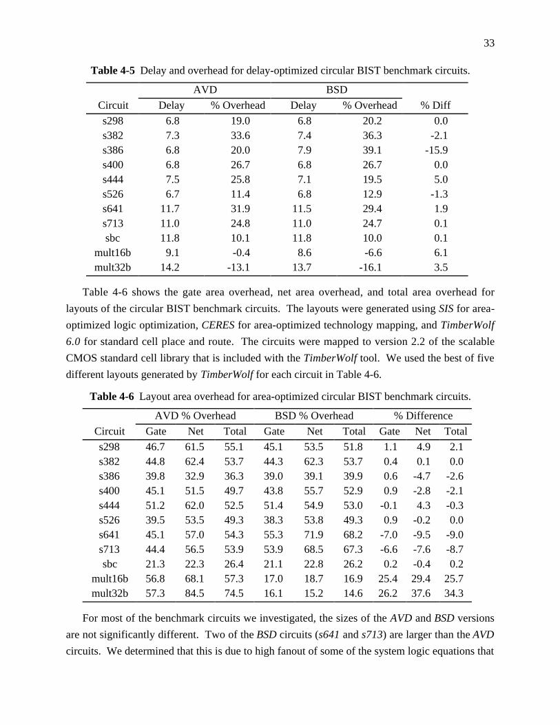
33
Table 4-5 Delay and overhead for delay-optimized circular BIST benchmark circuits.
AVD BSD
Circuit Delay % Overhead Delay % Overhead % Diff
s298 6.8 19.0 6.8 20.2 0.0s382 7.3 33.6 7.4 36.3 -2.1s386 6.8 20.0 7.9 39.1 -15.9s400 6.8 26.7 6.8 26.7 0.0s444 7.5 25.8 7.1 19.5 5.0s526 6.7 11.4 6.8 12.9 -1.3s641 11.7 31.9 11.5 29.4 1.9s713 11.0 24.8 11.0 24.7 0.1sbc 11.8 10.1 11.8 10.0 0.1
mult16b 9.1 -0.4 8.6 -6.6 6.1mult32b 14.2 -13.1 13.7 -16.1 3.5
Table 4-6 shows the gate area overhead, net area overhead, and total area overhead for
layouts of the circular BIST benchmark circuits. The layouts were generated using SIS for area-
optimized logic optimization, CERES for area-optimized technology mapping, and TimberWolf
6.0 for standard cell place and route. The circuits were mapped to version 2.2 of the scalable
CMOS standard cell library that is included with the TimberWolf tool. We used the best of five
different layouts generated by TimberWolf for each circuit in Table 4-6.
Table 4-6 Layout area overhead for area-optimized circular BIST benchmark circuits.
AVD % Overhead BSD % Overhead % Difference
Circuit Gate Net Total Gate Net Total Gate Net Total
s298 46.7 61.5 55.1 45.1 53.5 51.8 1.1 4.9 2.1s382 44.8 62.4 53.7 44.3 62.3 53.7 0.4 0.1 0.0s386 39.8 32.9 36.3 39.0 39.1 39.9 0.6 -4.7 -2.6s400 45.1 51.5 49.7 43.8 55.7 52.9 0.9 -2.8 -2.1s444 51.2 62.0 52.5 51.4 54.9 53.0 -0.1 4.3 -0.3s526 39.5 53.5 49.3 38.3 53.8 49.3 0.9 -0.2 0.0s641 45.1 57.0 54.3 55.3 71.9 68.2 -7.0 -9.5 -9.0s713 44.4 56.5 53.9 53.9 68.5 67.3 -6.6 -7.6 -8.7sbc 21.3 22.3 26.4 21.1 22.8 26.2 0.2 -0.4 0.2
mult16b 56.8 68.1 57.3 17.0 18.7 16.9 25.4 29.4 25.7mult32b 57.3 84.5 74.5 16.1 15.2 14.6 26.2 37.6 34.3
For most of the benchmark circuits we investigated, the sizes of the AVD and BSD versions
are not significantly different. Two of the BSD circuits (s641 and s713) are larger than the AVD
circuits. We determined that this is due to high fanout of some of the system logic equations that
34
are re-structured for beneficial scan dependence in the circular BIST path according to Fig. 4-4.
An enhancement to the synthesis technique should consider the fanout of the system logic when
determining whether or not a particular system logic equation is beneficial for scan dependence.
According to Tables 4-4, 4-5, and 4-6, the BSD versions of two of the circuits (mult16b,
mult32b) have significantly less area and delay than the AVD versions of these circuits. The
reason for this low overhead is that both mult16b and mult32b perform a serial multiplication
operation which has the property that many of the system logic equations are case-3 equations.
Our synthesis technique is able to arrange the bistables into a circular BIST path such that most
of the bistables are case-3 scan dependent on the previous bistable in the path, and these case-3
equations have very little overhead for BIST (see Fig. 4-4c). We focus on this property of
arithmetic operations in the Sec. 5 discussion of scan dependence in data path logic.
4.3.2 Fault Simulation Results
We performed extensive fault simulations on several of the benchmark circuits in order to
evaluate how scan dependence affects the quality of BIST operation. For each benchmark
circuit, we created four different circuit models for gate-level, single stuck-at fault simulation:
FNL, IGN, AVD, and BSD. The FNL version is the original benchmark circuit, and it executes
normal operation during the fault simulation. The front-end test logic shown in Fig. 2-5b was
used for every bistable in the IGN version (IGN stands for ignore scan dependence), and the
bistables were arranged into a circular BIST path such that the number of scan dependent
bistables was maximized. The AVD and BSD circuits were generated as described previously in
this section. The fault simulation results are given in Table 4-7. The fault coverage is the
percentage of collapsed, single stuck-at faults that are detected at least once during BIST
operation, and is a measure of the quality of the TPG operation. We define error loss as the
percentage of clock cycles for which the faulty and fault-free machines are identical (i.e., the
percentage of aliased clock cycles) given that the fault has been detected. Error loss is a measure
of the quality of the ORA operation. Table 4-7 shows that the BSD versions of the benchmark
circuits have the highest fault coverage, and for most of the circuits, the lowest error loss. The
slightly elevated error loss for the BSD version of circuit s386 could be attributed to the fact that
its circular BIST path has three fewer bistables than the AVD version. Even if a circuit has a high
fault coverage percentage, a non-zero error loss percentage means that there is a chance that a
defective circuit will be labeled fault-free even if the fault is detected at some time during the
BIST operation. The defective circuit can only be identified if the BIST operation terminates on
a non-aliased state.
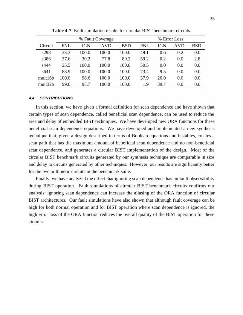
35
Table 4-7 Fault simulation results for circular BIST benchmark circuits.
% Fault Coverage % Error Loss
Circuit FNL IGN AVD BSD FNL IGN AVD BSD
s298 33.3 100.0 100.0 100.0 49.1 0.6 0.2 0.0s386 37.6 30.2 77.8 80.2 59.2 0.2 0.0 2.8s444 35.5 100.0 100.0 100.0 50.5 0.0 0.0 0.0s641 88.9 100.0 100.0 100.0 73.4 9.5 0.0 0.0
mult16b 100.0 98.6 100.0 100.0 37.9 26.0 0.0 0.0mult32b 99.0 95.7 100.0 100.0 1.9 39.7 0.0 0.0
4.4 CONTRIBUTIONS
In this section, we have given a formal definition for scan dependence and have shown that
certain types of scan dependence, called beneficial scan dependence, can be used to reduce the
area and delay of embedded BIST techniques. We have developed new ORA functions for these
beneficial scan dependence equations. We have developed and implemented a new synthesis
technique that, given a design described in terms of Boolean equations and bistables, creates a
scan path that has the maximum amount of beneficial scan dependence and no non-beneficial
scan dependence, and generates a circular BIST implementation of the design. Most of the
circular BIST benchmark circuits generated by our synthesis technique are comparable in size
and delay to circuits generated by other techniques. However, our results are significantly better
for the two arithmetic circuits in the benchmark suite.
Finally, we have analyzed the effect that ignoring scan dependence has on fault observability
during BIST operation. Fault simulations of circular BIST benchmark circuits confirms our
analysis: ignoring scan dependence can increase the aliasing of the ORA function of circular
BIST architectures. Our fault simulations have also shown that although fault coverage can be
high for both normal operation and for BIST operation where scan dependence is ignored, the
high error loss of the ORA function reduces the overall quality of the BIST operation for these
circuits.

36
5 SCAN DEPENDENCE IN DATA PATH LOGIC
The synthesis technique described in Sec. 4 is a general technique for maximizing beneficial
scan dependence given that the system logic is described in terms of Boolean equations and
bistables. One way to maximize beneficial scan dependence in data path logic is to first apply
high-level synthesis operations to a data flow description of the design, then apply the technique
described in Sec. 4 to the generated data path logic. Unfortunately, due to the types of function
blocks typically found in data path logic (e.g., multipliers, adders), generating the dependence
graph for the data path bistables could be very computationally expensive. More importantly,
the high-level synthesis technique may generate data path logic with few beneficial dependencies
between the bistables.
In this section, we describe a method for increasing the beneficial dependencies between
system bistables during high-level synthesis. There are several advantages when beneficial scan
dependence is considered during high-level synthesis of data path logic, where the input to
synthesis is a data flow description, rather than Boolean equations. First, we can simplify the
generation of the dependence graph since the Boolean equations for the system logic can be
inferred for multiple bistables given a single operation in a data flow equation. For example,
given the data flow equation R3 = R1 ADD R2, where R1, R2, and R3 are n-bit registers, we caninfer that the system logic equation for each bistable, Bi, of register R3 has the form R3i = R1i Å
R2i Å Ci, where Ci is the carry function for Bi. We need not perform Shannon decomposition on
the system logic equations of the addition operation in order to determine the dependence
information for the bistables in R3. Second, in data path logic, all bistables in a register are
typically controlled by the same group of control signals. When test operation control signals
can be used in the same manner, i.e., one block of test control logic for each register rather than
for each bistable in the design, test overhead can be reduced. Finally, since the synthesis
technique determines how variables in the data flow description are assigned to bistables, it may
be able to generate data path logic with more instances of case-1, case-2, and case-3
dependencies between the bistables, resulting in a lower-cost, self-testable design.
This section is a summary of the material in [Avra 92] and Sec. 6 of [Avra 94a] and contains
a discussion of how to apply the synthesis technique described in Sec. 4 to data path logic. We
first describe a new scan path architecture for data path logic, called orthogonal scan path, where
the shift direction in the orthogonal scan path is orthogonal to the shift direction in traditional
scan paths (shifting bits within registers). We then identify data path functions that are well-
suited for the synthesis technique described in Sec. 4, and show that the occurrence of these
functions can be increased if an orthogonal scan path is used in the data path logic. Finally, we
discuss a register binding technique that, assuming an orthogonal scan path architecture, attempts
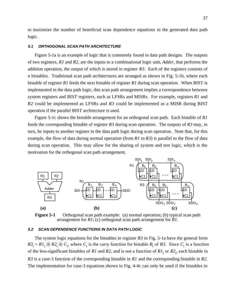
37
to maximize the number of beneficial scan dependence equations in the generated data path
logic.
5.1 ORTHOGONAL SCAN PATH ARCHITECTURE
Figure 5-1a is an example of logic that is commonly found in data path designs. The outputs
of two registers, R1 and R2, are the inputs to a combinational logic unit, Adder, that performs the
addition operation, the output of which is stored in register R3. Each of the registers consists of
n bistables. Traditional scan path architectures are arranged as shown in Fig. 5-1b, where each
bistable of register R1 feeds the next bistable of register R1 during scan operation. When BIST is
implemented in the data path logic, this scan path arrangement implies a correspondence between
system registers and BIST registers, such as LFSRs and MISRs. For example, registers R1 and
R2 could be implemented as LFSRs and R3 could be implemented as a MISR during BIST
operation if the parallel BIST architecture is used.
Figure 5-1c shows the bistable arrangement for an orthogonal scan path. Each bistable of R1
feeds the corresponding bistable of register R3 during scan operation. The outputs of R3 may, in
turn, be inputs to another register in the data path logic during scan operation. Note that, for this
example, the flow of data during normal operation (from R1 to R3) is parallel to the flow of data
during scan operation. This may allow for the sharing of system and test logic, which is the
motivation for the orthogonal scan path arrangement.
R1 R2
R3
Adder 1D
C1
1D
C1
1D
C1
1D
C1
1D
C1
1D
C1
1D
C1
1D
C1
1D
C1
R11
SDI
2 n
SDO
SDI
R1
R3B B B
1 2 nB B B
1 2 nB B B
1 SDI2 SDIn
SDO1 SDO2 SDOn
(a) (b) (c)
Figure 5-1 Orthogonal scan path example: (a) normal operation; (b) typical scan patharrangement for R1; (c) orthogonal scan path arrangement for R1.
5.2 SCAN DEPENDENCE FUNCTIONS IN DATA PATH LOGIC
The system logic equations for the bistables in register R3 in Fig. 5-1a have the general formR3i = R1i Å R2i Å Ci, where Ci is the carry function for bistable Bi of R3. Since Ci is a function
of the less-significant bistables of R1 and R2, and is not a function of R1i or R2i, each bistable in
R3 is a case-3 function of the corresponding bistable in R1 and the corresponding bistable in R2.
The implementation for case-3 equations shown in Fig. 4-4c can only be used if the bistables in

38
either R1 or R2 immediately precede the corresponding bistables in R3 in the scan path. This can
be accomplished when an orthogonal scan path is used in the data path logic.
Table 5-1 lists seven types of system logic equations for bistables in data path logic that we
have determined can benefit from scan dependence. The equation type and an associated area
overhead cost estimate based on LSI Logic cell units [LSI 91] are listed, where n represents the
width of the data path (i.e., the number of bistables in each register). Lower-case letters a and b
represent system logic control signals that determine the input to each bistable of register R1.
Upper-case letters F and G represent outputs of combinational logic, the inputs to which are
primary inputs and outputs of bistables excluding the corresponding bistables associated with
register R2. For example, for a 2-bit data path (n = 2), the equation R1 = a' R2 + a F represents
two system logic equations:
Z10 = a' Q20 + a F0Z11 = a' Q21 + a F1
where F0 is not a function of Q20, and F1 is not a function of Q21.
Table 5-1 System equations for data path registers that benefit from scan dependence.
Type Cost Function
1 0 R1 = R22 4 R1 = a' R2 + a (R2 Å F)
3 4n R1 = R2 Å F
4 12+2n R1 = a' b' R2 + a' b (R2 Å F) + a G
5 4+8n R1 = a' (R2 Å F) + a G6 8+8n R1 = a' R2 + a F7 10n R1 = R2 + F8 18n R1 = F
Data flow equation types 1, 7, and 3 correspond to the case-1, case-2, and case-3 equations,
respectively, described in Sec. 4.2, and the bistables of these registers can be implemented as
shown in Fig. 4-4. Equation types 2, 4, 5, and 6 are combinations of case-1 and case-3 equations
and have control logic can be shared between the test control signals and system control signals a
and b. If the system logic equation for R1 cannot be classified as one of the first seven types of
equations shown in Table 5-1, it is classified as type 8, and the more general synthesis technique
described in Sec. 4 can be applied to determine whether or not beneficial scan dependence exists
for any of the bistables in the register. Register R3 in Fig. 5-1a can be represented by the type-3
equation in Table 5-1, R1 = R2 Å F.
We have identified two types of operations that are common in data path designs and can be
mapped to equation types 1-6 in Table 5-1: addition operations and live variable motion.
Addition operations are common in DSP-based data path designs. [Waser 82] describes several

39
types of adder implementations, including conditional sum, Ling, and carry-look-ahead adders.The output equations for each of these adder implementations can be expressed as: R1i = R2i Å
R3i Å Ci, where Ci is a function of the less-significant bistables of R2 and R3, and is not a
function of R2i or R3i. The logic implementation for Ci varies with adder type. If any of the
variables in the data flow description that are assigned to register R1 are the result of an addition
operation, it may be possible to implement R1 by one of equation types 2-5 in Table 5-1.
Another type of function that can occur in data path designs is the transfer of data from one
register to the next, known as live variable motion. Variables whose lifetimes are longer than
one clock cycle can either be held in a single register, or transferred from one register to another.
When the latter technique is used, equations of the form R1 = a R2 + a' F occur in the data path
logic, where a live variable is transferred from R2 to R1 whenever control signal a = 1.
Depending on the logic that generates F, this equation can be mapped to equation types 1, 2, 4, 5,
6, or 7 in Table 5-1. Figure 5-2a is a data flow graph illustrating live variable motion. Variable
H is loaded into register R3 during the first clock cycle, but is not needed for computation until
the second clock cycle, and so is loaded into R2 during the second clock cycle. Variable G is
loaded into R2 during the first clock cycle. The system logic equations for the bistables of R2 are
type-6 equations, which can be implemented as shown in Fig. 5-2b. The control signal a is high
during the first clock cycle and low during the second. The test logic overhead for this case
consists of two AND gates per bistable in R2 plus an AND gate and an OR gate to generate
control signals for all bistables in the register. The exclusive-OR gate is used to perform the
MISR function during BIST operation and a multiplexer function during normal operation.
5.3 RESULTS
Our high-level synthesis procedure for beneficial scan dependence assumes that the data path
logic has an orthogonal scan path architecture, and biases the register binding operation to assign
variables in the data flow equations to registers such that equation types 1-7 listed in Table 5-1
are used most often. This synthesis procedure was applied to two high-level synthesis
benchmark circuits, Tseng [Tseng 86] and DiffEq [Paulin 89a]. The results are presented in
Table 5-2. The size of the data path (in LSI Logic cell units [LSI 91]) and the overhead for test
logic as a percentage of total size are given for two situations: 1) bistables are arranged into
orthogonal scan paths after register binding (labeled “Test Synthesis”), and 2) equation types 1-7
in Table 5-1 are favored during register binding (labeled “Synthesis-for-Test”). We assumed a
16-bit data path, and estimated interconnect area as being one cell unit per interconnection. For
both the test synthesis and synthesis-for-test procedures, beneficial scan dependence was
maximized by using an orthogonal scan path arrangement in a circular BIST architecture. For

40
both examples, the total size and the test overhead are smaller when scan dependence is
considered during register binding.
T &Å 1D
C1
R3
R2
Test Overhead
&
&
+
G
T
aa'
R1 R3R2
R2R1
R1
F G H
+
+
to each bistable in R2
1
2
i
i i
(a) (b)
Figure 5-2 Live variable motion: (a) data flow graph; (b) implementation of bistables in R2.
Table 5-2 Data path design examples with orthogonal scan path and circular BIST.
Test Synthesis Synthesis-for-Test
Design Size (cell units) % Overhead Size (cell units) % Overhead
Tseng 14,146 13.5 11,574 6.4DiffEq 12,342 11.7 11,518 7.3
5.4 CONTRIBUTIONS
We have developed a new scan path architecture for data path logic called orthogonal scan
path. The motivation for using this type of scan path arrangement is that it can increase the
number of beneficial dependencies between the bistables in the data path logic, which allows for
more sharing of system and test logic. We have identified seven types of data path equations that
are beneficial for scan dependence, and have shown that using an orthogonal scan path increases
the occurrence of these types of equations. We discussed the synthesis of two data path design
examples and showed that, when the register binding operation assumes an orthogonal scan path
and is biased toward generating data path logic with certain structures for addition operations and
live variable motion, lower-cost circular BIST designs result.

41
6 SYNTHESIS-FOR-TEST DESIGN SYSTEM
In this section, we describe a computer-aided design system, named Odin, that automatically
generates a synchronous hardware design given a behavioral, VHDL description of the design.
Existing hardware synthesis systems typically use cost and performance as the main criteria to be
satisfied when generating a design from a behavioral description, and seldom even consider test
issues during the synthesis process. The purpose of Odin is to serve as a platform for the
development of synthesis techniques that generate low-cost, high-performance hardware
implementations that also meet specified testability requirements. By considering testability
during the synthesis process, Odin is able to generate designs that are optimized for specific test
techniques. Odin can currently generate designs optimized for both parallel and circular BIST
architectures.
We have implemented in Odin all of the major design system algorithms necessary for the
generation of data path and control logic given a behavioral VHDL description: VHDL input
and output file processing algorithms, internal data structure creation and manipulation
algorithms, and high-level synthesis algorithms. Emphasis was placed on ease of modification
when implementing the system in order to encourage the addition of future synthesis-for-test
techniques. In this section, we describe the current capabilities of Odin. A more detailed
description is given in [Avra 94b]. Section 6.1 is a brief overview of the Odin design system.
Section 6.2 describes the VHDL input and output files for the design system: the input
behavioral description, the component library that Odin accesses when performing synthesis
operations, and the output structural description. Section 6.3 contains a description of the
hierarchical data and control flow graph that is Odin’s major internal data structure. Finally, in
Sec. 6.4, we describe the high-level synthesis operations that are currently implemented in Odin.
6.1 OVERVIEW
Figure 6-1 illustrates the flow of tasks that are performed by the Odin design system. The
input to Odin is a VHDL intermediate format (VIF) description that represents the behavioral
description of the design. A commercial VHDL compiler, developed by Vantage Analysis
Systems, is used to create VIF from the input behavioral description. Several transformations are
applied to the VIF description in order to simplify Odin’s internal data structures. VIF access
routines supplied by Vantage are used to transform the VIF description into a data and control
flow graph (DCFG). Compiler optimizations are applied to the DCFG in order to minimize the
amount of code that must be mapped to hardware. If the behavioral VHDL description contains
multiple process statements, inter-process communication can be analyzed [Martinolle 91] in
order to extract all potential functional parallelism in the description so that the most efficient

42
hardware can be synthesized. The first task in high-level synthesis is scheduling, where
operations (e.g., addition, comparison, multiplication) in the behavioral description are assigned
to specific clock cycles based upon data dependencies and the delays of the hardware
components that are used to implement the operations. Operations and variables are then
mapped to hardware components from a user-specified VHDL component library. Control logic
that generates control signals for the components in the data path logic is synthesized based upon
the selected schedule and the binding of operations and variables to hardware components. The
output is structural VHDL descriptions of control logic and data path logic that implement the
input behavioral description.
- Process Statements- Signal Assignments
- Constant Propagation- Loop Unrolling- Dead Code Elmination
- Resolve Signal Assignments- Maximize Parallelism
- Scheduling- Operator Allocation and Binding- Register Allocation and Binding- Control logic generation
Data Path Logic
VHDLTransformations
Compiler Optimizations
Interprocess Analysis
High-Level Synthesis
DCFG Creation
Control Logic
VantageVHDL Compiler
ComponentLibrary
BehavioralModel
VIF
Structural VHDL
Figure 6-1 Odin design system overview.
6.2 DESIGN SYSTEM INPUT AND OUTPUT
As shown in Fig. 6-1, the input to Odin consists of two VIF data structures, generated by the
Vantage compiler from VHDL source code. The data structures represent a behavioral model of
the design and a library of hardware components used by the synthesis techniques to generate a
structural implementation.
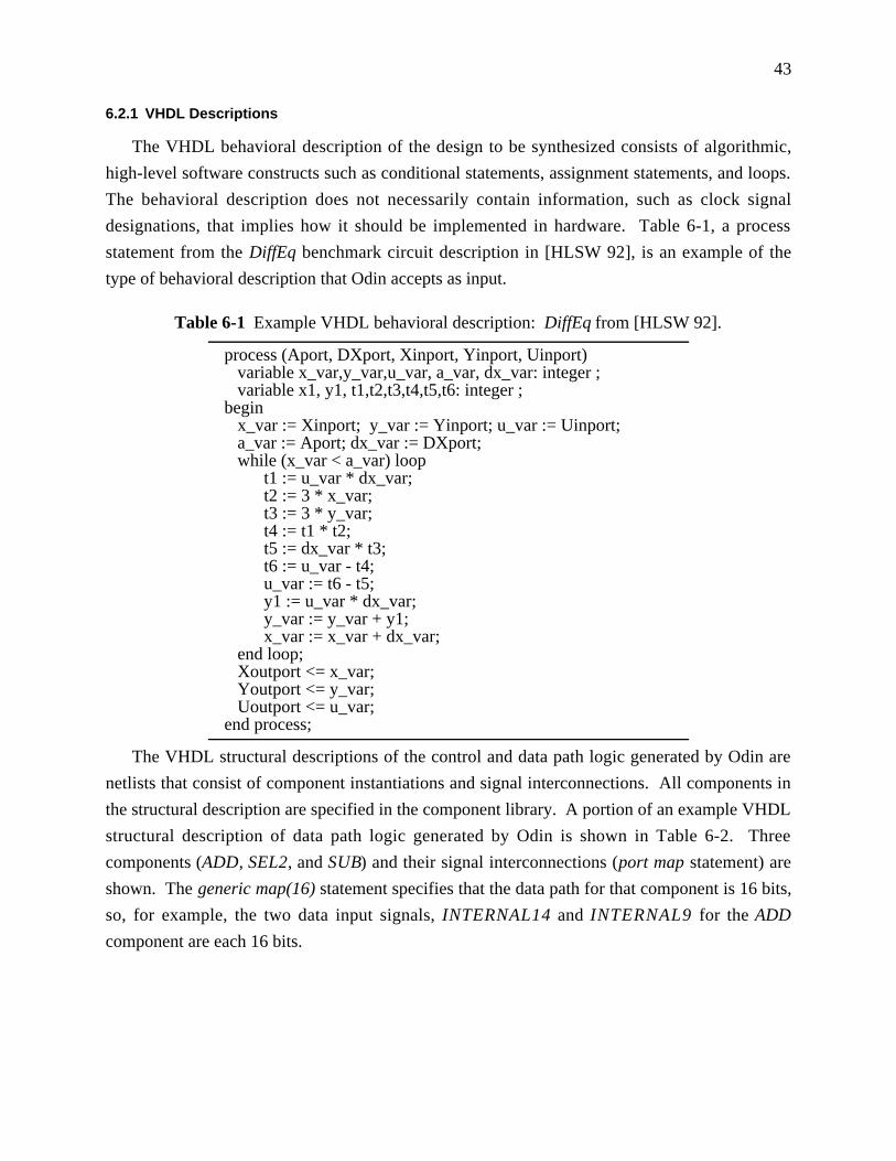
43
6.2.1 VHDL Descriptions
The VHDL behavioral description of the design to be synthesized consists of algorithmic,
high-level software constructs such as conditional statements, assignment statements, and loops.
The behavioral description does not necessarily contain information, such as clock signal
designations, that implies how it should be implemented in hardware. Table 6-1, a process
statement from the DiffEq benchmark circuit description in [HLSW 92], is an example of the
type of behavioral description that Odin accepts as input.
Table 6-1 Example VHDL behavioral description: DiffEq from [HLSW 92].
process (Aport, DXport, Xinport, Yinport, Uinport)variable x_var,y_var,u_var, a_var, dx_var: integer ;variable x1, y1, t1,t2,t3,t4,t5,t6: integer ;
beginx_var := Xinport; y_var := Yinport; u_var := Uinport;a_var := Aport; dx_var := DXport;while (x_var < a_var) loop
t1 := u_var * dx_var;t2 := 3 * x_var;t3 := 3 * y_var;t4 := t1 * t2;t5 := dx_var * t3;t6 := u_var - t4;u_var := t6 - t5;y1 := u_var * dx_var;y_var := y_var + y1;x_var := x_var + dx_var;
end loop;Xoutport <= x_var;Youtport <= y_var;Uoutport <= u_var;
end process;
The VHDL structural descriptions of the control and data path logic generated by Odin are
netlists that consist of component instantiations and signal interconnections. All components in
the structural description are specified in the component library. A portion of an example VHDL
structural description of data path logic generated by Odin is shown in Table 6-2. Three
components (ADD, SEL2, and SUB) and their signal interconnections (port map statement) are
shown. The generic map(16) statement specifies that the data path for that component is 16 bits,
so, for example, the two data input signals, INTERNAL14 and INTERNAL9 for the ADD
component are each 16 bits.
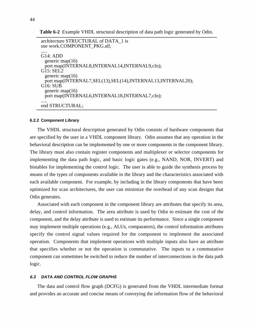
44
Table 6-2 Example VHDL structural description of data path logic generated by Odin.
architecture STRUCTURAL of DATA_1 isuse work.COMPONENT_PKG.all;.....G14: ADD
generic map(16)port map(INTERNAL8,INTERNAL14,INTERNAL9,cIn);
G15: SEL2generic map(16)port map(INTERNAL7,SEL(13),SEL(14),INTERNAL13,INTERNAL20);
G16: SUBgeneric map(16)port map(INTERNAL6,INTERNAL18,INTERNAL7,cIn);
.....end STRUCTURAL;
6.2.2 Component Library
The VHDL structural description generated by Odin consists of hardware components that
are specified by the user in a VHDL component library. Odin assumes that any operation in the
behavioral description can be implemented by one or more components in the component library.
The library must also contain register components and multiplexer or selector components for
implementing the data path logic, and basic logic gates (e.g., NAND, NOR, INVERT) and
bistables for implementing the control logic. The user is able to guide the synthesis process by
means of the types of components available in the library and the characteristics associated with
each available component. For example, by including in the library components that have been
optimized for scan architectures, the user can minimize the overhead of any scan designs that
Odin generates.
Associated with each component in the component library are attributes that specify its area,
delay, and control information. The area attribute is used by Odin to estimate the cost of the
component, and the delay attribute is used to estimate its performance. Since a single component
may implement multiple operations (e.g., ALUs, comparators), the control information attributes
specify the control signal values required for the component to implement the associated
operation. Components that implement operations with multiple inputs also have an attribute
that specifies whether or not the operation is commutative. The inputs to a commutative
component can sometimes be switched to reduce the number of interconnections in the data path
logic.
6.3 DATA AND CONTROL FLOW GRAPHS
The data and control flow graph (DCFG) is generated from the VHDL intermediate format
and provides an accurate and concise means of conveying the information flow of the behavioral

45
description to the compiler optimization and synthesis operations. The DCFG has two levels of
hierarchy. The top level is created by partitioning the behavioral description into basic blocks
and control statements. A basic block is a sequence of consecutive assignment statements from
the behavioral description. Figure 6-2a shows an example VHDL behavioral description that is
partitioned into two control statements (circled), a wait and an if, and two basic blocks. The
DCFG has six different types of nodes: Wait, If, and Case, which correspond to wait, if, and case
statements, respectively, While for loop statements, EndCond for joining the mutually-exclusive
branches of conditional statements, and BB for basic blocks. The information associated with
each node depends upon its type. For example, Wait nodes are numbered since there are
typically multiple wait statements in a VHDL behavioral description. Each Wait node also has a
pointer to the list of signals to which the corresponding wait statement is sensitive. Figure 6-2b
shows the top level of the DCFG for the process statement given in Fig. 6-2a. The five nodes are
labeled N1 - N5. Edges in the DCFG represent the branching of operation between the behavioral
statements represented by the nodes. A value associated with an edge represents the condition
under which that branch is taken.
Processvariable a, b: integer;
Beginwait unil go = '1';if (y > x + 3) then
b := a + 1;a := y + 1;x <= a*b;
elseb := a + 2;a := y + 2;x <= b;
end if;End Process;
Wait
If
go = '1'
y > x + 3
b := a + 1;a := y + 1;x <= a*b;
BBb := a + 2;a := y + 2;x <= b;
BBfalse true
true
false
EndCond
N1
N2
N3 N4
N5
(a) (b)
Figure 6-2 DCFG example: (a) partitioned behavioral description; (b) top level of theDCFG.
A data flow graph (DFG) is associated with each node in the DCFG except for EndCond
nodes. The data flow graph is a directed, acyclic graph that specifies the operations and the data
dependencies of a basic block or an expression. Each node in the DFG represents an operation in
the behavioral description. A directed edge from node Ni to node Nj specifies that the output of
the operation represented by node Ni is an input to the operation represented by node Nj. Each

46
DFG has a source node (SRC) which only has outgoing edges that represent variables that are
outputs of other DFGs, and a sink node (SNK) which only has incoming edges that represent
variables that are inputs of other DFGs. The DFG for basic block nodes specifies how the
variables defined by the statements in the basic block (a variable is defined if it appears on the
left-hand-side of an assignment statement) are used in subsequent statements of the block (see
Fig. 6-3a). The DFG for control nodes (Wait, For, While, If, Case) represents the conditional
expression associated with the control statement. For example, the DFG associated with an If
node represents the conditional expression of the If statement (see Fig. 6-3b).
+
SRC
b := a + 1;a := y + 1;x <= a*b;
BB
+
x
SNK
a1 y 1
x a
b a
Ify > x + 3
SRC
SNK
+
>
x
3y
(a) (b)
Figure 6-3 Data flow graphs: (a) BB node DFG; (b) If node DFG.
Odin uses the DCFG to perform several basic compiler optimizations on the input behavioral
description in order to minimize the amount of code that must be mapped to hardware and to
improve the performance of the final design. The first optimization performed is constant
propagation, where each use of a constant is replaced with its value. This simplifies expressions
in the behavioral description and reduces the cost of the hardware that implements those
expressions. For example, the expression x=y can be implemented in hardware with n exclusive-
NOR gates and one n-input AND gate, where x is an n-bit variable, and y is an n-bit constant
with value 17. When constant propagation is applied, the resulting expression, x=17, can be
implemented with just one n-input AND gate. Next, Odin analyzes the flow of data in the DFGs
in order to identify dead code (statements that can be removed without affecting the behavior of
the description) that can be eliminated from the behavioral description. Since dead code does not
contribute to the behavior of the design, Odin removes it before synthesis so that it is not mapped
to hardware. Dead code may result from previously-applied compiler optimizations, such as
constant propagation, or may be inadvertently introduced by the designer. The final optimization
applied to the DCFG is to unroll loops with definite limits, where the limits do not exceed a
specified maximum. The statements within a loop are executed sequentially for each iteration of
the loop. When the data dependencies between the statements within the loop are such that they
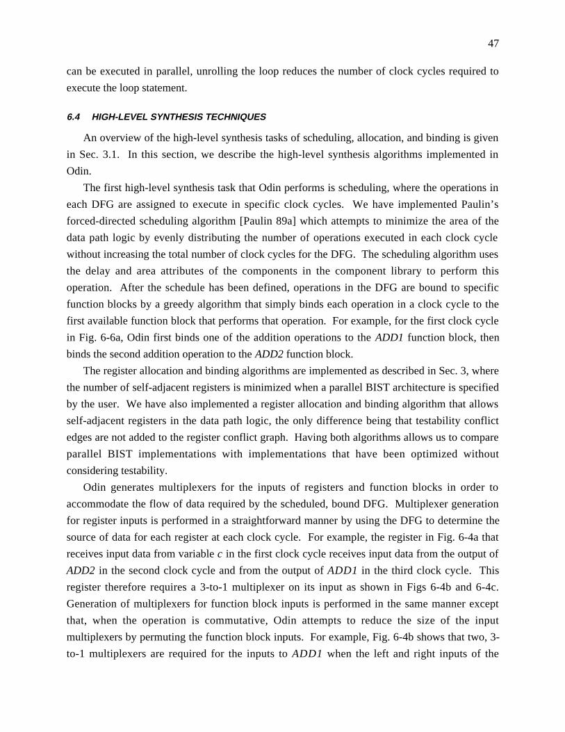
47
can be executed in parallel, unrolling the loop reduces the number of clock cycles required to
execute the loop statement.
6.4 HIGH-LEVEL SYNTHESIS TECHNIQUES
An overview of the high-level synthesis tasks of scheduling, allocation, and binding is given
in Sec. 3.1. In this section, we describe the high-level synthesis algorithms implemented in
Odin.
The first high-level synthesis task that Odin performs is scheduling, where the operations in
each DFG are assigned to execute in specific clock cycles. We have implemented Paulin’s
forced-directed scheduling algorithm [Paulin 89a] which attempts to minimize the area of the
data path logic by evenly distributing the number of operations executed in each clock cycle
without increasing the total number of clock cycles for the DFG. The scheduling algorithm uses
the delay and area attributes of the components in the component library to perform this
operation. After the schedule has been defined, operations in the DFG are bound to specific
function blocks by a greedy algorithm that simply binds each operation in a clock cycle to the
first available function block that performs that operation. For example, for the first clock cycle
in Fig. 6-6a, Odin first binds one of the addition operations to the ADD1 function block, then
binds the second addition operation to the ADD2 function block.
The register allocation and binding algorithms are implemented as described in Sec. 3, where
the number of self-adjacent registers is minimized when a parallel BIST architecture is specified
by the user. We have also implemented a register allocation and binding algorithm that allows
self-adjacent registers in the data path logic, the only difference being that testability conflict
edges are not added to the register conflict graph. Having both algorithms allows us to compare
parallel BIST implementations with implementations that have been optimized without
considering testability.
Odin generates multiplexers for the inputs of registers and function blocks in order to
accommodate the flow of data required by the scheduled, bound DFG. Multiplexer generation
for register inputs is performed in a straightforward manner by using the DFG to determine the
source of data for each register at each clock cycle. For example, the register in Fig. 6-4a that
receives input data from variable c in the first clock cycle receives input data from the output of
ADD2 in the second clock cycle and from the output of ADD1 in the third clock cycle. This
register therefore requires a 3-to-1 multiplexer on its input as shown in Figs 6-4b and 6-4c.
Generation of multiplexers for function block inputs is performed in the same manner except
that, when the operation is commutative, Odin attempts to reduce the size of the input
multiplexers by permuting the function block inputs. For example, Fig. 6-4b shows that two, 3-
to-1 multiplexers are required for the inputs to ADD1 when the left and right inputs of the
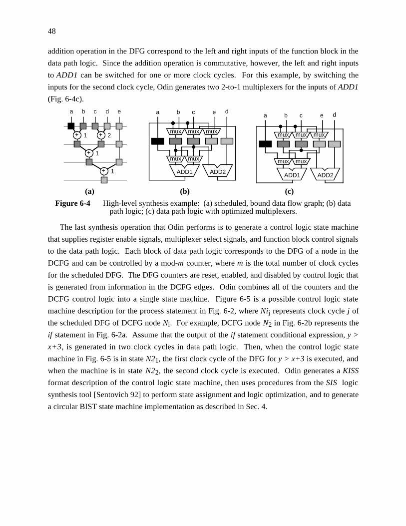
48
addition operation in the DFG correspond to the left and right inputs of the function block in the
data path logic. Since the addition operation is commutative, however, the left and right inputs
to ADD1 can be switched for one or more clock cycles. For this example, by switching the
inputs for the second clock cycle, Odin generates two 2-to-1 multiplexers for the inputs of ADD1
(Fig. 6-4c).
ADD1
mux
a b a b c e
mux
+
+
c d
mux mux
mux+ +
e
ADD2
d
ADD1
mux
a b c e
mux
mux mux
mux
ADD2
d
1
1
1
2
(a) (b) (c)
Figure 6-4 High-level synthesis example: (a) scheduled, bound data flow graph; (b) datapath logic; (c) data path logic with optimized multiplexers.
The last synthesis operation that Odin performs is to generate a control logic state machine
that supplies register enable signals, multiplexer select signals, and function block control signals
to the data path logic. Each block of data path logic corresponds to the DFG of a node in the
DCFG and can be controlled by a mod-m counter, where m is the total number of clock cycles
for the scheduled DFG. The DFG counters are reset, enabled, and disabled by control logic that
is generated from information in the DCFG edges. Odin combines all of the counters and the
DCFG control logic into a single state machine. Figure 6-5 is a possible control logic state
machine description for the process statement in Fig. 6-2, where Nij represents clock cycle j of
the scheduled DFG of DCFG node Ni. For example, DCFG node N2 in Fig. 6-2b represents the
if statement in Fig. 6-2a. Assume that the output of the if statement conditional expression, y >
x+3, is generated in two clock cycles in data path logic. Then, when the control logic state
machine in Fig. 6-5 is in state N21, the first clock cycle of the DFG for y > x+3 is executed, and
when the machine is in state N22, the second clock cycle is executed. Odin generates a KISS
format description of the control logic state machine, then uses procedures from the SIS logic
synthesis tool [Sentovich 92] to perform state assignment and logic optimization, and to generate
a circular BIST state machine implementation as described in Sec. 4.

49
N11 N21 N22
N41 N42
N31 N32y > x + 3
y £ x + 3
go = 1go ¹ 1
Figure 6-5 Control logic state machine description for Fig. 6-2.

50
7 CONCLUDING REMARKS
In this dissertation, we have described new synthesis techniques that generate built-in self-
testable designs. The primary objective of these synthesis-for-BIST techniques is to satisfy
requirements associated with a specific BIST architecture when generating the system logic
structural implementation. Cost is minimized and performance is maximized to the extent that
BIST requirements are not compromised. Considering BIST issues during system logic
synthesis allows for the generation of system logic that is optimized for a particular BIST
architecture and that can be more effectively tested by the BIST operation.
In particular, we investigated techniques for generating low-cost, built-in self-testable designs
that are free of the types of system bistable dependencies that can reduce the effectiveness of the
embedded MISRs that are used to perform BIST operations. We showed that some types of
system bistable dependencies can reduce the effectiveness of BIST, whereas other types of
dependencies can allow sharing of BIST and scan logic with system logic, thereby reducing
BIST overhead. Care must be taken, however, when system logic and BIST logic is shared, so
that the BIST operation effectiveness is not compromised.
Our first synthesis technique, allocation and binding for parallel BIST (Sec. 3), minimizes the
number of self-adjacent registers in the generated design without increasing the latency of the
design. We have implemented the technique in our synthesis-for test design tool, and results
show that, for the examples investigated, our technique generates the lowest-cost parallel BIST
implementation and generates system logic that is comparable in cost to techniques that do not
consider BIST during synthesis. There is one situation for which the generation of a self-
adjacent register is unavoidable without changing the schedule or operation binding of the input
data flow description. For this case, we use a CBILBO register, which breaks the self-adjacency
during BIST operation. CBILBOs have a higher cost than regular BILBO registers, but have the
advantage that they simultaneously perform the TPG and ORA operations. This can allow for a
reduction in the number of test sessions required for BIST operation. The scheduling and
operation binding techniques could be modified in order to minimize the number of unavoidable
self-adjacencies encountered during register binding, and this is the subject of further research.
In Sec. 2, we showed that generating an ideal parallel BIST architecture requires addressing
complex implementation details such as TPG interconnections, multiple feedback logic blocks,
and test session scheduling. The synthesis technique described in Sec. 3 addresses only one of
these implementation details: self-adjacent registers. One advantage of the ideal parallel BIST
architecture is that the assumptions made in the generation of theoretical results for TPG fault
coverage [Kim 88] and ORA aliasing [Daehn 90] characteristics are applicable, and these results
can be used to estimate the test transparency of the BIST operation. Unfortunately, the

51
remaining implementation complexities must be addressed by synthesis techniques before
automatic generation of an ideal parallel BIST architecture is feasible. It may be necessary for
these techniques to consider more general system bistable (rather than system register)
dependencies during high-level synthesis.
The synthesis techniques described in Secs. 4 and 5 address the more general problem of
system bistable dependency during logic synthesis (Sec. 4) and high-level synthesis (Sec. 5).
Both techniques attempt to maximize sharing of system logic and test logic to reduce the cost
and improve the performance without increasing the test transparency of BIST architectures,
such as circular BIST and parallel BIST, that make use of embedded MISRs. We have
implemented the logic synthesis technique described in Sec. 4 in our system design tool and used
it to generate circular BIST implementations of several sequential logic synthesis benchmark
circuits. For most of the benchmark circuits we investigated, the sizes of the circuits generated
by our technique did not differ significantly from the sizes of circuits with no scan dependence.
However, better results for our technique should be possible when higher-level synthesis
operations, such as state assignment and register binding, are biased toward generating more
system bistables with beneficial dependence equations. Results presented in Sec. 5 showed that
this is true for the register binding operation when an orthogonal scan path configuration is used.
The orthogonal scan path allows for greater sharing of BIST logic and commonly-used data path
logic such as multiplexers and adders.
While the synthesis technique described in Sec. 4 is applicable to any BIST architecture that
uses embedded MISRs, our implementation of the technique generates circular BIST designs
because circular BIST has far fewer complex implementation issues than the parallel BIST
architecture. Unfortunately, theoretical results for TPG fault coverage and ORA aliasing are not
valid for circular BIST because of the dependence of the MISR inputs on the state of the MISR.
Extensive fault simulations of the circular BIST implementation must therefore be executed to
guarantee high-quality BIST operation. Fault simulations of the designs generated by our
synthesis technique show that the test transparency is comparable to circular BIST architectures
that allow no scan dependence. These simulations also showed that for two common design
practices, not including any BIST circuitry, or if circular BIST is implemented, ignoring scan
dependence, fault coverage can be high, but high error loss reduces the overall quality of the
BIST operation. This suggests that further investigation into techniques for improving the ORA
characteristics of self-adjacent MISRs could yield lower-cost, self-testable designs.
52
REFERENCES
[Abadir 85] Abadir, M. S., and M. A. Breuer, “A Knowledge-Based System for Designing
Testable VLSI Chips,” IEEE Des. and Test of Comput., pp. 56-68, August 1985.
[Abramovici 90] Abramovici, M., M. A. Breuer, and A. D. Friedman, Digital Systems Testing
and Testable Design, Computer Science Press, New York, NY, USA 1990.
[ACM 91] ACM/SIGDA 1991 Logic Synthesis Benchmark Circuits, available via anonymous
ftp from mcnc.mcnc.org.
[Avra 90] Avra, L., and E. J. McCluskey, “Behavioral Synthesis of Testable Systems with
VHDL,” Dig. COMPCON Spring 90, San Francisco, pp. 410-415, February 26-March 2, 1990.
[Avra 91] Avra, L., “Allocation and Assignment in High-Level Synthesis for Self-Testable Data
Paths,” Int. Test Conf., Nashville, TN, USA, pp. 463-472, October 26-30, 1991.
[Avra 92] Avra, L., “Orthogonal Built-In Self-Test,” COMPCON Spring 1992 Dig. of Papers,
San Francisco, CA, USA, pp. 452-457, February 24-28, 1992.
[Avra 93] Avra, L. J., and E. J. McCluskey, “Synthesizing for Scan Dependence in Built-In Self-
Testable Designs,” Int. Test Conf., Baltimore, MD, USA, pp. 734-743, October 17-21, 1993.
[Avra 94a] Avra, L. J., and E. J. McCluskey, “Synthesizing for Scan Dependence in Built-In
Self-Testable Designs,” Center for Reliable Comput. Tech. Rpt. 94-2, Comput. Sys. Lab., CSL
TR 94-621, Stanford University, Stanford, CA, May 1994.
[Avra 94b] Avra, L. J., L. Gerboux, J.-C. Giomi, F. Martinolle, and E. J. McCluskey, “A
Synthesis-for-Test Design System,” Center for Reliable Comput. Tech. Rpt. 94-3, Comput.
Sys. Lab., CSL TR 94-622, Stanford University, Stanford, CA, May 1994.
[Bardell 82] Bardell, P. H., and W. H. McAnney, “Self-Testing of Multichip Logic Modules,”
Int. Test Conf., pp. 200-204, November 1982.
[Bardell 87] Bardell, P. H., W. H. McAnney, and J. Savir, Built-In Test for VLSI: Pseudorandom
Techniques, John Wiley & Sons, Inc., 1987.
[Bardell 91] Bardell, P. H., and M. J. Lapointe, “Production Experience with Built-In Self-Test
in the IBM ES/9000 System,” Int. Test Conf. Proc., Nashville, TN, USA, pp. 28-36, October
26-30, 1991.
[Bhatia 93] Bhatia, S. and N. K. Jha, “Synthesis of Sequential Circuits for Robust Path Delay
Fault Testability,” 6th Int. Conf. on VLSI Des., pp. 275-280, January 1993.
[Bonnenberg 93] Bonnenberg, H, A. Curiger, N. Felber, H. Kaeslin, R. Zimmermann, and W.
Fichtner, “VINCI: Secure Test of a VLSI High-Speed Encryption System,” Int. Test Conf.,
Baltimore, MD, USA, pp. 782-790, October 17-21, 1993.

53
[Brayton 87] Brayton, R. K., R. Rudell, A. Sangiovanni-Vincentelli, and A. R. Wang, “MIS: A
Multiple-Level Logic Optimization System,” IEEE Trans. on Comput.-Aided Des., Vol. CAD-
6, No. 6, pp. 1062-1081, November 1987.
[Broseghini 93] Broseghini, J., and D. H. Lenhert, “An ALU-Based Programmable
MISR/Psedudorandom Generator for a MC68HC11 Family Self-Test,” Int. Test Conf.,
Baltimore, MD, USA, pp. 349-358, October 17-21, 1993.
[Bryan 89] Bryan, D., F. Brglez, and R. Lisanke, "Redundancy Identification and Removal," Int.
Workshop on Logic Synthesis, Research Triangle Park, NC, May 23-26, 1989.
[Cheng 89] Cheng, K. T., and V. D. Agrawal, “An Economical Scan Design for Sequential Logic
Test Generation,” Int. Symp. Fault-Tolerant Comput., Chicago, IL, USA, pp. 28-35, June 21-
23, 1989.
[Daehn 90] Daehn, W., T. W. Williams, and K. D. Wagner, “Aliasing Errors in Linear Automata
Used as Multiple-Input Signature Analyzers,” IBM J. Res. Develop., Vol. 34, No. 2/3, pp. 363-
380, March/May 1990.
[De Micheli 94] De Micheli, Giovanni, “Synthesis and Optimization of Digital Circuits,”
McGraw-Hill, Inc., Hightstown, NJ, USA, 1994.
[Devadas 90] Devadas, S., and K. Keutzer, "Synthesis and Optimization Procedures for Robustly
Delay-Fault Testable Combinational Logic Circuits," 27th Des. Autom. Conf., Orlando, FL, pp.
221-227, June 24-29, 1990.
[Frieze 88] Frieze, A. M., “An Algorithm for Finding Hamiltonian Cycles in Random
Directed Graphs,” J. of Algorithms, pp. 181-204, June 1988.
[Gage 93] Gage, R., “Structured CBIST in ASICs,” Int. Test Conf., Baltimore, MD, USA, pp.
332-338, October 17-21, 1993.
[Gelsinger 86] Gelsinger, P. P., “Built In Self Test of the 80386,” Int. Conf. Comput. Des., pp.
169-173, 1986.
[Gupta 91] Gupta, R., and M. A. Breuer, “Ordering Storage Elements in a Single Scan Chain,”
IEEE Int. Conf. Comput.-Aided Des., Santa Clara, CA, USA, pp. 408-411, November 11-14,
1991.
[Hachtel 89] Hachtel, G. D., R. Jacoby, K. Keutzer, and C. Morrison, "On the Relationship
Between Area Optimization and Multifault Testability of Multilevel Logic," Int. Workshop on
Logic Synthesis, Research Triangle Park, NC, May 23-26, 1989.
[Hao 91] Hao, H., and E. J. McCluskey, “‘Resistive Shorts’ Within CMOS Gates,” Int. Test
Conf., Nashville, TN, USA, pp. 292-301, October 26-30, 1991.
[HLSW 92] 1992 High-Level Synthesis Workshop Benchmark Circuits, available via
anonymous ftp from mcnc.mcnc.org.

54
[Hudson 87] Hudson, C. L. Jr., and G. D. Peterson, “Parallel Self-Test with Pseudo-Random Test
Patterns,” Dig. Int. Test Conf., Washington, DC, USA, pp. 954-963, September 1-3, 1987.
[IEEE 88] IEEE Standard 1076-1987, “IEEE Standard VHDL Language Reference Manual,”
IEEE Standards Board, 345 East 47th Street, New York, NY 10017, 1988.
[IEEE 90] IEEE Standard 1149.1-1990, “IEEE Standard Test Access Port and Boundary Scan
Architecture,” Institute of Electrical and Electronics Engineers, Inc., New York, NY, USA,
1990.
[Illman 91] Illman, R., T. Bird, G. Catlow, S. Clarke, L. Theobald, and G. Willetts, “Built-In
Self-Test of the VLSI Content Addressable Filestore,” Int. Test Conf. Proc., Nashville, TN,
USA, pp. 37-46, October 26-30, 1991.
[Jha 92] Jha, N.H., I. Pomeranz, S.M. Reddy, and R. Miller, “Synthesis of Multi-Level
Combinational Circuits for Complete Robust Path Delay Fault Testability,” Int. Symp. on
Fault-Tolerant Comput., Boston, MA, USA, pp. 280-287, July 8-10, 1992.
[Kim 88] Kim, K, D. S. Ha, and J. G. Tront, “On Using Signature Registers as Pseudorandom
Pattern Generators in Built-in Self-Testing,” IEEE Trans. on Comput.-Aided Des., Vol. 7, No.
8, pp. 919-928, August 1988.
[Konemann 79] Konemann, B., J. Mucha, and G. Zwiehoff, “Built-In Logic Block Observation
Techniques,” 1979 IEEE Test Conf., Cherry Hill, NJ, USA, pp. 37-41, 1979.
[Konemann 80] Konemann, B., J. Mucha, and G. Zwiehoff, “Built-In Test for Complex Digital
Integrated Circuits,” IEEE J. of Solid-State Circuits, Vol. SC-15, No. 3, pp. 315-319, June
1980.
[Krasniewski 85] Krasniewski, A., and A. Albicki, “Automatic Design of Exhaustively Self-
Testing Chips with BILBO Modules,” Int. Test Conf., Philadelphia, PA, USA, pp. 362-370,
November 19-21, 1985.
[Krasniewski 89] Krasniewski, A., and S. Pilarski, “Circular Self-Test Path: A Low-Cost BIST
Technique for VLSI Circuits,” IEEE Trans. on Comput.-Aided Des., Vol. 8, No. 1, pp. 46-55,
January 1989.
[Lake 86] Lake, R., “A Fast 20K Gate Array with On-Chip Test System,” VLSI Systems Design,
pp. 46-55, June 1986.
[Langford 93] Langford, T., “Utilizing Boundary Scan to Implement BIST,” Int. Test Conf.,
Baltimore, MD, USA, pp. 167-173, October 17-21, 1993.
[Lee 93] Lee, T.-C., N. K. Jha, and W. H. Wolf, “A Conditional Resource Sharing Method for
Behavioral Synthesis of Highly Testable Data Paths,” Int. Test Conf., Baltimore, MD, USA,
pp. 744-753, October 17-21, 1993.
[LSI 91] LSI Logic 1.0-Micron Cell-Based Products Databook, LCB007 Cell-Based ASICs,
February 1991.

55
[Mailhot 93] Mailhot, F., and G. De Micheli, “Algorithms for Technology Mapping Based on
Binary Decision Diagrams and on Boolean Operations,”IEEE Trans. on Comput.-Aided Des.,
Vol. 12, No. 5, pp. 599-620, May 1993.
[Martinolle 91] Martinolle, F., “Fusion of VHDL Processes,” Center for Reliable Computing
Technical Report 91-7, CSL-TN-91-384, Computer Systems Laboratory, Stanford University,
Stanford, CA, USA, December 1991.
[McCluskey 81] McCluskey, E. J., and S. Bozorgui-Nesbat, “Design for Autonomous Test,”
IEEE Trans. on Comput., Vol. C-30, No. 11, pp. 866-874, November 1981.
[McCluskey 85] McCluskey, E. J., “Built-In Self-Test Structures,” IEEE Des. and Test, pp. 29-
36, April 1985.
[McCluskey 86] McCluskey, E. J., Logic Design Principles with Emphasis on Testable
Semicustom Circuits, Prentice-Hall, Englewood Cliffs, NJ, USA, 1986.
[McCluskey 88] McCluskey, E. J., S. Makar, S. Mourad, and K. D. Wagner, “Probability Models
for Pseudo-Random Test Sequences,” IEEE Trans. on Comput.-Aided Des., Vol. 7, No. 1, pp.
68-74, January 1988.
[McFarland 88] McFarland, M. C., A. C. Parker, and R. Camposano, “Tutorial on High-Level
Synthesis,” 25th ACM/IEEE Des. Autom. Conf., Anaheim, CA, USA, pp. 330-336, June 12-15,
1988.
[Mujumdar 92] Mujumdar, A., K. Saluja, and R. Jain, “Incorporating Testability Considerations
in High-Level Synthesis,” Int. Symp. Fault-Tolerant Comput., Boston, MA, USA, pp. 272-279,
July 8-10, 1992.
[Narayanan 92] Narayanan, S., R. Gupta, and M. Breuer, “Configuring Multiple Scan Chains for
Minimum Test Time,” Int. Conf. on Comput.-Aided Des., Santa Clara, CA, USA, pp. 4-8,
November 8-12, 1992.
[Nozuyama 88] Nozuyama, Y., A. Nishimura, and J. Iwamura, “Design for Testability of a 32-
Bit Microprocessor, the TX1,” Int. Test Conf. Proc., Washington, DC, USA, pp. 172-182,
September 12-14, 1988.
[Pangrle 88] Pangrle, B. M., "Splicer: A Heuristic Approach to Connectivity Binding," 25th
Des. Autom. Conf., Anaheim, CA, pp. 536-541, June 12-15, 1988.
[Papachristou 91] Papachristou, C. A., S. Chiu, and H. Harmanani, “A Data Path Synthesis
Method for Self-Testable Designs,” 28th Des. Autom. Conf., San Francisco, CA, USA, pp. 378-
384, June 17-21, 1991.
[Patel 93] Patel, R, and K. Yarlagadda, “Testability Features of the SuperSPARC
Microprocessor,” Int. Test Conf., Baltimore, MD, USA, pp. 773-781, October 17-21, 1993.

56
[Paulin 89a] Paulin, P. G., and J. P. Knight, “Force-Directed Scheduling for the Behavioral
Synthesis of ASICs,” IEEE Trans. on Comput.-Aided Des., Vol. 8, No. 6, pp. 661-679, June
1989.
[Paulin 89b] Paulin, P. G., and J. P. Knight, “Algorithms for High-Level Synthesis,” IEEE Des.
and Test of Comput., pp. 18-31, May 1989.
[Pilarski 92] Pilarski, S., A. Krasniewski, and T. Kameda, “Estimating Testing Effectiveness of
the Circular Self-Test Path Technique,” IEEE Trans. on Comput.-Aided Des., Vol. 11, No. 10,
pp. 1301-1316, October 1992.
[Preissner 92] Preissner, J., G.-H. Huamann-Bollo, G. Mahlich, J. Schuck, H. Sahm, P. Weingart,
D. Weinsziehr, J. Yeandel, R. Evans, “An Open Modular Test Concept for the DSP KISS-
16V2,” Int. Test Conf., Baltimore, MD, USA, pp. 678-683, September 20-24, 1992.
[Ratiu 90] Ratiu, I. M., and H. B. Bakoglu, “Pseudorandom Built-in Self-Test Methodology and
Implementation for the IBM RISC System/6000 Processor,” IBM J. Res. Develop., Vol. 34,
No. 1, pp. 78-84, January 1990.
[Sentovich 92] Sentovich, E.M., J. K. Singh, C. Moon, H. Savoj, R. K. Brayton, and A.
Sangiovanni-Vincentelli, “Sequential Circuit Design Using Synthesis and Optimization,” Int.
Conf. on Comput. Des., Los Alamitos, CA, USA, pp. 328-333, 1992.
[Sinaki 92] Sinaki, G., “C-17A Mission Computer Built-in Test and Fault Management
Strategies,” IEEE National Aerospace and Electronics Conf., Dayton, OH, USA, pp. 822-828,
May 18-22, 1992.
[Starke 90] Starke, C. W., “Design for Testability and Diagnosis in a VLSI CMOS System/370
Processor,” IBM J. Res. Develop., Vol. 34, No. 2/3, pp. 355-362, March/May 1990.
[Stroud 88] Stroud, C. E., “Automated BIST for Sequential Logic Synthesis,” IEEE Des. and
Test of Comput., pp. 22-32, December 1988.
[Tseng 86] Tseng, C.-J., and D. P. Siewiorek, “Automated Synthesis of Data Paths in Digital
Systems,” IEEE Trans. on Comput.-Aided Des., Vol. CAD-5, No. 3, pp. 379-395, July 1986.
[Turner 88] Turner, J. S., “Almost All k-Colorable Graphs Are Easy to Color,” J. of Algorithms
9, pp. 63-82, 1988.
[Yokomizo 92] Yokomizo, K., and K. Naito, “A 333 MHz, 72 Kb BiCMOS Pipelined Buffer
Memory with Built-in Self Test,” Symp. on VLSI Circuits, Seattle, WA, USA, pp. 32-33, June
4-6, 1992.
[Waicukauski 89] Waicukauski, J. A., E. Lindbloom, E. B. Eichelberger, and O. P. Forlenza, “A
Method for Generating Weighted Random Test Patterns,” IBM J. Res. Develop., Vol. 33, No.
2, pp. 149-161, March 1989.
57
[Wang 86] Wang, L.-T., and E. J. McCluskey, “Concurrent Built-In Logic Block Observer
(CBILBO),” Int. Symp. on Circuits and Systems, San Jose, CA, USA, pp. 1054-1057, May 5-7,
1986.
[Waser 82] Waser, S., and M. Flynn, Introduction to Arithmetic for Digital Systems Designers,
Holt, Rinehart, and Winston, 1982.
[Zhu 88] Zhu, X.-A., and M. A. Breuer, “A Knowledge-Based System for Selecting Test
Methodologies,” IEEE Des. and Test of Comput., pp. 41-59, October 1988.