Embed Size (px)
Citation preview

SYSMAC CPM2B-S001M-DRT Programmable ControllerOperation ManualProduced May 2001
v
Notice:OMRON products are manufactured for use according to proper procedures by a qualified operatorand only for the purposes described in this manual.
The following conventions are used to indicate and classify precautions in this manual. Always heedthe information provided with them. Failure to heed precautions can result in injury to people or dam-age to property.
!DANGER Indicates an imminently hazardous situation which, if not avoided, will result in death orserious injury.
!WARNING Indicates a potentially hazardous situation which, if not avoided, could result in death orserious injury.
!Caution Indicates a potentially hazardous situation which, if not avoided, may result in minor ormoderate injury, or property damage.
OMRON Product ReferencesAll OMRON products are capitalized in this manual. The words “Unit” and “Board” are also capitalizedwhen they refer to an OMRON product, regardless of whether or not they appear in the proper name ofthe product.
The abbreviation “Ch,” which appears in some displays and on some OMRON products, often means“word” and is abbreviated “Wd” in documentation in this sense.
The abbreviation “PC” means Programmable Controller and is not used as an abbreviation for anythingelse.
Visual AidsThe following headings appear in the left column of the manual to help you locate different types ofinformation.
Note Indicates information of particular interest for efficient and convenient opera-tion of the product.
1,2,3... 1. Indicates lists of one sort or another, such as procedures, checklists, etc.
OMRON, 2001All rights reserved. No part of this publication may be reproduced, stored in a retrieval system, or transmitted, in any form, orby any means, mechanical, electronic, photocopying, recording, or otherwise, without the prior written permission ofOMRON.
No patent liability is assumed with respect to the use of the information contained herein. Moreover, because OMRON isconstantly striving to improve its high-quality products, the information contained in this manual is subject to change withoutnotice. Every precaution has been taken in the preparation of this manual. Nevertheless, OMRON assumes no responsibilityfor errors or omissions. Neither is any liability assumed for damages resulting from the use of the information contained inthis publication.
vii
TABLE OF CONTENTSPRECAUTIONS . . . . . . . . . . . . . . . . . . . . . . . . . . . . . . . . . . . xi
1 Intended Audience . . . . . . . . . . . . . . . . . . . . . . . . . . . . . . . . . . . . . . . . . . . . . . . . . . . . . . . . xii
2 General Precautions . . . . . . . . . . . . . . . . . . . . . . . . . . . . . . . . . . . . . . . . . . . . . . . . . . . . . . . xii
3 Safety Precautions. . . . . . . . . . . . . . . . . . . . . . . . . . . . . . . . . . . . . . . . . . . . . . . . . . . . . . . . . xii
4 Operating Environment Precautions . . . . . . . . . . . . . . . . . . . . . . . . . . . . . . . . . . . . . . . . . . . xiii
5 Application Precautions . . . . . . . . . . . . . . . . . . . . . . . . . . . . . . . . . . . . . . . . . . . . . . . . . . . . xiv
SECTION 1Introduction . . . . . . . . . . . . . . . . . . . . . . . . . . . . . . . . . . . . . . 1
1-1 CPM2B-S Features and Functions . . . . . . . . . . . . . . . . . . . . . . . . . . . . . . . . . . . . . . . . . . . . 2
1-2 System Configurations . . . . . . . . . . . . . . . . . . . . . . . . . . . . . . . . . . . . . . . . . . . . . . . . . . . . . 8
1-3 Structure and Operation . . . . . . . . . . . . . . . . . . . . . . . . . . . . . . . . . . . . . . . . . . . . . . . . . . . . 14
SECTION 2Board Specifications and Components . . . . . . . . . . . . . . . . . 21
2-1 Specifications . . . . . . . . . . . . . . . . . . . . . . . . . . . . . . . . . . . . . . . . . . . . . . . . . . . . . . . . . . . . 22
2-2 Board Components and their Functions . . . . . . . . . . . . . . . . . . . . . . . . . . . . . . . . . . . . . . . . 28
SECTION 3Installation and Wiring . . . . . . . . . . . . . . . . . . . . . . . . . . . . . 33
3-1 Design Precautions . . . . . . . . . . . . . . . . . . . . . . . . . . . . . . . . . . . . . . . . . . . . . . . . . . . . . . . . 34
3-2 Selecting an Installation Site. . . . . . . . . . . . . . . . . . . . . . . . . . . . . . . . . . . . . . . . . . . . . . . . . 35
3-3 Assembling the CPM2B-S Boards . . . . . . . . . . . . . . . . . . . . . . . . . . . . . . . . . . . . . . . . . . . . 36
3-4 Installing the CPM2B-S . . . . . . . . . . . . . . . . . . . . . . . . . . . . . . . . . . . . . . . . . . . . . . . . . . . . 38
3-5 Wiring and Connections . . . . . . . . . . . . . . . . . . . . . . . . . . . . . . . . . . . . . . . . . . . . . . . . . . . . 39
SECTION 4Memory Areas . . . . . . . . . . . . . . . . . . . . . . . . . . . . . . . . . . . . 57
4-1 Introduction . . . . . . . . . . . . . . . . . . . . . . . . . . . . . . . . . . . . . . . . . . . . . . . . . . . . . . . . . . . . . . 58
4-2 I/O Allocation for CPM2B-S PCs. . . . . . . . . . . . . . . . . . . . . . . . . . . . . . . . . . . . . . . . . . . . . 63
4-3 I/O Allocation to CompoBus/S Slaves . . . . . . . . . . . . . . . . . . . . . . . . . . . . . . . . . . . . . . . . . 65
4-4 SR Area . . . . . . . . . . . . . . . . . . . . . . . . . . . . . . . . . . . . . . . . . . . . . . . . . . . . . . . . . . . . . . . . . 66
4-5 AR Area . . . . . . . . . . . . . . . . . . . . . . . . . . . . . . . . . . . . . . . . . . . . . . . . . . . . . . . . . . . . . . . . 69
4-6 PC Setup . . . . . . . . . . . . . . . . . . . . . . . . . . . . . . . . . . . . . . . . . . . . . . . . . . . . . . . . . . . . . . . . 73
4-7 Basic PC Operation and I/O Processes . . . . . . . . . . . . . . . . . . . . . . . . . . . . . . . . . . . . . . . . . 79
4-8 Error Log. . . . . . . . . . . . . . . . . . . . . . . . . . . . . . . . . . . . . . . . . . . . . . . . . . . . . . . . . . . . . . . . 84
viii
TABLE OF CONTENTSSECTION 5Instruction Set . . . . . . . . . . . . . . . . . . . . . . . . . . . . . . . . . . . . . 85
5-1 CPM2B-S Function Codes . . . . . . . . . . . . . . . . . . . . . . . . . . . . . . . . . . . . . . . . . . . . . . . . . . 86
5-2 Alphabetic List by Mnemonic . . . . . . . . . . . . . . . . . . . . . . . . . . . . . . . . . . . . . . . . . . . . . . . . 87
5-3 Expansion Instructions. . . . . . . . . . . . . . . . . . . . . . . . . . . . . . . . . . . . . . . . . . . . . . . . . . . . . . 90
SECTION 6Exchanging Data with CompoBus/S Slaves . . . . . . . . . . . . . 91
6-1 Initial Settings . . . . . . . . . . . . . . . . . . . . . . . . . . . . . . . . . . . . . . . . . . . . . . . . . . . . . . . . . . . . 92
6-2 Remote I/O Communications . . . . . . . . . . . . . . . . . . . . . . . . . . . . . . . . . . . . . . . . . . . . . . . . 93
6-3 Communications Status . . . . . . . . . . . . . . . . . . . . . . . . . . . . . . . . . . . . . . . . . . . . . . . . . . . . . 95
SECTION 7Exchanging Data with a DeviceNet Master . . . . . . . . . . . . . 97
7-1 Initial Settings . . . . . . . . . . . . . . . . . . . . . . . . . . . . . . . . . . . . . . . . . . . . . . . . . . . . . . . . . . . . 98
7-2 Remote I/O Communications . . . . . . . . . . . . . . . . . . . . . . . . . . . . . . . . . . . . . . . . . . . . . . . . 98
7-3 Explicit Message Communications . . . . . . . . . . . . . . . . . . . . . . . . . . . . . . . . . . . . . . . . . . . . 101
7-4 Status Information . . . . . . . . . . . . . . . . . . . . . . . . . . . . . . . . . . . . . . . . . . . . . . . . . . . . . . . . . 113
SECTION 8Cycle Time and I/O Response Time . . . . . . . . . . . . . . . . . . . 117
8-1 Cycle Time. . . . . . . . . . . . . . . . . . . . . . . . . . . . . . . . . . . . . . . . . . . . . . . . . . . . . . . . . . . . . . . 118
8-2 I/O Response Time . . . . . . . . . . . . . . . . . . . . . . . . . . . . . . . . . . . . . . . . . . . . . . . . . . . . . . . . 131
8-3 Interrupt Processing Time . . . . . . . . . . . . . . . . . . . . . . . . . . . . . . . . . . . . . . . . . . . . . . . . . . . 133
8-4 One-to-one PC Link I/O Response Time. . . . . . . . . . . . . . . . . . . . . . . . . . . . . . . . . . . . . . . . 134
SECTION 9Test Runs and Error Processing . . . . . . . . . . . . . . . . . . . . . . 137
9-1 Initial System Checks and Test Run Procedure. . . . . . . . . . . . . . . . . . . . . . . . . . . . . . . . . . . 138
9-2 CPM2B-S Test Run Procedure . . . . . . . . . . . . . . . . . . . . . . . . . . . . . . . . . . . . . . . . . . . . . . . 138
9-3 Self-diagnostic Functions . . . . . . . . . . . . . . . . . . . . . . . . . . . . . . . . . . . . . . . . . . . . . . . . . . . 139
9-4 Troubleshooting Flowcharts . . . . . . . . . . . . . . . . . . . . . . . . . . . . . . . . . . . . . . . . . . . . . . . . . 143
9-5 Maintenance Inspections . . . . . . . . . . . . . . . . . . . . . . . . . . . . . . . . . . . . . . . . . . . . . . . . . . . . 151
9-6 Battery Replacement . . . . . . . . . . . . . . . . . . . . . . . . . . . . . . . . . . . . . . . . . . . . . . . . . . . . . . . 151
AppendicesA Standard Models . . . . . . . . . . . . . . . . . . . . . . . . . . . . . . . . . . . . . . . . . . . . . . . . . . . . . . . . . . 153
B Dimensions . . . . . . . . . . . . . . . . . . . . . . . . . . . . . . . . . . . . . . . . . . . . . . . . . . . . . . . . . . . . . . 157
Index. . . . . . . . . . . . . . . . . . . . . . . . . . . . . . . . . . . . . . . . . . . . . 159
Revision History . . . . . . . . . . . . . . . . . . . . . . . . . . . . . . . . . . . 163
ix
About this Manual:
The CPM2B-S001M-DRT is a compact, high-speed board Programmable Controller (PC) that isequipped with all of the functions of the CPM2C-S100C-DRT PC.
This manual describes the features, specifications, and installation of the CPM2B-S001M-DRT(referred to as the CPM2B-S in this manual) and includes the sections described below.
Refer to the CPM2B Operation Manual (W371) for details on Expansion I/O Board specifications, con-nections, and wiring. Refer to information on the CPM2A and CPM2C in the CPM1/CPM1A/CPM2A/CPM2C/SRM1(-V2) Programming Manual (W353) for details on CPM2B-S programming and func-tions. Refer to the CPM2C-S Operation Manual (W377) for details on Programming Devices such asconnecting a computer running the Support Software or using a Programming Console.
The SYSMAC-CPT Support Software Quick Start Guide (W332) and User Manual (W333) providedescriptions of ladder diagram operations in a Windows environment. The WS02-CXPC1-E CX-Pro-grammer User Manual (W361) and the CX-Server User Manual (W362) provide details of operationsfor the WS02-CXPC1-E CX-Programmer in a Windows environment.
Please read this manual carefully and be sure you understand the information provided beforeattempting to install and operate the CPM2B-S.
Section 1 describes the CPM2B-S’s special features and functions, shows the possible system config-urations, and explains the basic operation of the CPM2B-S. Read this section first when using theCPM2B-S for the first time. Refer to the CPM1/CPM1A/CPM2A/CPM2C/SRM1(-V2) ProgrammingManual (W353) for details on programming.
Section 2 provides the technical specifications of the CPM2B-S Boards and describes the main com-ponents of the Boards.
Section 3 provides information on installing and wiring a CPM2B-S PC. Be sure to follow the directionsand precautions in this section when installing the CPM2B-S in a panel or cabinet, wiring the powersupply, or wiring I/O.
Section 4 describes the structure of the PC memory areas and explains how to use them.
Section 5 provides a brief summary of the instruction set. Refer to the CPM1/CPM1A/CPM2A/CPM2C/SRM1(-V2) Programming Manual (W353) for details on specific instructions.
Section 6 explains how to use the Board’s CompoBus/S Master functions to exchange data with Com-poBus/S Slaves.
Section 7 explains how to use the Board’s DeviceNet functions to exchange data with a DeviceNetMaster.
Section 8 explains the cycle time and I/O response time in CPM2B-S PCs.
Section 9 describes procedures for trial CPM2B-S operation, self-diagnosis functions, and error pro-cessing to identify and correct the hardware and software errors that can occur during PC operation.
Appendices provides lists of standard models and Board dimensions.
!WARNING Failure to read and understand the information provided in this manual may result in per-sonal injury or death, damage to the product, or product failure. Please read each sectionin its entirety and be sure you understand the information provided in the section andrelated sections before attempting any of the procedures or operations given.
xi
PRECAUTIONS
This section provides general precautions for using the Programmable Controller (PC) and related devices.
The information contained in this section is important for the safe and reliable application of the ProgrammableController. You must read this section and understand the information contained before attempting to set up oroperate a PC system.
1 Intended Audience . . . . . . . . . . . . . . . . . . . . . . . . . . . . . . . . . . . . . . . . . . . . . xii
2 General Precautions . . . . . . . . . . . . . . . . . . . . . . . . . . . . . . . . . . . . . . . . . . . . xii
3 Safety Precautions. . . . . . . . . . . . . . . . . . . . . . . . . . . . . . . . . . . . . . . . . . . . . . xii
4 Operating Environment Precautions . . . . . . . . . . . . . . . . . . . . . . . . . . . . . . . . xiii
5 Application Precautions . . . . . . . . . . . . . . . . . . . . . . . . . . . . . . . . . . . . . . . . . xiv
xii
Intended Audience 1
1 Intended AudienceThis manual is intended for the following personnel, who must also haveknowledge of electrical systems (an electrical engineer or the equivalent).
• Personnel in charge of installing FA systems.
• Personnel in charge of designing FA systems.
• Personnel in charge of managing FA systems and facilities.
2 General PrecautionsThe user must operate the product according to the performance specifica-tions described in the operation manuals.
Before using the product under conditions which are not described in themanual or applying the product to nuclear control systems, railroad systems,aviation systems, vehicles, combustion systems, medical equipment, amuse-ment machines, safety equipment, and other systems, machines, and equip-ment that may have a serious influence on lives and property if usedimproperly, consult your OMRON representative.
Make sure that the ratings and performance characteristics of the product aresufficient for the systems, machines, and equipment, and be sure to providethe systems, machines, and equipment with double safety mechanisms.
This manual provides information for programming and operating the Unit. Besure to read this manual before attempting to use the Unit and keep this man-ual close at hand for reference during operation.
!WARNING It is extremely important that a PC and all PC Units be used for the specifiedpurpose and under the specified conditions, especially in applications that candirectly or indirectly affect human life. You must consult with your OMRONrepresentative before applying a PC System to the above-mentioned applica-tions.
3 Safety Precautions
!WARNING Do not attempt to take any board apart while the power is being supplied.Doing so may result in electric shock.
!WARNING Do not touch any of the terminals, terminal blocks or, for the CPM2B-S, theCPU board or expansion I/O board while the power is being supplied. Doingso may result in electric shock.
!WARNING When handling the Memory Backup Battery, never drop, disassemble, distort,short-circuit, heat to a high temperature, or throw into fire. Otherwise the Bat-tery may explode, catch fire, or leak fluid.
!WARNING Do not attempt to disassemble, repair, or modify any Units. Any attempt to doso may result in malfunction, fire, or electric shock.
xiii
Operating Environment Precautions 4
!WARNING Provide safety measures in external circuits (i.e., not in the ProgrammableController), including the following items, in order to ensure safety in the sys-tem if an abnormality occurs due to malfunction of the PC or another externalfactor affecting the PC operation. Not doing so may result in serious acci-dents.
• Emergency stop circuits, interlock circuits, limit circuits, and similar safetymeasures must be provided in external control circuits.
• The PC will turn OFF all outputs when its self-diagnosis function detectsany error or when a severe failure alarm (FALS) instruction is executed.As a countermeasure for such errors, external safety measures must beprovided to ensure safety in the system.
• The PC outputs may remain ON or OFF due to deposition or burning ofthe output relays or destruction of the output transistors. As a counter-measure for such problems, external safety measures must be providedto ensure safety in the system.
!WARNING When transferring programs to other nodes, or when making changes to I/Omemory, confirm the safety of the destination node before transfer. Not doingso may result in injury.
!Caution Execute online edit only after confirming that no adverse effects will becaused by extending the cycle time. Otherwise, the input signals may not bereadable.
!Caution Tighten the screws on the terminal block to the torque specified in the opera-tion manual. The loose screws may result in burning or malfunction.
4 Operating Environment Precautions
!Caution Do not operate the control system in the following places:
• Locations subject to direct sunlight.
• Locations subject to temperatures or humidity outside the range specifiedin the specifications.
• Locations subject to condensation as the result of severe changes in tem-perature.
• Locations subject to corrosive or flammable gases.
• Locations subject to dust (especially iron dust) or salts.
• Locations subject to exposure to water, oil, or chemicals.
• Locations subject to shock or vibration.
!Caution Take appropriate and sufficient countermeasures when installing systems inthe following locations:
• Locations subject to static electricity or other forms of noise.
• Locations subject to strong electromagnetic fields.
• Locations subject to possible exposure to radioactivity.
• Locations close to power supplies.
xiv
Application Precautions 5
!Caution The operating environment of the PC System can have a large effect on thelongevity and reliability of the system. Improper operating environments canlead to malfunction, failure, and other unforeseeable problems with the PCSystem. Be sure that the operating environment is within the specified condi-tions at installation and remains within the specified conditions during the lifeof the system.
5 Application PrecautionsObserve the following precautions when using the PC System.
!WARNING Always heed these precautions. Failure to abide by the following precautionscould lead to serious or possibly fatal injury.
• Always turn OFF the power supply to the PC before attempting any of thefollowing. Not turning OFF the power supply may result in malfunction orelectric shock.
• Mounting or dismounting the CPU board or expansion I/O board.
• Setting switches or rotary switches.
• Connecting or wiring the cables.
• Connecting or disconnecting the connectors.
!Caution Failure to abide by the following precautions could lead to faulty operation ofthe PC or the system, or could damage the PC. Always heed these precau-tions.
• Fail-safe measures must be taken by the customer to ensure safety in theevent of incorrect, missing, or abnormal signals caused by broken signallines, momentary power interruptions, or other causes.
• Construct a control circuit so that power supply for the I/O circuits doesnot come ON before power supply for the PC. If power supply for the I/Ocircuits comes ON before power supply for the PC, normal operation maybe temporarily interrupted.
• If the operating mode is changed from RUN or MONITOR mode to PRO-GRAM mode, with the IOM Hold Bit ON, the output will hold the mostrecent status. In such a case, ensure that the external load does notexceed specifications. (If operation is stopped because of an operationerror (including FALS instructions), the values in the internal memory ofthe CPU board will be saved, but the outputs will all turn OFF.)
• Always use the power supply voltage specified in the operation manuals.An incorrect voltage may result in malfunction or burning.
• Take appropriate measures to ensure that the specified power with therated voltage is supplied. Be particularly careful in places where thepower supply is unstable. An incorrect power supply may result in mal-function.
• Install external breakers and take other safety measures against short-cir-cuiting in external wiring. Insufficient safety measures against short-cir-cuiting may result in burning.
• Do not apply voltages to the input terminals in excess of the rated inputvoltage. Excess voltages may result in burning.
xv
Application Precautions 5
• Do not apply voltages or connect loads to the output terminals in excessof the maximum switching capacity. Excess voltage or loads may result inburning.
• Be sure that all the mounting screws, terminal screws, and cable connec-tor screws are tightened to the torque specified in the relevant manuals.Incorrect tightening torque may result in malfunction.
• When wiring the CPM2B-S, take countermeasures to prevent wiring cut-tings from coming into contact with the product, such as covering thewhole product with a dustproof cover. If wiring cuttings adhere to the PCBor circuit elements they may cause short-circuiting.
• Be sure to perform wiring in accordance with the relevant operation man-ual. Incorrect wiring may result in burning.
• Double-check all the wiring before turning ON the power supply. Incorrectwiring may result in burning.
• Be sure that the terminal blocks, expansion cables, and other items withlocking devices are properly locked into place. Improper locking mayresult in malfunction.
• Be sure that terminal blocks and connectors are connected in the speci-fied direction with the correct polarity. Not doing so may result in malfunc-tion.
• Check the user program for proper execution before actually running it onthe PC. Not checking the program may result in an unexpected operation.
• Confirm that no adverse effect will occur in the system before attemptingany of the following. Not doing so may result in an unexpected operation.
• Changing the operating mode of the PC.
• Force-setting/force-resetting any bit in memory.
• Changing the present value of any word or any set value in memory.
• Resume operation only after transferring to the new CPU board the con-tents of the DM and HR Areas required for resuming operation. Not doingso may result in an unexpected operation.
• Do not pull on the cables or bend the cables beyond their natural limit.Doing either of these may break the cables.
• Do not place objects on top of the cables. Doing so may break the cables.
• Under no circumstances should batteries be short-circuited between pos-itive (+) and negative (–) terminals, charged, disassembled, heated, orthrown into fire.
• When replacing parts, be sure to confirm that the rating of a new part iscorrect. Not doing so may result in malfunction or burning.
• When transporting or storing the CPM2B-S, cover the circuit boards inantistatic material to protect them from static electricity and maintain theproper storage temperature.
• Before touching the Unit, be sure to first touch a grounded metallic objectin order to discharge any static build-up. Not doing so may result in mal-function or damage.
• Do not touch the expansion I/O connecting cable while the power is beingsupplied in order to prevent any malfunction due to static electricity.
• Do not touch CPM2B-S circuit boards or the components mounted tothem with your bare hands. There are sharp leads and other parts on theboards that may cause injury if handled improperly.
• When disposing the product, observe local ordinances and regulations.
1
SECTION 1Introduction
This section describes the CPM2B-S’s special features and functions, shows the possible system configurations, andoutlines the steps required before operation. Read this section first when using the CPM2B-S for the first time.
Refer to the CPM2B Operation Manual (W371) for details on Expansion I/O Board specifications, connections, andwiring.Refer to information on the CPM2A and CPM2C in the CPM1/CPM1A/CPM2A/CPM2C/SRM1(-V2) ProgrammingManual (W353) for details on CPM2C-S programming and functions.Refer to the CPM2C-S Operation Manual (W377) for details on Programming Devices such as connecting a computerrunning the Support Software or using a Programming Console.
1-1 CPM2B-S Features and Functions . . . . . . . . . . . . . . . . . . . . . . . . . . . . . . . . . 2
1-1-1 CPM2B-S Features . . . . . . . . . . . . . . . . . . . . . . . . . . . . . . . . . . . . . 2
1-1-2 Overview of CPM2B-S Functions . . . . . . . . . . . . . . . . . . . . . . . . . . 7
1-2 System Configurations . . . . . . . . . . . . . . . . . . . . . . . . . . . . . . . . . . . . . . . . . . 8
1-2-1 CPU Board . . . . . . . . . . . . . . . . . . . . . . . . . . . . . . . . . . . . . . . . . . . . 8
1-2-2 Expansion I/O Boards . . . . . . . . . . . . . . . . . . . . . . . . . . . . . . . . . . . 8
1-2-3 Connecting a Programming Console . . . . . . . . . . . . . . . . . . . . . . . . 9
1-2-4 Support Software . . . . . . . . . . . . . . . . . . . . . . . . . . . . . . . . . . . . . . . 10
1-2-5 One-to-one Computer Connections . . . . . . . . . . . . . . . . . . . . . . . . . 10
1-2-6 One-to-N Computer Connections . . . . . . . . . . . . . . . . . . . . . . . . . . 11
1-2-7 OMRON PT Connections . . . . . . . . . . . . . . . . . . . . . . . . . . . . . . . . 12
1-2-8 One-to-one PC Link Connections . . . . . . . . . . . . . . . . . . . . . . . . . . 13
1-3 Structure and Operation . . . . . . . . . . . . . . . . . . . . . . . . . . . . . . . . . . . . . . . . . 14
1-3-1 CPU Board Structure . . . . . . . . . . . . . . . . . . . . . . . . . . . . . . . . . . . . 14
1-3-2 Operating Modes . . . . . . . . . . . . . . . . . . . . . . . . . . . . . . . . . . . . . . . 15
1-3-3 Operating Mode at Startup . . . . . . . . . . . . . . . . . . . . . . . . . . . . . . . . 15
1-3-4 PC Operation at Startup . . . . . . . . . . . . . . . . . . . . . . . . . . . . . . . . . . 16
1-3-5 Cyclic Operation and Interrupts . . . . . . . . . . . . . . . . . . . . . . . . . . . . 17
2
CPM2B-S Features and Functions Section 1-1
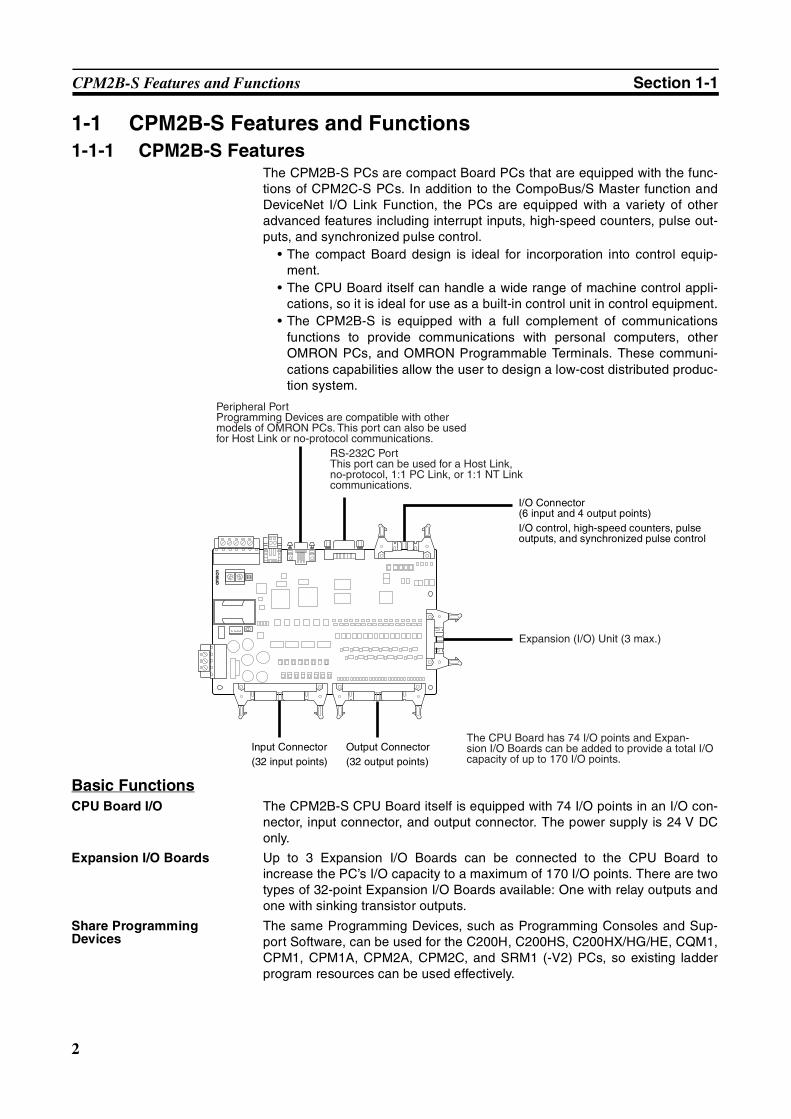
1-1 CPM2B-S Features and Functions1-1-1 CPM2B-S Features
The CPM2B-S PCs are compact Board PCs that are equipped with the func-tions of CPM2C-S PCs. In addition to the CompoBus/S Master function andDeviceNet I/O Link Function, the PCs are equipped with a variety of otheradvanced features including interrupt inputs, high-speed counters, pulse out-puts, and synchronized pulse control.
• The compact Board design is ideal for incorporation into control equip-ment.
• The CPU Board itself can handle a wide range of machine control appli-cations, so it is ideal for use as a built-in control unit in control equipment.
• The CPM2B-S is equipped with a full complement of communicationsfunctions to provide communications with personal computers, otherOMRON PCs, and OMRON Programmable Terminals. These communi-cations capabilities allow the user to design a low-cost distributed produc-tion system.
Basic FunctionsCPU Board I/O The CPM2B-S CPU Board itself is equipped with 74 I/O points in an I/O con-
nector, input connector, and output connector. The power supply is 24 V DConly.
Expansion I/O Boards Up to 3 Expansion I/O Boards can be connected to the CPU Board toincrease the PC’s I/O capacity to a maximum of 170 I/O points. There are twotypes of 32-point Expansion I/O Boards available: One with relay outputs andone with sinking transistor outputs.
Share Programming Devices
The same Programming Devices, such as Programming Consoles and Sup-port Software, can be used for the C200H, C200HS, C200HX/HG/HE, CQM1,CPM1, CPM1A, CPM2A, CPM2C, and SRM1 (-V2) PCs, so existing ladderprogram resources can be used effectively.
Peripheral PortProgramming Devices are compatible with other models of OMRON PCs. This port can also be used for Host Link or no-protocol communications.
RS-232C PortThis port can be used for a Host Link, no-protocol, 1:1 PC Link, or 1:1 NT Link communications.
Expansion (I/O) Unit (3 max.)
The CPU Board has 74 I/O points and Expan-sion I/O Boards can be added to provide a total I/O capacity of up to 170 I/O points.
Input Connector(32 input points)
Output Connector(32 output points)
I/O Connector(6 input and 4 output points)I/O control, high-speed counters, pulse outputs, and synchronized pulse control
3
CPM2B-S Features and Functions Section 1-1
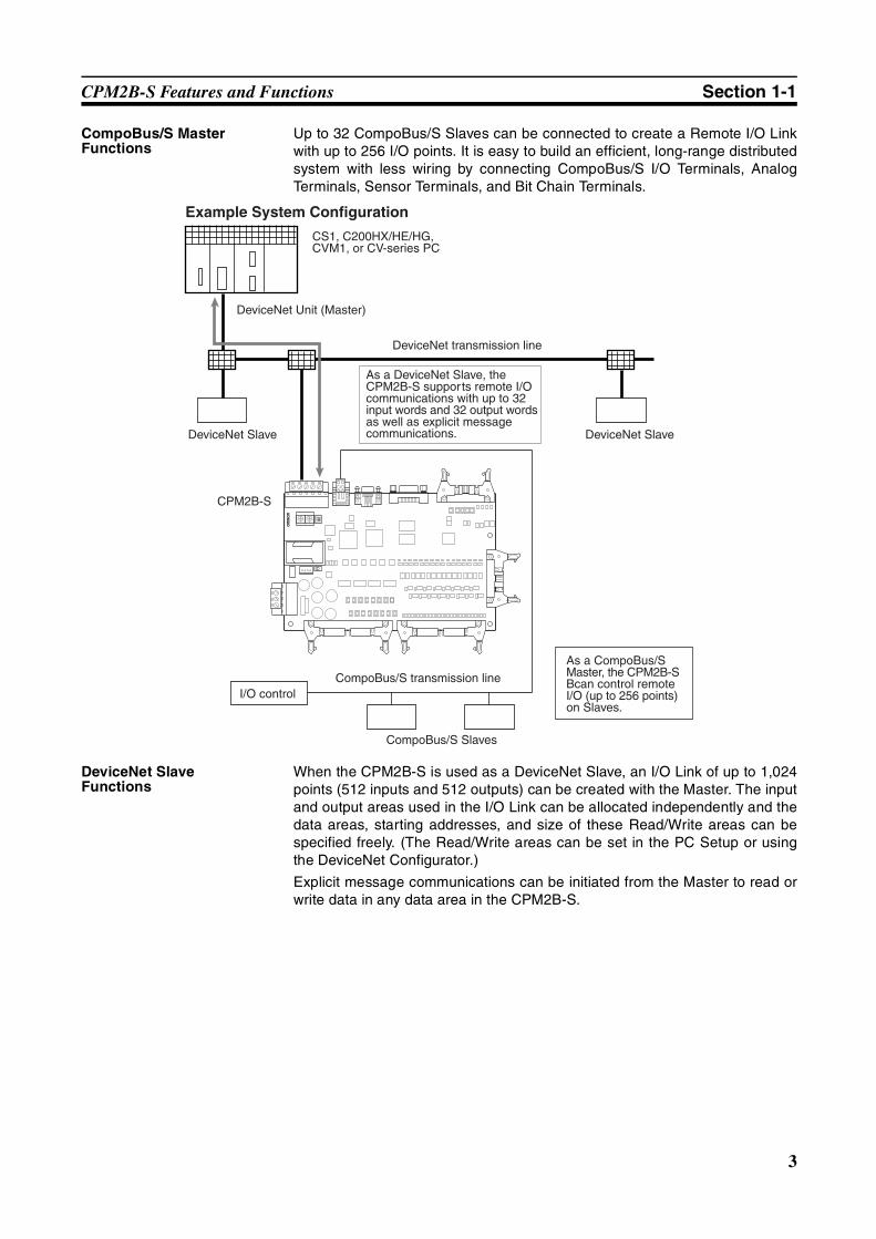
CompoBus/S Master Functions
Up to 32 CompoBus/S Slaves can be connected to create a Remote I/O Linkwith up to 256 I/O points. It is easy to build an efficient, long-range distributedsystem with less wiring by connecting CompoBus/S I/O Terminals, AnalogTerminals, Sensor Terminals, and Bit Chain Terminals.
DeviceNet Slave Functions
When the CPM2B-S is used as a DeviceNet Slave, an I/O Link of up to 1,024points (512 inputs and 512 outputs) can be created with the Master. The inputand output areas used in the I/O Link can be allocated independently and thedata areas, starting addresses, and size of these Read/Write areas can bespecified freely. (The Read/Write areas can be set in the PC Setup or usingthe DeviceNet Configurator.)
Explicit message communications can be initiated from the Master to read orwrite data in any data area in the CPM2B-S.
Example System Configuration
CS1, C200HX/HE/HG, CVM1, or CV-series PC
DeviceNet Unit (Master)
DeviceNet transmission line
DeviceNet Slave
As a DeviceNet Slave, the CPM2B-S supports remote I/O communications with up to 32 input words and 32 output words as well as explicit message communications. DeviceNet Slave
CPM2B-S
As a CompoBus/S Master, the CPM2B-S Bcan control remote I/O (up to 256 points) on Slaves.
CompoBus/S transmission lineI/O control
CompoBus/S Slaves
4
CPM2B-S Features and Functions Section 1-1
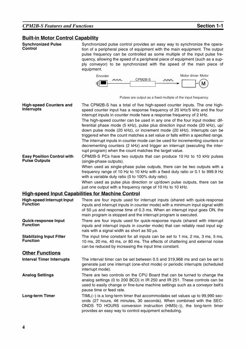
Built-in Motor Control CapabilitySynchronized Pulse Control
Synchronized pulse control provides an easy way to synchronize the opera-tion of a peripheral piece of equipment with the main equipment. The outputpulse frequency can be controlled as some multiple of the input pulse fre-quency, allowing the speed of a peripheral piece of equipment (such as a sup-ply conveyor) to be synchronized with the speed of the main piece ofequipment.
High-speed Counters and Interrupts
The CPM2B-S has a total of five high-speed counter inputs. The one high-speed counter input has a response frequency of 20 kHz/5 kHz and the fourinterrupt inputs in counter mode have a response frequency of 2 kHz.The high-speed counter can be used in any one of the four input modes: dif-ferential phase mode (5 kHz), pulse plus direction input mode (20 kHz), up/down pulse mode (20 kHz), or increment mode (20 kHz). Interrupts can betriggered when the count matches a set value or falls within a specified range.The interrupt inputs in counter mode can be used for incrementing counters ordecrementing counters (2 kHz) and trigger an interrupt (executing the inter-rupt program) when the count matches the target value.
Easy Position Control with Pulse Outputs
CPM2B-S PCs have two outputs that can produce 10 Hz to 10 kHz pulses(single-phase outputs).When used as single-phase pulse outputs, there can be two outputs with afrequency range of 10 Hz to 10 kHz with a fixed duty ratio or 0.1 to 999.9 Hzwith a variable duty ratio (0 to 100% duty ratio).When used as pulse plus direction or up/down pulse outputs, there can bejust one output with a frequency range of 10 Hz to 10 kHz.
High-speed Input Capabilities for Machine ControlHigh-speed Interrupt Input Function
There are four inputs used for interrupt inputs (shared with quick-responseinputs and interrupt inputs in counter mode) with a minimum input signal widthof 50 µs and response time of 0.3 ms. When an interrupt input goes ON, themain program is stopped and the interrupt program is executed.
Quick-response Input Function
There are four inputs used for quick-response inputs (shared with interruptinputs and interrupt inputs in counter mode) that can reliably read input sig-nals with a signal width as short as 50 µs.
Stabilizing Input Filter Function
The input time constant for all inputs can be set to 1 ms, 2 ms, 3 ms, 5 ms,10 ms, 20 ms, 40 ms, or 80 ms. The effects of chattering and external noisecan be reduced by increasing the input time constant.
Other FunctionsInterval Timer Interrupts The interval timer can be set between 0.5 and 319,968 ms and can be set to
generate just one interrupt (one-shot mode) or periodic interrupts (scheduledinterrupt mode).
Analog Settings There are two controls on the CPU Board that can be turned to change theanalog settings (0 to 200 BCD) in IR 250 and IR 251. These controls can beused to easily change or fine-tune machine settings such as a conveyor belt’spause time or feed rate.
Long-term Timer TIML(–) is a long-term timer that accommodates set values up to 99,990 sec-onds (27 hours, 46 minutes, 30 seconds). When combined with the SEC-ONDS TO HOURS conversion instruction (HMS(–)), the long-term timerprovides an easy way to control equipment scheduling.
EncoderCPM2B-S
Motor driver Motor
Pulses are output as a fixed multiple of the input frequency.
5
CPM2B-S Features and Functions Section 1-1
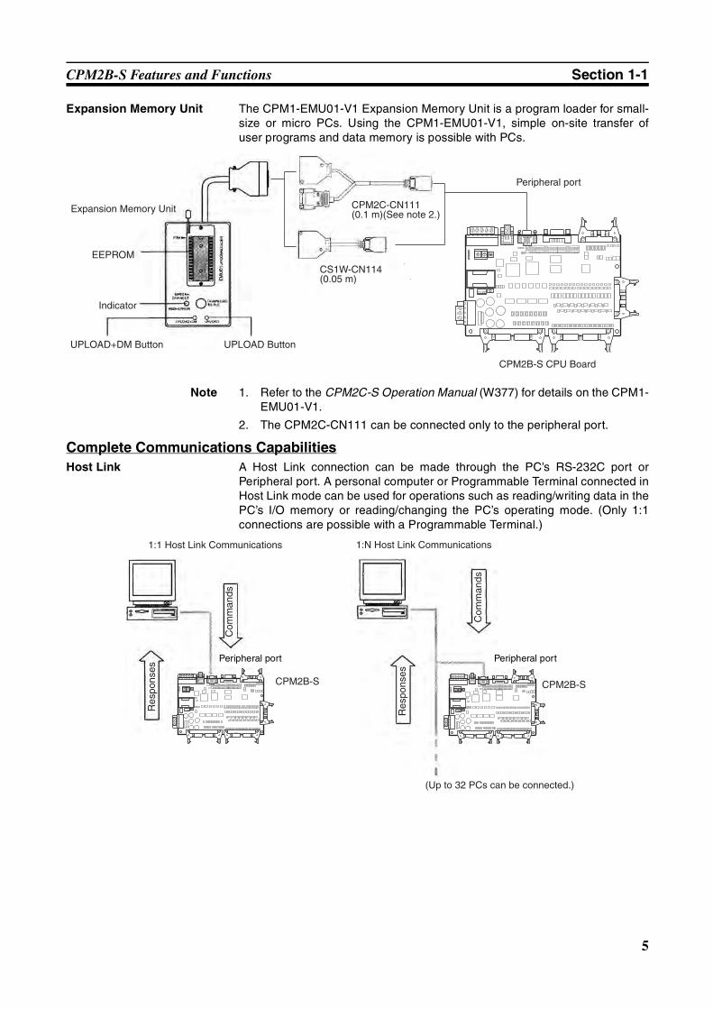
Expansion Memory Unit The CPM1-EMU01-V1 Expansion Memory Unit is a program loader for small-size or micro PCs. Using the CPM1-EMU01-V1, simple on-site transfer ofuser programs and data memory is possible with PCs.
Note 1. Refer to the CPM2C-S Operation Manual (W377) for details on the CPM1-EMU01-V1.
2. The CPM2C-CN111 can be connected only to the peripheral port.
Complete Communications CapabilitiesHost Link A Host Link connection can be made through the PC’s RS-232C port or
Peripheral port. A personal computer or Programmable Terminal connected inHost Link mode can be used for operations such as reading/writing data in thePC’s I/O memory or reading/changing the PC’s operating mode. (Only 1:1connections are possible with a Programmable Terminal.)
Expansion Memory Unit
Indicator
UPLOAD+DM Button UPLOAD Button
EEPROM
CPM2C-CN111(0.1 m)(See note 2.)
CS1W-CN114(0.05 m)
CPM2B-S CPU Board
Peripheral port
IN000CH IN001CH IN002CH
OUT010CH OUT011CH OUT012CH
1:1 Host Link Communications
CPM2B-S
Com
man
ds
Res
pons
es
1:N Host Link Communications
(Up to 32 PCs can be connected.)
Com
man
ds
Res
pons
es
CPM2B-SIN000CH IN001CH IN002CH
OUT010CH OUT011CH OUT012CH
IN000CH IN001CH IN002CH
OUT010CH OUT011CH OUT012CH
Peripheral port Peripheral port
6
CPM2B-S Features and Functions Section 1-1
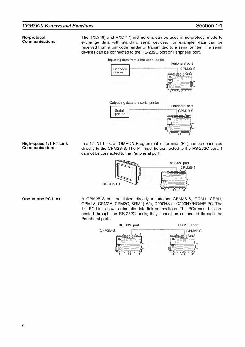
No-protocol Communications
The TXD(48) and RXD(47) instructions can be used in no-protocol mode toexchange data with standard serial devices. For example, data can bereceived from a bar code reader or transmitted to a serial printer. The serialdevices can be connected to the RS-232C port or Peripheral port.
High-speed 1:1 NT Link Communications
In a 1:1 NT Link, an OMRON Programmable Terminal (PT) can be connecteddirectly to the CPM2B-S. The PT must be connected to the RS-232C port; itcannot be connected to the Peripheral port.
One-to-one PC Link A CPM2B-S can be linked directly to another CPM2B-S, CQM1, CPM1,CPM1A, CPM2A, CPM2C, SRM1(-V2), C200HS or C200HX/HG/HE PC. The1:1 PC Link allows automatic data link connections. The PCs must be con-nected through the RS-232C ports; they cannot be connected through thePeripheral ports.
Bar code reader
Serial printer
Inputting data from a bar code reader
Outputting data to a serial printer
CPM2B-S
CPM2B-S
IN000CH IN001CH IN002CH
OUT010CH OUT011CH OUT012CH
IN000CH IN001CH IN002CH
OUT010CH OUT011CH OUT012CH
Peripheral port
Peripheral port
OMRON PT
CPM2B-S
IN000CH IN001CH IN002CH
OUT010CH OUT011CH OUT012CH
RS-232C port
CPM2B-S CPM2B-S
IN000CH IN001CH IN002CH
OUT010CH OUT011CH OUT012CH
IN000CH IN001CH IN002CH
OUT010CH OUT011CH OUT012CH
RS-232C port RS-232C port
7
CPM2B-S Features and Functions Section 1-1
1-1-2 Overview of CPM2B-S FunctionsMain function Variations/Details
CompoBus/S Master func-tions
• Remote I/O devices can be allocated up to 256 I/O points (128 inputs and 128 outputs) in input area IR 020 to IR 027 and output area IR 030 to IR 037.
• The node numbers can be set to 0 to 7 (128-point mode) or 0 to 15 (256-point mode).
• The communications mode can be set to high-speed mode (max. length 100 m) or long-distance mode (max. length 500 m).
DeviceNet Slave functions
• Up to 64 words (32 input words and 32 output words) can be allocated to the DeviceNet Master’s I/O. The Master’s I/O can be allocated to the following data areas.
IR 000 to IR 049IR 200 to IR 227DM 0000 to DM 2047LR 00 to LR 15HR 00 to HR 19AR 00 to AR 23 (CPM2B-S → Master; read-only)TC 000 to TC 255
• Explicit message communications are supported. Any CPM2B-S data area can be accessed from the DeviceNet Master.
• The communications speed can be set to 500 kbps (total network length 100 m max.), 250 kbps (total network length 250 m max.), or 125 kbps (total network length 500 m max.).
Interrupts Interrupt inputs4 inputs, see note 1.
Response time: 50 µs
Interval timer interrupts1 input
Set value: 0.5 to 319,968 msPrecision: 0.1 ms
Scheduled interrupts
One-shot interrupt
High-speed counters High-speed counter1 input, see note 2.
Differential phase mode (5 kHz)Pulse plus direction input mode (20 kHz)Up/down input mode (20 kHz)Increment mode (20 kHz)
No interrupt
Count-check interrupt
(An interrupt can be generated when the count equals the set value or the count lies within a preset range.)
Interrupt inputs in counter mode4 inputs, see note 1.
Incrementing counter (2 kHz)Decrementing counter (2 kHz)
No interrupt
Count-up interrupt
Pulse outputs 2 outputs:Single-phase pulse output without acceleration/deceleration (See note 3.)10 Hz to 10 kHz
2 outputs:Variable duty ratio pulse output (See note 3.)0.1 to 999.9 Hz, duty ratio 0 to 100%
1 output:Pulse output with trapezoidal acceleration/deceleration (See note 3.)Pulse plus direction output, up/down pulse output, 10 Hz to 10 kHz
Synchronized pulse control 1 point, see notes 2 and 3.
Input frequency range: 10 to 500 Hz, 20 Hz to 1 kHz, or 300 Hz to 20 kHzOutput frequency range: 10 Hz to 10 kHz
Quick-response input 4 inputs, see note 1.
Maximum input signal width: 50 µs
Input time constant Determines the input time constant for all inputs except for those for IR 001 and IR 002. (Settings: 1, 2, 3, 5, 10, 20, 40, or 80 ms)
Error log Records the error code.
8
System Configurations Section 1-2
Note 1. These four inputs are shared by interrupt inputs, interrupt inputs in countermode, and quick-response inputs, but each input can be used for only onepurpose.
2. This input is shared by the high-speed counter and synchronized pulsecontrol functions.
3. This output is shared by the pulse output and synchronized pulse controlfunctions. These functions can be used with transistor outputs only.
1-2 System Configurations
1-2-1 CPU Board
1-2-2 Expansion I/O BoardsUp to 3 Expansion I/O Boards can be connected to the CPU Board.
A PC with 170 I/O points (the maximum) can be assembled by connectingthree Expansion I/O Boards. The following configuration provides 86 inputsand 84 sinking transistor outputs:
IN000CH IN001CH IN002CH
OUT010CH OUT011CH OUT012CH
CPU Board Inputs Outputs Battery RS-232C port
Model
74 I/O points
(38 inputs, 36 outputs)
32 in input connector,6 in I/O connector
32 in output connector,4 in I/O connector
Optional Yes CPM2B-S001M-DRT
Expansion I/O Board with 32 I/O points(Relay outputs)
Expansion I/O Board with 32 I/O points(Transistor outputs)
Expansion connector
Expansion connector
CPU Board
Expansion I/O Board
CPM2B-S(38 inputs, 36 outputs)
CPM2B-32EDT(16 inputs, 16 outputs) 1 Board + 3 Boards = 86 inputs, 84 outputs
9
System Configurations Section 1-2
Expansion I/O Boards
Note When an NT-AL001-E Adapter is connected to the RS-232C port, only oneExpansion I/O Board can be connected because of power supply limitations.Refer to the CPM2B Operation Manual (W371) for details on Expansion I/OBoard specifications and mounting instructions.
1-2-3 Connecting a Programming ConsoleA Programming Console can be connected to the CPM2B-S CPU Board’speripheral port, as shown below.
Note 1. Only the peripheral port connector can be used when a CPM2C-CN111Connecting Cable is connected.
2. Refer to the CPM2B Operation Manual (W371) or the CPM2C-S OperationManual (W377) for Programming Console operating procedures.
Expansion I/O Board
Inputs Outputs Model
32 I/O points
(16 inputs, 16 outputs)
16 inputs, 24 V DC 16 relay outputs(terminal block)
CPM2B-32EDR
16 inputs, 24 V DC 16 sinking transistor outputs (connector)
CPM2B-32EDT
Peripheral port
CPM2C-CN111 Connecting Cable(0.1 m) (See note 2.)
CS1W-CN114 Connecting Cable (0.05 m)
CQM1-PRO01-E
CS1W-CN224 (2 m) or CS1W-CN624 (4 m) Connecting Cable
CPM2B-S CPU Board
C200H-PRO27-E
C200H-CN222 (2 m) or C200H-CN422 (4 m) Connecting Cable
Attached cable (2 m) Peripheral port
connector
CQM1H-PRO01-E
Dip Switch
IN000CH IN001CH IN002CH
OUT010CH OUT011CH OUT012CH
10
System Configurations Section 1-2
1-2-4 Support SoftwareA personal computer running the CX-Programmer or SYSMAC-CPT SupportSoftware (in MS Windows) or the SSS (in MS-DOS) can be connected to theCPU Board’s Peripheral port or RS-232C port. Refer to 1-2-5 One-to-oneComputer Connections for details on the computer connection.
The setting of DIP Switch pin 3 determines whether the communications set-tings in the PC Setup or the standard settings will be used, as shown in thefollowing table.
When using the SSS, set the PC Model to “CQM1.” When using the SYS-MAC-CPT, set the PC Model to “CQM1” with the “CPU43” CPU version.
1-2-5 One-to-one Computer ConnectionsUse one of the connecting cables shown in the following diagram to connect apersonal computer with Support Software to the CPM2B-S for a 1:1 Host Linkcommunications or no-protocol (serial) communications.
Note 1. The CQM1-CIF11 Connecting Cable cannot be used.
2. Refer to Appendix A Standard Models for details on the Support Softwarethat can be used with the CPM2B-S.
Pin 3 setting
Communications settings
Peripheral port RS-232C port
ON Standard settings (The standard settings and PC Setup default settings are Host Link communications at 9,600 bps with 1 start bit, 7-bit data, 2 stop bits, and even parity.)
OFF PC Setup settings in DM 6650 and DM 6651
PC Setup settings in DM 6645 and DM 6646
RS-232C port (D-sub 9-pin)
Connecting Cable
XW2Z-200S-V (2 m)XW2Z-500S-V (5 m)
IBM PC/AT or compatible computer
RS-232C Port Connection
Peripheral port
CPM2B-S CPU Board
Connecting CableXW2Z-200S-V (2 m)XW2Z-500S-V (5 m)
IBM PC/AT or compatible computer
Peripheral Port Connection
CS1W-CN114 (0.05 m)
CQM1-CIF02 (3.3 m)
CPM1-CIF01 RS-232C Adapter
IN000CH IN001CH IN002CH
OUT010CH OUT011CH OUT012CH
IN000CH IN001CH IN002CH
OUT010CH OUT011CH OUT012CH
CPM2B-S CPU Board
11
System Configurations Section 1-2
1-2-6 One-to-N Computer ConnectionsUp to 32 OMRON PCs, including CPM2B-S PCs, can be connected to a hostcomputer.
Using the RS-232C Port
Using the Peripheral Port
Note 1. The NT-AL001-E must be supplied externally with 5 V DC. When an NT-AL001-E is connected to a CPM2B-S PC, pin 6 of the CPM2B-S’s RS-232C port supplies +5 V DC and an external power supply is not neces-sary. When the NT-AL001-E is connected to a host computer, it is neces-sary to supply 5 V DC from an external power supply.
If an NT-AL001-E is connected to the CPM2B-S’s RS-232C port, only oneExpansion I/O Board can be connected to the CPU Board because the NT-AL001-E draws its 5-V DC power from the CPU Board.
Use an XW2Z-070T-1 (0.7 m) or XW2Z-200T-1 (2 m) cable to connect theNT-AL001-E to the CPM2B-S’s RS-232C port.
2. The 3G2A9-AL004-E requires an external AC power supply (110 V AC or220 V AC).
3. The CPM1-CIF11 is supplied +5 V DC from the peripheral port so an ex-ternal power supply is not necessary.
RS-422 (Total length: 500 m max.)
NT-AL001-E(See note 1.)
NT-AL001-E(See note 1.)
NT-AL001-E(See note 1.)
Up to 32 PCs
CPM2B-S CPU Board CPM2B-S CPU Board CPM2B-S CPU Board
3G2A9-AL004-E or NT-AL001-E (requires +5 V)(See notes 1 and 2.)
Connecting CableXW2Z-@00S-V
IBM PC/AT or compatible computer
IN000CH IN001CH IN002CH
OUT010CH OUT011CH OUT012CH
IN000CH IN001CH IN002CH
OUT010CH OUT011CH OUT012CH
IN000CH IN001CH IN002CH
OUT010CH OUT011CH OUT012CH
RS-422 (Total length: 500 m max.)
CPM1-CIF11 (See note 3.)
Up to 32 PCs
CPM2B-S CPU Board CPM2B-S CPU Board CPM2B-S CPU Board
3G2A9-AL004-E or NT-AL001-E (requires +5 V)(See notes 1.)
Connecting CableXW2Z-@00S-V
CPM1-CIF11 (See note 3.)
CPM1-CIF11 (See note 3.)
CS1W-CN114 CS1W-CN114 CS1W-CN114
IBM PC/AT or compatible computer
IN000CH IN001CH IN002CH
OUT010CH OUT011CH OUT012CH
IN000CH IN001CH IN002CH
OUT010CH OUT011CH OUT012CH
IN000CH IN001CH IN002CH
OUT010CH OUT011CH OUT012CH
12
System Configurations Section 1-2
1-2-7 OMRON PT ConnectionsIn a 1:1 NT Link, a CPM2B-S can be connected directly to a ProgrammableTerminal through the RS-232C port. (The Programmable Terminal cannot beconnected directly to the peripheral port.)
An OMRON PT can also be connected to the CPM2B-S with a host link con-nection. Either the RS-232C port or peripheral port can be used for a host linkconnection.
Connecting Cable
XW2Z-200T (2 m)XW2Z-500T (5 m)
NT-AL001-ERS-232C Adapter
XW2Z-070T-1 (0.7 m)XW2Z-200T-1 (2 m)
CS1W-CN114(0.05 m) CPM2B-S CPU Board
OMRON Programmable Terminal
RS-232C port (D-sub 9-pin)
CPM1-CIF02RS-422 Adapter
RS-422connection
Peripheral port
CPM1-CIF01RS-232C Adapter
Connecting CableXW2Z-200T (2 m)XW2Z-500T (5 m)
IN000CH IN001CH IN002CH
OUT010CH OUT011CH OUT012CH
13
System Configurations Section 1-2
1-2-8 One-to-one PC Link ConnectionsA CPM2B-S can be linked to another CPM2B-S, a CQM1, CPM1, CPM1A,CPM2A, CPM2C, CPM2C-S, CPM2B, SRM1 (-V2) or a C200HS or C200HX/HG/HE PC. The PCs must be connected through the RS-232C ports; theycannot be connected through the Peripheral ports.
1:1 Link Master
Connecting CableXW2Z-200T (2 m)XW2Z-500T (5 m)
RS-232C port(D-sub 9-pin)
RS-232C port (D-sub 9-pin)
1:1 Link Slave
OMRON PC (CQM1, CPM1, CPM1A, CPM2A, CPM2B, CPM2C, CPM2C-S,SRM1(-V2), C200HS, or C200HX/HG/HE)
OMRON PC (CQM1, CPM1, CPM1A, CPM2A, CPM2B, CPM2C, CPM2C-S,SRM1(-V2), C200HS, or C200HX/HG/HE)
CPM2B-S CPU Board CPM2B-S CPU Board
IN000CH IN001CH IN002CH
OUT010CH OUT011CH OUT012CH
IN000CH IN001CH IN002CH
OUT010CH OUT011CH OUT012CH
14
Structure and Operation Section 1-3
1-3 Structure and Operation
1-3-1 CPU Board StructureThe following diagram shows the internal structure of the CPU Board.
I/O Memory The program reads and writes data in this memory area during execution.Part of the I/O memory contains the bits that reflect the status of the PC’sinputs and outputs. Parts of the I/O memory are cleared when the power isturned ON and other parts are retained.
Note Refer to SECTION 4 Memory Areas for more details on I/O memory.
Program This is the program written by the user. The CPM2B-S executes the programcyclically. (Refer to 1-3-5 Cyclic Operation and Interrupts for details.)
The program can be divided broadly into two parts: the “main program” that isexecuted cyclically and the “interrupt programs” that are executed only whenthe corresponding interrupt is generated.
PC Setup The PC Setup contains various startup and operating parameters. The PCSetup parameters can be changed from a Programming Device only; theycannot be changed from the program.
Some parameters are accessed only when PC’s power supply is turned onand others are accessed regularly while the power is on. It will be necessaryto turn the power off and then on again to enable a new setting if the parame-ter is accessed only when the power is turned on.
Note Refer to 4-6 PC Setup for more details.
Communications Switches (Dip Switch Pin 1 to 3)
The Communications Switches (Dip Switch Pin 1 to 3) determine whether theperipheral port and RS-232C port operate with the standard communications
External input devices
I/O memory
Program
PC Setup
RS-232C port
Settings
Settings
Settings
External output devices
Communications switches
DeviceNet Master
CompoBus/S Slaves
Dev
iceN
etin
terf
ace
Com
poB
us/S
inte
rfac
e
Inpu
t circ
uits
Out
put c
ircui
ts
Peripheral port
15
Structure and Operation Section 1-3
settings or the communications settings in the PC Setup. Refer to 2-2 BoardComponents and their Functions for more details.
1-3-2 Operating ModesCPM2B-S CPU Boards have 3 operating modes: PROGRAM, MONITOR, andRUN.
PROGRAM Mode The program cannot be executed in PROGRAM mode. This mode is used toperform the following operations in preparation for program execution
• Changing initial/operating parameters such as those in the PC Setup
• Writing, transferring, or checking the program
• Checking wiring by force-setting and force-resetting I/O bits
!Caution The PC continues to refresh I/O bits even if the PC is in PROGRAM mode, sodevices connected to output points on the CPU Board or Expansion I/OBoards may operate unexpectedly if the corresponding output bit is turned ONby changing the contents of I/O memory from a Programming Device.
MONITOR Mode The program is executed in MONITOR mode and the following operations canbe performed from a Programming Device. In general, MONITOR mode isused to debug the program, test operation, and make adjustments.
• Online editing
• Monitoring I/O memory during operation
• Force-setting/force-resetting I/O bits, changing set values, and changingpresent values during operation
RUN Mode The program is executed at normal speed in RUN mode. Operations such asonline editing, force-setting/force-resetting I/O bits, and changing set values/present values cannot be performed in RUN mode, but the status of I/O bitscan be monitored.
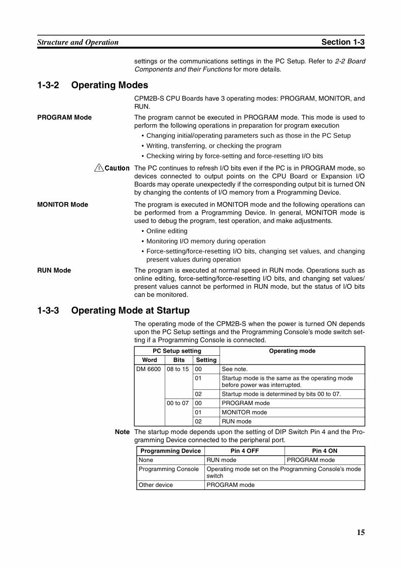
1-3-3 Operating Mode at StartupThe operating mode of the CPM2B-S when the power is turned ON dependsupon the PC Setup settings and the Programming Console’s mode switch set-ting if a Programming Console is connected.
Note The startup mode depends upon the setting of DIP Switch Pin 4 and the Pro-gramming Device connected to the peripheral port.
PC Setup setting Operating mode
Word Bits Setting
DM 6600 08 to 15 00 See note.
01 Startup mode is the same as the operating mode before power was interrupted.
02 Startup mode is determined by bits 00 to 07.
00 to 07 00 PROGRAM mode
01 MONITOR mode
02 RUN mode
Programming Device Pin 4 OFF Pin 4 ON
None RUN mode PROGRAM mode
Programming Console Operating mode set on the Programming Console’s mode switch
Other device PROGRAM mode
16
Structure and Operation Section 1-3
1-3-4 PC Operation at StartupTime Required for Initialization
The time required for startup initialization depends on several factors, such asthe operating conditions (including power supply voltage, system configura-tion, and ambient temperature) and the program contents.
Power OFF OperationMinimum Power Supply Voltage
The PC will stop and all outputs will be turned OFF if the power supply voltagefalls below 85% of the rated value.
Momentary Power Interruption
A power interruption will not be detected and CPU Board operation will con-tinue if the power interruption lasts less than 2 ms for a DC power supply.A power interruption may or may not be detected for power interruptionssomewhat longer than 2 ms for a DC power supply.When a power interruption is detected, the CPU Board will stop operating andall outputs will be turned OFF.
Automatic Reset
Operation will restart automatically when the power supply voltage is restoredto more than 85% of the rated voltage.
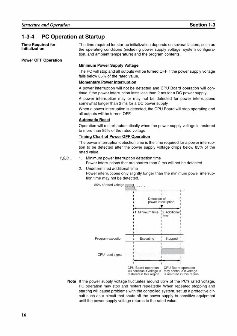
Timing Chart of Power OFF Operation
The power interruption detection time is the time required for a power interrup-tion to be detected after the power supply voltage drops below 85% of therated value.
1,2,3... 1. Minimum power interruption detection timePower interruptions that are shorter than 2 ms will not be detected.
2. Undetermined additional timePower interruptions only slightly longer than the minimum power interrup-tion time may not be detected.
Note If the power supply voltage fluctuates around 85% of the PC’s rated voltage,PC operation may stop and restart repeatedly. When repeated stopping andstarting will cause problems with the controlled system, set up a protective cir-cuit such as a circuit that shuts off the power supply to sensitive equipmentuntil the power supply voltage returns to the rated value.
85% of rated voltage
Program execution
CPU reset signal
Detection ofpower interruption
Executing Stopped
1. Minimum time 2. Additional time
CPU Board operation will continue if voltage is restored in this region.
CPU Board operation may continue if voltage is restored in this region.
17
Structure and Operation Section 1-3
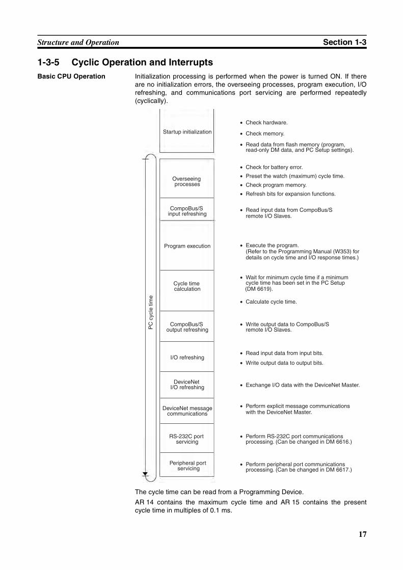
1-3-5 Cyclic Operation and InterruptsBasic CPU Operation Initialization processing is performed when the power is turned ON. If there
are no initialization errors, the overseeing processes, program execution, I/Orefreshing, and communications port servicing are performed repeatedly(cyclically).
The cycle time can be read from a Programming Device.
AR 14 contains the maximum cycle time and AR 15 contains the presentcycle time in multiples of 0.1 ms.
Startup initialization
Overseeing processes
Program execution
Cycle time calculation
I/O refreshing
RS-232C port servicing
Peripheral port servicing
• Check hardware.
• Check memory.
• Read data from flash memory (program, read-only DM data, and PC Setup settings).
• Check for battery error.
• Preset the watch (maximum) cycle time.
• Check program memory.
• Refresh bits for expansion functions.
• Execute the program.(Refer to the Programming Manual (W353) for details on cycle time and I/O response times.)
• Wait for minimum cycle time if a minimum cycle time has been set in the PC Setup (DM 6619).
• Calculate cycle time.
• Read input data from input bits.
• Write output data to output bits.
• Perform RS-232C port communications processing. (Can be changed in DM 6616.)
• Perform peripheral port communications processing. (Can be changed in DM 6617.)
• Read input data from CompoBus/S remote I/O Slaves.
CompoBus/S input refreshing
• Write output data to CompoBus/S remote I/O Slaves.
CompoBus/S output refreshing
• Perform explicit message communications with the DeviceNet Master.
DeviceNet message communications
DeviceNet I/O refreshing • Exchange I/O data with the DeviceNet Master.
PC
cyc
le ti
me
18
Structure and Operation Section 1-3
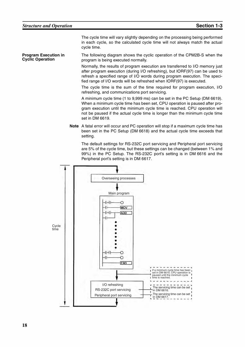
The cycle time will vary slightly depending on the processing being performedin each cycle, so the calculated cycle time will not always match the actualcycle time.
Program Execution in Cyclic Operation
The following diagram shows the cyclic operation of the CPM2B-S when theprogram is being executed normally.
Normally, the results of program execution are transferred to I/O memory justafter program execution (during I/O refreshing), but IORF(97) can be used torefresh a specified range of I/O words during program execution. The speci-fied range of I/O words will be refreshed when IORF(97) is executed.
The cycle time is the sum of the time required for program execution, I/Orefreshing, and communications port servicing.
A minimum cycle time (1 to 9,999 ms) can be set in the PC Setup (DM 6619).When a minimum cycle time has been set, CPU operation is paused after pro-gram execution until the minimum cycle time is reached. CPU operation willnot be paused if the actual cycle time is longer than the minimum cycle timeset in DM 6619.
Note A fatal error will occur and PC operation will stop if a maximum cycle time hasbeen set in the PC Setup (DM 6618) and the actual cycle time exceeds thatsetting.
The default settings for RS-232C port servicing and Peripheral port servicingare 5% of the cycle time, but these settings can be changed (between 1% and99%) in the PC Setup. The RS-232C port’s setting is in DM 6616 and thePeripheral port’s setting is in DM 6617.
Cycletime
Overseeing processes
Main program
I/O refreshing
RS-232C port servicing
Peripheral port servicing
If a minimum cycle time has been set in DM 6619, CPU operation is paused until the minimum cycle time is reached.
The servicing time can be set in DM 6616.The servicing time can be set in DM 6617.
19
Structure and Operation Section 1-3
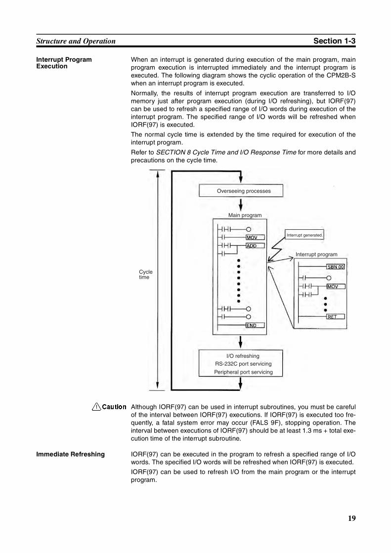
Interrupt Program Execution
When an interrupt is generated during execution of the main program, mainprogram execution is interrupted immediately and the interrupt program isexecuted. The following diagram shows the cyclic operation of the CPM2B-Swhen an interrupt program is executed.
Normally, the results of interrupt program execution are transferred to I/Omemory just after program execution (during I/O refreshing), but IORF(97)can be used to refresh a specified range of I/O words during execution of theinterrupt program. The specified range of I/O words will be refreshed whenIORF(97) is executed.
The normal cycle time is extended by the time required for execution of theinterrupt program.
Refer to SECTION 8 Cycle Time and I/O Response Time for more details andprecautions on the cycle time.
!Caution Although IORF(97) can be used in interrupt subroutines, you must be carefulof the interval between IORF(97) executions. If IORF(97) is executed too fre-quently, a fatal system error may occur (FALS 9F), stopping operation. Theinterval between executions of IORF(97) should be at least 1.3 ms + total exe-cution time of the interrupt subroutine.
Immediate Refreshing IORF(97) can be executed in the program to refresh a specified range of I/Owords. The specified I/O words will be refreshed when IORF(97) is executed.
IORF(97) can be used to refresh I/O from the main program or the interruptprogram.
Cycletime
Overseeing processes
Main program
I/O refreshingRS-232C port servicing
Peripheral port servicing
Interrupt generated.
Interrupt program
20
Structure and Operation Section 1-3
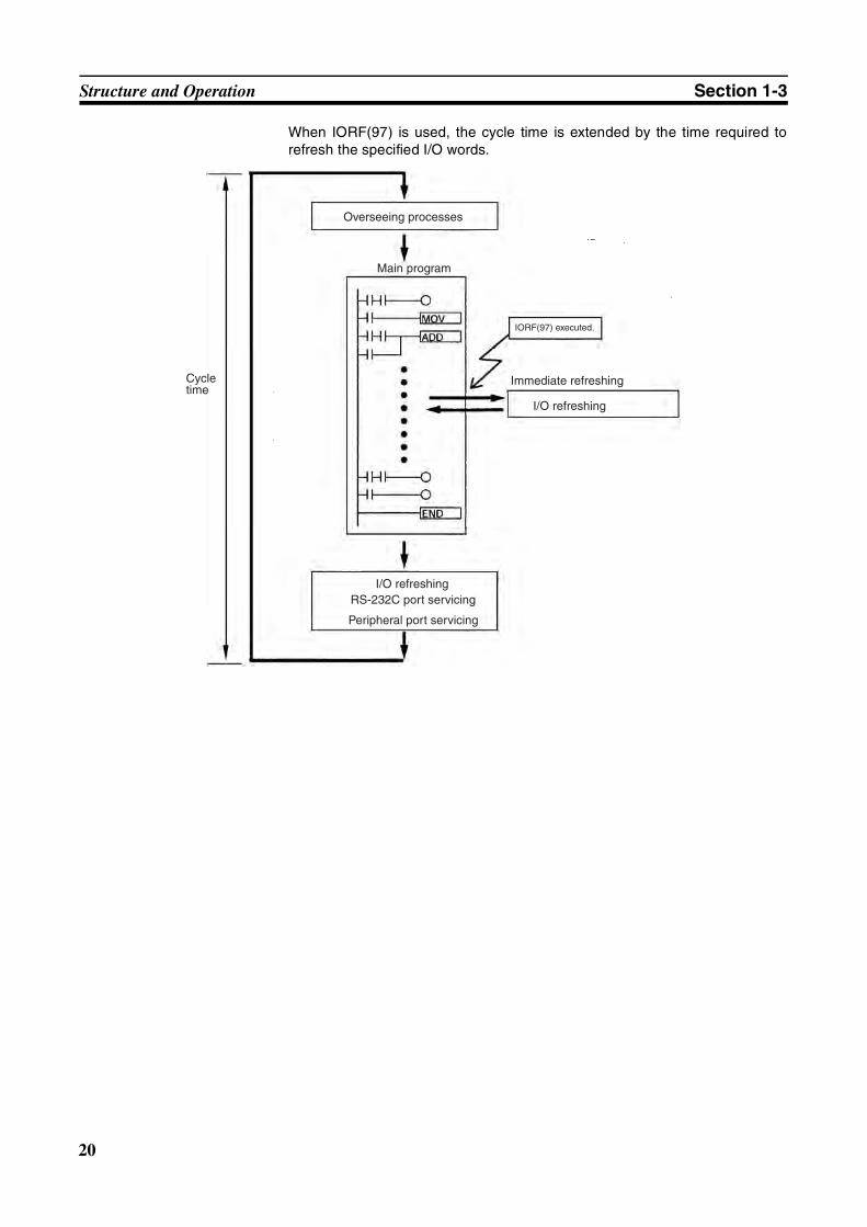
When IORF(97) is used, the cycle time is extended by the time required torefresh the specified I/O words.
Cycletime
Overseeing processes
Main program
I/O refreshingRS-232C port servicing
Peripheral port servicing
IORF(97) executed.
Immediate refreshing
I/O refreshing
21
SECTION 2Board Specifications and Components
This section provides the technical specifications of the CPM2B-S Boards and describes the main components of theBoards.
2-1 Specifications . . . . . . . . . . . . . . . . . . . . . . . . . . . . . . . . . . . . . . . . . . . . . . . . . 22
2-1-1 General Specifications . . . . . . . . . . . . . . . . . . . . . . . . . . . . . . . . . . . 22
2-1-2 Characteristics . . . . . . . . . . . . . . . . . . . . . . . . . . . . . . . . . . . . . . . . . 23
2-1-3 I/O Specifications. . . . . . . . . . . . . . . . . . . . . . . . . . . . . . . . . . . . . . . 25
2-2 Board Components and their Functions . . . . . . . . . . . . . . . . . . . . . . . . . . . . . 28
2-2-1 CPU Board Components . . . . . . . . . . . . . . . . . . . . . . . . . . . . . . . . . 28
22
Specifications Section 2-1
2-1 Specifications
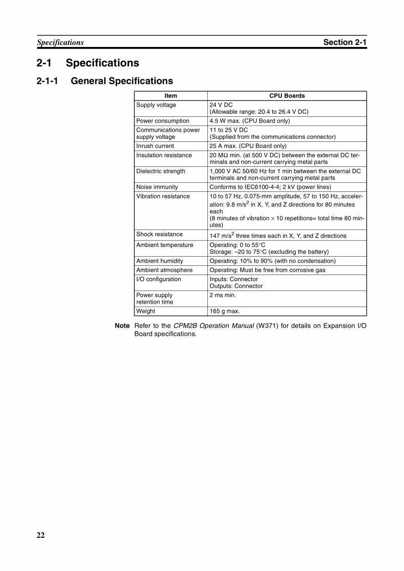
2-1-1 General Specifications
Note Refer to the CPM2B Operation Manual (W371) for details on Expansion I/OBoard specifications.
Item CPU Boards
Supply voltage 24 V DC(Allowable range: 20.4 to 26.4 V DC)
Power consumption 4.5 W max. (CPU Board only)
Communications power supply voltage
11 to 25 V DC(Supplied from the communications connector)
Inrush current 25 A max. (CPU Board only)
Insulation resistance 20 MΩ min. (at 500 V DC) between the external DC ter-minals and non-current carrying metal parts
Dielectric strength 1,000 V AC 50/60 Hz for 1 min between the external DC terminals and non-current carrying metal parts
Noise immunity Conforms to IEC6100-4-4; 2 kV (power lines)
Vibration resistance 10 to 57 Hz, 0.075-mm amplitude, 57 to 150 Hz, acceler-ation: 9.8 m/s2 in X, Y, and Z directions for 80 minutes each(8 minutes of vibration × 10 repetitions= total time 80 min-utes)
Shock resistance 147 m/s2 three times each in X, Y, and Z directions
Ambient temperature Operating: 0 to 55°CStorage: –20 to 75°C (excluding the battery)
Ambient humidity Operating: 10% to 90% (with no condensation)
Ambient atmosphere Operating: Must be free from corrosive gas
I/O configuration Inputs: ConnectorOutputs: Connector
Power supply retention time
2 ms min.
Weight 165 g max.
23
Specifications Section 2-1
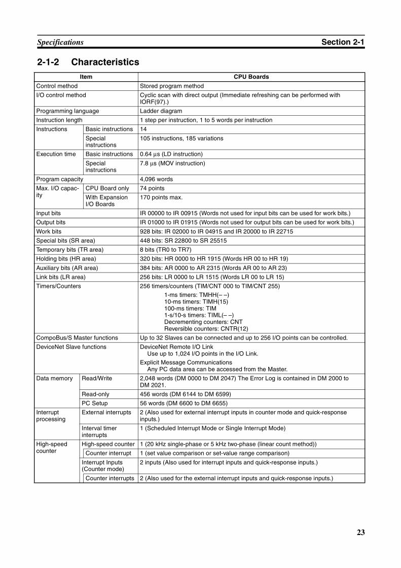
2-1-2 CharacteristicsItem CPU Boards
Control method Stored program method
I/O control method Cyclic scan with direct output (Immediate refreshing can be performed with IORF(97).)
Programming language Ladder diagram
Instruction length 1 step per instruction, 1 to 5 words per instruction
Instructions Basic instructions 14
Special instructions
105 instructions, 185 variations
Execution time Basic instructions 0.64 µs (LD instruction)
Special instructions
7.8 µs (MOV instruction)
Program capacity 4,096 words
Max. I/O capac-ity
CPU Board only 74 points
With ExpansionI/O Boards
170 points max.
Input bits IR 00000 to IR 00915 (Words not used for input bits can be used for work bits.)
Output bits IR 01000 to IR 01915 (Words not used for output bits can be used for work bits.)
Work bits 928 bits: IR 02000 to IR 04915 and IR 20000 to IR 22715
Special bits (SR area) 448 bits: SR 22800 to SR 25515
Temporary bits (TR area) 8 bits (TR0 to TR7)
Holding bits (HR area) 320 bits: HR 0000 to HR 1915 (Words HR 00 to HR 19)
Auxiliary bits (AR area) 384 bits: AR 0000 to AR 2315 (Words AR 00 to AR 23)
Link bits (LR area) 256 bits: LR 0000 to LR 1515 (Words LR 00 to LR 15)
Timers/Counters 256 timers/counters (TIM/CNT 000 to TIM/CNT 255)
1-ms timers: TMHH(– –)10-ms timers: TIMH(15)100-ms timers: TIM1-s/10-s timers: TIML(– –)Decrementing counters: CNTReversible counters: CNTR(12)
CompoBus/S Master functions Up to 32 Slaves can be connected and up to 256 I/O points can be controlled.
DeviceNet Slave functions DeviceNet Remote I/O LinkUse up to 1,024 I/O points in the I/O Link.
Explicit Message CommunicationsAny PC data area can be accessed from the Master.
Data memory Read/Write 2,048 words (DM 0000 to DM 2047) The Error Log is contained in DM 2000 to DM 2021.
Read-only 456 words (DM 6144 to DM 6599)
PC Setup 56 words (DM 6600 to DM 6655)
Interrupt processing
External interrupts 2 (Also used for external interrupt inputs in counter mode and quick-response inputs.)
Interval timer interrupts
1 (Scheduled Interrupt Mode or Single Interrupt Mode)
High-speed counter
High-speed counter 1 (20 kHz single-phase or 5 kHz two-phase (linear count method))
Counter interrupt 1 (set value comparison or set-value range comparison)
Interrupt Inputs(Counter mode)
2 inputs (Also used for interrupt inputs and quick-response inputs.)
Counter interrupts 2 (Also used for the external interrupt inputs and quick-response inputs.)
24
Specifications Section 2-1
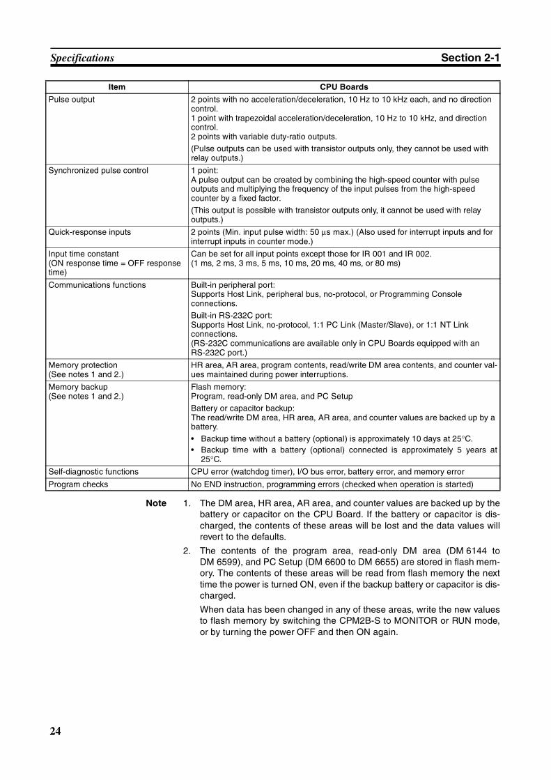
Note 1. The DM area, HR area, AR area, and counter values are backed up by thebattery or capacitor on the CPU Board. If the battery or capacitor is dis-charged, the contents of these areas will be lost and the data values willrevert to the defaults.
2. The contents of the program area, read-only DM area (DM 6144 toDM 6599), and PC Setup (DM 6600 to DM 6655) are stored in flash mem-ory. The contents of these areas will be read from flash memory the nexttime the power is turned ON, even if the backup battery or capacitor is dis-charged.
When data has been changed in any of these areas, write the new valuesto flash memory by switching the CPM2B-S to MONITOR or RUN mode,or by turning the power OFF and then ON again.
Pulse output 2 points with no acceleration/deceleration, 10 Hz to 10 kHz each, and no direction control.1 point with trapezoidal acceleration/deceleration, 10 Hz to 10 kHz, and direction control.2 points with variable duty-ratio outputs.
(Pulse outputs can be used with transistor outputs only, they cannot be used with relay outputs.)
Synchronized pulse control 1 point:A pulse output can be created by combining the high-speed counter with pulse outputs and multiplying the frequency of the input pulses from the high-speed counter by a fixed factor.
(This output is possible with transistor outputs only, it cannot be used with relayoutputs.)
Quick-response inputs 2 points (Min. input pulse width: 50 µs max.) (Also used for interrupt inputs and for interrupt inputs in counter mode.)
Input time constant(ON response time = OFF response time)
Can be set for all input points except those for IR 001 and IR 002.(1 ms, 2 ms, 3 ms, 5 ms, 10 ms, 20 ms, 40 ms, or 80 ms)
Communications functions Built-in peripheral port:Supports Host Link, peripheral bus, no-protocol, or Programming Console connections.
Built-in RS-232C port:Supports Host Link, no-protocol, 1:1 PC Link (Master/Slave), or 1:1 NT Link connections.(RS-232C communications are available only in CPU Boards equipped with an RS-232C port.)
Memory protection(See notes 1 and 2.)
HR area, AR area, program contents, read/write DM area contents, and counter val-ues maintained during power interruptions.
Memory backup(See notes 1 and 2.)
Flash memory:Program, read-only DM area, and PC Setup
Battery or capacitor backup:The read/write DM area, HR area, AR area, and counter values are backed up by a battery.
• Backup time without a battery (optional) is approximately 10 days at 25°C.• Backup time with a battery (optional) connected is approximately 5 years at
25°C.
Self-diagnostic functions CPU error (watchdog timer), I/O bus error, battery error, and memory error
Program checks No END instruction, programming errors (checked when operation is started)
Item CPU Boards
25
Specifications Section 2-1
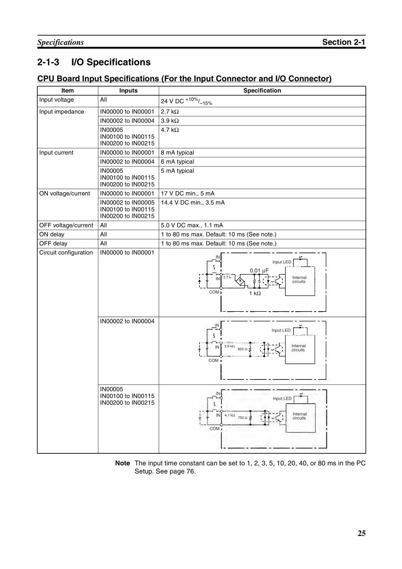
2-1-3 I/O Specifications
CPU Board Input Specifications (For the Input Connector and I/O Connector)
Note The input time constant can be set to 1, 2, 3, 5, 10, 20, 40, or 80 ms in the PCSetup. See page 76.
Item Inputs Specification
Input voltage All 24 V DC +10%/–15%
Input impedance IN00000 to IN00001 2.7 kΩIN00002 to IN00004 3.9 kΩIN00005IN00100 to IN00115IN00200 to IN00215
4.7 kΩ
Input current IN00000 to IN00001 8 mA typical
IN00002 to IN00004 6 mA typical
IN00005IN00100 to IN00115IN00200 to IN00215
5 mA typical
ON voltage/current IN00000 to IN00001 17 V DC min., 5 mA
IN00002 to IN00005IN00100 to IN00115IN00200 to IN00215
14.4 V DC min., 3.5 mA
OFF voltage/current All 5.0 V DC max., 1.1 mA
ON delay All 1 to 80 ms max. Default: 10 ms (See note.)
OFF delay All 1 to 80 ms max. Default: 10 ms (See note.)
Circuit configuration IN00000 to IN00001
IN00002 to IN00004
IN00005IN00100 to IN00115IN00200 to IN00215
1 kΩ
0.01 µF
IN
IN
COM
2.7 k Internal circuits
Input LED
IN
IN
COM
3.9 kΩ Internal circuits
Input LED
820 Ω
IN
IN
COM
4.7 kΩ Internal circuits
Input LED
750 Ω
26
Specifications Section 2-1
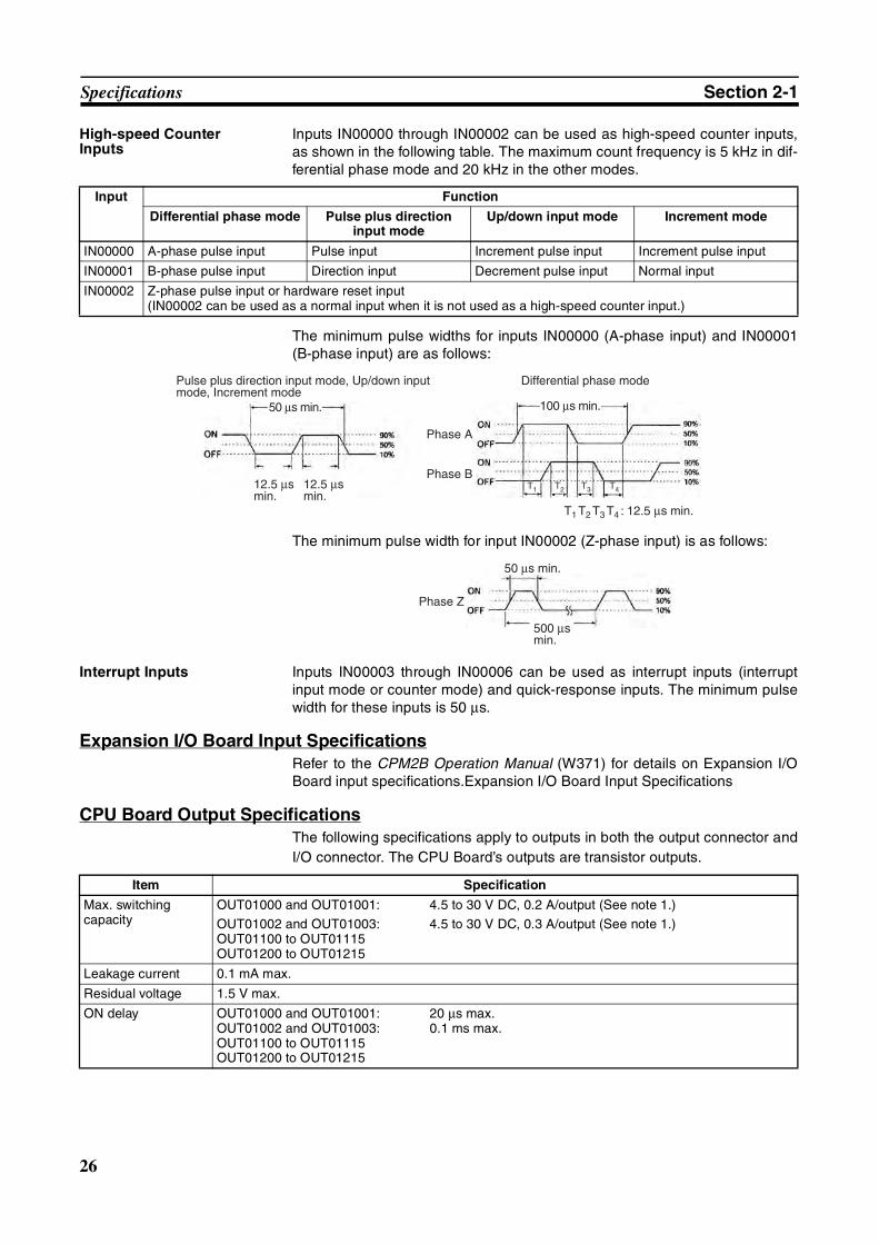
High-speed Counter Inputs
Inputs IN00000 through IN00002 can be used as high-speed counter inputs,as shown in the following table. The maximum count frequency is 5 kHz in dif-ferential phase mode and 20 kHz in the other modes.
The minimum pulse widths for inputs IN00000 (A-phase input) and IN00001(B-phase input) are as follows:
The minimum pulse width for input IN00002 (Z-phase input) is as follows:
Interrupt Inputs Inputs IN00003 through IN00006 can be used as interrupt inputs (interruptinput mode or counter mode) and quick-response inputs. The minimum pulsewidth for these inputs is 50 µs.
Expansion I/O Board Input SpecificationsRefer to the CPM2B Operation Manual (W371) for details on Expansion I/OBoard input specifications.Expansion I/O Board Input Specifications
CPU Board Output SpecificationsThe following specifications apply to outputs in both the output connector andI/O connector. The CPU Board’s outputs are transistor outputs.
Input Function
Differential phase mode Pulse plus direction input mode
Up/down input mode Increment mode
IN00000 A-phase pulse input Pulse input Increment pulse input Increment pulse input
IN00001 B-phase pulse input Direction input Decrement pulse input Normal input
IN00002 Z-phase pulse input or hardware reset input(IN00002 can be used as a normal input when it is not used as a high-speed counter input.)
100 µs min.
T1 T2 T3 T4 : 12.5 µs min.
Phase A
Phase B
50 µs min.
12.5 µs min.
Pulse plus direction input mode, Up/down input mode, Increment mode
Differential phase mode
12.5 µs min.
T1 T2 T3 T4
50 µs min.
500 µs min.
Phase Z
Item Specification
Max. switching capacity
OUT01000 and OUT01001: 4.5 to 30 V DC, 0.2 A/output (See note 1.)
OUT01002 and OUT01003: 4.5 to 30 V DC, 0.3 A/output (See note 1.)OUT01100 to OUT01115OUT01200 to OUT01215
Leakage current 0.1 mA max.
Residual voltage 1.5 V max.
ON delay OUT01000 and OUT01001: 20 µs max.OUT01002 and OUT01003: 0.1 ms max.OUT01100 to OUT01115OUT01200 to OUT01215
27
Specifications Section 2-1
Note 1. When using OUT01000 or OUT01001 for pulse outputs, connect a dummyresistor as required to bring the load current between 0.01 and 0.1 A. If theload current is below 0.01 A, the ON-to-OFF response time will be too longand high-speed pulses will not be output.
2. The specifications and circuit configuration are the same for the outputconnector’s outputs (OUT01100 to OUT01215).
!Caution Do not apply voltage in excess of the maximum switching capacity to an out-put terminal. It may result in damage to the product or fire.
OFF delay OUT01000 and OUT01001: 40 µs max. for 4.5 to 26.4 V, 10 to 100 mA0.1 ms max. for 4.5 to 30 V, 10 to 200 mA
OUT01002 and OUT01003: 1 ms max. for 4.5 to 30 V, 10 to 300 mA.OUT01100 to OUT01115OUT01200 to OUT01215
Fuse 1 fuse/output (cannot be replaced by user)
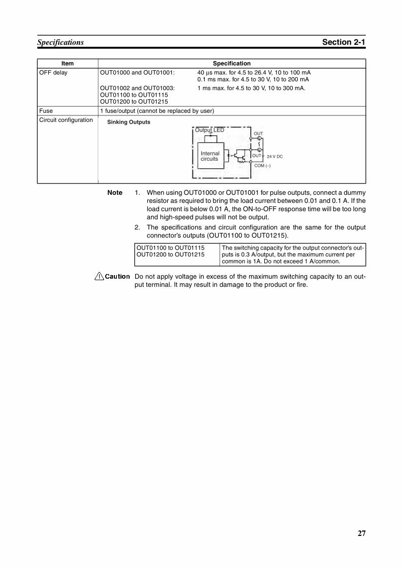
Circuit configuration
Item Specification
Sinking Outputs
COM (−)
Output LED
Internal circuits
OUT
OUT 24 V DC
OUT01100 to OUT01115OUT01200 to OUT01215
The switching capacity for the output connector’s out-puts is 0.3 A/output, but the maximum current per common is 1A. Do not exceed 1 A/common.
28
Board Components and their Functions Section 2-2
2-2 Board Components and their Functions
2-2-1 CPU Board ComponentsCPU Boards
CPU Board Component Descriptions
1,2,3... 1. Power Supply TerminalsConnect the power supply (24 V DC) to these terminals.
2. I/O Connector3. Input Connector
Connects the CPU Board to external input devices.4. Output Connector
Connects the CPU Board to external output devices.5. Status Indicators
These indicators show the operating status of the PC, as shown in the fol-lowing table.
IN000CH IN001CH IN002CH
OUT010CH OUT011CH OUT012CH
11 DeviceNet terminals
12 CompoBus/S terminals
5 Status indicators
9 Peripheral port
10 RS-232C port7 and 8 I/O indicators
2 I/O connector(6 inputs/4 outputs, interrupt inputs, high-speed counter inputs, pulse outputs)
15 Rotary switches
14 DIP switches
16 Battery holder
17 Battery low detection switch
1 Power supply terminals
13 Expansion I/O connector
3 Input connector (32 inputs)
18 Battery connector
6 DeviceNet Indicators
4 Output connector(32 outputs)
Indicator Status Meaning
PWR(green)
ON Power is being supplied to the PC.
OFF Power isn’t being supplied to the PC.
RUN(green)
ON The PC is operating in RUN or MONITOR mode.
OFF The PC is in PROGRAM mode or a fatal error has occurred.
ERR/ALM(red)
ON A fatal error has occurred. (PC operation stops.)
Flashing A non-fatal error has occurred. (PC operation continues.)
OFF Indicates normal operation.
COMM(yellow)
Flashing Data is being transferred via the communications port (peripheral or RS-232C).
OFF Data isn’t being transferred via communications port.
29
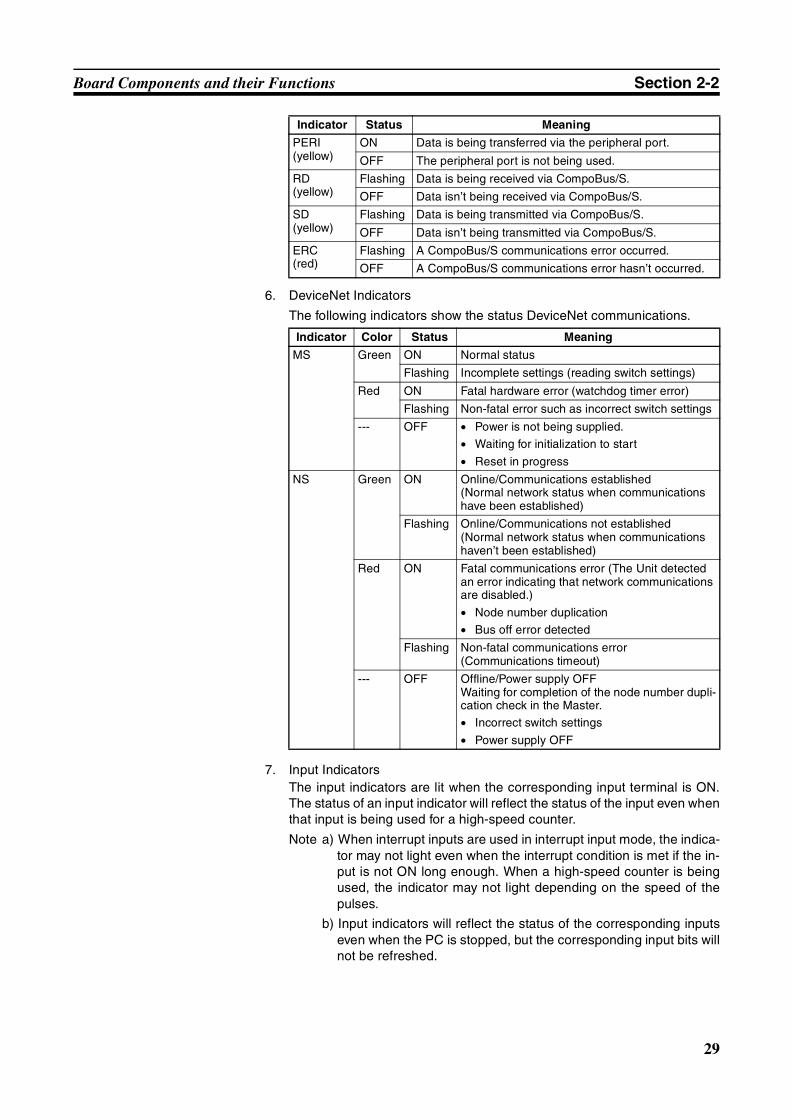
Board Components and their Functions Section 2-2
6. DeviceNet Indicators
The following indicators show the status DeviceNet communications.
7. Input IndicatorsThe input indicators are lit when the corresponding input terminal is ON.The status of an input indicator will reflect the status of the input even whenthat input is being used for a high-speed counter.
Note a) When interrupt inputs are used in interrupt input mode, the indica-tor may not light even when the interrupt condition is met if the in-put is not ON long enough. When a high-speed counter is beingused, the indicator may not light depending on the speed of thepulses.
b) Input indicators will reflect the status of the corresponding inputseven when the PC is stopped, but the corresponding input bits willnot be refreshed.
PERI(yellow)
ON Data is being transferred via the peripheral port.
OFF The peripheral port is not being used.
RD(yellow)
Flashing Data is being received via CompoBus/S.
OFF Data isn’t being received via CompoBus/S.
SD(yellow)
Flashing Data is being transmitted via CompoBus/S.
OFF Data isn’t being transmitted via CompoBus/S.
ERC(red)
Flashing A CompoBus/S communications error occurred.
OFF A CompoBus/S communications error hasn’t occurred.
Indicator Color Status Meaning
MS Green ON Normal status
Flashing Incomplete settings (reading switch settings)
Red ON Fatal hardware error (watchdog timer error)
Flashing Non-fatal error such as incorrect switch settings
--- OFF • Power is not being supplied.
• Waiting for initialization to start
• Reset in progress
NS Green ON Online/Communications established(Normal network status when communications have been established)
Flashing Online/Communications not established(Normal network status when communications haven’t been established)
Red ON Fatal communications error (The Unit detected an error indicating that network communications are disabled.)
• Node number duplication
• Bus off error detected
Flashing Non-fatal communications error(Communications timeout)
--- OFF Offline/Power supply OFFWaiting for completion of the node number dupli-cation check in the Master.
• Incorrect switch settings
• Power supply OFF
Indicator Status Meaning
30
Board Components and their Functions Section 2-2
8. Output Indicators
The output indicators are lit when the corresponding output terminal is ON.The indicators are lit during I/O refreshing. When an output is being usedas a pulse output, the corresponding will remain lit while pulses are beingoutput.
9. Peripheral Port
Connects the PC to a Programming Device (including Programming Con-soles), host computer, or standard external device.
10. RS-232C Port
Connects the PC to a Programming Device (excluding Programming Con-soles), host computer, Programmable Terminal, or standard external de-vice.
11. DeviceNet Terminals
12. CompoBus/S Terminals
13. Expansion I/O Connector
Connects the CPU Board to an Expansion I/O Board. Up to 3 Expansion I/O Boards can be connected to a CPU Board.
14. DIP Switch
The DIP switch settings determine the DeviceNet communications speedand control the communications settings for the communications port (pe-ripheral port and RS-232C port).
• DeviceNet communications speed
• RS-232C and Peripheral Port Settings
• Operating Mode at StartupPin 4 determines the operating mode at startup only if there isn’t a Pro-gramming Device connected to the peripheral port.
Note a) All four fins are set to OFF when the Board is shipped.
b) Always turn OFF the power supply before changing DIP Switchsettings. When changing pin settings, use an insulated tool thathas a fine tip such as a precision screwdriver with a plastic handle.
Pin 1 Pin 2 Speed Max. transmission line length (see note)
OFF OFF 125 kbps 500 m max.
ON OFF 250 kbps 250 m max.
OFF ON 500 kbps 100 m max.
ON ON Not used (invalid setting)
Pin 3 Effective port settings
OFF The ports operate according to the settings in the PC Setup.RS-232C port settings: DM 6645 to DM 6649Peripheral port settings: DM 6650 to DM 6654
ON The ports operate with the standard communications settings.
Programming Device connected
Startup mode withpin 4 OFF
Startup mode withpin 4 ON
None RUN mode PROGRAM mode
Programming Console Operating mode set on the Programming Console’s mode switch
Other device PROGRAM mode
ON
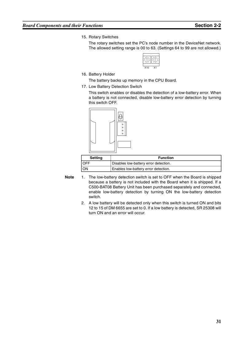
31
Board Components and their Functions Section 2-2
15. Rotary Switches
The rotary switches set the PC’s node number in the DeviceNet network.The allowed setting range is 00 to 63. (Settings 64 to 99 are not allowed.)
16. Battery Holder
The battery backs up memory in the CPU Board.
17. Low Battery Detection Switch
This switch enables or disables the detection of a low-battery error. Whena battery is not connected, disable low-battery error detection by turningthis switch OFF.
Note 1. The low-battery detection switch is set to OFF when the Board is shippedbecause a battery is not included with the Board when it is shipped. If aC500-BAT08 Battery Unit has been purchased separately and connected,enable low-battery detection by turning ON the low-battery detectionswitch.
2. A low battery will be detected only when this switch is turned ON and bits12 to 15 of DM 6655 are set to 0. If a low battery is detected, SR 25308 willturn ON and an error will occur.
Setting Function
OFF Disables low-battery error detection.
ON Enables low-battery error detection.
X10 X1
33
SECTION 3Installation and Wiring
This section provides information on installing and wiring a CPM2B-S PC. Be sure to follow the directions andprecautions in this section when installing the CPM2B-S in a panel or cabinet, wiring the power supply, or wiring I/O.
3-1 Design Precautions . . . . . . . . . . . . . . . . . . . . . . . . . . . . . . . . . . . . . . . . . . . . . 34
3-1-1 Power Supply Wiring . . . . . . . . . . . . . . . . . . . . . . . . . . . . . . . . . . . . 34
3-1-2 Power Supply Voltage . . . . . . . . . . . . . . . . . . . . . . . . . . . . . . . . . . . 34
3-1-3 Interlock and Limit Circuits . . . . . . . . . . . . . . . . . . . . . . . . . . . . . . . 34
3-2 Selecting an Installation Site . . . . . . . . . . . . . . . . . . . . . . . . . . . . . . . . . . . . . 35
3-2-1 Installation Site Conditions . . . . . . . . . . . . . . . . . . . . . . . . . . . . . . . 35
3-2-2 Panel/Cabinet Installation . . . . . . . . . . . . . . . . . . . . . . . . . . . . . . . . 35
3-3 Assembling the CPM2B-S Boards . . . . . . . . . . . . . . . . . . . . . . . . . . . . . . . . . 36
3-4 Installing the CPM2B-S . . . . . . . . . . . . . . . . . . . . . . . . . . . . . . . . . . . . . . . . . 38
3-5 Wiring and Connections . . . . . . . . . . . . . . . . . . . . . . . . . . . . . . . . . . . . . . . . . 39
3-5-1 Power Supply Wiring . . . . . . . . . . . . . . . . . . . . . . . . . . . . . . . . . . . . 40
3-5-2 I/O Wiring Procedures . . . . . . . . . . . . . . . . . . . . . . . . . . . . . . . . . . . 41
3-5-3 Wiring CompoBus/S Transmission Lines . . . . . . . . . . . . . . . . . . . . 51
3-5-4 Wiring DeviceNet Communications Cables . . . . . . . . . . . . . . . . . . 53
3-5-5 Connecting a Programming Device to the Peripheral Port . . . . . . . 54
3-5-6 Connecting to the RS-232C Port . . . . . . . . . . . . . . . . . . . . . . . . . . . 55
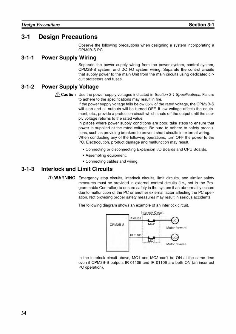
34
Design Precautions Section 3-1
3-1 Design PrecautionsObserve the following precautions when designing a system incorporating aCPM2B-S PC.
3-1-1 Power Supply WiringSeparate the power supply wiring from the power system, control system,CPM2B-S system, and DC I/O system wiring. Separate the control circuitsthat supply power to the main Unit from the main circuits using dedicated cir-cuit protectors and fuses.
3-1-2 Power Supply Voltage!Caution Use the power supply voltages indicated in Section 2-1 Specifications. Failure
to adhere to the specifications may result in fire.If the power supply voltage falls below 85% of the rated voltage, the CPM2B-Swill stop and all outputs will be turned OFF. If low voltage affects the equip-ment, etc., provide a protection circuit which shuts off the output until the sup-ply voltage returns to the rated value.In places where power supply conditions are poor, take steps to ensure thatpower is supplied at the rated voltage. Be sure to adhere to safety precau-tions, such as providing breakers to prevent short circuits in external wiring.When conducting any of the following operations, turn OFF the power to thePC. Electrocution, product damage and malfunction may result.
• Connecting or disconnecting Expansion I/O Boards and CPU Boards.
• Assembling equipment.
• Connecting cables and wiring.
3-1-3 Interlock and Limit Circuits
!WARNING Emergency stop circuits, interlock circuits, limit circuits, and similar safetymeasures must be provided in external control circuits (i.e., not in the Pro-grammable Controller) to ensure safety in the system if an abnormality occursdue to malfunction of the PC or another external factor affecting the PC oper-ation. Not providing proper safety measures may result in serious accidents.
The following diagram shows an example of an interlock circuit.
In the interlock circuit above, MC1 and MC2 can’t be ON at the same timeeven if CPM2B-S outputs IR 01105 and IR 01106 are both ON (an incorrectPC operation).
Interlock Circuit
Motor forward
Motor reverse
CPM2B-S
IR 01105
IR 01106
MC1
MC2
MC2
MC1
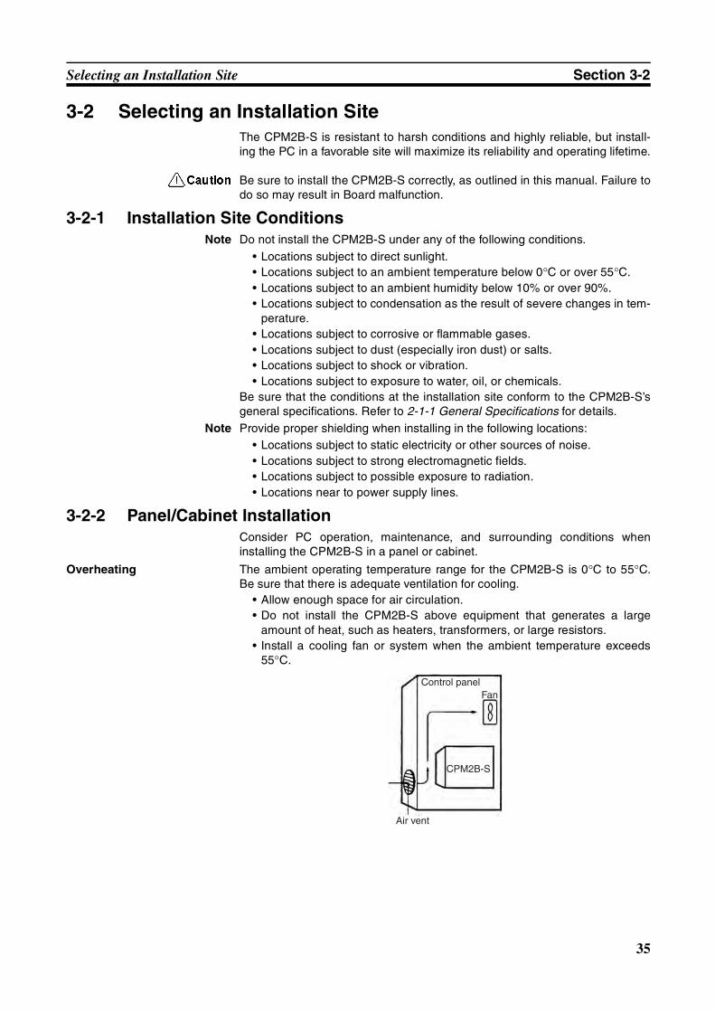
35
Selecting an Installation Site Section 3-2
3-2 Selecting an Installation SiteThe CPM2B-S is resistant to harsh conditions and highly reliable, but install-ing the PC in a favorable site will maximize its reliability and operating lifetime.
!Caution Be sure to install the CPM2B-S correctly, as outlined in this manual. Failure todo so may result in Board malfunction.
3-2-1 Installation Site ConditionsNote Do not install the CPM2B-S under any of the following conditions.
• Locations subject to direct sunlight.• Locations subject to an ambient temperature below 0°C or over 55°C.• Locations subject to an ambient humidity below 10% or over 90%.• Locations subject to condensation as the result of severe changes in tem-
perature.• Locations subject to corrosive or flammable gases.• Locations subject to dust (especially iron dust) or salts.• Locations subject to shock or vibration.• Locations subject to exposure to water, oil, or chemicals.
Be sure that the conditions at the installation site conform to the CPM2B-S’sgeneral specifications. Refer to 2-1-1 General Specifications for details.
Note Provide proper shielding when installing in the following locations:• Locations subject to static electricity or other sources of noise.• Locations subject to strong electromagnetic fields.• Locations subject to possible exposure to radiation.• Locations near to power supply lines.
3-2-2 Panel/Cabinet InstallationConsider PC operation, maintenance, and surrounding conditions wheninstalling the CPM2B-S in a panel or cabinet.
Overheating The ambient operating temperature range for the CPM2B-S is 0°C to 55°C.Be sure that there is adequate ventilation for cooling.
• Allow enough space for air circulation.• Do not install the CPM2B-S above equipment that generates a large
amount of heat, such as heaters, transformers, or large resistors.• Install a cooling fan or system when the ambient temperature exceeds
55°C.
Control panelFan
Air vent
CPM2B-S
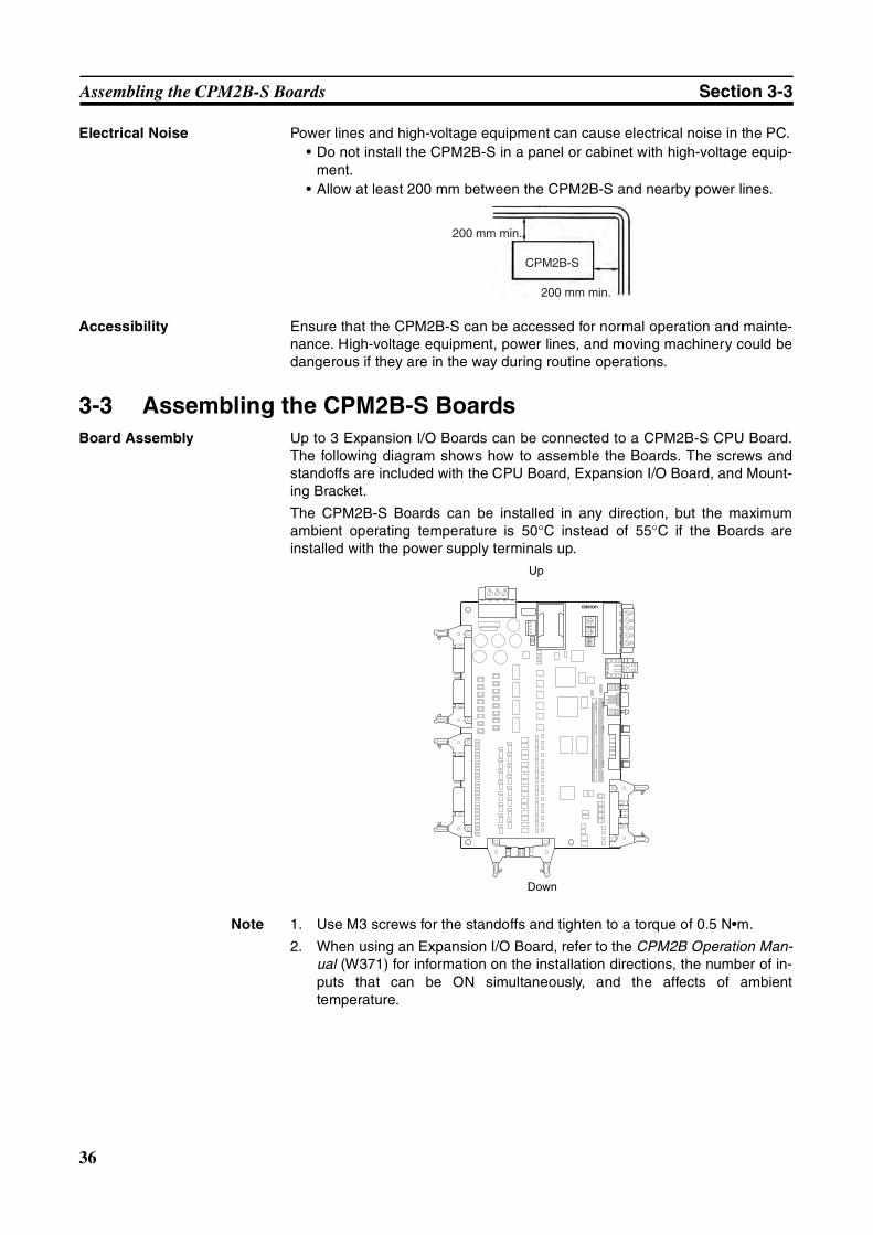
36
Assembling the CPM2B-S Boards Section 3-3
Electrical Noise Power lines and high-voltage equipment can cause electrical noise in the PC.• Do not install the CPM2B-S in a panel or cabinet with high-voltage equip-
ment.• Allow at least 200 mm between the CPM2B-S and nearby power lines.
Accessibility Ensure that the CPM2B-S can be accessed for normal operation and mainte-nance. High-voltage equipment, power lines, and moving machinery could bedangerous if they are in the way during routine operations.
3-3 Assembling the CPM2B-S BoardsBoard Assembly Up to 3 Expansion I/O Boards can be connected to a CPM2B-S CPU Board.
The following diagram shows how to assemble the Boards. The screws andstandoffs are included with the CPU Board, Expansion I/O Board, and Mount-ing Bracket.
The CPM2B-S Boards can be installed in any direction, but the maximumambient operating temperature is 50°C instead of 55°C if the Boards areinstalled with the power supply terminals up.
Note 1. Use M3 screws for the standoffs and tighten to a torque of 0.5 N•m.
2. When using an Expansion I/O Board, refer to the CPM2B Operation Man-ual (W371) for information on the installation directions, the number of in-puts that can be ON simultaneously, and the affects of ambienttemperature.
CPM2B-S
200 mm min.
200 mm min.
IN000C
HIN
001CH
IN002C
H
OU
T010CH
OU
T011CH
OU
T012CH
Up
Down
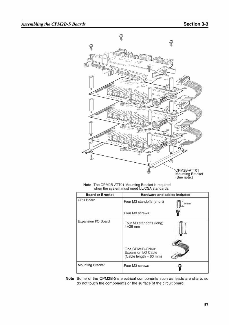
37
Assembling the CPM2B-S Boards Section 3-3
Note Some of the CPM2B-S’s electrical components such as leads are sharp, sodo not touch the components or the surface of the circuit board.
Board or Bracket Hardware and cables included
CPU Board
Expansion I/O Board
Mounting Bracket
15 14
15 14
15 14
Note The CPM2B-ATT01 Mounting Bracket is required when the system must meet UL/CSA standards.
CPM2B-ATT01 Mounting Bracket(See note.)
Four M3 standoffs (short)
Four M3 screws
10 mm
Four M3 standoffs (long)l =26 mm
One CPM2B-CN601 Expansion I/O Cable(Cable length = 60 mm)
l
Four M3 screws
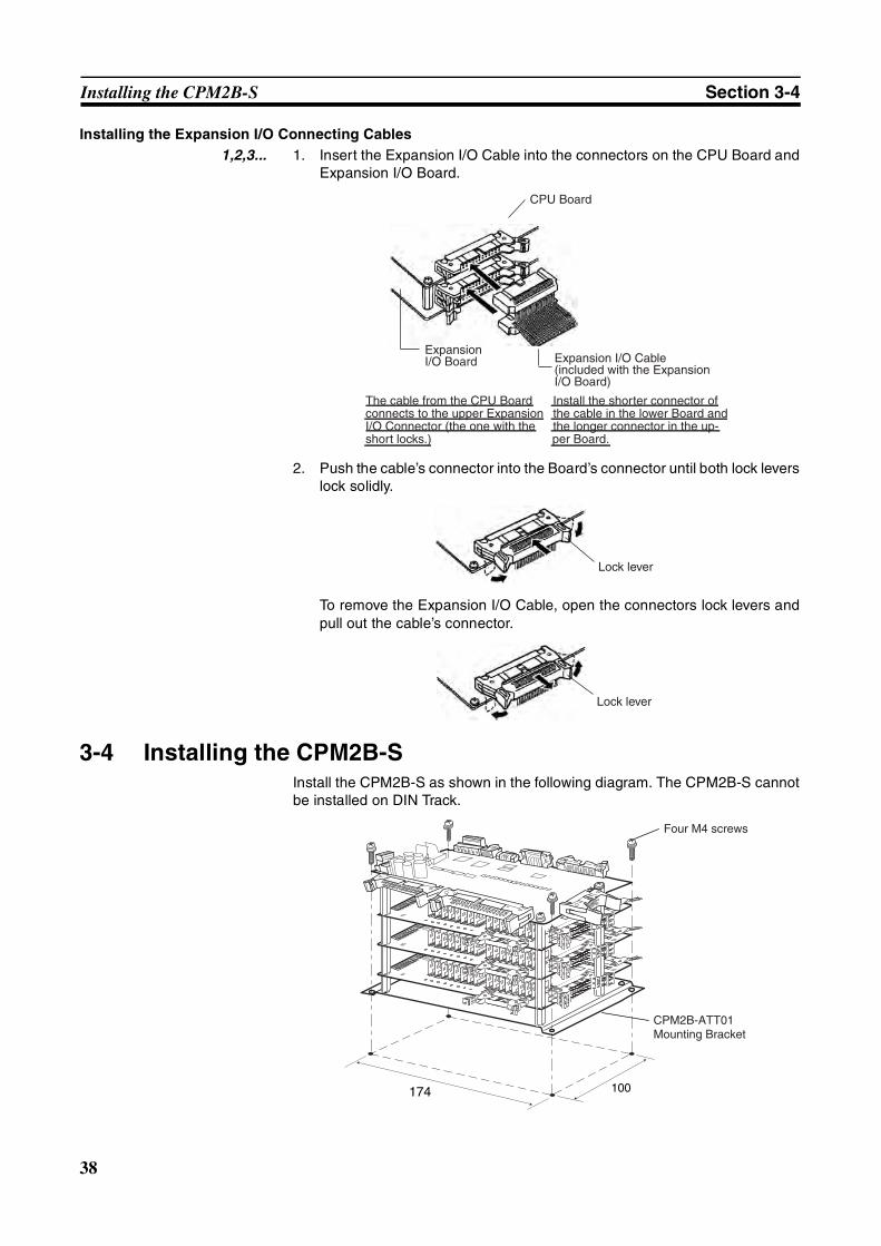
38
Installing the CPM2B-S Section 3-4
Installing the Expansion I/O Connecting Cables1,2,3... 1. Insert the Expansion I/O Cable into the connectors on the CPU Board and
Expansion I/O Board.
2. Push the cable’s connector into the Board’s connector until both lock leverslock solidly.
To remove the Expansion I/O Cable, open the connectors lock levers andpull out the cable’s connector.
3-4 Installing the CPM2B-SInstall the CPM2B-S as shown in the following diagram. The CPM2B-S cannotbe installed on DIN Track.
CPU Board
Expansion I/O Board Expansion I/O Cable
(included with the Expansion I/O Board)
connects to the upper Expansion I/O Connector (the one with the short locks.)
Install the shorter connector of the cable in the lower Board and the longer connector in the up-per Board.
The cable from the CPU Board
Lock lever
Lock lever
15 14
15 14
15 14
174 100
Four M4 screws
CPM2B-ATT01 Mounting Bracket
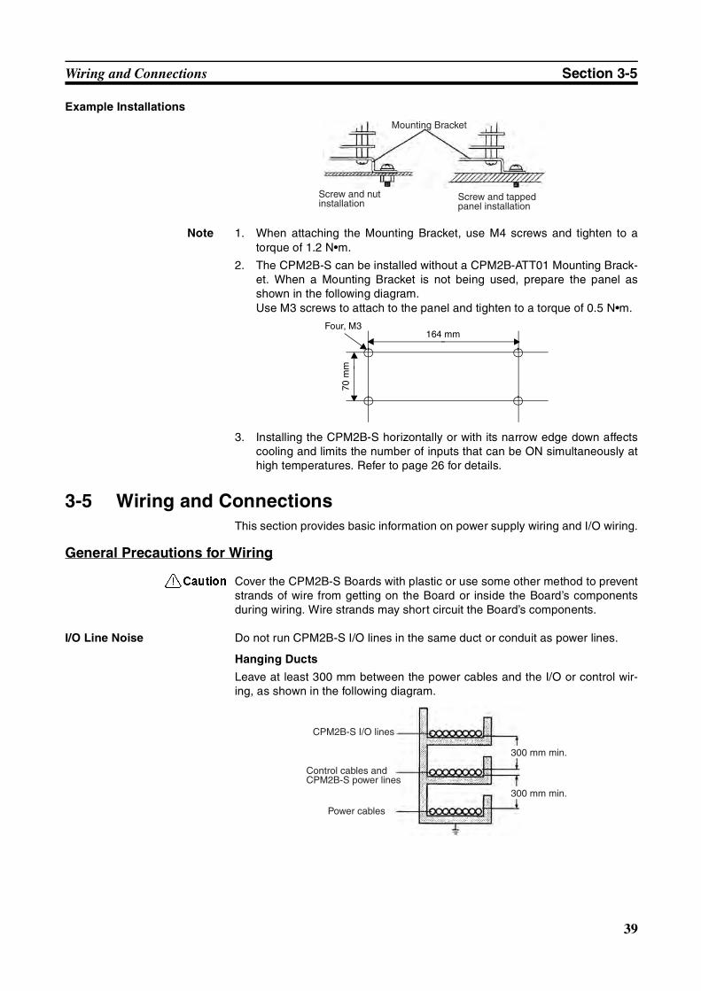
39
Wiring and Connections Section 3-5
Example Installations
Note 1. When attaching the Mounting Bracket, use M4 screws and tighten to atorque of 1.2 N•m.
2. The CPM2B-S can be installed without a CPM2B-ATT01 Mounting Brack-et. When a Mounting Bracket is not being used, prepare the panel asshown in the following diagram.Use M3 screws to attach to the panel and tighten to a torque of 0.5 N•m.
3. Installing the CPM2B-S horizontally or with its narrow edge down affectscooling and limits the number of inputs that can be ON simultaneously athigh temperatures. Refer to page 26 for details.
3-5 Wiring and ConnectionsThis section provides basic information on power supply wiring and I/O wiring.
General Precautions for Wiring
!Caution Cover the CPM2B-S Boards with plastic or use some other method to preventstrands of wire from getting on the Board or inside the Board’s componentsduring wiring. Wire strands may short circuit the Board’s components.
I/O Line Noise Do not run CPM2B-S I/O lines in the same duct or conduit as power lines.
Hanging Ducts
Leave at least 300 mm between the power cables and the I/O or control wir-ing, as shown in the following diagram.
Mounting Bracket
Screw and nut installation
Screw and tapped panel installation
164 mm70
mm
Four, M3
CPM2B-S I/O lines
Control cables and CPM2B-S power lines
Power cables
300 mm min.
300 mm min.
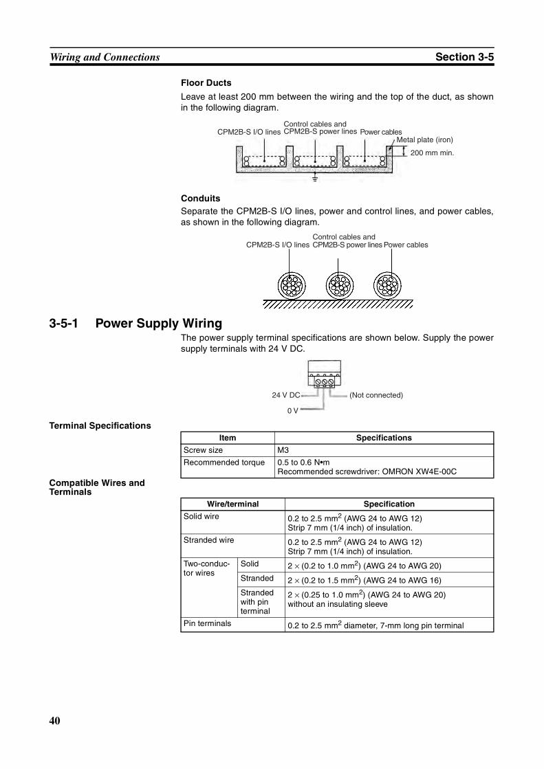
40
Wiring and Connections Section 3-5
Floor Ducts
Leave at least 200 mm between the wiring and the top of the duct, as shownin the following diagram.
ConduitsSeparate the CPM2B-S I/O lines, power and control lines, and power cables,as shown in the following diagram.
3-5-1 Power Supply WiringThe power supply terminal specifications are shown below. Supply the powersupply terminals with 24 V DC.
Terminal Specifications
Compatible Wires and Terminals
200 mm min.
Metal plate (iron)CPM2B-S I/O lines
Control cables and CPM2B-S power lines Power cables
CPM2B-S I/O linesControl cables and CPM2B-S power lines Power cables
24 V DC (Not connected)
0 V
Item Specifications
Screw size M3
Recommended torque 0.5 to 0.6 N•mRecommended screwdriver: OMRON XW4E-00C
Wire/terminal Specification
Solid wire 0.2 to 2.5 mm2 (AWG 24 to AWG 12)Strip 7 mm (1/4 inch) of insulation.
Stranded wire 0.2 to 2.5 mm2 (AWG 24 to AWG 12)Strip 7 mm (1/4 inch) of insulation.
Two-conduc-tor wires
Solid 2 × (0.2 to 1.0 mm2) (AWG 24 to AWG 20)
Stranded 2 × (0.2 to 1.5 mm2) (AWG 24 to AWG 16)
Stranded with pin terminal
2 × (0.25 to 1.0 mm2) (AWG 24 to AWG 20)without an insulating sleeve
Pin terminals 0.2 to 2.5 mm2 diameter, 7-mm long pin terminal
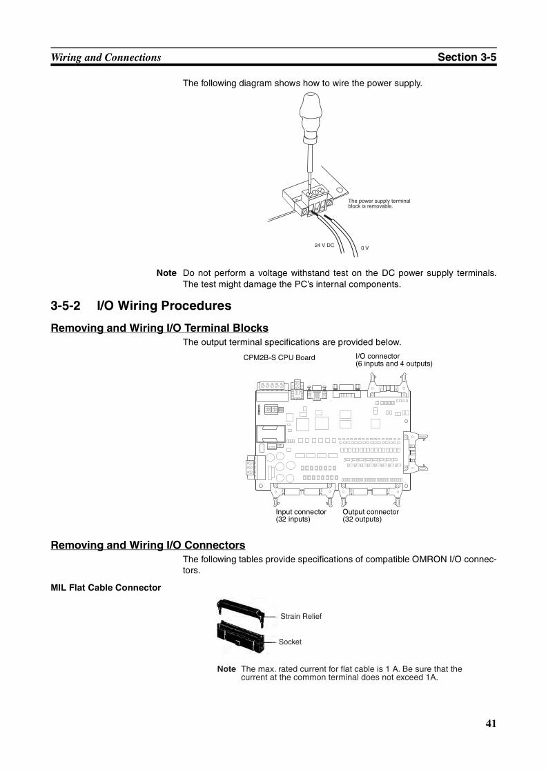
41
Wiring and Connections Section 3-5
The following diagram shows how to wire the power supply.
Note Do not perform a voltage withstand test on the DC power supply terminals.The test might damage the PC’s internal components.
3-5-2 I/O Wiring Procedures
Removing and Wiring I/O Terminal BlocksThe output terminal specifications are provided below.
Removing and Wiring I/O ConnectorsThe following tables provide specifications of compatible OMRON I/O connec-tors.
MIL Flat Cable Connector
The power supply terminal block is removable.
24 V DC 0 V
CPM2B-S CPU Board
Output connector (32 outputs)
I/O connector(6 inputs and 4 outputs)
Input connector (32 inputs)
Note The max. rated current for flat cable is 1 A. Be sure that the current at the common terminal does not exceed 1A.
Strain Relief
Socket
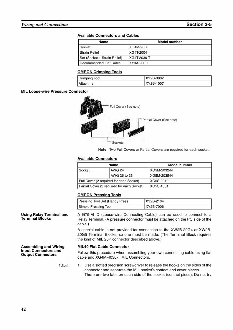
42
Wiring and Connections Section 3-5
Available Connectors and Cables
OMRON Crimping Tools
MIL Loose-wire Pressure Connector
Available Connectors
OMRON Pressing Tools
Using Relay Terminal and Terminal Blocks
A G79-A@C (Loose-wire Connecting Cable) can be used to connect to aRelay Terminal. (A pressure connector must be attached on the PC side of thecable.)
A special cable is not provided for connection to the XW2B-20G4 or XW2B-20G5 Terminal Blocks, so one must be made. (The Terminal Block requiresthe kind of MIL 20P connector described above.)
Assembling and Wiring Input Connectors and Output Connectors
MIL40 Flat Cable Connector
Follow this procedure when assembling your own connecting cable using flatcable and XG4M-4030-T MIL Connectors.
1,2,3... 1. Use a slotted precision screwdriver to release the hooks on the sides of theconnector and separate the MIL socket’s contact and cover pieces.There are two tabs on each side of the socket (contact piece). Do not try
Name Model number
Socket XG4M-2030
Strain Relief XG4T-2004
Set (Socket + Strain Relief) XG4T-2030-T
Recommended Flat Cable XY3A-200@
Crimping Tool XY2B-0002
Attachment XY2B-1007
Name Model number
Socket AWG 24 XG5M-2032-N
AWG 26 to 28 XG5M-2035-N
Full Cover (2 required for each Socket) XG5S-2012
Partial Cover (2 required for each Socket) XG5S-1001
Pressing Tool Set (Handy Press) XY2B-2104
Simple Pressing Tool XY2B-7006
Note Two Full Covers or Partial Covers are required for each socket.
Full Cover (See note)
Partial Cover (See note)
Sockets
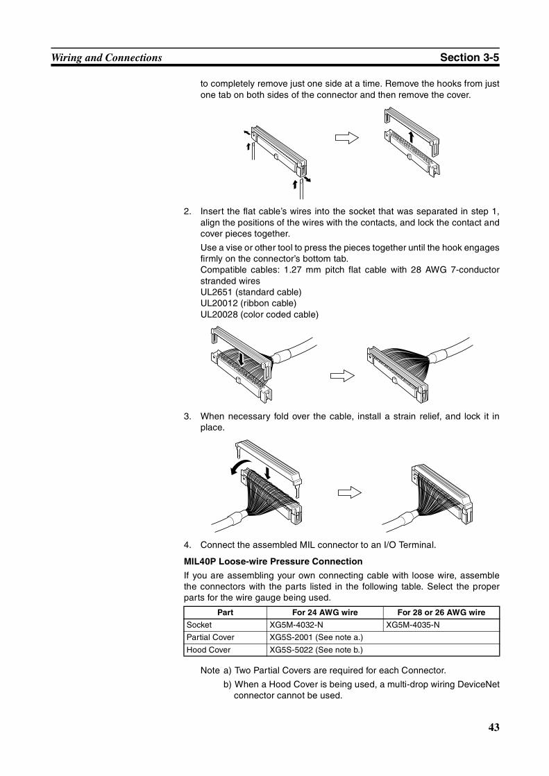
43
Wiring and Connections Section 3-5
to completely remove just one side at a time. Remove the hooks from justone tab on both sides of the connector and then remove the cover.
2. Insert the flat cable’s wires into the socket that was separated in step 1,align the positions of the wires with the contacts, and lock the contact andcover pieces together.
Use a vise or other tool to press the pieces together until the hook engagesfirmly on the connector’s bottom tab.Compatible cables: 1.27 mm pitch flat cable with 28 AWG 7-conductorstranded wiresUL2651 (standard cable)UL20012 (ribbon cable)UL20028 (color coded cable)
3. When necessary fold over the cable, install a strain relief, and lock it inplace.
4. Connect the assembled MIL connector to an I/O Terminal.
MIL40P Loose-wire Pressure Connection
If you are assembling your own connecting cable with loose wire, assemblethe connectors with the parts listed in the following table. Select the properparts for the wire gauge being used.
Note a) Two Partial Covers are required for each Connector.
b) When a Hood Cover is being used, a multi-drop wiring DeviceNetconnector cannot be used.
Part For 24 AWG wire For 28 or 26 AWG wire
Socket XG5M-4032-N XG5M-4035-N
Partial Cover XG5S-2001 (See note a.)
Hood Cover XG5S-5022 (See note b.)
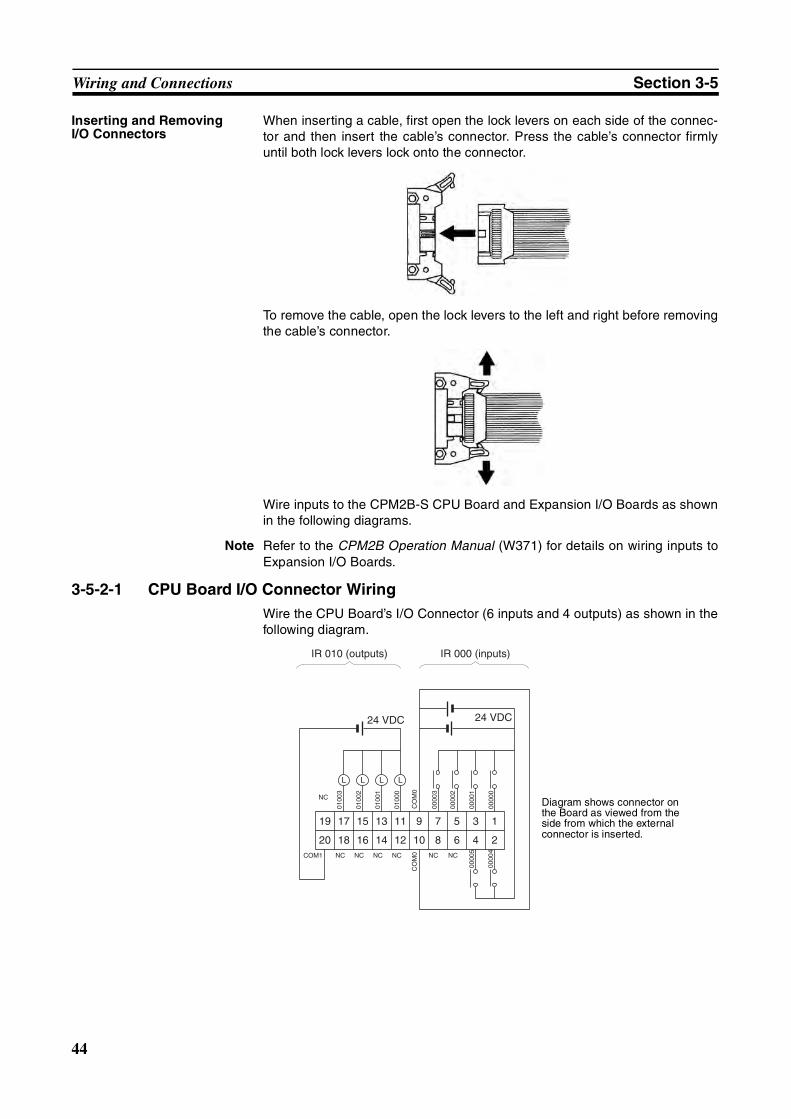
44
Wiring and Connections Section 3-5
Inserting and Removing I/O Connectors
When inserting a cable, first open the lock levers on each side of the connec-tor and then insert the cable’s connector. Press the cable’s connector firmlyuntil both lock levers lock onto the connector.
To remove the cable, open the lock levers to the left and right before removingthe cable’s connector.
Wire inputs to the CPM2B-S CPU Board and Expansion I/O Boards as shownin the following diagrams.
Note Refer to the CPM2B Operation Manual (W371) for details on wiring inputs toExpansion I/O Boards.
3-5-2-1 CPU Board I/O Connector WiringWire the CPU Board’s I/O Connector (6 inputs and 4 outputs) as shown in thefollowing diagram.
L L L L
19
20
17
18
15
16
13
14
11
12
9
10
7
8
5
6
3
4
1
2
24 VDC
IR 010 (outputs)
24 VDC
NC
COM1
CO
M0
0100
3
0100
2
0100
1
0100
0
0000
3
0000
2
0000
1
0000
0
CO
M0
0000
5
0000
4
NC NC NC NC NC NC
IR 000 (inputs)
Diagram shows connector on the Board as viewed from the side from which the external connector is inserted.
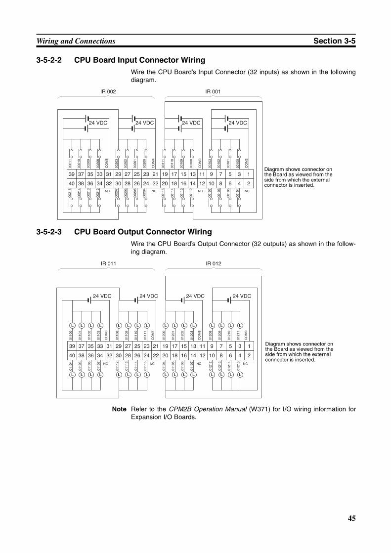
45
Wiring and Connections Section 3-5
3-5-2-2 CPU Board Input Connector WiringWire the CPU Board’s Input Connector (32 inputs) as shown in the followingdiagram.
3-5-2-3 CPU Board Output Connector WiringWire the CPU Board’s Output Connector (32 outputs) as shown in the follow-ing diagram.
Note Refer to the CPM2B Operation Manual (W371) for I/O wiring information forExpansion I/O Boards.
19
20
21
22
23
24
25
26
27
28
29
30
31
32
33
34
35
36
37
38
39
40
17
18
15
16
13
14
11
12
9
10
7
8
5
6
3
4
1
2
24 VDC
0010
3
0010
2
0010
1
0010
0
0010
7
0010
4
0010
5
0010
6
NC
CO
M2
24 VDC
0011
1
0011
0
0010
9
0010
8
0011
5
0011
2
0011
3
0011
4
NC
CO
M3
IR 001
24 VDC00
203
0020
2
0020
1
0020
0
0020
7
0020
4
0020
5
0020
6
NC
CO
M4
24 VDC
0021
1
0021
0
0020
9
0020
8
0021
5
0021
2
0021
3
0021
4
NC
CO
M5
IR 002
Diagram shows connector on the Board as viewed from the side from which the external connector is inserted.
19
20
21
22
23
24
25
26
27
28
29
30
31
32
33
34
35
36
37
38
39
40
17
18
15
16
13
14
11
12
9
10
7
8
5
6
3
4
1
2
IR 012IR 011
L
0110
0
L
0110
1
L
0110
2
L
L L L L
0110
3
CO
M6
0110
4
0110
5
0110
6
0110
7
24 VDC
NC
L
0110
8
L
0110
9
L
0111
0
L
L L L L
0111
1
CO
M7
0111
2
0111
3
0111
4
0111
5
24 VDC
NC
L
0120
0
L
0120
1
L
0120
2
L
L L L L
0120
3
CO
M8
0110
4
0110
5
0110
6
0110
7
24 VDC
NC
L
0120
8
L
0120
9
L
0121
0
L
L L L L
0121
1
CO
M9
0121
2
0121
3
0121
4
0121
5
24 VDC
NC
Diagram shows connector on the Board as viewed from the side from which the external connector is inserted.
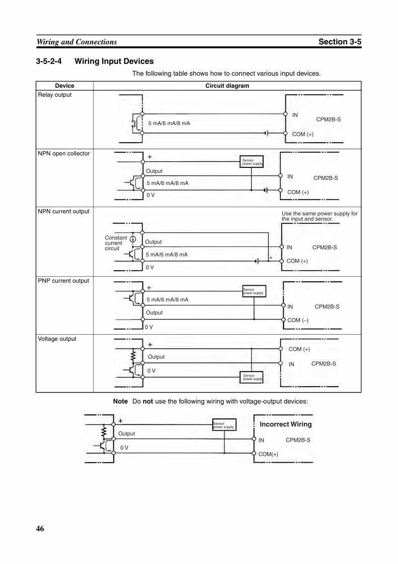
46
Wiring and Connections Section 3-5
3-5-2-4 Wiring Input DevicesThe following table shows how to connect various input devices.
Note Do not use the following wiring with voltage-output devices:
Device Circuit diagram
Relay output
NPN open collector
NPN current output
PNP current output
Voltage output
IN
COM (+)
5 mA/6 mA/8 mACPM2B-S
IN
COM (+)
Sensor power supply
Output
5 mA/6 mA/8 mACPM2B-S
0 V
Use the same power supply for the input and sensor.
CPM2B-SIN
COM (+)
Output
5 mA/6 mA/8 mA
0 V
Constant current circuit
+
Sensor power supply
COM (−)0 V
INOutput
5 mA/6 mA/8 mACPM2B-S
Sensor power supply
IN
COM (+)
0 V
OutputCPM2B-S
COM(+)
IN0 V
OutputCPM2B-S
Sensor power supply Incorrect Wiring
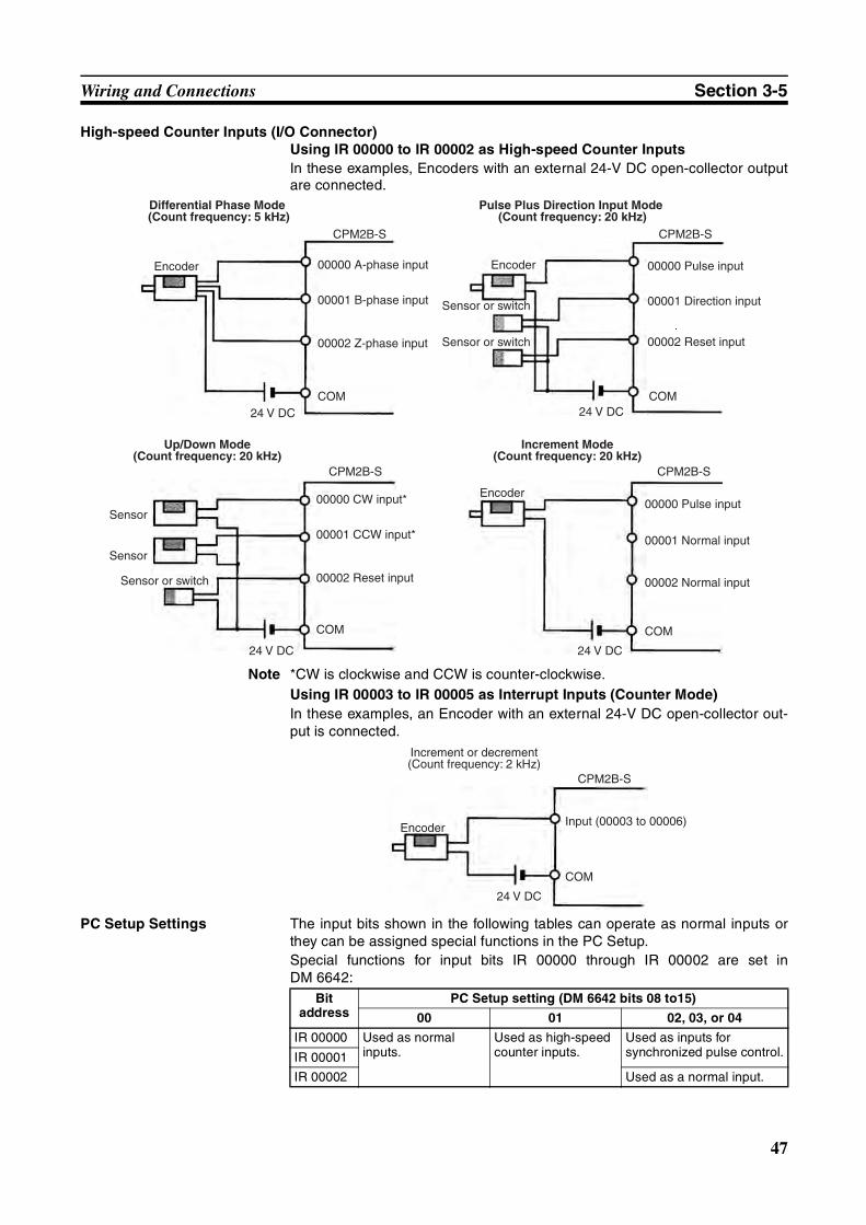
47
Wiring and Connections Section 3-5
High-speed Counter Inputs (I/O Connector)Using IR 00000 to IR 00002 as High-speed Counter InputsIn these examples, Encoders with an external 24-V DC open-collector outputare connected.
Note *CW is clockwise and CCW is counter-clockwise.Using IR 00003 to IR 00005 as Interrupt Inputs (Counter Mode)In these examples, an Encoder with an external 24-V DC open-collector out-put is connected.
PC Setup Settings The input bits shown in the following tables can operate as normal inputs orthey can be assigned special functions in the PC Setup.Special functions for input bits IR 00000 through IR 00002 are set inDM 6642:
Differential Phase Mode (Count frequency: 5 kHz)
Encoder
24 V DC
00000 A-phase input
00001 B-phase input
COM
00002 Z-phase input
Pulse Plus Direction Input Mode (Count frequency: 20 kHz)
Encoder
24 V DC
00000 Pulse input
00001 Direction input
COM
00002 Reset input
Sensor or switch
CPM2B-S CPM2B-S
Up/Down Mode(Count frequency: 20 kHz)
24 V DC
00000 CW input*
00001 CCW input*
COM
00002 Reset input
Increment Mode(Count frequency: 20 kHz)
Encoder
24 V DC
00000 Pulse input
00001 Normal input
COM
00002 Normal input
CPM2B-S CPM2B-S
Sensor
Sensor
Sensor or switch
Sensor or switch
Increment or decrement(Count frequency: 2 kHz)
Encoder
24 V DC
Input (00003 to 00006)
COM
CPM2B-S
Bit address
PC Setup setting (DM 6642 bits 08 to15)
00 01 02, 03, or 04
IR 00000 Used as normal inputs.
Used as high-speed counter inputs.
Used as inputs for synchronized pulse control.IR 00001
IR 00002 Used as a normal input.
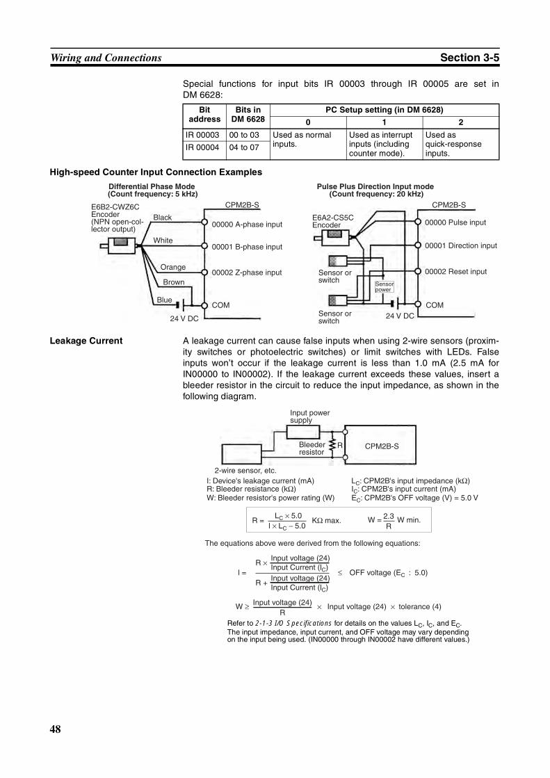
48
Wiring and Connections Section 3-5
Special functions for input bits IR 00003 through IR 00005 are set inDM 6628:
High-speed Counter Input Connection Examples
Leakage Current A leakage current can cause false inputs when using 2-wire sensors (proxim-ity switches or photoelectric switches) or limit switches with LEDs. Falseinputs won’t occur if the leakage current is less than 1.0 mA (2.5 mA forIN00000 to IN00002). If the leakage current exceeds these values, insert ableeder resistor in the circuit to reduce the input impedance, as shown in thefollowing diagram.
Bit address
Bits in DM 6628
PC Setup setting (in DM 6628)
0 1 2
IR 00003 00 to 03 Used as normal inputs.
Used as interrupt inputs (including counter mode).
Used as quick-response inputs.
IR 00004 04 to 07
Differential Phase Mode (Count frequency: 5 kHz)
E6B2-CWZ6C Encoder(NPN open-col-lector output)
24 V DC
00000 A-phase input
00001 B-phase input
COM
00002 Z-phase input
Pulse Plus Direction Input mode (Count frequency: 20 kHz)
E6A2-CS5C Encoder
24 V DC
00000 Pulse input
00001 Direction input
COM
00002 Reset inputSensor or switch
CPM2B-S CPM2B-S
Sensor or switch
Sensor power
Black
White
Orange
Brown
Blue
R CPM2B-S
Input power supply
Bleeder resistor
2-wire sensor, etc.I: Device's leakage current (mA)R: Bleeder resistance (kΩ)W: Bleeder resistor's power rating (W)
The equations above were derived from the following equations:
LC: CPM2B's input impedance (kΩ)IC: CPM2B's input current (mA)EC: CPM2B's OFF voltage (V) = 5.0 V
R = KΩ max.LC × 5.0
l × LC − 5.0W = W min.2.3
R
W ≥ × Input voltage (24) × tolerance (4)Input voltage (24)R
l = ≤ OFF voltage (EC : 5.0)R ×
R +
Input voltage (24)Input Current (lC)Input voltage (24)Input Current (lC)
Refer to 2-1-3 I/O Specifications for details on the values LC, IC, and EC.The input impedance, input current, and OFF voltage may vary depending on the input being used. (IN00000 through IN00002 have different values.)
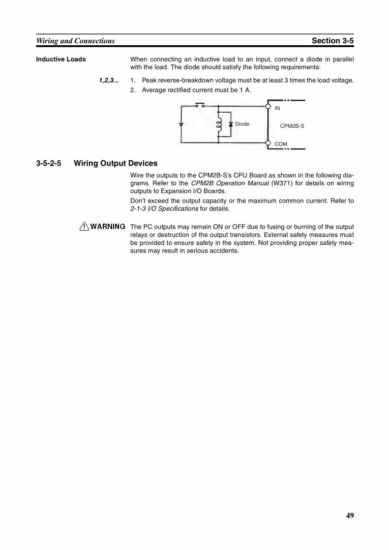
49
Wiring and Connections Section 3-5
Inductive Loads When connecting an inductive load to an input, connect a diode in parallelwith the load. The diode should satisfy the following requirements:
1,2,3... 1. Peak reverse-breakdown voltage must be at least 3 times the load voltage.
2. Average rectified current must be 1 A.
3-5-2-5 Wiring Output DevicesWire the outputs to the CPM2B-S’s CPU Board as shown in the following dia-grams. Refer to the CPM2B Operation Manual (W371) for details on wiringoutputs to Expansion I/O Boards.
Don’t exceed the output capacity or the maximum common current. Refer to2-1-3 I/O Specifications for details.
!WARNING The PC outputs may remain ON or OFF due to fusing or burning of the outputrelays or destruction of the output transistors. External safety measures mustbe provided to ensure safety in the system. Not providing proper safety mea-sures may result in serious accidents.
IN
COM
CPM2B-SDiode
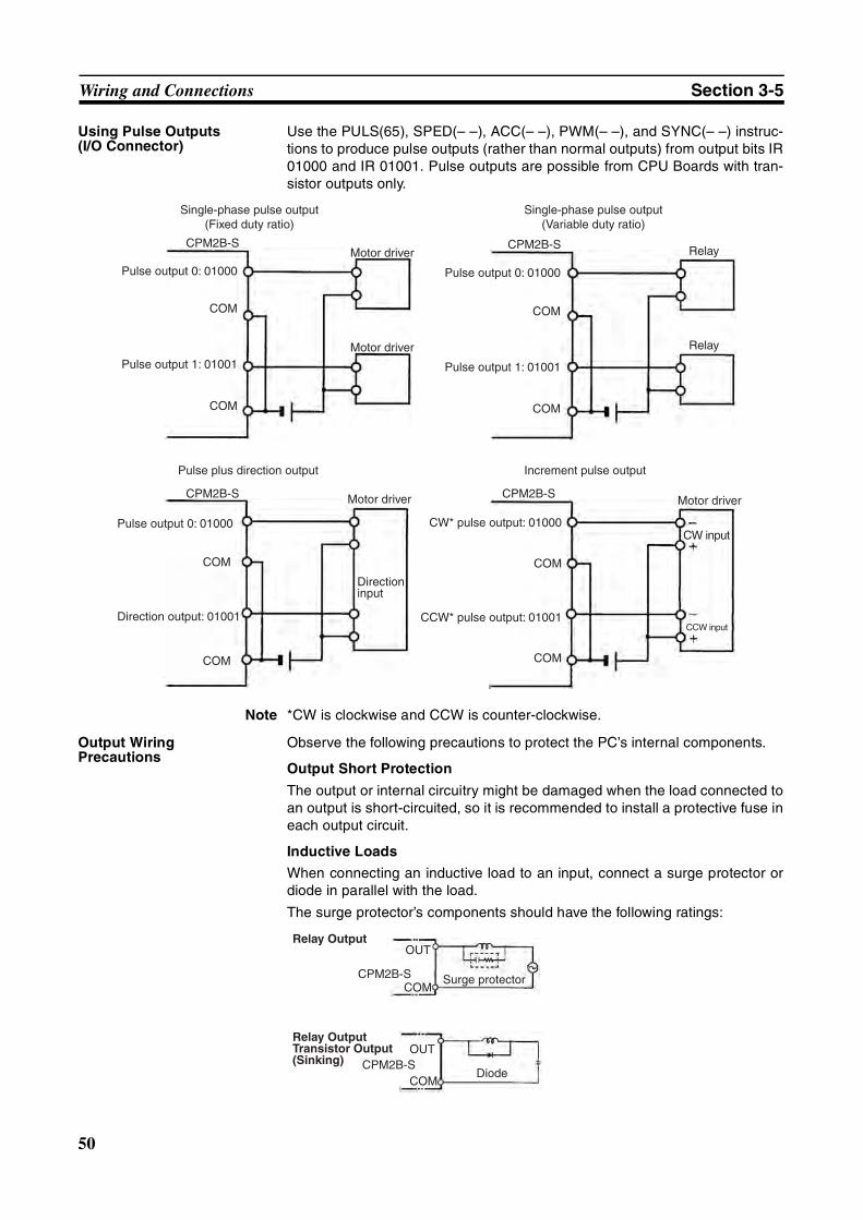
50
Wiring and Connections Section 3-5
Using Pulse Outputs(I/O Connector)
Use the PULS(65), SPED(– –), ACC(– –), PWM(– –), and SYNC(– –) instruc-tions to produce pulse outputs (rather than normal outputs) from output bits IR01000 and IR 01001. Pulse outputs are possible from CPU Boards with tran-sistor outputs only.
Note *CW is clockwise and CCW is counter-clockwise.
Output Wiring Precautions
Observe the following precautions to protect the PC’s internal components.
Output Short Protection
The output or internal circuitry might be damaged when the load connected toan output is short-circuited, so it is recommended to install a protective fuse ineach output circuit.
Inductive Loads
When connecting an inductive load to an input, connect a surge protector ordiode in parallel with the load.
The surge protector’s components should have the following ratings:
CPM2B-S
Single-phase pulse output(Fixed duty ratio)
Motor driver
Pulse output 0: 01000
CPM2B-S
Pulse output 1: 01001
COM
Motor driver
Single-phase pulse output(Variable duty ratio)
Relay
Pulse output 0: 01000
CPM2B-S
Pulse output 1: 01001
COM
Relay
Pulse plus direction output
Motor driver
Pulse output 0: 01000
CPM2B-S
Direction output: 01001
COM
Directioninput
Increment pulse output
Motor driver
CW* pulse output: 01000
CCW* pulse output: 01001
COM
CW input
CCW input
COM COM
COM COM
OUT
COMCPM2B-S Surge protector
Relay Output
OUT
COMCPM2B-S
Diode
Relay OutputTransistor Output(Sinking)
51
Wiring and Connections Section 3-5
The diode should satisfy the following requirements:
Peak reverse-breakdown voltage must be at least 3 times the load voltage.Average rectified current must be 1 A.
Inrush Current Considerations
When a relay or transistor output is used to switch a load with a high inrushcurrent such as an incandescent lamp, suppress the inrush current as shownbelow.
Fuse Insertion
The CPM2B-S with transistor output may burn if the load is short-circuited,therefore, insert a protective fuse in series with the load.
3-5-3 Wiring CompoBus/S Transmission LinesUse special flat cable or VCTF cable for the transmission lines that connectthe nodes in the CompoBus/S I/O Link. (Special flat cables and VCTF cablescannot be combined in the same system.)
Use the following procedure to wire the CompoBus/S communications cables.
1,2,3... 1. Strip off the length of wire insulation recommended for the crimp connec-tors being used and tightly twist the bare wire strands together.
Note When VCTF cable is being used, cover the end of the cable sheathing withelectrical tape or heat-shrink tubing as shown in the following diagram.
2. Crimp pin terminals on the stripped ends of the communications cable andsecure the terminal and wire with electrical tape or heat-shrink tubing.
Note a) We recommend the following pin terminals.
R
R
Countermeasure 1
Providing a dark current of approx. one-third of the rated value through an incandescent lamp
Countermeasure 2
Providing a limiting resistor
OUT
COM
OUT
COM
Name Model number Specifications
Flat cable XB1T-W10 4-core flat cable, 0.75 mm2
VCTF cable --- 2-core VCTF, 0.75 × 20
Secure the cable sheathing with electrical tape or heat-shrink tubing.
Weidmüller 046290 Sleeve
Signal wire
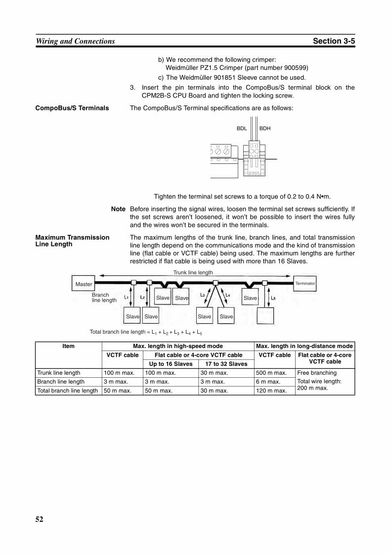
52
Wiring and Connections Section 3-5
b) We recommend the following crimper:Weidmüller PZ1.5 Crimper (part number 900599)
c) The Weidmüller 901851 Sleeve cannot be used.
3. Insert the pin terminals into the CompoBus/S terminal block on theCPM2B-S CPU Board and tighten the locking screw.
CompoBus/S Terminals The CompoBus/S Terminal specifications are as follows:
Tighten the terminal set screws to a torque of 0.2 to 0.4 N•m.
Note Before inserting the signal wires, loosen the terminal set screws sufficiently. Ifthe set screws aren’t loosened, it won’t be possible to insert the wires fullyand the wires won’t be secured in the terminals.
Maximum Transmission Line Length
The maximum lengths of the trunk line, branch lines, and total transmissionline length depend on the communications mode and the kind of transmissionline (flat cable or VCTF cable) being used. The maximum lengths are furtherrestricted if flat cable is being used with more than 16 Slaves.
BDL BDH
Item Max. length in high-speed mode Max. length in long-distance mode
VCTF cable Flat cable or 4-core VCTF cable VCTF cable Flat cable or 4-core VCTF cableUp to 16 Slaves 17 to 32 Slaves
Trunk line length 100 m max. 100 m max. 30 m max. 500 m max. Free branching
Total wire length:200 m max.
Branch line length 3 m max. 3 m max. 3 m max. 6 m max.
Total branch line length 50 m max. 50 m max. 30 m max. 120 m max.
Master
Branch line length
Slave Slave
Slave Slave
Slave Slave
Slave
Terminator
Trunk line length
Total branch line length = L1 + L2 + L3 + L4 + L5
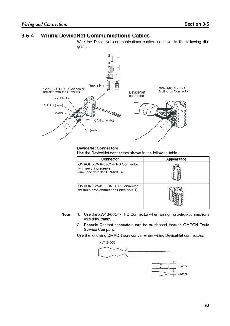
53
Wiring and Connections Section 3-5
3-5-4 Wiring DeviceNet Communications CablesWire the DeviceNet communications cables as shown in the following dia-gram.
DeviceNet ConnectorsUse the DeviceNet connectors shown in the following table.
Note 1. Use the XW4B-05C4-T1-D Connector when wiring multi-drop connectionswith thick cable.
2. Phoenix Contact connectors can be purchased through OMRON TsufoService Company.
Use the following OMRON screwdriver when wiring DeviceNet connectors.
XW4B-05C1-H1-D Connector included with the CPM2B-S
V+ (black)
CAN H (blue)
Shield
V
(red)
CAN L (white)
XW4B-05C4-TF-D Multi-drop Connector
DeviceNet
DeviceNet connector
Connector Appearance
OMRON XW4B-05C1-H1-D Connector with securing screws(included with the CPM2B-S)
OMRON XW4B-05C4-TF-D Connector for multi-drop connections (see note 1)
XW4Z-00C
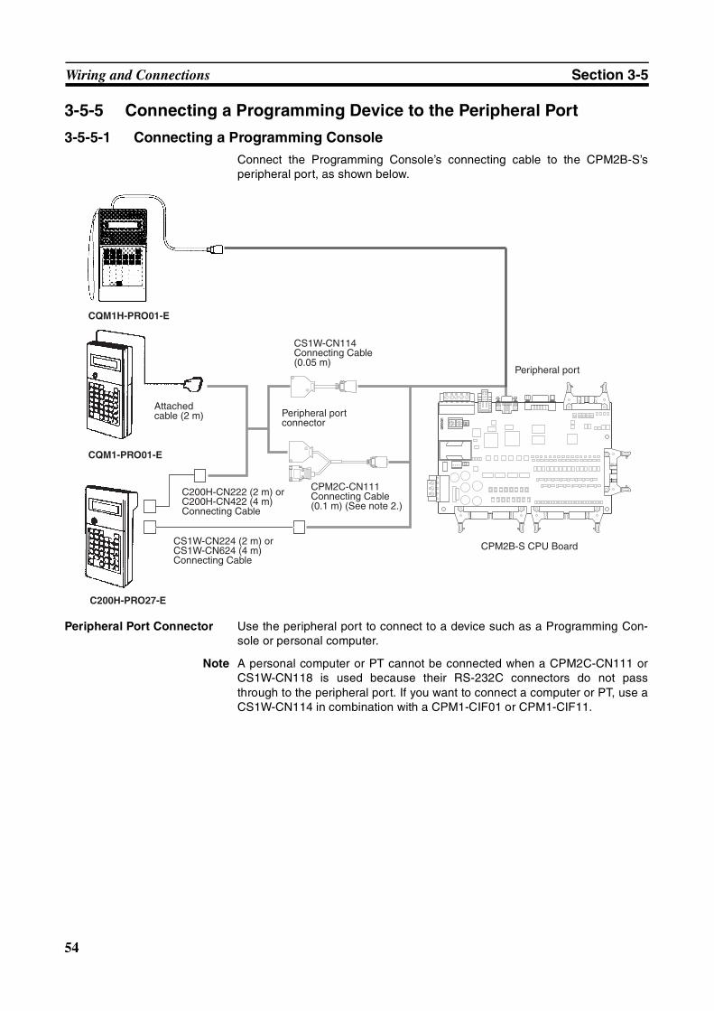
54
Wiring and Connections Section 3-5
3-5-5 Connecting a Programming Device to the Peripheral Port
3-5-5-1 Connecting a Programming ConsoleConnect the Programming Console’s connecting cable to the CPM2B-S’speripheral port, as shown below.
Peripheral Port Connector Use the peripheral port to connect to a device such as a Programming Con-sole or personal computer.
Note A personal computer or PT cannot be connected when a CPM2C-CN111 orCS1W-CN118 is used because their RS-232C connectors do not passthrough to the peripheral port. If you want to connect a computer or PT, use aCS1W-CN114 in combination with a CPM1-CIF01 or CPM1-CIF11.
Peripheral port
CPM2C-CN111 Connecting Cable(0.1 m) (See note 2.)
CS1W-CN114 Connecting Cable (0.05 m)
CQM1-PRO01-E
CS1W-CN224 (2 m) or CS1W-CN624 (4 m) Connecting Cable
CPM2B-S CPU Board
C200H-PRO27-E
C200H-CN222 (2 m) or C200H-CN422 (4 m) Connecting Cable
Attached cable (2 m) Peripheral port
connector
CQM1H-PRO01-E
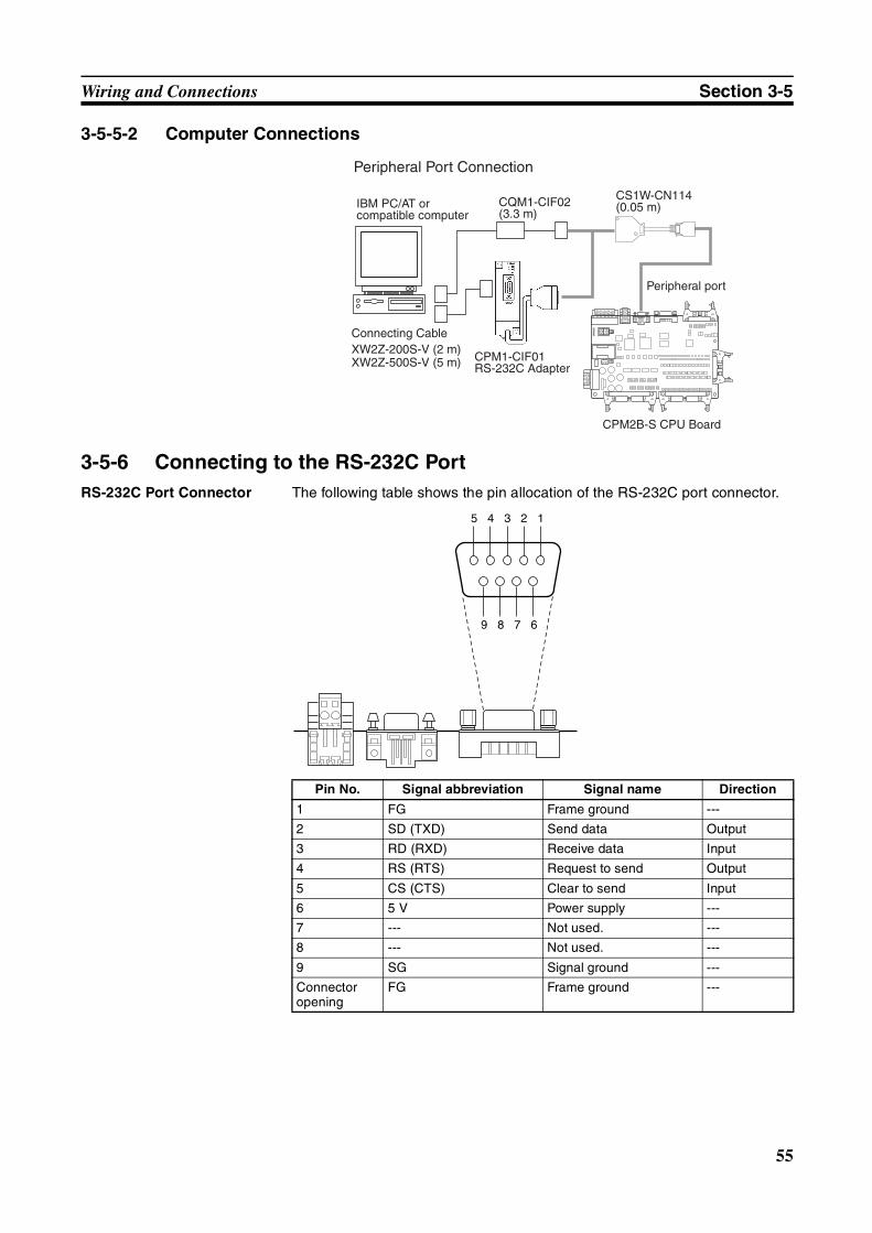
55
Wiring and Connections Section 3-5
3-5-5-2 Computer Connections
3-5-6 Connecting to the RS-232C PortRS-232C Port Connector The following table shows the pin allocation of the RS-232C port connector.
Peripheral port
CPM2B-S CPU Board
Connecting CableXW2Z-200S-V (2 m)XW2Z-500S-V (5 m)
IBM PC/AT or compatible computer
Peripheral Port Connection
CS1W-CN114 (0.05 m)CQM1-CIF02
(3.3 m)
CPM1-CIF01 RS-232C Adapter
Pin No. Signal abbreviation Signal name Direction
1 FG Frame ground ---
2 SD (TXD) Send data Output
3 RD (RXD) Receive data Input
4 RS (RTS) Request to send Output
5 CS (CTS) Clear to send Input
6 5 V Power supply ---
7 --- Not used. ---
8 --- Not used. ---
9 SG Signal ground ---
Connector opening
FG Frame ground ---
5 4 3 2 1
9 8 7 6
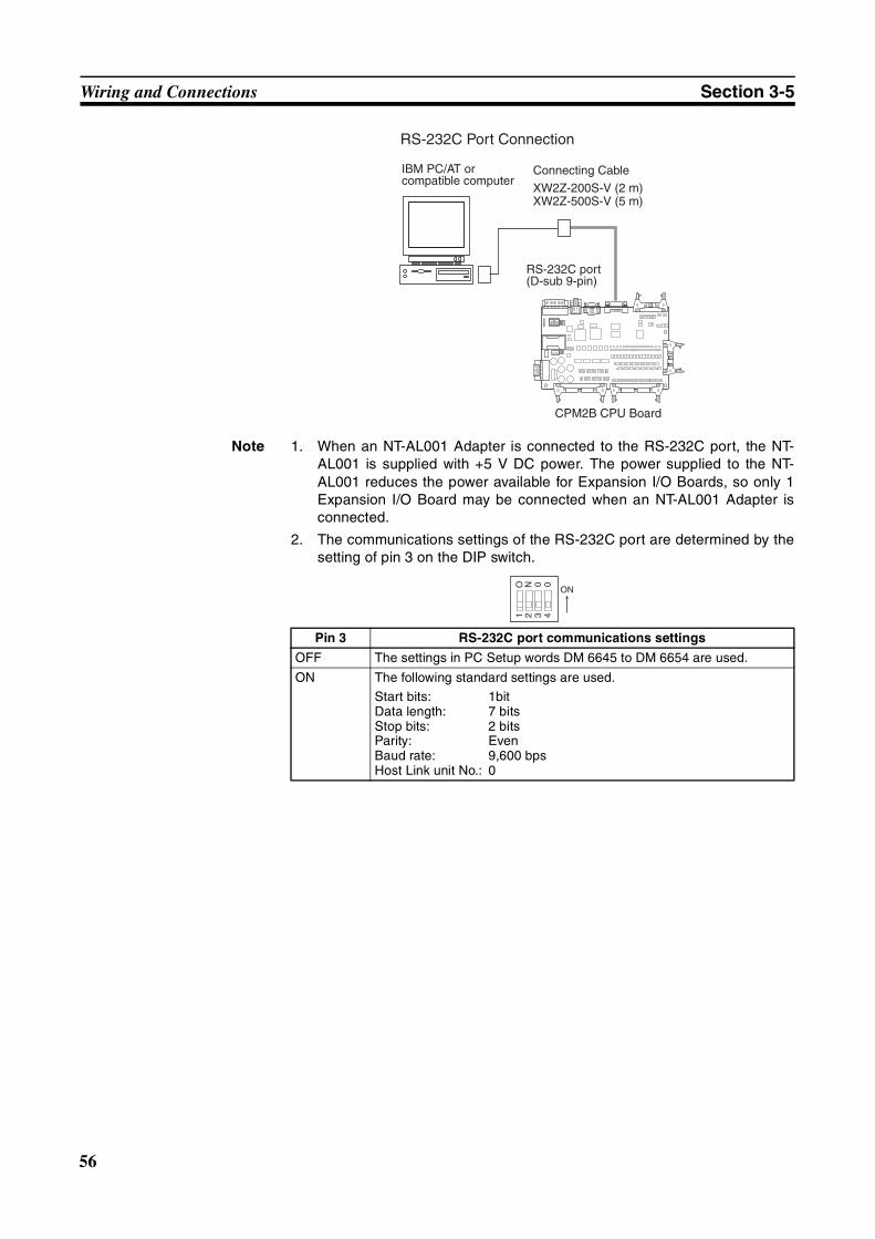
56
Wiring and Connections Section 3-5
Note 1. When an NT-AL001 Adapter is connected to the RS-232C port, the NT-AL001 is supplied with +5 V DC power. The power supplied to the NT-AL001 reduces the power available for Expansion I/O Boards, so only 1Expansion I/O Board may be connected when an NT-AL001 Adapter isconnected.
2. The communications settings of the RS-232C port are determined by thesetting of pin 3 on the DIP switch.
RS-232C port (D-sub 9-pin)
CPM2B CPU Board
Connecting Cable
XW2Z-200S-V (2 m)XW2Z-500S-V (5 m)
IBM PC/AT or compatible computer
RS-232C Port Connection
Pin 3 RS-232C port communications settings
OFF The settings in PC Setup words DM 6645 to DM 6654 are used.
ON The following standard settings are used.
Start bits: 1bitData length: 7 bitsStop bits: 2 bitsParity: EvenBaud rate: 9,600 bpsHost Link unit No.: 0
ON
57
SECTION 4Memory Areas
This section describes the structure of the PC memory areas and explains how to use them.
4-1 Introduction . . . . . . . . . . . . . . . . . . . . . . . . . . . . . . . . . . . . . . . . . . . . . . . . . . 58
4-1-1 Functions . . . . . . . . . . . . . . . . . . . . . . . . . . . . . . . . . . . . . . . . . . . . . 59
4-1-2 I/O Memory Area Attributes . . . . . . . . . . . . . . . . . . . . . . . . . . . . . . 62
4-2 I/O Allocation for CPM2B-S PCs . . . . . . . . . . . . . . . . . . . . . . . . . . . . . . . . . 63
4-3 I/O Allocation to CompoBus/S Slaves . . . . . . . . . . . . . . . . . . . . . . . . . . . . . . 65
4-4 SR Area . . . . . . . . . . . . . . . . . . . . . . . . . . . . . . . . . . . . . . . . . . . . . . . . . . . . . 66
4-5 AR Area . . . . . . . . . . . . . . . . . . . . . . . . . . . . . . . . . . . . . . . . . . . . . . . . . . . . . 69
4-6 PC Setup . . . . . . . . . . . . . . . . . . . . . . . . . . . . . . . . . . . . . . . . . . . . . . . . . . . . . 73
4-6-1 Overview . . . . . . . . . . . . . . . . . . . . . . . . . . . . . . . . . . . . . . . . . . . . . 73
4-6-2 PC Setup Settings. . . . . . . . . . . . . . . . . . . . . . . . . . . . . . . . . . . . . . . 74
4-7 Basic PC Operation and I/O Processes. . . . . . . . . . . . . . . . . . . . . . . . . . . . . . 79
4-7-1 Startup Mode . . . . . . . . . . . . . . . . . . . . . . . . . . . . . . . . . . . . . . . . . . 79
4-7-2 Hold Bit Status . . . . . . . . . . . . . . . . . . . . . . . . . . . . . . . . . . . . . . . . . 80
4-7-3 Program Memory Write-protection . . . . . . . . . . . . . . . . . . . . . . . . . 80
4-7-4 RS-232C Port Servicing Time . . . . . . . . . . . . . . . . . . . . . . . . . . . . . 81
4-7-5 Peripheral Port Servicing Time . . . . . . . . . . . . . . . . . . . . . . . . . . . . 81
4-7-6 Cycle Monitor Time . . . . . . . . . . . . . . . . . . . . . . . . . . . . . . . . . . . . . 81
4-7-7 Minimum Cycle Time . . . . . . . . . . . . . . . . . . . . . . . . . . . . . . . . . . . 82
4-7-8 Input Time Constants . . . . . . . . . . . . . . . . . . . . . . . . . . . . . . . . . . . . 82
4-7-9 Error Detection and Error Log Settings . . . . . . . . . . . . . . . . . . . . . . 83
4-8 Error Log . . . . . . . . . . . . . . . . . . . . . . . . . . . . . . . . . . . . . . . . . . . . . . . . . . . . 84
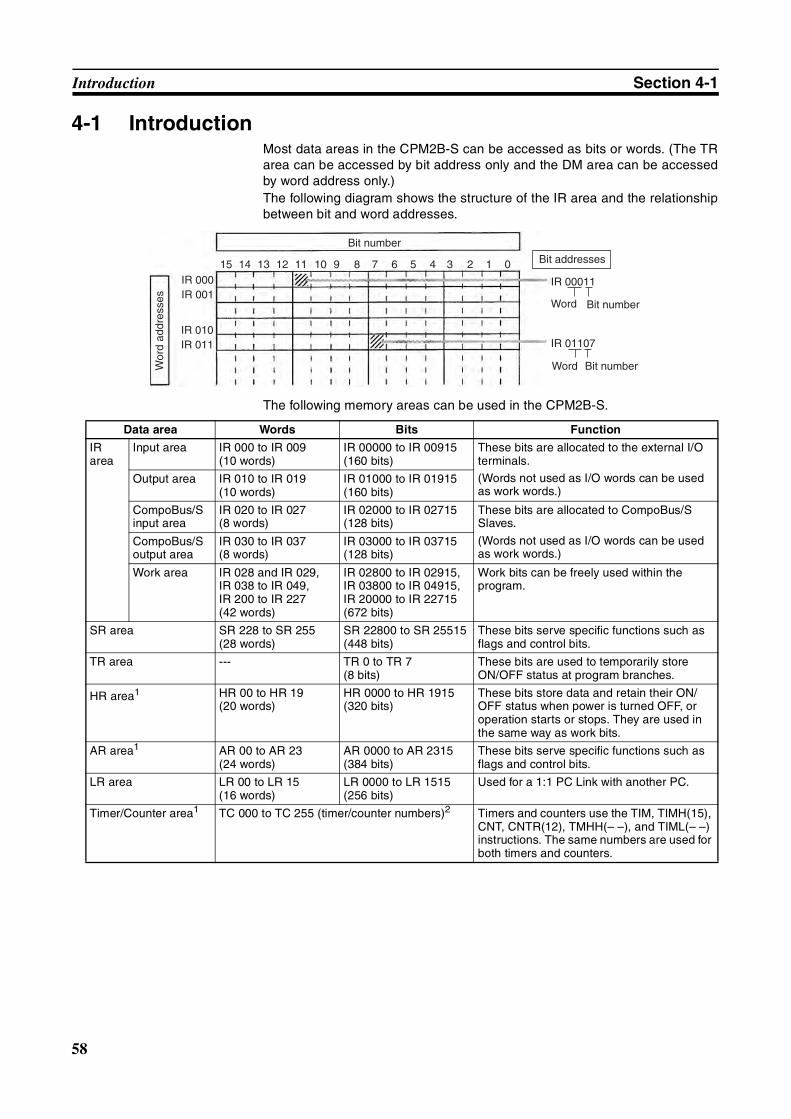
58
Introduction Section 4-1
4-1 IntroductionMost data areas in the CPM2B-S can be accessed as bits or words. (The TRarea can be accessed by bit address only and the DM area can be accessedby word address only.)The following diagram shows the structure of the IR area and the relationshipbetween bit and word addresses.
The following memory areas can be used in the CPM2B-S.
Bit number
IR 000IR 001
IR 010IR 011
IR 00011
Word Bit number
IR 01107
Word Bit number
Bit addresses15 14 13 12 11 10 9 8 7 6 5 4 3 2 1 0
Wor
d ad
dres
ses
Data area Words Bits Function
IR area
Input area IR 000 to IR 009(10 words)
IR 00000 to IR 00915(160 bits)
These bits are allocated to the external I/O terminals.
(Words not used as I/O words can be used as work words.)
Output area IR 010 to IR 019(10 words)
IR 01000 to IR 01915(160 bits)
CompoBus/S input area
IR 020 to IR 027(8 words)
IR 02000 to IR 02715(128 bits)
These bits are allocated to CompoBus/S Slaves.
(Words not used as I/O words can be used as work words.)
CompoBus/S output area
IR 030 to IR 037(8 words)
IR 03000 to IR 03715(128 bits)
Work area IR 028 and IR 029,IR 038 to IR 049,IR 200 to IR 227(42 words)
IR 02800 to IR 02915,IR 03800 to IR 04915,IR 20000 to IR 22715(672 bits)
Work bits can be freely used within the program.
SR area SR 228 to SR 255(28 words)
SR 22800 to SR 25515(448 bits)
These bits serve specific functions such as flags and control bits.
TR area --- TR 0 to TR 7(8 bits)
These bits are used to temporarily store ON/OFF status at program branches.
HR area1 HR 00 to HR 19(20 words)
HR 0000 to HR 1915(320 bits)
These bits store data and retain their ON/OFF status when power is turned OFF, or operation starts or stops. They are used in the same way as work bits.
AR area1 AR 00 to AR 23(24 words)
AR 0000 to AR 2315(384 bits)
These bits serve specific functions such as flags and control bits.
LR area LR 00 to LR 15(16 words)
LR 0000 to LR 1515(256 bits)
Used for a 1:1 PC Link with another PC.
Timer/Counter area1 TC 000 to TC 255 (timer/counter numbers)2 Timers and counters use the TIM, TIMH(15), CNT, CNTR(12), TMHH(– –), and TIML(– –) instructions. The same numbers are used for both timers and counters.
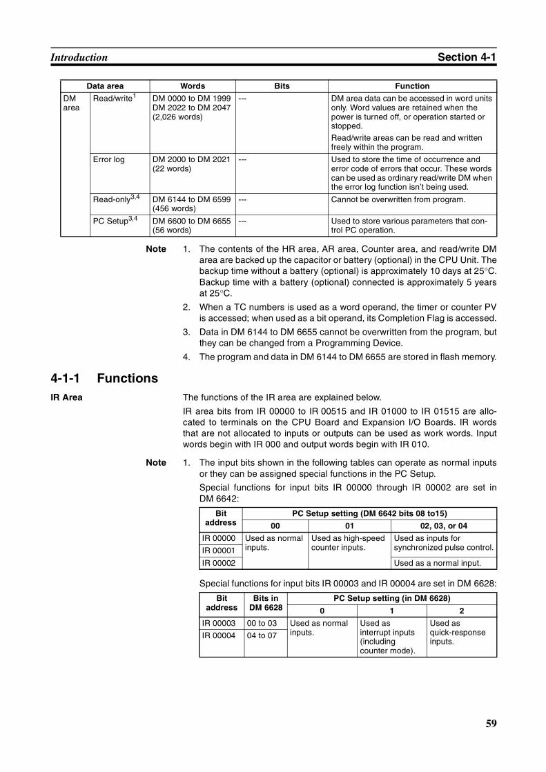
59
Introduction Section 4-1
Note 1. The contents of the HR area, AR area, Counter area, and read/write DMarea are backed up the capacitor or battery (optional) in the CPU Unit. Thebackup time without a battery (optional) is approximately 10 days at 25°C.Backup time with a battery (optional) connected is approximately 5 yearsat 25°C.
2. When a TC numbers is used as a word operand, the timer or counter PVis accessed; when used as a bit operand, its Completion Flag is accessed.
3. Data in DM 6144 to DM 6655 cannot be overwritten from the program, butthey can be changed from a Programming Device.
4. The program and data in DM 6144 to DM 6655 are stored in flash memory.
4-1-1 FunctionsIR Area The functions of the IR area are explained below.
IR area bits from IR 00000 to IR 00515 and IR 01000 to IR 01515 are allo-cated to terminals on the CPU Board and Expansion I/O Boards. IR wordsthat are not allocated to inputs or outputs can be used as work words. Inputwords begin with IR 000 and output words begin with IR 010.
Note 1. The input bits shown in the following tables can operate as normal inputsor they can be assigned special functions in the PC Setup.
Special functions for input bits IR 00000 through IR 00002 are set inDM 6642:
Special functions for input bits IR 00003 and IR 00004 are set in DM 6628:
DM area
Read/write1 DM 0000 to DM 1999DM 2022 to DM 2047(2,026 words)
--- DM area data can be accessed in word units only. Word values are retained when the power is turned off, or operation started or stopped.
Read/write areas can be read and written freely within the program.
Error log DM 2000 to DM 2021(22 words)
--- Used to store the time of occurrence and error code of errors that occur. These words can be used as ordinary read/write DM when the error log function isn’t being used.
Read-only3,4 DM 6144 to DM 6599(456 words)
--- Cannot be overwritten from program.
PC Setup3,4 DM 6600 to DM 6655(56 words)
--- Used to store various parameters that con-trol PC operation.
Data area Words Bits Function
Bit address
PC Setup setting (DM 6642 bits 08 to15)
00 01 02, 03, or 04
IR 00000 Used as normal inputs.
Used as high-speed counter inputs.
Used as inputs for synchronized pulse control.IR 00001
IR 00002 Used as a normal input.
Bit address
Bits in DM 6628
PC Setup setting (in DM 6628)
0 1 2
IR 00003 00 to 03 Used as normal inputs.
Used as interrupt inputs (including counter mode).
Used as quick-response inputs.
IR 00004 04 to 07
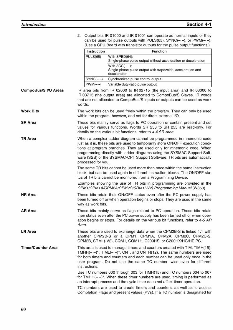
60
Introduction Section 4-1
2. Output bits IR 01000 and IR 01001 can operate as normal inputs or theycan be used for pulse outputs with PULS(65), SYNC(– –), or PWM(– –).(Use a CPU Board with transistor outputs for the pulse output functions.)
CompoBus/S I/O Areas IR area bits from IR 02000 to IR 02715 (the input area) and IR 03000 toIR 03715 (the output area) are allocated to CompoBus/S Slaves. IR wordsthat are not allocated to CompoBus/S inputs or outputs can be used as workwords.
Work Bits The work bits can be used freely within the program. They can only be usedwithin the program, however, and not for direct external I/O.
SR Area These bits mainly serve as flags to PC operation or contain present and setvalues for various functions. Words SR 253 to SR 255 are read-only. Fordetails on the various bit functions, refer to 4-4 SR Area.
TR Area When a complex ladder diagram cannot be programmed in mnemonic codejust as it is, these bits are used to temporarily store ON/OFF execution condi-tions at program branches. They are used only for mnemonic code. Whenprogramming directly with ladder diagrams using the SYSMAC Support Soft-ware (SSS) or the SYSMAC-CPT Support Software, TR bits are automaticallyprocessed for you.
The same TR bits cannot be used more than once within the same instructionblock, but can be used again in different instruction blocks. The ON/OFF sta-tus of TR bits cannot be monitored from a Programming Device.
Examples showing the use of TR bits in programming are provided in theCPM1/CPM1A/CPM2A/CPM2C/SRM1(-V2) Programming Manual (W353).
HR Area These bits retain their ON/OFF status even after the PC power supply hasbeen turned off or when operation begins or stops. They are used in the sameway as work bits.
AR Area These bits mainly serve as flags related to PC operation. These bits retaintheir status even after the PC power supply has been turned off or when oper-ation begins or stops. For details on the various bit functions, refer to 4-5 ARArea.
LR Area These bits are used to exchange data when the CPM2B-S is linked 1:1 withanother CPM2B-S or a CPM1, CPM1A, CPM2A, CPM2C, CPM2C-S,CPM2B, SRM1(-V2), CQM1, CQM1H, C200HS, or C200HX/HG/HE PC.
Timer/Counter Area This area is used to manage timers and counters created with TIM, TIMH(15),TMHH(– –)*, TIML(– –)*, CNT, and CNTR(12). The same numbers are usedfor both timers and counters and each number can be used only once in theuser program. Do not use the same TC number twice even for differentinstructions.
Use TC numbers 000 through 003 for TIMH(15) and TC numbers 004 to 007for TMHH(– –)*. When these timer numbers are used, timing is performed asan interrupt process and the cycle timer does not affect timer operation.
TC numbers are used to create timers and counters, as well as to accessCompletion Flags and present values (PVs). If a TC number is designated for
Instruction Function
PULS(65) With SPED(64):Single-phase pulse output without acceleration or deceleration
With ACC(– –):Single-phase pulse output with trapezoidal acceleration and deceleration
SYNC(– –) Synchronized pulse control output
PWM(– –) Variable duty-ratio pulse output

61
Introduction Section 4-1
word data, it will access the present value (PV); if it is used for bit data, it willaccess the Completion Flag for the timer/counter.
DM Area DM area data is accessed in word units only. The contents of the DM area areretained even after the PC power supply has been turned off or when opera-tion begins or stops.
DM words DM 0000 through DM 1999 and DM 2022 through DM 2047 can beused freely in the program; other DM words are allocated specific functions,described below.
DM 2000 through DM 2021 contain the error log information. Refer to Section9 Troubleshooting for details on the error log.
Note DM 6600 through DM 6655 contain the PC Setup. Refer to 4-6 PC Setup fordetails.
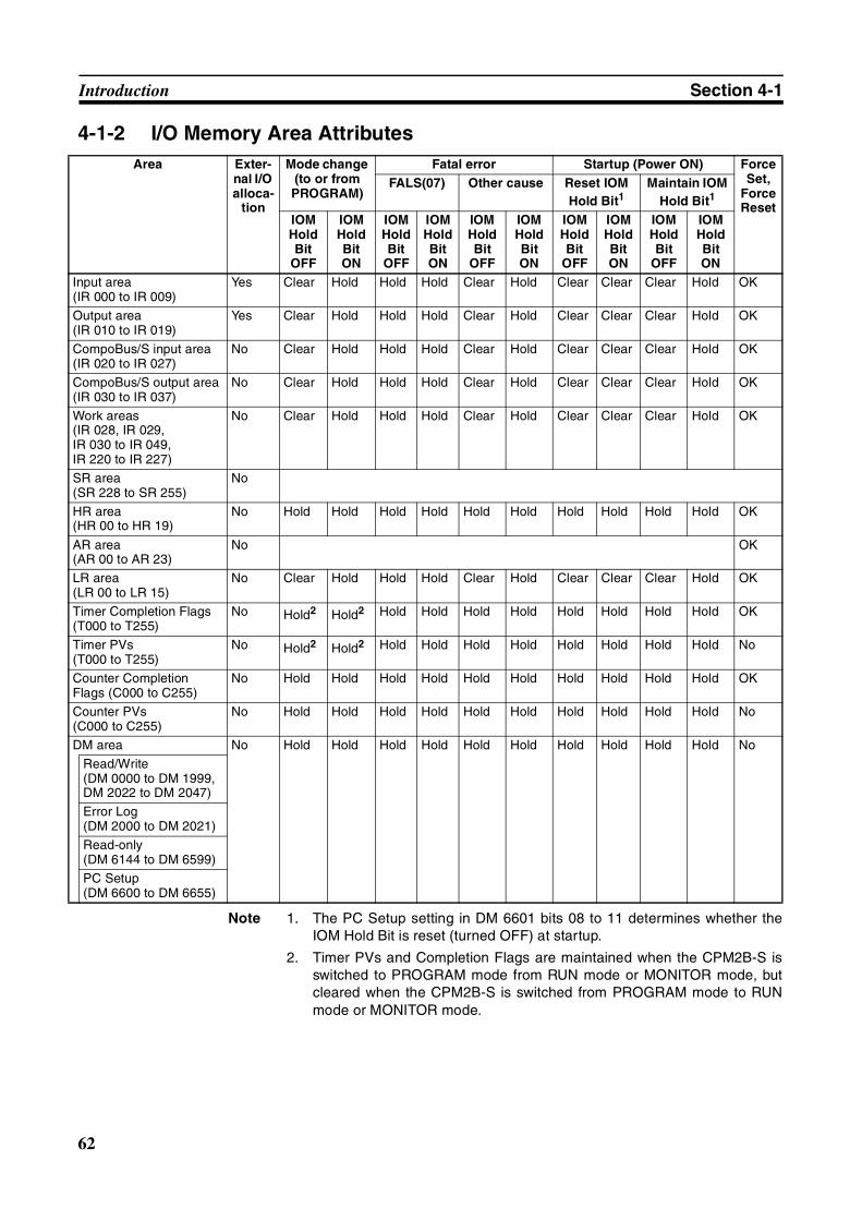
62
Introduction Section 4-1
4-1-2 I/O Memory Area Attributes
Note 1. The PC Setup setting in DM 6601 bits 08 to 11 determines whether theIOM Hold Bit is reset (turned OFF) at startup.
2. Timer PVs and Completion Flags are maintained when the CPM2B-S isswitched to PROGRAM mode from RUN mode or MONITOR mode, butcleared when the CPM2B-S is switched from PROGRAM mode to RUNmode or MONITOR mode.
Area Exter-nal I/O alloca-
tion
Mode change (to or from PROGRAM)
Fatal error Startup (Power ON) Force Set,
Force Reset
FALS(07) Other cause Reset IOM Hold Bit1
Maintain IOM Hold Bit1
IOM Hold Bit
OFF
IOM Hold Bit ON
IOM Hold Bit
OFF
IOM Hold Bit ON
IOM Hold Bit
OFF
IOM Hold Bit ON
IOM Hold Bit
OFF
IOM Hold Bit ON
IOM Hold Bit
OFF
IOM Hold Bit ON
Input area(IR 000 to IR 009)
Yes Clear Hold Hold Hold Clear Hold Clear Clear Clear Hold OK
Output area(IR 010 to IR 019)
Yes Clear Hold Hold Hold Clear Hold Clear Clear Clear Hold OK
CompoBus/S input area(IR 020 to IR 027)
No Clear Hold Hold Hold Clear Hold Clear Clear Clear Hold OK
CompoBus/S output area(IR 030 to IR 037)
No Clear Hold Hold Hold Clear Hold Clear Clear Clear Hold OK
Work areas(IR 028, IR 029,IR 030 to IR 049,IR 220 to IR 227)
No Clear Hold Hold Hold Clear Hold Clear Clear Clear Hold OK
SR area(SR 228 to SR 255)
No
HR area(HR 00 to HR 19)
No Hold Hold Hold Hold Hold Hold Hold Hold Hold Hold OK
AR area(AR 00 to AR 23)
No OK
LR area(LR 00 to LR 15)
No Clear Hold Hold Hold Clear Hold Clear Clear Clear Hold OK
Timer Completion Flags (T000 to T255)
No Hold2 Hold2 Hold Hold Hold Hold Hold Hold Hold Hold OK
Timer PVs(T000 to T255)
No Hold2 Hold2 Hold Hold Hold Hold Hold Hold Hold Hold No
Counter Completion Flags (C000 to C255)
No Hold Hold Hold Hold Hold Hold Hold Hold Hold Hold OK
Counter PVs(C000 to C255)
No Hold Hold Hold Hold Hold Hold Hold Hold Hold Hold No
DM area No Hold Hold Hold Hold Hold Hold Hold Hold Hold Hold No
Read/Write(DM 0000 to DM 1999, DM 2022 to DM 2047)
Error Log(DM 2000 to DM 2021)
Read-only(DM 6144 to DM 6599)
PC Setup(DM 6600 to DM 6655)
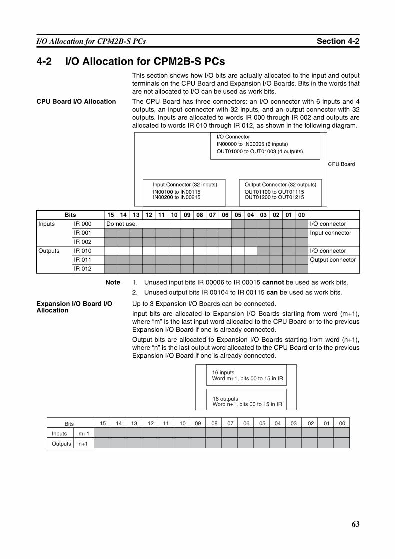
63
I/O Allocation for CPM2B-S PCs Section 4-2
4-2 I/O Allocation for CPM2B-S PCsThis section shows how I/O bits are actually allocated to the input and outputterminals on the CPU Board and Expansion I/O Boards. Bits in the words thatare not allocated to I/O can be used as work bits.
CPU Board I/O Allocation The CPU Board has three connectors: an I/O connector with 6 inputs and 4outputs, an input connector with 32 inputs, and an output connector with 32outputs. Inputs are allocated to words IR 000 through IR 002 and outputs areallocated to words IR 010 through IR 012, as shown in the following diagram.
Note 1. Unused input bits IR 00006 to IR 00015 cannot be used as work bits.
2. Unused output bits IR 00104 to IR 00115 can be used as work bits.
Expansion I/O Board I/O Allocation
Up to 3 Expansion I/O Boards can be connected.
Input bits are allocated to Expansion I/O Boards starting from word (m+1),where “m” is the last input word allocated to the CPU Board or to the previousExpansion I/O Board if one is already connected.
Output bits are allocated to Expansion I/O Boards starting from word (n+1),where “n” is the last output word allocated to the CPU Board or to the previousExpansion I/O Board if one is already connected.
I/O ConnectorIN00000 to IN00005 (6 inputs)OUT01000 to OUT01003 (4 outputs)
Output Connector (32 outputs)OUT01100 to OUT01115OUT01200 to OUT01215
Input Connector (32 inputs)IN00100 to IN00115IN00200 to IN00215
CPU Board
Bits 15 14 13 12 11 10 09 08 07 06 05 04 03 02 01 00
Inputs IR 000 Do not use. I/O connector
IR 001 Input connector
IR 002
Outputs IR 010 I/O connector
IR 011 Output connector
IR 012
16 inputsWord m+1, bits 00 to 15 in IR
16 outputsWord n+1, bits 00 to 15 in IR
Inputs
Outputs
m+1
n+1
15 14 13 12 11 10 09 08 07 06 05 04 03 02 01 00Bits
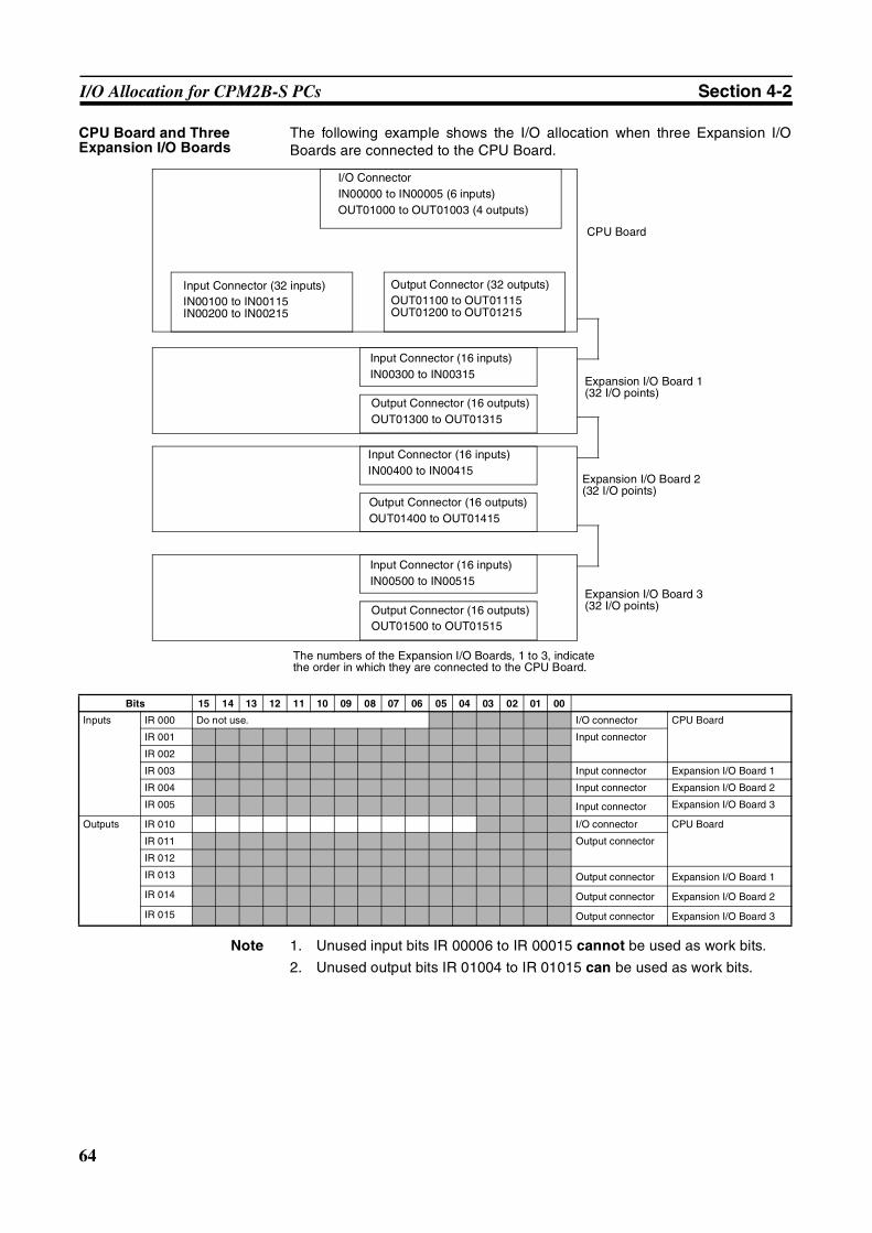
64
I/O Allocation for CPM2B-S PCs Section 4-2
CPU Board and Three Expansion I/O Boards
The following example shows the I/O allocation when three Expansion I/OBoards are connected to the CPU Board.
Note 1. Unused input bits IR 00006 to IR 00015 cannot be used as work bits.
2. Unused output bits IR 01004 to IR 01015 can be used as work bits.
Bits 15 14 13 12 11 10 09 08 07 06 05 04 03 02 01 00
Inputs IR 000 Do not use. I/O connector CPU Board
IR 001 Input connector
IR 002
IR 003 Input connector Expansion I/O Board 1
IR 004 Input connector Expansion I/O Board 2
IR 005 Input connector Expansion I/O Board 3
Outputs IR 010 I/O connector CPU Board
IR 011 Output connector
IR 012
IR 013 Output connector Expansion I/O Board 1
IR 014 Output connector Expansion I/O Board 2
IR 015 Output connector Expansion I/O Board 3
I/O ConnectorIN00000 to IN00005 (6 inputs)OUT01000 to OUT01003 (4 outputs)
Output Connector (32 outputs)OUT01100 to OUT01115OUT01200 to OUT01215
Input Connector (32 inputs)IN00100 to IN00115IN00200 to IN00215
CPU Board
Input Connector (16 inputs)IN00300 to IN00315
Output Connector (16 outputs)OUT01300 to OUT01315
Expansion I/O Board 1 (32 I/O points)
Input Connector (16 inputs)IN00400 to IN00415
Output Connector (16 outputs)OUT01400 to OUT01415
Input Connector (16 inputs)IN00500 to IN00515
Output Connector (16 outputs)OUT01500 to OUT01515
Expansion I/O Board 3 (32 I/O points)
Expansion I/O Board 2 (32 I/O points)
The numbers of the Expansion I/O Boards, 1 to 3, indicate the order in which they are connected to the CPU Board.
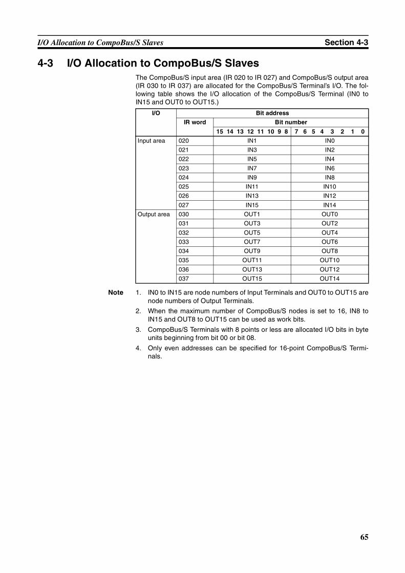
65
I/O Allocation to CompoBus/S Slaves Section 4-3
4-3 I/O Allocation to CompoBus/S SlavesThe CompoBus/S input area (IR 020 to IR 027) and CompoBus/S output area(IR 030 to IR 037) are allocated for the CompoBus/S Terminal’s I/O. The fol-lowing table shows the I/O allocation of the CompoBus/S Terminal (IN0 toIN15 and OUT0 to OUT15.)
Note 1. IN0 to IN15 are node numbers of Input Terminals and OUT0 to OUT15 arenode numbers of Output Terminals.
2. When the maximum number of CompoBus/S nodes is set to 16, IN8 toIN15 and OUT8 to OUT15 can be used as work bits.
3. CompoBus/S Terminals with 8 points or less are allocated I/O bits in byteunits beginning from bit 00 or bit 08.
4. Only even addresses can be specified for 16-point CompoBus/S Termi-nals.
I/O Bit address
IR word Bit number
15 14 13 12 11 10 9 8 7 6 5 4 3 2 1 0
Input area 020 IN1 IN0
021 IN3 IN2
022 IN5 IN4
023 IN7 IN6
024 IN9 IN8
025 IN11 IN10
026 IN13 IN12
027 IN15 IN14
Output area 030 OUT1 OUT0
031 OUT3 OUT2
032 OUT5 OUT4
033 OUT7 OUT6
034 OUT9 OUT8
035 OUT11 OUT10
036 OUT13 OUT12
037 OUT15 OUT14
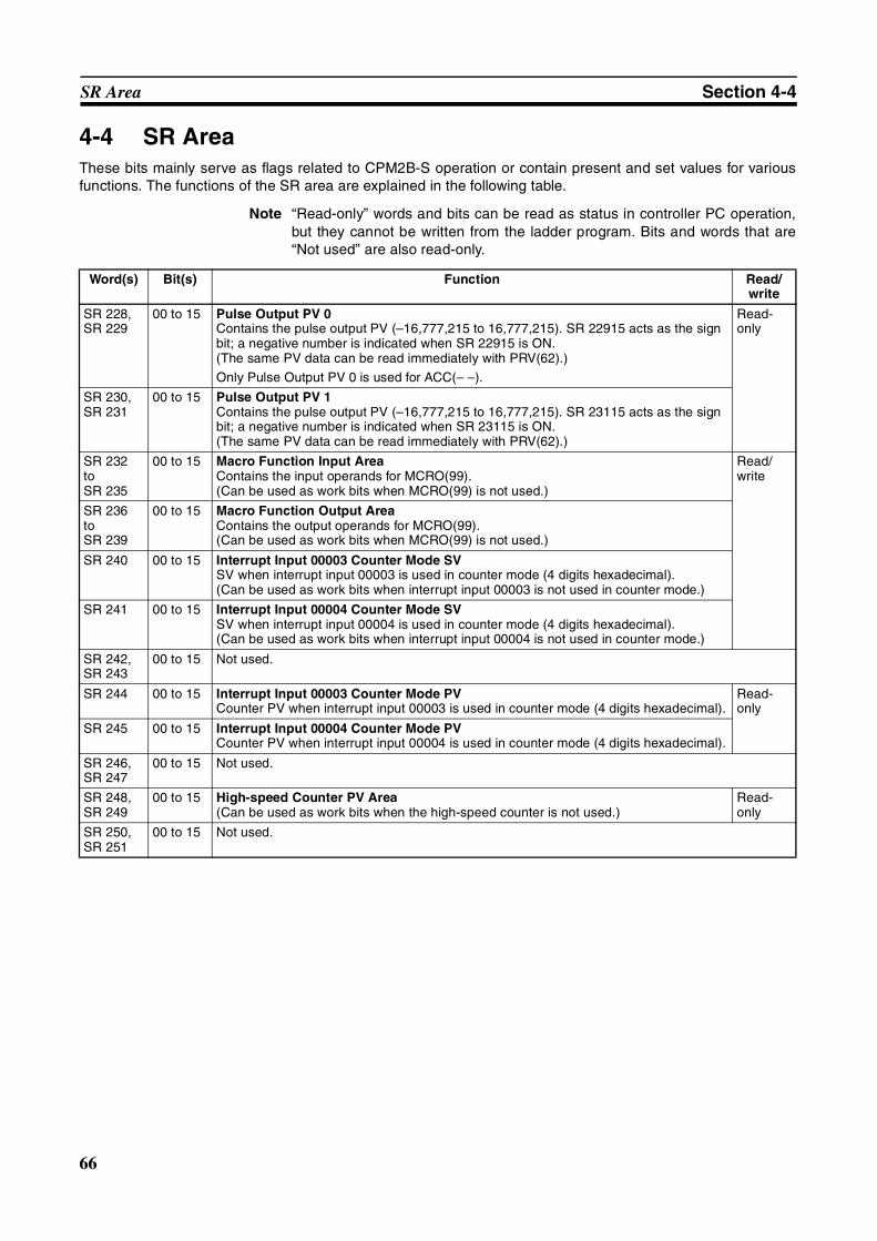
66
SR Area Section 4-4
4-4 SR AreaThese bits mainly serve as flags related to CPM2B-S operation or contain present and set values for variousfunctions. The functions of the SR area are explained in the following table.
Note “Read-only” words and bits can be read as status in controller PC operation,but they cannot be written from the ladder program. Bits and words that are“Not used” are also read-only.
Word(s) Bit(s) Function Read/ write
SR 228,SR 229
00 to 15 Pulse Output PV 0Contains the pulse output PV (–16,777,215 to 16,777,215). SR 22915 acts as the sign bit; a negative number is indicated when SR 22915 is ON.(The same PV data can be read immediately with PRV(62).)
Only Pulse Output PV 0 is used for ACC(– –).
Read-only
SR 230,SR 231
00 to 15 Pulse Output PV 1Contains the pulse output PV (–16,777,215 to 16,777,215). SR 23115 acts as the sign bit; a negative number is indicated when SR 23115 is ON.(The same PV data can be read immediately with PRV(62).)
SR 232toSR 235
00 to 15 Macro Function Input AreaContains the input operands for MCRO(99).(Can be used as work bits when MCRO(99) is not used.)
Read/ write
SR 236toSR 239
00 to 15 Macro Function Output AreaContains the output operands for MCRO(99).(Can be used as work bits when MCRO(99) is not used.)
SR 240 00 to 15 Interrupt Input 00003 Counter Mode SVSV when interrupt input 00003 is used in counter mode (4 digits hexadecimal).(Can be used as work bits when interrupt input 00003 is not used in counter mode.)
SR 241 00 to 15 Interrupt Input 00004 Counter Mode SVSV when interrupt input 00004 is used in counter mode (4 digits hexadecimal).(Can be used as work bits when interrupt input 00004 is not used in counter mode.)
SR 242, SR 243
00 to 15 Not used.
SR 244 00 to 15 Interrupt Input 00003 Counter Mode PVCounter PV when interrupt input 00003 is used in counter mode (4 digits hexadecimal).
Read-only
SR 245 00 to 15 Interrupt Input 00004 Counter Mode PVCounter PV when interrupt input 00004 is used in counter mode (4 digits hexadecimal).
SR 246, SR 247
00 to 15 Not used.
SR 248,SR 249
00 to 15 High-speed Counter PV Area(Can be used as work bits when the high-speed counter is not used.)
Read-only
SR 250, SR 251
00 to 15 Not used.
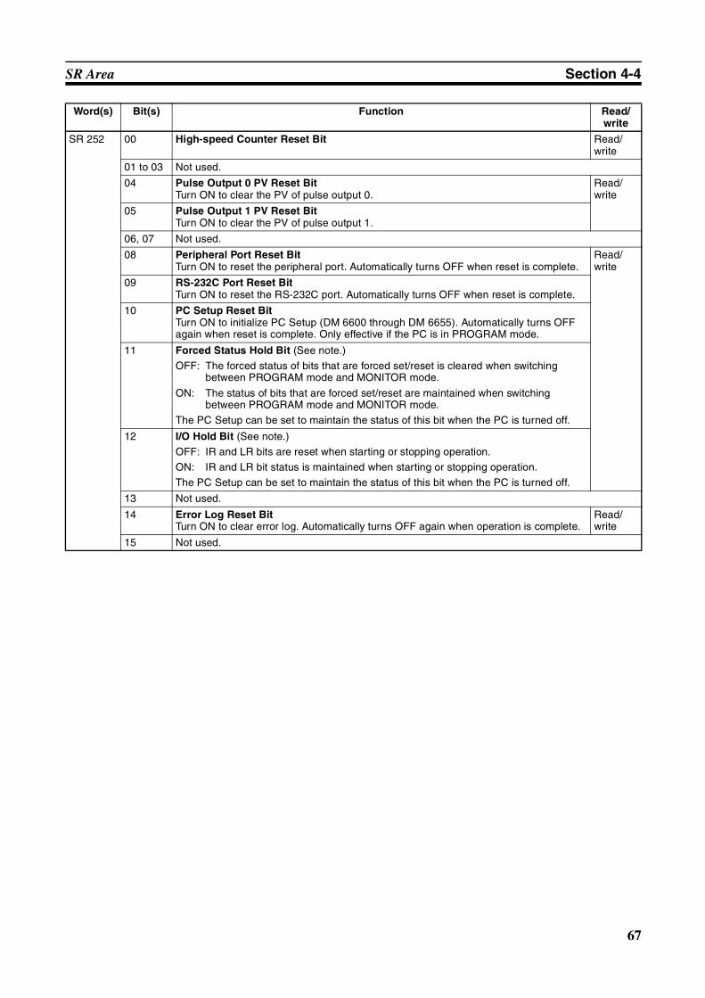
67
SR Area Section 4-4
SR 252 00 High-speed Counter Reset Bit Read/ write
01 to 03 Not used.
04 Pulse Output 0 PV Reset BitTurn ON to clear the PV of pulse output 0.
Read/ write
05 Pulse Output 1 PV Reset BitTurn ON to clear the PV of pulse output 1.
06, 07 Not used.
08 Peripheral Port Reset BitTurn ON to reset the peripheral port. Automatically turns OFF when reset is complete.
Read/ write
09 RS-232C Port Reset BitTurn ON to reset the RS-232C port. Automatically turns OFF when reset is complete.
10 PC Setup Reset BitTurn ON to initialize PC Setup (DM 6600 through DM 6655). Automatically turns OFF again when reset is complete. Only effective if the PC is in PROGRAM mode.
11 Forced Status Hold Bit (See note.)
OFF: The forced status of bits that are forced set/reset is cleared when switching between PROGRAM mode and MONITOR mode.
ON: The status of bits that are forced set/reset are maintained when switching between PROGRAM mode and MONITOR mode.
The PC Setup can be set to maintain the status of this bit when the PC is turned off.
12 I/O Hold Bit (See note.)
OFF: IR and LR bits are reset when starting or stopping operation.
ON: IR and LR bit status is maintained when starting or stopping operation.
The PC Setup can be set to maintain the status of this bit when the PC is turned off.
13 Not used.
14 Error Log Reset BitTurn ON to clear error log. Automatically turns OFF again when operation is complete.
Read/ write
15 Not used.
Word(s) Bit(s) Function Read/ write
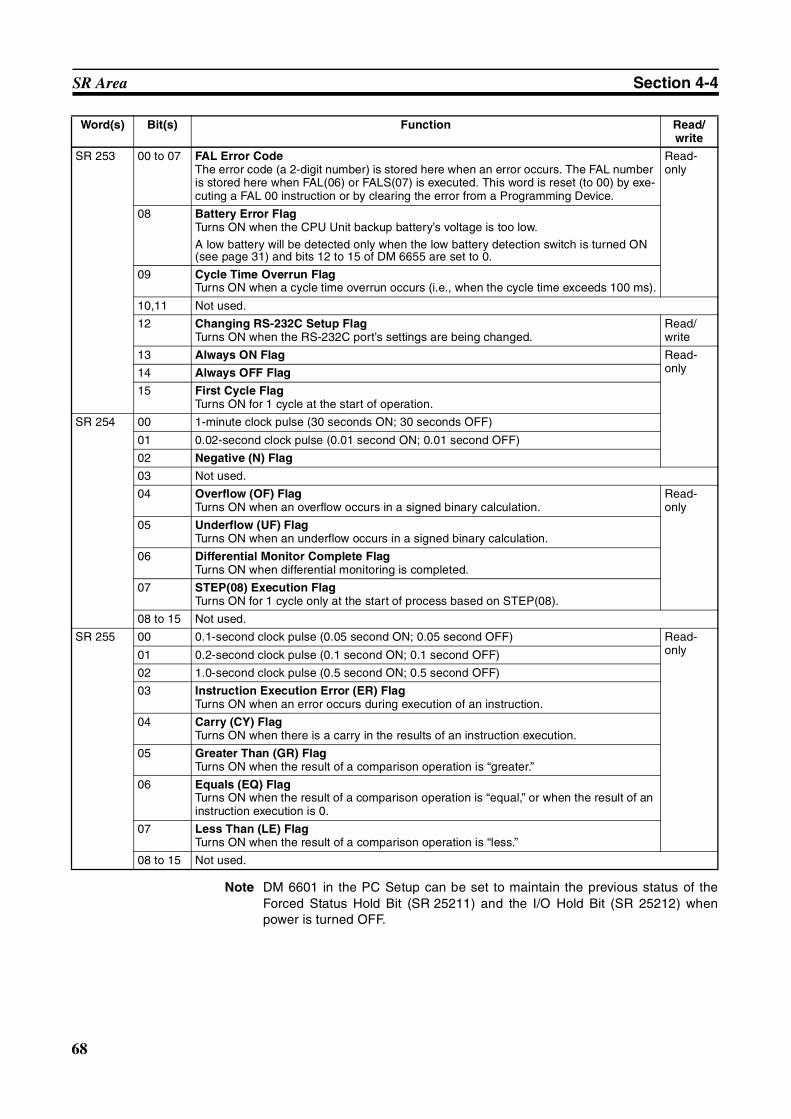
68
SR Area Section 4-4
Note DM 6601 in the PC Setup can be set to maintain the previous status of theForced Status Hold Bit (SR 25211) and the I/O Hold Bit (SR 25212) whenpower is turned OFF.
SR 253 00 to 07 FAL Error CodeThe error code (a 2-digit number) is stored here when an error occurs. The FAL number is stored here when FAL(06) or FALS(07) is executed. This word is reset (to 00) by exe-cuting a FAL 00 instruction or by clearing the error from a Programming Device.
Read-only
08 Battery Error FlagTurns ON when the CPU Unit backup battery’s voltage is too low.
A low battery will be detected only when the low battery detection switch is turned ON (see page 31) and bits 12 to 15 of DM 6655 are set to 0.
09 Cycle Time Overrun FlagTurns ON when a cycle time overrun occurs (i.e., when the cycle time exceeds 100 ms).
10,11 Not used.
12 Changing RS-232C Setup FlagTurns ON when the RS-232C port’s settings are being changed.
Read/ write
13 Always ON Flag Read-only14 Always OFF Flag
15 First Cycle FlagTurns ON for 1 cycle at the start of operation.
SR 254 00 1-minute clock pulse (30 seconds ON; 30 seconds OFF)
01 0.02-second clock pulse (0.01 second ON; 0.01 second OFF)
02 Negative (N) Flag
03 Not used.
04 Overflow (OF) FlagTurns ON when an overflow occurs in a signed binary calculation.
Read-only
05 Underflow (UF) FlagTurns ON when an underflow occurs in a signed binary calculation.
06 Differential Monitor Complete FlagTurns ON when differential monitoring is completed.
07 STEP(08) Execution FlagTurns ON for 1 cycle only at the start of process based on STEP(08).
08 to 15 Not used.
SR 255 00 0.1-second clock pulse (0.05 second ON; 0.05 second OFF) Read-only01 0.2-second clock pulse (0.1 second ON; 0.1 second OFF)
02 1.0-second clock pulse (0.5 second ON; 0.5 second OFF)
03 Instruction Execution Error (ER) FlagTurns ON when an error occurs during execution of an instruction.
04 Carry (CY) FlagTurns ON when there is a carry in the results of an instruction execution.
05 Greater Than (GR) FlagTurns ON when the result of a comparison operation is “greater.”
06 Equals (EQ) FlagTurns ON when the result of a comparison operation is “equal,” or when the result of an instruction execution is 0.
07 Less Than (LE) FlagTurns ON when the result of a comparison operation is “less.”
08 to 15 Not used.
Word(s) Bit(s) Function Read/ write
69
AR Area Section 4-5
4-5 AR AreaThese bits mainly serve as flags related to CPM2B-S operation such as error flags, high-speed counter flags,pulse output operation flags, and cycle time values. These bits retain their status even after the CPM2B-Spower supply has been turned off or when operation begins or stops.
Word(s) Bit(s) Function
AR 00
(-DRT only)
00 DeviceNet switch settings error (ON when a settings error occurred, OFF when normal.)
01 Node number duplication or Bus off error (ON when an error occurred, OFF when normal.)
02 DeviceNet network power supply error (ON when an error occurred, OFF when normal.)
03 DeviceNet communications error (ON when an error occurred, OFF when normal.)
04 to 06 Not used.
07 DeviceNet status error (ON when an error occurred, OFF when normal.)
08 Explicit Connection Flag ON: Connection established.OFF: Connection not established.09 Polling Connection Flag
10 Bit Strobe Connection Flag
11 to 14 Not used.
15 I/O Link in progress (ON when the I/O Link is operating, otherwise OFF.)
AR 01 00 to 15 Reserved for the system (These bits cannot be used.)
AR 02 00 Expansion Board Error Flag for 1st Unit These flags turn ON when there is an error in the corresponding Unit.01 Expansion Board Error Flag for 2nd Unit
02 Expansion Board Error Flag for 3rd Unit
03 to 07 Not used.
08 to 11 Number of Expansion I/O Boards connected
12 to 15 Not used.
AR 03 00 to 15 Not used.
AR 04 00 to 07 CompoBus/S Active Slave Flags for OUT 0 to OUT7 (ON when the Slave is communicating.)
08 to 15 CompoBus/S Slave Communications Error Flags for OUT 0 to OUT7
AR 05 00 to 07 CompoBus/S Active Slave Flags for IN0 to IN7 (ON when the Slave is communicating.)
08 to 15 CompoBus/S Slave Communications Error Flags for IN0 to IN7
AR 06 00 to 07 CompoBus/S Active Slave Flags for OUT 8 to OUT15 (ON when the Slave is communicating.)
08 to 15 CompoBus/S Slave Communications Error Flags for OUT 8 to OUT15
AR 07 00 to 07 CompoBus/S Active Slave Flags for IN8 to IN15 (ON when the Slave is communicating.)
08 to 15 CompoBus/S Slave Communications Error Flags for IN8 to IN15
70
AR Area Section 4-5
AR 08 00 to 03 RS-232C Port Error Code0: Normal completion1: Parity error2: Frame error3: Overrun error
04 RS-232C Communications Error FlagTurns ON when an RS-232C port communications error occurs.
05 RS-232C Transmit Ready FlagTurns ON when the PC is ready to transmit data. (No-protocol and Host Link only)
06 RS-232C Reception Completed FlagTurns ON when the PC has completed reading data. (No-protocol only)
07 RS-232C Reception Overflow FlagTurns ON when an overflow has occurred. (No-protocol only)
08 to 11 Peripheral Port Error Code0: Normal completion1: Parity error2: Frame error3: Overrun error
12 Peripheral Port Communications Error FlagTurns ON when a peripheral port communications error occurs.
13 Peripheral Port Transmit Ready FlagTurns ON when the PC is ready to transmit data. (No-protocol and Host Link only)
14 Peripheral Port Reception Completed FlagTurns ON when the PC has completed reading data. (No-protocol only)
15 Peripheral Port Reception Overflow FlagTurns ON when an overflow has occurred. (No-protocol only)
AR 09 00 to 15 RS-232C Port Reception Counter (4 digits BCD)Valid only when no-protocol communications are used.
AR 10 00 to 15 Peripheral Port Reception Counter (4 digits BCD)Valid only when no-protocol communications are used.
Word(s) Bit(s) Function
71
AR Area Section 4-5
AR 11
(Note 1)
00 to 07 High-speed Counter Range Comparison Flags00 ON: Counter PV is within comparison range 101 ON: Counter PV is within comparison range 202 ON: Counter PV is within comparison range 303 ON: Counter PV is within comparison range 404 ON: Counter PV is within comparison range 505 ON: Counter PV is within comparison range 606 ON: Counter PV is within comparison range 707 ON: Counter PV is within comparison range 8
08 High-speed Counter Comparison OperationON: OperatingOFF: Stopped
09 High-speed Counter PV Overflow/Underflow FlagON: An overflow or underflow occurred.OFF: Normal operation
10 Not used.
11 Pulse Output 0 Output StatusON: Pulse output 0 is accelerating or decelerating.OFF: Pulse output 0 is operating at a constant rate.
12 Pulse Output 0 Overflow/Underflow FlagON: An overflow or underflow occurred.OFF: Normal operation
13 Pulse Output 0 Pulse Quantity Set FlagON: Pulse quantity has been set.OFF: Pulse quantity has not been set.
14 Pulse Output 0 Pulse Output Completed FlagON: CompletedOFF: Not completed
15 Pulse Output 0 Output StatusON: Pulses being output.OFF: Stopped.
AR 12
(Note 1)
00 to 11 Not used.
12 Pulse Output 1 Overflow/Underflow FlagON: An overflow or underflow occurred.OFF: Normal operation
13 Pulse Output 1 Pulse Quantity Set FlagON: Pulse quantity has been set.OFF: Pulse quantity has not been set.
14 Pulse Output 1 Pulse Output Completed FlagON: CompletedOFF: Not completed
15 Pulse Output 1 Output StatusON: Pulses being output.OFF: Stopped.
Word(s) Bit(s) Function
72
AR Area Section 4-5
AR 13 00 Power-up PC Setup Error FlagTurns ON when there is an error in DM 6600 to DM 6614 (the part of the PC Setup area that is read at power-up).
01 Start-up PC Setup Error FlagTurns ON when there is an error in DM 6615 to DM 6644 (the part of the PC Setup area that is read at the beginning of operation).
02 RUN PC Setup Error FlagTurns ON when there is an error in DM 6645 to DM 6655 (the part of the PC Setup area that is always read).
03, 04 Not used.
05 Cycle Time Too Long FlagTurns ON if the actual cycle time is longer than the cycle time set in DM 6619.
06, 07 Not used.
08 Memory Area Specification Error FlagTurns ON when a non-existent data area address is specified in the program.
09 Flash Memory Error FlagTurns ON when there is an error in flash memory.
10 Read-only DM Error FlagTurns ON when a checksum error occurs in the read-only DM (DM 6144 to DM 6599) and that area is initialized.
11 PC Setup Error FlagTurns ON when a checksum error occurs in the PC Setup area.
12 Program Error FlagTurns ON when a checksum error occurs in the program memory (UM) area, or when an improper instruction is executed.
13 Expansion Instruction Area Error FlagTurns ON when a checksum error occurs in the expansion instruction assignments area. The expansion instruction assignments will be cleared to their default settings.
14 Data Save Error FlagTurns ON if data could not be retained with the backup battery.
The following words are normally backed up by the battery:DM read/write words (DM 0000 to DM 1999 and DM 2022 to DM 2047), Error Log (DM 2000 to DM 2021), HR area, counter area, SR 25511, SR 25512 (if DM 6601 is set to hold I/O memory at startup), AR 23, operating mode (if DM 6600 is set to use the previous operating mode), and clock words (AR 17 to AR 21, for CPU Units with clocks).
If the above words cannot be retained, all data will be cleared except that AR 2114 will be turned ON. The CPU Unit will start in PROGRAM mode if DM 6600 is set to use the previous operating mode. (If DM 6604 is set to generate an error, the PC will start in PROGRAM mode regardless.)
15 CompoBus/S ASIC Error FlagTurns ON if an error occurred.
AR 14 00 to 15 Maximum Cycle Time (4 digits BCD, see note 2)The longest cycle time since the beginning of operation is stored. It is not cleared when operation stops, but it is cleared when operation starts again.
AR 15 00 to 15 Current Cycle Time (4 digits BCD, see note 2)The most recent cycle time during operation is stored. The Current Cycle Time is not cleared when operation stops.
AR 16 00 to 15 Not used.
AR 17 00 to 15 Not used.
AR 18 00 to 15 Not used.
AR 19 00 to 15 Not used.
AR 20 00 to 15 Not used.
AR 21 00 to 15 Not used.
AR 22 00 to 15 Not used.
AR 23 00 to 15 Power-off Counter (4 digits BCD)This is the count of the number of times that the power has been turned off.To clear the count, write “0000” from a Programming Device.
Word(s) Bit(s) Function
73
PC Setup Section 4-6
Note 1. The same data can be read immediately with PRV(62).
2. The units for the maximum and current cycle times are determined by thesetting in bits 08 to 15 of DM 6618. A setting of 00 specifies 0.1-ms units,01 specifies 0.1-ms units, 02 specifies 1-ms units, and 03 specifies 10-msunits.
4-6 PC Setup4-6-1 Overview
The PC Setup (DM 6600 to DM 6655) contains various settings that controlPC operation. Changes to the PC Setup are saved when the CPM2B-S isturned OFF, program execution is started, or program execution is stopped.
Always perform one of the following operations after changing the PC Setup:
• Switch the CPM2B-S to MONITOR mode or RUN mode.
• Turn the CPM2B-S OFF and then ON again.
Changing PC Setup Settings
The PC Setup (DM 6600 to DM 6655) can be edited from a ProgrammingDevice. The settings in DM 6600 to DM 6644 can be changed only when thePC is in PROGRAM mode. The settings in DM 6645 to DM 6655 can bechanged when the PC is in PROGRAM mode or MONITOR mode, althoughthe PC’s cycle time will be quite long when the settings are changed in MONI-TOR mode.
CPU Unit Access of PC Setup Settings
The CPM2B-S CPU Unit reads parts of the PC Setup at different points of PCoperation. The CPU Unit timing is as follows:
DM 6600 to DM 6614: Read once when the PC is turned ON.DM 6615 to DM 6644: Read once at the start of program execution.DM 6645 to DM 6655: Read regularly while the PC is ON.
PC Setup Errors If there is an error in the PC Setup settings, a non-fatal error (error code 9B)will be generated when the CPU Unit accesses that part of the PC Setup. ThePC Setup Error Flags (AR 1300 to AR 1302) indicate the part of the PC Setupwhere the error is located. The default setting (usually 0000) is used insteadof the incorrect setting.
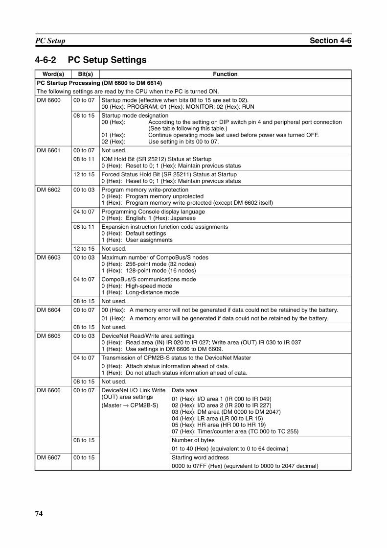
74
PC Setup Section 4-6
4-6-2 PC Setup SettingsWord(s) Bit(s) Function
PC Startup Processing (DM 6600 to DM 6614)The following settings are read by the CPU when the PC is turned ON.
DM 6600 00 to 07 Startup mode (effective when bits 08 to 15 are set to 02).00 (Hex): PROGRAM; 01 (Hex): MONITOR; 02 (Hex): RUN
08 to 15 Startup mode designation00 (Hex): According to the setting on DIP switch pin 4 and peripheral port connection
(See table following this table.)01 (Hex): Continue operating mode last used before power was turned OFF.02 (Hex): Use setting in bits 00 to 07.
DM 6601 00 to 07 Not used.
08 to 11 IOM Hold Bit (SR 25212) Status at Startup0 (Hex): Reset to 0; 1 (Hex): Maintain previous status
12 to 15 Forced Status Hold Bit (SR 25211) Status at Startup0 (Hex): Reset to 0; 1 (Hex): Maintain previous status
DM 6602 00 to 03 Program memory write-protection0 (Hex): Program memory unprotected1 (Hex): Program memory write-protected (except DM 6602 itself)
04 to 07 Programming Console display language0 (Hex): English; 1 (Hex): Japanese
08 to 11 Expansion instruction function code assignments0 (Hex): Default settings1 (Hex): User assignments
12 to 15 Not used.
DM 6603 00 to 03 Maximum number of CompoBus/S nodes0 (Hex): 256-point mode (32 nodes)1 (Hex): 128-point mode (16 nodes)
04 to 07 CompoBus/S communications mode0 (Hex): High-speed mode1 (Hex): Long-distance mode
08 to 15 Not used.
DM 6604 00 to 07 00 (Hex): A memory error will not be generated if data could not be retained by the battery.
01 (Hex): A memory error will be generated if data could not be retained by the battery.
08 to 15 Not used.
DM 6605 00 to 03 DeviceNet Read/Write area settings0 (Hex): Read area (IN) IR 020 to IR 027; Write area (OUT) IR 030 to IR 0371 (Hex): Use settings in DM 6606 to DM 6609.
04 to 07 Transmission of CPM2B-S status to the DeviceNet Master
0 (Hex): Attach status information ahead of data.1 (Hex): Do not attach status information ahead of data.
08 to 15 Not used.
DM 6606 00 to 07 DeviceNet I/O Link Write (OUT) area settings
(Master → CPM2B-S)
Data area
01 (Hex): I/O area 1 (IR 000 to IR 049)02 (Hex): I/O area 2 (IR 200 to IR 227)03 (Hex): DM area (DM 0000 to DM 2047)04 (Hex): LR area (LR 00 to LR 15)05 (Hex): HR area (HR 00 to HR 19)07 (Hex): Timer/counter area (TC 000 to TC 255)
08 to 15 Number of bytes
01 to 40 (Hex) (equivalent to 0 to 64 decimal)
DM 6607 00 to 15 Starting word address
0000 to 07FF (Hex) (equivalent to 0000 to 2047 decimal)
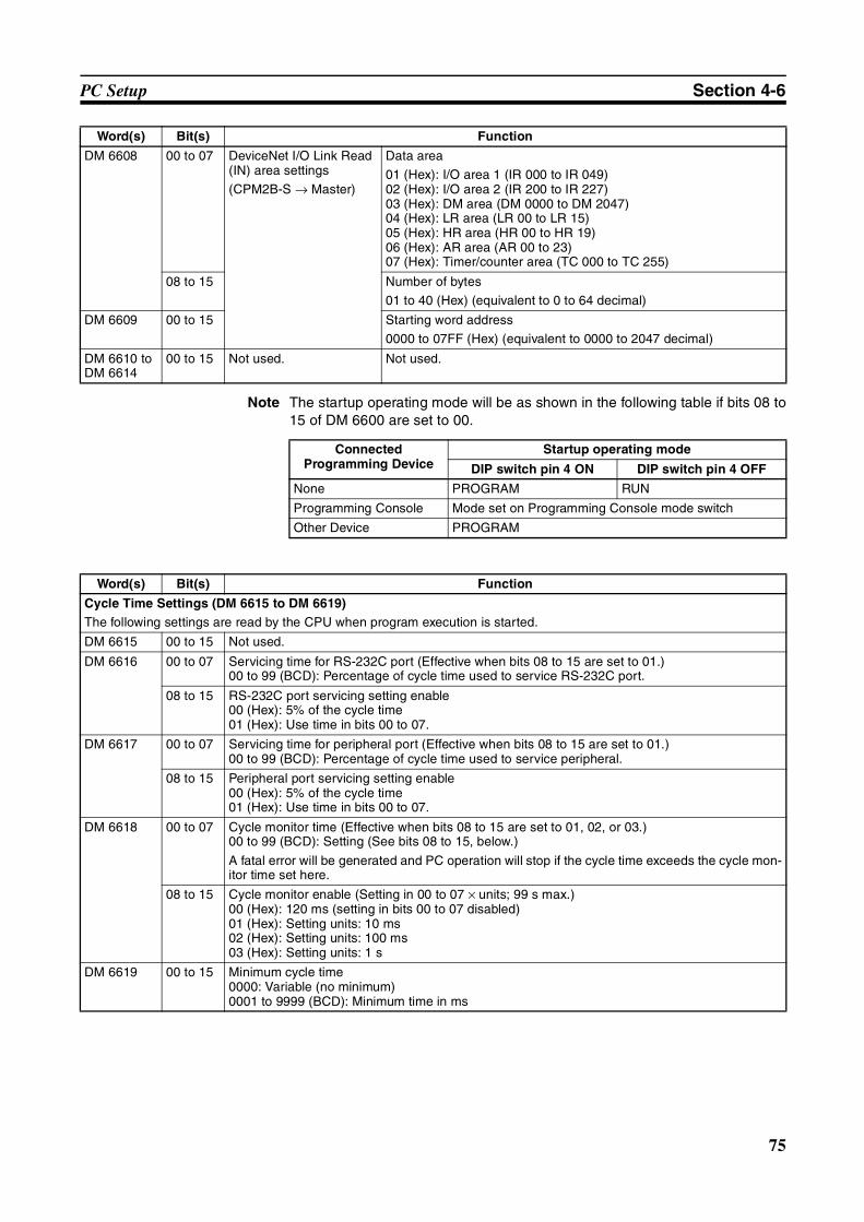
75
PC Setup Section 4-6
Note The startup operating mode will be as shown in the following table if bits 08 to15 of DM 6600 are set to 00.
DM 6608 00 to 07 DeviceNet I/O Link Read (IN) area settings
(CPM2B-S → Master)
Data area
01 (Hex): I/O area 1 (IR 000 to IR 049)02 (Hex): I/O area 2 (IR 200 to IR 227)03 (Hex): DM area (DM 0000 to DM 2047)04 (Hex): LR area (LR 00 to LR 15)05 (Hex): HR area (HR 00 to HR 19)06 (Hex): AR area (AR 00 to 23)07 (Hex): Timer/counter area (TC 000 to TC 255)
08 to 15 Number of bytes
01 to 40 (Hex) (equivalent to 0 to 64 decimal)
DM 6609 00 to 15 Starting word address
0000 to 07FF (Hex) (equivalent to 0000 to 2047 decimal)
DM 6610 to DM 6614
00 to 15 Not used. Not used.
Connected Programming Device
Startup operating mode
DIP switch pin 4 ON DIP switch pin 4 OFF
None PROGRAM RUN
Programming Console Mode set on Programming Console mode switch
Other Device PROGRAM
Word(s) Bit(s) Function
Word(s) Bit(s) Function
Cycle Time Settings (DM 6615 to DM 6619)The following settings are read by the CPU when program execution is started.
DM 6615 00 to 15 Not used.
DM 6616 00 to 07 Servicing time for RS-232C port (Effective when bits 08 to 15 are set to 01.)00 to 99 (BCD): Percentage of cycle time used to service RS-232C port.
08 to 15 RS-232C port servicing setting enable00 (Hex): 5% of the cycle time01 (Hex): Use time in bits 00 to 07.
DM 6617 00 to 07 Servicing time for peripheral port (Effective when bits 08 to 15 are set to 01.)00 to 99 (BCD): Percentage of cycle time used to service peripheral.
08 to 15 Peripheral port servicing setting enable00 (Hex): 5% of the cycle time01 (Hex): Use time in bits 00 to 07.
DM 6618 00 to 07 Cycle monitor time (Effective when bits 08 to 15 are set to 01, 02, or 03.)00 to 99 (BCD): Setting (See bits 08 to 15, below.)
A fatal error will be generated and PC operation will stop if the cycle time exceeds the cycle mon-itor time set here.
08 to 15 Cycle monitor enable (Setting in 00 to 07 × units; 99 s max.)00 (Hex): 120 ms (setting in bits 00 to 07 disabled)01 (Hex): Setting units: 10 ms02 (Hex): Setting units: 100 ms03 (Hex): Setting units: 1 s
DM 6619 00 to 15 Minimum cycle time0000: Variable (no minimum)0001 to 9999 (BCD): Minimum time in ms
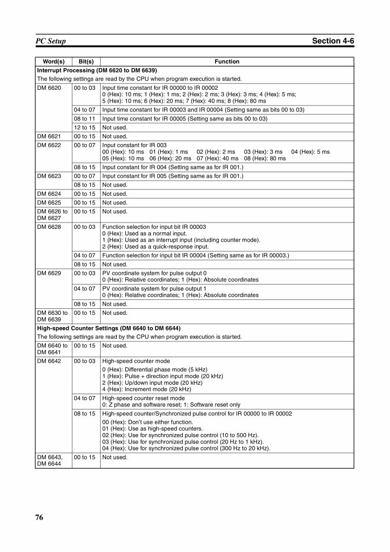
76
PC Setup Section 4-6
Interrupt Processing (DM 6620 to DM 6639)The following settings are read by the CPU when program execution is started.
DM 6620 00 to 03 Input time constant for IR 00000 to IR 000020 (Hex): 10 ms; 1 (Hex): 1 ms; 2 (Hex): 2 ms; 3 (Hex): 3 ms; 4 (Hex): 5 ms;5 (Hex): 10 ms; 6 (Hex): 20 ms; 7 (Hex): 40 ms; 8 (Hex): 80 ms
04 to 07 Input time constant for IR 00003 and IR 00004 (Setting same as bits 00 to 03)
08 to 11 Input time constant for IR 00005 (Setting same as bits 00 to 03)
12 to 15 Not used.
DM 6621 00 to 15 Not used.
DM 6622 00 to 07 Input constant for IR 00300 (Hex): 10 ms 01 (Hex): 1 ms 02 (Hex): 2 ms 03 (Hex): 3 ms 04 (Hex): 5 ms05 (Hex): 10 ms 06 (Hex): 20 ms 07 (Hex): 40 ms 08 (Hex): 80 ms
08 to 15 Input constant for IR 004 (Setting same as for IR 001.)
DM 6623 00 to 07 Input constant for IR 005 (Setting same as for IR 001.)
08 to 15 Not used.
DM 6624 00 to 15 Not used.
DM 6625 00 to 15 Not used.
DM 6626 to DM 6627
00 to 15 Not used.
DM 6628 00 to 03 Function selection for input bit IR 000030 (Hex): Used as a normal input.1 (Hex): Used as an interrupt input (including counter mode).2 (Hex): Used as a quick-response input.
04 to 07 Function selection for input bit IR 00004 (Setting same as for IR 00003.)
08 to 15 Not used.
DM 6629 00 to 03 PV coordinate system for pulse output 00 (Hex): Relative coordinates; 1 (Hex): Absolute coordinates
04 to 07 PV coordinate system for pulse output 10 (Hex): Relative coordinates; 1 (Hex): Absolute coordinates
08 to 15 Not used.
DM 6630 to DM 6639
00 to 15 Not used.
High-speed Counter Settings (DM 6640 to DM 6644)The following settings are read by the CPU when program execution is started.
DM 6640 to DM 6641
00 to 15 Not used.
DM 6642 00 to 03 High-speed counter mode
0 (Hex): Differential phase mode (5 kHz)1 (Hex): Pulse + direction input mode (20 kHz)2 (Hex): Up/down input mode (20 kHz)4 (Hex): Increment mode (20 kHz)
04 to 07 High-speed counter reset mode0: Z phase and software reset; 1: Software reset only
08 to 15 High-speed counter/Synchronized pulse control for IR 00000 to IR 00002
00 (Hex): Don’t use either function.01 (Hex): Use as high-speed counters.02 (Hex): Use for synchronized pulse control (10 to 500 Hz).03 (Hex): Use for synchronized pulse control (20 Hz to 1 kHz).04 (Hex): Use for synchronized pulse control (300 Hz to 20 kHz).
DM 6643, DM 6644
00 to 15 Not used.
Word(s) Bit(s) Function
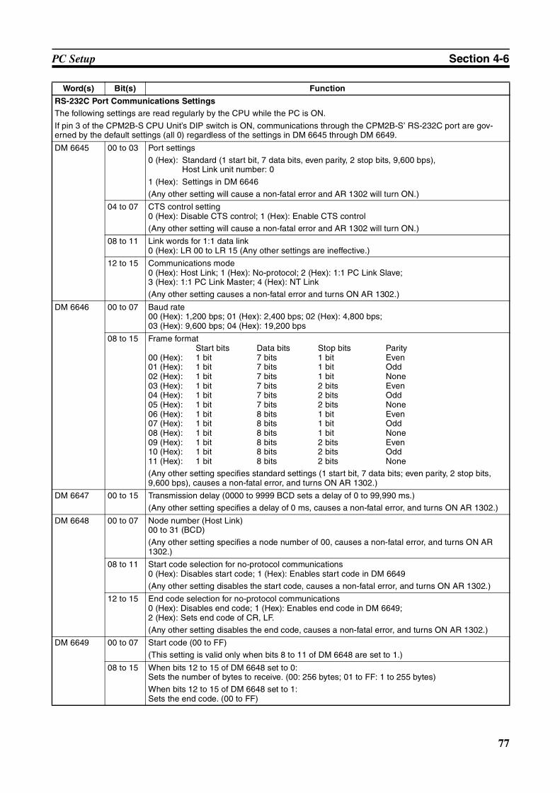
77
PC Setup Section 4-6
RS-232C Port Communications SettingsThe following settings are read regularly by the CPU while the PC is ON.
If pin 3 of the CPM2B-S CPU Unit’s DIP switch is ON, communications through the CPM2B-S’ RS-232C port are gov-erned by the default settings (all 0) regardless of the settings in DM 6645 through DM 6649.
DM 6645 00 to 03 Port settings
0 (Hex): Standard (1 start bit, 7 data bits, even parity, 2 stop bits, 9,600 bps),Host Link unit number: 0
1 (Hex): Settings in DM 6646
(Any other setting will cause a non-fatal error and AR 1302 will turn ON.)
04 to 07 CTS control setting0 (Hex): Disable CTS control; 1 (Hex): Enable CTS control
(Any other setting will cause a non-fatal error and AR 1302 will turn ON.)
08 to 11 Link words for 1:1 data link0 (Hex): LR 00 to LR 15 (Any other settings are ineffective.)
12 to 15 Communications mode0 (Hex): Host Link; 1 (Hex): No-protocol; 2 (Hex): 1:1 PC Link Slave;3 (Hex): 1:1 PC Link Master; 4 (Hex): NT Link
(Any other setting causes a non-fatal error and turns ON AR 1302.)
DM 6646 00 to 07 Baud rate00 (Hex): 1,200 bps; 01 (Hex): 2,400 bps; 02 (Hex): 4,800 bps;03 (Hex): 9,600 bps; 04 (Hex): 19,200 bps
08 to 15 Frame formatStart bits Data bits Stop bits Parity
00 (Hex): 1 bit 7 bits 1 bit Even01 (Hex): 1 bit 7 bits 1 bit Odd02 (Hex): 1 bit 7 bits 1 bit None03 (Hex): 1 bit 7 bits 2 bits Even04 (Hex): 1 bit 7 bits 2 bits Odd05 (Hex): 1 bit 7 bits 2 bits None06 (Hex): 1 bit 8 bits 1 bit Even07 (Hex): 1 bit 8 bits 1 bit Odd08 (Hex): 1 bit 8 bits 1 bit None09 (Hex): 1 bit 8 bits 2 bits Even10 (Hex): 1 bit 8 bits 2 bits Odd11 (Hex): 1 bit 8 bits 2 bits None
(Any other setting specifies standard settings (1 start bit, 7 data bits; even parity, 2 stop bits, 9,600 bps), causes a non-fatal error, and turns ON AR 1302.)
DM 6647 00 to 15 Transmission delay (0000 to 9999 BCD sets a delay of 0 to 99,990 ms.)
(Any other setting specifies a delay of 0 ms, causes a non-fatal error, and turns ON AR 1302.)
DM 6648 00 to 07 Node number (Host Link)00 to 31 (BCD)
(Any other setting specifies a node number of 00, causes a non-fatal error, and turns ON AR 1302.)
08 to 11 Start code selection for no-protocol communications0 (Hex): Disables start code; 1 (Hex): Enables start code in DM 6649
(Any other setting disables the start code, causes a non-fatal error, and turns ON AR 1302.)
12 to 15 End code selection for no-protocol communications0 (Hex): Disables end code; 1 (Hex): Enables end code in DM 6649;2 (Hex): Sets end code of CR, LF.
(Any other setting disables the end code, causes a non-fatal error, and turns ON AR 1302.)
DM 6649 00 to 07 Start code (00 to FF)
(This setting is valid only when bits 8 to 11 of DM 6648 are set to 1.)
08 to 15 When bits 12 to 15 of DM 6648 set to 0:Sets the number of bytes to receive. (00: 256 bytes; 01 to FF: 1 to 255 bytes)
When bits 12 to 15 of DM 6648 set to 1:Sets the end code. (00 to FF)
Word(s) Bit(s) Function
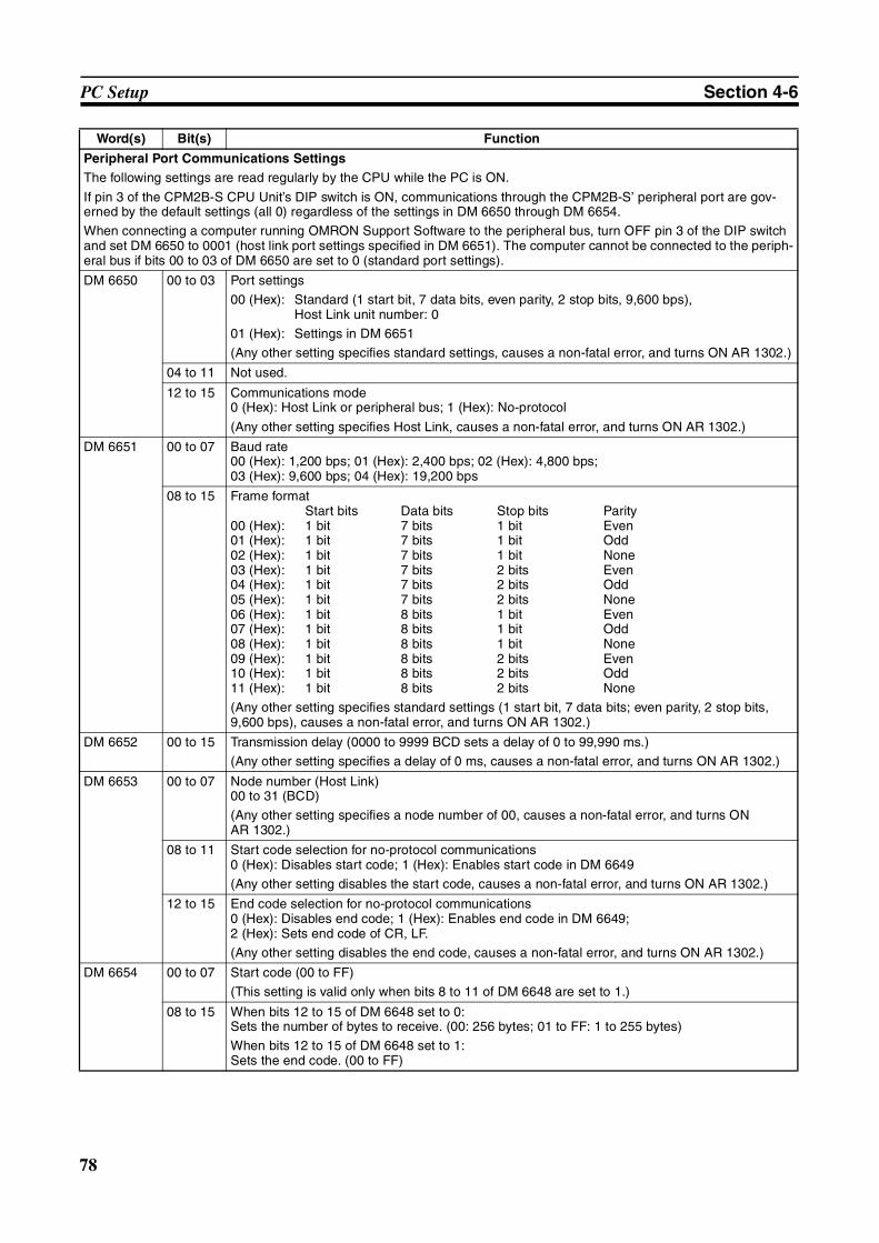
78
PC Setup Section 4-6
Peripheral Port Communications SettingsThe following settings are read regularly by the CPU while the PC is ON.
If pin 3 of the CPM2B-S CPU Unit’s DIP switch is ON, communications through the CPM2B-S’ peripheral port are gov-erned by the default settings (all 0) regardless of the settings in DM 6650 through DM 6654.
When connecting a computer running OMRON Support Software to the peripheral bus, turn OFF pin 3 of the DIP switch and set DM 6650 to 0001 (host link port settings specified in DM 6651). The computer cannot be connected to the periph-eral bus if bits 00 to 03 of DM 6650 are set to 0 (standard port settings).
DM 6650 00 to 03 Port settings
00 (Hex): Standard (1 start bit, 7 data bits, even parity, 2 stop bits, 9,600 bps),Host Link unit number: 0
01 (Hex): Settings in DM 6651
(Any other setting specifies standard settings, causes a non-fatal error, and turns ON AR 1302.)
04 to 11 Not used.
12 to 15 Communications mode0 (Hex): Host Link or peripheral bus; 1 (Hex): No-protocol
(Any other setting specifies Host Link, causes a non-fatal error, and turns ON AR 1302.)
DM 6651 00 to 07 Baud rate00 (Hex): 1,200 bps; 01 (Hex): 2,400 bps; 02 (Hex): 4,800 bps;03 (Hex): 9,600 bps; 04 (Hex): 19,200 bps
08 to 15 Frame formatStart bits Data bits Stop bits Parity
00 (Hex): 1 bit 7 bits 1 bit Even01 (Hex): 1 bit 7 bits 1 bit Odd02 (Hex): 1 bit 7 bits 1 bit None03 (Hex): 1 bit 7 bits 2 bits Even04 (Hex): 1 bit 7 bits 2 bits Odd05 (Hex): 1 bit 7 bits 2 bits None06 (Hex): 1 bit 8 bits 1 bit Even07 (Hex): 1 bit 8 bits 1 bit Odd08 (Hex): 1 bit 8 bits 1 bit None09 (Hex): 1 bit 8 bits 2 bits Even10 (Hex): 1 bit 8 bits 2 bits Odd11 (Hex): 1 bit 8 bits 2 bits None
(Any other setting specifies standard settings (1 start bit, 7 data bits; even parity, 2 stop bits, 9,600 bps), causes a non-fatal error, and turns ON AR 1302.)
DM 6652 00 to 15 Transmission delay (0000 to 9999 BCD sets a delay of 0 to 99,990 ms.)
(Any other setting specifies a delay of 0 ms, causes a non-fatal error, and turns ON AR 1302.)
DM 6653 00 to 07 Node number (Host Link)00 to 31 (BCD)
(Any other setting specifies a node number of 00, causes a non-fatal error, and turns ON AR 1302.)
08 to 11 Start code selection for no-protocol communications0 (Hex): Disables start code; 1 (Hex): Enables start code in DM 6649
(Any other setting disables the start code, causes a non-fatal error, and turns ON AR 1302.)
12 to 15 End code selection for no-protocol communications0 (Hex): Disables end code; 1 (Hex): Enables end code in DM 6649;2 (Hex): Sets end code of CR, LF.
(Any other setting disables the end code, causes a non-fatal error, and turns ON AR 1302.)
DM 6654 00 to 07 Start code (00 to FF)
(This setting is valid only when bits 8 to 11 of DM 6648 are set to 1.)
08 to 15 When bits 12 to 15 of DM 6648 set to 0:Sets the number of bytes to receive. (00: 256 bytes; 01 to FF: 1 to 255 bytes)
When bits 12 to 15 of DM 6648 set to 1:Sets the end code. (00 to FF)
Word(s) Bit(s) Function
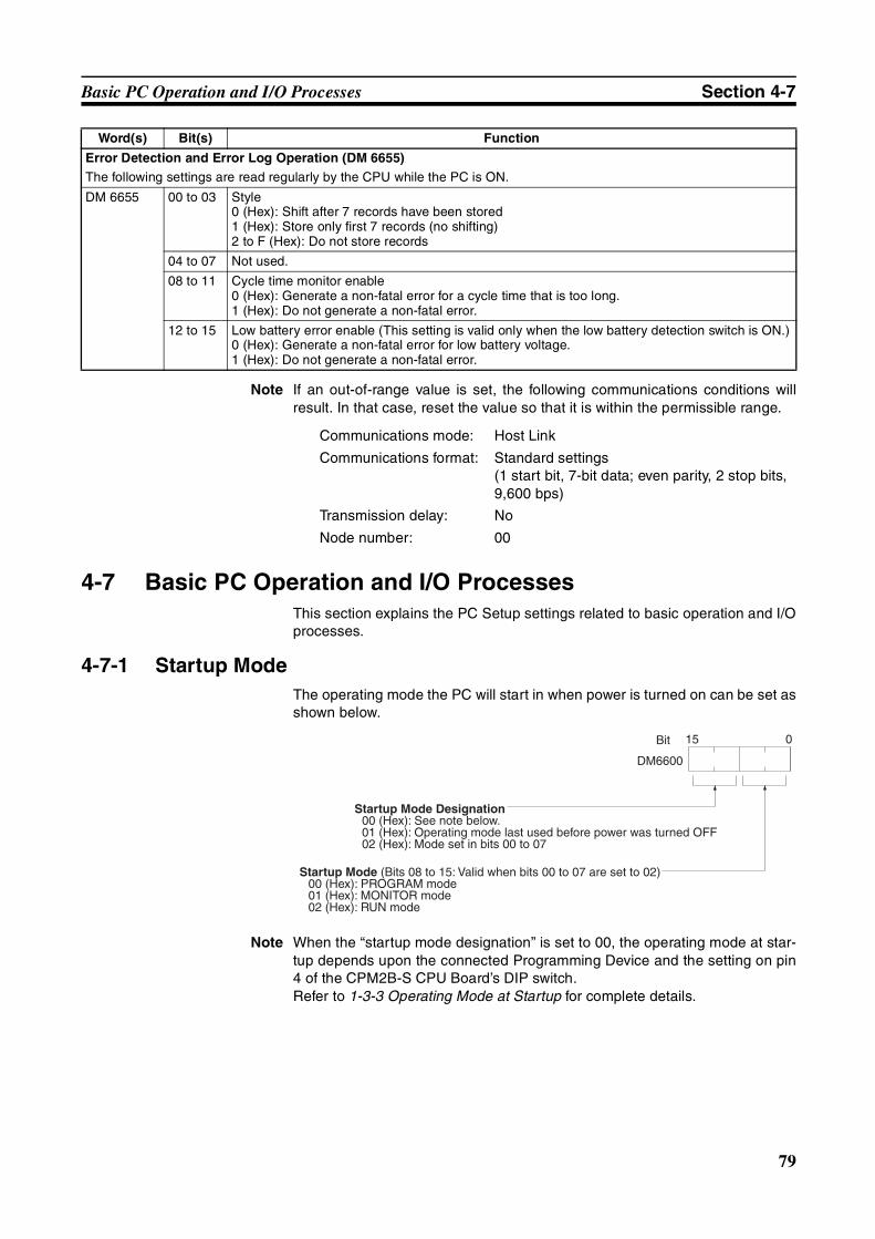
79
Basic PC Operation and I/O Processes Section 4-7
Note If an out-of-range value is set, the following communications conditions willresult. In that case, reset the value so that it is within the permissible range.
Communications mode: Host Link
Communications format: Standard settings (1 start bit, 7-bit data; even parity, 2 stop bits, 9,600 bps)
Transmission delay: No
Node number: 00
4-7 Basic PC Operation and I/O ProcessesThis section explains the PC Setup settings related to basic operation and I/Oprocesses.
4-7-1 Startup ModeThe operating mode the PC will start in when power is turned on can be set asshown below.
Note When the “startup mode designation” is set to 00, the operating mode at star-tup depends upon the connected Programming Device and the setting on pin4 of the CPM2B-S CPU Board’s DIP switch.Refer to 1-3-3 Operating Mode at Startup for complete details.
Error Detection and Error Log Operation (DM 6655)The following settings are read regularly by the CPU while the PC is ON.
DM 6655 00 to 03 Style0 (Hex): Shift after 7 records have been stored1 (Hex): Store only first 7 records (no shifting)2 to F (Hex): Do not store records
04 to 07 Not used.
08 to 11 Cycle time monitor enable0 (Hex): Generate a non-fatal error for a cycle time that is too long.1 (Hex): Do not generate a non-fatal error.
12 to 15 Low battery error enable (This setting is valid only when the low battery detection switch is ON.)0 (Hex): Generate a non-fatal error for low battery voltage.1 (Hex): Do not generate a non-fatal error.
Word(s) Bit(s) Function
15Bit
DM6600
0
Startup Mode Designation00 (Hex): See note below.01 (Hex): Operating mode last used before power was turned OFF02 (Hex): Mode set in bits 00 to 07
Startup Mode (Bits 08 to 15: Valid when bits 00 to 07 are set to 02)00 (Hex): PROGRAM mode01 (Hex): MONITOR mode02 (Hex): RUN mode
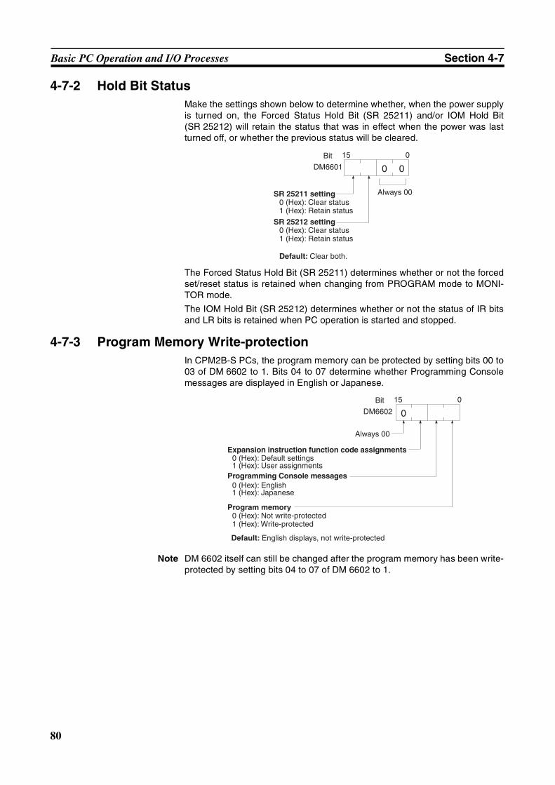
80
Basic PC Operation and I/O Processes Section 4-7
4-7-2 Hold Bit StatusMake the settings shown below to determine whether, when the power supplyis turned on, the Forced Status Hold Bit (SR 25211) and/or IOM Hold Bit(SR 25212) will retain the status that was in effect when the power was lastturned off, or whether the previous status will be cleared.
The Forced Status Hold Bit (SR 25211) determines whether or not the forcedset/reset status is retained when changing from PROGRAM mode to MONI-TOR mode.
The IOM Hold Bit (SR 25212) determines whether or not the status of IR bitsand LR bits is retained when PC operation is started and stopped.
4-7-3 Program Memory Write-protectionIn CPM2B-S PCs, the program memory can be protected by setting bits 00 to03 of DM 6602 to 1. Bits 04 to 07 determine whether Programming Consolemessages are displayed in English or Japanese.
Note DM 6602 itself can still be changed after the program memory has been write-protected by setting bits 04 to 07 of DM 6602 to 1.
15 0
0 0Bit
DM6601
SR 25211 setting0 (Hex): Clear status1 (Hex): Retain status
Always 00
SR 25212 setting0 (Hex): Clear status1 (Hex): Retain status
Default: Clear both.
15 0
0Bit
DM6602
Programming Console messages0 (Hex): English1 (Hex): Japanese
Program memory0 (Hex): Not write-protected1 (Hex): Write-protected
Default: English displays, not write-protected
Always 00
Expansion instruction function code assignments0 (Hex): Default settings1 (Hex): User assignments
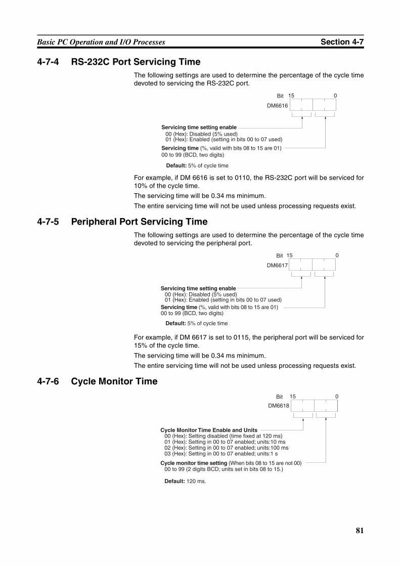
81
Basic PC Operation and I/O Processes Section 4-7
4-7-4 RS-232C Port Servicing TimeThe following settings are used to determine the percentage of the cycle timedevoted to servicing the RS-232C port.
For example, if DM 6616 is set to 0110, the RS-232C port will be serviced for10% of the cycle time.
The servicing time will be 0.34 ms minimum.
The entire servicing time will not be used unless processing requests exist.
4-7-5 Peripheral Port Servicing TimeThe following settings are used to determine the percentage of the cycle timedevoted to servicing the peripheral port.
For example, if DM 6617 is set to 0115, the peripheral port will be serviced for15% of the cycle time.
The servicing time will be 0.34 ms minimum.
The entire servicing time will not be used unless processing requests exist.
4-7-6 Cycle Monitor Time
15 0
Bit
Servicing time setting enable00 (Hex): Disabled (5% used)01 (Hex): Enabled (setting in bits 00 to 07 used)
Servicing time (%, valid with bits 08 to 15 are 01)00 to 99 (BCD, two digits)
Default: 5% of cycle time
DM6616
15 0
Bit
Servicing time setting enable00 (Hex): Disabled (5% used)01 (Hex): Enabled (setting in bits 00 to 07 used)
Servicing time (%, valid with bits 08 to 15 are 01)00 to 99 (BCD, two digits)
Default: 5% of cycle time
DM6617
15 0
DM6618 Bit
Cycle Monitor Time Enable and Units00 (Hex): Setting disabled (time fixed at 120 ms)01 (Hex): Setting in 00 to 07 enabled; units:10 ms02 (Hex): Setting in 00 to 07 enabled; units:100 ms03 (Hex): Setting in 00 to 07 enabled; units:1 s
Cycle monitor time setting (When bits 08 to 15 are not 00)00 to 99 (2 digits BCD; units set in bits 08 to 15.)
Default: 120 ms.
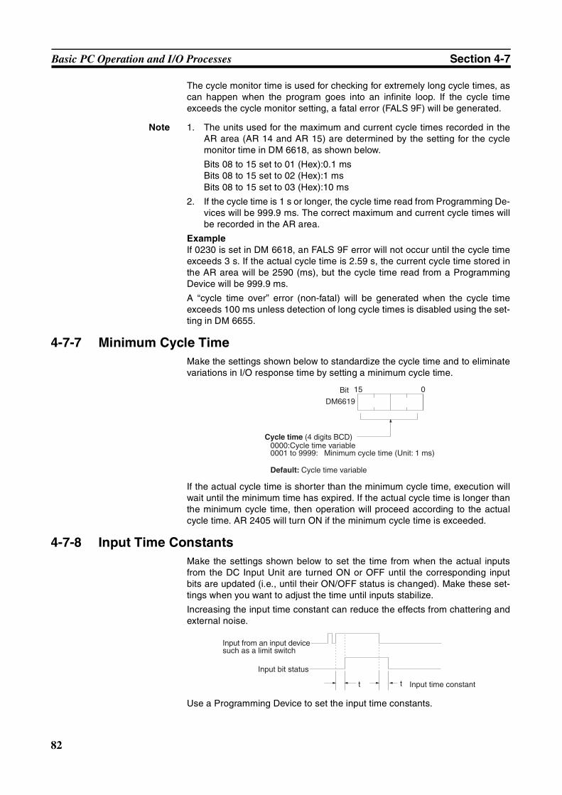
82
Basic PC Operation and I/O Processes Section 4-7
The cycle monitor time is used for checking for extremely long cycle times, ascan happen when the program goes into an infinite loop. If the cycle timeexceeds the cycle monitor setting, a fatal error (FALS 9F) will be generated.
Note 1. The units used for the maximum and current cycle times recorded in theAR area (AR 14 and AR 15) are determined by the setting for the cyclemonitor time in DM 6618, as shown below.
Bits 08 to 15 set to 01 (Hex):0.1 msBits 08 to 15 set to 02 (Hex):1 msBits 08 to 15 set to 03 (Hex):10 ms
2. If the cycle time is 1 s or longer, the cycle time read from Programming De-vices will be 999.9 ms. The correct maximum and current cycle times willbe recorded in the AR area.
ExampleIf 0230 is set in DM 6618, an FALS 9F error will not occur until the cycle timeexceeds 3 s. If the actual cycle time is 2.59 s, the current cycle time stored inthe AR area will be 2590 (ms), but the cycle time read from a ProgrammingDevice will be 999.9 ms.
A “cycle time over” error (non-fatal) will be generated when the cycle timeexceeds 100 ms unless detection of long cycle times is disabled using the set-ting in DM 6655.
4-7-7 Minimum Cycle TimeMake the settings shown below to standardize the cycle time and to eliminatevariations in I/O response time by setting a minimum cycle time.
If the actual cycle time is shorter than the minimum cycle time, execution willwait until the minimum time has expired. If the actual cycle time is longer thanthe minimum cycle time, then operation will proceed according to the actualcycle time. AR 2405 will turn ON if the minimum cycle time is exceeded.
4-7-8 Input Time ConstantsMake the settings shown below to set the time from when the actual inputsfrom the DC Input Unit are turned ON or OFF until the corresponding inputbits are updated (i.e., until their ON/OFF status is changed). Make these set-tings when you want to adjust the time until inputs stabilize.
Increasing the input time constant can reduce the effects from chattering andexternal noise.
Use a Programming Device to set the input time constants.
15 0Bit
DM6619
Cycle time (4 digits BCD)0000:Cycle time variable0001 to 9999: Minimum cycle time (Unit: 1 ms)
Default: Cycle time variable
Input from an input device such as a limit switch
Input bit status
Input time constantt t
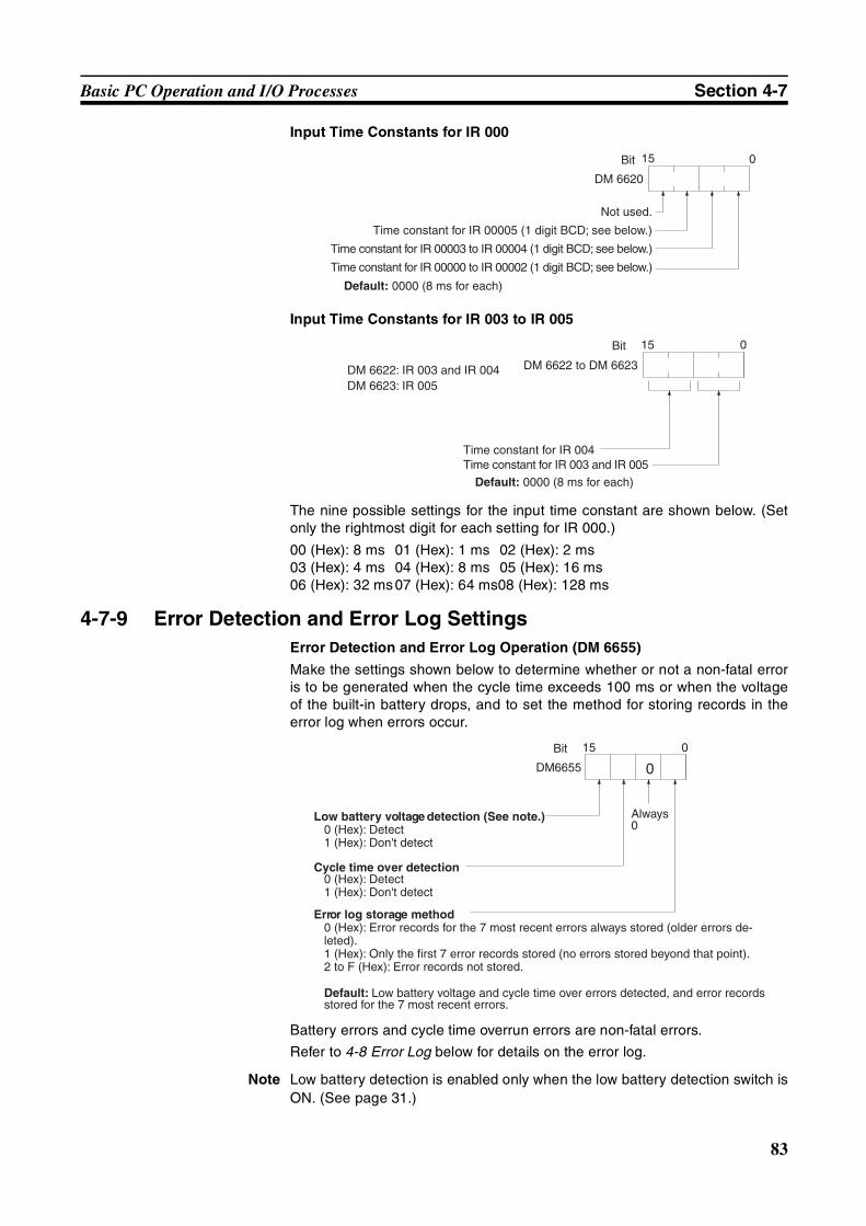
83
Basic PC Operation and I/O Processes Section 4-7
Input Time Constants for IR 000
Input Time Constants for IR 003 to IR 005
The nine possible settings for the input time constant are shown below. (Setonly the rightmost digit for each setting for IR 000.)
00 (Hex): 8 ms 01 (Hex): 1 ms 02 (Hex): 2 ms03 (Hex): 4 ms 04 (Hex): 8 ms 05 (Hex): 16 ms06 (Hex): 32 ms07 (Hex): 64 ms08 (Hex): 128 ms
4-7-9 Error Detection and Error Log SettingsError Detection and Error Log Operation (DM 6655)
Make the settings shown below to determine whether or not a non-fatal erroris to be generated when the cycle time exceeds 100 ms or when the voltageof the built-in battery drops, and to set the method for storing records in theerror log when errors occur.
Battery errors and cycle time overrun errors are non-fatal errors.
Refer to 4-8 Error Log below for details on the error log.
Note Low battery detection is enabled only when the low battery detection switch isON. (See page 31.)
15 0Bit
Not used.
Time constant for IR 00005 (1 digit BCD; see below.)
Time constant for IR 00003 to IR 00004 (1 digit BCD; see below.)
Time constant for IR 00000 to IR 00002 (1 digit BCD; see below.)
Default: 0000 (8 ms for each)
DM 6620
15 0
Bit
DM 6622: IR 003 and IR 004DM 6623: IR 005
Time constant for IR 004Time constant for IR 003 and IR 005
Default: 0000 (8 ms for each)
DM 6622 to DM 6623
Low battery voltage detection (See note.)0 (Hex): Detect1 (Hex): Don't detect
15 0
DM6655 0 Bit
Always 0
Cycle time over detection0 (Hex): Detect1 (Hex): Don't detect
Error log storage method0 (Hex): Error records for the 7 most recent errors always stored (older errors de-leted).1 (Hex): Only the first 7 error records stored (no errors stored beyond that point).2 to F (Hex): Error records not stored.
Default: Low battery voltage and cycle time over errors detected, and error records stored for the 7 most recent errors.
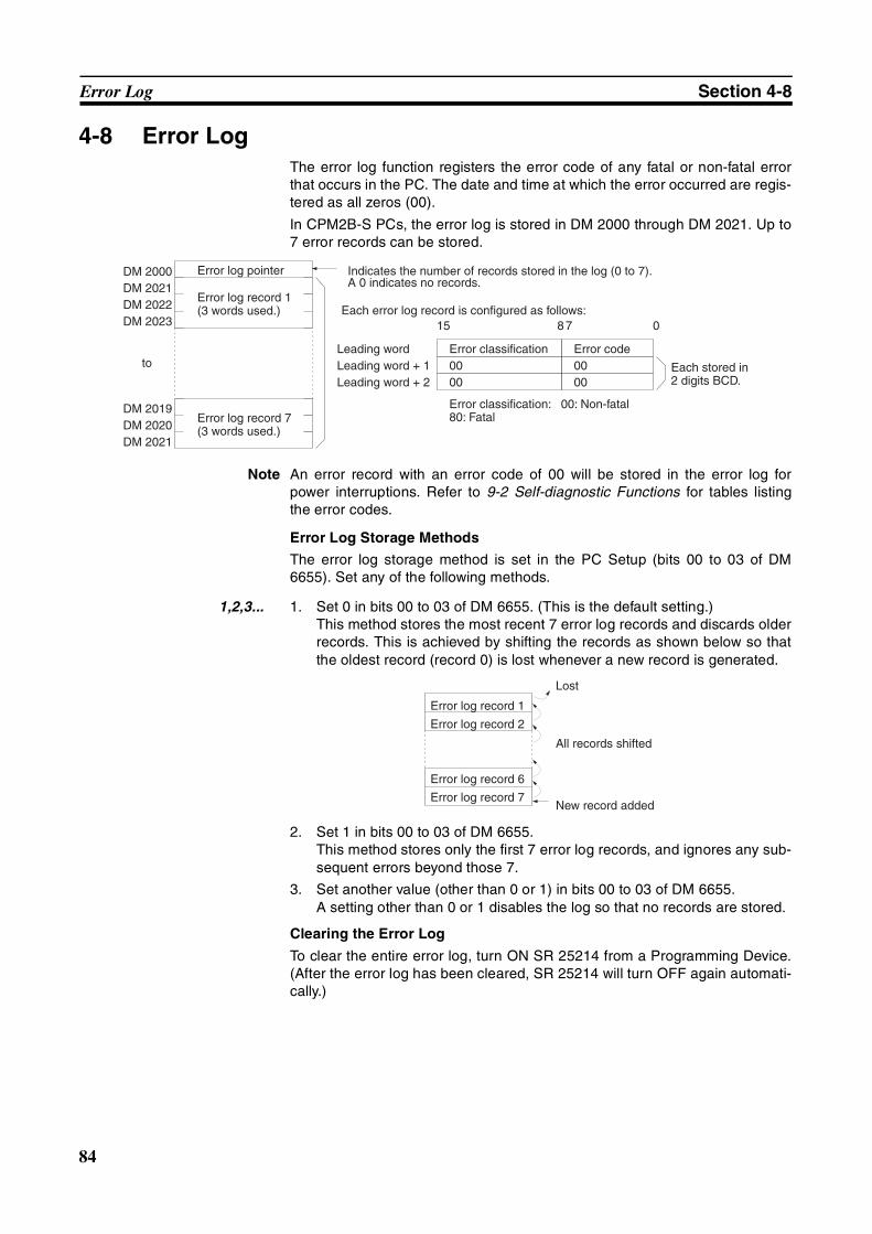
84
Error Log Section 4-8
4-8 Error LogThe error log function registers the error code of any fatal or non-fatal errorthat occurs in the PC. The date and time at which the error occurred are regis-tered as all zeros (00).
In CPM2B-S PCs, the error log is stored in DM 2000 through DM 2021. Up to7 error records can be stored.
Note An error record with an error code of 00 will be stored in the error log forpower interruptions. Refer to 9-2 Self-diagnostic Functions for tables listingthe error codes.
Error Log Storage Methods
The error log storage method is set in the PC Setup (bits 00 to 03 of DM6655). Set any of the following methods.
1,2,3... 1. Set 0 in bits 00 to 03 of DM 6655. (This is the default setting.)This method stores the most recent 7 error log records and discards olderrecords. This is achieved by shifting the records as shown below so thatthe oldest record (record 0) is lost whenever a new record is generated.
2. Set 1 in bits 00 to 03 of DM 6655.This method stores only the first 7 error log records, and ignores any sub-sequent errors beyond those 7.
3. Set another value (other than 0 or 1) in bits 00 to 03 of DM 6655.A setting other than 0 or 1 disables the log so that no records are stored.
Clearing the Error Log
To clear the entire error log, turn ON SR 25214 from a Programming Device.(After the error log has been cleared, SR 25214 will turn OFF again automati-cally.)
DM 2000 Error log pointer
DM 2021Error log record 1 (3 words used.)DM 2022
DM 2023
DM 2019Error log record 7(3 words used.)DM 2020
DM 2021
toError classification Error code00 0000 00
Leading wordLeading word + 1Leading word + 2
Error classification: 00: Non-fatal80: Fatal
Each stored in 2 digits BCD.
15 87 0Each error log record is configured as follows:
Indicates the number of records stored in the log (0 to 7). A 0 indicates no records.
Error log record 6
Error log record 7
Error log record 1
Error log record 2
Lost
New record added
All records shifted

85
SECTION 5Instruction Set
The CPM2B-S PCs have large a programming instruction set that allows for easy programming of complicated controlprocesses. This section provides a brief summary of the instruction set.
5-1 CPM2B-S Function Codes . . . . . . . . . . . . . . . . . . . . . . . . . . . . . . . . . . . . . . . 86
5-2 Alphabetic List by Mnemonic . . . . . . . . . . . . . . . . . . . . . . . . . . . . . . . . . . . . 87
5-3 Expansion Instructions . . . . . . . . . . . . . . . . . . . . . . . . . . . . . . . . . . . . . . . . . . 90
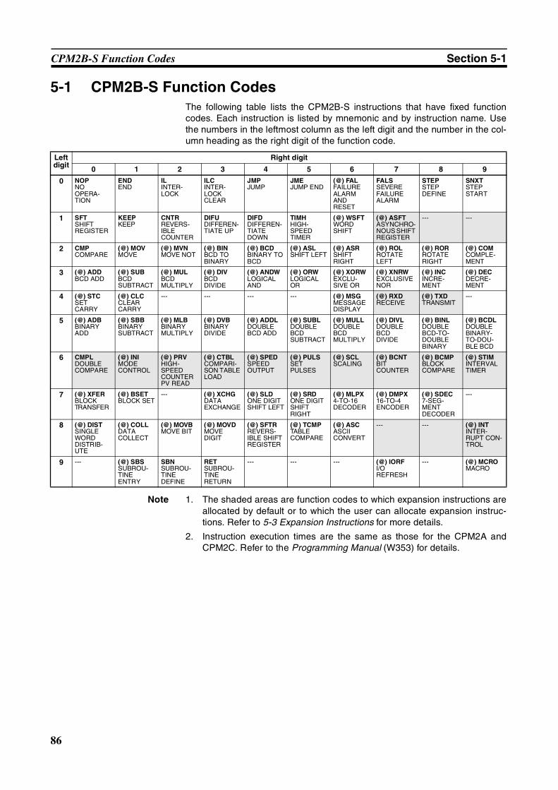
86
CPM2B-S Function Codes Section 5-1
5-1 CPM2B-S Function CodesThe following table lists the CPM2B-S instructions that have fixed functioncodes. Each instruction is listed by mnemonic and by instruction name. Usethe numbers in the leftmost column as the left digit and the number in the col-umn heading as the right digit of the function code.
Note 1. The shaded areas are function codes to which expansion instructions areallocated by default or to which the user can allocate expansion instruc-tions. Refer to 5-3 Expansion Instructions for more details.
2. Instruction execution times are the same as those for the CPM2A andCPM2C. Refer to the Programming Manual (W353) for details.
Left digit
Right digit
0 1 2 3 4 5 6 7 8 9
0 NOPNO OPERA-TION
ENDEND
ILINTER-LOCK
ILCINTER-LOCK CLEAR
JMPJUMP
JMEJUMP END
(@) FALFAILURE ALARM AND RESET
FALSSEVEREFAILURE ALARM
STEPSTEP DEFINE
SNXTSTEP START
1 SFTSHIFT REGISTER
KEEPKEEP
CNTRREVERS-IBLE COUNTER
DIFUDIFFEREN-TIATE UP
DIFDDIFFEREN-TIATE DOWN
TIMHHIGH-SPEED TIMER
(@) WSFTWORD SHIFT
(@) ASFTASYNCHRO-NOUS SHIFT REGISTER
--- ---
2 CMPCOMPARE
(@) MOVMOVE
(@) MVNMOVE NOT
(@) BINBCD TO BINARY
(@) BCDBINARY TO BCD
(@) ASLSHIFT LEFT
(@) ASRSHIFT RIGHT
(@) ROLROTATE LEFT
(@) RORROTATE RIGHT
(@) COMCOMPLE-MENT
3 (@) ADDBCD ADD
(@) SUBBCD SUBTRACT
(@) MULBCD MULTIPLY
(@) DIVBCD DIVIDE
(@) ANDWLOGICAL AND
(@) ORWLOGICAL OR
(@) XORWEXCLU-SIVE OR
(@) XNRWEXCLUSIVE NOR
(@) INCINCRE-MENT
(@) DECDECRE-MENT
4 (@) STCSET CARRY
(@) CLCCLEAR CARRY
--- --- --- --- (@) MSGMESSAGE DISPLAY
(@) RXDRECEIVE
(@) TXDTRANSMIT
---
5 (@) ADBBINARY ADD
(@) SBBBINARY SUBTRACT
(@) MLBBINARY MULTIPLY
(@) DVBBINARY DIVIDE
(@) ADDLDOUBLE BCD ADD
(@) SUBLDOUBLE BCD SUBTRACT
(@) MULLDOUBLE BCD MULTIPLY
(@) DIVLDOUBLE BCD DIVIDE
(@) BINLDOUBLE BCD-TO-DOUBLE BINARY
(@) BCDLDOUBLE BINARY-TO-DOU-BLE BCD
6 CMPLDOUBLE COMPARE
(@) INIMODE CONTROL
(@) PRVHIGH-SPEED COUNTER PV READ
(@) CTBLCOMPARI-SON TABLE LOAD
(@) SPEDSPEED OUTPUT
(@) PULSSET PULSES
(@) SCLSCALING
(@) BCNTBIT COUNTER
(@) BCMPBLOCK COMPARE
(@) STIMINTERVAL TIMER
7 (@) XFERBLOCK TRANSFER
(@) BSETBLOCK SET
--- (@) XCHGDATA EXCHANGE
(@) SLDONE DIGIT SHIFT LEFT
(@) SRDONE DIGIT SHIFT RIGHT
(@) MLPX4-TO-16 DECODER
(@) DMPX16-TO-4 ENCODER
(@) SDEC7-SEG-MENT DECODER
---
8 (@) DISTSINGLE WORD DISTRIB-UTE
(@) COLLDATA COLLECT
(@) MOVBMOVE BIT
(@) MOVDMOVE DIGIT
(@) SFTRREVERS-IBLE SHIFT REGISTER
(@) TCMPTABLE COMPARE
(@) ASCASCII CONVERT
--- --- (@) INTINTER-RUPT CON-TROL
9 --- (@) SBSSUBROU-TINE ENTRY
SBNSUBROU-TINE DEFINE
RETSUBROU-TINE RETURN
--- --- --- (@) IORFI/O REFRESH
--- (@) MCROMACRO
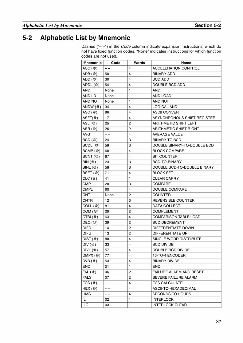
87
Alphabetic List by Mnemonic Section 5-2
5-2 Alphabetic List by MnemonicDashes (“– –”) in the Code column indicate expansion instructions, which donot have fixed function codes. “None” indicates instructions for which functioncodes are not used.
Mnemonic Code Words Name
ACC (@) – – 4 ACCELERATION CONTROL
ADB (@) 50 4 BINARY ADD
ADD (@) 30 4 BCD ADD
ADDL (@) 54 4 DOUBLE BCD ADD
AND None 1 AND
AND LD None 1 AND LOAD
AND NOT None 1 AND NOT
ANDW (@) 34 4 LOGICAL AND
ASC (@) 86 4 ASCII CONVERT
ASFT(@) 17 4 ASYNCHRONOUS SHIFT REGISTER
ASL (@) 25 2 ARITHMETIC SHIFT LEFT
ASR (@) 26 2 ARITHMETIC SHIFT RIGHT
AVG – – 4 AVERAGE VALUE
BCD (@) 24 3 BINARY TO BCD
BCDL (@) 59 3 DOUBLE BINARY-TO-DOUBLE BCD
BCMP (@) 68 4 BLOCK COMPARE
BCNT (@) 67 4 BIT COUNTER
BIN (@) 23 3 BCD-TO-BINARY
BINL (@) 58 3 DOUBLE BCD-TO-DOUBLE BINARY
BSET (@) 71 4 BLOCK SET
CLC (@) 41 1 CLEAR CARRY
CMP 20 3 COMPARE
CMPL 60 4 DOUBLE COMPARE
CNT None 2 COUNTER
CNTR 12 3 REVERSIBLE COUNTER
COLL (@) 81 4 DATA COLLECT
COM (@) 29 2 COMPLEMENT
CTBL(@) 63 4 COMPARISON TABLE LOAD
DEC (@) 39 2 BCD DECREMENT
DIFD 14 2 DIFFERENTIATE DOWN
DIFU 13 2 DIFFERENTIATE UP
DIST (@) 80 4 SINGLE WORD DISTRIBUTE
DIV (@) 33 4 BCD DIVIDE
DIVL (@) 57 4 DOUBLE BCD DIVIDE
DMPX (@) 77 4 16-TO-4 ENCODER
DVB (@) 53 4 BINARY DIVIDE
END 01 1 END
FAL (@) 06 2 FAILURE ALARM AND RESET
FALS 07 2 SEVERE FAILURE ALARM
FCS (@) – – 4 FCS CALCULATE
HEX (@) – – 4 ASCII-TO-HEXADECIMAL
HMS – – 4 SECONDS TO HOURS
IL 02 1 INTERLOCK
ILC 03 1 INTERLOCK CLEAR
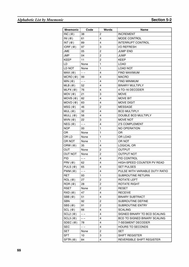
88
Alphabetic List by Mnemonic Section 5-2
INC (@) 38 2 INCREMENT
INI (@) 61 4 MODE CONTROL
INT (@) 89 4 INTERRUPT CONTROL
IORF (@) 97 3 I/O REFRESH
JME 05 2 JUMP END
JMP 04 2 JUMP
KEEP 11 2 KEEP
LD None 1 LOAD
LD NOT None 1 LOAD NOT
MAX (@) – – 4 FIND MAXIMUM
MCRO (@) 99 4 MACRO
MIN (@) – – 4 FIND MINIMUM
MLB (@) 52 4 BINARY MULTIPLY
MLPX (@) 76 4 4-TO-16 DECODER
MOV (@) 21 3 MOVE
MOVB (@) 82 4 MOVE BIT
MOVD (@) 83 4 MOVE DIGIT
MSG (@) 46 2 MESSAGE
MUL (@) 32 4 BCD MULTIPLY
MULL (@) 56 4 DOUBLE BCD MULTIPLY
MVN (@) 22 3 MOVE NOT
NEG (@) – – 4 2’S COMPLEMENT
NOP 00 1 NO OPERATION
OR None 1 OR
OR LD None 1 OR LOAD
OR NOT None 1 OR NOT
ORW (@) 35 4 LOGICAL OR
OUT None 2 OUTPUT
OUT NOT None 2 OUTPUT NOT
PID – – 4 PID CONTROL
PRV (@) 62 4 HIGH-SPEED COUNTER PV READ
PULS (@) 65 4 SET PULSES
PWM (@) – – 4 PULSE WITH VARIABLE DUTY RATIO
RET 93 1 SUBROUTINE RETURN
ROL (@) 27 2 ROTATE LEFT
ROR (@) 28 2 ROTATE RIGHT
RSET None 2 RESET
RXD (@) 47 4 RECEIVE
SBB (@) 51 4 BINARY SUBTRACT
SBN 92 2 SUBROUTINE DEFINE
SBS (@) 91 2 SUBROUTINE ENTRY
SCL (@) 66 4 SCALING
SCL2 (@) – – 4 SIGNED BINARY TO BCD SCALING
SCL3 (@) – – 4 BCD TO SIGNED BINARY SCALING
SDEC (@) 78 4 7-SEGMENT DECODER
SEC – – 4 HOURS TO SECONDS
SET None 2 SET
SFT 10 3 SHIFT REGISTER
SFTR (@) 84 4 REVERSIBLE SHIFT REGISTER
Mnemonic Code Words Name
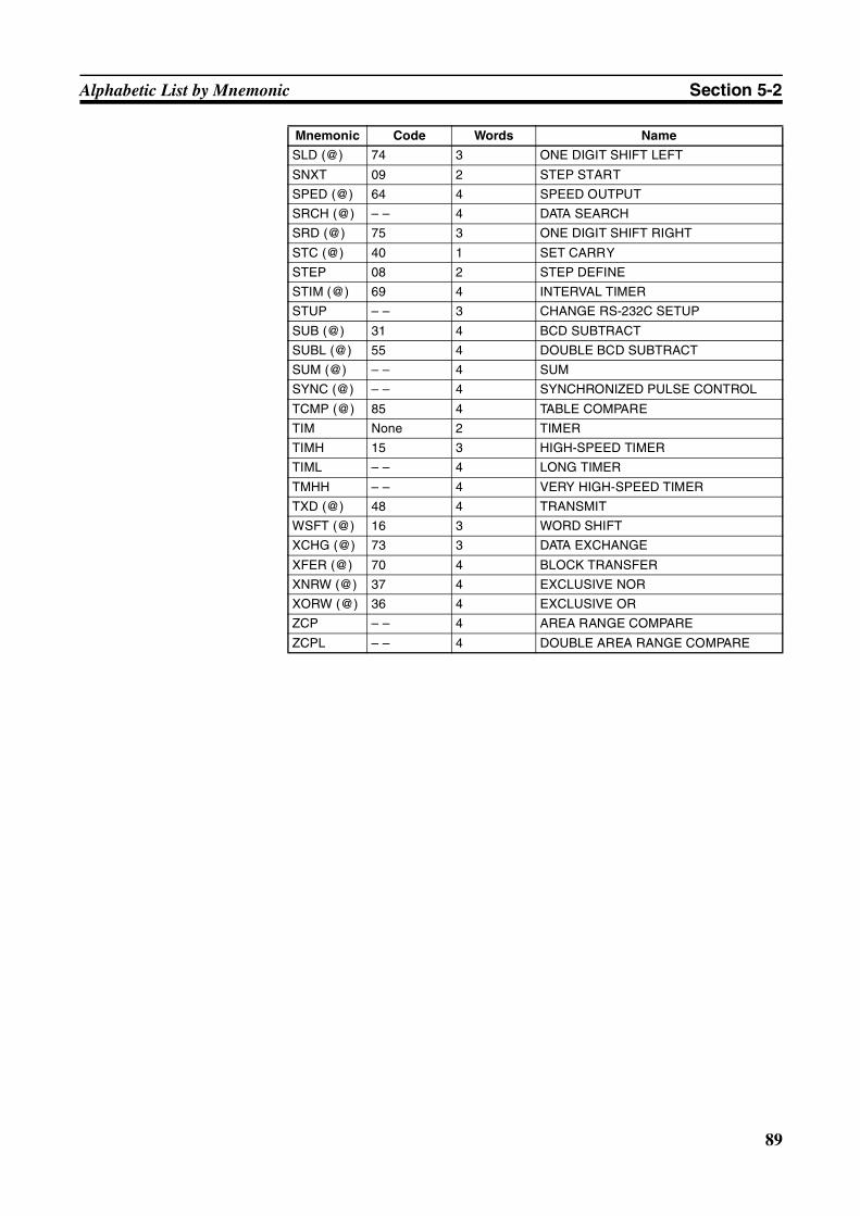
89
Alphabetic List by Mnemonic Section 5-2
SLD (@) 74 3 ONE DIGIT SHIFT LEFT
SNXT 09 2 STEP START
SPED (@) 64 4 SPEED OUTPUT
SRCH (@) – – 4 DATA SEARCH
SRD (@) 75 3 ONE DIGIT SHIFT RIGHT
STC (@) 40 1 SET CARRY
STEP 08 2 STEP DEFINE
STIM (@) 69 4 INTERVAL TIMER
STUP – – 3 CHANGE RS-232C SETUP
SUB (@) 31 4 BCD SUBTRACT
SUBL (@) 55 4 DOUBLE BCD SUBTRACT
SUM (@) – – 4 SUM
SYNC (@) – – 4 SYNCHRONIZED PULSE CONTROL
TCMP (@) 85 4 TABLE COMPARE
TIM None 2 TIMER
TIMH 15 3 HIGH-SPEED TIMER
TIML – – 4 LONG TIMER
TMHH – – 4 VERY HIGH-SPEED TIMER
TXD (@) 48 4 TRANSMIT
WSFT (@) 16 3 WORD SHIFT
XCHG (@) 73 3 DATA EXCHANGE
XFER (@) 70 4 BLOCK TRANSFER
XNRW (@) 37 4 EXCLUSIVE NOR
XORW (@) 36 4 EXCLUSIVE OR
ZCP – – 4 AREA RANGE COMPARE
ZCPL – – 4 DOUBLE AREA RANGE COMPARE
Mnemonic Code Words Name
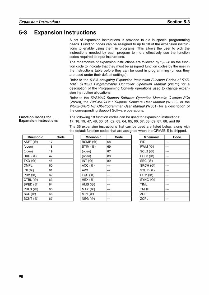
90
Expansion Instructions Section 5-3
5-3 Expansion InstructionsA set of expansion instructions is provided to aid in special programmingneeds. Function codes can be assigned to up to 18 of the expansion instruc-tions to enable using them in programs. This allows the user to pick theinstructions needed by each program to more effectively use the functioncodes required to input instructions.
The mnemonics of expansion instructions are followed by “(– –)” as the func-tion code to indicate that they must be assigned function codes by the user inthe instructions table before they can be used in programming (unless theyare used under their default settings).
Refer to the 6-2-5 Assigning Expansion Instruction Function Codes of SYS-MAC CPM2B Programmable Controller Operation Manual (W371) for adescription of the Programming Console operations used to change expan-sion instruction allocations.
Refer to the SYSMAC Support Software Operation Manuals: C-series PCs(W248), the SYSMAC-CPT Support Software User Manual (W333), or theWS02-CXPC1-E CX-Programmer User Manual (W361) for a description ofthe corresponding Support Software operations.
Function Codes for Expansion Instructions
The following 18 function codes can be used for expansion instructions:17, 18, 19, 47, 48, 60, 61, 62, 63, 64, 65, 66, 67, 68, 69, 87, 88, and 89
The 35 expansion instructions that can be used are listed below, along withthe default function codes that are assigned when the CPM2B-S is shipped.
Mnemonic Code Mnemonic Code Mnemonic Code
ASFT (@) 17 BCMP (@) 68 PID ---
(open) 18 STIM (@) 69 PWM (@) ---
(open) 19 (open) 87 SCL2 (@) ---
RXD (@) 47 (open) 88 SCL3 (@) ---
TXD (@) 48 INT (@) 89 SEC (@) ---
CMPL 60 ACC (@) --- SRCH (@) ---
INI (@) 61 AVG --- STUP (@) ---
PRV (@) 62 FCS (@) --- SUM (@) ---
CTBL (@) 63 HEX (@) --- SYNC (@) ---
SPED (@) 64 HMS (@) --- TIML ---
PULS (@) 65 MAX (@) --- TMHH ---
SCL (@) 66 MIN (@) --- ZCP ---
BCNT (@) 67 NEG (@) --- ZCPL ---
91
SECTION 6Exchanging Data with CompoBus/S Slaves
This section explains how to exchange data with CompoBus/S Slaves when using the CPM2B-S as a CompoBus/S Master.Read this section when using CompoBus/S I/O link communications.
6-1 Initial Settings . . . . . . . . . . . . . . . . . . . . . . . . . . . . . . . . . . . . . . . . . . . . . . . . . 92
6-1-1 Setting the Maximum Number of Nodes . . . . . . . . . . . . . . . . . . . . . 92
6-1-2 Setting the CompoBus/S Communications Mode . . . . . . . . . . . . . . 92
6-2 Remote I/O Communications . . . . . . . . . . . . . . . . . . . . . . . . . . . . . . . . . . . . . 93
6-2-1 Slaves . . . . . . . . . . . . . . . . . . . . . . . . . . . . . . . . . . . . . . . . . . . . . . . . 93
6-2-2 I/O Allocation . . . . . . . . . . . . . . . . . . . . . . . . . . . . . . . . . . . . . . . . . . 94
6-3 Communications Status. . . . . . . . . . . . . . . . . . . . . . . . . . . . . . . . . . . . . . . . . . 95
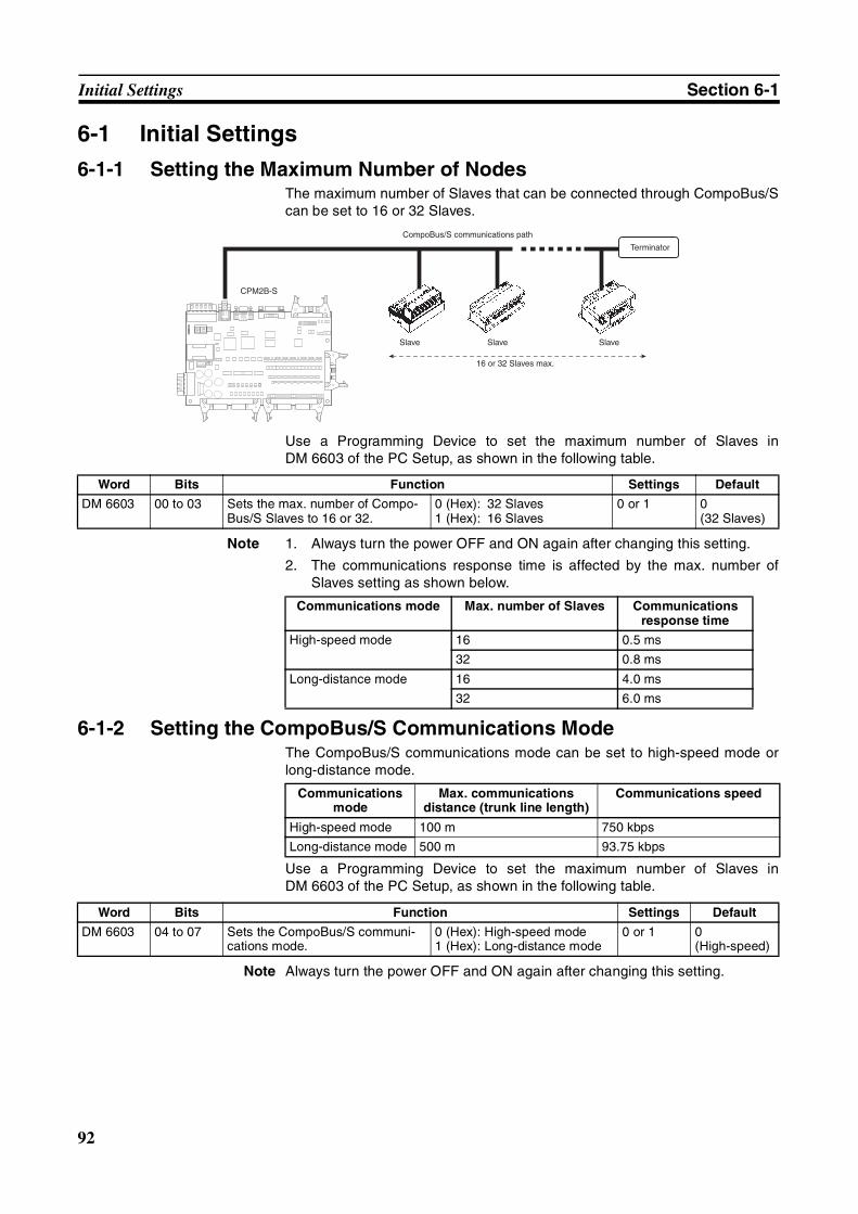
92
Initial Settings Section 6-1
6-1 Initial Settings
6-1-1 Setting the Maximum Number of NodesThe maximum number of Slaves that can be connected through CompoBus/Scan be set to 16 or 32 Slaves.
Use a Programming Device to set the maximum number of Slaves inDM 6603 of the PC Setup, as shown in the following table.
Note 1. Always turn the power OFF and ON again after changing this setting.
2. The communications response time is affected by the max. number ofSlaves setting as shown below.
6-1-2 Setting the CompoBus/S Communications ModeThe CompoBus/S communications mode can be set to high-speed mode orlong-distance mode.
Use a Programming Device to set the maximum number of Slaves inDM 6603 of the PC Setup, as shown in the following table.
Note Always turn the power OFF and ON again after changing this setting.
CompoBus/S communications path
Terminator
Slave Slave Slave
16 or 32 Slaves max.
CPM2B-S
Word Bits Function Settings Default
DM 6603 00 to 03 Sets the max. number of Compo-Bus/S Slaves to 16 or 32.
0 (Hex): 32 Slaves1 (Hex): 16 Slaves
0 or 1 0(32 Slaves)
Communications mode Max. number of Slaves Communications response time
High-speed mode 16 0.5 ms
32 0.8 ms
Long-distance mode 16 4.0 ms
32 6.0 ms
Communications mode
Max. communications distance (trunk line length)
Communications speed
High-speed mode 100 m 750 kbps
Long-distance mode 500 m 93.75 kbps
Word Bits Function Settings Default
DM 6603 04 to 07 Sets the CompoBus/S communi-cations mode.
0 (Hex): High-speed mode1 (Hex): Long-distance mode
0 or 1 0(High-speed)
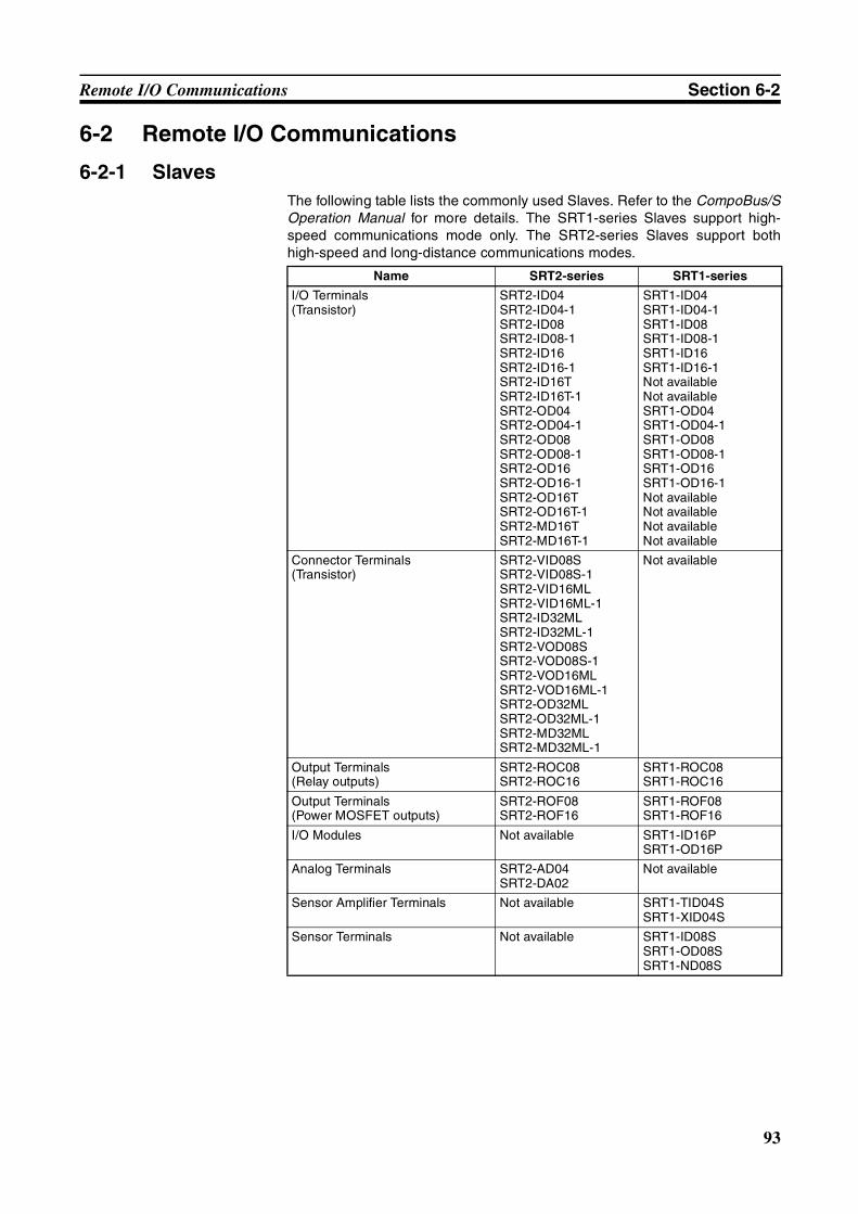
93
Remote I/O Communications Section 6-2
6-2 Remote I/O Communications
6-2-1 SlavesThe following table lists the commonly used Slaves. Refer to the CompoBus/SOperation Manual for more details. The SRT1-series Slaves support high-speed communications mode only. The SRT2-series Slaves support bothhigh-speed and long-distance communications modes.
Name SRT2-series SRT1-series
I/O Terminals(Transistor)
SRT2-ID04SRT2-ID04-1SRT2-ID08SRT2-ID08-1SRT2-ID16SRT2-ID16-1SRT2-ID16TSRT2-ID16T-1SRT2-OD04SRT2-OD04-1SRT2-OD08SRT2-OD08-1SRT2-OD16SRT2-OD16-1SRT2-OD16TSRT2-OD16T-1SRT2-MD16TSRT2-MD16T-1
SRT1-ID04SRT1-ID04-1SRT1-ID08SRT1-ID08-1SRT1-ID16SRT1-ID16-1Not availableNot availableSRT1-OD04SRT1-OD04-1SRT1-OD08SRT1-OD08-1SRT1-OD16SRT1-OD16-1Not availableNot availableNot availableNot available
Connector Terminals(Transistor)
SRT2-VID08SSRT2-VID08S-1SRT2-VID16MLSRT2-VID16ML-1SRT2-ID32MLSRT2-ID32ML-1SRT2-VOD08SSRT2-VOD08S-1SRT2-VOD16MLSRT2-VOD16ML-1SRT2-OD32MLSRT2-OD32ML-1SRT2-MD32MLSRT2-MD32ML-1
Not available
Output Terminals(Relay outputs)
SRT2-ROC08SRT2-ROC16
SRT1-ROC08SRT1-ROC16
Output Terminals(Power MOSFET outputs)
SRT2-ROF08SRT2-ROF16
SRT1-ROF08SRT1-ROF16
I/O Modules Not available SRT1-ID16PSRT1-OD16P
Analog Terminals SRT2-AD04SRT2-DA02
Not available
Sensor Amplifier Terminals Not available SRT1-TID04SSRT1-XID04S
Sensor Terminals Not available SRT1-ID08SSRT1-OD08SSRT1-ND08S
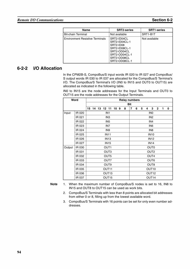
94
Remote I/O Communications Section 6-2
6-2-2 I/O AllocationIn the CPM2B-S, CompoBus/S input words IR 020 to IR 027 and CompoBus/S output words IR 030 to IR 037 are allocated for the CompoBus/S Terminal’sI/O. The CompoBus/S Terminal’s I/O (IN0 to IN15 and OUT0 to OUT15) areallocated as indicated in the following table.
IN0 to IN15 are the node addresses for the Input Terminals and OUT0 toOUT15 are the node addresses for the Output Terminals.
Note 1. When the maximum number of CompoBus/S nodes is set to 16, IN8 toIN15 and OUT8 to OUT15 can be used as work bits.
2. CompoBus/S Terminals with less than 8 points are allocated bit addressesfrom either 0 or 8, filling up from the lowest available word.
3. CompoBus/S Terminals with 16 points can be set for only even number ad-dresses.
Bit-chain Terminal Not available SRT1-B1T
Environment Resistive Terminals SRT2-ID04CLSRT2-ID04CL-1SRT2-ID08SRT2-ID08CL-1SRT2-OD04CLSRT2-OD04CL-1SRT2-OD08CLSRT2-OD08CL-1
Not available
Name SRT2-series SRT1-series
Word Relay numbers
Bit
15 14 13 12 11 10 9 8 7 6 5 4 3 2 1 0
Input IR 020 IN1 IN0
IR 021 IN3 IN2
IR 022 IN5 IN4
IR 023 IN7 IN6
IR 024 IN9 IN8
IR 025 IN11 IN10
IR 026 IN13 IN12
IR 027 IN15 IN14
Output IR 030 OUT1 OUT0
IR 031 OUT3 OUT2
IR 032 OUT5 OUT4
IR 033 OUT7 OUT6
IR 034 OUT9 OUT8
IR 035 OUT11 OUT10
IR 036 OUT13 OUT12
IR 037 OUT15 OUT14
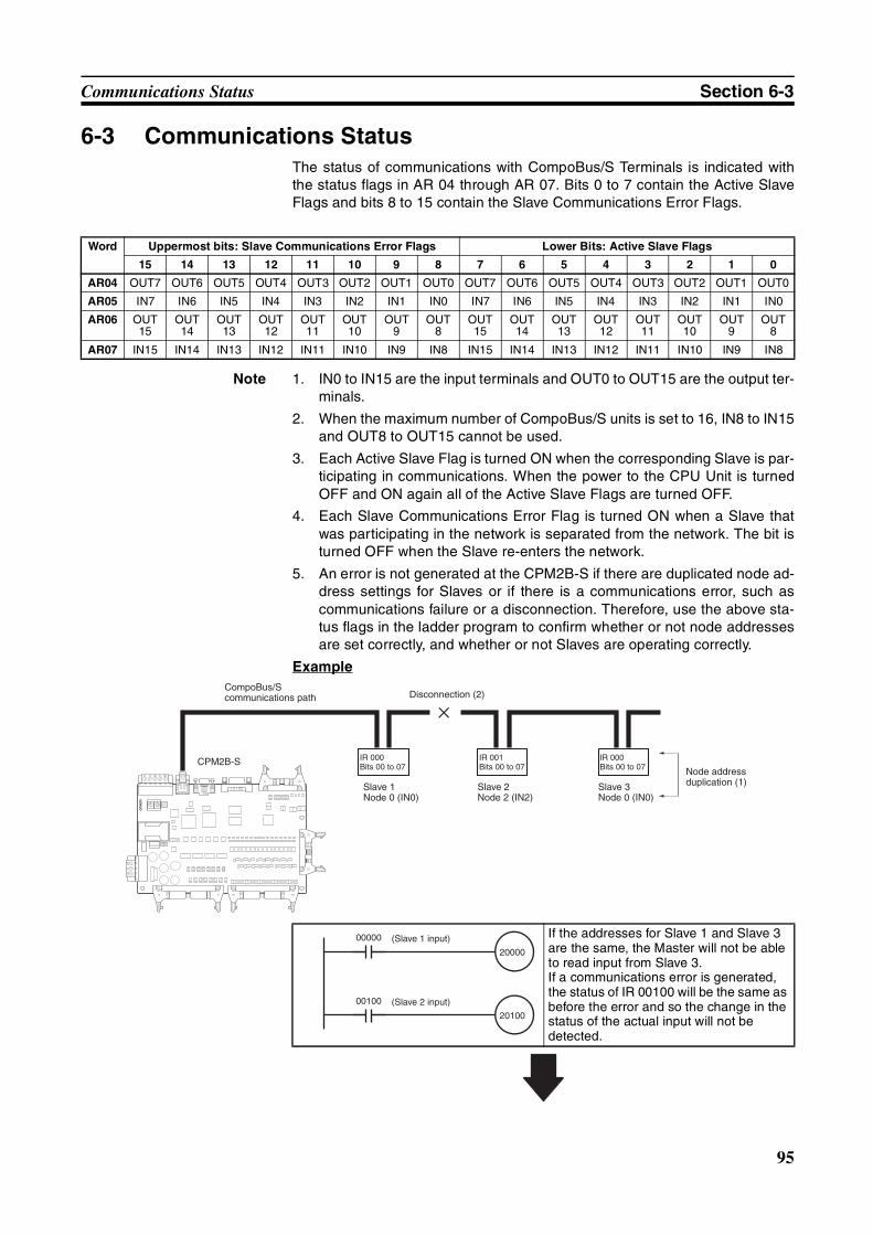
95
Communications Status Section 6-3
6-3 Communications StatusThe status of communications with CompoBus/S Terminals is indicated withthe status flags in AR 04 through AR 07. Bits 0 to 7 contain the Active SlaveFlags and bits 8 to 15 contain the Slave Communications Error Flags.
Note 1. IN0 to IN15 are the input terminals and OUT0 to OUT15 are the output ter-minals.
2. When the maximum number of CompoBus/S units is set to 16, IN8 to IN15and OUT8 to OUT15 cannot be used.
3. Each Active Slave Flag is turned ON when the corresponding Slave is par-ticipating in communications. When the power to the CPU Unit is turnedOFF and ON again all of the Active Slave Flags are turned OFF.
4. Each Slave Communications Error Flag is turned ON when a Slave thatwas participating in the network is separated from the network. The bit isturned OFF when the Slave re-enters the network.
5. An error is not generated at the CPM2B-S if there are duplicated node ad-dress settings for Slaves or if there is a communications error, such ascommunications failure or a disconnection. Therefore, use the above sta-tus flags in the ladder program to confirm whether or not node addressesare set correctly, and whether or not Slaves are operating correctly.
Example
Word Uppermost bits: Slave Communications Error Flags Lower Bits: Active Slave Flags
15 14 13 12 11 10 9 8 7 6 5 4 3 2 1 0
AR04 OUT7 OUT6 OUT5 OUT4 OUT3 OUT2 OUT1 OUT0 OUT7 OUT6 OUT5 OUT4 OUT3 OUT2 OUT1 OUT0
AR05 IN7 IN6 IN5 IN4 IN3 IN2 IN1 IN0 IN7 IN6 IN5 IN4 IN3 IN2 IN1 IN0
AR06 OUT15
OUT14
OUT13
OUT12
OUT11
OUT10
OUT9
OUT8
OUT15
OUT14
OUT13
OUT12
OUT11
OUT10
OUT9
OUT8
AR07 IN15 IN14 IN13 IN12 IN11 IN10 IN9 IN8 IN15 IN14 IN13 IN12 IN11 IN10 IN9 IN8
If the addresses for Slave 1 and Slave 3 are the same, the Master will not be able to read input from Slave 3.If a communications error is generated, the status of IR 00100 will be the same as before the error and so the change in the status of the actual input will not be detected.
Slave 3Node 0 (IN0)
Slave 2Node 2 (IN2)
Slave 1Node 0 (IN0)
Node address duplication (1)
IR 000Bits 00 to 07
IR 001Bits 00 to 07
IR 000Bits 00 to 07
CompoBus/Scommunications path Disconnection (2)
CPM2B-S
20000
00000
20100
00100
(Slave 1 input)
(Slave 2 input)
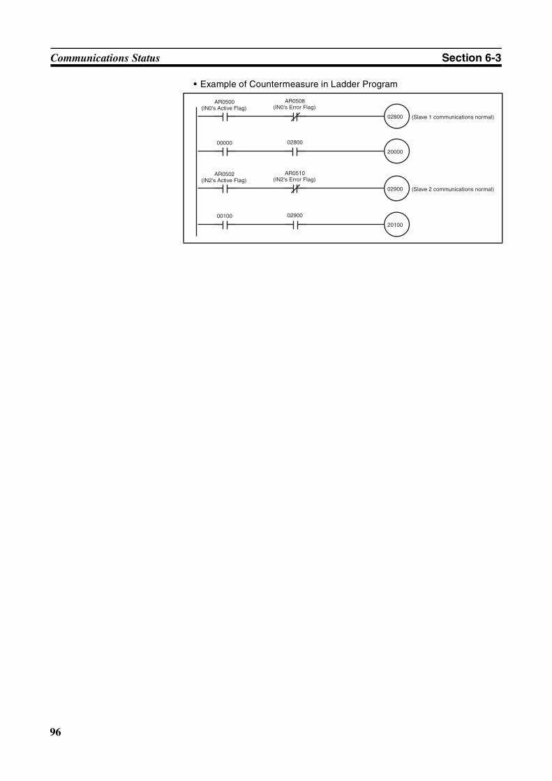
96
Communications Status Section 6-3
• Example of Countermeasure in Ladder Program
02800
AR0500(IN0's Error Flag)(IN0's Active Flag)
AR0508
(Slave 1 communications normal)
20000
00000 02800
02900
AR0502(IN2's Error Flag)(IN2's Active Flag)
AR0510
(Slave 2 communications normal)
20100
00100 02900
97
SECTION 7Exchanging Data with a DeviceNet Master
This section explains how data is exchanged between the CPM2B-S100M-DRT and a DeviceNet Master. Refer to thissection when using remote I/O communications or explicit message communications from a DeviceNet Master.
7-1 Initial Settings . . . . . . . . . . . . . . . . . . . . . . . . . . . . . . . . . . . . . . . . . . . . . . . . . 98
7-1-1 Setting the Node Number . . . . . . . . . . . . . . . . . . . . . . . . . . . . . . . . . 98
7-1-2 Setting the Communications Speed . . . . . . . . . . . . . . . . . . . . . . . . . 98
7-1-3 Attaching Status Information . . . . . . . . . . . . . . . . . . . . . . . . . . . . . . 98
7-2 Remote I/O Communications . . . . . . . . . . . . . . . . . . . . . . . . . . . . . . . . . . . . . 98
7-3 Explicit Message Communications. . . . . . . . . . . . . . . . . . . . . . . . . . . . . . . . . 101
7-3-1 DeviceNet Explicit Message Functions . . . . . . . . . . . . . . . . . . . . . . 101
7-3-2 Command and Response Formats . . . . . . . . . . . . . . . . . . . . . . . . . . 102
7-3-3 Examples of DeviceNet Explicit Messages . . . . . . . . . . . . . . . . . . . 108
7-4 Status Information. . . . . . . . . . . . . . . . . . . . . . . . . . . . . . . . . . . . . . . . . . . . . . 113
7-4-1 LED Indicators . . . . . . . . . . . . . . . . . . . . . . . . . . . . . . . . . . . . . . . . . 113
7-4-2 AR Area Flags indicating DeviceNet Status. . . . . . . . . . . . . . . . . . . 114
7-4-3 CPM2B-S Status Output to DeviceNet. . . . . . . . . . . . . . . . . . . . . . . 114
98
Initial Settings Section 7-1
7-1 Initial Settings
7-1-1 Setting the Node NumberSet the DeviceNet node number with the rotary switches on the CPM2B-SCPU Board. The allowed setting range is 00 to 63; node number settings 64 to99 are not allowed. The rotary switch settings are read when the Unit’s poweris turned ON.
7-1-2 Setting the Communications SpeedSet the DeviceNet communications speed with DIP switch 2 on the front of theUnit. The DIP switch settings are read when the Unit’s power is turned ON.
7-1-3 Attaching Status InformationIt is possible to enable and disable the attachment of the CPM2B-S statusinformation in transmissions from the CPM2B-S to the Master Unit.
The status attachment is set in DM 6605 of the PC Setup, as shown in the fol-lowing table. The initial setting is 0 (attach status information); change thissetting to 1 to disable attachment of status information. Refer to 7-4 StatusInformation for details on the status information.
7-2 Remote I/O CommunicationsAllocate the DeviceNet read and write areas to specify what part of the PC’sdata area will be used to read and write data from the DeviceNet Master Unit.Specify the PC data area, starting word address, and number of bytes. Up to64 bytes can be allocated for DeviceNet remote I/O.
Allocating Read/Write Areas with the PC Setup
Switch the CPM2B-S to PROGRAM mode and use a Programming Device,such as a Programming Console or Support Software, to make the followingsettings in DM 6605 to DM 6609 of the PC Setup. The settings in these wordsare read only when the CPM2B-S is turned ON, so the PC’s power must beturned OFF and then ON again to make changes effective.
X10 X1
DIP switch 2 settings DeviceNet communications speed
Maximum total communications distancePin 1 Pin 2
OFF OFF 125 kbps 500 m max.
ON OFF 250 kbps 250 m max.
OFF ON 500 kbps 100 m max.
ON ON Not used. ---
ON
Word Bits Function DefaultDM 6605 04 to 07 Sets whether CPM2B-S status is transmitted to
the DeviceNet Master.
0 (Hex): Attach status ahead of data.1 (Hex): Do not attach status ahead of data.
0(Attach status.)
99
Remote I/O Communications Section 7-2
Note 1. A system failure error (PC Setup setting error) will occur if the number ofbytes is set to 00 (Hex) for both the write and read areas.
2. Data written through DeviceNet is valid even if the PC is in PROGRAMmode, so outputs may go ON when the PC is in PROGRAM mode if outputbits are allocated to the DeviceNet I/O Link Write area. To prevent outputsfrom going ON while the PC is in PROGRAM mode, do not allocate outputbits directly to the DeviceNet I/O Link Write area.
3. If words in any areas other than the IR area (IR 000 to IR 227) or LR area(LR 00 to LR 15) are allocated to the I/O Link Read area, the data may notbe cleared even when the power is interrupted, possibly causing data fromimmediately before power interruption to be read by the master. If this cre-ates a potential problem, use the following measures to eliminate the prob-lem.
• When starting in RUN or MONITOR mode, configure the ladder pro-gram so that the Read area is rewritten with appropriate data.
• When starting in PROGRAM mode, it will not be possible to take directmeasures at the slave. Monitor the status at the master and do notread the data when the operating mode is PROGRAM mode.
When a fatal error occurs at a slave, the master may read data from imme-diately before the error. In this case also, monitor the status at the masterand do not read the data.
Word Bits Function DefaultDM 6605 00 to 03 DeviceNet Read/Write area setting
0 (Hex): Read (IN) IR 020 to IR 027; Write (OUT) IR 030 to IR 0371 (Hex): Use settings in DM 6606 to DM 6609.
0 (Hex)
04 to 07 Transmission of CPM2B-S status to the DeviceNet Master
0 (Hex): Attach status information ahead of data.1 (Hex): Do not attach status information ahead of data.
0 (Hex)
08 to 15 Not used. 0 (Hex)
DM 6606 00 to 07 DeviceNet I/O Link Write (OUT) area settings
(Master → CPM2B-S)
Data area
01 (Hex): I/O area 1 (IR 000 to IR 049)02 (Hex): I/O area 2 (IR 200 to IR 227)03 (Hex): DM area (DM 0000 to DM 2047)04 (Hex): LR area (LR 00 to LR 15)05 (Hex): HR area (HR 00 to HR 19)07 (Hex): Timer/counter area (TC 000 to TC 255)
00 (Hex)
08 to 15 Number of bytes (see note 1)
01 to 40 (Hex) (equivalent to 0 to 64 decimal)
00 (Hex)
DM 6607 00 to 15 Starting word address
0000 to 07FF (Hex) (equivalent to 0000 to 2047 decimal)
0000 (Hex)
DM 6608 00 to 07 DeviceNet I/O Link Read (IN) area settings
(CPM2B-S → Master)
Data area
01 (Hex): I/O area 1 (IR 000 to IR 049)02 (Hex): I/O area 2 (IR 200 to IR 227)03 (Hex): DM area (DM 0000 to DM 2047)04 (Hex): LR area (LR 00 to LR 15)05 (Hex): HR area (HR 00 to HR 19)06 (Hex): AR area (AR 00 to AR 23)07 (Hex): Timer/counter area (TC 000 to TC 255)
00 (Hex)
08 to 15 Number of bytes (see note 1)
01 to 40 (Hex) (equivalent to 0 to 64 decimal)
00 (Hex)
DM 6609 00 to 15 Starting word address
0000 to 07FF (Hex) (equivalent to 0000 to 2047 decimal)
0000 (Hex)
100
Remote I/O Communications Section 7-2
Allocating Read/Write Areas with the DeviceNet Configurator
An OMRON DeviceNet Configurator (version 2.0 or higher) can be used tospecify the DeviceNet Read and Write areas. Contact your OMRON repre-sentative if you are using a Configurator version earlier than 2.0. (The versioncan be displayed in the Configurator’s Help menu.)
1,2,3... 1. Connect the DeviceNet Configurator to the DeviceNet network and switchto online operation.
2. Turn ON the CPM2B-S power supply and put the PC in PROGRAM mode.
3. Click the Upload Button.
4. Double-click the CPM2B-S to be set on the DeviceNet Configurator’s de-vice list.
5. The DeviceNet Parameters Window will be displayed to edit the read andwrite area parameters. Double-click the read/write area parameters to bechanged.
6. Change the parameters as shown in the following example.
101
Explicit Message Communications Section 7-3
a) Double-click the parameter to be changed.
b) Enter the desired value and press the Enter Key.
7. When all parameters are set as required, click the Download Button.
8. After the download has been completed, click the OK Button to return tothe list display.
7-3 Explicit Message Communications
7-3-1 DeviceNet Explicit Message FunctionsExplicit message communications use a command/response protocol. TheCPM2B-S returns responses to commands sent from the Master, allowingCPM2B-S data areas to be read or written from the Master.
CPM2B-S)
DeviceNet Master
Command message
Response message
CPM2B-S
102
Explicit Message Communications Section 7-3
Explicit Message List
Note 1. When sending explicit message commands, the range of data specified bythe data area, starting address, and number of bytes must not exceed therange of the CPM2B-S data area.
2. Use the READ BYTE DATA and WRITE BYTE DATA commands whensending explicit message commands from an OMRON DeviceNet Master.
Use the READ WORD DATA and WRITE WORD DATA commands whensending explicit message commands from another company’s DeviceNetMaster.
3. The number of bytes occupied by the “Class ID” and “Instance ID” param-eters varies from Master to Master. These parameters are specified in 2bytes (4 digits) in commands sent from OMRON DeviceNet Masters. (CV-series PCs use the CMND instruction and C200HX/HG/HE PCs use theIOWR instruction.)
7-3-2 Command and Response FormatsREAD BYTE DATA Reads the specified node’s data in byte-units from the DeviceNet Master.
When word data is being read, the leftmost byte is read before the rightmostbyte. Up to 200 bytes can be read at one time.
Command Format
Explicit message Function PageREAD BYTE DATA Reads the specified node’s data in byte-units from
the DeviceNet Master. When word data is being read, the leftmost byte is read before the rightmost byte. Up to 200 bytes can be read at one time.
102
WRITE BYTE DATA Writes data from the DeviceNet Master to the speci-fied node’s data area in byte-units. When word data is being written, the leftmost byte is written before the rightmost byte. Up to 200 bytes can be written at one time.
104
READ WORD DATA Reads the specified node’s data in word-units (two-byte units) from the DeviceNet Master. When word data is being read, the leftmost byte is read before the rightmost byte. Up to 100 words can be read at one time.
105
WRITE WORD DATA Writes data from the DeviceNet Master to the speci-fied node’s data area in word-units (two-byte units). When word data is being written, the leftmost byte is written before the rightmost byte. Up to 100 words can be written at one time.
106
ERROR RESPONSE The CPM2B-S returns an error response when there is an error in the explicit message command sent from the DeviceNet Master.
108
Destination node number
Service code
Class ID
Instance ID
Address L
Address H
Number of bytes
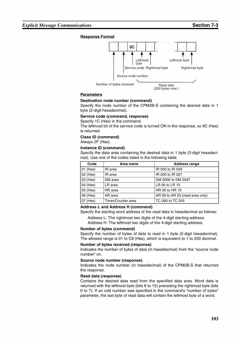
103
Explicit Message Communications Section 7-3
Response Format
Parameters
Destination node number (command)Specify the node number of the CPM2B-S containing the desired data in 1byte (2-digit hexadecimal).
Service code (command, response)Specify 1C (Hex) in the command.The leftmost bit of the service code is turned ON in the response, so 9C (Hex)is returned.
Class ID (command)Always 2F (Hex).
Instance ID (command)Specify the data area containing the desired data in 1 byte (2-digit hexadeci-mal). Use one of the codes listed in the following table.
Address L and Address H (command)Specify the starting word address of the read data in hexadecimal as follows:
Address L: The rightmost two digits of the 4-digit starting address.Address H: The leftmost two digits of the 4-digit starting address.
Number of bytes (command)Specify the number of bytes of data to read in 1 byte (2-digit hexadecimal).The allowed range is 01 to C8 (Hex), which is equivalent to 1 to 200 decimal.
Number of bytes received (response)Indicates the number of bytes of data (in hexadecimal) from the “source nodenumber” on.
Source node number (response)Indicates the node number (in hexadecimal) of the CPM2B-S that returnedthe response.
Read data (response)Contains the desired data read from the specified data area. Word data isreturned with the leftmost byte (bits 8 to 15) preceding the rightmost byte (bits0 to 7). If an odd number was specified in the command’s “number of bytes”parameter, the last byte of read data will contain the leftmost byte of a word.
Code Area name Address range01 (Hex) IR area IR 000 to IR 049
02 (Hex) IR area IR 200 to IR 227
03 (Hex) DM area DM 0000 to DM 2047
04 (Hex) LR area LR 00 to LR 15
05 (Hex) HR area HR 00 to HR 19
06 (Hex) AR area AR 00 to AR 23 (read area only)
07 (Hex) Timer/Counter area TC 000 to TC 255
Number of bytes received
Source node number
Service code
Leftmost byte
Rightmost byte
Read data(200 bytes max.)
Leftmost byte
Rightmost byte
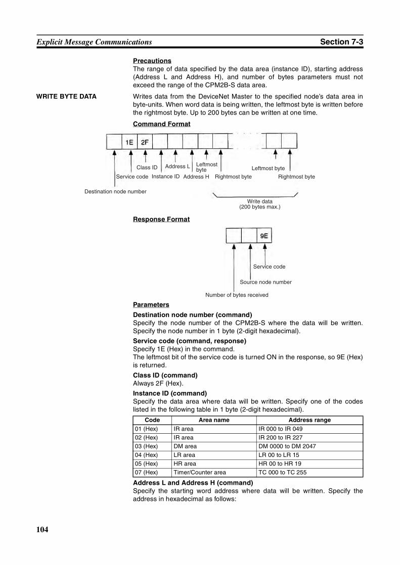
104
Explicit Message Communications Section 7-3
PrecautionsThe range of data specified by the data area (instance ID), starting address(Address L and Address H), and number of bytes parameters must notexceed the range of the CPM2B-S data area.
WRITE BYTE DATA Writes data from the DeviceNet Master to the specified node’s data area inbyte-units. When word data is being written, the leftmost byte is written beforethe rightmost byte. Up to 200 bytes can be written at one time.
Command Format
Response Format
Parameters
Destination node number (command)Specify the node number of the CPM2B-S where the data will be written.Specify the node number in 1 byte (2-digit hexadecimal).
Service code (command, response)Specify 1E (Hex) in the command.The leftmost bit of the service code is turned ON in the response, so 9E (Hex)is returned.
Class ID (command)Always 2F (Hex).
Instance ID (command)Specify the data area where data will be written. Specify one of the codeslisted in the following table in 1 byte (2-digit hexadecimal).
Address L and Address H (command)Specify the starting word address where data will be written. Specify theaddress in hexadecimal as follows:
Destination node number
Service code
Class ID
Instance ID
Address L
Address H
Leftmost byte
Rightmost byte
Write data(200 bytes max.)
Leftmost byte
Rightmost byte
Code Area name Address range01 (Hex) IR area IR 000 to IR 049
02 (Hex) IR area IR 200 to IR 227
03 (Hex) DM area DM 0000 to DM 2047
04 (Hex) LR area LR 00 to LR 15
05 (Hex) HR area HR 00 to HR 19
07 (Hex) Timer/Counter area TC 000 to TC 255
Number of bytes received
Source node number
Service code
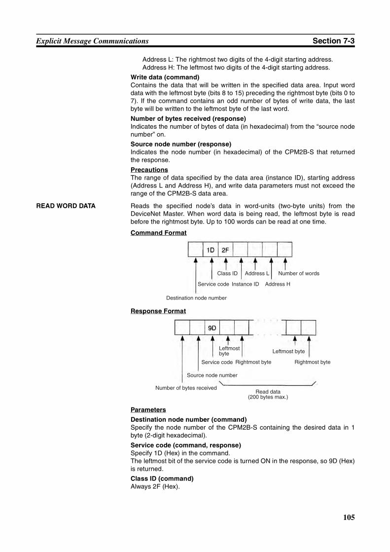
105
Explicit Message Communications Section 7-3
Address L: The rightmost two digits of the 4-digit starting address.Address H: The leftmost two digits of the 4-digit starting address.
Write data (command)Contains the data that will be written in the specified data area. Input worddata with the leftmost byte (bits 8 to 15) preceding the rightmost byte (bits 0 to7). If the command contains an odd number of bytes of write data, the lastbyte will be written to the leftmost byte of the last word.
Number of bytes received (response)Indicates the number of bytes of data (in hexadecimal) from the “source nodenumber” on.
Source node number (response)Indicates the node number (in hexadecimal) of the CPM2B-S that returnedthe response.
PrecautionsThe range of data specified by the data area (instance ID), starting address(Address L and Address H), and write data parameters must not exceed therange of the CPM2B-S data area.
READ WORD DATA Reads the specified node’s data in word-units (two-byte units) from theDeviceNet Master. When word data is being read, the leftmost byte is readbefore the rightmost byte. Up to 100 words can be read at one time.
Command Format
Response Format
Parameters
Destination node number (command)Specify the node number of the CPM2B-S containing the desired data in 1byte (2-digit hexadecimal).
Service code (command, response)Specify 1D (Hex) in the command.The leftmost bit of the service code is turned ON in the response, so 9D (Hex)is returned.
Class ID (command)Always 2F (Hex).
Destination node number
Service code
Class ID
Instance ID
Address L
Address H
Number of words
Number of bytes received
Source node number
Service code
Leftmost byte
Rightmost byte
Read data(200 bytes max.)
Leftmost byte
Rightmost byte
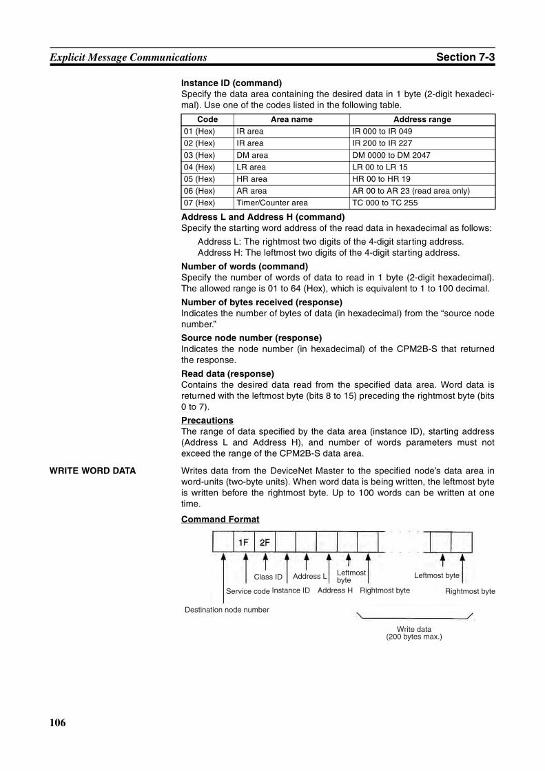
106
Explicit Message Communications Section 7-3
Instance ID (command)Specify the data area containing the desired data in 1 byte (2-digit hexadeci-mal). Use one of the codes listed in the following table.
Address L and Address H (command)Specify the starting word address of the read data in hexadecimal as follows:
Address L: The rightmost two digits of the 4-digit starting address.Address H: The leftmost two digits of the 4-digit starting address.
Number of words (command)Specify the number of words of data to read in 1 byte (2-digit hexadecimal).The allowed range is 01 to 64 (Hex), which is equivalent to 1 to 100 decimal.
Number of bytes received (response)Indicates the number of bytes of data (in hexadecimal) from the “source nodenumber.”
Source node number (response)Indicates the node number (in hexadecimal) of the CPM2B-S that returnedthe response.
Read data (response)Contains the desired data read from the specified data area. Word data isreturned with the leftmost byte (bits 8 to 15) preceding the rightmost byte (bits0 to 7).
PrecautionsThe range of data specified by the data area (instance ID), starting address(Address L and Address H), and number of words parameters must notexceed the range of the CPM2B-S data area.
WRITE WORD DATA Writes data from the DeviceNet Master to the specified node’s data area inword-units (two-byte units). When word data is being written, the leftmost byteis written before the rightmost byte. Up to 100 words can be written at onetime.
Command Format
Code Area name Address range01 (Hex) IR area IR 000 to IR 049
02 (Hex) IR area IR 200 to IR 227
03 (Hex) DM area DM 0000 to DM 2047
04 (Hex) LR area LR 00 to LR 15
05 (Hex) HR area HR 00 to HR 19
06 (Hex) AR area AR 00 to AR 23 (read area only)
07 (Hex) Timer/Counter area TC 000 to TC 255
Destination node number
Service code
Class ID
Instance ID
Address L
Address H
Leftmost byte
Rightmost byte
Write data(200 bytes max.)
Leftmost byte
Rightmost byte
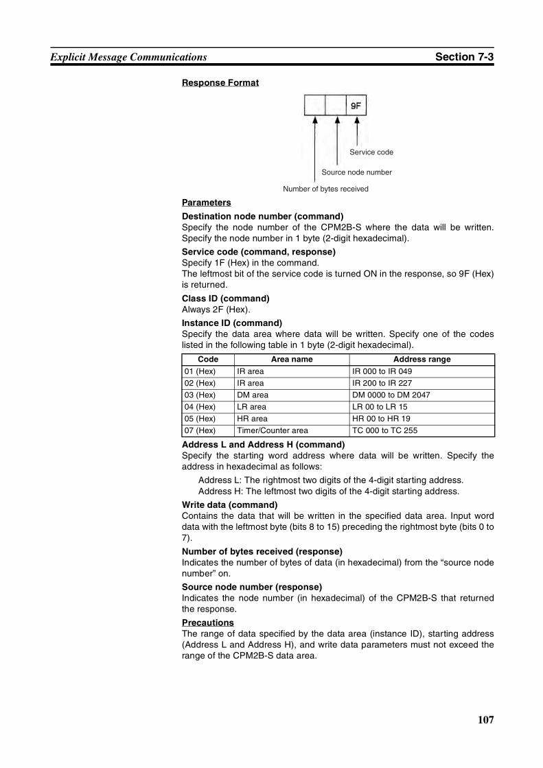
107
Explicit Message Communications Section 7-3
Response Format
Parameters
Destination node number (command)Specify the node number of the CPM2B-S where the data will be written.Specify the node number in 1 byte (2-digit hexadecimal).
Service code (command, response)Specify 1F (Hex) in the command.The leftmost bit of the service code is turned ON in the response, so 9F (Hex)is returned.
Class ID (command)Always 2F (Hex).
Instance ID (command)Specify the data area where data will be written. Specify one of the codeslisted in the following table in 1 byte (2-digit hexadecimal).
Address L and Address H (command)Specify the starting word address where data will be written. Specify theaddress in hexadecimal as follows:
Address L: The rightmost two digits of the 4-digit starting address.Address H: The leftmost two digits of the 4-digit starting address.
Write data (command)Contains the data that will be written in the specified data area. Input worddata with the leftmost byte (bits 8 to 15) preceding the rightmost byte (bits 0 to7).
Number of bytes received (response)Indicates the number of bytes of data (in hexadecimal) from the “source nodenumber” on.
Source node number (response)Indicates the node number (in hexadecimal) of the CPM2B-S that returnedthe response.
PrecautionsThe range of data specified by the data area (instance ID), starting address(Address L and Address H), and write data parameters must not exceed therange of the CPM2B-S data area.
Code Area name Address range01 (Hex) IR area IR 000 to IR 049
02 (Hex) IR area IR 200 to IR 227
03 (Hex) DM area DM 0000 to DM 2047
04 (Hex) LR area LR 00 to LR 15
05 (Hex) HR area HR 00 to HR 19
07 (Hex) Timer/Counter area TC 000 to TC 255
Number of bytes received
Source node number
Service code
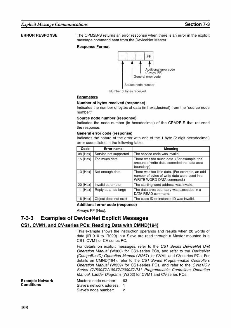
108
Explicit Message Communications Section 7-3
ERROR RESPONSE The CPM2B-S returns an error response when there is an error in the explicitmessage command sent from the DeviceNet Master.
Response Format
Parameters
Number of bytes received (response)Indicates the number of bytes of data (in hexadecimal) from the “source nodenumber.”
Source node number (response)Indicates the node number (in hexadecimal) of the CPM2B-S that returnedthe response.
General error code (response)Indicates the nature of the error with one of the 1-byte (2-digit hexadecimal)error codes listed in the following table.
Additional error code (response)
Always FF (Hex).
7-3-3 Examples of DeviceNet Explicit MessagesCS1, CVM1, and CV-series PCs: Reading Data with CMND(194)
This example shows the instruction operands and results when 20 words ofdata (IR 010 to IR029) in a Slave are read through a Master mounted in aCS1, CVM1 or CV-series PC.
For details on explicit messages, refer to the CS1 Series DeviceNet UnitOperation Manual (W380) for CS1-series PCs, and refer to the DeviceNet(CompoBus/D) Operation Manual (W267) for CVM1 and CV-series PCs. Fordetails on CMND(194), refer to the CS1 Series Programmable ControllersOperation Manual (W339) for CS1-series PCs, and refer to the CVM1/CVSeries CV500/CV100/CV2000/CVM1 Programmable Controllers OperationManual: Ladder Diagrams (W202) for CVM1 and CV-series PCs.
Example Network Conditions
Master’s node number: 63Slave’s network address: 1Slave’s node number: 2
Code Error name Meaning08 (Hex) Service not supported The service code was invalid.
15 (Hex) Too much data There was too much data. (For example, the amount of write data exceeded the data area boundary.)
13 (Hex) Not enough data There was too little data. (For example, an odd number of bytes of write data were used in a WRITE WORD DATA command.)
20 (Hex) Invalid parameter The starting word address was invalid.
11 (Hex) Reply data too large The data area boundary was exceeded in a DATA READ command.
16 (Hex) Object does not exist The class ID or instance ID was invalid.
Number of bytes received
Source node number
General error code
Additional error code(Always FF)
109
Explicit Message Communications Section 7-3
CMND(194) Operand Details
• Command Words
• Response Words(The results are stored as follows.)
• Control Words
CS1, CVM1, and CV-series PCs: Writing Data with CMND(194)This example shows the instruction operands and results when 20 words ofdata are written through a Master mounted in a CS1, CVM1, or CV-series PCto words IR 010 to IR 029 in a Slave.
For details on explicit messages, refer to the CS1 Series DeviceNet UnitOperation Manual (W380) for CS1-series PCs, and refer to the DeviceNet(CompoBus/D) Operation Manual (W267) for CVM1 and CV-series PCs. Fordetails on CMND(194), refer to the CS1 Series Programmable ControllersOperation Manual (W339) for CS1-series PCs, and refer to the CVM1/CVSeries CV500/CV100/CV2000/CVM1 Programmable Controllers OperationManual: Ladder Diagrams (W202) for CVM1 and CV-series PCs.
[CMND S D C]
Word Contents (Hex)
Function
S 28 01 EXPLICIT MESSAGE SEND command code = 2801 (Hex)
S+1 02 1C Slave node number = 02 (Hex)READ BYTE DATA command service code = 1C (Hex)
S+2 00 2F Class ID = 002F (Hex)
S+3 00 01 Instance ID = 0001 (Hex) specifies data area
S+4 0A 00 Starting read address = 000A (Hex) specifies IR 010Address L = 0A (Hex); Address H = 00 (Hex)
S+5 28 00 Number of bytes = 28 (Hex) specifies 40 bytes(The rightmost byte of S+5 is not used.)
Word Contents (Hex)
Function
D 28 01 EXPLICIT MESSAGE SEND command code = 2801 (Hex)
D+1 00 00 Normal completion code = 0000 (Hex)
D+2 00 2A Number of bytes received = 2A (Hex) indicates 42 bytes(This is the number of bytes from D+3 to the end.)
D+3 02 9C Slave’s node number = 02 (Hex)READ BYTE DATA response service code = 9C (Hex)
D+4
to
D+23
HH LL
:
HH LL
These words contain the data read from slave words IR 010 to IR 029. When the READ BYTE DATA command is executed from an OMRON Master, the bytes are stored in the same order (HH LL) in which they were stored in the Slave.
Word Contents (Hex)
Function
C 00 0B Number of bytes of command data beginning with word S = 0B (Hex) specifies 11 bytes
C+1 00 30 Number of bytes of response data beginning with word D = 30 (Hex) specifies 48 bytes
C+2 00 01 Destination network address = 01 (Hex)
C+3 3F FE Master’s node number = 3F (Hex) specifies 63Master’s unit address = FE (Hex) specifies the local Unit
C+4 00 00 Response requiredTransmission port number = 00 (Hex) specifies 0Number of retries = 00 (Hex) specifies 0
C+5 00 64 Response monitoring time = 64 (Hex) specifies 10.0 seconds
110
Explicit Message Communications Section 7-3
Example Network Conditions
Master’s node number: 63Slave’s network address: 1Slave’s node number: 2
CMND(194) Operand Details
• Command Words
• Response Words(The results are stored as follows.)
• Control Words
[CMND S D C]
Word Contents (Hex)
Function
S 28 01 EXPLICIT MESSAGE SEND command code = 2801 (Hex)S+1 02 1C Slave node number = 02 (Hex)
WRITE BYTE DATA command service code = 1E (Hex)S+2 00 2F Class ID = 002F (Hex)S+3 00 01 Instance ID = 0001 (Hex) specifies data areaS+4 0A 00 Starting write address = 000A (Hex) specifies IR 010
Address L = 0A (Hex); Address H = 00 (Hex)S+5
to
S+24
HH LL
:
HH LL
These words contain the data to be written to slave words IR 010 to IR 029. When the WRITE BYTE DATA command is executed from an OMRON Master, the bytes are written to the Slave in the same order (HH LL) in which they appear in the Master.
Word Contents (Hex)
Function
D 28 01 EXPLICIT MESSAGE SEND command code = 2801 (Hex)D+1 00 00 Normal completion code = 0000 (Hex)D+2 00 02 Number of bytes received = 02 (Hex) indicates 2 bytes
(This is the number of bytes from D+3 to the end.)D+3 02 9C Slave’s node number = 02 (Hex)
WRITE BYTE DATA response service code = 9E (Hex)
Word Contents (Hex)
Function
C 00 32 Number of bytes of command data beginning with word S = 32 (Hex) specifies 50 bytes
C+1 00 08 Number of bytes of response data beginning with word D = 08 (Hex) specifies 8 bytes
C+2 00 01 Destination network address = 01 (Hex)C+3 3F FE Master’s node number = 3F (Hex) specifies 63
Master’s unit address = FE (Hex) specifies the local UnitC+4 00 00 Response required
Transmission port number = 00 (Hex) specifies 0Number of retries = 00 (Hex) specifies 0
C+5 00 64 Response monitoring time = 64 (Hex) specifies 10.0 seconds
111
Explicit Message Communications Section 7-3
C200HX/HG/HE PCs: Reading Data with IOWR(– –)This example shows the instruction operands and results when 20 words ofdata (IR 010 to IR029) in a Slave are read through a Master mounted in aC200HX/HG/HE PC and stored in words DM 2000 to DM 2019.
Refer to the DeviceNet (CompoBus/D) Masters Operation Manual for detailson explicit messages and refer to the C200HX/HG/HE Programmable Control-lers Operation Manual for details on IOWR(– –).
Example Network Conditions
The Master’s node number is 63, the Slave’s network address is 0, and theSlave’s node number is 2.
IOWR(– –) Operand Details
• Control Code
• Command Words (Source information)
• Destination Information
• Response Words (The results are stored as follows.)
[IOWR C S D]
Word Contents (Hex)
Function
C 3F FE Master’s node number = 3F (Hex) specifies 63Master’s unit address = FE (Hex) specifies the local Unit
Word Contents (Hex)
Function
S 82 07 Specifies starting response word = DM 200082 (Hex) specifies the DM area07D0 (Hex) specifies address 2000(Refer to the C200HX/HG/HE Operation Manual for details.)
S+1 D0 00
S+2 00 64 Response monitoring time = 64 (Hex) specifies 10.0 secondsS+3 00 0B Number of bytes of command data beginning with word S+4 =
0B (Hex) specifies 11 bytesS+4 28 01 EXPLICIT MESSAGE SEND command code = 2801 (Hex)S+5 02 1C Slave node number = 02 (Hex)
READ BYTE DATA command service code = 1C (Hex)S+6 00 2F Class ID = 002F (Hex)S+7 00 01 Instance ID = 0001 (Hex) specifies data areaS+8 0A 00 Starting read address = 000A (Hex) specifies IR 010
Address L = 0A (Hex); Address H = 00 (Hex)S+9 28 00 Number of bytes = 28 (Hex) specifies 40 bytes
(The rightmost byte of S+5 is not used.)
Word Contents (Hex)
Function
D 00 10 Master Unit’s unit number = 00Number of words of command data beginning with word S = 10 (BCD) specifies 10 words
Word Contents (Hex)
Function
DM 2000 28 01 EXPLICIT MESSAGE SEND command code = 2801 (Hex)DM 2001 00 00 Normal completion code = 0000 (Hex)DM 2002 00 2A Number of bytes received = 2A (Hex) indicates 42 bytes
(This is the number of bytes from D+3 to the end.)DM 2003 02 9C Slave’s node number = 02 (Hex)
READ BYTE DATA response service code = 9C (Hex)DM 2004
to
DM 2023
HH LL
:
HH LL
These words contain the data read from slave words IR 010 to IR 029. When the READ BYTE DATA command is exe-cuted from an OMRON Master, the bytes are stored in the same order (HH LL) in which they were stored in the Slave.
112
Explicit Message Communications Section 7-3
C200HX/HG/HE PCs: Writing Data with IOWR(– –)This example shows the instruction operands and results when 20 words ofdata are written from a Master mounted in a C200HX/HG/HE PC to words IR010 to IR029 in a Slave.
Refer to the DeviceNet (CompoBus/D) Masters Operation Manual for detailson explicit messages and refer to the C200HX/HG/HE Programmable Control-lers Operation Manual for details on IOWR(– –).
Example Network Conditions
Master’s node number: 63Slave’s network address: 0Slave’s node number: 2
IOWR(– –) Operand Details
• Control Code
• Command Words (Source Information)
• Destination Information
• Response Words (The results are stored as follows.)
[IOWR C S D]
Word Contents (Hex)
Function
C 3F FE Master’s node number = 3F (Hex) specifies 63Master’s unit address = FE (Hex) specifies the local Unit
Word Contents (Hex)
Function
S 82 07 Specifies starting response word = DM 2000
82 (Hex) specifies the DM area07D0 (Hex) specifies address 2000(Refer to the C200HX/HG/HE Operation Manual for details.)
S+1 D0 00
S+2 00 64 Response monitoring time = 64 (Hex) specifies 10.0 seconds
S+3 00 0B Number of bytes of command data beginning with word S+4 = 32 (Hex) specifies 50 bytes
S+4 28 01 EXPLICIT MESSAGE SEND command code = 2801 (Hex)
S+5 02 1E Slave node number = 02 (Hex)WRITE BYTE DATA command service code = 1E (Hex)
S+6 00 2F Class ID = 002F (Hex)
S+7 00 01 Instance ID = 0001 (Hex) specifies data area
S+8 0A 00 Starting write address = 000A (Hex) specifies IR 010Address L = 0A (Hex); Address H = 00 (Hex)
S+9
to
S+28
HH LL
:
HH LL
These words contain the data to be written to slave words IR 010 to IR 029. When the WRITE BYTE DATA command is executed from an OMRON Master, the bytes are written to the Slave in the same order (HH LL) in which they appear in the Master.
Word Contents (Hex)
Function
D 00 29 Master Unit’s unit number = 00Number of words of command data beginning with word S = 29 (BCD) specifies 29 words
Word Contents (Hex)
Function
DM 2000 28 01 EXPLICIT MESSAGE SEND command code = 2801 (Hex)
DM 2001 00 00 Normal completion code = 0000 (Hex)
DM 2002 00 02 Number of bytes received = 02 (Hex) indicates 2 bytes(This is the number of bytes from D+3 to the end.)
DM 2003 02 9E Slave’s node number = 02 (Hex)READ BYTE DATA response service code = 9E (Hex)
113
Status Information Section 7-4
7-4 Status InformationThe status of DeviceNet communications is indicated by the CPM2B-S PC’sLED indicators and AR area flags. In addition, the PC Setup can be set so thatthe CPM2B-S PC’s operating status information is attached to remote I/Otransmissions from the CPM2B-S to the Master Unit.
7-4-1 LED IndicatorsThe status of DeviceNet communications is indicated on the CPM2B-S PC’sLED indicators.
MS NS
Indicator Color Status Function MeaningMS Green Lit Normal status Normal status
Flashing Incomplete settings status Reading switch settings
Red Lit Fatal error Hardware error (watchdog timer error)
Flashing Non-fatal error Error such as incorrect switch settings
--- Not lit Power is not being supplied. • Power is not being supplied.• Waiting for initialization to start• Reset in progress
NS Green Lit Online/Communications established Normal network status when communica-tions have been established
Flashing Online/Communications not established Normal network status when communica-tions haven’t been established
Red Lit Fatal communications error Communications error (The Unit detected an error indicating that network communica-tions are disabled.)
• Node number duplication• Bus off error detected
Flashing Non-fatal communications error Communications timeout
--- Not lit Offline/Power supply OFF Waiting for completion of the node number duplication check in the Master.
• Incorrect switch settings• Power supply OFF
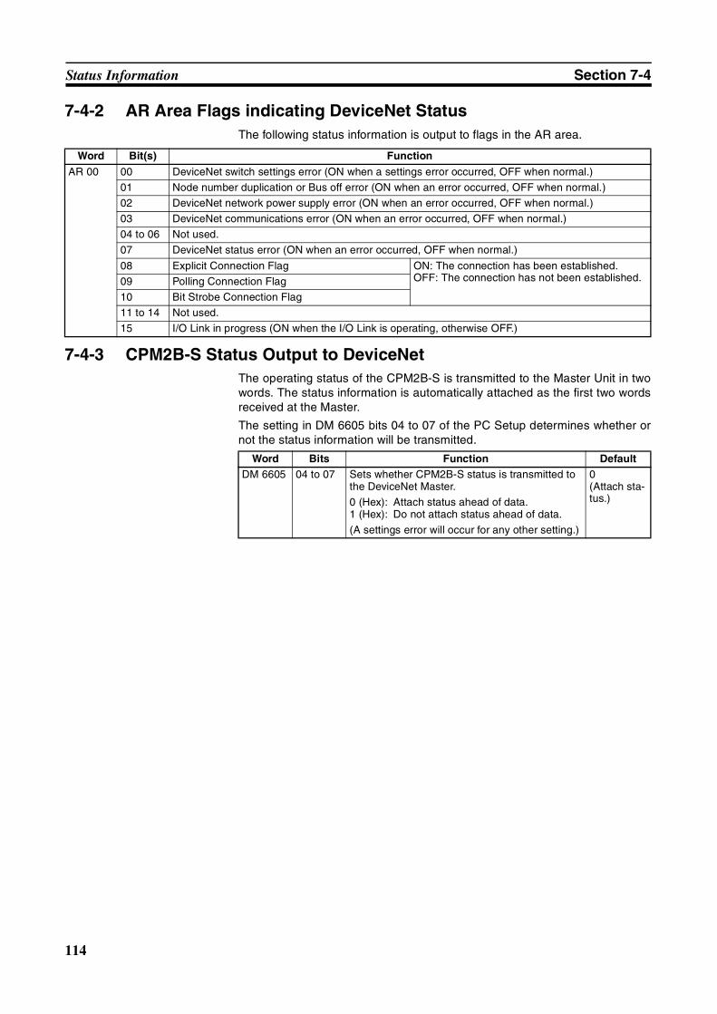
114
Status Information Section 7-4
7-4-2 AR Area Flags indicating DeviceNet StatusThe following status information is output to flags in the AR area.
7-4-3 CPM2B-S Status Output to DeviceNetThe operating status of the CPM2B-S is transmitted to the Master Unit in twowords. The status information is automatically attached as the first two wordsreceived at the Master.
The setting in DM 6605 bits 04 to 07 of the PC Setup determines whether ornot the status information will be transmitted.
Word Bit(s) FunctionAR 00 00 DeviceNet switch settings error (ON when a settings error occurred, OFF when normal.)
01 Node number duplication or Bus off error (ON when an error occurred, OFF when normal.)
02 DeviceNet network power supply error (ON when an error occurred, OFF when normal.)
03 DeviceNet communications error (ON when an error occurred, OFF when normal.)
04 to 06 Not used.
07 DeviceNet status error (ON when an error occurred, OFF when normal.)
08 Explicit Connection Flag ON: The connection has been established.OFF: The connection has not been established.09 Polling Connection Flag
10 Bit Strobe Connection Flag
11 to 14 Not used.
15 I/O Link in progress (ON when the I/O Link is operating, otherwise OFF.)
Word Bits Function DefaultDM 6605 04 to 07 Sets whether CPM2B-S status is transmitted to
the DeviceNet Master.
0 (Hex): Attach status ahead of data.1 (Hex): Do not attach status ahead of data.
(A settings error will occur for any other setting.)
0(Attach sta-tus.)
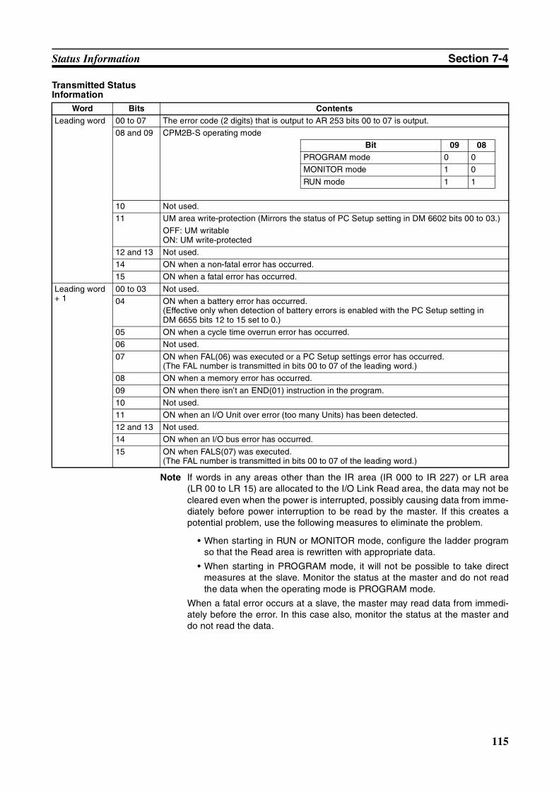
115
Status Information Section 7-4
Transmitted Status Information
Note If words in any areas other than the IR area (IR 000 to IR 227) or LR area(LR 00 to LR 15) are allocated to the I/O Link Read area, the data may not becleared even when the power is interrupted, possibly causing data from imme-diately before power interruption to be read by the master. If this creates apotential problem, use the following measures to eliminate the problem.
• When starting in RUN or MONITOR mode, configure the ladder programso that the Read area is rewritten with appropriate data.
• When starting in PROGRAM mode, it will not be possible to take directmeasures at the slave. Monitor the status at the master and do not readthe data when the operating mode is PROGRAM mode.
When a fatal error occurs at a slave, the master may read data from immedi-ately before the error. In this case also, monitor the status at the master anddo not read the data.
Word Bits ContentsLeading word 00 to 07 The error code (2 digits) that is output to AR 253 bits 00 to 07 is output.
08 and 09 CPM2B-S operating mode
Bit 09 08PROGRAM mode 0 0
MONITOR mode 1 0
RUN mode 1 1
10 Not used.
11 UM area write-protection (Mirrors the status of PC Setup setting in DM 6602 bits 00 to 03.)
OFF: UM writableON: UM write-protected
12 and 13 Not used.
14 ON when a non-fatal error has occurred.
15 ON when a fatal error has occurred.
Leading word + 1
00 to 03 Not used.
04 ON when a battery error has occurred.(Effective only when detection of battery errors is enabled with the PC Setup setting in DM 6655 bits 12 to 15 set to 0.)
05 ON when a cycle time overrun error has occurred.
06 Not used.
07 ON when FAL(06) was executed or a PC Setup settings error has occurred.(The FAL number is transmitted in bits 00 to 07 of the leading word.)
08 ON when a memory error has occurred.
09 ON when there isn’t an END(01) instruction in the program.
10 Not used.
11 ON when an I/O Unit over error (too many Units) has been detected.
12 and 13 Not used.
14 ON when an I/O bus error has occurred.
15 ON when FALS(07) was executed.(The FAL number is transmitted in bits 00 to 07 of the leading word.)
117
SECTION 8Cycle Time and I/O Response Time
This section explains the cycle time and I/O response time in CPM2B-S PCs. Refer to this section when writing the userprogram to improve operation and reduce response delays.
8-1 Cycle Time . . . . . . . . . . . . . . . . . . . . . . . . . . . . . . . . . . . . . . . . . . . . . . . . . . . 118
8-1-1 Cyclic Operation and Interrupts . . . . . . . . . . . . . . . . . . . . . . . . . . . . 118
8-1-2 Cycle Time and Operations . . . . . . . . . . . . . . . . . . . . . . . . . . . . . . . 120
8-1-3 Cycle Time Example . . . . . . . . . . . . . . . . . . . . . . . . . . . . . . . . . . . . 120
8-1-4 Instruction Execution Times . . . . . . . . . . . . . . . . . . . . . . . . . . . . . . . 121
8-2 I/O Response Time . . . . . . . . . . . . . . . . . . . . . . . . . . . . . . . . . . . . . . . . . . . . . 131
8-2-1 CPM2B-S I/O Response Time . . . . . . . . . . . . . . . . . . . . . . . . . . . . . 131
8-2-2 I/O Response Time between CompoBus/S Slaves . . . . . . . . . . . . . . 132
8-3 Interrupt Processing Time . . . . . . . . . . . . . . . . . . . . . . . . . . . . . . . . . . . . . . . . 133
8-4 One-to-one PC Link I/O Response Time . . . . . . . . . . . . . . . . . . . . . . . . . . . . 134
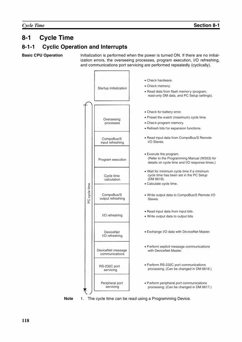
118
Cycle Time Section 8-1
8-1 Cycle Time8-1-1 Cyclic Operation and InterruptsBasic CPU Operation Initialization is performed when the power is turned ON. If there are no initial-
ization errors, the overseeing processes, program execution, I/O refreshing,and communications port servicing are performed repeatedly (cyclically).
Note 1. The cycle time can be read using a Programming Device.
Startup initialization
Overseeing processes
Program execution
Cycle time calculation
I/O refreshing
RS-232C port servicing
• Check hardware.
• Check memory.
• Read data from flash memory (program, read-only DM data, and PC Setup settings).
• Check for battery error.
• Preset the watch (maximum) cycle time.
• Check program memory.
• Refresh bits for expansion functions.
• Execute the program.(Refer to the Programming Manual (W353) for details on cycle time and I/O response times.)
• Wait for minimum cycle time if a minimum cycle time has been set in the PC Setup (DM 6619).
• Calculate cycle time.
• Read input data from input bits .
• Write output data to output bits.
• Perform RS-232C port communications processing. (Can be changed in DM 6616.)
• Perform peripheral port communications processing. (Can be changed in DM 6617.)
• Read input data from CompoBus/S Remote I/O Slaves.
• Write output data to CompoBus/S Remote I/O Slaves.
• Exchange I/O data with DeviceNet Master.
CompoBus/S input refreshing
CompoBus/S output refreshing
DeviceNet I/O refreshing
• Perform explicit message communications with DeviceNet Master.DeviceNet message
communications
Peripheral port servicing
PC
cyc
le ti
me
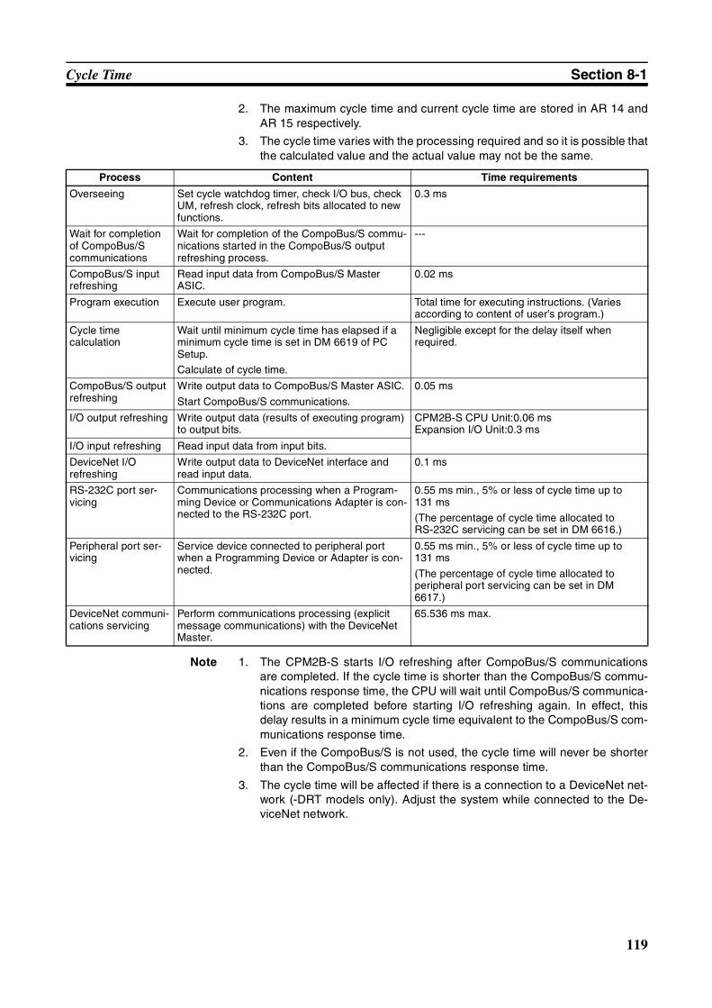
119
Cycle Time Section 8-1
2. The maximum cycle time and current cycle time are stored in AR 14 andAR 15 respectively.
3. The cycle time varies with the processing required and so it is possible thatthe calculated value and the actual value may not be the same.
Note 1. The CPM2B-S starts I/O refreshing after CompoBus/S communicationsare completed. If the cycle time is shorter than the CompoBus/S commu-nications response time, the CPU will wait until CompoBus/S communica-tions are completed before starting I/O refreshing again. In effect, thisdelay results in a minimum cycle time equivalent to the CompoBus/S com-munications response time.
2. Even if the CompoBus/S is not used, the cycle time will never be shorterthan the CompoBus/S communications response time.
3. The cycle time will be affected if there is a connection to a DeviceNet net-work (-DRT models only). Adjust the system while connected to the De-viceNet network.
Process Content Time requirements
Overseeing Set cycle watchdog timer, check I/O bus, check UM, refresh clock, refresh bits allocated to new functions.
0.3 ms
Wait for completion of CompoBus/S communications
Wait for completion of the CompoBus/S commu-nications started in the CompoBus/S output refreshing process.
---
CompoBus/S input refreshing
Read input data from CompoBus/S Master ASIC.
0.02 ms
Program execution Execute user program. Total time for executing instructions. (Varies according to content of user’s program.)
Cycle timecalculation
Wait until minimum cycle time has elapsed if a minimum cycle time is set in DM 6619 of PC Setup.
Calculate of cycle time.
Negligible except for the delay itself when required.
CompoBus/S output refreshing
Write output data to CompoBus/S Master ASIC.
Start CompoBus/S communications.
0.05 ms
I/O output refreshing Write output data (results of executing program) to output bits.
CPM2B-S CPU Unit:0.06 msExpansion I/O Unit:0.3 ms
I/O input refreshing Read input data from input bits.
DeviceNet I/O refreshing
Write output data to DeviceNet interface and read input data.
0.1 ms
RS-232C port ser-vicing
Communications processing when a Program-ming Device or Communications Adapter is con-nected to the RS-232C port.
0.55 ms min., 5% or less of cycle time up to 131 ms
(The percentage of cycle time allocated to RS-232C servicing can be set in DM 6616.)
Peripheral port ser-vicing
Service device connected to peripheral port when a Programming Device or Adapter is con-nected.
0.55 ms min., 5% or less of cycle time up to 131 ms
(The percentage of cycle time allocated to peripheral port servicing can be set in DM 6617.)
DeviceNet communi-cations servicing
Perform communications processing (explicit message communications) with the DeviceNet Master.
65.536 ms max.
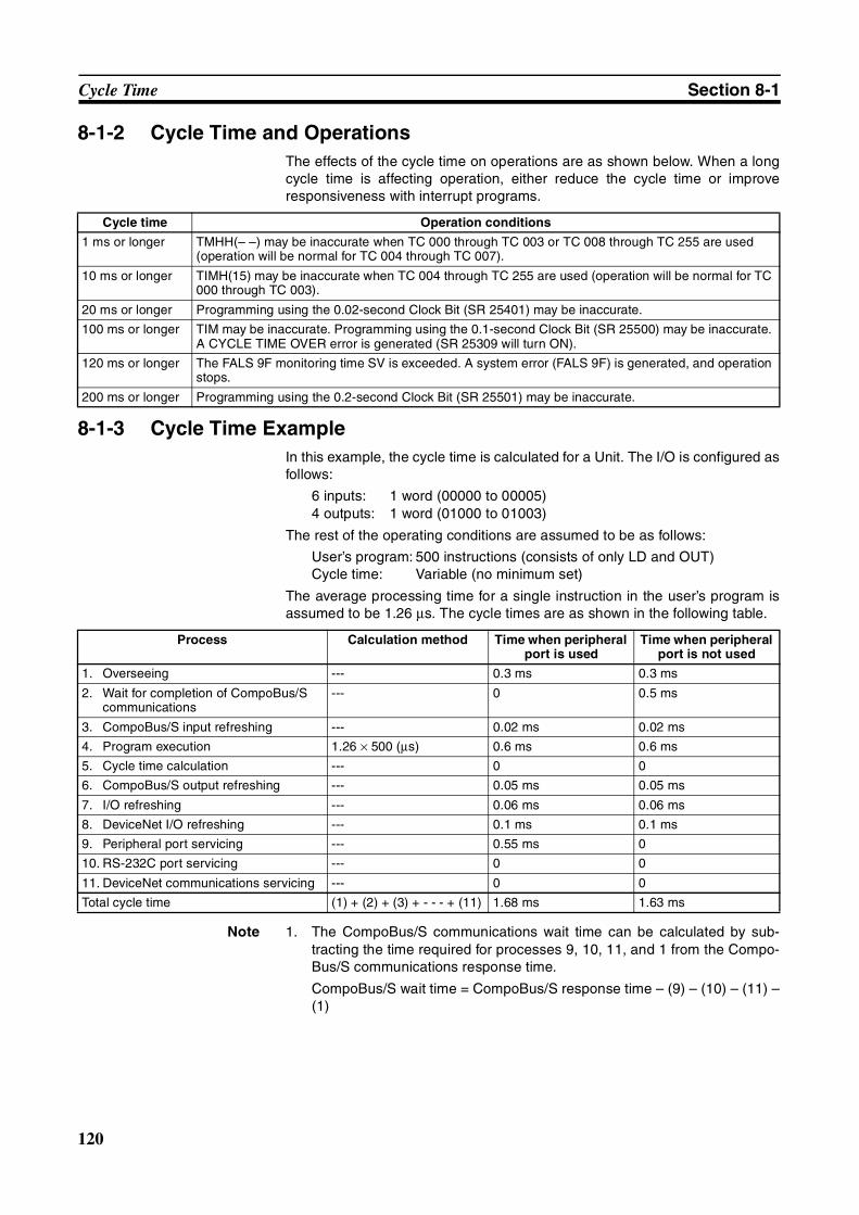
120
Cycle Time Section 8-1
8-1-2 Cycle Time and OperationsThe effects of the cycle time on operations are as shown below. When a longcycle time is affecting operation, either reduce the cycle time or improveresponsiveness with interrupt programs.
8-1-3 Cycle Time ExampleIn this example, the cycle time is calculated for a Unit. The I/O is configured asfollows:
6 inputs: 1 word (00000 to 00005)4 outputs: 1 word (01000 to 01003)
The rest of the operating conditions are assumed to be as follows:
User’s program: 500 instructions (consists of only LD and OUT)Cycle time: Variable (no minimum set)
The average processing time for a single instruction in the user’s program isassumed to be 1.26 µs. The cycle times are as shown in the following table.
Note 1. The CompoBus/S communications wait time can be calculated by sub-tracting the time required for processes 9, 10, 11, and 1 from the Compo-Bus/S communications response time.
CompoBus/S wait time = CompoBus/S response time – (9) – (10) – (11) –(1)
Cycle time Operation conditions
1 ms or longer TMHH(– –) may be inaccurate when TC 000 through TC 003 or TC 008 through TC 255 are used (operation will be normal for TC 004 through TC 007).
10 ms or longer TIMH(15) may be inaccurate when TC 004 through TC 255 are used (operation will be normal for TC 000 through TC 003).
20 ms or longer Programming using the 0.02-second Clock Bit (SR 25401) may be inaccurate.
100 ms or longer TIM may be inaccurate. Programming using the 0.1-second Clock Bit (SR 25500) may be inaccurate. A CYCLE TIME OVER error is generated (SR 25309 will turn ON).
120 ms or longer The FALS 9F monitoring time SV is exceeded. A system error (FALS 9F) is generated, and operation stops.
200 ms or longer Programming using the 0.2-second Clock Bit (SR 25501) may be inaccurate.
Process Calculation method Time when peripheral port is used
Time when peripheral port is not used
1. Overseeing --- 0.3 ms 0.3 ms
2. Wait for completion of CompoBus/S communications
--- 0 0.5 ms
3. CompoBus/S input refreshing --- 0.02 ms 0.02 ms
4. Program execution 1.26 × 500 (µs) 0.6 ms 0.6 ms
5. Cycle time calculation --- 0 0
6. CompoBus/S output refreshing --- 0.05 ms 0.05 ms
7. I/O refreshing --- 0.06 ms 0.06 ms
8. DeviceNet I/O refreshing --- 0.1 ms 0.1 ms
9. Peripheral port servicing --- 0.55 ms 0
10. RS-232C port servicing --- 0 0
11. DeviceNet communications servicing --- 0 0
Total cycle time (1) + (2) + (3) + - - - + (11) 1.68 ms 1.63 ms
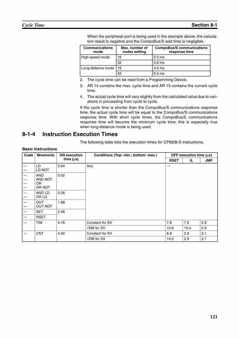
121
Cycle Time Section 8-1
When the peripheral port is being used in the example above, the calcula-tion result is negative and the CompoBus/S wait time is negligible.
2. The cycle time can be read from a Programming Device.
3. AR 14 contains the max. cycle time and AR 15 contains the current cycletime.
4. The actual cycle time will vary slightly from the calculated value due to vari-ations in processing from cycle to cycle.
If the cycle time is shorter than the CompoBus/S communications responsetime, the actual cycle time will be equal to the CompoBus/S communicationsresponse time. With short cycle times, the CompoBus/S communicationsresponse time will become the minimum cycle time; this is especially truewhen long-distance mode is being used.
8-1-4 Instruction Execution TimesThe following table lists the execution times for CPM2B-S instructions.
Basic Instructions
Communications mode
Max. number of nodes setting
CompoBus/S communications response time
High-speed mode 16 0.5 ms
32 0.8 ms
Long-distance mode 16 4.0 ms
32 6.0 ms
Code Mnemonic ON execution time (µs)
Conditions (Top: min.; bottom: max.) OFF execution time (µs)
RSET IL JMP
------
LDLD NOT
0.64 Any ---
------------
ANDAND NOTOROR NOT
0.52
------
AND LDOR LD
0.26
------
OUTOUT NOT
1.88
--- SET 2.58
--- RSET
--- TIM 4.76 Constant for SV 7.8 7.6 2.9
*DM for SV 15.6 15.4 2.9
--- CNT 4.50 Constant for SV 6.8 2.9 3.1
*DM for SV 14.5 2.9 3.1
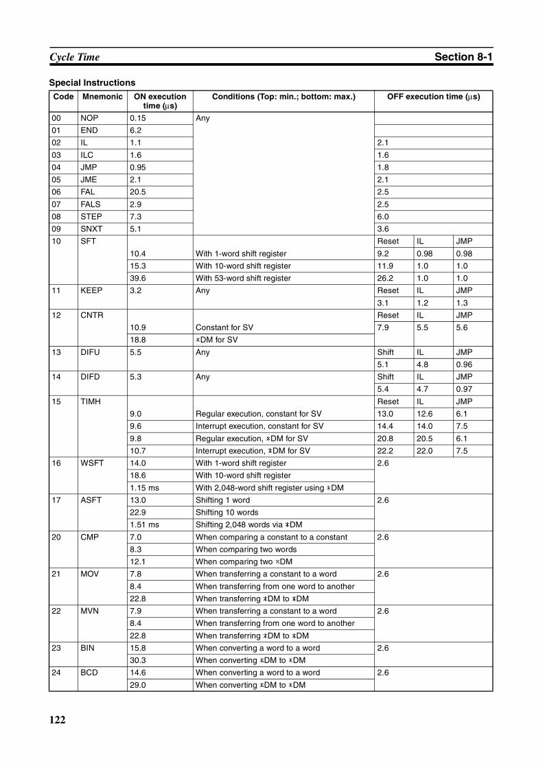
122
Cycle Time Section 8-1
Special Instructions
Code Mnemonic ON execution time (µs)
Conditions (Top: min.; bottom: max.) OFF execution time (µs)
00 NOP 0.15 Any
01 END 6.2
02 IL 1.1 2.1
03 ILC 1.6 1.6
04 JMP 0.95 1.8
05 JME 2.1 2.1
06 FAL 20.5 2.5
07 FALS 2.9 2.5
08 STEP 7.3 6.0
09 SNXT 5.1 3.6
10 SFT Reset IL JMP
10.4 With 1-word shift register 9.2 0.98 0.98
15.3 With 10-word shift register 11.9 1.0 1.0
39.6 With 53-word shift register 26.2 1.0 1.0
11 KEEP 3.2 Any Reset IL JMP
3.1 1.2 1.3
12 CNTR Reset IL JMP
10.9 Constant for SV 7.9 5.5 5.6
18.8 *DM for SV
13 DIFU 5.5 Any Shift IL JMP
5.1 4.8 0.96
14 DIFD 5.3 Any Shift IL JMP
5.4 4.7 0.97
15 TIMH Reset IL JMP
9.0 Regular execution, constant for SV 13.0 12.6 6.1
9.6 Interrupt execution, constant for SV 14.4 14.0 7.5
9.8 Regular execution, *DM for SV 20.8 20.5 6.1
10.7 Interrupt execution, *DM for SV 22.2 22.0 7.5
16 WSFT 14.0 With 1-word shift register 2.6
18.6 With 10-word shift register
1.15 ms With 2,048-word shift register using *DM
17 ASFT 13.0 Shifting 1 word 2.6
22.9 Shifting 10 words
1.51 ms Shifting 2,048 words via *DM
20 CMP 7.0 When comparing a constant to a constant 2.6
8.3 When comparing two words
12.1 When comparing two *DM
21 MOV 7.8 When transferring a constant to a word 2.6
8.4 When transferring from one word to another
22.8 When transferring *DM to *DM
22 MVN 7.9 When transferring a constant to a word 2.6
8.4 When transferring from one word to another
22.8 When transferring *DM to *DM
23 BIN 15.8 When converting a word to a word 2.6
30.3 When converting *DM to *DM
24 BCD 14.6 When converting a word to a word 2.6
29.0 When converting *DM to *DM
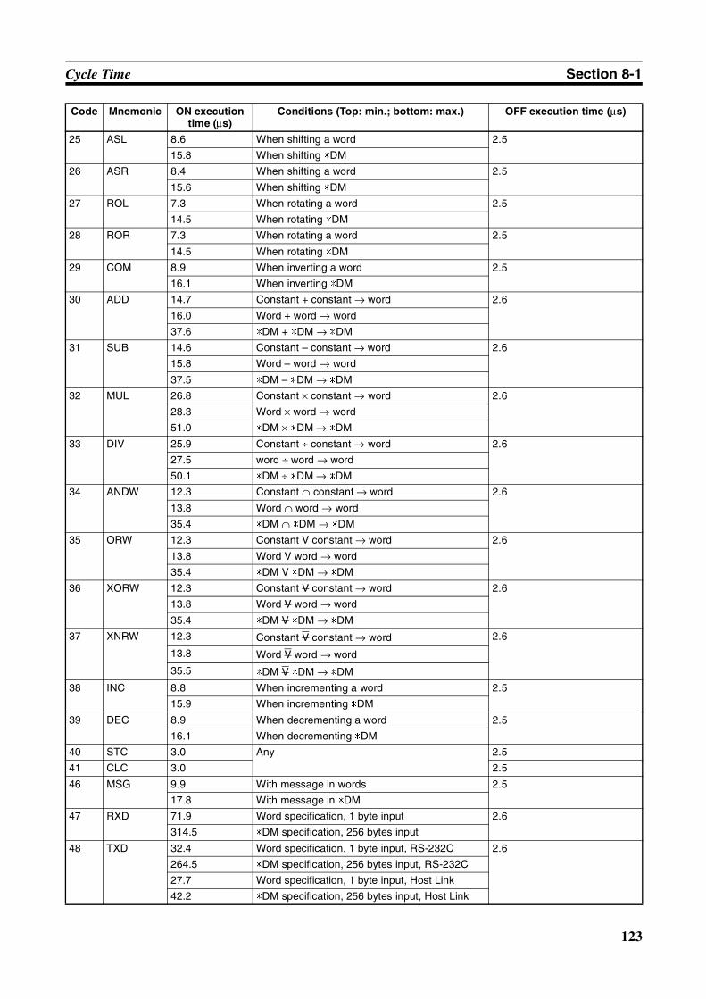
123
Cycle Time Section 8-1
25 ASL 8.6 When shifting a word 2.5
15.8 When shifting *DM
26 ASR 8.4 When shifting a word 2.5
15.6 When shifting *DM
27 ROL 7.3 When rotating a word 2.5
14.5 When rotating *DM
28 ROR 7.3 When rotating a word 2.5
14.5 When rotating *DM
29 COM 8.9 When inverting a word 2.5
16.1 When inverting *DM
30 ADD 14.7 Constant + constant → word 2.6
16.0 Word + word → word
37.6 *DM + *DM → *DM
31 SUB 14.6 Constant – constant → word 2.6
15.8 Word – word → word
37.5 *DM – *DM → *DM
32 MUL 26.8 Constant × constant → word 2.6
28.3 Word × word → word
51.0 *DM × *DM → *DM
33 DIV 25.9 Constant ÷ constant → word 2.6
27.5 word ÷ word → word
50.1 *DM ÷ *DM → *DM
34 ANDW 12.3 Constant ∩ constant → word 2.6
13.8 Word ∩ word → word
35.4 *DM ∩ *DM → *DM
35 ORW 12.3 Constant V constant → word 2.6
13.8 Word V word → word
35.4 *DM V *DM → *DM
36 XORW 12.3 Constant V constant → word 2.6
13.8 Word V word → word
35.4 *DM V *DM → *DM
37 XNRW 12.3 Constant V constant → word 2.6
13.8 Word V word → word
35.5 *DM V *DM → *DM
38 INC 8.8 When incrementing a word 2.5
15.9 When incrementing *DM
39 DEC 8.9 When decrementing a word 2.5
16.1 When decrementing *DM
40 STC 3.0 Any 2.5
41 CLC 3.0 2.5
46 MSG 9.9 With message in words 2.5
17.8 With message in *DM
47 RXD 71.9 Word specification, 1 byte input 2.6
314.5 *DM specification, 256 bytes input
48 TXD 32.4 Word specification, 1 byte input, RS-232C 2.6
264.5 *DM specification, 256 bytes input, RS-232C
27.7 Word specification, 1 byte input, Host Link
42.2 *DM specification, 256 bytes input, Host Link
Code Mnemonic ON execution time (µs)
Conditions (Top: min.; bottom: max.) OFF execution time (µs)
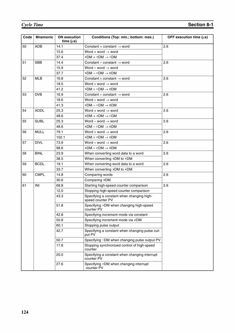
124
Cycle Time Section 8-1
50 ADB 14.1 Constant + constant → word 2.6
15.6 Word + word → word
37.4 *DM + *DM → *DM
51 SBB 14.4 Constant – constant → word 2.6
15.9 Word – word → word
37.7 *DM – *DM → *DM
52 MLB 16.8 Constant × constant → word 2.6
18.5 Word × word → word
41.2 *DM × *DM → *DM
53 DVB 16.9 Constant ÷ constant → word 2.6
18.6 Word ÷ word → word
41.3 *DM ÷ *DM → *DM
54 ADDL 25.3 Word + word → word 2.6
48.6 *DM + *DM → *DM
55 SUBL 25.3 Word – word → word 2.6
48.6 *DM – *DM → *DM
56 MULL 79.1 Word × word → word 2.6
102.1 *DM × *DM → *DM
57 DIVL 73.9 Word ÷ word → word 2.6
98.6 *DM ÷ *DM → *DM
58 BINL 23.9 When converting word data to a word 2.6
38.5 When converting *DM to *DM
59 BCDL 19.1 When converting word data to a word 2.6
33.7 When converting *DM to *DM
60 CMPL 14.8 Comparing words 2.6
30.6 Comparing *DM
61 INI 68.8 Starting high-speed counter comparison 2.6
12.0 Stopping high-speed counter comparison
43.3 Specifying a constant when changing high-speed counter PV
51.8 Specifying *DM when changing high-speed counter PV
42.8 Specifying increment mode via constant
50.8 Specifying increment mode via *DM
60.1 Stopping pulse output
42.7 Specifying a constant when changing pulse out-put PV
50.7 Specifying *DM when changing pulse output PV
17.8 Stopping synchronized control of high-speed counter
20.0 Specifying a constant when changing interrupt counter PV
27.6 Specifying *DM when changing interrupt counter PV
Code Mnemonic ON execution time (µs)
Conditions (Top: min.; bottom: max.) OFF execution time (µs)
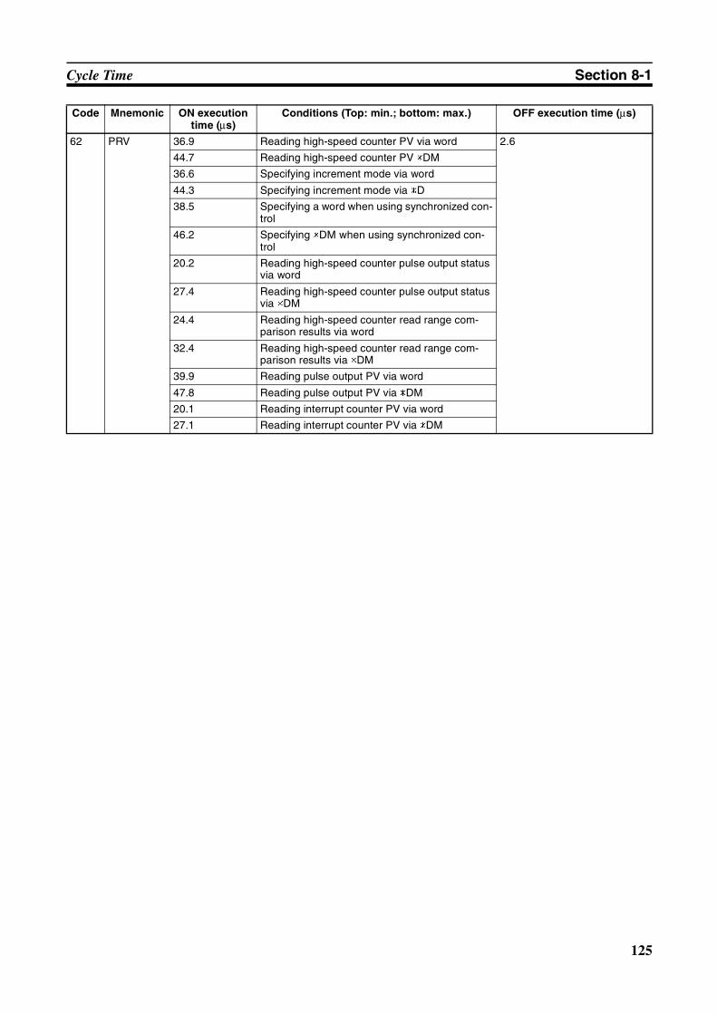
125
Cycle Time Section 8-1
62 PRV 36.9 Reading high-speed counter PV via word 2.6
44.7 Reading high-speed counter PV *DM
36.6 Specifying increment mode via word
44.3 Specifying increment mode via *D
38.5 Specifying a word when using synchronized con-trol
46.2 Specifying *DM when using synchronized con-trol
20.2 Reading high-speed counter pulse output status via word
27.4 Reading high-speed counter pulse output status via *DM
24.4 Reading high-speed counter read range com-parison results via word
32.4 Reading high-speed counter read range com-parison results via *DM
39.9 Reading pulse output PV via word
47.8 Reading pulse output PV via *DM
20.1 Reading interrupt counter PV via word
27.1 Reading interrupt counter PV via *DM
Code Mnemonic ON execution time (µs)
Conditions (Top: min.; bottom: max.) OFF execution time (µs)
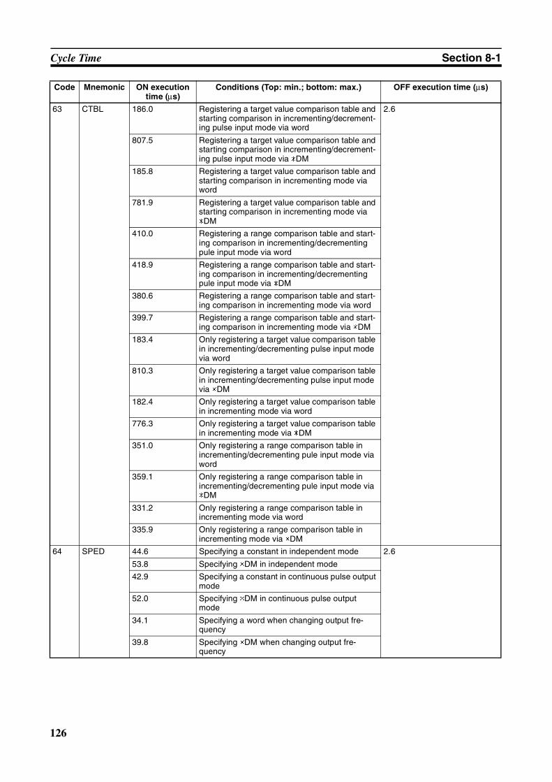
126
Cycle Time Section 8-1
63 CTBL 186.0 Registering a target value comparison table and starting comparison in incrementing/decrement-ing pulse input mode via word
2.6
807.5 Registering a target value comparison table and starting comparison in incrementing/decrement-ing pulse input mode via *DM
185.8 Registering a target value comparison table and starting comparison in incrementing mode via word
781.9 Registering a target value comparison table and starting comparison in incrementing mode via *DM
410.0 Registering a range comparison table and start-ing comparison in incrementing/decrementing pule input mode via word
418.9 Registering a range comparison table and start-ing comparison in incrementing/decrementing pule input mode via *DM
380.6 Registering a range comparison table and start-ing comparison in incrementing mode via word
399.7 Registering a range comparison table and start-ing comparison in incrementing mode via *DM
183.4 Only registering a target value comparison table in incrementing/decrementing pulse input mode via word
810.3 Only registering a target value comparison table in incrementing/decrementing pulse input mode via *DM
182.4 Only registering a target value comparison table in incrementing mode via word
776.3 Only registering a target value comparison table in incrementing mode via *DM
351.0 Only registering a range comparison table in incrementing/decrementing pule input mode via word
359.1 Only registering a range comparison table in incrementing/decrementing pule input mode via *DM
331.2 Only registering a range comparison table in incrementing mode via word
335.9 Only registering a range comparison table in incrementing mode via *DM
64 SPED 44.6 Specifying a constant in independent mode 2.6
53.8 Specifying *DM in independent mode
42.9 Specifying a constant in continuous pulse output mode
52.0 Specifying *DM in continuous pulse output mode
34.1 Specifying a word when changing output fre-quency
39.8 Specifying *DM when changing output fre-quency
Code Mnemonic ON execution time (µs)
Conditions (Top: min.; bottom: max.) OFF execution time (µs)
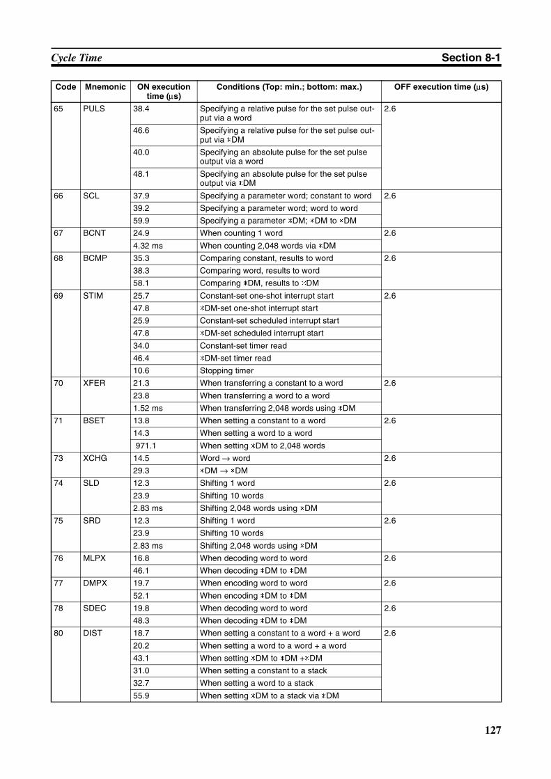
127
Cycle Time Section 8-1
65 PULS 38.4 Specifying a relative pulse for the set pulse out-put via a word
2.6
46.6 Specifying a relative pulse for the set pulse out-put via *DM
40.0 Specifying an absolute pulse for the set pulse output via a word
48.1 Specifying an absolute pulse for the set pulse output via *DM
66 SCL 37.9 Specifying a parameter word; constant to word 2.6
39.2 Specifying a parameter word; word to word
59.9 Specifying a parameter *DM; *DM to *DM
67 BCNT 24.9 When counting 1 word 2.6
4.32 ms When counting 2,048 words via *DM
68 BCMP 35.3 Comparing constant, results to word 2.6
38.3 Comparing word, results to word
58.1 Comparing *DM, results to *DM
69 STIM 25.7 Constant-set one-shot interrupt start 2.6
47.8 *DM-set one-shot interrupt start
25.9 Constant-set scheduled interrupt start
47.8 *DM-set scheduled interrupt start
34.0 Constant-set timer read
46.4 *DM-set timer read
10.6 Stopping timer
70 XFER 21.3 When transferring a constant to a word 2.6
23.8 When transferring a word to a word
1.52 ms When transferring 2,048 words using *DM
71 BSET 13.8 When setting a constant to a word 2.6
14.3 When setting a word to a word
971.1 When setting *DM to 2,048 words
73 XCHG 14.5 Word → word 2.6
29.3 *DM → *DM
74 SLD 12.3 Shifting 1 word 2.6
23.9 Shifting 10 words
2.83 ms Shifting 2,048 words using *DM
75 SRD 12.3 Shifting 1 word 2.6
23.9 Shifting 10 words
2.83 ms Shifting 2,048 words using *DM
76 MLPX 16.8 When decoding word to word 2.6
46.1 When decoding *DM to *DM
77 DMPX 19.7 When encoding word to word 2.6
52.1 When encoding *DM to *DM
78 SDEC 19.8 When decoding word to word 2.6
48.3 When decoding *DM to *DM
80 DIST 18.7 When setting a constant to a word + a word 2.6
20.2 When setting a word to a word + a word
43.1 When setting *DM to *DM +*DM
31.0 When setting a constant to a stack
32.7 When setting a word to a stack
55.9 When setting *DM to a stack via *DM
Code Mnemonic ON execution time (µs)
Conditions (Top: min.; bottom: max.) OFF execution time (µs)
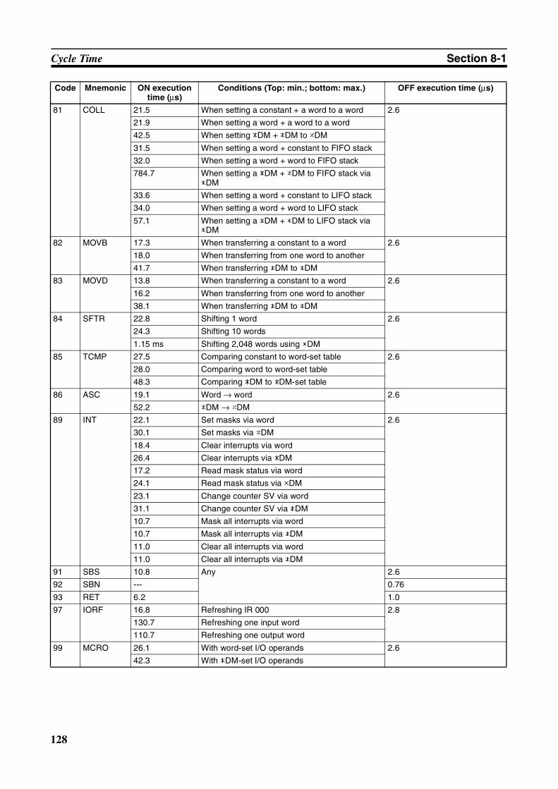
128
Cycle Time Section 8-1
81 COLL 21.5 When setting a constant + a word to a word 2.6
21.9 When setting a word + a word to a word
42.5 When setting *DM + *DM to *DM
31.5 When setting a word + constant to FIFO stack
32.0 When setting a word + word to FIFO stack
784.7 When setting a *DM + *DM to FIFO stack via *DM
33.6 When setting a word + constant to LIFO stack
34.0 When setting a word + word to LIFO stack
57.1 When setting a *DM + *DM to LIFO stack via *DM
82 MOVB 17.3 When transferring a constant to a word 2.6
18.0 When transferring from one word to another
41.7 When transferring *DM to *DM
83 MOVD 13.8 When transferring a constant to a word 2.6
16.2 When transferring from one word to another
38.1 When transferring *DM to *DM
84 SFTR 22.8 Shifting 1 word 2.6
24.3 Shifting 10 words
1.15 ms Shifting 2,048 words using *DM
85 TCMP 27.5 Comparing constant to word-set table 2.6
28.0 Comparing word to word-set table
48.3 Comparing *DM to *DM-set table
86 ASC 19.1 Word → word 2.6
52.2 *DM → *DM
89 INT 22.1 Set masks via word 2.6
30.1 Set masks via *DM
18.4 Clear interrupts via word
26.4 Clear interrupts via *DM
17.2 Read mask status via word
24.1 Read mask status via *DM
23.1 Change counter SV via word
31.1 Change counter SV via *DM
10.7 Mask all interrupts via word
10.7 Mask all interrupts via *DM
11.0 Clear all interrupts via word
11.0 Clear all interrupts via *DM
91 SBS 10.8 Any 2.6
92 SBN --- 0.76
93 RET 6.2 1.0
97 IORF 16.8 Refreshing IR 000 2.8
130.7 Refreshing one input word
110.7 Refreshing one output word
99 MCRO 26.1 With word-set I/O operands 2.6
42.3 With *DM-set I/O operands
Code Mnemonic ON execution time (µs)
Conditions (Top: min.; bottom: max.) OFF execution time (µs)
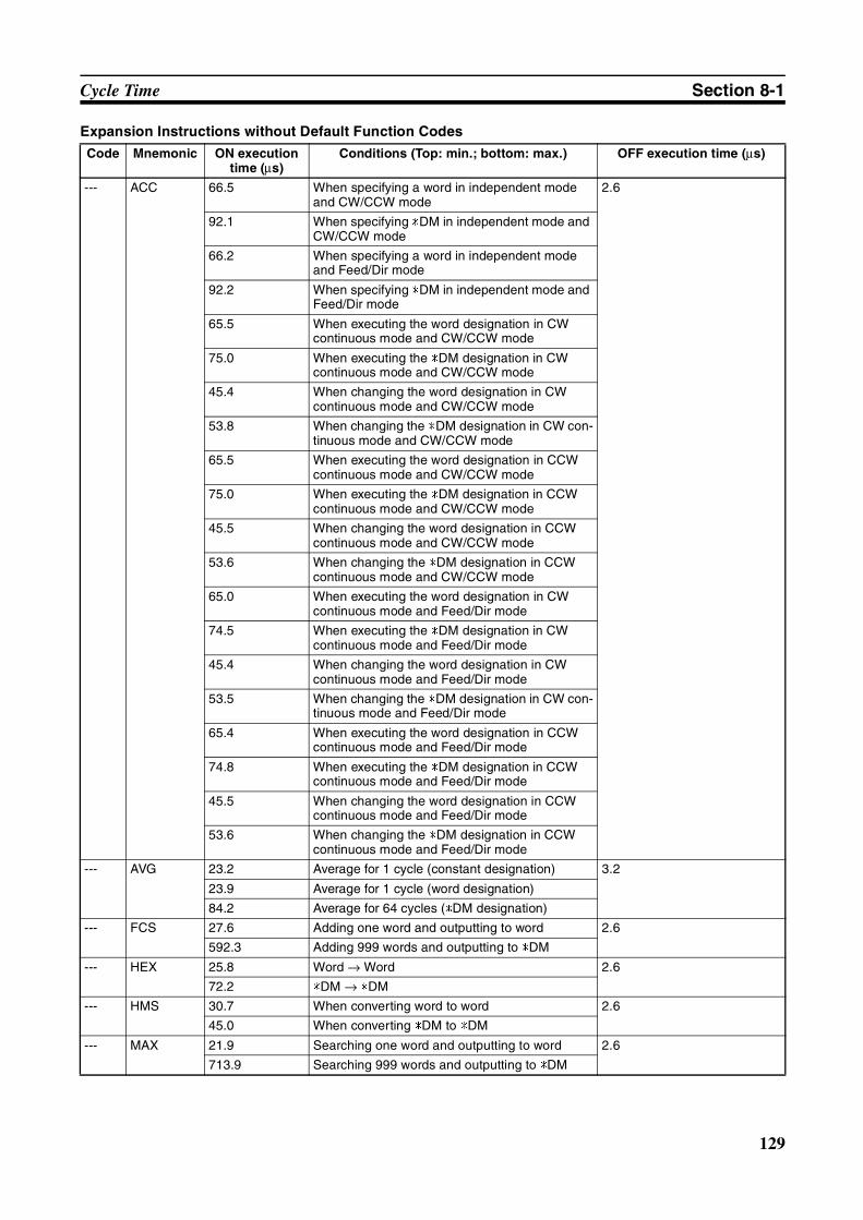
129
Cycle Time Section 8-1
Expansion Instructions without Default Function Codes
Code Mnemonic ON execution time (µs)
Conditions (Top: min.; bottom: max.) OFF execution time (µs)
--- ACC 66.5 When specifying a word in independent mode and CW/CCW mode
2.6
92.1 When specifying *DM in independent mode and CW/CCW mode
66.2 When specifying a word in independent mode and Feed/Dir mode
92.2 When specifying *DM in independent mode and Feed/Dir mode
65.5 When executing the word designation in CW continuous mode and CW/CCW mode
75.0 When executing the *DM designation in CW continuous mode and CW/CCW mode
45.4 When changing the word designation in CW continuous mode and CW/CCW mode
53.8 When changing the *DM designation in CW con-tinuous mode and CW/CCW mode
65.5 When executing the word designation in CCW continuous mode and CW/CCW mode
75.0 When executing the *DM designation in CCW continuous mode and CW/CCW mode
45.5 When changing the word designation in CCW continuous mode and CW/CCW mode
53.6 When changing the *DM designation in CCW continuous mode and CW/CCW mode
65.0 When executing the word designation in CW continuous mode and Feed/Dir mode
74.5 When executing the *DM designation in CW continuous mode and Feed/Dir mode
45.4 When changing the word designation in CW continuous mode and Feed/Dir mode
53.5 When changing the *DM designation in CW con-tinuous mode and Feed/Dir mode
65.4 When executing the word designation in CCW continuous mode and Feed/Dir mode
74.8 When executing the *DM designation in CCW continuous mode and Feed/Dir mode
45.5 When changing the word designation in CCW continuous mode and Feed/Dir mode
53.6 When changing the *DM designation in CCW continuous mode and Feed/Dir mode
--- AVG 23.2 Average for 1 cycle (constant designation) 3.2
23.9 Average for 1 cycle (word designation)
84.2 Average for 64 cycles (*DM designation)
--- FCS 27.6 Adding one word and outputting to word 2.6
592.3 Adding 999 words and outputting to *DM
--- HEX 25.8 Word → Word 2.6
72.2 *DM → *DM
--- HMS 30.7 When converting word to word 2.6
45.0 When converting *DM to *DM
--- MAX 21.9 Searching one word and outputting to word 2.6
713.9 Searching 999 words and outputting to *DM
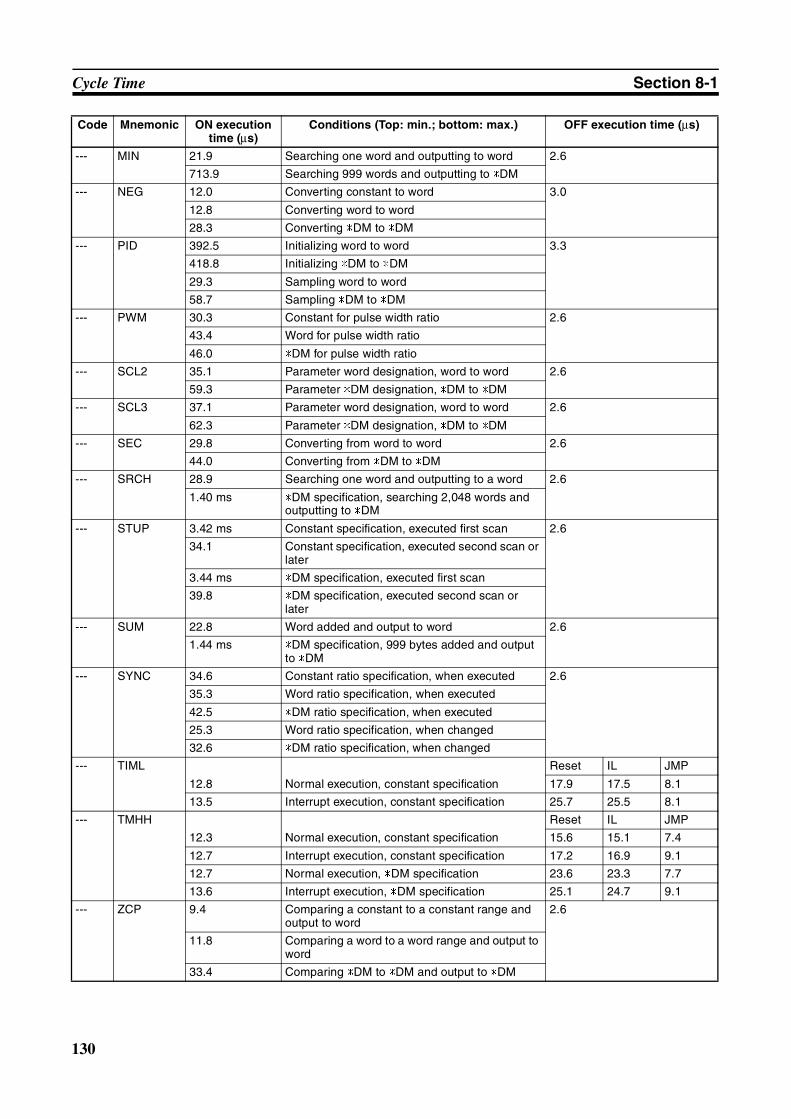
130
Cycle Time Section 8-1
--- MIN 21.9 Searching one word and outputting to word 2.6
713.9 Searching 999 words and outputting to *DM
--- NEG 12.0 Converting constant to word 3.0
12.8 Converting word to word
28.3 Converting *DM to *DM
--- PID 392.5 Initializing word to word 3.3
418.8 Initializing *DM to *DM
29.3 Sampling word to word
58.7 Sampling *DM to *DM
--- PWM 30.3 Constant for pulse width ratio 2.6
43.4 Word for pulse width ratio
46.0 *DM for pulse width ratio
--- SCL2 35.1 Parameter word designation, word to word 2.6
59.3 Parameter *DM designation, *DM to *DM
--- SCL3 37.1 Parameter word designation, word to word 2.6
62.3 Parameter *DM designation, *DM to *DM
--- SEC 29.8 Converting from word to word 2.6
44.0 Converting from *DM to *DM
--- SRCH 28.9 Searching one word and outputting to a word 2.6
1.40 ms *DM specification, searching 2,048 words and outputting to *DM
--- STUP 3.42 ms Constant specification, executed first scan 2.6
34.1 Constant specification, executed second scan or later
3.44 ms *DM specification, executed first scan
39.8 *DM specification, executed second scan or later
--- SUM 22.8 Word added and output to word 2.6
1.44 ms *DM specification, 999 bytes added and output to *DM
--- SYNC 34.6 Constant ratio specification, when executed 2.6
35.3 Word ratio specification, when executed
42.5 *DM ratio specification, when executed
25.3 Word ratio specification, when changed
32.6 *DM ratio specification, when changed
--- TIML Reset IL JMP
12.8 Normal execution, constant specification 17.9 17.5 8.1
13.5 Interrupt execution, constant specification 25.7 25.5 8.1
--- TMHH Reset IL JMP
12.3 Normal execution, constant specification 15.6 15.1 7.4
12.7 Interrupt execution, constant specification 17.2 16.9 9.1
12.7 Normal execution, *DM specification 23.6 23.3 7.7
13.6 Interrupt execution, *DM specification 25.1 24.7 9.1
--- ZCP 9.4 Comparing a constant to a constant range and output to word
2.6
11.8 Comparing a word to a word range and output to word
33.4 Comparing *DM to *DM and output to *DM
Code Mnemonic ON execution time (µs)
Conditions (Top: min.; bottom: max.) OFF execution time (µs)
131
I/O Response Time Section 8-2
8-2 I/O Response Time
8-2-1 CPM2B-S I/O Response TimeThe I/O response time is the time it takes after an input signal has beenreceived (i.e., after an input bit has turned ON) for the PC to check and pro-cess the information and to output a control signal (i.e., to output the result ofthe processing to an output bit). The I/O response time varies according to thetiming and processing conditions.
The minimum and maximum I/O response times are shown here, using thefollowing program as an example.
The following conditions are taken as examples for calculating the I/Oresponse times.
Input ON delay: 10 ms (input time constant: default setting)Overseeing time: 1 ms (includes I/O refreshing)Instruction execution time: 14 msOutput ON delay: 15 msCommunications ports: Not used.
Minimum I/O Response Time
The CPM2B-S responds most quickly when it receives an input signal justprior to I/O refreshing, as shown in the illustration below.
--- ZCPL 19.5 Comparing a word to a word range 2.6
45.2 Comparing *DM to *DM
Code Mnemonic ON execution time (µs)
Conditions (Top: min.; bottom: max.) OFF execution time (µs)
InputOutput
Input ON delay (10 ms)
I/O refreshing
Input point
Input bit
Output point
I/O refreshingProgram execution and other processes (15 ms)
Min. I/O response time = 10 + 15 + 15 = 40 ms
Output ON delay (15 ms)
132
I/O Response Time Section 8-2
Maximum I/O Response Time
The CPM2B-S takes longest to respond when it receives the input signal justafter the input refresh phase of the cycle, as shown in the illustration below. Inthat case, a delay of approximately one cycle will occur.
8-2-2 I/O Response Time between CompoBus/S SlavesThe I/O response time between CompoBus/S Slaves depends on the cycletime and I/O timing.
Minimum I/O Response Time
The minimum I/O response time is the CPM2B-S program execution time plusthe cycle time calculation time.
Input ON delay (10 ms)
I/O refreshing
Input point
Input bit
Output point
Program execution and other processes
(15 ms)
Max. I/O response time = 10+15 × 2+15 = 55 ms
Output ON delay (15 ms)
I/O refreshingProgram execution
and other processes (15 ms)
I/O refreshing
CompoBus/S transmission line
CompoBus/S Slaves
CPM2B-S
CPM2B-S cycle
CompoBus/S communications processing
Slave input
Slave output
CompoBus/S input refreshing
CompoBus/S output refreshing
CompoBus/S communica-tions time
CompoBus/S communica-tions time
Input delay
Output delay
133
Interrupt Processing Time Section 8-3
Maximum I/O Response Time
The maximum I/O response time is as follows:(2 × CPM2B-S cycle time) + CompoBus/S communications time + Compo-Bus/S Slave input delay + CompoBus/S Slave output delay
Note The Slave input is not read for almost one PC cycle because it goes ON justafter the start of CompoBus/S communications processing (*1). The input isread during the next CompoBus/S communications processing cycle (*2).
8-3 Interrupt Processing TimeThis section explains the processing times involved from the time an interruptis executed until the interrupt processing routine is called, and from the timean interrupt processing routine is completed until returning to the initial loca-tion. This explanation applies to input interrupts, interval timer interrupts, andhigh-speed counter interrupts.
1,2,3... 1. Interrupt source
2. Interrupt ON delay
3. Wait for completion of interrupt-mask processing
4. Change to interrupt processing
5. Execution of interrupt routine
6. Return to initial location
The table below shows the times involved from the generation of an interruptsignal until the interrupt processing routine is called, and from when the inter-rupt processing routine is completed until returning to the original position.
Mask Processing
Interrupts are masked during processing of the operations described below.Until the processing is completed, any interrupts will remain masked for theindicated times.
CPM2B-S cycle
CompoBus/S communications processing
Slave input
Slave output
CompoBus/S input refreshing
CompoBus/S output refreshing
CompoBus/S communica-tions time
Input delay
Output delay
Cycle time (See note 1.) Cycle time (See note 2.)
(See note 2.)
CompoBus/S communica-tions time
CompoBus/S communica-tions time
Item Contents Time
Interrupt ON delay This is the delay time from the time the interrupt input bit turns ON until the time that the interrupt is executed. This delay does not apply to other interrupts.
50 µs
Wait for completion ofinterrupt-mask processing
When a process that disables (masks) the interrupt is being executed, this is the time required for that process to be completed.
Seebelow.
Change to interruptprocessing
This is the time it takes to change processing to the interrupt process. 10 µs
Return This is the time it takes, from execution of RET(93), to return to the processing that was interrupted.
10 µs
134
One-to-one PC Link I/O Response Time Section 8-4
Generation and clearing of non-fatal errors:
Interrupts will be masked for up to 100 µs when a non-fatal error has beengenerated and the error contents are being registered in the PC, or whenan error is being cleared.
Online editing:
Operation will stop and interrupts will be masked for up to 600 ms (forDM 6144 to DM 6655) when online editing is executed or the settings arechanged with STUP(– –) during operation. The program or PC Setup canbe overwritten during that delay.
In addition to the online editing delay, interrupts may be masked for up to150 µs for system processing.
Example Calculation This example shows the interrupt response time (i.e., the time from when theinterrupt input turns ON until the start of the interrupt processing routine)when input interrupts are used under the conditions shown below.
Minimum Response Time
Interrupt ON delay: 50 µsInterrupt mask standby time: 0 µs
+ Change-to-interrupt processing: 10 µsMinimum response time: 60 µs
Maximum Response Time (Except for the Online Editing of DM 6144 to DM 6655)
Interrupt ON delay: 50 µsInterrupt mask standby time: 150 µs
+ Change-to-interrupt processing: 10 µsMaximum response time: 210 µs
In addition to the response time shown above, the time required for executingthe interrupt processing routine itself and a return time of 10 µs must also beaccounted for when returning to the process that was interrupted.
8-4 One-to-one PC Link I/O Response TimeWhen two CPM2B-S PCs are linked 1:1, the I/O response time is the timerequired for an input executed at one of the PCs to be output to the other PCby means of 1:1 PC Link communications.
The minimum and maximum I/O response times are shown here, using as anexample the following instructions executed at the master and the slave. Inthis example, communications proceed from the master to the slave.
InputOutput (LR) Input
(LR)Output
Master Slave
135
One-to-one PC Link I/O Response Time Section 8-4
The following conditions are taken as examples for calculating the I/Oresponse times. In CPM2B-S PCs, LR area words LR 00 to LR 15 are used in1:1 data links and the transmission time is fixed at 12 ms.
Input ON delay: 10 ms (input time constant: default setting)Master cycle time: 10 msSlave cycle time: 15 msOutput ON delay: 15 ms
Minimum I/O Response Time
The CPM2B-S responds most quickly under the following circumstances:
1,2,3... 1. The CPM2B-S receives an input signal just prior to the input refresh phaseof the cycle.
2. The Master’s communications servicing occurs just as the Master-to-Slavetransmission begins.
3. The Slave’s communications servicing occurs just after the transmission iscompleted.
The minimum I/O response time = Input ON response time + Master’s cycletime + Transmission time + Slave’s cycle time + Output ON response time
Maximum I/O Response Time
The CPM2B-S takes the longest to respond under the following circum-stances:
1,2,3... 1. The CPM2B-S receives an input signal just after the input refresh phase ofthe cycle.
2. The Master’s communications servicing just misses the Master-to-Slavetransmission.
3. The transmission is completed just after the Slave’s communications ser-vicing ends.
Output point
Master's cycle time (10 ms)
Program execution
Transmission time (12 ms)
Slave's cycle time (15 ms)
Min. I/O response time = 10+10+12+15+15 = 62 ms
Input point
Input bit
I/O refresh
Overseeing, communications servicing, etc.
Input ON delay (10 ms)
Master to Slave
Output ON delay (15 ms)
Program execution
CPUprocessing
CPUprocessing
Master
Slave
136
One-to-one PC Link I/O Response Time Section 8-4
The maximum I/O response time = Input ON response time + Master’s cycletime × 2 + Transmission time × 3 + Slave’s cycle time × 2 + Output ONresponse time
Output point
Master's cycle time (10 ms)
Programexecution
Transmission time (12 ms × 3)
Slave's cycle time (15 ms)
Input point
Input bit
I/O refresh
Overseeing, communications servicing, etc.
Input ON delay (10 ms)
Output ON delay (15 ms)
CPUprocessing
Programexecution
Master to Slave
Master to Slave
Master to Slave
Programexecution
Programexecution
Maximum I/O response time = 10 + 10 × 2 + 12 × 3 + 15 × 2 + 15 = 111 (ms)
137
SECTION 9Test Runs and Error Processing
This section describes procedures for test runs of CPM2B-S operation, self-diagnosis functions, and error processing toidentify and correct the hardware and software errors that can occur during PC operation.
9-1 Initial System Checks and Test Run Procedure . . . . . . . . . . . . . . . . . . . . . . . 138
9-1-1 Initial System Checks . . . . . . . . . . . . . . . . . . . . . . . . . . . . . . . . . . . . 138
9-1-2 Flash Memory Precautions . . . . . . . . . . . . . . . . . . . . . . . . . . . . . . . . 138
9-2 CPM2B-S Test Run Procedure . . . . . . . . . . . . . . . . . . . . . . . . . . . . . . . . . . . . 138
9-3 Self-diagnostic Functions . . . . . . . . . . . . . . . . . . . . . . . . . . . . . . . . . . . . . . . . 139
9-3-1 Identifying Errors . . . . . . . . . . . . . . . . . . . . . . . . . . . . . . . . . . . . . . . 139
9-3-2 User-defined Errors. . . . . . . . . . . . . . . . . . . . . . . . . . . . . . . . . . . . . . 140
9-3-3 Non-fatal Errors . . . . . . . . . . . . . . . . . . . . . . . . . . . . . . . . . . . . . . . . 141
9-3-4 Fatal Errors . . . . . . . . . . . . . . . . . . . . . . . . . . . . . . . . . . . . . . . . . . . . 142
9-4 Troubleshooting Flowcharts . . . . . . . . . . . . . . . . . . . . . . . . . . . . . . . . . . . . . . 143
9-5 Maintenance Inspections. . . . . . . . . . . . . . . . . . . . . . . . . . . . . . . . . . . . . . . . . 151
9-6 Battery Replacement . . . . . . . . . . . . . . . . . . . . . . . . . . . . . . . . . . . . . . . . . . . . 151
138
Initial System Checks and Test Run Procedure Section 9-1
9-1 Initial System Checks and Test Run Procedure
9-1-1 Initial System ChecksCheck the following items after setting up and wiring the CPM2B-S, but beforeperforming a test run.
Clearing Memory Always clear memory before beginning to program the CPM2B-S. Althoughmemory is cleared before the CPU Board is shipped, the contents of the DM,HR, AR, and counter areas may change in transit.
Operating Mode at Startup See 1-3-3 Operating Mode at Startup to determine what mode the CPM2B-Swill enter when the power is turned on.
9-1-2 Flash Memory PrecautionsObserve the following precautions to protect the flash memory and ensureproper operation.
1,2,3... 1. If changes are made in the read-only DM area (DM 6144 through DM6599) or PC Setup (DM 6600 through DM 6655), the PC’s operating modemust be changed to write the new contents to flash memory. If backup bat-tery is replaced before the changes are written to flash memory, the chang-es will be lost.The changes can be saved by switching the CPM2B-S to RUN or MONI-TOR mode or turning the CPM2B-S OFF and then ON again.
2. When contents of the program, read-only DM (DM 6144 through DM6599), or PC Setup (DM 6600 through DM 6655) have been changed, star-tup processing will take up to 1,200 ms longer than usual. Be sure to takethis one-time startup delay into account if it may affect operations.
3. If one of the following three operations is performed in MONITOR or RUNmode, the CPM2B-S’s cycle time will be extended by up to 1,200 ms andinterrupts will be disabled while the program or PC Setup is being overwrit-ten.
• Program changes with the online edit operation• Changes to the read-only DM area (DM 6144 through DM 6599)• Changes to the PC Setup (DM 6600 through DM 6655)
A “SCAN TIME OVER” error won’t occur during these operations. Be sureto take this delay in the CPM2B-S’s I/O response times into account whenperforming online editing.
9-2 CPM2B-S Test Run Procedure1,2,3... 1. Power Supply Application
a) Check the CPM2B-S’s power supply voltage and terminal connec-tions.
b) Check the I/O devices’ power supply voltage and terminal connec-tions.
c) Turn on the power supply and check that the “PWR” indicator lights.
d) Use a Programming Device to set the CPM2B-S to PROGRAM mode.
Item Points to check
Power supply and I/O connections
Is the wiring correct?Are the terminals securely tightened?Are there any shorts between crimp terminals or wires?
Refer to 3-5 Wiring and Connections for details.
Connecting cables Are the cables all connected correctly and locked?
Refer to 3-5 Wiring and Connections for details.
139
Self-diagnostic Functions Section 9-3
2. I/O Wiring Checksa) With the CPM2B-S in PROGRAM mode, check the output wiring by
turning on the output bits with the force set and force reset operations.b) Check the input wiring with the CPM2B-S’s input indicators or a Pro-
gramming Device’s monitor operations.3. Test Run
a) Use a Programming Device to set the CPM2B-S to RUN or MONITORmode and check that the “RUN” indicator lights.
b) Check the sequence of operation with the force set/reset operations,etc.
4. DebuggingCorrect any programming errors that are detected.
5. Saving the Programa) Use a Programming Device to write the program to a backup floppy
disk.b) Print out a hard copy of the program with a printer.
Note Refer to Section 4 Using Programming Devices for details on the SupportSoftware and Programming Console operations.
9-3 Self-diagnostic FunctionsThe CPM2B-S is equipped with a variety of self-diagnostic functions to helpidentify and correct errors and reduce down time.
9-3-1 Identifying ErrorsAn error can be identified by the error message displayed on a ProgrammingDevice, error flags in the AR and SR areas, and the error code output toSR 253.
Fatal and Non-fatal Errors PC errors are divided into 2 categories based on the severity of the errors.The status of the ERR indicator (lit or flashing) shows which type of error hasoccurred.
ERR Lit (Fatal Error)Fatal errors are serious errors which stop CPM2B-S operation. There are twoways to restart operation:
• Turn the PC off and then on again.• Use a Programming Device to switch the PC to PROGRAM mode, and
read/clear the error.
ERR Flashing (Non-fatal Error)Non-fatal errors are less serious errors which don’t stop CPM2B-S operation.
Communications Errors The LED indicators and AR area flags indicate when a CompoBus/S commu-nications error, RS-232C port error, or peripheral port error has occurred.
CompoBus/S Communications Error
When an error occurs in CompoBus/S communications, the SD and RD indi-cators will be OFF and the ERC indicator will be ON. Check the Slaves andthe transmission lines and restart communications.
RS-232C Port Error
When an error occurs in communications through the RS-232C port, theCOMM indicator will be OFF and the RS-232C Communications Error Flag(AR 0804) will be ON. Check the cables and restart communications.
140
Self-diagnostic Functions Section 9-3
Peripheral Port Error
When an error occurs in communications through the peripheral port, theCOMM indicator will be OFF and the Peripheral Port Communications ErrorFlag (AR 0812) will be ON. Check the cables and restart communications.
Error Messages When an error is detected, a corresponding error message will be displayedon the Programming Console or other Programming Device connected to thePC.
Error Flags When a hardware error is detected, the corresponding error flag in the AR orSR area will be turned ON.
Error Code When an error is detected, a specific 2-digit hexadecimal error code is outputto SR 25300 to SR 25307. The error code and time of occurrence are alsooutput to the Error Log Area (DM 2000 to DM 2021).
!WARNING When the CPM2B-S’s self-diagnosis function detects a fatal error or when asevere failure alarm (FALS) instruction is executed, PC operation will stop andall outputs will be turned OFF. External safety measures must be provided toensure safety in the system. Not providing proper safety measures may resultin serious accidents.
!WARNING Emergency stop circuits, interlock circuits, limit circuits, and similar safetymeasures must be provided in external control circuits (i.e., not in the Pro-grammable Controller) to ensure safety in the system if an abnormality occursdue to malfunction of the PC or another external factor affecting the PC oper-ation. Not providing proper safety measures may result in serious accidents.
9-3-2 User-defined ErrorsThere are three instructions that can be used to define errors or messages.FAL(06) causes a non-fatal error, FAL(07) causes a fatal error, and MSG(46)sends a message to the Programming Console or host computer connectedto the PC.
FAILURE ALARM – FAL(06)
FAL(06) is an instruction that causes a non-fatal error. The following will occurwhen an FAL(06) instruction is executed:
1,2,3... 1. The ERR indicator on the CPU Board will flash. PC operation will continue.
2. The instruction’s 2-digit BCD FAL number (01 to 99) will be written toSR 25300 to SR 25307.
The FAL numbers can be set arbitrarily to indicate particular conditions, butthe same number should not be used as both an FAL number and an FALSnumber.To clear an FAL error, correct the cause of the error and then execute FAL 00or use a Programming Device to clear the error.
SEVERE FAILURE ALARM – FALS(07)
FALS(07) is an instruction that causes a fatal error. The following will occurwhen an FALS(07) instruction is executed:
1,2,3... 1. Program execution will be stopped and all outputs will be turned OFF.
2. The ERR indicator on the CPU Board will be lit.
3. The instruction’s 2-digit BCD FALS number (01 to 99) will be written toSR 25300 to SR 25307.
The FALS numbers can be set arbitrarily to indicate particular conditions, butthe same number should not be used as both an FAL number and an FALSnumber.
To clear an FALS error, use a Programming Device to switch the PC to PRO-GRAM Mode, correct the cause of the error, and then clear the error.
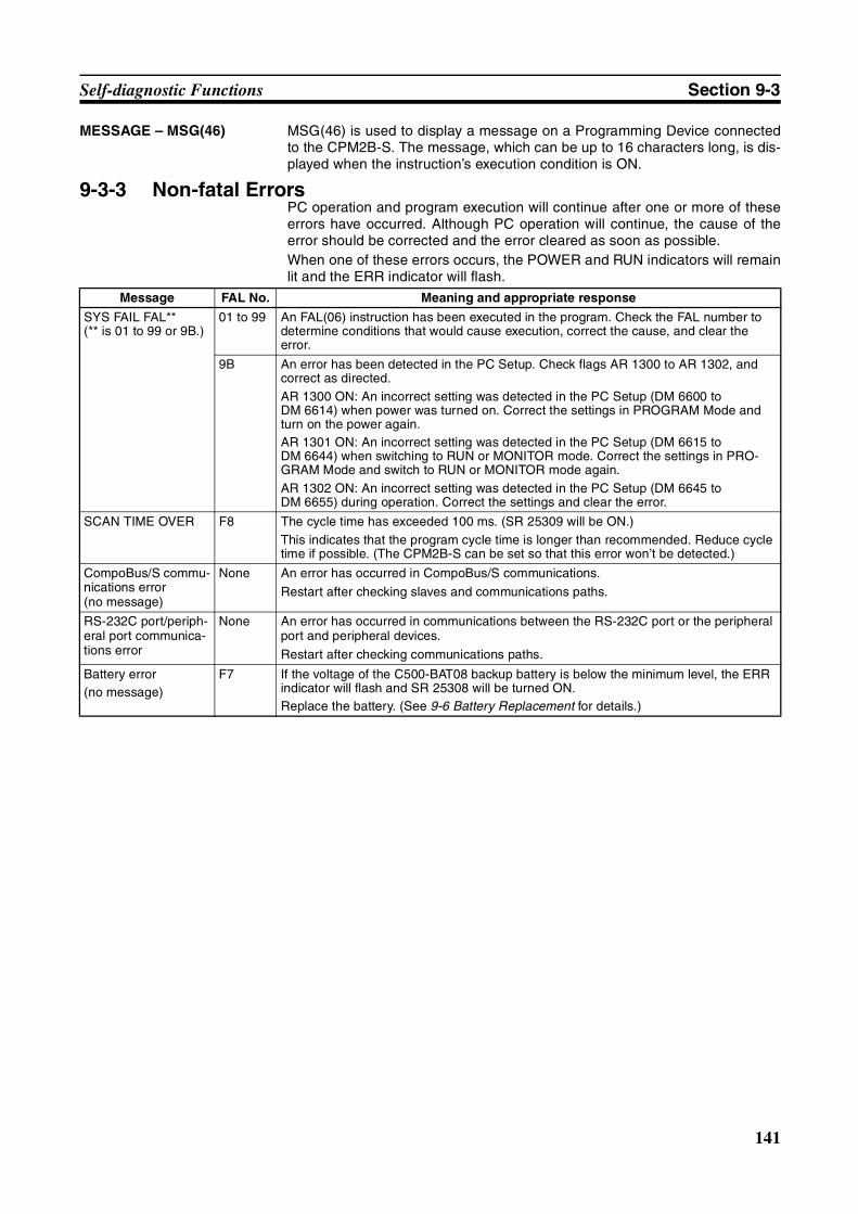
141
Self-diagnostic Functions Section 9-3
MESSAGE – MSG(46) MSG(46) is used to display a message on a Programming Device connectedto the CPM2B-S. The message, which can be up to 16 characters long, is dis-played when the instruction’s execution condition is ON.
9-3-3 Non-fatal ErrorsPC operation and program execution will continue after one or more of theseerrors have occurred. Although PC operation will continue, the cause of theerror should be corrected and the error cleared as soon as possible.When one of these errors occurs, the POWER and RUN indicators will remainlit and the ERR indicator will flash.
Message FAL No. Meaning and appropriate response
SYS FAIL FAL**(** is 01 to 99 or 9B.)
01 to 99 An FAL(06) instruction has been executed in the program. Check the FAL number to determine conditions that would cause execution, correct the cause, and clear the error.
9B An error has been detected in the PC Setup. Check flags AR 1300 to AR 1302, and correct as directed.AR 1300 ON: An incorrect setting was detected in the PC Setup (DM 6600 to DM 6614) when power was turned on. Correct the settings in PROGRAM Mode and turn on the power again.AR 1301 ON: An incorrect setting was detected in the PC Setup (DM 6615 to DM 6644) when switching to RUN or MONITOR mode. Correct the settings in PRO-GRAM Mode and switch to RUN or MONITOR mode again.AR 1302 ON: An incorrect setting was detected in the PC Setup (DM 6645 to DM 6655) during operation. Correct the settings and clear the error.
SCAN TIME OVER F8 The cycle time has exceeded 100 ms. (SR 25309 will be ON.)This indicates that the program cycle time is longer than recommended. Reduce cycle time if possible. (The CPM2B-S can be set so that this error won’t be detected.)
CompoBus/S commu-nications error(no message)
None An error has occurred in CompoBus/S communications.
Restart after checking slaves and communications paths.
RS-232C port/periph-eral port communica-tions error
None An error has occurred in communications between the RS-232C port or the peripheral port and peripheral devices.
Restart after checking communications paths.
Battery error(no message)
F7 If the voltage of the C500-BAT08 backup battery is below the minimum level, the ERR indicator will flash and SR 25308 will be turned ON.Replace the battery. (See 9-6 Battery Replacement for details.)
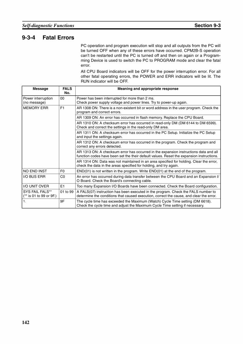
142
Self-diagnostic Functions Section 9-3
9-3-4 Fatal ErrorsPC operation and program execution will stop and all outputs from the PC willbe turned OFF when any of these errors have occurred. CPM2B-S operationcan’t be restarted until the PC is turned off and then on again or a Program-ming Device is used to switch the PC to PROGRAM mode and clear the fatalerror.
All CPU Board indicators will be OFF for the power interruption error. For allother fatal operating errors, the POWER and ERR indicators will be lit. TheRUN indicator will be OFF.
Message FALS No.
Meaning and appropriate response
Power interruption(no message)
00 Power has been interrupted for more than 2 ms.Check power supply voltage and power lines. Try to power-up again.
MEMORY ERR F1 AR 1308 ON: There is a non-existent bit or word address in the user program. Check the program and correct errors.
AR 1309 ON: An error has occurred in flash memory. Replace the CPU Board.
AR 1310 ON: A checksum error has occurred in read-only DM (DM 6144 to DM 6599). Check and correct the settings in the read-only DM area.
AR 1311 ON: A checksum error has occurred in the PC Setup. Initialize the PC Setup and input the settings again.
AR 1312 ON: A checksum error has occurred in the program. Check the program and correct any errors detected.
AR 1313 ON: A checksum error has occurred in the expansion instructions data and all function codes have been set the their default values. Reset the expansion instructions.
AR 1314 ON: Data was not maintained in an area specified for holding. Clear the error, check the data in the areas specified for holding, and try again.
NO END INST F0 END(01) is not written in the program. Write END(01) at the end of the program.
I/O BUS ERR C0 An error has occurred during data transfer between the CPU Board and an Expansion I/O Board. Check the Board’s connecting cable.
I/O UNIT OVER E1 Too many Expansion I/O Boards have been connected. Check the Board configuration.
SYS FAIL FALS**(** is 01 to 99 or 9F.)
01 to 99 A FALS(07) instruction has been executed in the program. Check the FALS number to determine the conditions that caused execution, correct the cause, and clear the error.
1. 9F The cycle time has exceeded the Maximum (Watch) Cycle Time setting (DM 6618). Check the cycle time and adjust the Maximum Cycle Time setting if necessary.
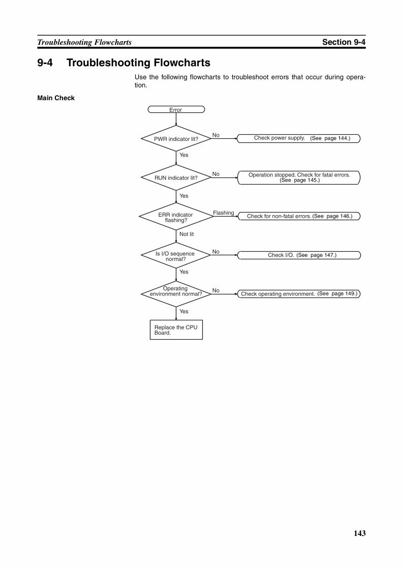
143
Troubleshooting Flowcharts Section 9-4
9-4 Troubleshooting FlowchartsUse the following flowcharts to troubleshoot errors that occur during opera-tion.
Main Check
Operation stopped. Check for fatal errors.
Check for non-fatal errors.
Error
Replace the CPU Board.
PWR indicator lit?
RUN indicator lit?
ERR indicator flashing?
Is I/O sequence normal?
Operating environment normal?
Check I/O.
Check operating environment.
Yes
Check power supply. No
No
No
No
Flashing
Yes
Yes
Not lit
Yes
(See page 144.)
(See page 145.)
(See page 146.)
(See page 147.)
(See page 149.)
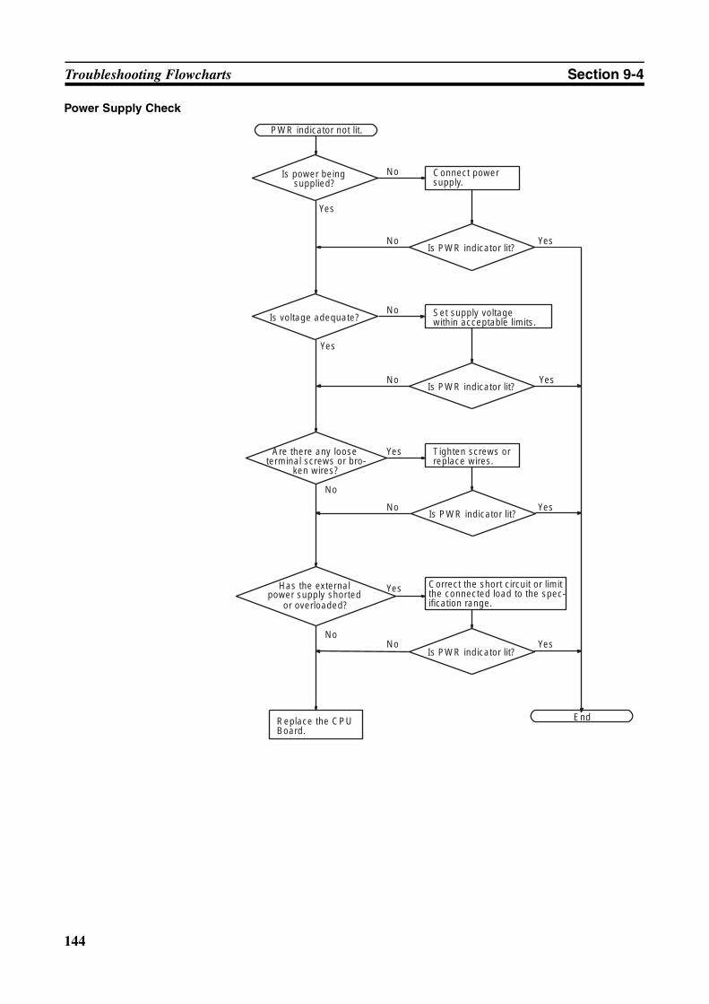
144
Troubleshooting Flowcharts Section 9-4
Power Supply Check
PWR indicator not lit.
Replace the CPU Board.
Is power being supplied?
Is voltage adequate?
Are there any loose terminal screws or bro-
ken wires?
Connect power supply.
Is PWR indicator lit?
Set supply voltage within acceptable limits.
Is PWR indicator lit?
Tighten screws or replace wires.
End
Yes
No
No Yes
YesNo
No
NoIs PWR indicator lit?
Yes
No
Yes
Yes
Has the external power supply shorted
or overloaded?
Correct the short circuit or limit the connected load to the spec-ification range.
NoNo
Is PWR indicator lit?Yes
Yes
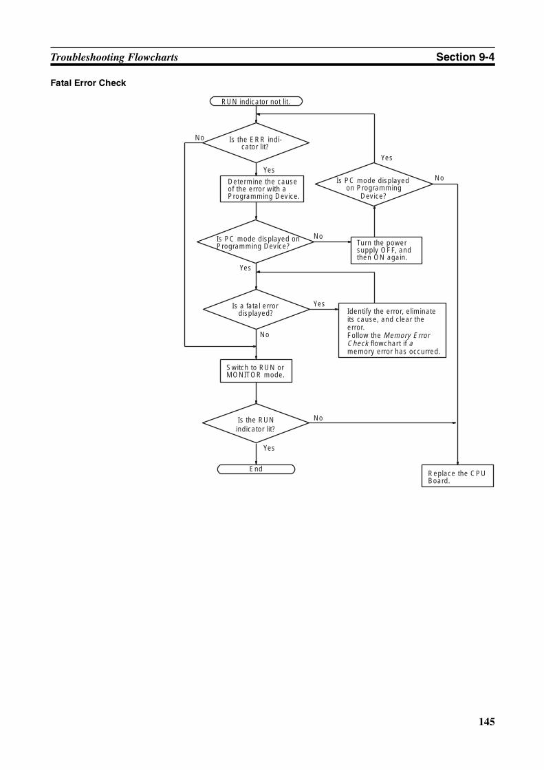
145
Troubleshooting Flowcharts Section 9-4
Fatal Error Check
Identify the error, eliminate its cause, and clear the error.Follow the Memory Error Check flowchart if a memory error has occurred.
Is the ERR indi-cator lit?
Determine the cause of the error with a Programming Device.
End
RUN indicator not lit.
Replace the CPU Board.
Is PC mode displayed on Programming
Device?
Turn the power supply OFF, and then ON again.
Switch to RUN or MONITOR mode.
No
Yes
Is a fatal error displayed?
Is PC mode displayed on Programming Device?
No
Yes
Yes
No
Is the RUNindicator lit?
No
Yes
Yes
No
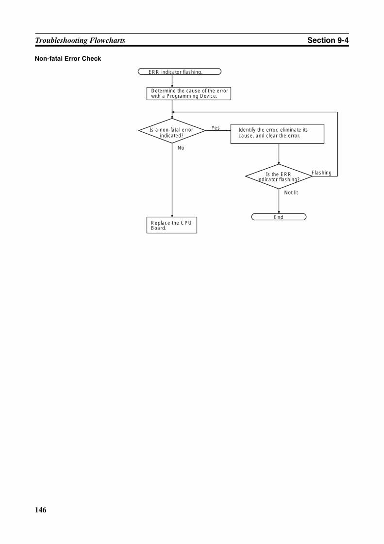
146
Troubleshooting Flowcharts Section 9-4
Non-fatal Error Check
Identify the error, eliminate its cause, and clear the error.
Is a non-fatal error indicated?
Is the ERRindicator flashing?
Replace the CPU Board.
End
Determine the cause of the error with a Programming Device.
No
Yes
Flashing
Not lit
ERR indicator flashing.
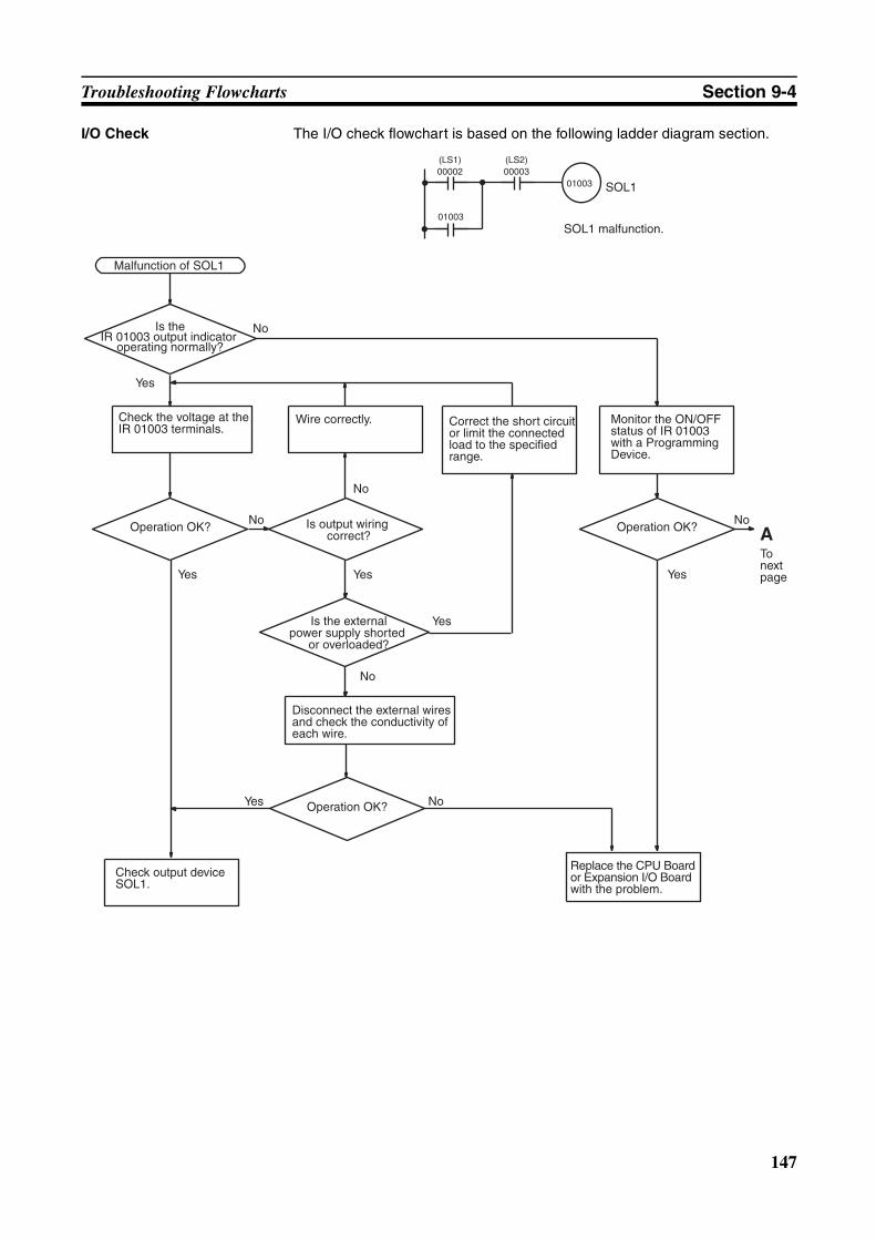
147
Troubleshooting Flowcharts Section 9-4
I/O Check The I/O check flowchart is based on the following ladder diagram section.
0100300002(LS1)
00003(LS2)
SOL1 malfunction.
SOL1
01003
Yes
Monitor the ON/OFF status of IR 01003 with a Programming Device.
NoIs theIR 01003 output indicator
operating normally?
Check the voltage at the IR 01003 terminals.
Wire correctly.
Operation OK? Operation OK?Is output wiring correct?
Disconnect the external wires and check the conductivity of each wire.
No
Yes
Check output device SOL1.
Replace the CPU Board or Expansion I/O Board with the problem.
Yes
No No
Operation OK? NoYes
Yes
ATo next page
Malfunction of SOL1
Is the externalpower supply shorted
or overloaded?
Yes
No
Correct the short circuit or limit the connected load to the specified range.
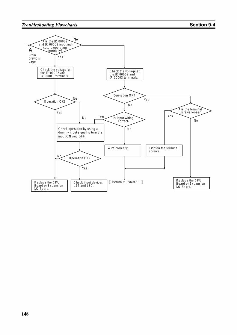
148
Troubleshooting Flowcharts Section 9-4
Yes
No
Check the voltage at the IR 00002 and IR 00003 terminals.
Check operation by using a dummy input signal to turn the input ON and OFF.
No
Are the terminal screws loose?
Operation OK?
Check input devices LS1 and LS2.
Operation OK?
Wire correctly.
Is input wiring correct?
Tighten the terminal screws
Return to "start."
Are the IR 00002 and IR 00003 input indi-
cators operating normally?
Replace the CPU Board or Expansion I/O Board.
Yes
Yes
Yes
Yes
NoNo
No
No
No
No
No
Check the voltage at the IR 00002 and IR 00003 terminals.
AFrom previous page
Yes
Replace the CPU Board or Expansion I/O Board.
Operation OK?
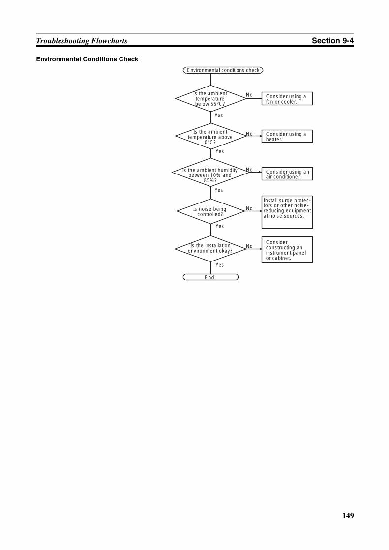
149
Troubleshooting Flowcharts Section 9-4
Environmental Conditions Check
Consider using a fan or cooler.
Environmental conditions check
Is the ambient temperature below 55°C?
Is the ambient temperature above
0°C?
Is noise being controlled?
Is the installationenvironment okay?
Consider using a heater.
Consider using an air conditioner.
Install surge protec-tors or other noise-reducing equipment at noise sources.
Consider constructing an instrument panel or cabinet.
End.
Yes
No
Yes
No
No
No
No
Yes
Yes
Yes
Is the ambient humidity between 10% and
85%?
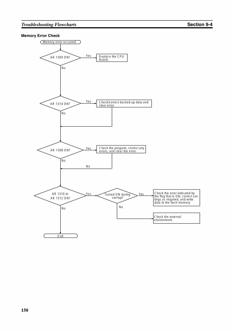
150
Troubleshooting Flowcharts Section 9-4
Memory Error Check
Memory error occurred.
AR 1309 ON?
AR 1314 ON?
AR 1308 ON?
Replace the CPU Board.
Check/correct backed-up data and clear error.
Check the program, correct any errors, and clear the error.
End
No
Yes
No
No
Yes
No
Yes
AR 1310 to AR 1312 ON?
Check the error indicated by the flag that is ON, correct set-tings as required, and write data to the flash memory.
No
Turned ON during startup?
YesYes
Check the external environment.
No
151
Maintenance Inspections Section 9-5
9-5 Maintenance InspectionsIn order for your SYSMAC system to operate in optimum condition, be sure tocarry out daily or periodical inspections.
Inspection Items The main system components of a SYSMAC system are semiconductors, andit contains few components with limited lifetimes. Poor environmental condi-tions, however, can lead to deterioration of the electrical components, makingregular maintenance necessary.
The standard period for maintenance checks is 6 months to 1 year, but morefrequent checks are required if the PC is operated in more demanding condi-tions.
If the criteria are not met, adjust to within the specified ranges.
Required Tools Standard Tools (Required)
• Screwdrivers (Phillips and flat-blade)
• Voltage tester or digital voltage meter
• Industrial alcohol and a cotton cloth
Measurement Devices (May be Needed)
• Synchroscope
• Cathode-ray oscilloscope
• Thermometer, hygrometer
Note Do not attempt to disassemble, repair, or modify the PC in any way.
9-6 Battery Replacement
!WARNING Do not drop, disassemble, crush, short-circuit, recharge, or dispose of the bat-tery in fire. The battery may explode, burn, or leak and cause personal injury.
Inspection items Details Criteria Remarks
Power supply Determine whether the voltage fluctuation at the power supply terminals is within specifications.
Within the voltage variation range (20.4 to 26.4 VDC)
Tester
Environmental conditions
Is the ambient temperature inside the panel appropriate?
0 to 55°C Thermometer
Is the ambient humidity inside the panel appropriate?
35% to 85% RH with no condensation
Hygrometer
Has dirt or dust collected? None Visual inspection
I/O power supply Is the voltage fluctuation measured at the I/O terminals within the standard range?
Each I/O terminal must conform to the specifications
Tester
Installation status Are all Boards securely installed? Nothing is loose Phillips screwdriver
Are all connection cables and connectors inserted completely and locked?
Nothing is loose Visual inspection
Are any of the external wiring screws loose? Nothing is loose Phillips screwdriver
Are any of the external wiring cables frayed?
No external abnormalities Visual inspection
Product service life Contact output relay Electrical: Resistance load:300,000 operationsInductive load:100,000 operations
Mechanical: 10,000,000 operations
---
Battery (C500-BAT08) 5 years (at 25°C) ---
152
Battery Replacement Section 9-6
Precautions Turn ON the power supply for at least 5 minutes before replacing the battery inorder to recharge the backup capacitor.
Turn OFF the power supply to the CPU Board before replacing the battery.
Use the procedure below when replacing the battery. This procedure must becompleted within 5 minutes to prevent loss of memory contents.
Dispose of the old battery properly.
Replacement Procedure The life of the battery is 5 years at 25°C. Use the following procedure toreplace the backup battery.
1,2,3... 1. Stop CPM2B-S operation and turn OFF the CPM2B-S’s power supply.
2. Disconnect the battery connector and remove the battery.
3. Install the new battery. Check the alignment of the connector and fully in-sert the connector. Make sure that the power wires are not pinched.
4. Enable the detection of battery errors in the PC Setup by setting the left-most digit of DM 6655 to 0.
153
Appendix AStandard Models
CPU Boards
Accessories: Four 10 mm-studs, four M3 screws
Expansion I/O Boards
Accessories: Four 26-mm studs and four M3 screws.
Expansion I/O Cable
Mounting Bracket
Appearance Transistor outputs (sinking) Number of inputs Number of outputsCPM2B-S001M-DRT 38 points 36 points
Appearance Relay outputs Transistor outputs (sinking)
Power supply Number of inputs
Number of outputs
CPM2B-32EDR --- --- 16 points 16 points
--- CPM2B-32EDT --- 16 points 16 points
Appearance Model SpecificationsCPM2B-CN601 Connects an Expansion I/O Board to the CPU Board or another Expansion
I/O Board. (This cable is identical to the cable supplied with an Expansion I/O Board. Cable length: 60 mm.)
Appearance Model SpecificationsCPM2B-ATT01 Includes four M3 × 4 mounting screws.
Note The CPM2B-ATT01 Mounting Bracket is required when the systemmust meet UL/CSA standards.
154
Standard Models Appendix A
I/O Connectors
Communications Port Connecting Cables
Appearance Name Model20P Socket AWG 24 XG5M-2032-N
AWG 26 to 28 XG5M-2035-N
Full Cover(2 required for each Socket)
XG5S-2012
Partial Cover(2 required for each Socket)
XG5S-1001
Socket XG4M-2030
Strain Relief XG4T-2004
Set (Socket + Strain Relief) XG4M-2030-T
Recommended Flat Cable XG4T-200@
40P MIL
Flat Cable Pressure Connector XG4M-4030-T
Loose-wire Pres-sure Connector
Sockets XG5M-4032-N (for 24 AWG wire)XG5M-4035-N (for 28 to 26 AWG wire)
Partial Cover XG5S-2001Full Cover XG5S-4022
Appearance Name Specifications Length
CS1W-CN114 Connecting Cable
Peripheral port to Programming Console cable. 0.05 m
CPM2C-CN111 Connecting Cable
Peripheral port to Programming Console cable. 0.1 m
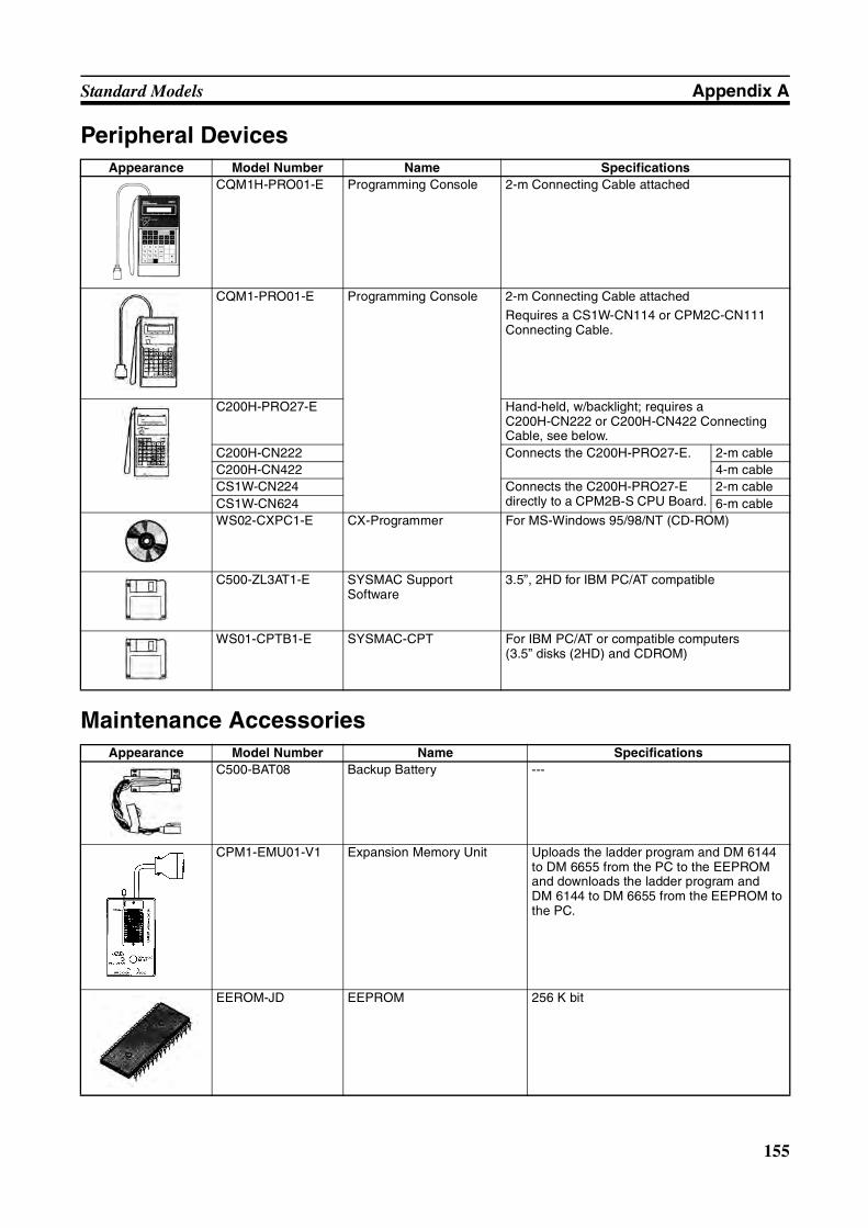
155
Standard Models Appendix A
Peripheral Devices
Maintenance Accessories
Appearance Model Number Name SpecificationsCQM1H-PRO01-E Programming Console 2-m Connecting Cable attached
CQM1-PRO01-E Programming Console 2-m Connecting Cable attached
Requires a CS1W-CN114 or CPM2C-CN111 Connecting Cable.
C200H-PRO27-E Hand-held, w/backlight; requires a C200H-CN222 or C200H-CN422 Connecting Cable, see below.
C200H-CN222 Connects the C200H-PRO27-E. 2-m cableC200H-CN422 4-m cableCS1W-CN224 Connects the C200H-PRO27-E
directly to a CPM2B-S CPU Board.2-m cable
CS1W-CN624 6-m cableWS02-CXPC1-E CX-Programmer For MS-Windows 95/98/NT (CD-ROM)
C500-ZL3AT1-E SYSMAC Support Software
3.5”, 2HD for IBM PC/AT compatible
WS01-CPTB1-E SYSMAC-CPT For IBM PC/AT or compatible computers (3.5” disks (2HD) and CDROM)
Appearance Model Number Name SpecificationsC500-BAT08 Backup Battery ---
CPM1-EMU01-V1 Expansion Memory Unit Uploads the ladder program and DM 6144 to DM 6655 from the PC to the EEPROM and downloads the ladder program and DM 6144 to DM 6655 from the EEPROM to the PC.
EEROM-JD EEPROM 256 K bit
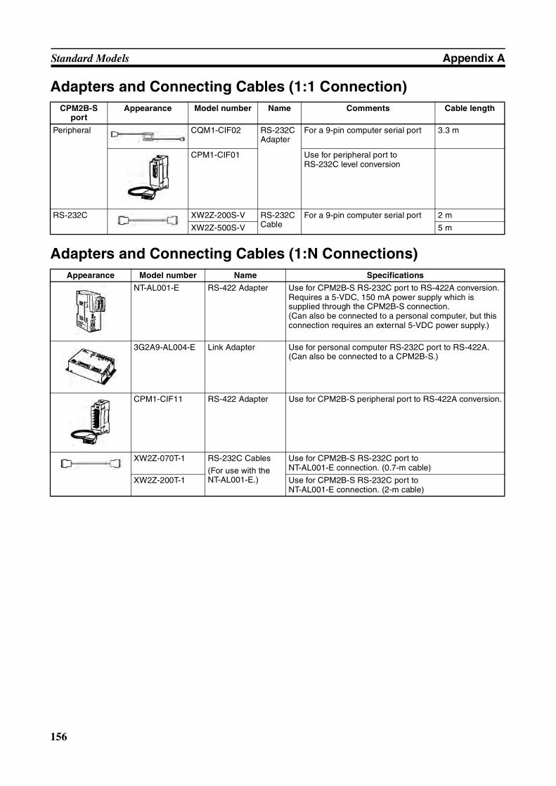
156
Standard Models Appendix A
Adapters and Connecting Cables (1:1 Connection)
Adapters and Connecting Cables (1:N Connections)
CPM2B-S port
Appearance Model number Name Comments Cable length
Peripheral CQM1-CIF02 RS-232C Adapter
For a 9-pin computer serial port 3.3 m
CPM1-CIF01 Use for peripheral port to RS-232C level conversion
RS-232C XW2Z-200S-V RS-232C Cable
For a 9-pin computer serial port 2 m
XW2Z-500S-V 5 m
Appearance Model number Name Specifications
NT-AL001-E RS-422 Adapter Use for CPM2B-S RS-232C port to RS-422A conversion. Requires a 5-VDC, 150 mA power supply which is supplied through the CPM2B-S connection.(Can also be connected to a personal computer, but this connection requires an external 5-VDC power supply.)
3G2A9-AL004-E Link Adapter Use for personal computer RS-232C port to RS-422A.(Can also be connected to a CPM2B-S.)
CPM1-CIF11 RS-422 Adapter Use for CPM2B-S peripheral port to RS-422A conversion.
XW2Z-070T-1 RS-232C Cables
(For use with the NT-AL001-E.)
Use for CPM2B-S RS-232C port to NT-AL001-E connection. (0.7-m cable)
XW2Z-200T-1 Use for CPM2B-S RS-232C port to NT-AL001-E connection. (2-m cable)
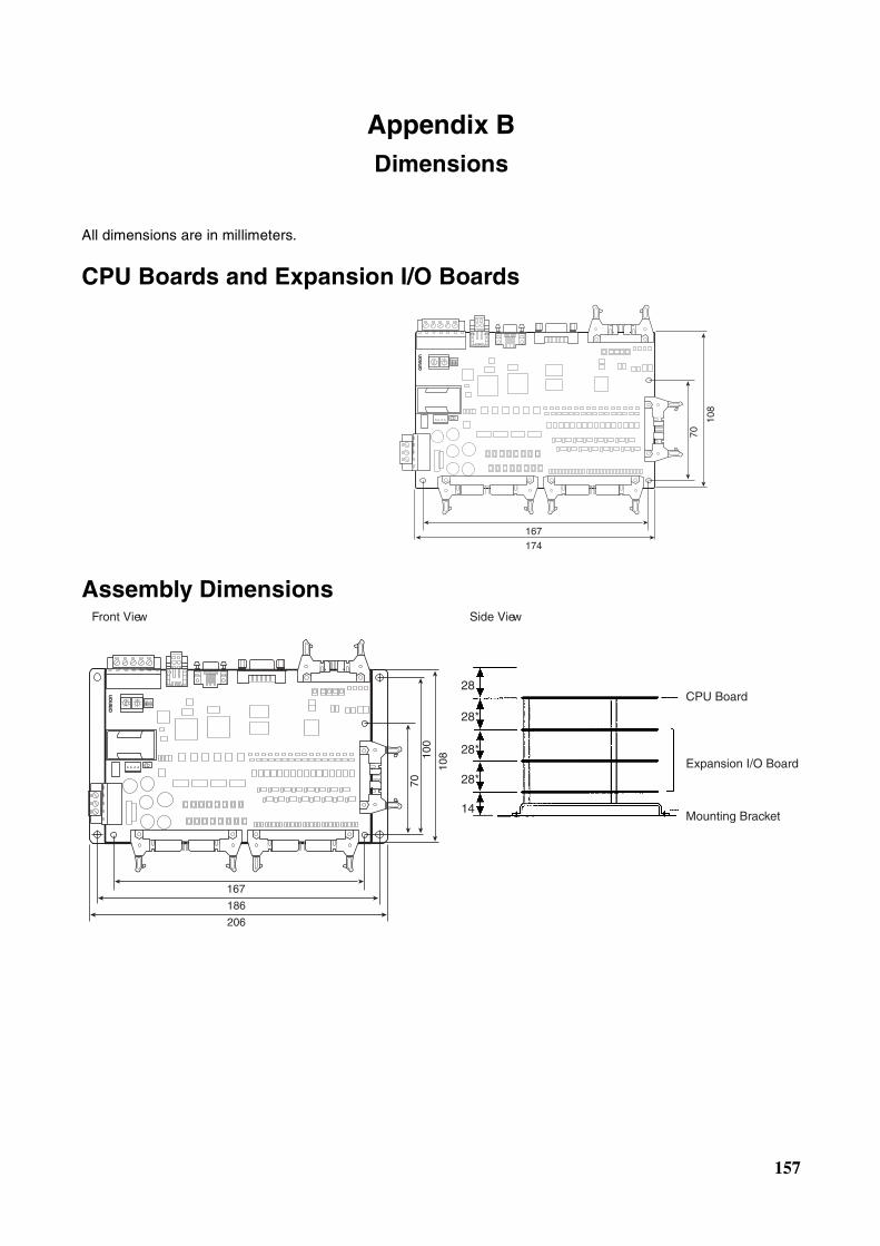
157
Appendix BDimensions
All dimensions are in millimeters.
CPU Boards and Expansion I/O Boards
Assembly Dimensions
174
167
70
108
Front View Side View
CPU Board
Expansion I/O Board
Mounting Bracket
28
28*
28*
28*
14
186
206
167
7010
0
108
159
Index
Numerics1:1 PC Link communications
I/O response timing, 1341:N connections, 11
AAnalog Terminals, 93atmosphere, 22
Bbattery
replacing, 151
Ccabinet
installationprecautions, 35
cablesavailable models, 154, 156
characteristics, 23circuit configuration
inputs, 25communications capabilities
overview, 5Communications Errors, 139communications mode
CompoBus/S communications mode, 92communications speed
DeviceNet Communications, 98communications status
CompoBus/S, 95CompoBus/S communications, 91
communications mode, 92communications status, 95compatible Slaves, 93flags, 95I/O allocation, 94
CompoBus/S Communications Error, 139CompoBus/S Master functions, 91conduit installation, 40CPU Boards
available models, 153dimensions, 157
CPU Unitscyclic operation, 17, 118internal structure, 14
CX-Programmer, 10cycle monitor time
PC Setup settings, 81cycle time (minimum)
PC Setup settings, 82cyclic operation, 17, 118
Ddata link, 6, 13DeviceNet communications, 97
examples, 108
flags, 114LED indicators, 113status information, 113
dielectric strength, 22dimensions, 157duct installation, 39
Eelectrical noise
preventing, 36, 39ERR indicator
flashing, 141lit, 142
error log, 84PC Setup settings, 83
errorserror processing, 137fatal, 142identifying, 139non-fatal, 141user-defined errors, 140
Expansion I/O Boardsavailable models, 153
Expansion I/O Cableavailable models, 153
expansion instructionsfunction codes, 90
explicit message communications, 101
F–HFAL numbers, 141FAL(06), 140FALS numbers, 142FALS(07), 140false inputs, 48fatal errors
troubleshooting, 145features, 2flags
CompoBus/S, 95DeviceNet, 114SR area flags, 66–68
flash memoryprecautions, 138
function codesexpansion instructions, 90
functions, 7hold bit status
PC Setup settings, 80
I–LI/O capacity, 23I/O connectors
available models, 154wiring, 41
I/O errorstroubleshooting, 147
160
Index
I/O line noisepreventing, 39
I/O Modules, 93I/O response time
1:1 PC Link communications, 134See also timing
I/O Terminals, 93indicators
flashing ERR indicator, 141lit ERR indicator, 142PC status indicators, 28
inductive loads, 49–50initialization
time required, 16input devices
connecting, 46input specifications, 25input time constants
PC Setup settings, 82inputs
wiring, 44inrush current
suppressing, 51inspections, 151installation
siteselecting, 35
instructionsexecution times, 121expansion, 90mnemonics list
ladder, 87insulation resistance, 22interlocks, 34interrupt processing
calculating response time, 134masking, 133timing, 133
interrupt program executionin cyclic operation, 19
leakage current, 48LED indicators, 28limit switches
preventing false inputs, 48
Mmaintenance, 151masking
interrupt processes, 133Max. number of CompoBus/S Slaves, 92memory
backup, 24protection, 24
memory areasAR area bits, 69flags and control bits, 66structure, 58
message communications, 101modes
operating modes, 15motor control
capabilities, 4MSG(46), 141
Nnode number
DeviceNet communications, 98noise
preventing electrical noise, 36, 39noise immunity, 22non-fatal errors
troubleshooting, 146NPN current output
connecting, 46NPN open collector
connecting, 46NT Link
connections, 12
Ooperating conditions
troubleshooting, 149operating modes, 15
operating mode at startup, 15output short protection, 50output specifications
transistor outputsink type, 26
Output Terminals, 93
P–Rpanel installation
precautions, 35PC Setup settings, 73PC status
indicators, 28Peripheral Devices, 155
available models, 155peripheral port
servicing time, 81Peripheral Port Error, 140peripheral port servicing time
PC Setup settings, 81photoelectric switches
preventing false inputs, 48PNP current output
connecting, 46position control, 4power
consumption, 22power cables, 39power interruption
detection, 16power supply
Index
161
precautions, 34troubleshooting, 144, 150wiring, 40
precautionsdesign precautions, 34
program capacity, 23program execution
in cyclic operation, 18program write protection
PC Setup settings, 80programming
special features, 90Programming Console
connections, 9proximity switches
preventing false inputs, 48pulse control, 4pulse outputs, 4
wiring, 50quick-response inputs, 4relay outputs
connecting, 46Relay Terminals, 93
connections, 42remote I/O communications
through CompoBus/S, 93through DeviceNet, 98
RS-232C portservicing time, 81
RS-232C Port Error, 139RS-232C port servicing time
PC Setup settings, 81
Sself-diagnosis functions, 24self-diagnostic functions, 139Sensor Amplifier Terminals, 93Sensor Terminals, 93settings
basic operationshold bit status, 80startup mode, 79
I/O operations, 79port servicing scan time, 81–82
shock resistance, 22Slaves
CompoBus/S compatible, 93specifications
characteristics, 23general specifications, 22input specifications, 25output specifications
transistor output, sink type, 26SR area, 66–68startup mode
PC Setup settings, 79Support Software, 10
SYSMAC Support Software, 10SYSMAC-CPT Support Software, 10system
checks, 138system configuration, 8
Ttemperature
operating, storage, 22temperature, ambient, 22terminal blocks
connections, 42test run
procedure, 138timing
basic instructions, 121I/O response time, 131instruction execution
See also instructioninterrupt processing, 133special instructions, 122, 129
troubleshooting, 143fatal errors, 145I/O errors, 147non-fatal errors, 146operating conditions, 149power supply, 144, 150
U–Wvibration resistance, 22voltage
supply voltage, 22voltage output
connecting, 46wiring, 39
I/O connectors, 41power supply, 40
write protecting the programPC Setup settings, 80
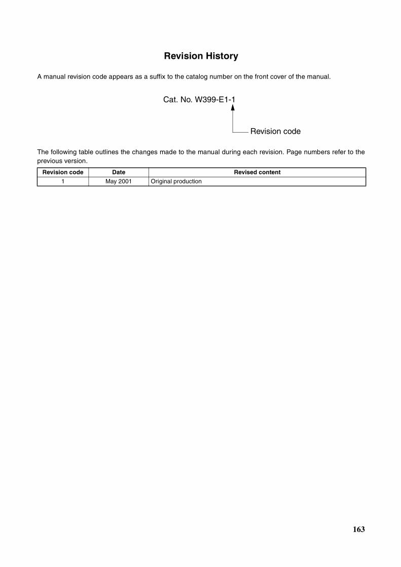
163
Revision History
A manual revision code appears as a suffix to the catalog number on the front cover of the manual.
The following table outlines the changes made to the manual during each revision. Page numbers refer to theprevious version.
Revision code Date Revised content
1 May 2001 Original production
Cat. No. W399-E1-1
Revision code