Embed Size (px)
Citation preview

System Cache v3.1
LogiCORE IP Product Guide
Vivado Design Suite
PG118 November 18, 2015
System Cache v3.1 www.xilinx.com 2PG118 November 18, 2015
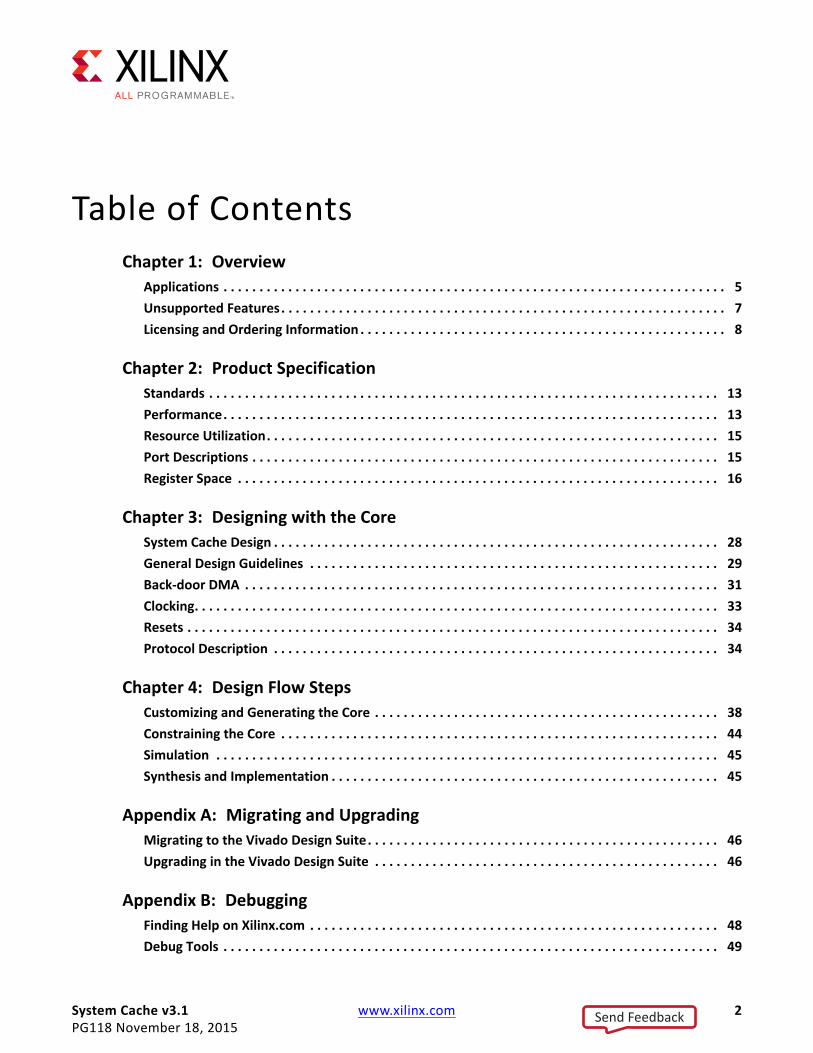
Table of ContentsChapter 1: Overview
Applications . . . . . . . . . . . . . . . . . . . . . . . . . . . . . . . . . . . . . . . . . . . . . . . . . . . . . . . . . . . . . . . . . . . . . . 5Unsupported Features. . . . . . . . . . . . . . . . . . . . . . . . . . . . . . . . . . . . . . . . . . . . . . . . . . . . . . . . . . . . . . 7Licensing and Ordering Information . . . . . . . . . . . . . . . . . . . . . . . . . . . . . . . . . . . . . . . . . . . . . . . . . . . 8
Chapter 2: Product SpecificationStandards . . . . . . . . . . . . . . . . . . . . . . . . . . . . . . . . . . . . . . . . . . . . . . . . . . . . . . . . . . . . . . . . . . . . . . . 13Performance. . . . . . . . . . . . . . . . . . . . . . . . . . . . . . . . . . . . . . . . . . . . . . . . . . . . . . . . . . . . . . . . . . . . . 13Resource Utilization. . . . . . . . . . . . . . . . . . . . . . . . . . . . . . . . . . . . . . . . . . . . . . . . . . . . . . . . . . . . . . . 15Port Descriptions . . . . . . . . . . . . . . . . . . . . . . . . . . . . . . . . . . . . . . . . . . . . . . . . . . . . . . . . . . . . . . . . . 15Register Space . . . . . . . . . . . . . . . . . . . . . . . . . . . . . . . . . . . . . . . . . . . . . . . . . . . . . . . . . . . . . . . . . . . 16
Chapter 3: Designing with the CoreSystem Cache Design . . . . . . . . . . . . . . . . . . . . . . . . . . . . . . . . . . . . . . . . . . . . . . . . . . . . . . . . . . . . . . 28General Design Guidelines . . . . . . . . . . . . . . . . . . . . . . . . . . . . . . . . . . . . . . . . . . . . . . . . . . . . . . . . . 29Back-door DMA . . . . . . . . . . . . . . . . . . . . . . . . . . . . . . . . . . . . . . . . . . . . . . . . . . . . . . . . . . . . . . . . . . 31Clocking. . . . . . . . . . . . . . . . . . . . . . . . . . . . . . . . . . . . . . . . . . . . . . . . . . . . . . . . . . . . . . . . . . . . . . . . . 33Resets . . . . . . . . . . . . . . . . . . . . . . . . . . . . . . . . . . . . . . . . . . . . . . . . . . . . . . . . . . . . . . . . . . . . . . . . . . 34Protocol Description . . . . . . . . . . . . . . . . . . . . . . . . . . . . . . . . . . . . . . . . . . . . . . . . . . . . . . . . . . . . . . 34
Chapter 4: Design Flow StepsCustomizing and Generating the Core . . . . . . . . . . . . . . . . . . . . . . . . . . . . . . . . . . . . . . . . . . . . . . . . 38Constraining the Core . . . . . . . . . . . . . . . . . . . . . . . . . . . . . . . . . . . . . . . . . . . . . . . . . . . . . . . . . . . . . 44Simulation . . . . . . . . . . . . . . . . . . . . . . . . . . . . . . . . . . . . . . . . . . . . . . . . . . . . . . . . . . . . . . . . . . . . . . 45Synthesis and Implementation . . . . . . . . . . . . . . . . . . . . . . . . . . . . . . . . . . . . . . . . . . . . . . . . . . . . . . 45
Appendix A: Migrating and UpgradingMigrating to the Vivado Design Suite. . . . . . . . . . . . . . . . . . . . . . . . . . . . . . . . . . . . . . . . . . . . . . . . . 46Upgrading in the Vivado Design Suite . . . . . . . . . . . . . . . . . . . . . . . . . . . . . . . . . . . . . . . . . . . . . . . . 46
Appendix B: DebuggingFinding Help on Xilinx.com . . . . . . . . . . . . . . . . . . . . . . . . . . . . . . . . . . . . . . . . . . . . . . . . . . . . . . . . . 48Debug Tools . . . . . . . . . . . . . . . . . . . . . . . . . . . . . . . . . . . . . . . . . . . . . . . . . . . . . . . . . . . . . . . . . . . . . 49
Send Feedback

System Cache v3.1 www.xilinx.com 3PG118 November 18, 2015
Simulation Debug. . . . . . . . . . . . . . . . . . . . . . . . . . . . . . . . . . . . . . . . . . . . . . . . . . . . . . . . . . . . . . . . . 50Hardware Debug . . . . . . . . . . . . . . . . . . . . . . . . . . . . . . . . . . . . . . . . . . . . . . . . . . . . . . . . . . . . . . . . . 50Interface Debug . . . . . . . . . . . . . . . . . . . . . . . . . . . . . . . . . . . . . . . . . . . . . . . . . . . . . . . . . . . . . . . . . . 51
Appendix C: Additional Resources and Legal NoticesXilinx Resources . . . . . . . . . . . . . . . . . . . . . . . . . . . . . . . . . . . . . . . . . . . . . . . . . . . . . . . . . . . . . . . . . . 53References . . . . . . . . . . . . . . . . . . . . . . . . . . . . . . . . . . . . . . . . . . . . . . . . . . . . . . . . . . . . . . . . . . . . . . 53Revision History . . . . . . . . . . . . . . . . . . . . . . . . . . . . . . . . . . . . . . . . . . . . . . . . . . . . . . . . . . . . . . . . . . 54Please Read: Important Legal Notices . . . . . . . . . . . . . . . . . . . . . . . . . . . . . . . . . . . . . . . . . . . . . . . . 54
Send Feedback
System Cache v3.1 www.xilinx.com 4PG118 November 18, 2015 Product Specification
IntroductionThe LogiCORE™ System Cache IP core provides system level caching capability to an AMBA® AXI4 system. The System Cache core resides in front of the external memory controller and is seen as a Level 2 cache from the MicroBlaze™ processor point of view.
Features• Dedicated AXI4 slave ports for MicroBlaze
• Connects up to 16 MicroBlaze cache ports, normally eight processors
• Up to 16 generic AXI4 slave ports for other AXI4 masters
• Optional cache coherency on dedicated MicroBlaze ports with AXI Coherency Extension (ACE)
• Optional support for exclusive access with non-coherent configuration
• AXI4 master port connecting the external memory controller
• Highly configurable cache
• Optional AXI4-Lite Statistics and Control port
• Supports up to 64 bit AXI4 address width
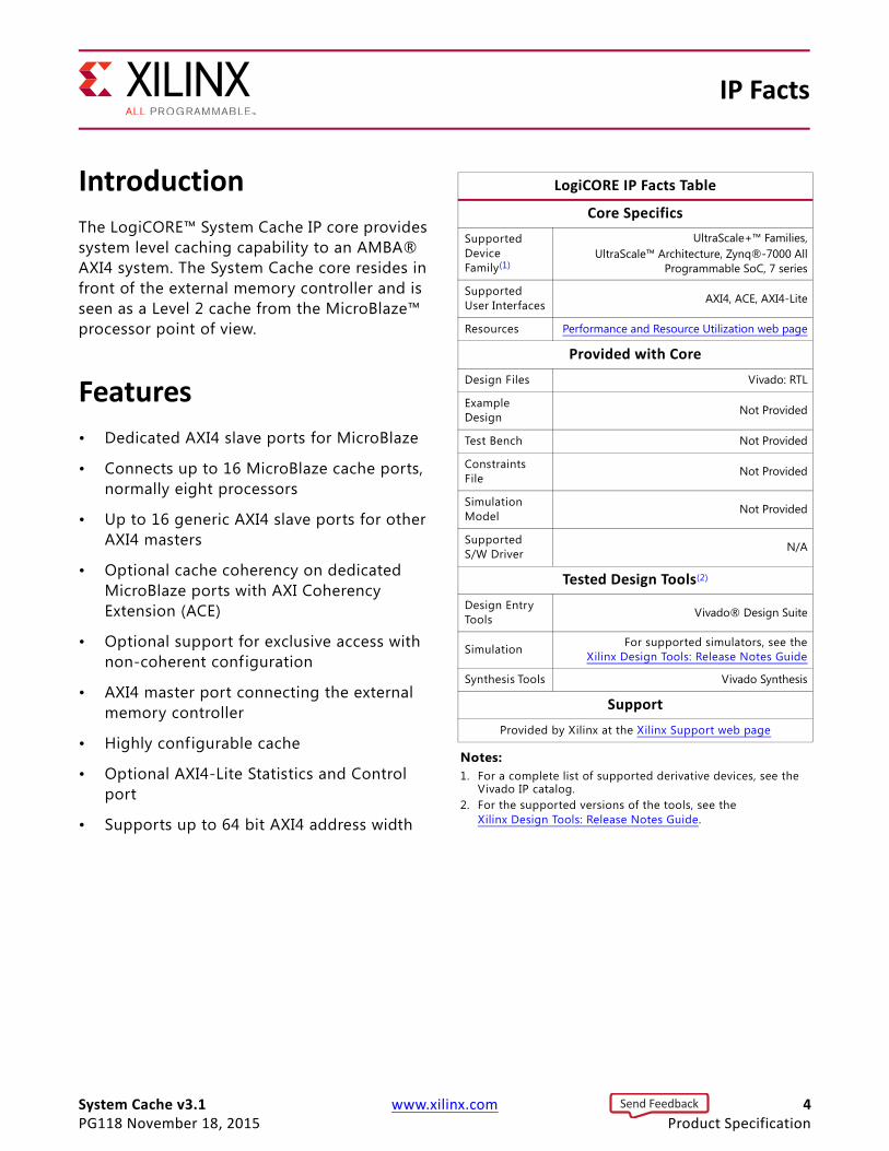
IP Facts
LogiCORE IP Facts Table
Core SpecificsSupported Device Family(1)
UltraScale+™ Families, UltraScale™ Architecture, Zynq®-7000 All
Programmable SoC, 7 series
Supported User Interfaces AXI4, ACE, AXI4-Lite
Resources Performance and Resource Utilization web page
Provided with CoreDesign Files Vivado: RTL
Example Design Not Provided
Test Bench Not Provided
Constraints File Not Provided
Simulation Model Not Provided
Supported S/W Driver N/A
Tested Design Tools(2)
Design Entry Tools Vivado® Design Suite
Simulation For supported simulators, see theXilinx Design Tools: Release Notes Guide
Synthesis Tools Vivado Synthesis
SupportProvided by Xilinx at the Xilinx Support web page
Notes: 1. For a complete list of supported derivative devices, see the
Vivado IP catalog.2. For the supported versions of the tools, see the
Xilinx Design Tools: Release Notes Guide.
Send Feedback
System Cache v3.1 www.xilinx.com 5PG118 November 18, 2015
Chapter 1
OverviewThe System Cache IP core can be added to an AXI4 system to improve overall system computing performance, for accesses to external memory. The System Cache core is typically used in a MicroBlaze™ system implementing a Level 2 cache with up to eight MicroBlaze processors. The generic AXI4 interface provides access to the caching capability of all other AXI4 masters in the system.
With cache coherency, eff icient multi-processor systems can be implemented and the workload distributed between multiple processors, with simple and safe data sharing. The coherency is managed on a hardware level with minimal software handling required.
The System Cache core can provide improved system performance for:
• Applications with repeated access of data occupying a certain address range, for example, when external memory is used to buffer data during computations. In particular, performance improvements are achieved when the data set exceeds the capacity of the MicroBlaze internal data cache.
• Systems with small MicroBlaze caches, for example, when the MicroBlaze implementation is tuned to achieve as high frequency as possible. In this case, the increased system frequency contributes to the performance improvements, and the System Cache core alleviates the performance loss incurred by the reduced size of the MicroBlaze internal caches.
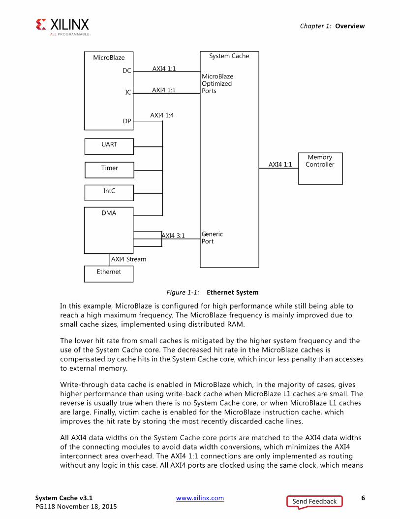
ApplicationsAn example of an Ethernet communication system is given in Figure 1-1. The system consists of a MicroBlaze processor connected point-to-point to two optimized ports of the System Cache core. A DMA controller is connected to a Generic port on the System Cache core through a 3:1 AXI4 interconnect, because the DMA controller has three AXI4 master ports. The DMA in turn is connected to the Ethernet IP by AXI4-Stream links. Standard peripheral functions like UART, timer, interrupt controller as well as the DMA controller control port are connected to the MicroBlaze peripheral data port (M_AXI_DP) for register configuration and control.
With this partitioning the bandwidth critical interfaces are connected directly to the System Cache core and kept completely separated from the AXI4-Lite based configuration and control connections. This system is used as an example throughout the documentation.
Send Feedback
System Cache v3.1 www.xilinx.com 6PG118 November 18, 2015
Chapter 1: Overview
In this example, MicroBlaze is configured for high performance while still being able to reach a high maximum frequency. The MicroBlaze frequency is mainly improved due to small cache sizes, implemented using distributed RAM.
The lower hit rate from small caches is mitigated by the higher system frequency and the use of the System Cache core. The decreased hit rate in the MicroBlaze caches is compensated by cache hits in the System Cache core, which incur less penalty than accesses to external memory.
Write-through data cache is enabled in MicroBlaze which, in the majority of cases, gives higher performance than using write-back cache when MicroBlaze L1 caches are small. The reverse is usually true when there is no System Cache core, or when MicroBlaze L1 caches are large. Finally, victim cache is enabled for the MicroBlaze instruction cache, which improves the hit rate by storing the most recently discarded cache lines.
All AXI4 data widths on the System Cache core ports are matched to the AXI4 data widths of the connecting modules to avoid data width conversions, which minimizes the AXI4 interconnect area overhead. The AXI4 1:1 connections are only implemented as routing without any logic in this case. All AXI4 ports are clocked using the same clock, which means
X-Ref Target - Figure 1-1
Figure 1-1: Ethernet System
MemoryController
System Cache
DMA
MicroBlaze
DC
IC
DP
UART
Timer
IntC
Ethernet
AXI4 1:1
AXI4 1:1
AXI4 1:1
AXI4 3:1
AXI4 1:4
AXI4 Stream
MicroBlazeOptimizedPorts
GenericPort
Send Feedback

System Cache v3.1 www.xilinx.com 7PG118 November 18, 2015
Chapter 1: Overview
that there is no need for clock conversion within the AXI4 interconnects. Avoiding clock conversion gives minimal area and latency for the AXI4 interconnects. The parameter settings for MicroBlaze and the System Cache core can be found in Table 1-1 and Table 1-2, respectively.
Unsupported Features
Non Coherent ImplementationThe System Cache core provides no support for coherency between the MicroBlaze internal caches when the cache coherency is disabled. This means that software must ensure coherency for data exchanged between the processors. When the MicroBlaze processors use write-back data caches, all processors need to flush their caches to ensure that correct data is being exchanged. For write-through caches, it is only the processors reading data that need to flush their caches to ensure that correct data is being exchanged.
Table 1-1: MicroBlaze Parameter Settings for the Ethernet System
Parameter Value
C_CACHE_BYTE_SIZE 512
C_ICACHE_ALWAYS_USED 1
C_ICACHE_LINE_LEN 8
C_ICACHE_STREAMS 0
C_ICACHE_VICTIMS 8
C_DCACHE_BYTE_SIZE 512
C_DCACHE_ALWAYS_USED 1
C_DCACHE_LINE_LEN 8
C_DCACHE_USE_WRITEBACK 0
C_DCACHE_VICTIMS 0
Table 1-2: System Cache Parameter Settings for the Ethernet System
Parameter Value
C_NUM_OPTIMIZED_PORTS 2
C_NUM_GENERIC_PORTS 1
C_NUM_SETS 4
C_CACHE_SIZE 65536
C_M_AXI_DATA_WIDTH 32
Send Feedback

System Cache v3.1 www.xilinx.com 8PG118 November 18, 2015
Chapter 1: Overview
Cache Coherent ImplementationWhen cache coherency is enabled masters connected through the Generic AXI4 slave ports are not included in the coherency domain, but their accesses are monitored by the coherency domain, such that data remains coherent within the domain (that is, read accesses by these AXI4 masters read the correct value, and write accesses update the value within the coherency domain). Coherency is not ensured for any cached or local data outside this domain.
Exclusive transactions from the Generic ports are disabled, and treated as normal transaction, when cache coherency is enabled. This is because only the ACE transaction based method with snoop messages is supported with cache coherency enabled.
The secure/non-secure bit in AxPROT is not used to expand the memory address range. Both types are treated equally.
Licensing and Ordering InformationThis Xilinx LogiCORE™ IP module is provided at no additional cost with the Xilinx Vivado® Design Suite under the terms of the Xilinx End User License. Information about this and other Xilinx LogiCORE IP modules is available at the Xilinx Intellectual Property page. For information on pricing and availability of other Xilinx LogiCORE IP modules and tools, contact your local Xilinx sales representative.
Send Feedback

System Cache v3.1 www.xilinx.com 9PG118 November 18, 2015
Chapter 2
Product SpecificationIn a typical system with one MicroBlaze processor, as shown in Figure 2-1 and Figure 2-2, the instruction and data cache interfaces (M_AXI_IC and M_AXI_DC) are connected to dedicated AXI4 interfaces optimized for MicroBlaze on the System Cache core. The System Cache core often makes it possible to reduce the MicroBlaze internal cache sizes, without reducing system performance. Non-MicroBlaze AXI4 interface masters are connected to one or more of the generic AXI4 slave interfaces of the System Cache core either directly (Figure 2-2) or through an AXI4 interconnect (Figure 2-1).
The System Cache core can also be used in a system without any MicroBlaze processor, as shown in Figure 2-3. For this case, it is also possible to have multiple Generic ports.
X-Ref Target - Figure 2-1
Figure 2-1: Typical System With a Single ProcessorX-Ref Target - Figure 2-2
Figure 2-2: Typical System With a Single Processor
MemoryController
SystemCache
AXI4Interconnect
MicroBlaze
M_AXI_DC
M_AXI_IC
MemoryController
SystemCache
MicroBlaze
M_AXI_DC
M_AXI_IC
Send Feedback

System Cache v3.1 www.xilinx.com 10PG118 November 18, 2015
Chapter 2: Product Specification
The System Cache core has 16 cache interfaces optimized for MicroBlaze, enabling direct connection of up to eight MicroBlaze processors, as shown in Figure 2-4.
The 16 cache interfaces optimized for MicroBlaze provide support for up to eight cache coherent MicroBlaze processors, as shown in Figure 2-5.
X-Ref Target - Figure 2-3
Figure 2-3: System Without Processor
X-Ref Target - Figure 2-4
Figure 2-4: Typical System With Multiple MicroBlaze Processors
MemoryController
SystemCache
AXI4Interconnect
MemoryController
SystemCache
AXI4Interconnect
MicroBlaze
MicroBlaze
M_AXI_DC
M_AXI_IC
M_AXI_DC
M_AXI_IC
Send Feedback

System Cache v3.1 www.xilinx.com 11PG118 November 18, 2015
Chapter 2: Product Specification
Cache CoherencyCache coherency support is used to enable data and instruction cache coherency for multiple MicroBlaze cores. It provides reliable exclusive transactions to implement software spinlocks and simplif ies multi-processor (MP) systems where data is shared among the processors. Any data that is updated from one MicroBlaze is guaranteed to be seen from its peer processors without any special software interactions other than ordinary single MicroBlaze rules for handling self-modifying code. This data manipulation information exchange is handled by the snooping mechanism provided by the AXI Coherency Extension (ACE) (see the AMBA AXI and ACE Protocol Specification [Ref 1]). DVM, Distributed Virtual Memory, messages are also available with ACE to ensure that MMU and Branch Target Caches are updated across the system when related changes are performed by any of the connected processors.
Exclusive MonitorThe optional exclusive monitor provide full support for exclusive transactions when cache coherency is disabled. It supports exclusive transactions from both Generic and Optimized ports.
Cache MemoryThe cache memory provides the actual cache functionality in the core. The cache is configurable in terms of size and associativity.
X-Ref Target - Figure 2-5
Figure 2-5: Typical System With Multiple Coherent MicroBlaze Processors
MemoryController
SystemCache
AXI4Interconnect
MicroBlaze
MicroBlaze
M_ACE_DC
M_ACE_IC
M_ACE_DC
M_ACE_IC
Send Feedback

System Cache v3.1 www.xilinx.com 12PG118 November 18, 2015
Chapter 2: Product Specification
The cache size can be configured with the parameter C_CACHE_SIZE according to Table 4-1. The selected size is a trade-off between performance and resource usage, in particular the number of block RAMs.
The associativity can be configured with the parameter C_NUM_SETS according to Table 4-1. Increased associativity generally provides better hit rate, which gives better performance but requires more area resources.
The correspondence between selected parameters and block RAMs used can be found in Performance and Resource Utilization.
Statistics and ControlThe optional Statistics and Control block can be used to collect cache statistics such as cache hit rate and access latency. The statistics are primarily intended for internal Xilinx use, but can also be used to tailor the configuration of the System Cache core to meet the needs of a specif ic application.
The following types of statistics are collected:
• Port statistics for each slave interface
° Total Read and Write transaction counts
° Port queue usage for the six transaction queues associated with each port
° Cache hit rates for read and write
° Read and Write transaction latency
• Arbitration statistics
• Functional unit statistics
° Stall cycles
° Internal queue usage
• Port statistics for the master interface
° Read and write latency
The following types of control and configuration information are available:
• Control registers for Flush and Clear cache maintenance
• Version Registers with System Cache core configuration
For details on the registers used to read statistics and control how statistics is gathered, see Register Space.
Send Feedback

System Cache v3.1 www.xilinx.com 13PG118 November 18, 2015
Chapter 2: Product Specification
StandardsThe System Core adheres to the AMBA® AXI4 Interface standard (see ARM® AMBA AXI Protocol Specification, Version 2.0 ARM IHI 0022E [Ref 1]).
PerformanceThe perceived performance is dependent on many factors such as frequency, latency and throughput. Which factor has the dominating effect is application-specific. There is also a correlation between the performance factors; for example, achieving high frequency can add latency and also wide datapaths for throughput can adversely affect frequency.
Maximum FrequenciesFor details about performance, visit Performance and Resource Utilization.
Cache LatencyRead latency is defined as the clock cycle from the read address is accepted by the System Cache core to the cycle when f irst read data is available.
Write latency is defined as the clock cycle from the write address is accepted by the System Cache core to the cycle when the BRESP is valid. These calculations assume that the start of the write data is aligned to the transaction address.
The latency depends on many factors such as traff ic from other ports and conflict with earlier transactions. The numbers in Table 2-1 assume a completely idle System Cache core and no write data delay for transactions on one of the Optimized ports. For transactions using a Generic AXI4 port an additional two clock cycle latency is added.
Table 2-1: System Cache Latencies for Optimized Port
Type Optimized Port Latency
Read Hit 5
Read Miss 6 + latency added by memory subsystem
Read Miss DirtyMaximum of:6 + latency added by memory subsystem6 + latency added for evicting dirty data (cache line length * 32 / M_AXI Data Width)
Write Hit 2 + burst length
Write Miss Non-bufferable transaction: 6 + latency added by memory subsystem for writing dataBufferable transaction: Same as Write Hit
Send Feedback

System Cache v3.1 www.xilinx.com 14PG118 November 18, 2015
Chapter 2: Product Specification
Enabling cache coherency affects the latency and also introduces new types of transaction latencies. The numbers in Table 2-2 assume a completely idle System Cache core and no write data delay for transactions on one of the Optimized ports. Transactions from a Generic port still have two cycles of extra latency.
The numbers for an actual application vary depending on access patterns, hit/miss ratio and other factors. Example values from a system (see Figure 2-1) running the iperf network testing tool with the LWIP TCP/IP stack in raw mode are shown in Tables 2-3 to 2-6. Table 2-3 contains the hit rate for transactions from all ports. Table 2-4, Table 2-5 and Table 2-6 show per port hit rate and latencies for the three active ports.
Table 2-2: System Cache Latencies for Cache Coherent Optimized Port
Type Coherent Optimized Port Latency
DVM Message 8 + latency added by snooped masters
DVM Sync 11 + latency added by snooped masters
Read Hit 8 + latency added by snooped masters
Read Miss 9 + latency added by snooped masters + latency added by memory subsystem
Read Miss Dirty
Maximum of:9 + latency added by snooped masters + latency added by memory subsystem9 + latency added by snooped masters + latency added for evicting dirty data (cache line length * 32 / M_AXI Data Width)
Write HitMaximum of:2 + burst length5 + latency added by snooped masters
Write MissNon-bufferable transaction: 9 + latency added by snooped masters + latency added by memory subsystem for writing dataBufferable transaction: same as Write Hit
Table 2-3: Application Total Hit Rates
Type Hit Rate
Read 99.82%
Write 92.93%
Table 2-4: System Cache Hit Rate and Latencies for MicroBlaze D-Side Port
Type Hit Rate Min Max Average Standard Deviation
Read 99.68% 5 289 7 3
Write 96.63% 3 30 3 1
Table 2-5: System Cache Hit Rate and Latencies for MicroBlaze I-Side Port
Type Hit Rate Min Max Average Standard Deviation
Read 9.96% 5 568 6 2
Write N/A N/A N/A N/A N/A
Send Feedback

System Cache v3.1 www.xilinx.com 15PG118 November 18, 2015
Chapter 2: Product Specification
ThroughputThe System Cache core is fully pipelined and can have a theoretical maximum transaction rate of one read or write hit data concurrent with one read and one write miss data per clock cycle when there are no conflicts with earlier transactions.
This theoretical limit is subject to memory subsystem bandwidth, intra-transaction conflicts and cache hit detection overhead, which reduce the achieved throughput to less than three data beats per clock cycle.
Resource UtilizationFor details about resource utilization, visit Performance and Resource Utilization.
Port DescriptionsThe block diagram for the System Cache core is shown in Figure 2-6. All System Cache core interfaces are compliant with AXI4. The input signals ACLK and ARESETN implement clock and reset for the entire System Cache core.
Table 2-6: System Cache Hit Rate and Latencies for Generic Port
Type Hit Rate Min Max Average Standard Deviation
Read 76.68% 7 388 18 13
Write 9.78% 6 112 24 5
X-Ref Target - Figure 2-6
Figure 2-6: System Cache Block Diagram
MemoryControllerInterface
CacheMicroBlazeCache Ports
#0...
#15Arbiter
+Coherency
System CacheAXI4 Slave
Ports
AXI4 MasterPort
Control Port
ACLKARESETN
Statistics+
Control
GenericPorts
#0...
#15
Send Feedback

System Cache v3.1 www.xilinx.com 16PG118 November 18, 2015
Chapter 2: Product Specification
Register SpaceAll registers in the optional Statistics module are 64 bits wide. The address map structure is shown in Table 2-8.
The address coding of all functional units in the System Cache core with statistics gathering capability is defined in Table 2-9.
Table 2-7: System Cache I/O Interfaces
Interface Name Type Description
ACLK Input Clock for System Cache
ARESETN Input Synchronous reset of System Cache
Sx_AXI(1)(2) AXI4 Slave MicroBlaze Optimized Cache port
Sx_ACE(1)(2) ACE Slave MicroBlaze Optimized Cache Coherent port
Sx_AXI_GEN(1) AXI4 Slave Generic Cache Port
M_AXI AXI4 Master Memory Controller Master port
S_AXI_CTRL AX4-lite Slave Control port
Notes: 1. x = 0–152. Mutually exclusive
Table 2-8: Address Structure
Category Port Number Functionality Register High/Low
Always 00
16 14 13 10 9 5 4 3 2 1 0
Send Feedback

System Cache v3.1 www.xilinx.com 17PG118 November 18, 2015
Chapter 2: Product Specification
Table 2-9: System Cache Address Map, Category and Port Number Field
Address (binary) Category and Port number Description
0_0000_00xx_xxxx_xx00 Optimized port 0
All statistics for the Optimized ports are defined in Table 2-10 when used, 0 otherwise.
0_0000_01xx_xxxx_xx00 Optimized port 1
0_0000_10xx_xxxx_xx00 Optimized port 2
0_0000_11xx_xxxx_xx00 Optimized port 3
0_0001_00xx_xxxx_xx00 Optimized port 4
0_0001_01xx_xxxx_xx00 Optimized port 5
0_0001_10xx_xxxx_xx00 Optimized port 6
0_0001_11xx_xxxx_xx00 Optimized port 7
0_0010_00xx_xxxx_xx00 Optimized port 8
0_0010_01xx_xxxx_xx00 Optimized port 9
0_0010_10xx_xxxx_xx00 Optimized port 10
0_0010_11xx_xxxx_xx00 Optimized port 11
0_0011_00xx_xxxx_xx00 Optimized port 12
0_0011_01xx_xxxx_xx00 Optimized port 13
0_0011_10xx_xxxx_xx00 Optimized port 14
0_0011_11xx_xxxx_xx00 Optimized port 15
0_0100_00xx_xxxx_xx00 Generic port 0
All statistics for the Generic ports are defined in Table 2-11 when used, 0 otherwise.
0_0100_01xx_xxxx_xx00 Generic port 1
0_0100_10xx_xxxx_xx00 Generic port 2
0_0100_11xx_xxxx_xx00 Generic port 3
0_0101_00xx_xxxx_xx00 Generic port 4
0_0101_01xx_xxxx_xx00 Generic port 5
0_0101_10xx_xxxx_xx00 Generic port 6
0_0101_11xx_xxxx_xx00 Generic port 7
0_0110_00xx_xxxx_xx00 Generic port 8
0_0110_01xx_xxxx_xx00 Generic port 9
0_0110_10xx_xxxx_xx00 Generic port 10
0_0110_11xx_xxxx_xx00 Generic port 11
0_0111_00xx_xxxx_xx00 Generic port 12
0_0111_01xx_xxxx_xx00 Generic port 13
0_0111_10xx_xxxx_xx00 Generic port 14
0_0111_11xx_xxxx_xx00 Generic port 15
0_1000_00xx_xxxx_xx00 Arbiter Statistics available in arbiter stage defined in Table 2-12
0_1100_00xx_xxxx_xx00 Access Statistics available in access stage defined in Table 2-13
1_0000_00xx_xxxx_xx00 Lookup Statistics available in lookup stage defined in Table 2-14
1_0100_00xx_xxxx_xx00 Update Statistics available in update stage defined in Table 2-15
1_1000_00xx_xxxx_xx00 Backend Statistics available in backend stage defined in Table 2-16
1_1100_00xx_xxxx_xx00 Control Control registers defined in Table 2-17
Send Feedback

System Cache v3.1 www.xilinx.com 18PG118 November 18, 2015
Chapter 2: Product Specification
Table 2-10 shows the address decoding for the statistics functionality in the Optimized ports.
Table 2-10: System Cache Address Map, Statistics Field for Optimized Port
Address (binary) Functionality R/W StatisticsFormat Description
0_00yy_yy00_000x_xx00 Read Segments R COUNT(1) Number of segments per read transaction
0_00yy_yy00_001x_xx00 Write Segments R COUNT(1) Number of segments per write transaction
0_00yy_yy00_010x_xx00 RIP R QUEUE(2) Read Information Port queue statistics
0_00yy_yy00_011x_xx00 R R QUEUE(2) Read data queue statistics
0_00yy_yy00_100x_xx00 BIP R QUEUE(2) BRESP Information Port queue statistics
0_00yy_yy00_101x_xx00 BP R QUEUE(2) BRESP Port queue statistics
0_00yy_yy00_110x_xx00 WIP R QUEUE(2) Write Information Port queue statistics
0_00yy_yy00_111x_xx00 W R QUEUE(2) Write data queue statistics
0_00yy_yy01_000x_xx00 Read Blocked R COUNT(1)Number of cycles a read was prohibited from taking part in arbitration
0_00yy_yy01_001x_xx00 Write Hit R COUNT(1) Number of write hits
0_00yy_yy01_010x_xx00 Write Miss R COUNT(1) Number of write misses
0_00yy_yy01_011x_xx00 Write Miss Dirty R COUNT(1) Number of dirty write misses
0_00yy_yy01_100x_xx00 Read Hit R COUNT(1) Number of read hits
0_00yy_yy01_101x_xx00 Read Miss R COUNT(1) Number of read misses
0_00yy_yy01_110x_xx00 Read Miss Dirty R COUNT(1) Number of dirty read misses
0_00yy_yy01_111x_xx00 Locked Write Hit R COUNT(1) Number of locked write hits
0_00yy_yy10_000x_xx00 Locked Read Hit R COUNT(1) Number of locked read hits
0_00yy_yy10_001x_xx00 First Write Hit R COUNT(1) Number of f irst write hits
0_00yy_yy10_010x_xx00 Read Latency R COUNT(1) Read latency statistics
0_00yy_yy10_011x_xx00 Write Latency R COUNT(1) Write latency statistics
0_00yy_yy10_100x_xx00 Read LatencyConfiguration R/W LONGINT(3)
Configuration for read latency statistics collection. Default value 0. Available modes are defined in Table 2-25.
0_00yy_yy10_101x_xx00 Write LatencyConfiguration R/W LONGINT(3)
Configuration for read latency statistics collection. Default value 4. Available modes are defined in Table 2-26.
Notes: 1. See Table 2-18 for the COUNT register f ields2. See Table 2-19 for the QUEUE register fields.3. See Table 2-20 for the LONGINT register f ields.
Send Feedback

System Cache v3.1 www.xilinx.com 19PG118 November 18, 2015
Chapter 2: Product Specification
Table 2-11 shows the address decoding for the statistics functionality in the Generic ports.
Table 2-11: System Cache Address Map, Statistics Field for Generic Port
Address (binary) Functionality R/W Statistics Format Description
0_01yy_yy00_000x_xx00 Read Segments R COUNT(1) Number of segments per read transaction
0_01yy_yy00_001x_xx00 Write Segments R COUNT(1) Number of segments per write transaction
0_01yy_yy00_010x_xx00 RIP R QUEUE(2) Read Information Port queue statistics
0_01yy_yy00_011x_xx00 R R QUEUE(2) Read data queue statistics
0_01yy_yy00_100x_xx00 BIP R QUEUE(2) BRESP Information Port queue statistics
0_01yy_yy00_101x_xx00 BP R QUEUE(2) BRESP Port queue statistics
0_01yy_yy00_110x_xx00 WIP R QUEUE(2) Write Information Port queue statistics
0_01yy_yy00_111x_xx00 W R QUEUE(2) Write data queue statistics
0_01yy_yy01_000x_xx00 Read Blocked R COUNT(1)Number of cycles a read was prohibited from taking part in arbitration
0_01yy_yy01_001x_xx00 Write Hit R COUNT(1) Number of write hits
0_01yy_yy01_010x_xx00 Write Miss R COUNT(1) Number of write misses
0_01yy_yy01_011x_xx00 Write Miss Dirty R COUNT(1) Number of dirty write misses
0_01yy_yy01_100x_xx00 Read Hit R COUNT(1) Number of read hits
0_01yy_yy01_101x_xx00 Read Miss R COUNT(1) Number of read misses
0_01yy_yy01_110x_xx00 Read Miss Dirty R COUNT(1) Number of dirty read misses
0_01yy_yy01_111x_xx00 Locked Write Hit R COUNT(1) Number of locked write hits
0_01yy_yy10_000x_xx00 Locked Read Hit R COUNT(1) Number of locked read hits
0_01yy_yy10_001x_xx00 First Write Hit R COUNT(1) Number of f irst write hits
0_01yy_yy10_010x_xx00 Read Latency R COUNT(1) Read latency statistics
0_01yy_yy10_011x_xx00 Write Latency R COUNT(1) Write latency statistics
0_01yy_yy10_100x_xx00 Read LatencyConfiguration R/W LONGINT(3)
Configuration for read latency statistics collection. Default value 0. Modes available defined in Table 2-25
0_01yy_yy10_101x_xx00 Write LatencyConfiguration R/W LONGINT(3)
Configuration for read latency statistics collection. Default value 4. Modes available defined in Table 2-26
Notes: 1. See Table 2-18 for the COUNT register f ields.2. See Table 2-19 for the QUEUE register fields.3. See Table 2-20 for the LONGINT register f ields.
Send Feedback

System Cache v3.1 www.xilinx.com 20PG118 November 18, 2015
Chapter 2: Product Specification
Table 2-12 shows the address decoding for the statistics functionality in the Arbiter functional unit.
Table 2-13 shows the address decoding for the statistics functionality in the Access functional unit.
Table 2-14 shows the address decoding for the statistics functionality in the Access functional unit.
1_00yy_yy
Table 2-12: System Cache Address Map, Statistics Field for Arbiter
Address (binary) Functionality R/W StatisticsFormat Description
0_10yy_yy00_000x_xx00 Valid R COUNT(1) The number of clock cycles a transaction takes after being arbitrated
0_10yy_yy00_001x_xx00 Concurrent R COUNT(1) Number of transactions available to select from when arbitrating
Notes: 1. See Table 2-18 for the COUNT register f ields.
Table 2-13: System Cache Address Map, Statistics Field for Access
Address (binary) Functionality R/W StatisticsFormat Description
0_11yy_yy00_000x_xx00 Valid R COUNT(1)The number of clock cycles a transaction takes after passing the access stage
0_11yy_yy00_001x_xx00 Snoop Fetch Stall R COUNT(1) Time snoop fetch stalls because of conflicts
0_11yy_yy00_010x_xx00 Snoop Request Stall R COUNT(1) Time snoop request stalls because of conflicts
0_11yy_yy00_011x_xx00 Snoop Action Stall R COUNT(1) Time snoop action stalls because of conflicts
Notes: 1. See Table 2-18 for the COUNT register f ields.
Table 2-14: System Cache Address Map, Statistics Field for Lookup
Address (binary) Functionality R/W Statistics Format Description
1_00yy_yy00_000x_xx00 Fetch Stall R COUNT(1) Time fetch stalls because of conflict
1_00yy_yy00_001x_xx00 Mem Stall R COUNT(1) Time mem stalls because of conflict
1_00yy_yy00_010x_xx00 Data Stall R COUNT(1) Time stalled due to memory access
1_00yy_yy00_011x_xx00 Data Hit Stall R COUNT(1) Time stalled due to conflict
1_00yy_yy00_100x_xx00 Data Miss Stall R COUNT(1) Time stalled due to full buffers
Notes: 1. See Table 2-18 for the COUNT register f ields.
Send Feedback
System Cache v3.1 www.xilinx.com 21PG118 November 18, 2015
Chapter 2: Product Specification
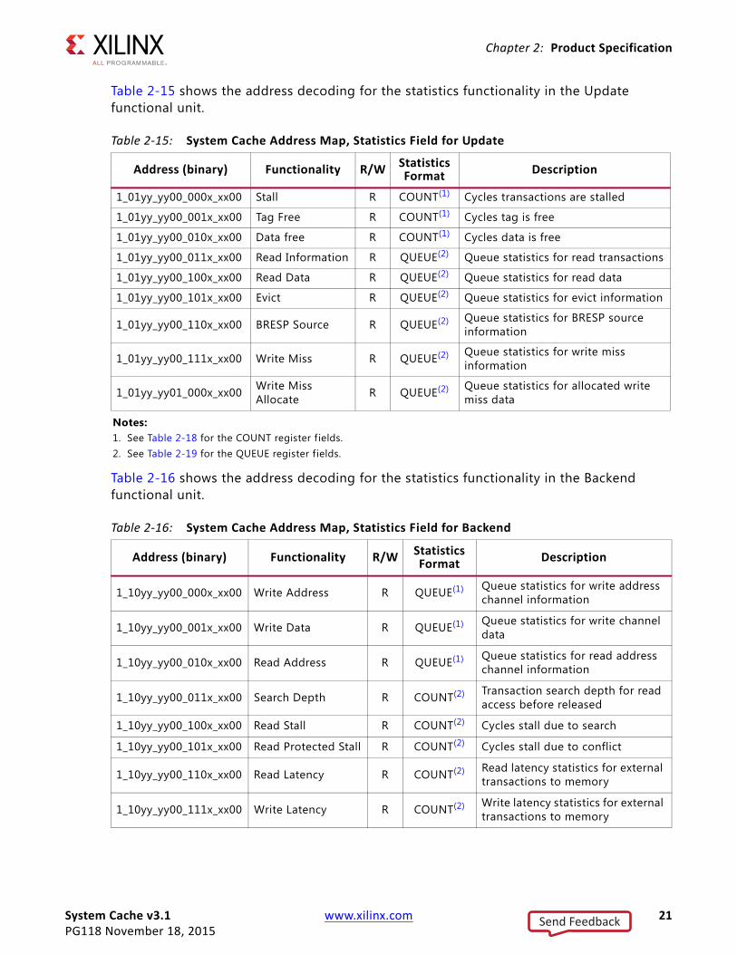
Table 2-15 shows the address decoding for the statistics functionality in the Update functional unit.
Table 2-16 shows the address decoding for the statistics functionality in the Backend functional unit.
Table 2-15: System Cache Address Map, Statistics Field for Update
Address (binary) Functionality R/W Statistics Format Description
1_01yy_yy00_000x_xx00 Stall R COUNT(1) Cycles transactions are stalled
1_01yy_yy00_001x_xx00 Tag Free R COUNT(1) Cycles tag is free
1_01yy_yy00_010x_xx00 Data free R COUNT(1) Cycles data is free
1_01yy_yy00_011x_xx00 Read Information R QUEUE(2) Queue statistics for read transactions
1_01yy_yy00_100x_xx00 Read Data R QUEUE(2) Queue statistics for read data
1_01yy_yy00_101x_xx00 Evict R QUEUE(2) Queue statistics for evict information
1_01yy_yy00_110x_xx00 BRESP Source R QUEUE(2) Queue statistics for BRESP source information
1_01yy_yy00_111x_xx00 Write Miss R QUEUE(2) Queue statistics for write miss information
1_01yy_yy01_000x_xx00 Write Miss Allocate R QUEUE(2) Queue statistics for allocated write
miss data
Notes: 1. See Table 2-18 for the COUNT register f ields.2. See Table 2-19 for the QUEUE register fields.
Table 2-16: System Cache Address Map, Statistics Field for Backend
Address (binary) Functionality R/W StatisticsFormat Description
1_10yy_yy00_000x_xx00 Write Address R QUEUE(1) Queue statistics for write address channel information
1_10yy_yy00_001x_xx00 Write Data R QUEUE(1) Queue statistics for write channel data
1_10yy_yy00_010x_xx00 Read Address R QUEUE(1) Queue statistics for read address channel information
1_10yy_yy00_011x_xx00 Search Depth R COUNT(2) Transaction search depth for read access before released
1_10yy_yy00_100x_xx00 Read Stall R COUNT(2) Cycles stall due to search
1_10yy_yy00_101x_xx00 Read Protected Stall R COUNT(2) Cycles stall due to conflict
1_10yy_yy00_110x_xx00 Read Latency R COUNT(2) Read latency statistics for external transactions to memory
1_10yy_yy00_111x_xx00 Write Latency R COUNT(2) Write latency statistics for external transactions to memory
Send Feedback

System Cache v3.1 www.xilinx.com 22PG118 November 18, 2015
Chapter 2: Product Specification
Table 2-17 shows the address decoding for the statistics functionality in the Control functional unit.
1_10yy_yy01_000x_xx00 Read LatencyConfiguration R/W LONGINT(3)
Configuration for read latency statistics collection. Default value 0. Available modes are defined in Table 2-25
1_10yy_yy01_001x_xx00 Write Latency Configuration R/W LONGINT(3)
Configuration for read latency statistics collection. Default value 4. Available modes are defined in Table 2-26
Notes: 1. See Table 2-19 for the QUEUE register fields.2. See Table 2-18 for the COUNT register f ields.3. See Table 2-20 for the LONGINT register f ields.
Table 2-17: System Cache Address Map, Control
Address (binary) Functionality R/W StatisticsFormat Description
1_11yy_yy00_0000_0x00 Statistics Reset W LONGINT(1) Writing to this register resets all statistic data
1_11yy_yy00_0000_1x00 Statistics Enable R/W LONGINT(1)Configuration for enabling statistics collection. Default value 1. Available modes are defined in Table 2-27
1_11yy_yy00_0001_0x00 Cache Clean W LONGINT(1) Cache line to be cleaned
1_11yy_yy00_0001_1x00 Cache Flush W LONGINT(1) Cache line to be flushed
1_11yy_yy00_0010_0x00 Version Register 0Basic R LONGINT(1)
Basic configuration and version register. Available bit f ields defined in Table 2-28
1_11yy_yy00_0010_1x00 Version Register 1Extended R LONGINT(1)
Extended configuration and version register. Available bit f ields defined in Table 2-30
Notes: 1. See Table 2-20 for the LONGINT register f ields.
Table 2-16: System Cache Address Map, Statistics Field for Backend (Cont’d)
Address (binary) Functionality R/W StatisticsFormat Description
Send Feedback
System Cache v3.1 www.xilinx.com 23PG118 November 18, 2015
Chapter 2: Product Specification
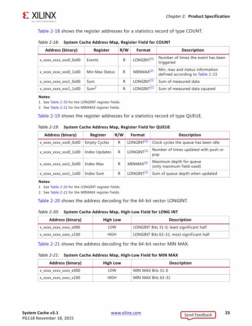
Table 2-18 shows the register addresses for a statistics record of type COUNT.
Table 2-19 shows the register addresses for a statistics record of type QUEUE.
Table 2-20 shows the address decoding for the 64-bit vector LONGINT.
Table 2-21 shows the address decoding for the 64-bit vector MIN MAX.
Table 2-18: System Cache Address Map, Register Field for COUNT
Address (binary) Register R/W Format Description
x_xxxx_xxxx_xxx0_0x00 Events R LONGINT(1) Number of times the event has been triggered
x_xxxx_xxxx_xxx0_1x00 Min Max Status R MINMAX(2) Min, max and status information defined according to Table 2-23
x_xxxx_xxxx_xxx1_0x00 Sum R LONGINT(1) Sum of measured data
x_xxxx_xxxx_xxx1_1x00 Sum2 R LONGINT(1) Sum of measured data squared
Notes: 1. See Table 2-20 for the LONGINT register f ields.2. See Table 2-21 for the MINMAX register f ields.
Table 2-19: System Cache Address Map, Register Field for QUEUE
Address (binary) Register R/W Format Description
x_xxxx_xxxx_xxx0_0x00 Empty Cycles R LONGINT(1) Clock cycles the queue has been idle
x_xxxx_xxxx_xxx0_1x00 Index Updates R LONGINT(1) Number of times updated with push or pop
x_xxxx_xxxx_xxx1_0x00 Index Max R MINMAX(2) Maximum depth for queue(only maximum field used)
x_xxxx_xxxx_xxx1_1x00 Index Sum R LONGINT(1) Sum of queue depth when updated
Notes: 1. See Table 2-20 for the LONGINT register f ields.2. See Table 2-21 for the MINMAX register f ields.
Table 2-20: System Cache Address Map, High-Low Field for LONG INT
Address (binary) High Low Description
x_xxxx_xxxx_xxxx_x000 LOW LONGINT Bits 31-0, least signif icant half
x_xxxx_xxxx_xxxx_x100 HIGH LONGINT Bits 63-32, most signif icant half
Table 2-21: System Cache Address Map, High-Low Field for MIN MAX
Address (binary) High Low Description
x_xxxx_xxxx_xxxx_x000 LOW MIN MAX Bits 31-0
x_xxxx_xxxx_xxxx_x100 HIGH MIN MAX Bits 63-32
Send Feedback

System Cache v3.1 www.xilinx.com 24PG118 November 18, 2015
Chapter 2: Product Specification
Table 2-22 shows the LONG INT register bit f ield definition.
Table 2-23 shows the MIN MAX register bit f ield definition.
Table 2-24 shows the MIN MAX register f ield definitions.
Table 2-25 shows the mode definitions for read latency measurements.
Table 2-26 shows the mode definitions for write latency measurements.
Table 2-22: LONG INT Register Bit Allocation
Long Integer
63 0
Table 2-23: MIN MAX Register Bit Allocation
Min Max Reserved Full Overflow
63 48 47 32 31 2 1 0
Table 2-24: MIN MAX Field Definition
Field Description
Min Minimum unsigned measurement encountered
Max Maximum unsigned measurement encountered, saturates when 0xFFFF is reached
Full Flag if number of concurrent events of the measured type has been reached, indicating that the resulting statistics are inaccurate.
OverflowFlag if measurements have been saturated; this means the statistics results are less accurate. Both average and standard deviation measurements will be lower than the actual values.
Table 2-25: Read Latency Measurement
Value Description0 AR channel valid until f irst data is acknowledged
1 AR channel acknowledged until f irst data is acknowledged
2 AR channel valid until last data is acknowledged
3 AR channel acknowledged until last data is acknowledged
Table 2-26: Write Latency Measurement
Value Description0 AW channel valid until f irst data is written
1 AW channel acknowledged until f irst data is written
2 AW channel valid until last data is written
3 AW channel acknowledged until last data is written
4 AW channel valid until BRESP is acknowledged
5 AW channel acknowledged until BRESP is acknowledged
Send Feedback

System Cache v3.1 www.xilinx.com 25PG118 November 18, 2015
Chapter 2: Product Specification
Table 2-27 shows the mode definitions for statistics enable.
Table 2-28 shows the bit f ield definition of the Version Register 0.
Table 2-29 shows the version register f ield definitions.
Table 2-27: Statistics Enable Configuration
Value Description0 Statistics collection disabled
1 Statistics collection enabled
Table 2-28: Version Register 0 Bit Allocation
Reserved VR Generic Optimized Exclusive Coherent Statistics Version
63 32 31 30 29 25 24 20 19 18 17 16 15 8 7 0
Table 2-29: Version Register 0 Field Definition
Field Description
VR
Version Registers available:0 - Basic register set, only this register1 - Full register set, this and register1, see Table 2-302 and 3 are reserved
Generic
Number of Generic port implemented:0 - All disabled1 to 16- Number of ports implemented17 to 31 are reserved
Optimized
Number of Optimized port implemented:0 - All disabled1 to 16- Number of ports implemented17 to 31 are reserved
Exclusive
Internal Exclusive monitor implementation:0 - Disabled1 - Enabled2 to 3 are reserved
Coherent
Cache coherency implementation:0 - Disabled1 - Enabled2 to 3 are reserved
Send Feedback
System Cache v3.1 www.xilinx.com 26PG118 November 18, 2015
Chapter 2: Product Specification
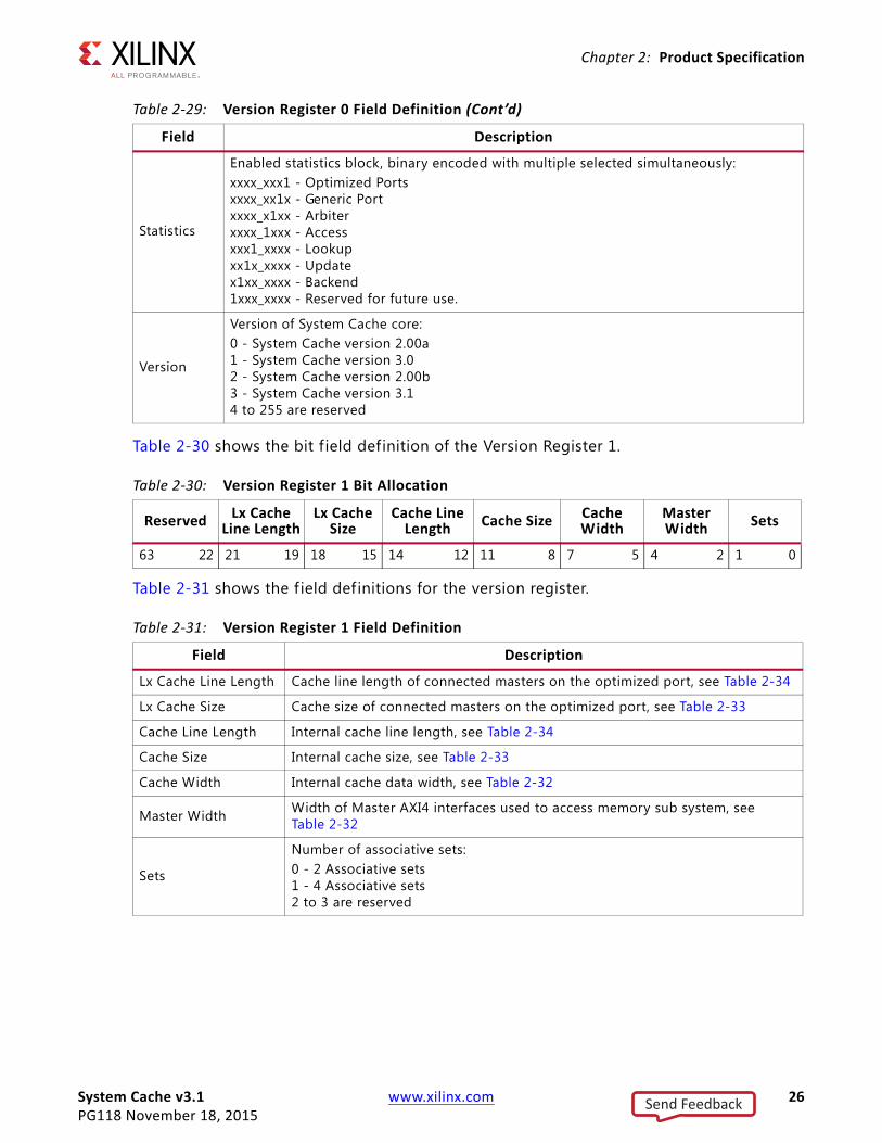
Table 2-30 shows the bit f ield definition of the Version Register 1.
Table 2-31 shows the f ield definitions for the version register.
Statistics
Enabled statistics block, binary encoded with multiple selected simultaneously:xxxx_xxx1 - Optimized Portsxxxx_xx1x - Generic Portxxxx_x1xx - Arbiterxxxx_1xxx - Accessxxx1_xxxx - Lookupxx1x_xxxx - Updatex1xx_xxxx - Backend1xxx_xxxx - Reserved for future use.
Version
Version of System Cache core:0 - System Cache version 2.00a1 - System Cache version 3.02 - System Cache version 2.00b3 - System Cache version 3.14 to 255 are reserved
Table 2-30: Version Register 1 Bit Allocation
Reserved Lx Cache Line Length
Lx Cache Size
Cache Line Length Cache Size Cache
WidthMaster Width Sets
63 22 21 19 18 15 14 12 11 8 7 5 4 2 1 0
Table 2-31: Version Register 1 Field Definition
Field Description
Lx Cache Line Length Cache line length of connected masters on the optimized port, see Table 2-34
Lx Cache Size Cache size of connected masters on the optimized port, see Table 2-33
Cache Line Length Internal cache line length, see Table 2-34
Cache Size Internal cache size, see Table 2-33
Cache Width Internal cache data width, see Table 2-32
Master Width Width of Master AXI4 interfaces used to access memory sub system, see Table 2-32
Sets
Number of associative sets:0 - 2 Associative sets1 - 4 Associative sets2 to 3 are reserved
Table 2-29: Version Register 0 Field Definition (Cont’d)
Field Description
Send Feedback

System Cache v3.1 www.xilinx.com 27PG118 November 18, 2015
Chapter 2: Product Specification
Table 2-32 shows the interface and cache data width definitions.
Table 2-33 shows the cache size definitions.
Table 2-34 shows the cache line length definitions.
Table 2-32: Interface and Cache Data WidthValue Description
0 8-bit data interface and path
1 16-bit data interface and path
2 32-bit data interface and path
3 64-bit data interface and path
4 128-bit data interface and path
5 256-bit data interface and path
6 512-bit data interface and path
7 1024-bit data interface and path
Table 2-33: Cache SizeValue Description
0 64 byte cache size
1 128 byte cache size
2 256 byte cache size
3 512 byte cache size
4 1K byte cache size
5 2K byte cache size
6 4K byte cache size
7 8K byte cache size
8 16K byte cache size
9 32K byte cache size
10 64K byte cache size
11 128K byte cache size
12 256K byte cache size
13 512K byte cache size
14 1M byte cache size
15 2M byte cache size
Table 2-34: Cache Line Length
Value Description0 4 word cache line
1 8 word cache line
2 16 word cache line
3-7 Reserved
Send Feedback

System Cache v3.1 www.xilinx.com 28PG118 November 18, 2015
Chapter 3
Designing with the CoreThis chapter includes guidelines and additional information to facilitate designing with the core. The descriptions herein are MicroBlaze™ centric, but the end result can usually be achieved in a similar way by any master that can behave like an MicroBlaze from a bus transaction point of view.
System Cache DesignThe System Cache core is a write-back cache with configurable size and set associativity. The configuration determines how the address range for the System Cache core is divided and used, see Figure 3-1.
Cache LinesThe cache size is divided into cache lines, the number of cache lines is determined by cache size (C_CACHE_SIZE) divided by line length in bytes (4 * C_CACHE_LINE_LENGTH). In the System Cache core storage, data inside a cache line is accessed by the offset bits of an address.
SetsSeveral cache lines, determined by C_NUM_SETS, are grouped to form a set. Each set is accessed by the index bits part of the address, see Figure 3-1. An address can be mapped to any of the cache lines, also called ways, in a set. The way that is used when allocating a cache line is f irstly any free way in a set, secondly already allocated lines replace by a Least Recently Used (LRU) algorithm.
X-Ref Target - Figure 3-1
Figure 3-1: Address Bit Usage
Offset BitsIndex BitsTag Bits
Full AXI4 Address
Send Feedback

System Cache v3.1 www.xilinx.com 29PG118 November 18, 2015
Chapter 3: Designing with the Core
TagsA cache line tag consists of the tag bits part of the address and flag bits that determine the status of the cache line, for example if it is valid or dirty. See Figure 3-2 for tag contents.
General Design GuidelinesThe are no golden settings to achieve maximum performance for all cases, as performance is application and system dependent. This chapter contains general guidelines that should be considered when configuring the System Cache core and other IP cores to improve performance.
AXI4 Data WidthsAXI4 Data widths should match wherever possible. Matching widths results in minimal area overhead and latency for the AXI4 interconnects.
AXI4 ClockingThe System Cache core is fully synchronous. Using the same clock for all the AXI4 ports removes the need for clock conversion blocks and results in minimal area overhead and latency for the AXI4 interconnects.
Frequency and Hit RateIncreased cache hit rate results in higher performance.
The system cache size should be configured to be larger than the connected L1 caches to achieve any improvements. Increasing the system cache size increases hit rate and has a positive effect on performance. The downside of increasing the system cache size is an increased number of FPGA resources being used. Higher set associativity usually increases the hit rate and the application performance.
The maximum frequency of MicroBlaze is affected by its cache sizes. Smaller MicroBlaze cache sizes usually means that MicroBlaze can meet higher frequency targets. The sweet spot for the frequency versus cache size trade-off when using the System Cache core occurs when configuring MicroBlaze caches to either 256 or 512 bytes, depending on other
X-Ref Target - Figure 3-2
Figure 3-2: Cache Line Tag Contents
Flags Tag Bits
Send Feedback

System Cache v3.1 www.xilinx.com 30PG118 November 18, 2015
Chapter 3: Designing with the Core
MicroBlaze configuration settings. The key to improve frequency is to implement MicroBlaze cache tags with distributed RAM.
Enabling the MicroBlaze Branch Target Cache can improve performance but might reduce the maximum obtainable frequency. Depending on the rest of the MicroBlaze configuration smaller BTC sizes, such as 32 entries (C_BRANCH_TARGET_CACHE_SIZE = 3), should be considered.
MicroBlaze advanced cache features can be used to tweak performance but they are only available in non coherent configurations. Enabling MicroBlaze victim caches increases MicroBlaze cache hit rates, with improved performance as a result. Enabling victim caches can however reduce MicroBlaze maximum frequency in some cases. Instruction stream cache should be disabled, because it usually reduces performance when connected to the System Cache core. MicroBlaze performance is often improved by using 8-word cache lines on the Instruction Cache and Data Cache.
BandwidthUsing wider AXI4 interfaces increases data bandwidth, but also increases FPGA resource usage. Using the widest possible common AXI4 data width between the System Cache AXI4 Master and the external memory gives the highest possible bandwidth. This also applies to the AXI4 connection between MicroBlaze caches and the System Cache core. The widest possible common width gives the highest bandwidth.
ArbitrationThe System Cache core arbitration scheme is round-robin. When the selected port does not have a pending transaction, the f irst port with an available transaction is scheduled, taking the optimized ports in ascending numeric order and then the Generic ports in ascending numeric order.
Address MapThe most common case is when the System Cache core is connected to one memory controller. In this case the System Cache core should have the exact same address range as the memory controller. An example with single memory controller is shown in Figure 3-3.
Send Feedback

System Cache v3.1 www.xilinx.com 31PG118 November 18, 2015
Chapter 3: Designing with the Core
When the System Cache core is connected to multiple slaves it normally has an address range that spans the complete range of all the slaves. Depending on how many slaves there are and their individual address ranges this could leave holes in the address map, which the software designer must be aware of to avoid program issues. An example with a dual memory controller having a hidden address hole is shown in Figure 3-4.
Cache CoherencyEnable cache coherency when a multi processor system is expected to work on the same data, and hardware support for cache coherence is desired for efficiency and safety. This handles all coherency support that is required for Branch Target Cache, MMU as well as Instruction and Data caches. Without the hardware cache coherency support all this has to be handled through software.
Back-door DMAWhen the System Cache core shares the memory controller(s) with at least one other master, a back-door DMA connection is opened up, Figure 3-5 shows a configuration with one additional master. This back-door connection creates issues with data visibility: if an address is allocated in the System Cache core it hides data newly updated by MicroBlaze
X-Ref Target - Figure 3-3
Figure 3-3: Single Memory Controller Configuration
X-Ref Target - Figure 3-4
Figure 3-4: Dual Memory Controller Configuration with Hole
Mem Ctrl
0x8000_00000x807F_FFFF
SystemCache
0x8000_00000x807F_FFFF
AXI4Interconnect
MicroBlaze
M_AXI_DC
M_AXI_IC
Mem Ctrl
0x8000_00000x807F_FFFF
SystemCache
0x8000_00000x81FF_FFFF
AXI4Interconnect
MicroBlaze
M_AXI_DC
M_AXI_IC
Mem Ctrl
0x8100_00000x81FF_FFFF
Send Feedback

System Cache v3.1 www.xilinx.com 32PG118 November 18, 2015
Chapter 3: Designing with the Core
from the other masters that access the memory directly, because the System Cache core uses a write-back storage policy. Similarly, updates from other masters to main memory are hidden from MicroBlaze due to the system cache allocation, which provides the obsolete data that has been previously allocated.
There are multiple solutions to the issues that arise from this system design, depending on the System Cache core configuration. All methods are designed to make sure that an address is not allocated in any of the cache lines in a set.
With Cache CoherencyCache coherency enables communication directly from MicroBlaze to the System Cache core with sideband information. In this case the MicroBlaze code can use the WDC.EXT instructions. There are two types of cache maintenance operations, flush or clear, that can be used depending on how dirty data in the System Cache core for this memory region is handled.
Flush is used when the old data should be retained. This is useful for keeping the old data when the memory region is only partially or sparsely updated from the other master. A flush operation must be used before the other master writes new data or new data might be lost when flushing the system cache. Flush is also used to make sure data written from a MicroBlaze is also visible to the other back-door masters.
Clear should be used when the old data is no longer needed or before the entire memory region is completely updated. Clear operations are typically faster than flush because they do not add transactions on the M_AXI interface of the System Cache core, which have the potential of introducing stall conditions depending on utilization level.
X-Ref Target - Figure 3-5
Figure 3-5: Back-Door DMA Connection with One Additional Master
MemoryController
SystemCache
AXI4Interconnect
MicroBlaze
M_AXI_DC
M_AXI_IC
AXI4 Master
Send Feedback

System Cache v3.1 www.xilinx.com 33PG118 November 18, 2015
Chapter 3: Designing with the Core
With Control InterfaceThe control interface can be used when cache coherency is not implemented or if a master not connected to one of the Optimized ACE ports should handle the cache maintenance. Both Flush and Clear type of operations are available by writing to registers on the control interface. The rules for when Flush or Clear should be used are the same as for the cache coherent case.
The cache maintenance operations from the control port have lower priority than ordinary transactions from the Optimized and Generic ports. Due to this they can be slower than the equivalent cache coherent counterpart if the cache load remains high during cache maintenance.
Without Cache Coherency and Control InterfaceWhen neither cache maintenance, through the Optimized ACE ports, nor Control interface are available, cache lines can still be evicted but with less control and more overhead. This eviction is achieved by reading enough dummy data to ensure that an address is evicted from any of the Cache Lines in a Set that the address can be mapped to. The amount of dummy data that needs to be read equals the set associativity that is implemented.
Preferably the dummy data should be located a multiple of the System Cache core cache size away from the memory region that needs to be cleared. From this point the dummy reads should be performed with a distance of the system cache size (C_CACHE_SIZE) divided by number of sets association (C_NUM_SETS). This has to be repeated for each cache line that is covered by the memory region that should be cleared.
For large memory regions it is probably easiest to read data in a system cache sized memory region with a step size of the system cache line length in bytes (4 * C_CACHE_LINE_LENGTH). As this method is equivalent to a flush cache maintenance operation it has to be performed before another master updates the memory locations in question, otherwise old dirty data could potentially overwrite the new data as cache lines are evicted.
ClockingThe System Cache core is fully synchronous with all interfaces and the internal function clocked by the ACLK input signal. It is advisable to avoid asynchronous clock transitions in the system as they add latency and consumes area resources.
Send Feedback

System Cache v3.1 www.xilinx.com 34PG118 November 18, 2015
Chapter 3: Designing with the Core
ResetsThe System Cache core is reset by the ARESETN input signal. ARESETN is synchronous to ACLK and needs be asserted one ACLK cycle to take affect. The System Cache core is ready for statistic register operation three ACLK cycles after ARESETN is deasserted. Before the System Cache core is available for general data access the entire memory is cleared, that is, all previous content is discarded. The time it takes to clear the cache depends on the configuration; the approximate time is 2*C_CACHE_SIZE/(4*C_CACHE_LINE_LENGTH) clock cycles.
Protocol DescriptionAll interfaces to the System Cache core adhere to the AXI4, AXI4-Lite and ACE protocols with limitations.
MicroBlaze Optimized AXI4 Slave InterfaceThe System Cache core has 16 AXI4 interfaces optimized for accesses performed by the cache interfaces on MicroBlaze. Because MicroBlaze has one AXI4 interface for the instruction cache and one for the data cache, systems with up to eight MicroBlaze processors can be fully connected.
By using a 1:1 AXI4 interconnect to directly connect MicroBlaze and the System Cache core, access latency for MicroBlaze cache misses is reduced, which improves performance. The optimization to only handle the types of AXI4 accesses issued by MicroBlaze simplif ies the implementation, saving area resources as well as improving performance. The data widths of the MicroBlaze optimized interfaces are parameterized to match the data widths of the connected MicroBlaze processors. With wide interfaces the MicroBlaze cache line length normally determines the data width.
The Optimized AXI4 slave interfaces are compliant to a subset of the AXI4 interface specification. The interface includes the subsequent features and exceptions:
• Support for 32-, 128-, 256-, and 512-bit data widths
• Support for some AXI4 burst types and sizes
° No support for FIXED bursts
° WRAP bursts corresponding to the MicroBlaze cache line length, that is, either 4, 8 or 16 beats
° Single beat INCR burst, or either 4, 8 or 16 beats corresponding to the MicroBlaze cache line length
Send Feedback

System Cache v3.1 www.xilinx.com 35PG118 November 18, 2015
Chapter 3: Designing with the Core
° Exclusive accesses are treated as a normal accesses, never returning EXOKAY, unless the internal exclusive monitor is enabled
° Only support for native transaction size, that is, same as data width for the port
• Only support for burst transactions that are contained within a single cache line in the System Cache core
• AXI4 user signals are not supported
• All transactions executed in order regardless of thread ID value. No read reordering or write reordering is implemented.
MicroBlaze Optimized ACE Slave InterfaceThe optimized AXI4 interfaces are replaced by ACE point-to-point connections when cache coherency is enabled. They are optimized for accesses performed by the cache interfaces on MicroBlaze. Eight MicroBlaze processors are supported with coherency enabled.
The Optimized ACE slave interfaces are compliant to a subset of the ACE interface specification. The interface includes the subsequent features and exceptions:
• Support for 32-bit data width
• Support for some ACE burst types and sizes
° No support for FIXED bursts
° Protection bits ignored, that is no expansion of address space due to secure/non-secure handling
° Only sharable transactions are supported
° WRAP bursts corresponding to the MicroBlaze cache line length, that is, either 4, 8 or 16 beats
° Single beat INCR burst, or either 4, 8 or 16 beats corresponding to the MicroBlaze cache line length
° AR channel supports ReadOnce, ReanClean, CleanUnique, CleanInvalid, MakeInvalid and DVM transactions
° Support for propagation of CleanInvalid and MakeInvalid to peer or downstream caches
° AW channel supports WriteUnique only
° Exclusive accesses are only supported for sharable transactions, that is, with ACE transactions exchange
° Only support for native transaction size bursts, that is, same as data width for the port. Single beat support for all sizes
Send Feedback

System Cache v3.1 www.xilinx.com 36PG118 November 18, 2015
Chapter 3: Designing with the Core
• Only support for burst transactions that are contained within a single cache line in the System Cache core
• Only support for Write-Through cache in MicroBlaze
• AXI4 user signals are not supported
• All transactions executed in order regardless of thread ID value. No read reordering or write reordering is implemented.
Generic AXI4 Slave InterfaceTo handle several AXI4 masters in a system two methods are available: either an AXI4 interconnect is used to share the single Generic AXI4 slave interface on the System Cache core or, alternatively, multiple Generic AXI4 interfaces are used (most commonly one per master that needs access). The Generic AXI4 interface has a configurable data width to eff iciently match the connected AXI4 masters. This ensures that both the system area and the AXI4 access latency are reduced.
The Generic AXI4 slave interface is compliant to the full AXI4 interface specif ication. The interface includes the subsequent features and exceptions:
• Support for 32-, 64-, 128-, 256-, and 512-bit data widths
• Support for all AXI4 burst types and sizes
° FIXED bursts are handled as INCR type burst operations (no QUEUE burst capability)
° Up to 16 beats for WRAP bursts
° Up to 16 beats for FIXED bursts (treated as INCR burst type)
° Up to 256 beats for INCR burst
° Exclusive accesses are treated as a normal accesses, never returning EXOKAY, unless the internal exclusive monitor is enabled
• Support for burst sizes that are less than the data width, that is, narrow bursts
• AXI4 user signals are not supported
• All transactions executed in order regardless of thread ID value. No read reordering or write reordering is implemented.
Memory Controller AXI4 Master InterfaceThe AXI4 master interface is used to connect the external memory controller. The data width of the interface can be parameterized to match the data width of the AXI4 slave interface on the memory controller. For best performance and resource usage, the parameters on the interface and the Memory Controller should match.
Send Feedback

System Cache v3.1 www.xilinx.com 37PG118 November 18, 2015
Chapter 3: Designing with the Core
The Memory Controller AXI4 master interface is compliant to the AXI4 interface specification. The interface includes the subsequent features:
• Support for 32-, 64-, 128-, 256-, and 512-bit data widths
• Generates the following AXI4 burst types and sizes
° 2 - 16 beats for WRAP bursts
° 1 - 16 beats for INCR burst
• AXI4 user signals are not provided
• A single thread ID value is generated
Send Feedback

System Cache v3.1 www.xilinx.com 38PG118 November 18, 2015
Chapter 4
Design Flow StepsThis chapter describes customizing and generating the core, constraining the core, and the simulation, synthesis and implementation steps that are specific to this IP core. More detailed information about the standard Vivado® design flows and the IP integrator can be found in the following Vivado Design Suite user guides:
• Vivado Design Suite User Guide: Designing IP Subsystems using IP Integrator (UG994) [Ref 2]
• Vivado Design Suite User Guide: Designing with IP (UG896) [[Ref 3]
• Vivado Design Suite User Guide: Getting Started (UG910) [Ref 4]
• Vivado Design Suite User Guide: Logic Simulation (UG900) [Ref 5]
Customizing and Generating the CoreThis section includes information on using Xilinx tools to customize and generate the core in the Vivado® Design Suite.
If you are customizing and generating the core in the Vivado IP integrator, see the Vivado Design Suite User Guide: Designing IP Subsystems using IP Integrator (UG994) [Ref 2] for detailed information. IP integrator might auto-compute certain configuration values when validating or generating the design. To check whether the values do change, see the description of the parameter in this chapter. To view the parameter value you can run the validate_bd_design command in the Tcl console.
You can customize the IP for use in your design by specifying values for the various parameters associated with the IP core using the following steps:
1. Select the IP from the IP catalog.
2. Double-click the selected IP or select the Customize IP command from the toolbar or right-click menu.
For details, see the Vivado Design Suite User Guide: Designing with IP (UG896) [Ref 3] and the Vivado Design Suite User Guide: Getting Started (UG910) [Ref 4].
Send Feedback

System Cache v3.1 www.xilinx.com 39PG118 November 18, 2015
Chapter 4: Design Flow Steps
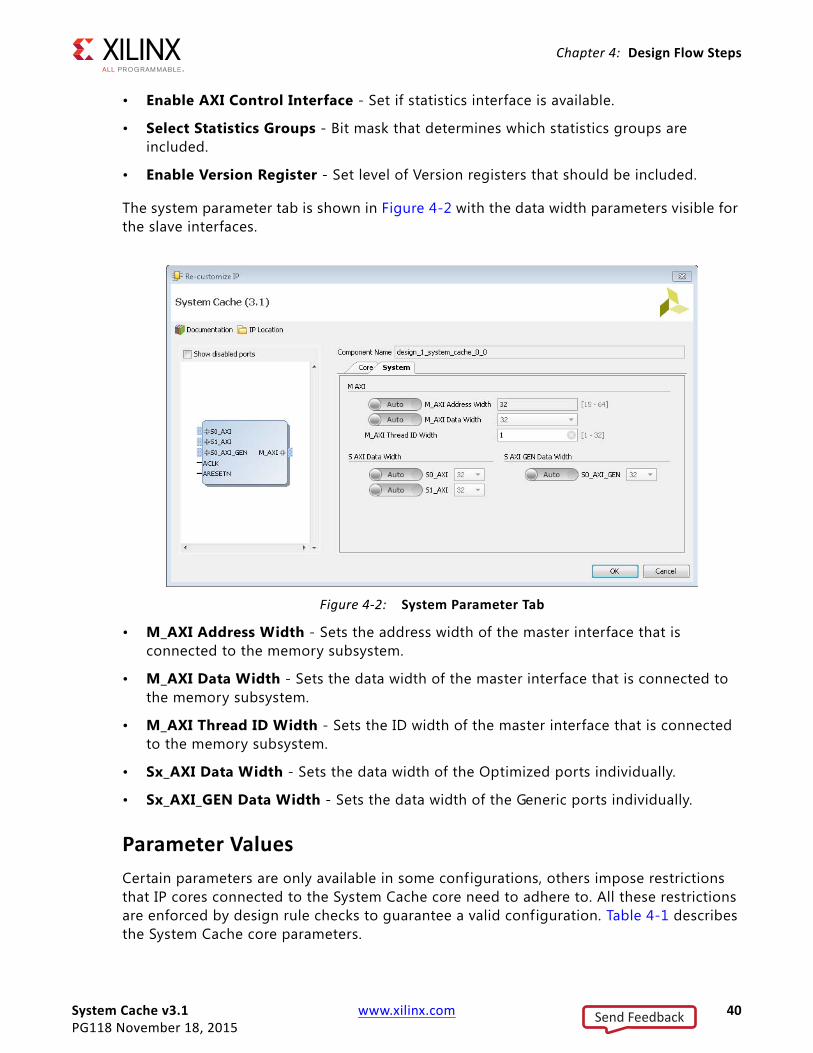
The System Cache core parameters are divided info two categories: core and system. See Table 4-1 for allowed values. The core parameter tab is shown in Figure 4-1.
Note: Figures in this chapter are illustrations of the Vivado IDE. This layout might vary from the current version.
• Number of Optimized AXI4 Ports - Sets the number of optimized ports that are available to connect to a MicroBlaze™ or equivalent IP in terms of AXI4/ACE transaction support.
• Number of Generic AXI4 Ports - Set the number of Generic AXI4 ports that are available for IPs not adhering to the AXI4 subset required for an optimized port, such as DMA.
• Enable Cache Coherency - Enables cache coherency for the optimized ports.
• Enable Exclusive Monitor - Enables Exclusive handling for non-coherent implementation.
• Number of Associative Sets - Specify how many sets the associativity uses.
• Line Length - Cache line length is f ixed to 16.
• Size - Sets the size of the system cache in bytes.
X-Ref Target - Figure 4-1
Figure 4-1: Core Parameter Tab
Send Feedback
System Cache v3.1 www.xilinx.com 40PG118 November 18, 2015
Chapter 4: Design Flow Steps
• Enable AXI Control Interface - Set if statistics interface is available.
• Select Statistics Groups - Bit mask that determines which statistics groups are included.
• Enable Version Register - Set level of Version registers that should be included.
The system parameter tab is shown in Figure 4-2 with the data width parameters visible for the slave interfaces.
• M_AXI Address Width - Sets the address width of the master interface that is connected to the memory subsystem.
• M_AXI Data Width - Sets the data width of the master interface that is connected to the memory subsystem.
• M_AXI Thread ID Width - Sets the ID width of the master interface that is connected to the memory subsystem.
• Sx_AXI Data Width - Sets the data width of the Optimized ports individually.
• Sx_AXI_GEN Data Width - Sets the data width of the Generic ports individually.
Parameter ValuesCertain parameters are only available in some configurations, others impose restrictions that IP cores connected to the System Cache core need to adhere to. All these restrictions are enforced by design rule checks to guarantee a valid configuration. Table 4-1 describes the System Cache core parameters.
X-Ref Target - Figure 4-2
Figure 4-2: System Parameter Tab
Send Feedback

System Cache v3.1 www.xilinx.com 41PG118 November 18, 2015
Chapter 4: Design Flow Steps
The parameter restrictions are:
• Internal cache data width must either be 32 or a multiple of the cache line length of masters connected to the optimized ports (C_CACHE_DATA_WIDTH = 32 or C_CACHE_DATA_WIDTH = n * 32 * C_Lx_CACHE_LINE_LENGTH).
• All optimized slave port data widths must be less than or equal to the internal cache data width (C_Sx_AXI_DATA_WIDTH ≤ C_CACHE_DATA_WIDTH).
• All Generic slave port data widths must be less than or equal to the internal cache data width (C_Sx_AXI_GEN_DATA_WIDTH ≤ C_CACHE_DATA_WIDTH).
• The master port data width must be greater then or equal to the internal cache data width (C_CACHE_DATA_WIDTH ≤ C_M_AXI_DATA_WIDTH).
• The internal cache line length must be greater than or equal to the corresponding cache line length of the AXI4 masters connected to the optimized port (C_CACHE_LINE_LENGTH ≥ C_Lx_CACHE_LINE_LENGTH).
• With cache coherency enabled = only 32-bit data is supported for all parts of the datapath(C_Sx_AXI_DATA_WIDTH = C_CACHE_DATA_WIDTH = C_M_AXI_DATA_WIDTH = 32).
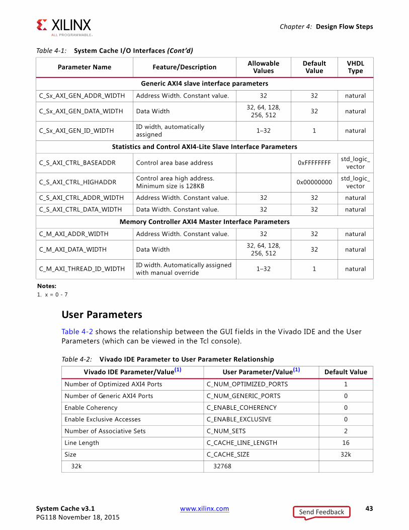
Table 4-1: System Cache I/O Interfaces
Parameter Name Feature/Description AllowableValues
DefaultValue
VHDLType
C_FAMILY FPGA Architecture Supportedarchitectures virtex7 string
C_INSTANCE Instance Name Any instancename system_cache string
C_FREQ System Cache clock frequencyAny valid
frequency forthe device
0 natural
C_BASEADDR Cacheable area base address 0xFFFFFFFF std_logic_vector
C_HIGHADDR Cacheable area high address. Minimum size is 32KB 0x00000000 std_logic_
vector
C_ENABLE_COHERENCY Enable implementation of cache coherent optimized ports 0, 1 0 natural
C_ENABLE_EXCLUSIVEEnable implementation of exclusive monitor for non-coherent implementation
0, 1 0 natural
C_ENABLE_CTRL Enable implementation ofStatistics and Control function 0, 1 0 natural
Send Feedback

System Cache v3.1 www.xilinx.com 42PG118 November 18, 2015
Chapter 4: Design Flow Steps
C_ENABLE_STATISTICS
Bit mask for which statistics groups implemented when Control Interface is enabled:xxxx_xxx1 - Optimized Portsxxxx_xx1x - Generic Portxxxx_x1xx - Arbiterxxxx_1xxx - Accessxxx1_xxxx - Lookupxx1x_xxxx - Updatex1xx_xxxx - Backend1xxx_xxxx - Reserved for future use
0–255 255 natural
C_ENABLE_VERSION_REGISTER
Level of Version Register to include:0 - None1 - Basic2 - Full
0, 1, 2 0 natural
C_NUM_OPTIMIZED_PORTS Number of ports optimized for MicroBlaze cache connection 0–16 1 natural
C_NUM_GENERIC_PORTS Number of ports supporting AXI4 0–16 0 natural
C_NUM_SETS Cache associativity 2, 4 2 natural
C_CACHE_DATA_WIDTHCache data width used internally. Automatically calculated to match AXI4 master interface
32, 64, 128,256, 512 32 natural
C_CACHE_LINE_LENGTH Cache line length. Constant value. 16 16 natural
C_CACHE_SIZE Cache size in bytes32768, 65536,
131072, 262144,524288
32768 natural
C_Lx_CACHE_LINE_LENGTH
Cache line length on masters connected to optimized ports. Automatically assigned with manual override
4, 8, 16 4 natural
C_Lx_CACHE_SIZE
Cache size on masters connected to optimized ports. Automatically assigned with manual override
64, 128, 256,512, 1024,
2048, 4096,8192, 16384,32768, 65536
1024 natural
MicroBlaze cache optimized AXI4 Slave Interface Parameters
C_Sx_AXI_ADDR_WIDTH(1) Address width. Constant value. 32 32 natural
C_Sx_AXI_DATA_WIDTH(1) Data width 32, 128,256, 512 32 natural
C_Sx_AXI_ID_WIDTH(1) ID width, automatically assigned 1–32 1 natural
Table 4-1: System Cache I/O Interfaces (Cont’d)
Parameter Name Feature/Description AllowableValues
DefaultValue
VHDLType
Send Feedback
System Cache v3.1 www.xilinx.com 43PG118 November 18, 2015
Chapter 4: Design Flow Steps
User ParametersTable 4-2 shows the relationship between the GUI f ields in the Vivado IDE and the User Parameters (which can be viewed in the Tcl console).
Generic AXI4 slave interface parameters
C_Sx_AXI_GEN_ADDR_WIDTH Address Width. Constant value. 32 32 natural
C_Sx_AXI_GEN_DATA_WIDTH Data Width 32, 64, 128,256, 512 32 natural
C_Sx_AXI_GEN_ID_WIDTH ID width, automaticallyassigned 1–32 1 natural
Statistics and Control AXI4-Lite Slave Interface Parameters
C_S_AXI_CTRL_BASEADDR Control area base address 0xFFFFFFFF std_logic_vector
C_S_AXI_CTRL_HIGHADDR Control area high address. Minimum size is 128KB 0x00000000 std_logic_
vector
C_S_AXI_CTRL_ADDR_WIDTH Address Width. Constant value. 32 32 natural
C_S_AXI_CTRL_DATA_WIDTH Data Width. Constant value. 32 32 natural
Memory Controller AXI4 Master Interface Parameters
C_M_AXI_ADDR_WIDTH Address Width. Constant value. 32 32 natural
C_M_AXI_DATA_WIDTH Data Width 32, 64, 128,256, 512 32 natural
C_M_AXI_THREAD_ID_WIDTH ID width. Automatically assigned with manual override 1–32 1 natural
Notes: 1. x = 0 - 7
Table 4-1: System Cache I/O Interfaces (Cont’d)
Parameter Name Feature/Description AllowableValues
DefaultValue
VHDLType
Table 4-2: Vivado IDE Parameter to User Parameter Relationship
Vivado IDE Parameter/Value(1) User Parameter/Value(1) Default Value
Number of Optimized AXI4 Ports C_NUM_OPTIMIZED_PORTS 1
Number of Generic AXI4 Ports C_NUM_GENERIC_PORTS 0
Enable Coherency C_ENABLE_COHERENCY 0
Enable Exclusive Accesses C_ENABLE_EXCLUSIVE 0
Number of Associative Sets C_NUM_SETS 2
Line Length C_CACHE_LINE_LENGTH 16
Size C_CACHE_SIZE 32k
32k 32768
Send Feedback

System Cache v3.1 www.xilinx.com 44PG118 November 18, 2015
Chapter 4: Design Flow Steps
Output GenerationFor details, see the Vivado Design Suite User Guide: Designing with IP (UG896) [Ref 3].
Constraining the CoreThis section contains information about constraining the core in the Vivado Design Suite.
Required ConstraintsThis section is not applicable for this IP core.
Device, Package, and Speed Grade SelectionsThis section is not applicable for this IP core.
64k 65536
128k 131072
256k 262144
512k 524288
Enable AXI Control Interface C_ENABLE_CTRL 0
Select Statistics Groups C_ENABLE_STATISTICS 0
Enable Version Registers C_ENABLE_VERSION_REGISTER None
None 0
Basic 1
Full 2
M_AXI Address Width C_M_AXI_ADDR_WIDTH 32
M_AXI Data Width C_M_AXI_DATA_WIDTH 32
M_AXI Thread ID Width C_M_AXI_THREAD_ID_WIDTH 1
Sx_AXI C_Sx_AXI_DATA_WIDTH 32
Sx_AXI_GEN C_Sx_AXI_GEN_DATA_WIDTH 32
Notes: 1. Parameter values are listed in the table where the GUI parameter value differs from the user parameter value. Such
values are shown in this table as indented below the associated parameter.
Table 4-2: Vivado IDE Parameter to User Parameter Relationship (Cont’d)
Vivado IDE Parameter/Value(1) User Parameter/Value(1) Default Value
Send Feedback

System Cache v3.1 www.xilinx.com 45PG118 November 18, 2015
Chapter 4: Design Flow Steps
Clock FrequenciesThis section is not applicable for this IP core.
Clock ManagementThis section is not applicable for this IP core.
Clock PlacementThis section is not applicable for this IP core.
BankingThis section is not applicable for this IP core.
Transceiver PlacementThis section is not applicable for this IP core.
I/O Standard and PlacementThis section is not applicable for this IP core.
SimulationFor comprehensive information about Vivado simulation components, as well as information about using supported third party tools, see the Vivado Design Suite User Guide: Logic Simulation (UG900) [Ref 5].
IMPORTANT: For cores targeting 7 series or Zynq-7000 devices, UNIFAST libraries are not supported. Xilinx IP is tested and qualified with UNISIM libraries only.
Synthesis and ImplementationFor details about synthesis and implementation, see the Vivado Design Suite User Guide: Designing with IP (UG896) [Ref 3].
Send Feedback

System Cache v3.1 www.xilinx.com 46PG118 November 18, 2015
Appendix A
Migrating and UpgradingThis appendix contains information about migrating a design from ISE® to the Vivado® Design Suite, and for upgrading to a more recent version of the IP core. For customers upgrading in the Vivado Design Suite, important details (where applicable) about any port changes and other impact to user logic are included.
Migrating to the Vivado Design SuiteFor information on migrating to the Vivado® Design Suite, see the ISE to Vivado Design Suite Migration Guide (UG911) [Ref 6].
Upgrading in the Vivado Design SuiteThis section provides information about any changes to the user logic or port designations that take place when you upgrade to a more current version of this IP core in the Vivado Design Suite.
Functionality Changes
Version 1.01a, 1.01b and 1.01c
The following describe changes between the ISE version of the core and the current version.
The supported cache sizes has been increased to support 256KB and 512KB.
Hit and miss statistics are changed to be on a per port basis instead of total.
Added support for simultaneously ongoing read for each channel.
Version 2.00a and 3.0
Added cache coherency support on optimized ports.
Added statistics related to cache coherency.
Send Feedback
System Cache v3.1 www.xilinx.com 47PG118 November 18, 2015
Appendix A: Migrating and Upgrading
Added optional exclusive monitor for non-coherent cache implementation.
Added version and cache maintenance registers.
Version 3.1
Increased number of Optimized ports from 8 to 16.
Increased number of Generic ports from 1 to 16.
Added support for 16 word cacheline when coherency is enabled.
Added support for up to 64-bit wide addresses.
Port and Parameter Changes
Version 3.1
Increased number of Optimized ports from 8 to 16.
Increased number of Generic ports from 1 to 16.
Send Feedback

System Cache v3.1 www.xilinx.com 48PG118 November 18, 2015
Appendix B
DebuggingThis appendix includes details about resources available on the Xilinx Support website and debugging tools.
Finding Help on Xilinx.comTo help in the design and debug process when using the System Cache core, the Xilinx Support web page contains key resources such as product documentation, release notes, answer records, information about known issues, and links for obtaining further product support.
DocumentationThis product guide is the main document associated with the System Cachecore. This guide, along with documentation related to all products that aid in the design process, can be found on the Xilinx Support web page or by using the Xilinx Documentation Navigator.
Download the Xilinx Documentation Navigator from the Downloads page. For more information about this tool and the features available, open the online help after installation.
Answer RecordsAnswer Records include information about commonly encountered problems, helpful information on how to resolve these problems, and any known issues with a Xilinx product. Answer Records are created and maintained daily ensuring that users have access to the most accurate information available.
Answer Records for this core can be located by using the Search Support box on the main Xilinx support web page. To maximize your search results, use proper keywords such as
• Product name
• Tool message(s)
• Summary of the issue encountered
A filter search is available after results are returned to further target the results.
Send Feedback

System Cache v3.1 www.xilinx.com 49PG118 November 18, 2015
Appendix B: Debugging
Master Answer Record for the System Cache
AR: 54452
Technical SupportXilinx provides technical support at the Xilinx Support web page for this LogiCORE™ IP product when used as described in the product documentation. Xilinx cannot guarantee timing, functionality, or support if you do any of the following:
• Implement the solution in devices that are not defined in the documentation.
• Customize the solution beyond that allowed in the product documentation.
• Change any section of the design labeled DO NOT MODIFY.
To contact Xilinx Technical Support, navigate to the Xilinx Support web page.
Debug ToolsThere are many tools available to address System Cache design issues. It is important to know which tools are useful for debugging various situations.
Vivado Design Suite Debug FeatureThe Vivado® Design Suite debug feature inserts logic analyzer and virtual I/O cores directly into your design. The debug feature also allows you to set trigger conditions to capture application and integrated block port signals in hardware. Captured signals can then be analyzed. This feature in the Vivado IDE is used for logic debugging and validation of a design running in Xilinx devices.
The Vivado logic analyzer is used to interact with the logic debug IP cores, including:
• ILA 2.0 (and later versions)
• VIO 2.0 (and later versions)
See the Vivado Design Suite User Guide: Programming and Debugging (UG908) [Ref 7].
Reference BoardsAll Xilinx development boards for 7 series FPGAs support System Cache. These boards can be used to prototype designs and establish that the core can communicate with the system.
Send Feedback

System Cache v3.1 www.xilinx.com 50PG118 November 18, 2015
Appendix B: Debugging
Simulation DebugThe simulation debug flow for QuestaSim is described below. A similar approach can be used with other simulators.
• Check for the latest supported versions of QuestaSim in the Xilinx Design Tools: Release Notes Guide. Is this version being used? If not, update to this version.
• If using Verilog, do you have a mixed mode simulation license? If not, obtain a mixed-mode license.
• Ensure that the proper libraries are compiled and mapped. In Xilinx Platform Studio this is done within the tool using Edit > Preferences > Simulation, and in the Vivado Design Suite using Flow > Simulation Settings.
• Have you associated the intended software program for all connected MicroBlaze™ processor with the simulation? Use Project > Select Elf File in Xilinx Platform Studio to do this. Make sure to regenerate the simulation files with Simulation > Generate Simulation HDL Files afterwards. The equivalent command in the Vivado Design Suite is Tools > Associate ELF Files.
• When observing the traff ic on any of the AXI4 interfaces connected to the System Cache core, see the AMBA® AXI and ACE Protocol Specification [Ref 1] for the AXI4 timing.
Hardware DebugHardware issues can range from link bring-up to problems seen after hours of testing. This section provides debug steps for common issues. The Vivado debug feature is a valuable resource to use in hardware debug. The signal names mentioned in the following individual sections can be probed using the debug feature for debugging the specif ic problems.
General ChecksEnsure that all the timing constraints for the core were properly incorporated from the example design and that all constraints were met during implementation.
• Does it work in post-place and route timing simulation? If problems are seen in hardware but not in timing simulation, this could indicate a PCB issue. Ensure that all clock sources are active and clean.
• If using MMCMs in the design, ensure that all MMCMs have obtained lock by monitoring the locked port.
Send Feedback
System Cache v3.1 www.xilinx.com 51PG118 November 18, 2015
Appendix B: Debugging
AXI4 ChecksEither use bus analyzer or connect the relevant AXI4 signals to a logic analyzer in the Vivado debug feature. Make sure the data is captured with ACLK.
Interface Debug
Optimized AXI4 InterfacesOnly the number of ports specif ied by C_NUM_OPTIMIZED_PORTS are available. There are no registers to read, but basic functionality is tested by writing data and then reading it back. Output S<x>_AXI_AWREADY asserts when the write address is used, S<x>_AXI_WREADY asserts when the write data is used, and output S<x>_AXI_BVALID asserts when the write response is valid. Output S<x>_AXI_ARREADY asserts when the read address is used, and output S<x>_AXI_RVALID asserts when the read data/response is valid. If the interface is unresponsive, ensure that the following conditions are met:
• The ACLK input is connected and toggling.
• The interface is not being held in reset, and ARESETN is an active-Low reset.
• Make sure the accessed Optimized port is activated.
• If the simulation has been run, verify in simulation and/or a Vivado debugging tool capture that the waveform is correct for accessing the AXI4 interface.
Generic AXI4 InterfacesOnly the number of ports specif ied by C_NUM_GENERIC_PORTS are available. There are no registers to read, but basic functionality is tested by writing data and then reading it back. Output S<x>_AXI_GEN_AWREADY asserts when the write address is used, S<x>_AXI_GEN_WREADY asserts when the write data is used, and output S<x>_AXI_GEN_BVALID asserts when the write response is valid. Output S<x>_AXI_GEN_ARREADY asserts when the read address is used, and output S<x>_AXI_GEN_RVALID asserts when the read data/response is valid. If the interface is unresponsive, ensure that the following conditions are met:
• The ACLK input is connected and toggling.
• The interface is not being held in reset, and ARESETN is an active-Low reset.
• Make sure the accessed Generic port is activated.
• If the simulation has been run, verify in simulation and/or a Vivado debugging tool capture that the waveform is correct for accessing the AXI4 interface.
Send Feedback
System Cache v3.1 www.xilinx.com 52PG118 November 18, 2015
Appendix B: Debugging
AXI4-Lite InterfacesThe AXI4-Lite interface is only available when the Control interface is enabled with C_ENABLE_CTRL. Read from a register that does not have all 0s as a default to verify that the interface is functional. Output S_AXI_CTRL_ARREADY asserts when the read address is used, and output S_AXI_CTRL_RVALID asserts when the read data/response is valid. If the interface is unresponsive, ensure that the following conditions are met:
• The ACLK input is connected and toggling.
• The interface is not being held in reset, and ARESETN is an active-Low reset.
• If the simulation has been run, verify in simulation and/or a Vivado debugging tool capture that the waveform is correct for accessing the AXI4-Lite interface.
Send Feedback

System Cache v3.1 www.xilinx.com 53PG118 November 18, 2015
Appendix C
Additional Resources and Legal Notices
Xilinx ResourcesFor support resources such as Answers, Documentation, Downloads, and Forums, see Xilinx Support.
ReferencesThese documents provide supplemental material useful with this product guide:
1. AMBA® AXI and ACE Protocol Specification (ARM IHI 0022E)
2. Vivado Design Suite User Guide: Designing IP Subsystems using IP Integrator (UG994)
3. Vivado Design Suite User Guide: Designing with IP (UG896)
4. Vivado Design Suite User Guide: Getting Started (UG910)
5. Vivado Design Suite User Guide - Logic Simulation (UG900)
6. ISE to Vivado Design Suite Migration Guide (UG911)
7. Vivado Design Suite User Guide: Programming and Debugging (UG908)
Send Feedback

System Cache v3.1 www.xilinx.com 54PG118 November 18, 2015
Appendix C: Additional Resources and Legal Notices
Revision HistoryThe following table shows the revision history for this document.
Please Read: Important Legal NoticesThe information disclosed to you hereunder (the "Materials") is provided solely for the selection and use of Xilinx products. To the maximum extent permitted by applicable law: (1) Materials are made available "AS IS" and with all faults, Xilinx hereby DISCLAIMS ALL WARRANTIES AND CONDITIONS, EXPRESS, IMPLIED, OR STATUTORY, INCLUDING BUT NOT LIMITED TO WARRANTIES OF MERCHANTABILITY, NON-INFRINGEMENT, OR FITNESS FOR ANY PARTICULAR PURPOSE; and (2) Xilinx shall not be liable (whether in contract or tort, including negligence, or under any other theory of liability) for any loss or damage of any kind or nature related to, arising under, or in connection with, the Materials (including your use of the Materials), including for any direct, indirect, special, incidental, or consequential loss or damage (including loss of data, profits, goodwill, or any type of loss or damage suffered as a result of any action brought by a third party) even if such damage or loss was reasonably foreseeable or Xilinx had been advised of the possibility of the same. Xilinx assumes no obligation to correct any errors contained in the Materials or to notify you of updates to the Materials or to product specifications. You may not reproduce, modify, distribute, or publicly display the Materials without prior written consent. Certain products are subject to the terms and conditions of Xilinx's limited warranty, please refer to Xilinx's Terms of Sale which can be viewed at http://www.xilinx.com/legal.htm#tos; IP cores may be subject to warranty and support terms contained in a license issued to you by Xilinx. Xilinx products are not designed or intended to be fail-safe or for use in any application requiring fail-safe performance; you assume sole risk and liability for use of Xilinx products in such critical applications, please refer to Xilinx's Terms of Sale which can be viewed at http://www.xilinx.com/legal.htm#tos.Automotive Applications DisclaimerXILINX PRODUCTS ARE NOT DESIGNED OR INTENDED TO BE FAIL-SAFE, OR FOR USE IN ANY APPLICATION REQUIRING FAIL-SAFE PERFORMANCE, SUCH AS APPLICATIONS RELATED TO: (I) THE DEPLOYMENT OF AIRBAGS, (II) CONTROL OF A VEHICLE, UNLESS THERE IS A FAIL-SAFE OR REDUNDANCY FEATURE (WHICH DOES NOT INCLUDE USE OF SOFTWARE IN THE XILINX DEVICE TO IMPLEMENT THE REDUNDANCY) AND A WARNING SIGNAL UPON FAILURE TO THE OPERATOR, OR (III) USES THAT COULD LEAD TO DEATH OR PERSONAL INJURY. CUSTOMER ASSUMES THE SOLE RISK AND LIABILITY OF ANY USE OF XILINX PRODUCTS IN SUCH APPLICATIONS.© Copyright 2013–2015 Xilinx, Inc. Xilinx, the Xilinx logo, Artix, ISE, Kintex, Spartan, Virtex, Vivado, Zynq, and other designated brands included herein are trademarks of Xilinx in the United States and other countries. AMBA, AMBA Designer, ARM, ARM1176JZ-S, CoreSight, Cortex, and PrimeCell are trademarks of ARM in the EU and other countries. All other trademarks are the property of their respective owners.
Date Version Revision
11/18/2015 3.1 • Added support for UltraScale+ families.
06/24/2015 3.1 • Moved performance and resource utilization data to the web
04/01/2015 3.1 • Increased Optimized ports to 16• Increased Generic ports to 16• Added support for 16 word cache line when coherent• Resource tables updated• Support of up to 64-bit address width
10/02/2013 3.0 • Revision number advanced to 3.0 to align with core version number.• Description of new reset behavior • Resource tables updated• Updated latency number for write transactions
03/20/2013 1.0 Initial release as a Product Guide; replaces PG031. No documentation changes for this release.
Send Feedback