Embed Size (px)
Citation preview

POLITECNICO DI MILANO
Facolta di Ingegneria dei Sistemi
Dipartimento di Fisica
Tesi di Laurea in
Ingegneria Fisica
Systematic investigation into the influence
of growth conditions on InAs/GaAs
quantum dot densities and sizes for
intermediate band solar cell application
Relatore Candidato
Prof. Giovanni Isella Stefano Vitelli
Matricola: 719607
Anno Accademico 2009/2010


To my lovely familyVirgilio, Graziella and Luca
to my friend Filippo P.and to my darling Valeria


Abstract
The influence of the conditions during growth of InAs/GaAs quantum-dot structures onGaAs(001) by molecular-beam epitaxy was investigated systematically with respect toachieving high quantum dot densities, homogeneity and narrow sizes distribution. Theseare requirements for obtaining the necessary intermediate band in intermediate band solarcells. The growth temperature, InAs deposit, As flux, growth rate and III/V flux ratiowere varied. Atomic force microscopy and a modular program for SPM data analysis wereused to study the morphological properties of the QDs. The effect of several operationsduring image processing was analysed and a suitable routine was defined. The optimaltemperature for the growth was found to be 480◦C although 420◦C was sufficient to induce2D-3D transition. Varying the InAs thickness, a self-limiting size effect was detected at2.2 ML, while increasing As-flux to 6x10⁻⁶ Torr led to big clasters formation. Finally,low growth rate (0.1-0.5 ML/s) was necessary to keep good homogeneity and the optimalIII/V flux ratio was found to be in the range 1/10 - 1/5.
Sommario
La presente tesi si focalizza sullo studio di punti quantisti InAs/GaAs su substratoGaAs(001) per applicazioni su celle solari a banda intermedia. Un’alta densita di pun-ti quantistici, una buona omogeneita e una distribuzione stretta di dimensioni laterali ealtezze sono requisiti necessari per ottenere la banda intermedia in questa specifica ap-plicazione. I campioni sono cresciuti per mezzo di epitassia da fasci molecolari, variandosistematicamente i parametri di crescita quali temperatura, quantita di InAs depositato,flusso di As, velocita di crescita e rapporto III/V di flussi. Lo scopo di questo studio eanalizzare l’influenza di questi parametri su densita, distribuzioni di dimensioni e omo-geneita dei punti quantistici.I profili 3D della superficie dei campioni sono estratti tramite microscopia a forza atom-ica; successivamente le informazioni sono estrapolate dalle immagini per mezzo di unospecifico programma di analisi dopo aver valutato l’effetto di diverse correzioni durantel’image processing e dopo aver definito un’opportuna routine.E stato dimostrato che la temperatura ottimale di crescita e 480◦C, sebbene 420◦C sianosufficienti per indurre la transizione 2D-3D. Variando lo spessore di InAs, a 2.2 ML e statonotato un effetto auto-limitante per quanto riguarda le dimensioni, mentre aumentandoil flusso di As fino a 6x10⁻⁶ Torr si induce la coalescenza di piu punti quantistici. In-fine, basse velocita di crescita (0.1-0.5 ML/s) sono necessarie per mantenere una buonaomogeneita e il rapporto ottimale III/V e nell’intervallo 1/10-1/5.


Estratto in italiano
In questo studio viene analizzata l’influenza dei parametri di crescita epitassiale sulle pro-prieta morfologiche di punti quantistici InAs/GaAs cresciuti su substrato GaAs(001), perapplicazioni su celle solari a banda intermedia (IBSC).
Nel capitolo 1, sono presentate le tre generazioni fotovoltaiche.Alla prima generazione appartengono tutte le celle solari a singola giunzione basate sulsilicio, sviluppate sulla base di strutture e processi relativamente semplici. Quando questatecnologia e maturata, i costi del prodotto finito sono stati dominati dai costi delle ma-terie prime (wafer di silicio e incapsulanti). Durante gli scorsi 20 anni si e assistito ad uncambiamento verso la seconda generazione o tecnologia dei film sottili. Questa tecnologiaoffre la possibilita di ridurre i costi dei materiali eliminando il wafer di silicio, rendendopraticamente ogni semiconduttore sufficientemente economico. Inoltre, un altro vantag-gio riguarda il fatto di poter aumentare l’unita produttiva di 100 volte. Al momento 5differenti tecnologie sono giunte allo stadio di sviluppo commerciale:
• Lega idrogenata di silicio amorfo
• Silicio policristallino
• Composti policristallini: calcopirati
• Diossido di titanio nanocristallino
• Tellurio di cadmio
Col passare del tempo, pero, i costi saranno progressivamente dominati da quelli dei mate-riali costituenti. Per poter progredire ulteriormente, l’efficienza di conversione dovra essereaumentata sostanzialmente. Le performance delle celle solari potrebbero essere accresciutedi 2-3 volte se fossero utilizzati differenti concetti per produrre la terza generazione. Perora, quelli studiati sono:
• Celle tandem
• Generazione multipla di coppie e-h per fotone
• Celle hot carriers
• Celle con multibanda e impurita
• Celle termofotovoltaiche e termofotoniche
vii

Nel capitolo 2, viene presentata la fisica delle celle solari a banda intermedia (IBSC).Una IBSC e un’apparecchiatura fotovoltaica capace di superare l’efficienza limite di unacella solare a gap singola, sfruttando le proprieta elettriche e ottiche di un materiale abanda intermedia (IB). Questo tipo di materiale prende il nome dall’esistenza di unabanda elettronica extra situata nel mezzo del bandgap. L’IB divide il bandgap in dueintervalli di energia proibiti. Quando viene assorbita la luce in questa IB , oltra allaconvenzionale transizione elettronica dalla banda di valenza (VB) alla banda di conduzione(CB), vi sono altre due transizioni possibili: dalla VB alla IB e dalla IB alla CB. Questoprincipio quindi, permette di utilizzare un maggiore spettro della radiazione solare perla conversione, assorbendo fotoni a frequenze che sarebbero perdute in una cella solareconvenzionale.Al momento ci sono tre differenti approcci per produrre una IBSC:
• Sintesi diretta di un materiale con IB
• L’approccio nanoporoso
• Implementazione per mezzo di punti quantistici (QD-IBSC)
Quest’ultima tecnica e stata utilizzata nel nostro studio.Per poter capire come e possibile ottenere una IB, basti pensare alle proprieta quantistichedi questa nanostruttura. Essa presenta livelli energetici discreti simili a quelli di un atomo.Per questo motivo i punti quantistici sono anche chiamati atomi artificiali. Posizionandole nanostrutture in array 3D ordinati, le funzioni d’onda possono sovrapporsi e dare luogoad uno splitting simile a quello che si ha nei cristalli costituiti da atomi convenzionali.Cosı facendo e possibile generare la banda intermedia richiesta per mezzo di questi super-reticoli.Esistono alcune considerazioni pratiche riguardo l’implementazione delle QD-IBSC:
• Il raggio delle nanostrutture dovrebbe essere dell’ordine dei 3.9 nm. In linea di prin-cipio tale dimensione potrebbe essere raggiungibile utilizzando il metodo di crescitaStranki-Krastanov per mezzo dell’ MBE
• La densita dei punti quantistici dovrebbe essere la piu elevata possibile
• Le nanostrutture dovrebbero essere le piu identiche possibili
E quindi importante riuscire a controllare queste caratteristiche delle nanostrutture.
Nel capitolo 3 si e provveduto a descrivere i principali processi fisici coinvolti durantela crescita di punti quantistici InAs/GaAs per mezzo di MBE secondo la tecnica Stanski-Krastanov (S-K). La descrizione segue le varie fasi del processo di formazione delle nanos-trutture, dalla fase 2D fino alla copertura (capping).Il metodo S-K e uno dei metodi piu usati per la formazione di punti quantistici sfruttandoil mismatch reticolare di due semiconduttori (aGaAs < aInAs). Dopo aver raggiunto unospessore critico di deposizione (fase 2D), l’energia di compressione accumulata dall’InAsviene rilassata creando spontaneamente isole 3D (transizione 2D-3D). L’eterostrutturacosı formata consiste di GaAs, uno strato iniziale 2D pseudomorfico di InAs chiamatowetting layer (WL) e di nanostrutture InAs. Successivamente, poiche i punti quantistici
viii
per essere utilizzabili e protetti nell’IBSC devono essere integrati in una matrice, il pro-cesso epitassiale continua depositando ulteriore materiale (capping).Il metodo S-K applicato a InAs/GaAs non segue, pero, precisamente questo schema maci sono caratteristiche che differiscono dalla crescita convenzionale, come, per esempio, leseguenti:
• Il WL 2D e un composto ternario InGaAs con una precisa composizione al momentodella transizione
• La transizione 2D-3D avviene in un intervallo di 0.2 ML depositati di InAs, attraver-so l’improvvisa nucleazione di 1010 − 1011 cm−2 punti quantistici coerenti
• I punti quantistici InAs includono anche del Ga nella loro base. Il quantitativodipende dalle condizioni di crescita
• Il volume totale dei punti quantistici e altamente superiore alla quantita di materialedepositato durante la loro formazione
Altri dettagli dell’eteroepitassia InAs/GaAs riguardano aspetti termodinamici e cinetici,come la segregazione superficiale di In, lo scambio In-Ga e l’erosione del WL.
Nel capitolo 4 sono presentati i dettagli sperimentali.Numerosi campioni sono stati cresciuti in MBE, variando sistematicamente i parametri dicrescita epitassiale quali temperatura, velocita, flusso di As, spessore di InAs e rapportoIII/V dei flussi.Un reticolo 2D di punti quantistici e stato integrato nella struttura, mentre un altrocresciuto alle stesse condizioni e stato depositato sulla superficie senza copertura, perpoter essere destinato ad analisi di microscopio.I campioni sono stati analizzati tramite microscopia a forza atomica e i dati estrapolatiutilizzando Gwyddion 2.13, un programma open-source e free-source.Lo scopo consiste nel riuscire ad avere pieno controllo delle dimensioni, densita e omo-geneita delle nanostrutture, modificando opportunamente i parametri di crescita epitas-siale.
Nel capitolo 5 viene data una breve descrizione di Gwyddion, vengono discusse le princi-pali sorgenti di errore e vengono presentate differenti routine per l’image processing. Allaluce di queste discussioni, una routine finale viene definita, con la quale le immagini AFMdi tutti i campioni sono poi state elaborate.Gwyddion e un programma modulare per analisi di immagini da SPM, e quindi anche daAFM. Le informazioni da estrarre sono:
• Densita di punti quantistici
• Diametro medio dei punti quantistici
• Altezza media dei punti quantistici
ix
• FWHM della distribuzione dei diametri
• FWHM della distribuzione delle altezze
Per prima cosa sono state definite le piu comuni sorgenti di errore nell’immagine, le qualicorrezioni sono:
• Correzione di linee orizzontali
• Correzione di graffi orizzontali
• Rimozione del background polinomiale
• Ricostruzione della superficie (deconvoluzione)
• Filtro passa basso
In base a queste operazioni sono state sviluppate 8 routine diverse, il confronto delle qualidava informazioni circa l’effetto di ogni singola correzione. Si e assunto che le prime dueoperazioni della lista non avessero un effetto significativo sui risultati finali. I risultatisono stati i seguenti:
• Rimozione del background polinomiale: riduce le altezze e i diametri dei punti quan-tistici se non sono esclusi da questa operazione tramite delle maschere protettive.Nel caso siano esclusi, il grado del polinomio da sottrarre non influenza i risultati.
• Deconvoluzione: contribuisce a ridurre l’altezza media e a restringere la sua dis-tribuzione, mentre il diametro medio aumenta e la sua distribuzione si allarga
• Filtro passa basso: porta ad una riduzione sia delle altezze medie che dei diametrimedi, lasciando, pero, inalterate le FWHM
In base a questi risultati e stato possibile quantificare l’errore stimato per densita, diametrimedi e altezze medie in 3.5%, 7.5% e 4.5% rispettivamente. Inoltre la routine finale e statadefinita.
Nel capitolo 6, vengono presentati e discussi i risultati dello studio.I punti quantistici non sono visibili nell’intervallo di temperatura 360◦C-400◦C. La tem-peraura piu bassa alla quale e avvenuta la transizione 2D-3D corrisponde a 420◦C, perle condizioni di crescita utilizzate. Aumentando la temperatura fino a 480◦C si notauna diminuzione della densita e un aumento delle dimensioni medie delle nanostrutture,sebbene le distribuzioni si restringano. Il risultato e in accordo con il modello S-K dicrescita auto-limitante, il quale predice un aumento del volume delle isole aumentando latemperatura e quindi il coefficiente di diffusione superficiale dell’In.Aumentando da 2 ML a 2.2 ML il quantitativo di InAs depositato si giunge ad un effettoauto-limitante delle dimensioni. Lo strain raggiunge un valore limite che attiva il distac-co degli atomi periferici del punto quantistico, riducendo le dimensioni medie dei punti.In piu, il flusso netto di corrente che allontana gli atomi distaccati da nanostrutture giaformate, induce la formazione di nuove isole coerenti, aumentandone quindi la densita.Un ulteriore aumento di InAs depositato (2.4 ML) causa una strain talmente elevato darompere le condizioni che inducevano l’effetto auto-limitante. La tensione, a questo pun-to, viene rilassata formando grandi agglomerati e aumentando la dimensione media dellestrutture. A farne le spese e anche il WL che diminuisce in spessore a causa di processi
x
di erosione.A bassi flussi di As la lunghezza di migrazione degli adatomi di In aumenta. Essi possono,quindi, raggiungere molto punti quantistici, ma saranno preferenzialmente assorbiti daisole piccole, limitandone le dimensioni e la distribuzione. Aumentando invece il flussodi As invece, la lunghezza di diffusione diminuisce, e quindi anche la probabilita degliadatomi di essere assorbiti da piccole strutture, risultando in una dimensione media mag-giore e una maggiore dispersione. In piu si induce la formazione di grandi agglomeratiche degradano l’omogeneita.Ad un alto rapporto III/V di flussi, cosı come ad un basso rapporto, l’omogeneita sembracompromessa a causa della formazione di grandi agglomerati. Il campione cresciuto conrapporto pari a 3, pero, deve essere escluso dalla serie perche i processi fisici coinvolti nel-la formazione di punti quantistici quando il flusso di In e maggiore del flusso di As sonodiversi da quelli del metodo S-K. Aumentando il rapporto aumenta la densita esi riduconole dimensioni medie, restringendo anche le distribuzioni. Questo e dovuto al fatto che au-mentando il rapporto In:As aumenta la lunghezza di migrazione dell’In e questo permetteal WL di avere una distribuzione di strain piu uniforme che porta ad una distribuzione diisole piu uniforme.Infine, aumentando la velocita di crescita, la densita aumenta mentre le dimensioni mediediminuiscono. Il coefficiente di variazione dei diametri non e influenzato da cio, mentreper le altezze aumenta.Quindi, in definitiva, le migliori condizioni di crescita epitassiale per applicazioni su cellesolari a banda intermedia sono: 480◦C, 2 ML InAs depositato, flusso d’As 0.5x10⁻⁶ Torr,0.09 ML/s velocita di crescita, che porta ad un rapporto III/V di 1/9.
xi


Contents
Introduction 1
1 First, second and third generation photovoltaics 51.1 First generation . . . . . . . . . . . . . . . . . . . . . . . . . . . . . . . . . 51.2 Second generation . . . . . . . . . . . . . . . . . . . . . . . . . . . . . . . . 6
1.2.1 Hydrogenated alloy of amorphous silicon . . . . . . . . . . . . . . . 71.2.2 Polycrystalline silicon . . . . . . . . . . . . . . . . . . . . . . . . . . 71.2.3 Polycrystalline compounds: chalcopyrites . . . . . . . . . . . . . . . 81.2.4 Nanocrystalline titanium dioxide . . . . . . . . . . . . . . . . . . . 81.2.5 Cadmium telluride . . . . . . . . . . . . . . . . . . . . . . . . . . . 9
1.3 Third generation . . . . . . . . . . . . . . . . . . . . . . . . . . . . . . . . 91.3.1 Efficiency losses in a standard cell . . . . . . . . . . . . . . . . . . . 91.3.2 Tandem cells . . . . . . . . . . . . . . . . . . . . . . . . . . . . . . 101.3.3 Multiple electron-hole pairs per photon . . . . . . . . . . . . . . . . 111.3.4 Hot carriers cells . . . . . . . . . . . . . . . . . . . . . . . . . . . . 121.3.5 Multiband and impurity photovoltaic cells . . . . . . . . . . . . . . 121.3.6 Thermophotovoltaic and thermophotonic devices . . . . . . . . . . 14
2 Intermediate band solar cell 172.1 Introduction . . . . . . . . . . . . . . . . . . . . . . . . . . . . . . . . . . . 172.2 Preliminary concepts and definitions . . . . . . . . . . . . . . . . . . . . . 182.3 Intermediate band solar cell: model . . . . . . . . . . . . . . . . . . . . . . 212.4 The quantum-dot intermediate band solar cell . . . . . . . . . . . . . . . . 23
2.4.1 Review of QD theory . . . . . . . . . . . . . . . . . . . . . . . . . . 232.4.2 From discrete levels to bands . . . . . . . . . . . . . . . . . . . . . 26
2.5 Considerations for the implementation of the QD-IBSC . . . . . . . . . . . 27
3 Growth of InAs/GaAs quantum dots by MBE 313.1 Stranski-Krastanov growth mode . . . . . . . . . . . . . . . . . . . . . . . 313.2 The 2D phase . . . . . . . . . . . . . . . . . . . . . . . . . . . . . . . . . . 333.3 The 3D phase . . . . . . . . . . . . . . . . . . . . . . . . . . . . . . . . . . 353.4 Overgrowth: capping process . . . . . . . . . . . . . . . . . . . . . . . . . . 36
4 Experimental 39
5 Image processing using Gwyddion 435.1 Introduction . . . . . . . . . . . . . . . . . . . . . . . . . . . . . . . . . . . 43
xiii

5.2 Sources of error . . . . . . . . . . . . . . . . . . . . . . . . . . . . . . . . . 435.3 Image processing: different routines . . . . . . . . . . . . . . . . . . . . . . 455.4 Image processing: results . . . . . . . . . . . . . . . . . . . . . . . . . . . . 48
5.4.1 Background subtraction . . . . . . . . . . . . . . . . . . . . . . . . 485.4.2 Surface reconstruction . . . . . . . . . . . . . . . . . . . . . . . . . 515.4.3 Low pass filtering . . . . . . . . . . . . . . . . . . . . . . . . . . . . 53
5.5 Image processing: final routine . . . . . . . . . . . . . . . . . . . . . . . . . 54
6 Results and discussion 576.1 Presentation of results . . . . . . . . . . . . . . . . . . . . . . . . . . . . . 576.2 Dependence on growth temperature . . . . . . . . . . . . . . . . . . . . . . 596.3 Dependence on InAs thickness . . . . . . . . . . . . . . . . . . . . . . . . . 626.4 Dependence on As flux . . . . . . . . . . . . . . . . . . . . . . . . . . . . . 656.5 Dependence on growth rate . . . . . . . . . . . . . . . . . . . . . . . . . . 666.6 Dependence on In:As flux ratio . . . . . . . . . . . . . . . . . . . . . . . . 68
7 Conclusion 73
Appendices 77
A AFM Images 79A.1 541-1 . . . . . . . . . . . . . . . . . . . . . . . . . . . . . . . . . . . . . . . 80A.2 541-2 . . . . . . . . . . . . . . . . . . . . . . . . . . . . . . . . . . . . . . . 83A.3 541-3 . . . . . . . . . . . . . . . . . . . . . . . . . . . . . . . . . . . . . . . 86A.4 541-4 . . . . . . . . . . . . . . . . . . . . . . . . . . . . . . . . . . . . . . . 89A.5 542-1 . . . . . . . . . . . . . . . . . . . . . . . . . . . . . . . . . . . . . . . 92A.6 542-3 . . . . . . . . . . . . . . . . . . . . . . . . . . . . . . . . . . . . . . . 95A.7 542-4 . . . . . . . . . . . . . . . . . . . . . . . . . . . . . . . . . . . . . . . 97A.8 543-1 . . . . . . . . . . . . . . . . . . . . . . . . . . . . . . . . . . . . . . . 100A.9 543-2 . . . . . . . . . . . . . . . . . . . . . . . . . . . . . . . . . . . . . . . 103A.10 543-3 . . . . . . . . . . . . . . . . . . . . . . . . . . . . . . . . . . . . . . . 106A.11 544-1 . . . . . . . . . . . . . . . . . . . . . . . . . . . . . . . . . . . . . . . 109A.12 544-2 . . . . . . . . . . . . . . . . . . . . . . . . . . . . . . . . . . . . . . . 112A.13 547-1 . . . . . . . . . . . . . . . . . . . . . . . . . . . . . . . . . . . . . . . 115A.14 547-2 . . . . . . . . . . . . . . . . . . . . . . . . . . . . . . . . . . . . . . . 118
B Matlab Codes 123B.1 MATLAB code for diameter analysis . . . . . . . . . . . . . . . . . . . . . 123B.2 MATLAB code for height analysis . . . . . . . . . . . . . . . . . . . . . . . 125B.3 MATLAB code for calculating QDs total volume in MLeq . . . . . . . . . 127
Bibliography 129
xiv


Preface
This Master Thesis is the written result of my studies carried out at the Norwegian Uni-versity of Science and Technology (NTNU) in Trondheim, Norway, in pursuance of thedouble degree program (T.I.M.E.). This Thesis is part of the requirements to achievethe MSc in Electronics Engineering at NTNU and the MSc in Physics Engineering atPolitecnico di Milano (home institution).
The supervisor has been Bjørn-Ove Fimland (Department of Electronics and Telecommu-nications, NTNU) and the co-supervisor Turid Worren Reenaas (Department of Physics,NTNU), while, regarding Politecnico di Milano, the supervisor has been prof. GiovanniIsella.
I would like to thank all of them for having accepted me for this project and for theirdevotion to research. Sedsel Fretheim Thomassen and Maryam Gholami Mayani deserve aspecial thank for their unbelievable contribution, helpful assistance and for having grownthe samples used in this study.
A special thank goes also to Francesco Puleio, Chris Katsavos and Alessandra Palumbofor having shared with me part of these amazing two years in Trondheim.
Finally, thanks to my lovely Valeria that, although the distance has kept away fromme, has been the closest person every single minute.
xvii


Introduction
Edmond Becquerel first observed the photovoltaic (PV) effect in a liquid-solid interfacein 1839, while W. G. Adams and R. E. Day in London carried out the first experimentswith a solid-state photovoltaic cell based on selenium in 1876 [1]. However, the theorybehind solar cells has its origins from some of the most important scientific developmentsof the 20th century [2]. The German scientist, Max Plank, began the century engrossedin the problem of trying to explain the nature of light emitted by hot bodies, such as thesun. He had to make assumption about energy being restricted to discrete levels to matchtheory and observations. This stimulated Albert Einstein, in 1905, to postulate that lightwas made of small ”particles”, later called photons, each with a tiny amount of energythat depends on photon’s colour. Einstein’s radical suggestion led to the formulationand development of quantum mechanics, culminating in 1926 in Edwing Schrodinger’swave equation. Wilson solved this equation for material in solid form in 1930. WilliamShockley worked out the theory of the devices formed from junctions between ”positive”and ”negative” regions (p-n junctions) in 1949 and soon used this theory to design thefirst practical transistors. The semiconductor revolution of the 1950s followed, which alsoresulted in the first efficient solar cells in 1954.Most solar cells presently on the market are based on silicon wafers, the so-called first
generation technology. As this technology has matured, costs have become increasinglydominated by material costs, mostly those of the silicon wafer, the strengthened low-ironglass cover sheet, and those of other encapsulants. This trend is expected to continue asthe photovoltaic industry continues to mature.For the past 20 years, a switch to a second generation of thin-film technology has seemedimminent. Regardless of semiconductor, thin-films offer prospects for a major reductionin material costs by eliminating the silicon wafer. Thin films also offer other advantages,particularly the increase in the unit of manufacturing from a silicon wafer (∼ 100 cm2) toa glass sheet (∼ 1 m2), about 100 times larger [3]. As thin-film second generation technol-ogy matures, costs again progressively will become dominated by those of the constituentmaterials, in this case, the top cover sheet and other encapsulants required to maintain a30-year operating life.To progress further, conversion efficiency needs to be increased substantially. The Carnotlimit on the conversion of sunlight to electricity is 95% as opposed to the theoretical upperlimit of 33% for a standard solar cell. This suggests the performance of solar cells couldbe improved 2-3 times if different concepts were used to produce a third generation ofhigh performance, low-cost photovoltaic product.
This study focuses on the Intermediate Band Solar Cell (IBSC), a novel photovoltaic
1

device belonging to the third generation that exploits some unique features of the quan-tum dots (QDs) in order to increase the overall efficiency. To be useful for this purpose,the sizes and density of the QDs need to match some requirements. It is, therefore, nec-essary to fully control the process of growth of the QDs.The main focus of the study is to analyse the effect of the growth parameters on the sizesand density of QDs grown by Molecular Beam Epitaxy (MBE).
2


Chapter 1
First, second and third generationphotovoltaics
In this chapter a brief review of the three generations photovoltaic is given. Section 1.1focuses on the first generation, section 1.2 on the second generation while section 1.3 onthe third generation.
1.1 First generation
The first efficient solar cells were created in 1954 at Bell Telephone Laboratories by DarylChapin, Gerald Pearson and Calvin Fuller [4]. They were a silicon-based photocells withp-n junctions characterized by an efficiency of about 6% while the first practical use ofsilicon solar arrays took place not on the Earth but in near-Earth space: in 1958, satel-lites supplied with such arrays were launched, the Soviet Sputnik-3 and the AmericanVanguard-1.In addition to the ”classical” semiconductor materials, germanium ans silicon, materialsfrom the III-V family group were synthesized. One such material, indium antimonide, wasfirst reported by researchers at the Physico-Technical Institute (PTI) in 1950. Also at thePTI, at the beginning of 1960s, the first solar photocells with a p-n junction based on an-other III-V material, gallium arsenide (GaAs), were fabricated. Being second in efficiency(∼ 3%) only to silicon photocells, GaAs cells were, neverthless, capable of operating evenafter being significantly heated [1].The practical introduction of III-V materials opened a new page both in semiconductorscience and in electronics. In particular, such properties of GaAs as the comparativelywide forbidden gap, the small effective masses of charge carriers, the sharp edge of op-tical absorption, the effective radiative recombination of carriers due to the direct bandstructure as well as the high electron mobility all contributed to the formation of a newfield of semiconductor techniques, optoelectronics. Combining different III-V materials inheterojunctions, one could expect an essential improvement in the parameters of existingsemiconductor devices and the creation of new ones.One of the results of the study of heterojunctions was the practical realization of a wide-gap window for cells. Defectless heterojunctions using p-AlGaAs (wide-gap window) and
5

(p-n)GaAs (photoactive region) were successfully formed; hence, ensuring ideal conditionsfor the photogeneration of electron-hole pairs and their collection by the p-n junction. Theefficiency of such heteroface solar cells for the first time exceeded the efficiency of siliconcells. Since the photocells with a GaAs photoactive region appeared to be more radiation-resistant, they quickly found an application in space techniques, in spite of their essentiallyhigher costs compared with silicon cells. Silicon and GaAs, to a large extent, satisfy theconditions of ”ideal” semiconductor material. If one compares these materials from thepoint of view of their suitability for the fabrication of a solar cell with one p-n junction,then the limiting possible efficiencies of photovoltaic conversion appear to be almost sim-ilar, being close to the absolute maximum value for a single-junction photocell. It is clearthat the indubitable advantages of silicon are its wide naturale abundance, non-toxicityand relatively low price. All these factors and the intensive development of the industrialproduction of semiconductor devices for use in the electronic industry have determinedan extremely important role for silicon photocells in the formation of solar photovoltaics.Current PV production is dominated by single-junction solar cells based on silicon wafersincluding single crystal and multi-crystalline silicon. The majority of these types of single-junction is based on a screen printing-based device similar to that shown in Fig. 1.1.
Figure 1.1: Schematic of a single-crystal solar cell [5].
Until the middle of the 1980s, both silicon and GaAs solar photocells were developed onthe basis of relatively simple structures and simple technologies. For silicon photocells,a planar structure with a shallow p-n junction formed by the diffusion technique wasused. Technological experience on the diffusion of impurities and wafer treatment fromthe fabrication of conventional silicon-based diodes and transistors was adopted. For fab-ricating heteroface AlGaAs/GaAs solar cells, as in growing wide-gap AlGaAs windows, itwas necessary to apply epitaxial techniques. A comparatively simple liquid-phase epitaxytechnique developed earlier for the fabrication of the first-generation heterolaser structureswas adopted. In the case of heterophotocells, it was necessary to grow only one wide-gapp-AlGaAs layer, while the p-n junction was obtained by diffusing a p-type impurity fromthe melt into the n-GaAs base material.
1.2 Second generation
From the middle of the 1980s, ”high technologies” began to penetrate into the semicon-ductor solar photovoltaics sphere. Complicated structures for silicon-based photocells,which enabled both optical and recombination losses to be decreased, were proposed. In
6

addition, an effort to improve the quality of the base material was undertaken. The re-alization of such structures appeared to be possible due to the application of multi-stagetechnological processing well mastered by that time in the production of silicon-basedintegrated circuits. These efforts resulted in a steep rise in the photovoltaic conversionefficiency of silicon photocells. The efficiency demonstrated by the laboratory cells closelyapproached the theoretical limit.In the thin-film approach, a thin layer of the photovoltaically active material is depositedonto a supporting substrate or superstrate. This not only greatly reduces the semiconduc-tor material content of the finished product, it also allows for higher throughput commer-cial production since the module, instead of the individual cell, becomes the standard unitof production. Since the thickness of the semiconductor material required may only be ofthe order of 1 µm, almost any semiconductor is inexpensive enough to be a candidate foruse in the cell (silicon is one of the few that is cheap enough to be used as a self-supportingwafer-based cell).Many semiconductors have been investigated, with five thin-film technologies now thefocus of commercial development [6].
1.2.1 Hydrogenated alloy of amorphous silicon
Thin films of amorphous silicon are produced using the CVD (chemical vapour deposition)of gases containing silane (SiH4), usually ”PECVD” or ”hot wire CVD”. The layers maybe deposited onto both rigid substrates (e.g. glass) and onto flexible substrates (e.g. thinmetallic sheets and plastics), allowing for continuous production and diversity of use. Thematerial that is used in solar cells is actually hydrogenated amorphous silicon, aSi:H, analloy of silicon and hydrogen (5-20 atomic % hydrogen), in which the hydrogen plays theimportant role of passivating the dangling bonds that result from the random arrangementof the silicon atoms. The hydrogenated amorphous silicon is found to have a direct opticalenergy bandgap of 1.7 eV and an optical absorption coefficient α > 105 cm−1 for photonswith energies greater than the energy bandgap. This means that only a few microns ofmaterial are needed to absorb most of the incident light, reducing materials usage andhence cost [7].Although the initial efficiency of the cells made in the laboratory can be >12%, commer-cial modules when exposed to sunlight over a period of months degrade to an efficiencyof approximately 4-5%. It is, however, possible to absorb the solar spectrum more ef-ficiently and to improve cell stability by using multiple p-i-n structures with differentenergy bandgap i-layers to produce ”double junction” or ”triple junction” structures.
1.2.2 Polycrystalline silicon
Silicon is a weak absorber of sunlight compared to some compound semiconductors andeven to hydrogenated amorphous silicon. Early attempts to develop thin-film solar cellsbased on the polycrystalline silicon did not give encouraging results since the silicon layershad to be quite thick to absorb most of the available light.However, in early 1980s, understanding of how effectively a semiconductor can trap weakly
7

absorbed light into its volume greatly increased. Due to the optical properties of semi-conductors, particularly their high refractive index, cells can trap light very effectively ifthe light direction is randomised, such as by striking a rough surface, once it is inside thecell. Optically a cell can appear about 50 times thicker than its actual thickness if thisoccurs. Such ”light trapping” removes the weak absorption disadvantage of silicon.
1.2.3 Polycrystalline compounds: chalcopyrites
The chalcopyrites are compounds based on the use of elements from groups I, III andVI of the periodic table and include copper indium diselenide (CuInSe2) copper galliumindium diselenide (CuGa1−xInxSe2) and copper indium disulphide (CuInS2). As withamorphous silicon and cadmium telluride these materials have direct energy bandgapsand high optical absorption coefficients for photons with energies greater than the energybandgap making it possible for a few microns of absorber layer material to absorb mostof the incident light and reducing the need for a long minority carrier diffusion length [7].
1.2.4 Nanocrystalline titanium dioxide
An alternative to the all solid state solar cell is the use of a photoelectrochemical cell. Todate the most successful cells of this type are the dye sensitised cells developed by Gratzeland co-workers, which are now commonly referred to as Gratzel cells. With this device(Fig. 1.2) the top electrode is made by screen printing a layer of TiO2 onto fluorine dopedSnO2 coated glass and a dye applied to the TiO2. The surface of the TiO2 is very roughto increase the surface area and to improve light absorption. The dye usually consists ofa transition metal complex based on ruthenium or osmonium. The bottom counter elec-trode is made by screen printing a thin layer of pyrolithic platinum onto fluorine dopedSnO2 coated glass. The device is completed by adding a suitable electrolyte (usually aniodine based solution) between the electrodes and sealing the edges to prevent escape ofthe electrolyte. A detailed study of long term stability of these devices has been madeand the efficiency confirmed to be 8.2% efficient for a cell area of 2.36 cm2 and 4.7% for asubmodule of area 141.4 cm2. An efficiency of 11% has also been reported for a 0.25 cm2
area device [7]. Although such cells are in principle cheap to produce it is not yet clearwhere and how well they will compete with conventional cell technologies.
Figure 1.2: Schematic cross-sectional view of a Gratzel electrochemical cell using an iodine ionbased electrolyte and dye sensitised TiO2 electrode to absorb the light [7].
8
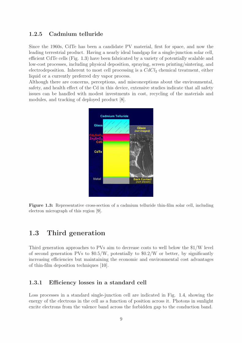
1.2.5 Cadmium telluride
Since the 1960s, CdTe has been a candidate PV material, first for space, and now theleading terrestrial product. Having a nearly ideal bandgap for a single-junction solar cell,efficient CdTe cells (Fig. 1.3) have been fabricated by a variety of potentially scalable andlow-cost processes, including physical deposition, spraying, screen printing/sintering, andelectrodeposition. Inherent to most cell processing is a CdCl2 chemical treatment, eitherliquid or a currently preferred dry vapor process.Although there are concerns, perceptions, and misconceptions about the environmental,safety, and health effect of the Cd in this device, extensive studies indicate that all safetyissues can be handled with modest investments in cost, recycling of the materials andmodules, and tracking of deployed product [8].
Figure 1.3: Representative cross-section of a cadmium telluride thin-film solar cell, includingelectron micrograph of this region [9].
1.3 Third generation
Third generation approaches to PVs aim to decrease costs to well below the $1/W levelof second generation PVs to $0.5/W, potentially to $0.2/W or better, by significantlyincreasing efficiencies but maintaining the economic and environmental cost advantagesof thin-film deposition techniques [10].
1.3.1 Efficiency losses in a standard cell
Loss processes in a standard single-junction cell are indicated in Fig. 1.4, showing theenergy of the electrons in the cell as a function of position across it. Photons in sunlightexcite electrons from the valence band across the forbidden gap to the conduction band.
9

A key fundamental loss process is process 1, whereby the photoexcited electron-hole pairquickly loses any energy it may have in excess of the bandgap. A low energy red photonis just as effective in terms of outcomes as a much higher energy blue photon. This lossprocess alone limits conversion efficiency of a cell to about 44% [11].Another important loss process is process 4, recombination of the photoexcited electron-hole pairs. This loss can be kept to a minimum by using a semiconductor material withappropriate properties, especially high lifetimes for the photogenerated carriers. This canbe ensured by eliminating all unnecessary defects.When open-circuited, the voltage of the ideal cell builds up so that the number of abovebandgap photons emitted as part of this voltage-enhanced radiation balances the numberin the incoming sunlight. At voltages below open-circuit, the number of emitted photonsis less, the difference between incoming and outgoing photons being made up by electronsflowing through cell terminals.In this way, Shockley and Queisser were able to show that the performance of standardcell was limited to 31% efficiency for an optimal cell with a bandgap of 1.3eV [12]. Thisis lower than the figure of 44% previously mentioned since the output voltage of the cellis less than the bandgap potential, with the difference accounted for by the voltage dropsat the contact and junction (loss processes 2 and 3 in Fig. 1.4).
Figure 1.4: Loss processes in a standard solar cell: (1) thermalisation loss; (2) and (3) junctionand contact voltage loss; (4) recombination loss [11].
1.3.2 Tandem cells
The key loss process 1 in Fig. 1.4 can be largely eliminated if the energy of the absorbedphoton is just a little higher than the bandgap of the cell material. This leads to theconcept of tandem cell, where multiple cells are used with different bandgaps, each cellconverting a narrow range of photon energies close to its bandgap as shown in Fig. 1.5(a).Fortunately, just stacking the cells with the highest bandgap cell uppermost as shown inFig. 1.5(b) automatically achieves the desired filtering. Limiting tandem cell performanceis quite good even with a relatively small number of cells in the stack, increasing fromthe single cell direct sunlight efficiency of 40.8 to 55.9, 63.8 and 68.8% as the number of
10
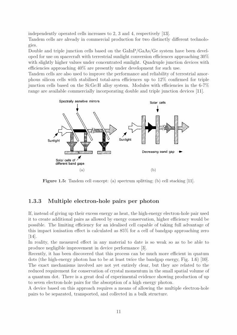
independently operated cells increases to 2, 3 and 4, respectively [13].Tandem cells are already in commercial production for two distinctly different technolo-gies.Double and triple junction cells based on the GaInP/GaAs/Ge system have been devel-oped for use on spacecraft with terrestrial sunlight conversion efficiences approaching 30%with slightly higher values under concentrated sunlight. Quadruple junction devices withefficiencies approaching 40% are presently under development for such use.Tandem cells are also used to improve the performance and reliability of terrestrial amor-phous silicon cells with stabilised total-area efficiences up to 12% confirmed for triplejunction cells based on the Si:Ge:H alloy system. Modules with efficiencies in the 6-7%range are available commercially incorporating double and triple junction devices [11].
(a) (b)
Figure 1.5: Tandem cell concept: (a) spectrum splitting; (b) cell stacking [11].
1.3.3 Multiple electron-hole pairs per photon
If, instead of giving up their excess energy as heat, the high-energy electron-hole pair usedit to create additional pairs as allowed by energy conservation, higher efficiency would bepossible. The limiting efficiency for an idealised cell capable of taking full advantage ofthis impact ionisation effect is calculated as 85% for a cell of bandgap approaching zero[14].In reality, the measured effect in any material to date is so weak so as to be able toproduce negligible improvement in device performance [3].Recently, it has been discovered that this process can be much more efficient in quatumdots (the high-energy photon has to be at least twice the bandgap energy, Fig. 1.6) [10].The exact mechanisms involved are not yet entirely clear, but they are related to thereduced requirement for conservation of crystal momentum in the small spatial volume ofa quantum dot. There is a great deal of experimental evidence showing production of upto seven electron-hole pairs for the absorption of a high energy photon.A device based on this approach requires a means of allowing the multiple electron-holepairs to be separated, transported, and collected in a bulk structure.
11

Figure 1.6: Multiple carrier generation in quantum dots: a high-energy photon is absorbed ata high energy level in the quantum dot, which then decays into two or more electron-hole pairsat the first confined energy level. Energy is conserved but momentum conservation is relaxed[10].
1.3.4 Hot carriers cells
Another option for increasing efficiencies is to allow absorption of a wide range of photonenergies, but then to collect the photogenerated carriers before they have a chance to ther-malize (see process 1 in Fig. 1.4). A hot-carrier solar cell is just such a device that offersthe possibility of very high efficiencies (the limiting efficiency is 65% for unconcentratedillumination) but with a structure that could be conceptually simple compared with othervery high efficiency PV devices.The concept underlying hot carrier solar cells is to slow the rate of photoexcited carriercooling, which is caused by phonon interaction in the lattice, to allow time for carriersto be collected while they are still at elevated energies. This allows higher voltages to beachieved by the cell. In addition to an absorber material that slows the rate of carrierrelaxation, a hot carrier cell must allow extraction of carriers from the device throughcontacts that accept only a very narrow range of energies (selective energy contacts), asshown in Fig. 1.7.
1.3.5 Multiband and impurity photovoltaic cells
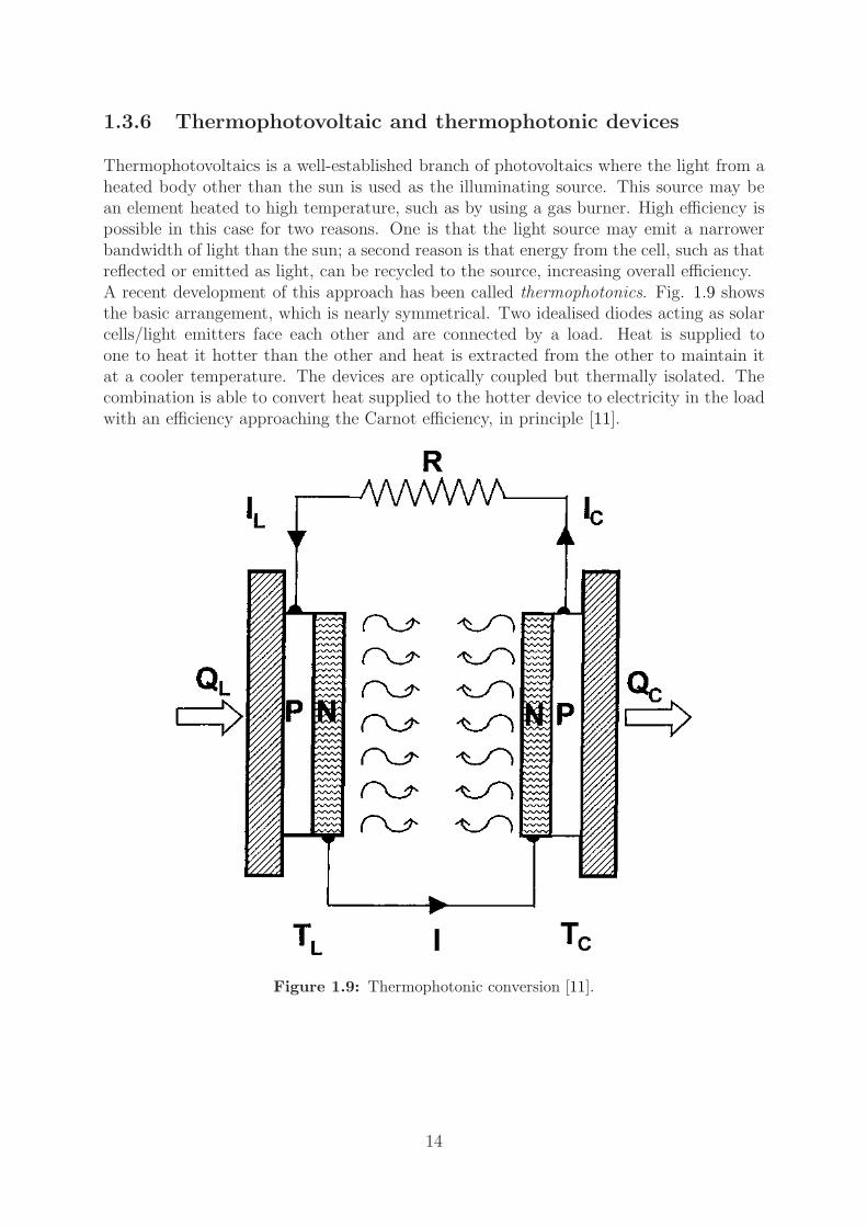
Standard cells rely on excitations between the valence and conduction band of a semicon-ductor. In 1997 Luque and Martı [15] have shown efficiency advantages if a third band,nominally an impurity band, is included in the analysis. This band can absorb photonswith sub-bandgap energies, in parallel with the normal operation of a single-bandgap cellleading to a limiting efficiency of 63.1%. These additional sub-bandgap absorber can ei-ther exist as a discrete energy level in an impurity PV (IPV) cell, or as a continuous bandof levels nonetheless isolated from the conduction and valence bands, the intermediateband solar cell (IBSC) shown in Fig. 1.8.
12
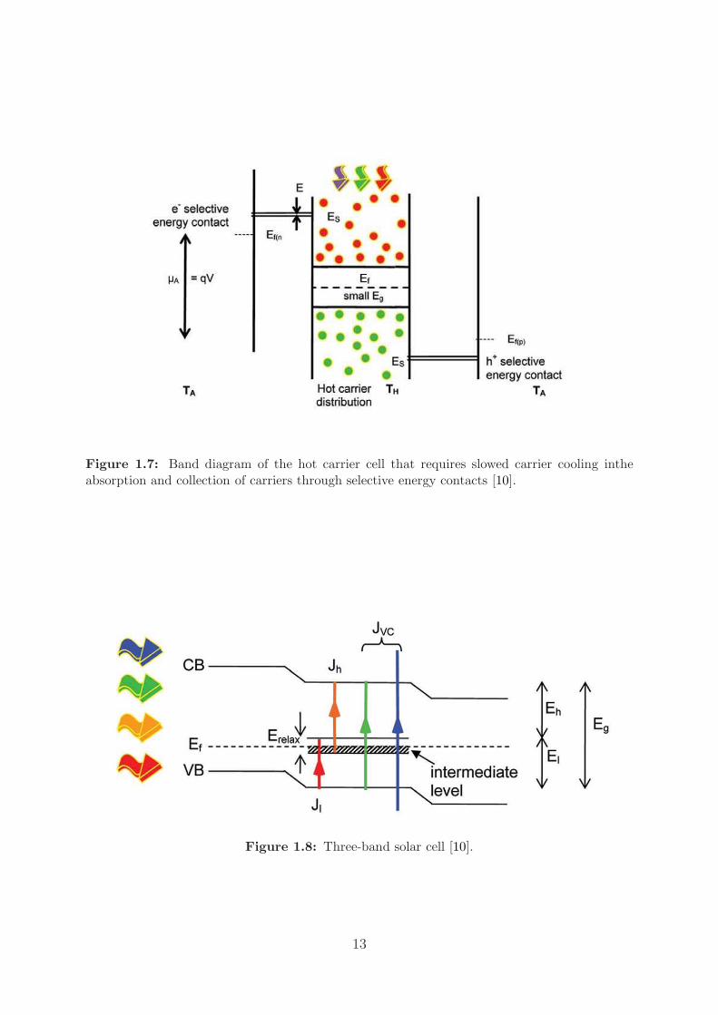
Figure 1.7: Band diagram of the hot carrier cell that requires slowed carrier cooling intheabsorption and collection of carriers through selective energy contacts [10].
Figure 1.8: Three-band solar cell [10].
13
1.3.6 Thermophotovoltaic and thermophotonic devices
Thermophotovoltaics is a well-established branch of photovoltaics where the light from aheated body other than the sun is used as the illuminating source. This source may bean element heated to high temperature, such as by using a gas burner. High efficiency ispossible in this case for two reasons. One is that the light source may emit a narrowerbandwidth of light than the sun; a second reason is that energy from the cell, such as thatreflected or emitted as light, can be recycled to the source, increasing overall efficiency.A recent development of this approach has been called thermophotonics. Fig. 1.9 showsthe basic arrangement, which is nearly symmetrical. Two idealised diodes acting as solarcells/light emitters face each other and are connected by a load. Heat is supplied toone to heat it hotter than the other and heat is extracted from the other to maintain itat a cooler temperature. The devices are optically coupled but thermally isolated. Thecombination is able to convert heat supplied to the hotter device to electricity in the loadwith an efficiency approaching the Carnot efficiency, in principle [11].
Figure 1.9: Thermophotonic conversion [11].
14


Chapter 2
Intermediate band solar cell
In this chapter the physics of intermediate band solar cell (IBSC) is presented. In sec-tion 2.1 and 2.2 an introduction and some preliminary concepts are given. In section2.3 a model for IBSC is shown while in section 2.4 the implementation of the cell bymeans of quantum dots (QD-IBSC) is pointed out. Finally, in section 2.5 some practicalconsiderations concerning this implementation are discussed.
2.1 Introduction
An intermediate band solar cell (IBSC) is a photovoltaic device conceived to exceed thelimiting efficiency of single-gap solar cells thanks to the exploitation of the electrical andoptical properties of intermediate-band (IB) material. This type of material takes itsname from the existence of an extra electronic band located in between what in ordinarysemiconductors constitutes its bandgap EG. The IB divides the bandgap EG into twoforbidden energy intervals (sub-bandgaps), EL and EH as drawn in Fig. 2.1(left). Forreasons that will become clearer shortly, it will also be required for this IB to be half-filledwith electrons.When light in this IB is absorbed, it has the potential to cause electronic transitions fromthe valence band (VB) to the IB, from the IB to the conduction band (CB) and, as inconventional semiconductors, also from the VB to the CB. These transitions are labelledas generation processes gIV , gCI and gCV , respectively, in Fig. 2.1(right). The inverse orrecombination processes are also labelled rIV , rCI and rCV , respectively.The absorption of photons takes the IB material out of equilibrium and causes the electronoccupation probability in each of the band to be described by Fermi-Dirac statistics withits own quasi-Fermi level. The temperature that corresponds to this statistic will be thelattice temperature, TC , and the quasi-Fermi level will be EFC, EFV and EFI dependingon the band we are referring to (CB, VB or IB).We admit three different quasi-Fermi levels exist, one for each of the bands, because weassume that the carrier recombination lifetimes between bands are much longer than thecarrier relaxation times within the bands. In particular, for proper IBSC operation, thequasi-Fermi level related to the IB, EFI , will be considered clamped at its equilibriumposition. The conditions for this hypothesis to hold are related to the excitation level and
17
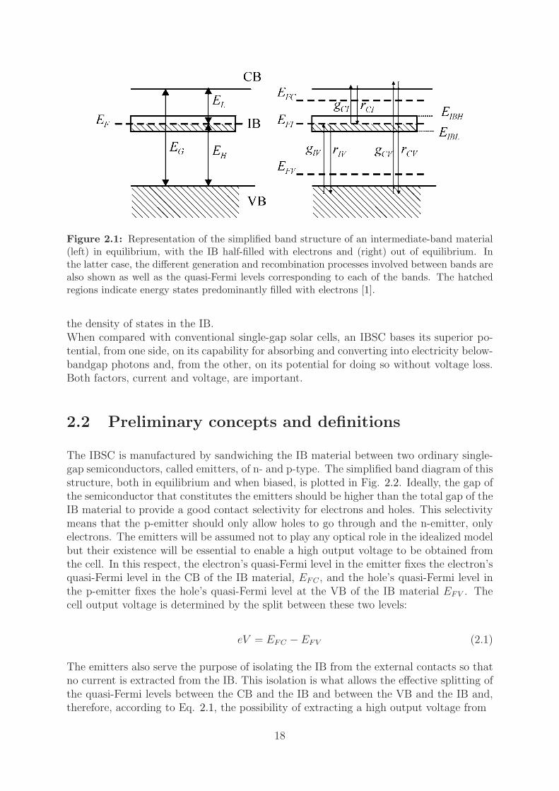
Figure 2.1: Representation of the simplified band structure of an intermediate-band material(left) in equilibrium, with the IB half-filled with electrons and (right) out of equilibrium. Inthe latter case, the different generation and recombination processes involved between bands arealso shown as well as the quasi-Fermi levels corresponding to each of the bands. The hatchedregions indicate energy states predominantly filled with electrons [1].
the density of states in the IB.When compared with conventional single-gap solar cells, an IBSC bases its superior po-tential, from one side, on its capability for absorbing and converting into electricity below-bandgap photons and, from the other, on its potential for doing so without voltage loss.Both factors, current and voltage, are important.
2.2 Preliminary concepts and definitions
The IBSC is manufactured by sandwiching the IB material between two ordinary single-gap semiconductors, called emitters, of n- and p-type. The simplified band diagram of thisstructure, both in equilibrium and when biased, is plotted in Fig. 2.2. Ideally, the gap ofthe semiconductor that constitutes the emitters should be higher than the total gap of theIB material to provide a good contact selectivity for electrons and holes. This selectivitymeans that the p-emitter should only allow holes to go through and the n-emitter, onlyelectrons. The emitters will be assumed not to play any optical role in the idealized modelbut their existence will be essential to enable a high output voltage to be obtained fromthe cell. In this respect, the electron’s quasi-Fermi level in the emitter fixes the electron’squasi-Fermi level in the CB of the IB material, EFC , and the hole’s quasi-Fermi level inthe p-emitter fixes the hole’s quasi-Fermi level at the VB of the IB material EFV . Thecell output voltage is determined by the split between these two levels:
eV = EFC − EFV (2.1)
The emitters also serve the purpose of isolating the IB from the external contacts so thatno current is extracted from the IB. This isolation is what allows the effective splitting ofthe quasi-Fermi levels between the CB and the IB and between the VB and the IB and,therefore, according to Eq. 2.1, the possibility of extracting a high output voltage from
18

Figure 2.2: From top to bottom. Basic structure of an intermediate band solar cell. Simplifiedbandgap diagram in equilibrium. Simplified bandgap diagram under illumination and forwardbias [16].
the cell.Different absorption coefficients associated with each of the absorption processes that cantake place in the IB material can be defined. These coefficients are labelled αIV , αCIand αCV so as to describe the strength of the absorption of photons that cause electrontransition from the VB to the IB, from the IB to the CB and from the VB to the CB,respectively. Aiming for the maximum efficiency, these processes have to be reversible,which requires, from one side, that the recombination to be exclusively radiative in natureand, from the other, that the absorption coefficients do not overlap in energy. That theabsorption coefficients do not overlap in energy means that for a given photon energy, E,only one of the three absorption coefficients is non-zero or, in other words, that only oneof the transitions described is possible. Hence, we shall assume that
αCI 6= 0 if EL < E < EH (2.2)
αIV 6= 0 if EH < E < EG (2.3)
αCV 6= 0 if EG < E. (2.4)
19

Now it is also understood why the Fermi level has been fixed within the IB. It is both toprovide enough empty states in the IB to accomodate the electrons pumped from the VBand also to supply enough electrons to be pumped to the CB. In non-equilibrium condi-tions, this Fermi level turns into three quasi-Fermi levels for describing the concentrationof electrons in the three bands. Moreover, the quasi-Fermi level in the IB is assumed tobe clamped at its equilibrium position when the cell becomes excited. This is in order toprevent the IB from becoming fully filled or emptied of electrons, which would change theabsorption properties of the material as a function of the biasing.The absorption-recombination processes can be symbolically represented by the followingchemical reactions:
hνCI ↔ eC + hI (2.5)
hνIV ↔ eI + hV (2.6)
hνCV ↔ eC + hV (2.7)
Equalling the chemical potential of the elements involved in Eq. 2.5, 2.6 and 2.7, we statethat
µCI = EFC − EFI (2.8)
µIV = EFI −EFV (2.9)
µCV = EFC − EFV (2.10)
where µXY is the chemical potential of the photons that are in equilibrium with thecreation and annihilation of electron-hole pairs between band X and Y. The spectraldensity of these photons is given by b(ǫ, µXY , TC) where
b(ǫ, µ, T ) =2
h3c2ǫ2
exp ǫ−µkT
− 1(2.11)
In Eq. 2.11, ǫ is the photon energy and T the temperature. The parameters h, c andk have their usual meaning: Planck’s constant, speed of light in vacuum and Boltzmannconstant respectively.There is a limitation to the quasi-Fermi level split that can be tolerated and is related tothe IB width. If the upper and lower energy levels of the IB are designed by EIBH andEIBL, then we must have µCI < EC − EIBH and µIV < EIBL − EV , where EC and EVare the energy limits of the CB and VB respectively, otherwise stimulated emission wouldtake place. For maximum sunlight concentration (46050 suns), it has been estimated [1]that this bandwidth limit is in the range of 100 meV while, for 1 sun operation, this limitenlarges up to 700 meV. Conversely, there is a potential limitation for the narrownessof the IB bandwidth. It is known that as a band narrows, the carrier mobility tends todecrease. However, because no current is extracted from the IB, no carrier transport inthe IB is required either as long as we keep in the model idealizations that assume thatthe generation and recombination processes are not dependent on position all over the IB
20

material.With respect to Eq. 2.11, it will be useful to define the following auxiliary functions:
NS(ǫL, ǫH) = π∫ ǫH
ǫL
b(ǫ, 0, TS)dǫ (2.12)
N(ǫL, ǫH , µXY , T ) = π∫ ǫH
ǫL
b(ǫ, µXY , T )dǫ (2.13)
The purpose of Eq. 2.12 is to enable the number of photons that a solar cell absorbs,when the photon spectral density is assumed to be that of a black body at temperatureTS and the maximum concentration is used. Similarly Eq. 2.13 is intended to be a toolto describe the number of photons emitted from the cell.
2.3 Intermediate band solar cell: model
In the ideal model [15], the IBSC is considered to operate in its radiative limit. Inaddition, ideal photon selectivity is considered so that a photon with energy E can onlybe absorbed by a unique type of transition. Complete photon absorption is assumed(absorptivity equal to unity).The electron current density, JC extracted from the n+ contact can be obtained from usingdetailed balance arguments with respect to the conduction band. Hence, this currentis stated to be given as the difference between the number of photons from the sunthat are absorbed per unit area causing transition ending in he CB (JLC/e), and thosephotons that are emitted outside of the cell (JOC(V )/e) and originated in recombinationmechanisms that started in the CB. For this purpose, the sun will be taken as a blackbody at TS = 6000K, and the cell at a temperature TC = 300K and a maximum lightconcentration will be assumed. Therefore, in mathematical terms, we write
JC = JLC − JOC(V ) (2.14)
where
JLC = eNS(EG,∞) + eNS(EL, EH) (2.15)
JOC(V ) = eN(EG,∞, eV, TC) + eN(EL, EH , µCI , TC) (2.16)
Similarly, the hole current density JV , extracted from the VB is given by:
JV = JLV − JOV (V ) (2.17)
where
21

JLV = eNS(EG,∞) + eNS(EH , EG) (2.18)
JOV (V ) = eN(EG,∞, eV, TC) + eN(EH , EG, eV − µCI , TC) (2.19)
The current density-voltage (J-V ) characteristic of the IBSC is obtained by solving si-multaneously the set of equations:
J = JC = JV (2.20)
eV = µCV = µCI + µIV (2.21)
Eq. 2.14 and 2.17 can be represented in equivalent circuit form by the circuit shown inFig. 2.3, where the voltage between nodes X and Y corresponds to the quasi-Fermi levelsplit µXY .The efficiency of the IBSC, as a function of the gaps EL and EG (or EH), is then triviallyobtained by maximizing the output power from the cell, P = J(V )V , and dividing theresult by the imput power, Pin = σT 4
S . In a further optimization process, EG can be op-timized as a function of EL. The results are shown in Fig. 2.4. The maximum efficiencyis EL = 0.71eV and EH = 1.24eV (i.e. EG = 1.95eV). This limiting efficiency is superiorto that of single-gap solar cells (40.7%) and that of two solar cells connected in series(55.4%) as also shown in Fig. 2.4.
Figure 2.3: Equivalent circuit for an ideal IBSC. Under normal conditions (non-degeneracy),the currents JXY follow the Shockley’s diode equation quite accurately [17].
22
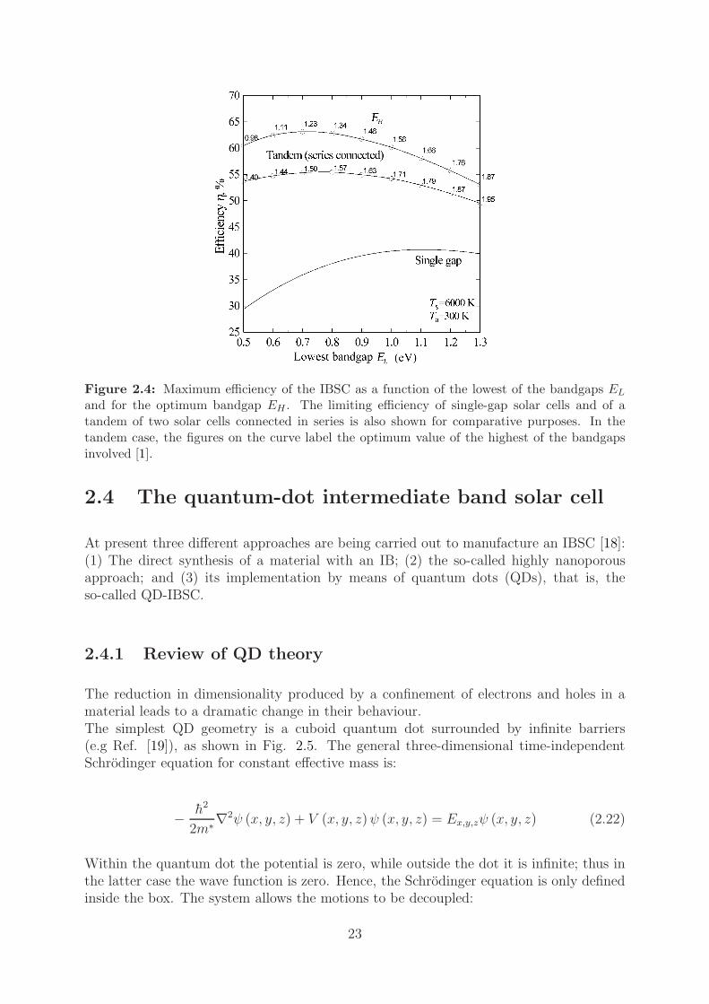
Figure 2.4: Maximum efficiency of the IBSC as a function of the lowest of the bandgaps EL
and for the optimum bandgap EH . The limiting efficiency of single-gap solar cells and of atandem of two solar cells connected in series is also shown for comparative purposes. In thetandem case, the figures on the curve label the optimum value of the highest of the bandgapsinvolved [1].
2.4 The quantum-dot intermediate band solar cell
At present three different approaches are being carried out to manufacture an IBSC [18]:(1) The direct synthesis of a material with an IB; (2) the so-called highly nanoporousapproach; and (3) its implementation by means of quantum dots (QDs), that is, theso-called QD-IBSC.
2.4.1 Review of QD theory
The reduction in dimensionality produced by a confinement of electrons and holes in amaterial leads to a dramatic change in their behaviour.The simplest QD geometry is a cuboid quantum dot surrounded by infinite barriers(e.g Ref. [19]), as shown in Fig. 2.5. The general three-dimensional time-independentSchrodinger equation for constant effective mass is:
− h2
2m∗∇2ψ (x, y, z) + V (x, y, z)ψ (x, y, z) = Ex,y,zψ (x, y, z) (2.22)
Within the quantum dot the potential is zero, while outside the dot it is infinite; thus inthe latter case the wave function is zero. Hence, the Schrodinger equation is only definedinside the box. The system allows the motions to be decoupled:
23
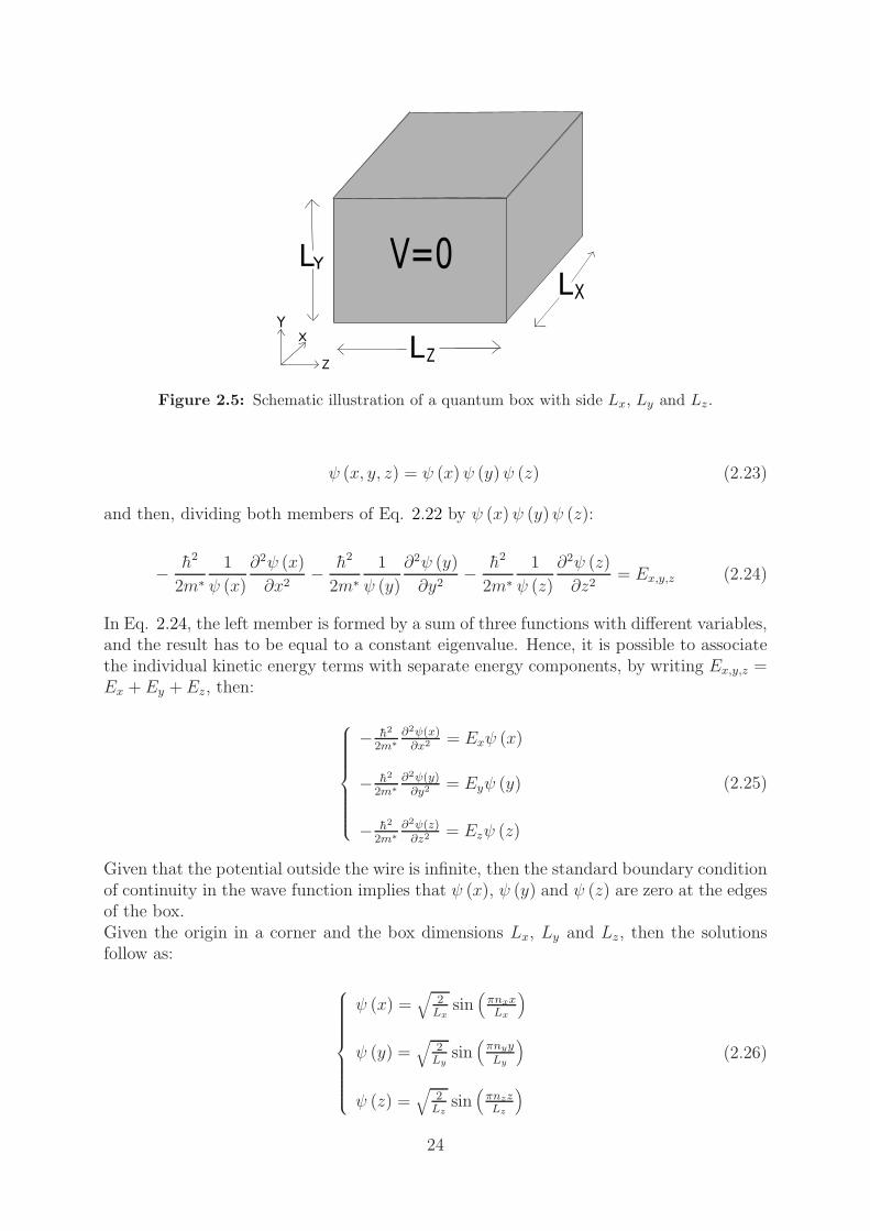
Figure 2.5: Schematic illustration of a quantum box with side Lx, Ly and Lz.
ψ (x, y, z) = ψ (x)ψ (y)ψ (z) (2.23)
and then, dividing both members of Eq. 2.22 by ψ (x)ψ (y)ψ (z):
− h2
2m∗
1
ψ (x)
∂2ψ (x)
∂x2− h2
2m∗
1
ψ (y)
∂2ψ (y)
∂y2− h2
2m∗
1
ψ (z)
∂2ψ (z)
∂z2= Ex,y,z (2.24)
In Eq. 2.24, the left member is formed by a sum of three functions with different variables,and the result has to be equal to a constant eigenvalue. Hence, it is possible to associatethe individual kinetic energy terms with separate energy components, by writing Ex,y,z =Ex + Ey + Ez, then:
− h2
2m∗
∂2ψ(x)∂x2 = Exψ (x)
− h2
2m∗
∂2ψ(y)∂y2
= Eyψ (y)
− h2
2m∗
∂2ψ(z)∂z2
= Ezψ (z)
(2.25)
Given that the potential outside the wire is infinite, then the standard boundary conditionof continuity in the wave function implies that ψ (x), ψ (y) and ψ (z) are zero at the edgesof the box.Given the origin in a corner and the box dimensions Lx, Ly and Lz, then the solutionsfollow as:
ψ (x) =√
2Lx
sin(
πnxxLx
)
ψ (y) =√
2Ly
sin(
πnyy
Ly
)
ψ (z) =√
2Lz
sin(
πnzzLz
)
(2.26)
24
which give the components of energy as:
Ex = h2π2n2x
2m∗L2x
Ey =h2π2n2
y
2m∗L2y
Ez = h2π2n2z
2m∗L2z
(2.27)
Thus, the global wavefunction ψ (x, y, z) and the total energy due to confinement Ex,y,z,are:
ψ (x, y, z) = 2√
2√LxLyLz
sin(
πnxxLx
)
sin(
πnyy
Ly
)
sin(
πnzzLz
)
Ex,y,z = h2π2
2m∗
(
n2x
L2x
+n2
y
L2y
+ n2z
L2z
)
(2.28)
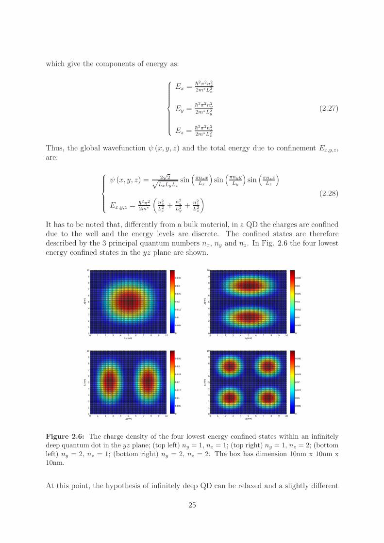
It has to be noted that, differently from a bulk material, in a QD the charges are confineddue to the well and the energy levels are discrete. The confined states are thereforedescribed by the 3 principal quantum numbers nx, ny and nz. In Fig. 2.6 the four lowestenergy confined states in the yz plane are shown.
0 1 2 3 4 5 6 7 8 9 100
1
2
3
4
5
6
7
8
9
10
Ly (nm)
Lz(n
m)
0
0.005
0.01
0.015
0.02
0.025
0.03
0.035
0 1 2 3 4 5 6 7 8 9 100
1
2
3
4
5
6
7
8
9
10
Ly(nm)
Lz(n
m)
0
0.005
0.01
0.015
0.02
0.025
0.03
0.035
0 1 2 3 4 5 6 7 8 9 100
1
2
3
4
5
6
7
8
9
10
Ly(nm)
Lz(n
m)
0
0.005
0.01
0.015
0.02
0.025
0.03
0.035
0 1 2 3 4 5 6 7 8 9 100
1
2
3
4
5
6
7
8
9
10
Ly(nm)
Lz(n
m)
0
0.005
0.01
0.015
0.02
0.025
0.03
0.035
Figure 2.6: The charge density of the four lowest energy confined states within an infinitelydeep quantum dot in the yz plane; (top left) ny = 1, nz = 1; (top right) ny = 1, nz = 2; (bottomleft) ny = 2, nz = 1; (bottom right) ny = 2, nz = 2. The box has dimension 10nm x 10nm x10nm.
At this point, the hypothesis of infinitely deep QD can be relaxed and a slightly different
25

system can be analysed.Assume to have QD surrounded by a finite potential well. Eq. 2.28 are no longer exacteigenfunctions and eigenvalues of Schrodinger’s equation for the problem. The boundaryconditions have to be changed from the quantum box with infinite potential barrier toa more realistic QD with a finite well. This implies the wavefunction not to be zero atthe boundary and a finite charge density appears outside the dot. Nevertheless, Eq. 2.28can be considered a good approximation for the lower energy states if the height of thebarrier is sufficiently high. A picture of a one dimensional well is shown in Fig. 2.7; asnx incresases to more than 3, the energy becomes higher than V0; the related chargesdo not experience the barrier anymore and they are free to move along the x-axis (thewavefunctions are not localized anymore).The similarities between the energy levels in a QD and those in an atom have led to thealternative definition of artificial atom for these 0-dimensional quantum structures.
Figure 2.7: Energy levels of a QD surrounded by a potential V0. The x direction and the lower3 energy levels are shown.
2.4.2 From discrete levels to bands
When quantum nanostructures, such as QDs, are arranged in super-lattice arrays, mini-bands will be produced. In such structures, the QDs play a role similar to that of atomsin real crystal. Tomic et al. [20] have presented a theoretical study on the electronicstructure of a QD array made by InAs/GaAs.The calculation were based on a 8-band k·p Hamiltonian. In the model periodic 3D array,each QD was a truncated pyramid with a base length of b = 12 nm and height h = 6nm, on top of a one monolayer wetting layer (Fig. 2.8). The periodicity of the array wascontrolled by the dimensions of the embedding box. In the x and y directions they keptperiodicity constant Lx = Ly = 20 nm, while the periodicity along z-axes was changed inthe range from 1 to 10 nm.
26
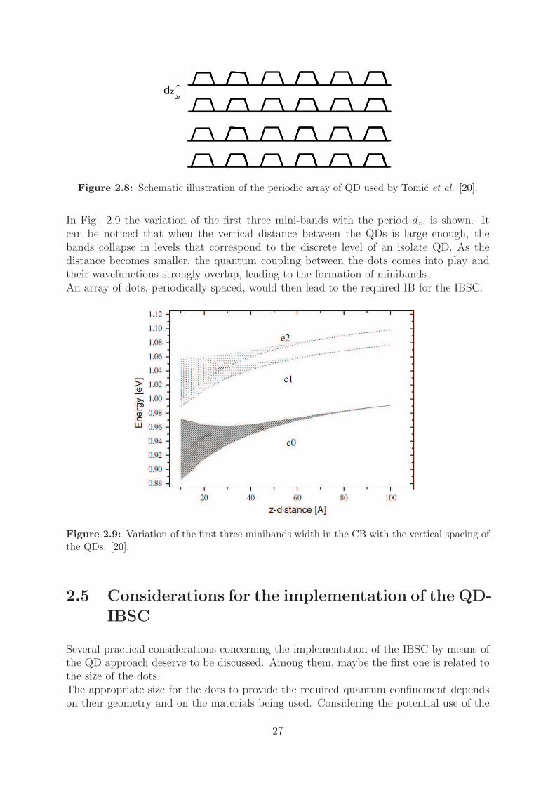
Figure 2.8: Schematic illustration of the periodic array of QD used by Tomic et al. [20].
In Fig. 2.9 the variation of the first three mini-bands with the period dz, is shown. Itcan be noticed that when the vertical distance between the QDs is large enough, thebands collapse in levels that correspond to the discrete level of an isolate QD. As thedistance becomes smaller, the quantum coupling between the dots comes into play andtheir wavefunctions strongly overlap, leading to the formation of minibands.An array of dots, periodically spaced, would then lead to the required IB for the IBSC.
Figure 2.9: Variation of the first three minibands width in the CB with the vertical spacing ofthe QDs. [20].
2.5 Considerations for the implementation of the QD-
IBSC
Several practical considerations concerning the implementation of the IBSC by means ofthe QD approach deserve to be discussed. Among them, maybe the first one is related tothe size of the dots.The appropriate size for the dots to provide the required quantum confinement dependson their geometry and on the materials being used. Considering the potential use of the
27

III-V semiconductors for manufacturing the array, assuming spherical dots and using theeffective mass approximation, it has been estimated [1] that the radius of the dots shouldbe in the range of 39 A. In principle, such dot sizes are achievable by using MBE self-assembly growth techniques such as the Stranski-Krastanov mode, as discussed in chapter3.Another topic of interest is the density of the dots (number of the dots per unit volume).In this respect, several aspects point to the fact that this should be as high as possiblewith some limitations briefly discussed later.In theory, although the dots are very well spaced, the IB structure would still hold aslong as the dots are identical and located in a perfect periodic scheme. However, as thedots become more and more spaced, there is more risk for a minimal perturbation in theperiodicity causing the electron wavefunctions to transit from being delocalized (as wouldbe the case when they form part of a proper band structure) to being localized. This isthe case in which the IB has lost its band structure to return to coming a mere collectionof energy levels. Therefore, from this perspective, the density of dots should be as highas possible.A benefit derived from a high density of dots is simply related to the increment in thestrength of absorption of light by the dots. If the density of dots is very low, lightabsorption by the dots will be weak and, in order to compensate for it, the use of a highvolume of QD material or, alternatively, the use of light trapping techniques, is necessary.Another benefit derived from a high dot density is related to the clamping of the IB quasi-Fermi level at its equilibrium position. In order for this clamping to occur, the density ofstates in the IB has to be sufficiently high. The specific number depends on the injectionlevel at which the cell is planned to be operated. When using QDs, the density of states isgiven by twice the density of dots (if dots with one confined level are manufactured), thefactor two arising from taking the electron spin degeneracy into account. In this respect,it has been determined that a density of dots in the order of 1017cm−3 would be necessaryto clamp the quasi-Fermi level within kT for cell operation in the range of 1000 suns [1].A third advantage comes from the fact that as the dots become more closely spaced, theIB broadens. This fact tends to increase carrier mobility in the IB and, although thismobility is not required in an idealized structure in which the IB would be uniformlyexcited by the generation-recombination mechanisms, it could be required, in practise,to facilitate carrier redistribution through the IB from the places where they are moreintensely generated to the regions where they are more intensely recombined.There is, however a limit to this IB broadening, the most obvious of which being to preventthe IB from mixing with the CB or VB. Another limit comes from the prevention of theappearance of stimulated emission effects. In spite of this, it seems that the centres ofthe dots could be safely located at a distance of 100 A[21] without any of these problemsappearing.
28


Chapter 3
Growth of InAs/GaAs quantum dotsby MBE
In this chapter the growth of InAs/GaAs QDs by MBE is discussed. In section 3.1 theStranski-Krastanov growth mode is presented. Afterwards, the physics behind the processis pointed out: in section 3.2 the first step of deposition is shown (2D phase), while insection 3.3 the 2D-3D transition is explained (formation of QDs). Finally, in section 3.4the capping process is examined.
3.1 Stranski-Krastanov growth mode
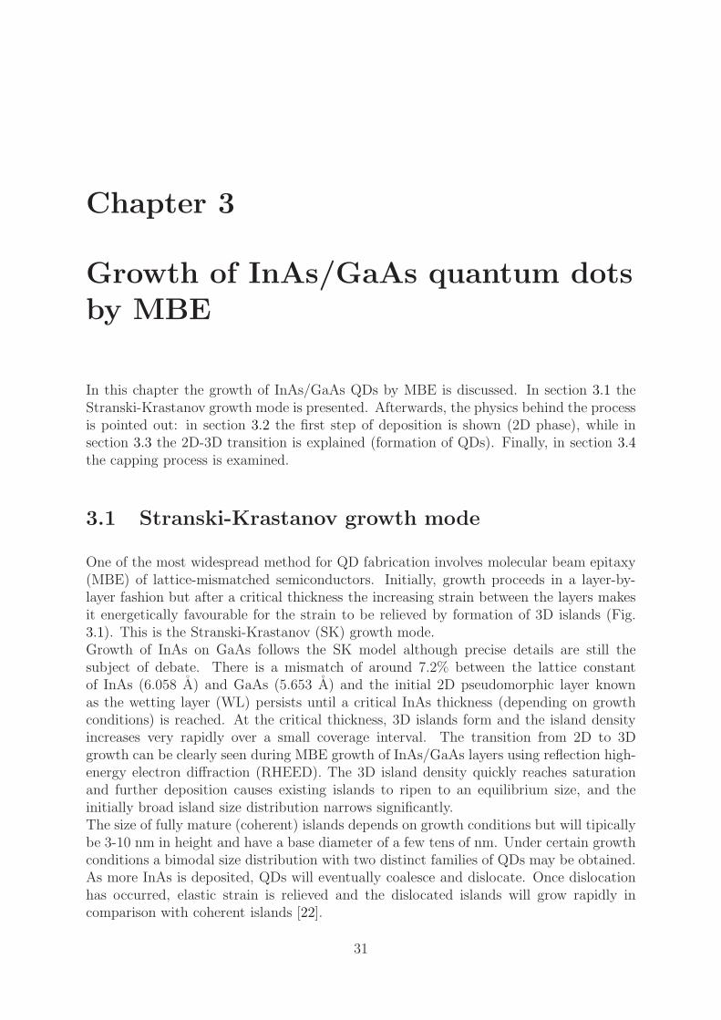
One of the most widespread method for QD fabrication involves molecular beam epitaxy(MBE) of lattice-mismatched semiconductors. Initially, growth proceeds in a layer-by-layer fashion but after a critical thickness the increasing strain between the layers makesit energetically favourable for the strain to be relieved by formation of 3D islands (Fig.3.1). This is the Stranski-Krastanov (SK) growth mode.Growth of InAs on GaAs follows the SK model although precise details are still thesubject of debate. There is a mismatch of around 7.2% between the lattice constantof InAs (6.058 A) and GaAs (5.653 A) and the initial 2D pseudomorphic layer knownas the wetting layer (WL) persists until a critical InAs thickness (depending on growthconditions) is reached. At the critical thickness, 3D islands form and the island densityincreases very rapidly over a small coverage interval. The transition from 2D to 3Dgrowth can be clearly seen during MBE growth of InAs/GaAs layers using reflection high-energy electron diffraction (RHEED). The 3D island density quickly reaches saturationand further deposition causes existing islands to ripen to an equilibrium size, and theinitially broad island size distribution narrows significantly.The size of fully mature (coherent) islands depends on growth conditions but will tipicallybe 3-10 nm in height and have a base diameter of a few tens of nm. Under certain growthconditions a bimodal size distribution with two distinct families of QDs may be obtained.As more InAs is deposited, QDs will eventually coalesce and dislocate. Once dislocationhas occurred, elastic strain is relieved and the dislocated islands will grow rapidly incomparison with coherent islands [22].
31

Figure 3.1: Schematic illustration of Stranski-Krastanov growth; a) strained wetting layer, b)formation of a quantum dot.
Although heteroepitaxy of InAs/GaAs(001) is of SK type, such a transition has a morecomplex evolution from its initial stage. Specific issues, which differ from the conventionalSK growth are, for instance, the following [23]:
(i) the 2D WL is an InGaAs alloy having a precise composition at the transition [24];
(ii) the 2D to 3D transition, at the critical thickness, occours within 0.2 ML of InAsdeposition, by the sudden nucleation of 1010 − 1011 cm−2 QDs which are coherentand strained;
(iii) InAs QDs include some Ga at their bases, whose amount depends on growth condi-tions;
(iv) the nucleated 3D volume is far larger than that being deposited in the narrow cov-erage range where nucleation is completed.
Other details of InAs/GaAs heteroepitaxy concern thermodynamic and kinetic aspects ofthe growth, such as the dependence of the critical thickness on substrate temperature andIn flux.
32

3.2 The 2D phase: wetting layer and critical thick-
ness
During the deposition process of InAs on GaAs substrate, the InAs-GaAs interface is notmerely abrupt and the first monolayer deposited is far from being pure InAs. Surface
segregation1 and In-Ga exchange affect the composition of the growth film.Cullis et al [24] propose a model (called WCNH) for the SK growth of strained semi-conductor heterostructures which focuses on the WL composition and, in particular, onthe strain dependence of the critical thickness, in InxGa1−xAs/GaAs systems, as a conse-quence on In segregation in the WL. The model considers exchange of the group-III speciesbetween the top two layers during growth so that the surface layer exhibits a very sub-stantial deviation from the deposition flux concentration. If a relatively diluite (x=0.25)alloy is deposited, Fig. 3.2 shows the way in which the In concentration is predicted bythe theory to evolve within the growing flat layer. It is evident that segregation of In tothe surface enhances the In concentration in the surface monolayer rapidly above that ofthe deposition flux so that, for only ∼ 1 nm of layer growth, the surface In concentrationis already above 40%. It is then important to determine the variation in predicted surfaceIn concentration as a function of deposition flux composition. This is presented in Fig.3.3 (left panel) where the curves show this quantity for deposition fluxes containing from5% to 100%.The WCNH mechanism proposes that a critical surface concentration of In (and associatedstrain) must build up before the SK-islanding transition take place. Since a depositionflux of 25% In is approximately the lowest that will induce the SK transition, it is possibleto identify the corresponding critical surface In concentration from the associated curvein Fig. 3.2: the critical concentration would be predicted to be 80-85% In in the surfacelayer (saturation concentration). For any particular deposition flux, it is predicted thatthe SK transition will take place after the surface In concentration rises to this criticallevel. Thus the islanding transition points for layers grown over the complete range ofdeposition fluxes can be estimated from plots of the type given in Fig. 3.3 (left panel), sothat is possible to estimate the critical transition thickness of the initial flat wetting layeras a function of deposited In concentration. This then gives the continuous ”theoretical”curve in Fig. 3.3 (right panel), which extends from 2.5 nm thickness for a depositionflux of 25% In to 0.3 nm thickness for InAs deposition. It is evident that the thoreticallyand experimentally derived curves exhibit exactly the same form and are displaced fromone another by no more than 0.1-0.5 nm, depending upon In flux concentration. Thenear coincidence of the curves lends strong support for the importance of segregation indetermining the SK 2D-3D transition point, as proposed in the WCNH mechanism.For deposition of InAs on GaAs, an initial delay in the increase of the surface In concen-tration to 100% [curve (g) in Fig. 3.3 (left panel)] results from the exchange of In atomswith Ga atoms in the GaAs surface. In this latter case, partial completion of the secondmonolayer is required before the surface In concentration and associated strain becomehigh enough to trigger the SK 3D-islanding transition.
1The term surface segregation refers to the enrichment of one or more component of the mixture inthe surface region, relative to bulk composition, through the perturbation of the bonding mechanism [25]
33

Figure 3.2: Composition variations in the near-surface InxGa1−xAs monolayers (shown bybars), driven by In segregation to the surface (In concentration variation in the surface monolayeris tracked by the solid line). Deposition flux is 25% In and different total-growth thicknessesare: (a) 3 monolayers, (b) 5 monolayers, and (c) 10 monolayers [24].
Figure 3.3: Left panel: composition variations in the surface monolayer, driven by In segre-gation to the surface, for deposition fluxes with (a) 5% In, (b) 10% In, (c) 25% In, (d) 35%In, (e) 55% In, (f) 80% In, and (g) 100% In. Right panel: variation in the flat-layer thicknessfor the islanding transition as a function of In concentration in the deposition flux: measuredvalues given as data points and theoretically predicted values based upon the WCNH mechanismpresented as a continuous curve [23].
34

3.3 The 3D phase: evolution of the surface morphol-
ogy during 2D-3D transition
Close to the critical thickness, the morphology of the InAs/GaAs(001) interface becomequite rich, as shown in Fig. 3.4. The images reveal an involved morphology of the WLcomprising 2D islands 1 ML high, and large terraces one step high. Kinetic instabilities ofthe growth due to anisotropy of diffusion and the extra barrier for down-hopping at stepedges, give rise to the stepped texture of the WL, which strongly influences the in-planeposition of dots; in fact, most of them nucleate at step edges. 2D islands appear in allsamples at about 1.4 ML and vanish when the massive nucleation of large QDs is takingplace. The first small QDs are recognizable for coverage as high as 1.45 ML, whereas athigher InAs deposits the formation and subsequent number increase of large QDs can beseen. Small QDs nucleate preferentially at the upper-step edges of 2D islands and terracesby reason of a favourable strain condition at these sites. Placidi et al. [23] demonstratethat they are not simple precursors of large QDs but the process involves a more complexkinetic mechanism.
Figure 3.4: 1x1 µm2 AFM topographies for continuous growth (CG) and growth interruption(GI) samples. The images show the WL at 1.42 ML, free from 3D features, the first small QDsat 1.48 ML and the occurrence of large QDs at 1.54 ML for the GI sample and at 1.60 ML forthe other. Adapeted from [23].
The number density evolution of both small and large QDs for the GI (growth interrup-tion) sample is shown in Fig. 3.5. The number of the small QDs begins to increase at1.45 ML and maximizes at 1.57 ML. Starting from 1.52 ML, the number of the large QDsincreases gradually, then, between 1.57 and 1.61 ML, it undergoes a sudden rise, changingvalue by an order of magnitude. At higher coverages (>1.8 ML) the density rise is muchslower.One of the puzzling aspects of the self-assembled QDs is that the nucleated 3D volumeis far larger than that being deposited in the narrow coverage range where the entirenucleation process is completed. This phenomen could be a consequence of the erosion
of step edge surrounding dots. If the total dot volume was plotted as a function of thedeposited InAs (not shown), two regions with different slopes would be distinguished [23].In the range 1.6-1.8 ML, the dependence of the dot volume on coverage is linear, with
35

Figure 3.5: Number density dependence on InAs coverage of small and large QDs [23].
slope Ft ∼ 4F0 for all the samples, where F0 is the slope of the straight line representingthe volume being deposited by the impinging InAs flux. Above 1.8 ML, the volumeincreases at the same rate F0 as the coverage. It is worth underlining that the volumebehaviour just described is clear evidence of large surface mass transport from the 2Dto the 3D phase at the very initial stage of the transition. This can be quantified as anextra coverage of approximately ∆t = 0.9 ML for the CG (continuous growth) and the GIsamples. Such mass transfer ends above 1.8 ML, above which the volume increases solelyat the expense of the incoming flux.The ensuing discussion concerns the microscopic origin of such excess volume.While at the beginning of nucleation all dots nucleate on step edge, at 1.9 ML ∼ 60% ofthem are found below it. This is consistent with the fact that dots first nucleate at theupper side of the step edge, then, as a result of step erosion, they are located at the lowerside of the step. Therefore, in addition to surface segregation and substrate intermixing,a relevant fraction of the dot volume comes from step erosion: not enough, however, toaccount for all the 3D volume in excess. A further contribution can be attribuited to thepresence of floating In adatoms at the very beginning of nucleation.
3.4 Overgrowth: capping process
Freestanding islands are hardly ever employed but are instead covered by a capping layer(typically of the same material as the substrate) that preserves them from the externalenvironment and suppresses nonradiative recombination through surface states also at theupper interface.A fundamental aspect that has attracted substantial attention is that the deposition ofthe capping layer might be, and very often is, far from being harmless for the 3D is-lands [26–29]. In fact, the capping procedure itself is a lattice mismatched heteroepitaxialprocess and is therefore associated with strain release, segregation, faceting, intermixing,strain-enhanced diffusion, etc. These phenomena take place at the island surface and canstrongly modify the QD morphology and composition. Since the optical and electronicproperties of QDs strongly depend on their size, shape, and stoichiometry, a detailed mi-croscopic understanding of the capping process that ultimately allows a tailoring of the
36

optoelectronic characteristics becomes essential.Strong differences in the capping process have been found, depending on the size of theQDs, but here we focuses on the model for small QDs [29] (suitable for IBSC application),shown in Fig. 3.6.Exceeding the critical thickness, the InAs layer can relax strain energy by forming the QDstructure [Fig. 3.6(a)]. The relaxation occours mostly at the apex of the QD, while thebase remains almost at the GaAs lattice parameter due to the pseudomorphic interface.Thus, the local lattice parameter (LLP) at the QD apex is close to the value of bulk InAs,decreasing slightly toward its base edges and corners. The strain energy of this freestand-ing, uncapped QD amounts to 40%-60% of the energy of the same one capped and thuscompressed into the lattice of the surrounding GaAs matrix. During capping the amountof relaxed strain energy in principle has to be reinvested. In the directly surroundingGaAs matrix, the LLP becomes slightly lower than the lattice constant of bulk GaAs.Only far away from the QDs the GaAs capping material adopts its bulk lattice constant.The strain energy situation for the GaAs material strikinig directly the QD is most unfa-vorable. Thereby, it diffuses toward the sides of the QD where it finds more preferentialsticking positions, dragging the InAs from the apex along with it [Fig. 3.6(b) and 3.6(c),lateral arrows]. Thus, the apex gets removed, and both materials intermix and stick tothe sides of the QD, increasing the steepness of the side facets. On the one hand, thisprocess leads to a global strain energy reduction compared with the situation of a cappedpyramid. On the other hand, the LLP on top of the QD slightly decreases since the dis-tance to the base becomes smaller. During further capping [Fig. 3.6(d)] the GaAs layer ishigher above the WL than above the QD, and the QD itself gets covered first at its sideand finally at its center. This is the result of a competition between the strain energy andthe step energies of a rough growth surface. Finally, the QD gets completely capped andthe GaAs growth surface flattens again [Fig. 3.6(e)]. Segregation also occours at the WLafter deposition of GaAs [Fig. 3.6(b) and 3.6(d), vertical arrows].
Figure 3.6: Schematic model for the capping process of the QD structure: (a) the situationbefore capping and [(b)-(e)] after deposition of increasingly thick capping layers [29].
37


Chapter 4
Experimental
The goal of this thesis is to study the dependence of the QDs density and sizes on thegrowth parameters, for intermediate band solar cell application.Self-organized InAs/GaAs QDs structures were grown on n-type GaAs(001) substrate bya Veeco Gen-II solid-source molecular beam epitaxy (MBE) system. The grown layersconsisted of a 200 nm GaAs buffer layer grown at 590◦C. Afterwards growth was inter-rupted and the substrate temperature reduced to the value chosen for QD growth. TheInAs QDs were capped by 10 nm GaAs grown at the same substrate temperature as theQDs. Then the growth was interrupted again and the substrate temperature raised to590◦C for further 40 nm GaAs deposition. Another QD layer was repeated after the GaAsbarrier layer, at the same growth conditions as the buried one, for AFM examinations.The basic structure of the samples is also shown in Fig. 4.1.
Figure 4.1: Schematic view of the samples structure. Although the structures are qualitativelythe same, they were grown at different temperatures (ranging from 360◦C to 480◦C), withdifferent InAs thicknesses (from 2.0ML to 2.8ML), with different Arsenic fluxes and at differentrates.
39
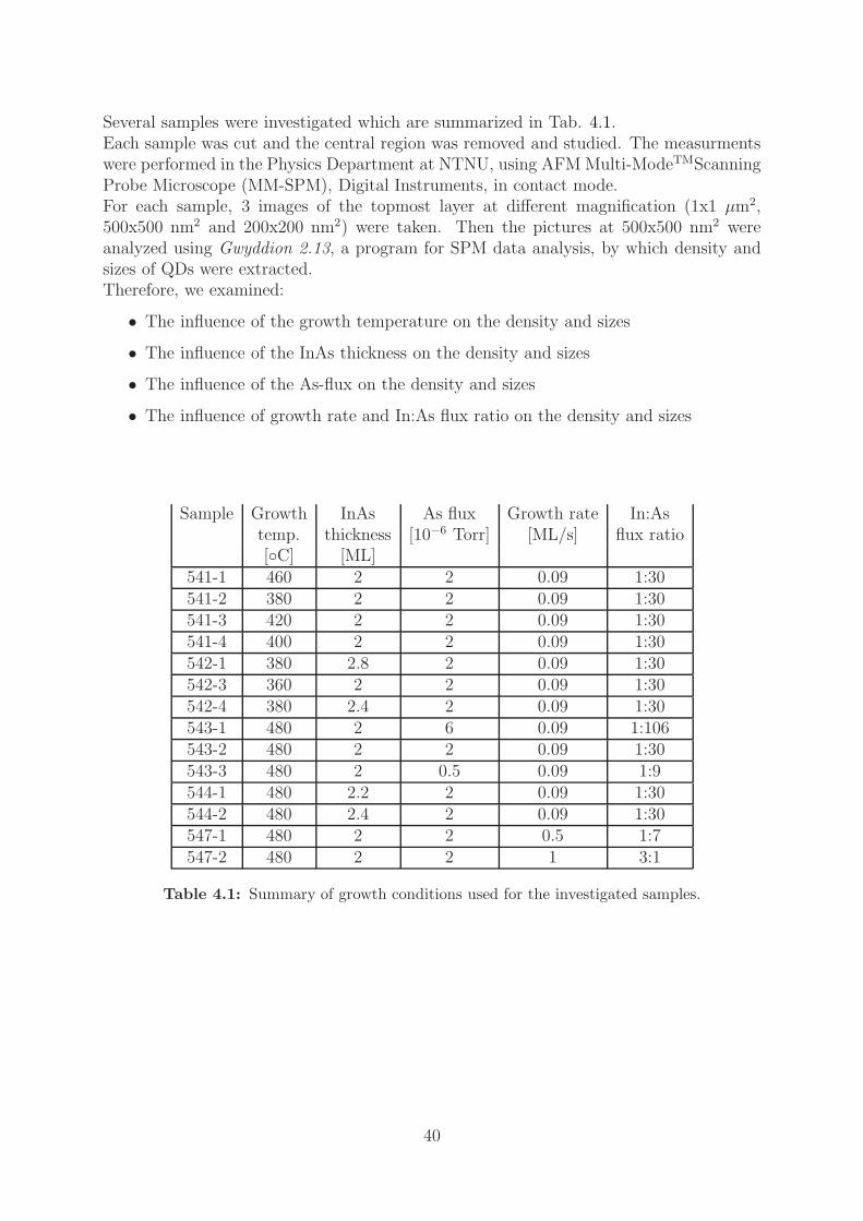
Several samples were investigated which are summarized in Tab. 4.1.Each sample was cut and the central region was removed and studied. The measurmentswere performed in the Physics Department at NTNU, using AFM Multi-ModeTMScanningProbe Microscope (MM-SPM), Digital Instruments, in contact mode.For each sample, 3 images of the topmost layer at different magnification (1x1 µm2,500x500 nm2 and 200x200 nm2) were taken. Then the pictures at 500x500 nm2 wereanalyzed using Gwyddion 2.13, a program for SPM data analysis, by which density andsizes of QDs were extracted.Therefore, we examined:
• The influence of the growth temperature on the density and sizes
• The influence of the InAs thickness on the density and sizes
• The influence of the As-flux on the density and sizes
• The influence of growth rate and In:As flux ratio on the density and sizes
Sample Growth InAs As flux Growth rate In:Astemp. thickness [10−6 Torr] [ML/s] flux ratio[◦C] [ML]
541-1 460 2 2 0.09 1:30541-2 380 2 2 0.09 1:30541-3 420 2 2 0.09 1:30541-4 400 2 2 0.09 1:30542-1 380 2.8 2 0.09 1:30542-3 360 2 2 0.09 1:30542-4 380 2.4 2 0.09 1:30543-1 480 2 6 0.09 1:106543-2 480 2 2 0.09 1:30543-3 480 2 0.5 0.09 1:9544-1 480 2.2 2 0.09 1:30544-2 480 2.4 2 0.09 1:30547-1 480 2 2 0.5 1:7547-2 480 2 2 1 3:1
Table 4.1: Summary of growth conditions used for the investigated samples.
40


Chapter 5
Image processing using Gwyddion
In this chapter, a brief description of Gwyddion is given in section 5.1. Moreover in section5.2 the main sources of errors are discussed and in section 5.3 different routines for imageprocessing are presented. The results of the processing are shown in section 5.4, while thefinal routine and the estimated errors are stated in section 5.5.
5.1 Introduction
Gwyddion is a modular program for SPM data analysis. Primarily it is supposed tobe used for analysis of height fields obtained by means of scanning probe microscopytechniques (AFM, MFM, STM, NSOM), but generally it can be used for any other heightfield analysis or image analysis.It is a free-source and open-source program available on internet [30]; it is also possibleto find a comprehensive user guide [31].The useful information that we want to extract from an AFM image are:
• The density of QDs
• The mean diameter of QDs
• The mean height of QDs
• The FWHM of diameters’ distribution
• The FWHM of heights’ distribution
By Gwyddion it is possible to extract a raw data file containing all the information weneed. Processing the raw data by, e.g. MATLAB R©, allows us to get the final results.
5.2 Sources of error
An AFM image will typically be affected by several sources of error (horizontal scars, lines,noise, etc.), that compromise the quality of the picture and the validity of the results. It
43
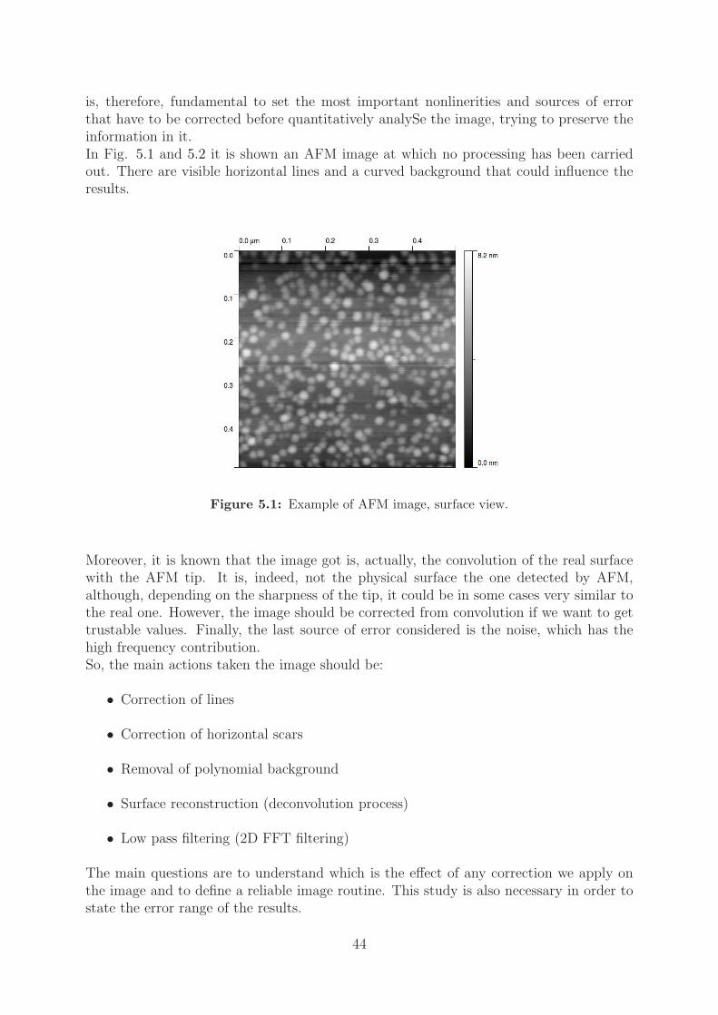
is, therefore, fundamental to set the most important nonlinerities and sources of errorthat have to be corrected before quantitatively analySe the image, trying to preserve theinformation in it.In Fig. 5.1 and 5.2 it is shown an AFM image at which no processing has been carriedout. There are visible horizontal lines and a curved background that could influence theresults.
Figure 5.1: Example of AFM image, surface view.
Moreover, it is known that the image got is, actually, the convolution of the real surfacewith the AFM tip. It is, indeed, not the physical surface the one detected by AFM,although, depending on the sharpness of the tip, it could be in some cases very similar tothe real one. However, the image should be corrected from convolution if we want to gettrustable values. Finally, the last source of error considered is the noise, which has thehigh frequency contribution.So, the main actions taken the image should be:
• Correction of lines
• Correction of horizontal scars
• Removal of polynomial background
• Surface reconstruction (deconvolution process)
• Low pass filtering (2D FFT filtering)
The main questions are to understand which is the effect of any correction we apply onthe image and to define a reliable image routine. This study is also necessary in order tostate the error range of the results.
44
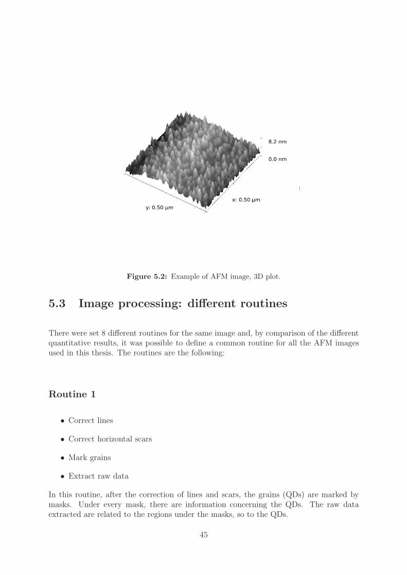
Figure 5.2: Example of AFM image, 3D plot.
5.3 Image processing: different routines
There were set 8 different routines for the same image and, by comparison of the differentquantitative results, it was possible to define a common routine for all the AFM imagesused in this thesis. The routines are the following:
Routine 1
• Correct lines
• Correct horizontal scars
• Mark grains
• Extract raw data
In this routine, after the correction of lines and scars, the grains (QDs) are marked bymasks. Under every mask, there are information concerning the QDs. The raw dataextracted are related to the regions under the masks, so to the QDs.
45

Routine 2
• Correct lines
• Correct horizontal scars
• Remove polynomial background (horizontal polynom degree 3rd and vertical poly-nom degree 3rd )
• Mark grains
• Extract raw data
In this routine, the background is removed using a 3rd degree polynom as fitting function.The entire image is used for fitting.
Routine 3
• Correct lines
• Correct horizontal scars
• Mark grains
• Remove polynomial background (horizontal polynom degree 3rd and vertical poly-nom degree 3rd, excluding region under mask )
• Extract raw data
In this routine, the background is removed using a 3rd degree polynom as fitting functionbut it is not exploited the entire image for fitting. The QDs are excluded from theoperation and preserved from the previous operation.
Routine 4
• Correct lines
• Correct horizontal scars
• Mark grains
• Remove polynomial background (horizontal polynom degree 3rd and vertical poly-nom degree 3rd, excluding region under mask )
• Blind tip estimation (run partial)
• Surface reconstruction
• Mark grains in the deconvoluted image
• Extract raw data
46

In this routine, the background is removed using a 3rd degree polynom as fitting functionbut it is not exploited the entire image for fitting. The QDs are excluded from theoperation and preserved from the previous operation. Afterwards, a blind tip estimationis performed and the deconvolution is carried out using as tip the estimated one.
Routine 5
• Correct lines
• Correct horizontal scars
• Remove polynomial background (horizontal polynom degree 3rd and vertical poly-nom degree 3rd)
• Blind tip estimation (run partial)
• Surface reconstruction
• Mark grains in the deconvoluted image
• Extract raw data
In this routine, the background is removed using a 3rd degree polynom as fitting function.The entire image is used for fitting. Afterwards, a blind tip estimation is performed andthe deconvolution is carried out using as tip the estimated one.
Routine 6
• Correct lines
• Correct horizontal scars
• Mark grains
• Remove polynomial background (horizontal polynom degree 3rd and vertical poly-nom degree 3rd, excluding region under mask )
• Low pass filtering (2D FFT filtering)
• Mark grains in the filtered image
• Extract raw data
In this routine, the background is removed using a 3rd degree polynom as fitting functionbut it is not exploited the entire image for fitting. The QDs are excluded from theoperation and preserved from the previous operation. Afterwards, low pass filtering iscarried out.
Routine 7
• Correct lines
47

• Correct horizontal scars
• Mark grains
• Remove polynomial background (horizontal polynom degree 1st and vertical poly-nom degree 1st, excluding region under mask)
• Extract raw data
In this routine, the background is removed using a 1st degree polynom as fitting functionbut it is not exploited the entire image for fitting. The QDs are excluded from theoperation and preserved from the previous operation.
Routine 8
• Correct lines
• Correct horizontal scars
• Mark grains
• Remove polynomial background (horizontal polynom degree 2nd and vertical poly-nom degree 2nd, excluding region under mask )
• Extract raw data
In this routine, the background is removed using a 2nd degree polynom as fitting functionbut it is not exploited the entire image for fitting. The QDs are excluded from the oper-ation and preserved from the previous operation.
In all the routines is assumed that correcting lines and horizontal scars does not affectsignificantly the final results.Comparing routine 1,2 and 3 is, therefore, possible to analyze the effect of backgroundsubtraction including and excluding the regions under the masks; comparing routine 7, 8and 3 the different degrees of polynomial background subtraction are studied. Moreover,looking at routine 2 and 5 as weel as routine 3 and 4, the effect of surface reconstructionis evaluated. Finally routine 3 and 6 give information about low pass filtering.
5.4 Image processing: results
5.4.1 Background subtraction
In Fig. 5.3 and 5.4 the effect of the background subtraction including and excluding theregion under the masks is shown, considering the distribution of diameters and heights ofthe QDs.Removing polynomial background including the grains leads to a marked reduction (∼1nm)in mean diameter, while the mean height does not seem to be affected. It suggests thatremoving polynomial background without ”protecting” the QD from this action affects
48

the contour of the QD, a sensitive part of the image that strongly feels the effect of sub-traction. Moreover the normal distributions fitting of routine 1 and 3 are overlapped, asexpected.Fig. 5.5 and 5.6, instead, show the comparison between the 1st, the 2nd and the 3rd orderof polynomial background subtracted from the original image, excluding the QDs.Undoubtedly the three routines lead to an identical result, both for diameters and heights.
15 20 25 300
50
Diameter [nm]
Cou
nts
[arb
.un.
] Routine 1
15 20 25 300
50
Diameter [nm]
Cou
nts
[arb
.un.
] Routine 2
15 20 25 300
50
Diameter [nm]
Cou
nts
[arb
.un.
] Routine 3
15 20 25 300
10
20
30
40
50
60
Diameter [nm]
Cou
nts
[arb
.un.
]
Normal Distribution Fitting
Routine 1
Routine 2
Routine 3
Figure 5.3: Histograms and normal distributions fitting of diameters for routine 1, 2 and 3.The normal distributions of routine 1 and 3 are overlapped.
0 1 2 3 4 50
50
100
Height [nm]
Cou
nts
[arb
.un.
] Routine 1
0 1 2 3 4 50
50
100
Height [nm]
Cou
nts
[arb
.un.
] Routine 2
0 1 2 3 4 50
50
100
Height [nm]
Cou
nts
[arb
.un.
] Routine 3
0 1 2 3 4 50
10
20
30
40
50
60
70
80
90
100
110
Height [nm]
Cou
nts
[arb
.un.
]
Normal Distribution Fitting
Routine 1Routine 2Routine 3
Figure 5.4: Histograms and normal distributions fitting of heights for routine 1, 2 and 3. Thenormal distributions of routine 1 and 3 are overlapped.
49

15 20 25 300
50
Diameter [nm]
Cou
nts
[arb
.un.
] Routine 7
15 20 25 300
50
Diameter [nm]
Cou
nts
[arb
.un.
] Routine 8
15 20 25 300
50
Diameter [nm]
Cou
nts
[arb
.un.
] Routine 3
15 20 25 300
5
10
15
20
25
30
35
40
45
50
55
Diameter [nm]
Cou
nts
[arb
.un.
]
Normal Distribution Fitting
Routine 7Routine 8Routine 3
Figure 5.5: Histograms and normal distributions fitting of diameters for routine 7, 8 and 3.
0 1 2 3 4 50
50
100
Height [nm]
Cou
nts
[arb
.un.
] Routine 7
0 1 2 3 4 50
50
100
Height [nm]
Cou
nts
[arb
.un.
] Routine 8
0 1 2 3 4 50
50
100
Height [nm]
Cou
nts
[arb
.un.
] Routine 3
0 1 2 3 4 50
10
20
30
40
50
60
70
80
90
100
Height [nm]
Cou
nts
[arb
.un.
]
Normal Distribution Fitting
Routine 7Routine 8Routine 3
Figure 5.6: Histograms and normal distributions fitting of heights for routine 7, 8 and 3.
In conclusion, background subtraction likely reduces the heights and the diamaters of theQDs if they are not excluded from this action. It can therefore slightly modify the sizesof the nanostructers imaged. Moreover. background subtraction, regardless which degreepolynom used, if performed excluding the grains does not affect the original data. It isjust a way to flatten the background.
50
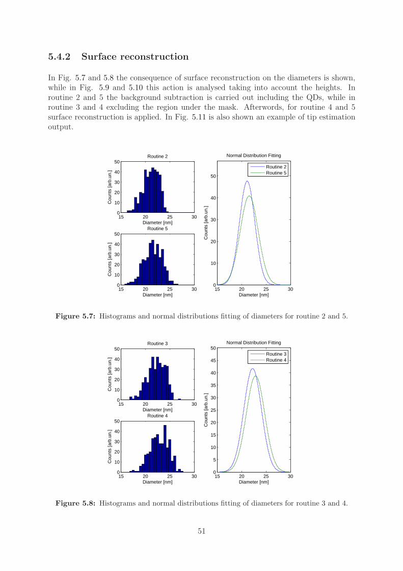
5.4.2 Surface reconstruction
In Fig. 5.7 and 5.8 the consequence of surface reconstruction on the diameters is shown,while in Fig. 5.9 and 5.10 this action is analysed taking into account the heights. Inroutine 2 and 5 the background subtraction is carried out including the QDs, while inroutine 3 and 4 excluding the region under the mask. Afterwords, for routine 4 and 5surface reconstruction is applied. In Fig. 5.11 is also shown an example of tip estimationoutput.
15 20 25 300
10
20
30
40
50
Diameter [nm]
Cou
nts
[arb
.un.
]
Routine 2
15 20 25 300
10
20
30
40
50
Diameter [nm]
Cou
nts
[arb
.un.
]
Routine 5
15 20 25 300
10
20
30
40
50
Diameter [nm]
Cou
nts
[arb
.un.
]
Normal Distribution Fitting
Routine 2Routine 5
Figure 5.7: Histograms and normal distributions fitting of diameters for routine 2 and 5.
15 20 25 300
10
20
30
40
50
Diameter [nm]
Cou
nts
[arb
.un.
]
Routine 3
15 20 25 300
10
20
30
40
50
Diameter [nm]
Cou
nts
[arb
.un.
]
Routine 4
15 20 25 300
5
10
15
20
25
30
35
40
45
50
Diameter [nm]
Cou
nts
[arb
.un.
]
Normal Distribution Fitting
Routine 3Routine 4
Figure 5.8: Histograms and normal distributions fitting of diameters for routine 3 and 4.
51

0 1 2 3 4 50
20
40
60
80
100
120
Height [nm]
Cou
nts
[arb
.un.
]
Routine 2
0 1 2 3 4 50
20
40
60
80
100
120
Height [nm]
Cou
nts
[arb
.un.
]
Routine 5
0 1 2 3 40
20
40
60
80
100
120
Height [nm]C
ount
s [a
rb.u
n.]
Normal Distribution Fitting
Routine 2Routine 5
Figure 5.9: Histograms and normal distributions fitting of heights for routine 2 and 5.
0 1 2 3 4 50
20
40
60
80
100
120
Height [nm]
Cou
nts
[arb
.un.
]
Routine 3
0 1 2 3 4 50
20
40
60
80
100
120
Height [nm]
Cou
nts
[arb
.un.
]
Routine 4
0 1 2 3 40
20
40
60
80
100
120
Height [nm]
Cou
nts
[arb
.un.
]
Normal Distribution Fitting
Routine 3Routine 4
Figure 5.10: Histograms and normal distributions fitting of heights for routine 3 and 4.
The most remarkable effects are the slighlty decrease in mean height (∼4.5%) and thenarrowing of the normal distribution fitting for heights (∼20.5%). The diameters, in-stead, have the opposite trend; the mean increases of about 1.8-2.6% and the normaldistributions broaden. The amount of this broadening is quite different looking at thetwo different routines involved in surface reconstruction, routine 4 and 5. The latter, thatinvolves background subtraction including QDs, leads to a FWHM of normal distributionlarger of 17% than the one in routine 2, while for the former, that excludes QDs from thesubtraction, the broadening is smaller (∼5%).
52

Then, surface reconstruction contributes to reduce the mean height and narrow its normaldistribution, while regarding the diameters, the mean value is larger and the distributionis broader.
Figure 5.11: Example of blind tip estimation output, 3D view.
5.4.3 Low pass filtering
The last comparison that was analyzed is between routine 3 and 6, in order to check theeffect of low pass filtering as shown in Fig. 5.12 and 5.13.
15 20 25 300
10
20
30
40
50
Diameter [nm]
Cou
nts
[arb
.un.
]
Routine 3
15 20 25 300
10
20
30
40
50
Diameter [nm]
Cou
nts
[arb
.un.
]
Routine 6
15 20 25 300
5
10
15
20
25
30
35
40
45
50
Diameter [nm]
Cou
nts
[arb
.un.
]
Normal Distribution Fitting
Routine 3Routine 6
Figure 5.12: Histograms and normal distributions fitting of diamteres for routine 3 and 6.
53

0 1 2 3 4 50
20
40
60
80
100
Height [nm]
Cou
nts
[arb
.un.
]
Routine 3
0 1 2 3 4 50
20
40
60
80
100
Height [nm]
Cou
nts
[arb
.un.
]
Routine 6
0 1 2 3 40
10
20
30
40
50
60
70
80
90
100
Height [nm]C
ount
s [a
rb.u
n.]
Normal Distribution Fitting
Routine 3Routine 6
Figure 5.13: Histograms and normal distributions fitting of heights for routine 3 and 6.
Low pass filtering the image leads to a reduction of either the mean height (∼4.5%) andmean diameter (∼2.7%), keeping FWHMs unchanged.This operation is helpful and logically necessary because the noise in the image has mainlyan high frequency contribution.
5.5 Image processing: final routine
The evaluation of the image processing showed in the previous sections has been necessaryin order to understand and quantify the effect that every single step in the processing willhave on the original image. The final routine chosen for the analysis of all the samplesgrown by MBE is a suitable and logically ordered sequence of operation that can beperformed by Gwyddion.The final routine is the following:
• Correct lines
• Correct horizontal scars
• Mark grains
• Remove polynomial background (horizontal polynom degree 3rd and vertical poly-nom degree 3rd, excluding region under mask )
• Blind tip estimation, run partial
• Surface reconstruction
• Low pass filtering (2D FFT filtering)
• Mark grains in the deconvoluted and filtered image
54

• Extract raw data
Finally, the estimated errors for density, mean diameter and mean height are 3.5%, 7.5%and 4.5% respectively.
55


Chapter 6
Results and discussion
In this chapter the results of this study are shown and discussed. In section 6.1, the resultsare presented, while the dependence of sizes and density of QDs on growth temperature,InAs thickness, As flux, growth rate and In:As flux ratio are discussed in section 6.2, 6.3,6.4, 6.5 and 6.6, respectively.
6.1 Presentation of results
The 14 samples grown by MBE are presented in chapter 4, Tab. 4.1. The central partof the samples was cut and AFM images were taken at different magnification (1x1 µm2,500x500 nm2 and 200x200 nm2).The best images are shown in Appendix A.Then, the 500x500 nm2 images were analyzed using Gwyddion 2.13, by means of the im-age processing routine described in chapter 5. The raw data extracted after the processingwere elaborated using MATLAB R©’s codes attached in Appendix B.In Tab. 6.1 and 6.2 the results are displayed. In Tab. 6.1, the densities and the amount ofmaterial incorporated in the QDs, expressed in equivalent monolayer (MLeq), are shown,while in Tab. 6.2, the average heights and diamaters as well as the corresponding FWHMsare pointed out. The zeros in both tables express the impossibilty of getting any quan-titative results from the images. This is due not because the routine or the program isunable to do that, but simply because the samples theirselves do not show any properQDs in the surface, as it will be discussed later in the chapter.
57

Sample Density MLeq[1011 cm−2] [ML]
541-1 1,85 0,52541-2 0 0541-3 2,74 0,41541-4 0 0542-1 0 0542-3 0 0542-4 0 0543-1 1,44 1,71543-2 1,46 1,1543-3 1,48 1,13544-1 1,71 1,05544-2 1,56 1,56547-1 1.97 0,6547-2 1,79 0,7
Table 6.1: Results: the densities and the amount of material incorporated in the QDs, expressedin equivalent monolayer (MLeq), are shown .
Sample Mean FWHM Mean FWHMHeight Height Diameter Diameter[nm] [nm] [nm] [nm]
541-1 1.1 0,71 22,1 8,48541-2 0 0 0 0541-3 0,8 0,59 17,3 6,59541-4 0 0 0 0542-1 0 0 0 0542-3 0 0 0 0542-4 0 0 0 0543-1 3,2 1,88 24,6 8,01543-2 2,2 1,18 23,1 6,83543-3 2 0,94 21,2 4544-1 1,8 0,94 22,8 8,24544-2 2,7 2,12 24,6 8,24547-1 1,1 0,71 21,1 5,56547-2 1,4 1,06 22,9 6,83
Table 6.2: Results: the mean heights and diameters as well as the corresponding FWHMs areshown.
58

6.2 Dependence on growth temperature
Fig. 6.1 shows 1x1 µm2 AFM images of samples growth at temperatures ranging from360 to 480◦C (2.0 ML InAs, 2x10⁻⁶ Torr As flux and 0.09 ML/s growth rate).The only sample that clearly displayes QDs is the one at 480◦C, while for the other tem-peratures, just some coalescence is visible.
Figure 6.1: 1x1 µm2 top view AFM images of 2.0 ML InAs, 2x10⁻⁶ Torr As flux and 0.09ML/s growth rate, grown at different temperatures.
59

In order to have a quantitative description of the surfaces, height profiles of samples weretaken, as shown in Fig. 6.2. To make the comparison easier, where possible, coalescentdot was included in the profile.Up to 400◦C, the profiles show mounds around 0.5 nm high that made any quantitativeanalysis impossible. These is a feature of rough surfaces that can hardly be classified asQDs.Proper QDs show up at 420◦C, 460◦C and definitely at 480◦C.
0 100 200 300 4000
0.5
1
1.5
2
2.5
3
X [nm]
Z [n
m]
360◦C
0 100 200 300 4000
0.5
1
1.5
2
2.5
3
X [nm]
Z [n
m]
380◦C
0 100 200 300 4000
1
2
3
4
5
6
X [nm]
Z [n
m]
400◦C
0 100 200 300 4000
0.5
1
1.5
2
2.5
3
X [nm]
Z [n
m]
420◦C
0 100 200 300 4000
1
2
3
4
5
6
7
X [nm]
Z [n
m]
460◦C
0 100 200 300 4000
1
2
3
4
X [nm]
Z [n
m]
480◦C
Figure 6.2: Surface profiles of samples of 2.0 ML InAs, 2x10⁻⁶ Torr As flux and 0.09 ML/sgrowth rate, grown at different temperatures.
In Fig. 6.3, the density, mean diameters and mean heights are plotted.Once the QDs are formed, increasing the temperature leads to a decrease in density, whilethe mean diameter increases. These trends are in agreement with several previous studies
60
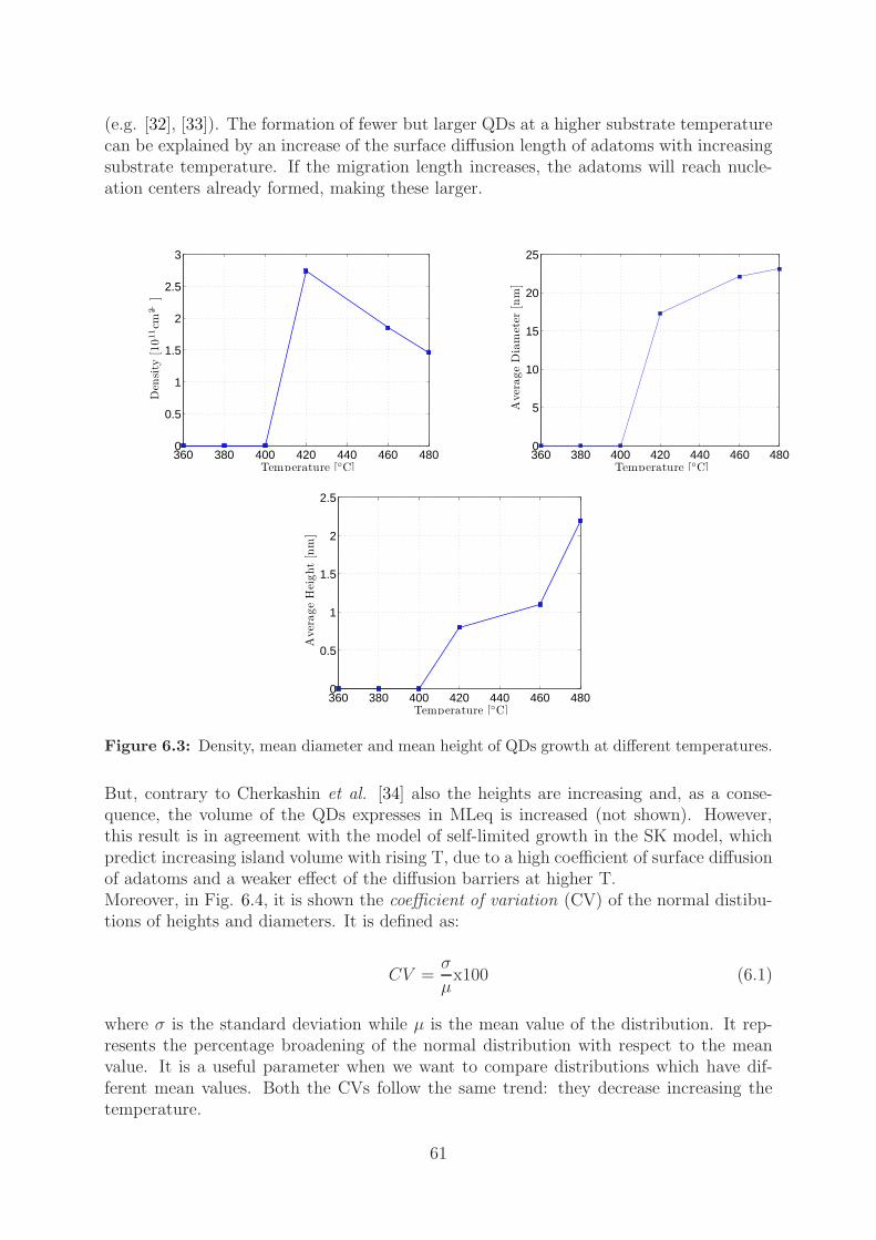
(e.g. [32], [33]). The formation of fewer but larger QDs at a higher substrate temperaturecan be explained by an increase of the surface diffusion length of adatoms with increasingsubstrate temperature. If the migration length increases, the adatoms will reach nucle-ation centers already formed, making these larger.
360 380 400 420 440 460 4800
0.5
1
1.5
2
2.5
3
Temperature [◦C]
Den
sity
[10
11cm
−2]
360 380 400 420 440 460 4800
5
10
15
20
25
Temperature [◦C]
Aver
age
Dia
met
er[n
m]
360 380 400 420 440 460 4800
0.5
1
1.5
2
2.5
Temperature [◦C]
Aver
age
Hei
ght
[nm
]
Figure 6.3: Density, mean diameter and mean height of QDs growth at different temperatures.
But, contrary to Cherkashin et al. [34] also the heights are increasing and, as a conse-quence, the volume of the QDs expresses in MLeq is increased (not shown). However,this result is in agreement with the model of self-limited growth in the SK model, whichpredict increasing island volume with rising T, due to a high coefficient of surface diffusionof adatoms and a weaker effect of the diffusion barriers at higher T.Moreover, in Fig. 6.4, it is shown the coefficient of variation (CV) of the normal distibu-tions of heights and diameters. It is defined as:
CV =σ
µx100 (6.1)
where σ is the standard deviation while µ is the mean value of the distribution. It rep-resents the percentage broadening of the normal distribution with respect to the meanvalue. It is a useful parameter when we want to compare distributions which have dif-ferent mean values. Both the CVs follow the same trend: they decrease increasing thetemperature.
61

Therefore, although at lower temperature the QDs density is higher, the very small sizes ofthe nanostructures might be not so effective for creating the intermediate band in the solarcell because the quantum confinement required could be hardly manifested. In addition,the higher CVs make 420◦C not a suitable temperature for growing IBSC, keeping theother growth parameters constant, because the distribution of size should be as narrow aspossible. From this perspective, 480◦C could be suitable for that purpose, having a goodcompromise between density and broadening and likely also the quantum confinementrequired.
360 380 400 420 440 460 4800
5
10
15
20
25
30
35
Temperature [◦C]
Coe
ffici
ent
ofVar
iation
[%]
CV Diameter CV Height
Figure 6.4: Coefficient of variation of diameters and heights at various growth temperatures.
6.3 Dependence on InAs thickness
In Fig. 6.5, 1x1 µm2 top view AFM images of samples grown varying the InAs amountdeposited are shown. Two different series are considered, the first at 380◦C substratetemperature and the second at 480◦C.Increasing the amount of InAs deposited, leads to big InAs cluster formation for bothsubstrate temperatures. This result has already been demonstrated by, e.g., Zhou et al.
[33] and here it is further strengthen. But for the lower temperature no coherent dots arepresent while for the higher temperature it is possible to analyse quantitatively the fullydeveloped dots.In Fig: 6.6 the dependence of density, mean diameter and mean height on the amount ofInAs deposited is depicted, for 480◦C substrate temperature.A clear turning point is visible at 2.2 ML. The density increases and, after this point, itstarts to decrease. The opposite trend is revealed by the sizes: the mean diameter andheight display a minimum at 2.2 ML. We believe that this behavior could be caused bythe self-limiting size effect. This hypotesis is further strengthen by the data in Fig. 6.7. Itpoints out the amount of InAs embodied by all the QDs. Since the total InAs depositedis known, it is also possible to estimate the thickness of the wetting layer (WL).The increase of the InAs thickness from 2 ML to 2.2 ML does not effect the total volume
62
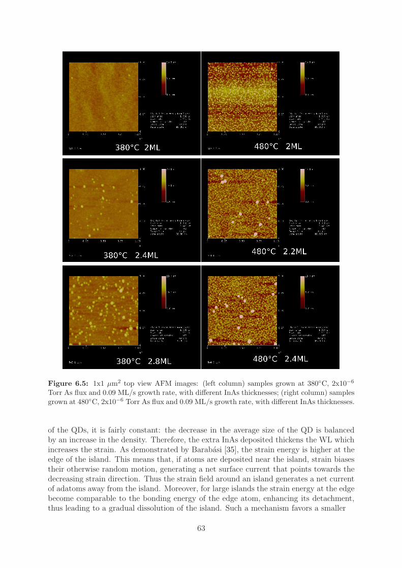
Figure 6.5: 1x1 µm2 top view AFM images: (left column) samples grown at 380◦C, 2x10⁻⁶
Torr As flux and 0.09 ML/s growth rate, with different InAs thicknesses; (right column) samplesgrown at 480◦C, 2x10⁻⁶ Torr As flux and 0.09 ML/s growth rate, with different InAs thicknesses.
of the QDs, it is fairly constant: the decrease in the average size of the QD is balancedby an increase in the density. Therefore, the extra InAs deposited thickens the WL whichincreases the strain. As demonstrated by Barabasi [35], the strain energy is higher at theedge of the island. This means that, if atoms are deposited near the island, strain biasestheir otherwise random motion, generating a net surface current that points towards thedecreasing strain direction. Thus the strain field around an island generates a net currentof adatoms away from the island. Moreover, for large islands the strain energy at the edgebecome comparable to the bonding energy of the edge atom, enhancing its detachment,thus leading to a gradual dissolution of the island. Such a mechanism favors a smaller
63

2 2.1 2.2 2.3 2.41.4
1.5
1.6
1.7
1.8
InAs thickness [ML]
Den
sity
[1011
cm−
2 ]
2 2.1 2.2 2.3 2.422
23
24
25
InAs thickness [ML]
Ave
rage
Dia
met
er [n
m]
2 2.1 2.2 2.3 2.41.6
1.8
2
2.2
2.4
2.6
InAs thickness [ML]
Ave
rage
Hei
ght [
nm]
Figure 6.6: Density, mean diameter and mean height of QDs growth with different InAsthicknesses.
2 2.1 2.2 2.3 2.40.8
1
1.2
1.4
1.6
Total InAs deposited [ML]
Thi
ckne
ss [M
L]
Volume of QDs in MLeq Estimated WL thickness
Figure 6.7: InAs amount absorbed by the QDs and thickness of the WL, depending on thetotal amount of InAs deposited.
average island size.A further increase in deposition amount (2.4 ML) shows bigger QDs size and a reduceddensity. The total volume of InAs absorbed by the QDs, however, does not come fromjust the extra 0.2 ML deposited, as shown in Fig. 6.7, but also from the WL. In this casethe dots erode the WL absorbing InAs from it.To summarize, increasing InAs deposition from 2 ML to 2.2 ML leads to the self-limitingsize effect. The strain reaches a threshold that triggers the detachment of the edge atomsof the QDs, reducing the average size of the QDs. Moreover, the net current flow thatpushes the detached adatoms away from the already formed QDs, induces the formationof new coherent islands, increasing therefore the density number. A further increase ofInAs deposited leads to a strain too high that breaks the previous balance. The strain isrelaxed forming big clusters and increasing the average size of the QDs at the expense ofthe WL that becomes thinner.
64
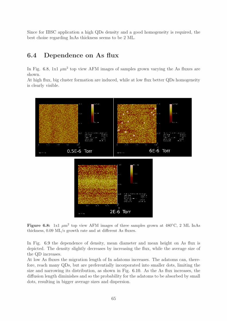
Since for IBSC application a high QDs density and a good homogeneity is required, thebest choise regarding InAs thickness seems to be 2 ML.
6.4 Dependence on As flux
In Fig. 6.8, 1x1 µm2 top view AFM images of samples grown varying the As fluxes areshown.At high flux, big cluster formation are induced, while at low flux better QDs homogeneityis clearly visible.
Figure 6.8: 1x1 µm2 top view AFM images of three samples grown at 480◦C, 2 ML InAsthickness, 0.09 ML/s growth rate and at different As fluxes.
In Fig. 6.9 the dependence of density, mean diameter and mean height on As flux isdepicted. The density slightly decreases by increasing the flux, while the average size ofthe QD increases.At low As fluxes the migration length of In adatoms increases. The adatoms can, there-fore, reach many QDs, but are preferentially incorporated into smaller dots, limiting thesize and narrowing its distribution, as shown in Fig. 6.10. As the As flux increases, thediffusion length diminishes and so the probability for the adatoms to be absorbed by smalldots, resulting in bigger average sizes and dispersion.
65
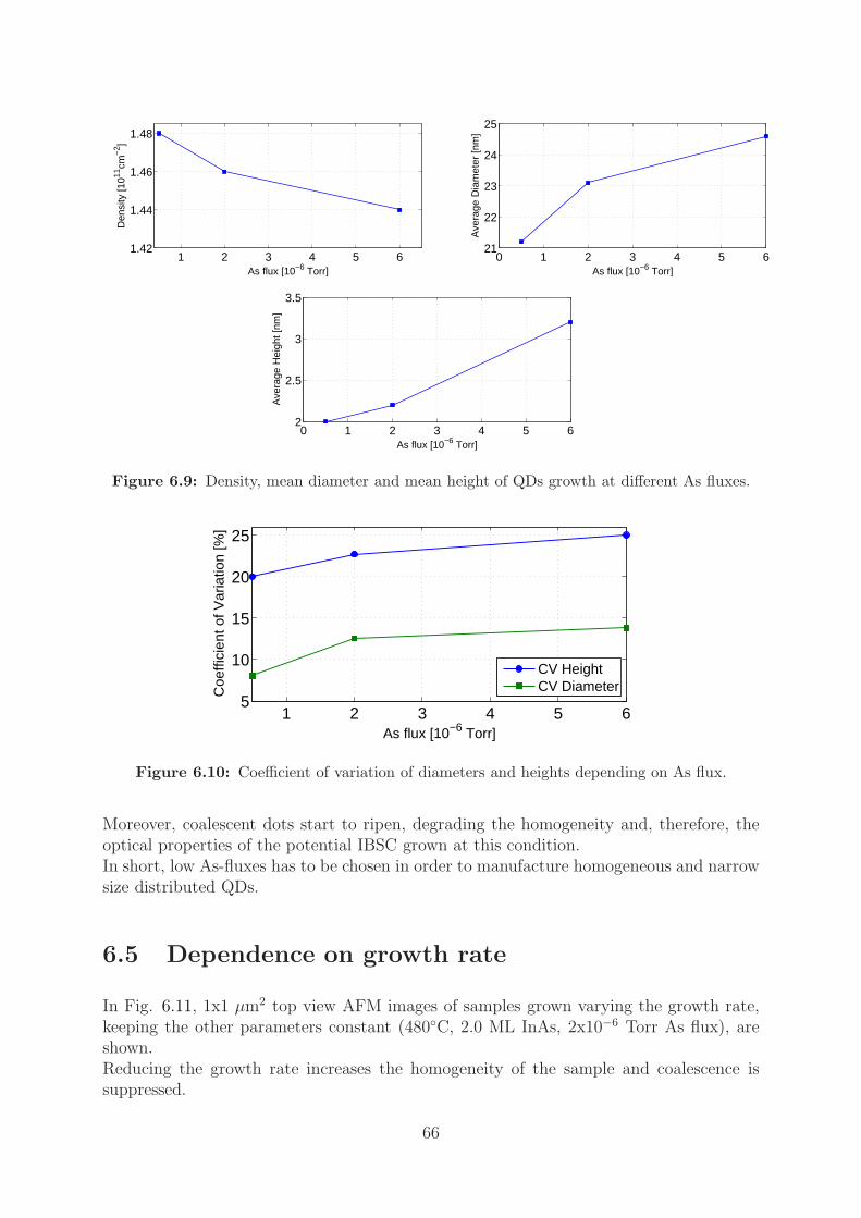
1 2 3 4 5 61.42
1.44
1.46
1.48
As flux [10−6 Torr]
Den
sity
[1011
cm−
2 ]
0 1 2 3 4 5 621
22
23
24
25
As flux [10−6 Torr]
Ave
rage
Dia
met
er [n
m]
0 1 2 3 4 5 62
2.5
3
3.5
As flux [10−6 Torr]
Ave
rage
Hei
ght [
nm]
Figure 6.9: Density, mean diameter and mean height of QDs growth at different As fluxes.
1 2 3 4 5 65
10
15
20
25
As flux [10−6 Torr]
Coe
ffici
ent o
f Var
iatio
n [%
]
CV HeightCV Diameter
Figure 6.10: Coefficient of variation of diameters and heights depending on As flux.
Moreover, coalescent dots start to ripen, degrading the homogeneity and, therefore, theoptical properties of the potential IBSC grown at this condition.In short, low As-fluxes has to be chosen in order to manufacture homogeneous and narrowsize distributed QDs.
6.5 Dependence on growth rate
In Fig. 6.11, 1x1 µm2 top view AFM images of samples grown varying the growth rate,keeping the other parameters constant (480◦C, 2.0 ML InAs, 2x10⁻⁶ Torr As flux), areshown.Reducing the growth rate increases the homogeneity of the sample and coalescence issuppressed.
66

Figure 6.11: 1x1 µm2 top view AFM images of three samples grown at 480◦C, 2 ML InAsthickness, 2x10⁻⁶ Torr As flux and at different growth rates.
In Fig. 6.12, densities, average diameters and heights are illustrated.At high growth rate the density increases in accordance with other reports ([32], [36]).Moreover, similarly to Chia et al.[37], the density seems to reach a saturation point around1.85-1.9x1011 cm−2. The saturation of dot density could be understood by the competi-tion between nucleation rate and nucleation probability. With an increase in growth rate,the nucleation rate increases, leading to a high dot density. Meanwhile, the higher dotdensity may inhibit further nucleation of new dots since the available sites (probability)for nucletion is reduced. At a relatively lower growth rate, the first process dominates,while at a relatively higher growth rate, the first and the second processes might reach adynamic equilibrium, resulting in dot density saturation.Their researches have also underlined a correspondig decrease in the dot size and a nar-rowing of the dot lateral size distribution.We, instead, report a slightly different behavior. The height has an overall reduction asexpected, while the diameter, surprisingly, after a decrease from 0.09 ML/s to 0.5 ML/s,increases again at 1 ML/s. Moreover, as depicted in Fig. 6.13, the CV of the diameter isfairly constant in the range examined, while the CV of height increases. The unexpectedtrend at 1 ML/s can be understood analysing the In:As flux ratio, as it will be discussedin section 6.6. However, as already said, at high rate, big clusters are formed that makesthe samples not good candidate for IBSCs. Therefore, low growth rate has to be chosenfor this purpose.
67

0 0.2 0.4 0.6 0.8 11.4
1.5
1.6
1.7
1.8
1.9
2
In growth rate [ML/s]
Den
sity
[1011
cm
−2 ]
0 0.2 0.4 0.6 0.8 121
21.5
22
22.5
23
23.5
In growth rate [ML/s]
Ave
rage
Dia
met
er [n
m]
0 0.2 0.4 0.6 0.8 11
1.5
2
2.5
In growth rate [ML/s]
Ave
rage
Hei
ght [
nm]
Figure 6.12: Density, average diameter and average height of QDs grown at different growthrates.
0.2 0.4 0.6 0.8 110
15
20
25
30
35
In growth rate [ML/s]
Coe
ffici
ent o
f Var
iatio
n [%
]
CV HeightCV Diameter
Figure 6.13: Coefficient of variation of diameters and heights depending on growth rate.
6.6 Dependence on In:As flux ratio
In this section, the last analysis performed is discussed.In Fig. 6.14 1x1 µm2 top view AFM images of samples grown at different III/V flux ratiosare illustrated (480◦C, 2.0 ML)
68

Figure 6.14: 1x1 µm2 top view AFM images of samples grown at different III/V flux ratio.
At very high flux ratio as well as at low flux ratio, the QDs homogeneity seems compro-mised because of big clusters formation while at ratios ranging from 1/30 to 1/7 goodhomogeneity is produced.Quantitative description of variation of QDs density and sizes depending on In:As ratio isgiven in Fig. 6.15. A turning point in each plot is present at In:As 1/7. Up to this pointthe density increases while the average size decreases. The explanation for this trendrelies on the fact that increasing the III/V ratio increases the In surface migration length,thus increasing the density. Moreover, enhancing the In adatom surface diffusivity in theWL allows it to attain a more thermodinamically equilibrium state with respect to uni-form strain and uniform roughening. A more uniforme strain distribution and roughenedgrowth front will lead to a more uniform island distribution on top of the WL, therefore
69

10−2
10−1
100
1.2
1.4
1.6
1.8
2
In:As flux ratio
Den
sity
[1011
cm−
2 ]
10−2
10−1
100
21
22
23
24
25
In:As flux ratio
Ave
rage
Dia
met
er [n
m]
10−2
10−1
100
1
1.5
2
2.5
3
In:As flux ratio
Ave
rage
Hei
ght [
nm]
Figure 6.15: Density, mean diameter and mean height of QDs growth at different III/V ratios.
narrowing the distribution as shown in Fig. 6.16.
10−2
10−1
100
0
10
20
30
40
In:As flux ratio
Coe
ffici
ent o
f Var
iatio
n [%
]
CV HeightCV Diameter
Figure 6.16: Coefficient of variation of diameters and heights depending on III/V ratio.
After the turning point at ∼ 1/7, the density starts to decrease and the average sizeincreases again, slighlty broadening the distribution. For that sample the ratio was equalto 3, so the In flux was three times higher than the As flux. This is the only sample ofthe entire serie grown at flux ratio where the In flux was higher than the As flux. Atthis unusual condition, the kinetic process of QDs formation is different from the normalcondition In:As <1. In this regime, after a small InAs coverage, In forms a metallic layeron the GaAs buffer surface. After a certain critical thickness, in order to minimize the
70

strain, the Inlayer starts to ripen in drops, forming QDs with a very high In content. It istherefore probably misleading to compare ratios <1 with ratios >1. It may also be for thesame qualitative reason that the dependence on the InAs growth analysed in the previoussection was a little bit different from the reported ones. The sample grown at 1 ML/s isthe one with In:As flux ratio 3:1.To summarize, comparing homogeneity and quantitative data, the best choise of III/Vflux ratio for IBSC application lies in the range 1/10 - 1/5, while due to speculations onthe process involved in QDs formation at III/V ratio >1, the sample at III/V = 3 shouldnot be directly compared with the other ones. In this case the growth rate dependencediscussed in section 6.5 confirms the results of several other works ([32], [36] and [37]).
71


Chapter 7
Conclusion
The influence of the conditions during growth of InAs/GaAs quantum-dot structures onGaAs(001) by molecular-beam epitaxy has been investigated systematically with respectto achieving high quantum dot densities, homogeneity and narrow sizes distribution. Thegrowth temperature, InAs deposit, As flux, growth rate and III/V flux ratio were varied.Atomic force microscopy and a modular program for SPM data analysis have been usedto study the morphological properties of the QDs. First, the image processing has beenstudied in order to verify the effect that every operation has on the image. Afterward,with the routine defined, all the samples have been analysed.
Removing polynomial background from the AFM images reduces the heights and thediameters of the QDs if they are not excluded from this operation while, if they areexcluded it does not affect the original data, regardless which degree polynom used. De-convoluting the image and the AFM reduces the mean height and narrow its normaldistribution, while the mean diameter increases and the distribution broadens. Moreover,low pass filtering the image does not change the FWHMs of the diameters and heightsdistribution while reduces the mean height and diameter.The estimated errors for density, mean diameter and mean height has been set to 3.5%,7.5% and 4.5% respectively.
QDs are not devepoled at temperature ranging from 360◦C to 400◦C. The lowest tem-perature at which 2D-3D transition is visible is 420◦C for the growth conditions used inthis work. Increasing the growth temperature to 480◦C leads to a decrease in the densityand an increase in the average QD size, although the distributions narrow. The resultis in agreement with the model of self-limited growth in the S-K model, which predictincreasing island volume increasing the temperature and, thus, the coefficient of In surfacediffusion.Increasing InAs deposition from 2 ML to 2.2 ML leads to the self-limiting size effect.The strain reaches a threshold that triggers the detachment of the edge atoms of theQDs, reducing the average size of the QDs. Moreover, the net current flow that pushesthe detached adatoms away from the already formed QDs, induces the formation of newcoherent islands, increasing therefore the density number. A further increase of InAs de-posited leads to a strain too high that breaks the previous balance. The strain is relaxedforming big clusters and increasing the average size of the QDs at the expense of the WL
73

that becomes thinner.At low As fluxes the migration length of In adatoms increases. The adatoms can, there-fore, reach many QDs, but are preferentially incorporated into smaller dots, limiting thesize and narrowing its distribution. As the As flux increases, the diffusion length dimin-ishes and so the probability for the adatoms to be absorbed by small dots, resulting inbigger average sizes and dispersion. Moreover, coalescent dots start to ripen, degradingthe homogeneity.At very high flux ratio as well as at low flux ratio, the QDs homogeneity seems com-promised because of big clusters formation. The sample at ratio equal to 3 is excludedfrom the serie because different processes than the S-K growth mode are involved in QDsformation if the In flux is higher than the As flux. Increasing the In:As flux ratio enhancesthe density and reduces the average QDs size, narrowing also the distributions. It relieson the fact that increasing the III/V ratio increases the In surface migration length and itallows the WL to attain a more uniform strain distribution that leads to a more uniformisland distribution.Finally, increasing the growth rate the density increases while the average size decreases.The coefficient of variation of the diameters is not affected while for the heights it in-creases.Therefore the optimized growth conditions are: 480◦C, 2 ML InAs deposit, 0.5x10⁻⁶ TorrAs flux, 0.09 ML/s growth rate, leading to a III/V ratio of 1/9.
74


Appendices
77


Appendix A
AFM Images
79

A.1 541-1
80

81

82

A.2 541-2
83

84
85

A.3 541-3
86

87

88

A.4 541-4
89

90

91

A.5 542-1
92

93

94

A.6 542-3
95

96
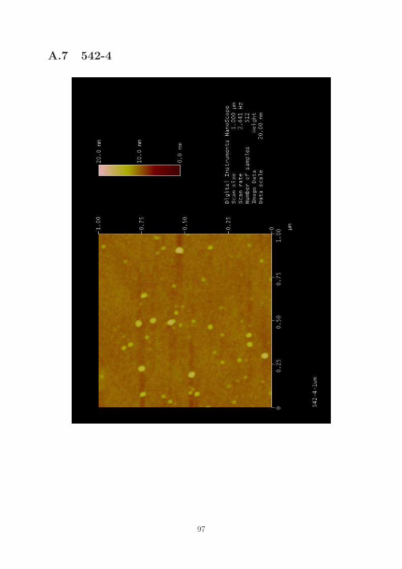
A.7 542-4
97

98

99

A.8 543-1
100

101

102

A.9 543-2
103

104
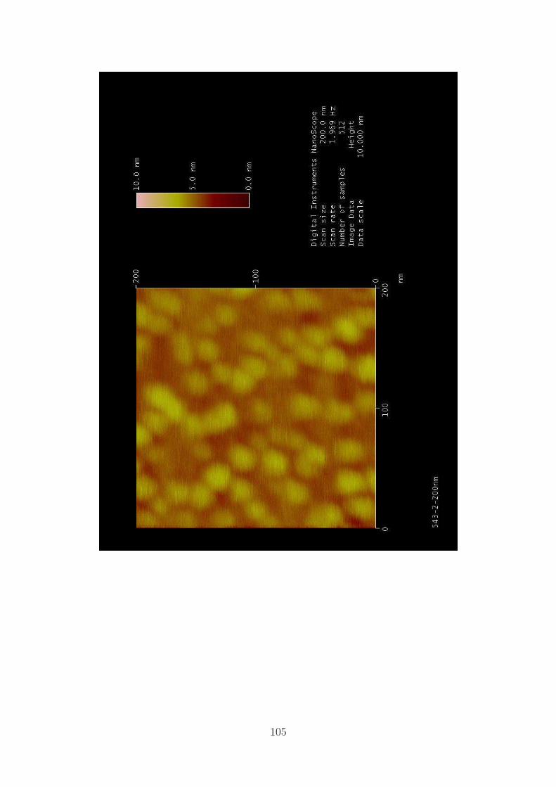
105

A.10 543-3
106

107

108

A.11 544-1
109

110
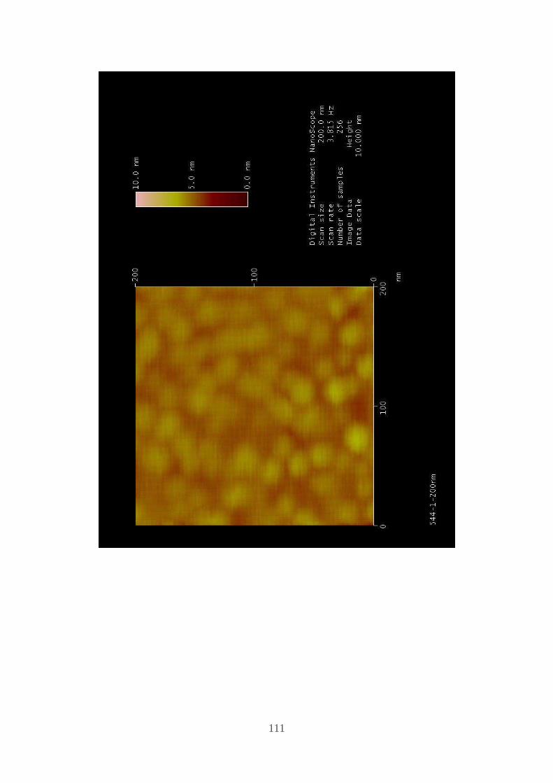
111

A.12 544-2
112

113

114

A.13 547-1
115

116

117

A.14 547-2
118

119

120


Appendix B
Matlab Codes
B.1 MATLAB code for diameter analysis
% LOAD RAW DATA
A=load(’raw_data_imageA.txt’);
B=load(’raw_data_imageB.txt’);
C=load(’raw_data_imageC.txt’);
x=5:0.5:60;
% CREATE THE HISTOGRAM OF DIAMETERS OF IMAGE A
% AND CALCULATE THE FITTING NORMAL DISTRIBUTION
diameter_nmA=2*10^(9)*A(:,3);
mu_diameter_A=mean(diameter_nmA);
sigma_diameter_A=std(diameter_nmA);
[bincounts_diameter_A,binpositions_diameter_A] = hist(diameter_nmA,x);
binwidth_diameter_A = binpositions_diameter_A(2) - binpositions_diameter_A(1);
histarea_diameter_A = binwidth_diameter_A*sum(bincounts_diameter_A);
x_diameter_A = binpositions_diameter_A(1):0.001:binpositions_diameter_A(end);
y_diameter_A = normpdf(x_diameter_A,mu_diameter_A,sigma_diameter_A);
% CREATE THE HISTOGRAM OF DIAMETERS OF IMAGE B
% AND CALCULATE THE FITTING NORMAL DISTRIBUTION
diameter_nmB=2*10^(9)*B(:,3);
mu_diameter_B=mean(diameter_nmB);
sigma_diameter_B=std(diameter_nmB);
[bincounts_diameter_B,binpositions_diameter_B] = hist(diameter_nmB,x);
123

binwidth_diameter_B = binpositions_diameter_B(2) - binpositions_diameter_B(1);
histarea_diameter_B = binwidth_diameter_B*sum(bincounts_diameter_B);
x_diameter_B = binpositions_diameter_B(1):0.001:binpositions_diameter_B(end);
y_diameter_B = normpdf(x_diameter_B,mu_diameter_B,sigma_diameter_B);
% PLOT THE HISTOGRAMS OF DIAMETERS OF IMAGE A AND B
subplot(2,2,1)
hist(diameter_nmA,x);
xlabel(’Diameter [nm]’);
ylabel(’Counts [arb.un.]’);
subplot(2,2,3)
hist(diameter_nmB,x);
xlabel(’Diameter [nm]’);
ylabel(’Counts [arb.un.]’);
% PLOT THE NORMAL DISTRIBUTION OF DIAMETERS OF IMAGE A AND B
subplot(2,2,[2 4])
plot(x_diameter_A,histarea_diameter_A*y_diameter_A,x_diameter_B,histarea_diameter_B*y_diameter_B);
xlabel(’Diameter [nm]’);
ylabel(’Counts [arb.un.]’);
title(’Normal Distribution Fitting’);
124

B.2 MATLAB code for height analysis
% LOAD RAW DATA
A=load(’raw_data_imageA.txt’);
B=load(’raw_data_imageB.txt’);
x=0:0.3:5;
% CREATE THE HISTOGRAM OF HEIGHTS OF IMAGE A
% AND CALCULATE THE FITTING NORMAL DISTRIBUTION
height_mA=A(:,2)-A(:,1);
height_nmA= 10^(9)*height_mA;
mu_height_A=mean(height_nmA);
sigma_height_A=std(height_nmA);
[bincounts_height_A,binpositions_height_A] = hist(height_nmA,x);
binwidth_height_A = binpositions_height_A(2) - binpositions_height_A(1);
histarea_height_A = binwidth_height_A*sum(bincounts_height_A);
x_height_A = binpositions_height_A(1):0.001:binpositions_height_A(end);
y_height_A = normpdf(x_height_A,mu_height_A,sigma_height_A);
% CREATE THE HISTOGRAM OF HEIGHTS OF IMAGE B
% AND CALCULATE THE FITTING NORMAL DISTRIBUTION
height_mB=B(:,2)-B(:,1);
height_nmB= 10^(9)*height_mB;
mu_height_B=mean(height_nmB);
sigma_height_B=std(height_nmB);
[bincounts_height_B,binpositions_height_B] = hist(height_nmB,x);
binwidth_height_B = binpositions_height_B(2) - binpositions_height_B(1);
histarea_height_B = binwidth_height_B*sum(bincounts_height_B);
x_height_B = binpositions_height_B(1):0.001:binpositions_height_B(end);
y_height_B = normpdf(x_height_B,mu_height_B,sigma_height_B);
% PLOT THE HISTOGRAMS OF HEIGHTS OF IMAGE A AND B
subplot(2,2,1)
hist(height_nmA,x);
xlabel(’Height [nm]’);
ylabel(’Counts [arb.un.]’);
125

subplot(2,2,3)
hist(height_nmB,x);
xlabel(’Height [nm]’);
ylabel(’Counts [arb.un.]’);
% PLOT THE NORMAL DISTRIBUTION OF HEIGHTS OF IMAGE A AND B
subplot(2,2,[2 4])
plot(x_height_A,histarea_height_A*y_height_A,x_height_B,histarea_height_B*y_height_B);
xlabel(’Height [nm]’);
ylabel(’Counts [arb.un.]’);
title(’Normal Distribution Fitting’);
126

B.3 MATLAB code for calculating QDs total volume
in MLeq
% LOAD RAW DATA
A=load(’raw_data_imageA.txt’);
B=load(’raw_data_imageB.txt’);
% SUM OF QDs SINGLE VOLUMES AND CONVERSION IN MLeq FOR IMAGE A
A_sum_volume=sum(A);
ML_eq_A = (10^(27)*A_sum_volume(1,5))/(500^(2)*0.3);
% SUM OF QDs SINGLE VOLUMES AND CONVERSION IN MLeq FOR IMAGE B
B_sum_volume=sum(B);
ML_eq_B = (10^(27)*B_sum_volume(1,5))/(500^(2)*0.3);
127

Bibliography
[1] A. Martı and A. Luque, Next Generation Photovoltaics, high efficiency through full
spectrum utilization. Institute of Physics, Bristol and Philadelphia, 2004.
[2] M. A. Green, “Photovoltaics: technology overview,” Energy Policy, vol. 28, no. 14,pp. 989–998, 2000.
[3] ——, “Third generation photovoltaics: solar cells for 2020 and beyond,” Physica E,vol. 14, pp. 65–70, 2002.
[4] D. M. Chapin, C. S. Fuller, and G. L. Pearson, “A new silicon p-n junction photocellfor converting solar radiation into electrical power,” J. Appl. Phys., vol. 25, pp. 676–677, 1954.
[5] D. M. Bagnall and M. Boreland, “Photovoltaic technologies,” Energy Policy, vol. 36,pp. 4390–4396, 2008.
[6] M. A. Green, “Recent developments in photovoltaics,” Solar Energy, vol. 76, pp. 3–8,2004.
[7] R. W. Miles, K. M. Hynes, and I. Forbes, “Photovoltaic solar cells: An overviewof state-of-the-art cell development and environmental issues,” Progress in Crystal
Growth and Characterization of Materials, vol. 51, pp. 1–42, 2005.
[8] [Online]. Available: www.nrel.gov
[9] L. L. Kazmerski, “Solar photovoltaics r&d at the tipping point: A 2005 technologyoverview,” Journal of Electron Spectroscopy and Related Phenomena, vol. 150, pp.105–135, 2006.
[10] G. Conibeer, “Third-generation photovoltaics,” Materials Today, vol. 10, pp. 42–50,2007.
[11] M. A. Green, “Third generation photovoltaics: Ultra-high conversion efficiency at lowcost,” Prog.Photovolt: Res. Appl., vol. 9, pp. 123–135, 2001.
[12] W. Shockley and H. J. Queisser, “Detailed balanced limit of efficiency of p-n junctionsolar cell,” J. Appl. Phys., vol. 32, pp. 510–519, 1961.
[13] A. Martı and G. L. Araujo, “Limiting efficiencies for photovoltaic energy conversionin multigap systems,” Solar Energy Materials and Solar Cells, vol. 43, pp. 203–222,1996.
129

[14] P. Wurfel, “Solar energy conversion with hot electrons from impact ionisation,”Solar
Energy Materials and Solar Cells, vol. 46, pp. 43–52, 1997.
[15] A. Luque and A. Martı, “Increasing the efficiency of ideal solar cells by photon inducedtransition at intermediate levels,” Phys. Rev. Lett., vol. 78, pp. 5014–5017, 1997.
[16] A. Martı, N. Lopez, E. Antolın, E. Canovas, C. Stanley, C. Farmer, L. Cuadra, andA. Luque, “Novel semiconductor solar cell structure: The quantum dot intermediateband solar cell,” Thin Solid Films, vol. 511-512, pp. 638–644, 2006.
[17] A. Martı, C. Stanley, and A. Luque, Nanostructured Material for Solar Energy Con-
version. Elsevier, 2006, ch. 17.
[18] L. Cuadra, A. Luque, and A. Martı, “Present status of intermediate band solar cellresearch,” Thin Solid Films, vol. 451-452, pp. 593–599, 2004.
[19] P. Harrison, Quantum Wells, Wires and Dots: Theoretical and Computational
Physics. Wiley & Sons, 1999.
[20] S. Tomic, N. Harrison, and T. Jones, “Electronic structure of QD arrays: applicationto intermediate-band solar cells,” Opt. Quant. Electron., vol. 40, pp. 313–318, 2008.
[21] A. Martı, L. Cuadra, and A. Luque, “Design constraints of the quantum dot inter-mediate band solar cell,” Physica E, vol. 14, pp. 150–157, 2002.
[22] M. Henini, Handbook of Self Assembled Semiconductor Nanostructures for Novel De-
vices in Photonics and Electronics. Elsevier, 2008, ch. 3.
[23] E. Placidi, F.Arciprete, M. Fanfoni, F. Patella, E. Orsini, and A. Balzarotti,“InAs/GaAs(001) epitaxy: kinetic effects in the two-dimensional to three-dimensionaltransition,” J. Phys.: Condens. Matter, vol. 19, pp. 1–21, 2007.
[24] A. Cullis, D. Norris, T. Walther, M. Migliorato, and M. Hopkinson, “Stranski-krastanow transition and epitaxial island growth,” Phys. Rev. B, vol. 66, 2002.
[25] P. Dowben and A. Miller, Surface Segregation Phenomena. CRC Press, 1990.
[26] G. Costantini, A. Rastelli, C. Manzano, P.Acosta-Diaz, R. Songmuang, G. Kat-saros, O. Schmidt, and K. Kern, “Interplay between thermodynamics and kinetics ofInAs/GaAs(001) quantum dots,” Phys. Rev. Lett., vol. 96, 2006.
[27] P. Joyce, T. Krzyzewski, G. Bell, and T. Jones, “Surface morphology evolution duringthe overgrowth of large InAs-GaAs quantum dots,” Appl. Phys. Lett., vol. 79, 2001.
[28] F. Ferdos, S. Wang, Y. Wei, A. Larsson, M. Sadeghi, and Q. Zhao, “Influence ofa thin GaAs cap layer on structural and optical properties of InAs quantum dots,”Appl. Phys. Lett., vol. 81, 2002.
[29] H. Eisele, A. Lenz, R. Heitz, R. Timm, M. Dahne, Y. Temko, T. Suzuki, and K. Ja-cobi, “Change of InAs/GaAs quantum dot shape and composition during capping,”J. Appl. Phys., vol. 104, 2008.
[30] [Online]. Available: http://gwyddion.net/
[31] [Online]. Available: http://gwyddion.net/documentation/
130

[32] T. Passow, S. Li, P. Feinaugle, T. Vallaitis, J. Leuthold, D. Litvinov, D. Gerthsen,and M. Hetterich, “Systematic investigation into the influence of growth conditionson InAs/GaAs quantum dot properties,” J. Appl. Phys., vol. 102, 2007.
[33] D. Zhou, G. Sharma, S. F. Thomassen, T. W. Reenaas, and B. O. Fimland, “Opti-mization towards high density quantum dots for intermediate band solar cells grownby molecular beam epitaxy,” Appl. Phys. Lett., vol. 96, 2010.
[34] N. Cherkashin, M. Maksimov, A. Makarov, V. Shchukin, V. Ustinov, N. Lukovskaya,Y. Musikhin, G. Cirlin, N. Bert, Z. Alferov, N. Ledentsov, and D. Bimberg, “Controlover the Parameters of InAs/GaAs Quantum Dot Arrays in the Stranski-KrastanowGrowth Mode,” Semiconductors, vol. 37, pp. 861–865, 2003.
[35] A. L. Barabasi, “Self-assembled island formation in heteroepitaxial growth,” Appl.
Phys. Lett., vol. 70, pp. 2565–2567, 1997.
[36] P. Joyce, T. Krzyzewski, G. Bell, T. Jones, S. Malik, D. Childs, and R. Murray,“Effect of growth rate on the size, composition, and optical properties of InAs/GaAsquantum dots grown by molecular-beam epitaxy,” Phys. Rev. B, vol. 62, pp. 10 891–10 895, 2000.
[37] C. Chia, Y. Zhang, S. Wong, A. Yong, S. Chow, S. Chua, and J. Guo, “Saturateddot density of InAs/GaAs self-assembled quantum dots grown at high growth rate,”Appl. Phys. Lett., vol. 90, 2007.
131


![Integrazione con metodo Monte Carlo - math.unipd.itantonelm/teaching/R_1011/montecarlo_slides.pdf · var[g(u)] L’errore pu`o quindi scriversi come deviazione standard ... rispetto](https://img.pdfslide.net/doc/110x75/5bc306db09d3f2d7198b7176/integrazione-con-metodo-monte-carlo-mathunipdit-antonelmteachingr1011montecarlo.jpg)