Embed Size (px)
Citation preview

Subscriber access provided by JAWAHARLAL NEHRU CENTER
The Journal of Physical Chemistry C is published by the American ChemicalSociety. 1155 Sixteenth Street N.W., Washington, DC 20036
Article
Conducting Nanocrystal Patterns Using a Silver OrganicComplex Blended with Polystyrene as e-Beam Resist
T. Bhuvana, C. Subramaniam, T. Pradeep, and G. U. KulkarniJ. Phys. Chem. C, 2009, 113 (17), 7038-7043• DOI: 10.1021/jp811062m • Publication Date (Web): 02 April 2009
Downloaded from http://pubs.acs.org on April 23, 2009
More About This Article
Additional resources and features associated with this article are available within the HTML version:
• Supporting Information• Access to high resolution figures• Links to articles and content related to this article• Copyright permission to reproduce figures and/or text from this article
Conducting Nanocrystal Patterns Using a Silver Organic Complex Blended withPolystyrene as e-Beam Resist
T. Bhuvana,† C. Subramaniam,‡ T. Pradeep,‡ and G. U. Kulkarni*,†
Chemistry and Physics of Materials Unit and DST Unit on Nanoscience, Jawaharlal Nehru Centre forAdVanced Scientific Research, Jakkur P O, Bangalore 560 064, India, DST Unit on Nanoscience,Department of Chemistry and Sophisticated Analytical Instrument Facility, Indian Institute of TechnologyMadras, Chennai 600036, India,
ReceiVed: December 15, 2008; ReVised Manuscript ReceiVed: February 23, 2009
With the intention of producing a metal composite consisting of Ag nanoparticles embedded in patternedpolystyrene, silver triphenylphosphine nitrate, Ag(PPh3)3NO3, was chosen as a source of Ag metal as it issoluble in toluene to form a blend with polystyrene, a well-known negative tone e-beam resist. At a constante-beam dosage of 150 µC cm-2, the patterns were produced at 5, 10, and 30 keV beam energies while varyingthe dwell time at a location (pixel) and the number of passes. The presence of Ag in the patterned regionswas confirmed by the EDS analysis. TEM showed the formation of small Ag nanoparticles in the embeddedmatrix of the polymer. The reduction of Ag precursor following exposure to the e beam was monitored byXPS. UV-vis absorption studies showed a broad peak at 464 nm, typical of surface plasmon absorption byAg nanoparticles. Confocal fluorescence studies showed the embedded Ag nanoparticles in the carbon matrixto have fluorescence property as well. C-AFM measurements have shown that the patterned blend is wellconducting due to the interacting Ag nanoparticles, the resistance being two orders less compared to that ofpolystyrene itself. The higher the beam energy, the lower was the dwell time required to attain a conductingpattern.
Introduction
Design and synthesis of patternable nanomaterials is importantto device fabrication. In this context, UV or e-beam lithographybased synthesis of patterned nanomaterials for active elementsis a versatile method. Metal precursors containing polymerblends are good starting materials for this purpose, as the formerproduces active species under the lithography beam while thelatter not only works like a resist but also provides the desiredmatrix. One such example is the spin-coatable e-beam sensitiveresist consisting of metal nitrate salts and polyvinyl alcohol(PVA) based blend, which gave rise to La0.7Sr0.3MnO3 patterns.1
With regard to metal systems, Abargues et al.2 reported a high-resolution negative-tone nanocomposite resist based on PVAwhere Ag nanoparticles and nanopatterns were simultaneouslygenerated by the e-beam lithography. Such metal-polymerpatterns may find applications in nanocircuitry and plasmonicdevices. We have been interested in developing precursors fordirect write lithography3 and in this article, we explore thereduction of an Ag salt in polystyrene matrix upon exposure tothe e-beam, the polymer itself known to be a negative toneresist.4
There are many reports on polymer blends embedded withAg nanoparticles, though not directly related to lithography.Bogle et al.5 reported the synthesis of Ag nanoparticles byirradiating a solution of AgNO3 and PVA, with 6 MeV electronswhereas Mahapatra et al.6 used a mixture of PVA with Au andAg metal precursors and obtained respective metal nanoparticlesby exposure to a broad e-beam of 5-15 keV. Eilers et al.7
obtained Teflon-Ag nanocomposite by thermal evaporation ofTeflon and Ag foil on sapphire substrate and found thebroadening of optical absorption indicating the formation of theblend. Porel et al.8 have synthesized Ag and Au nanoparticlesin polyvinyl alcohol (PVA) matrix by heating a mixture of themetal salt and PVA and investigated the optical limitingcapability of these nanoparticle-embedded polymer blends.There are other studies where the blend contained well-knownresists such as poly(methylmethacrylate) (PMMA), although nopatterning was attempted. Deshmukh and Composto9 showedthat the thermal decomposition of Ag precursor with PMMAat 185 °C leads to the formation of Ag nanoparticles and theirenrichment at the surface. Basak et al.10,11 have studied thephotoluminescence and electrical conductivity of thin films ofPMMA dispersed with Ag nanoparticles. The authors showedthat the electrical conduction was caused by the conducting pathsestablished through the proximal interaction between neighbor-ing nanoparticles.
In this article, we report our investigations on a blend ofAg(PPh3)3NO3-polystyrene used as a e-beam resist for pat-terning. Our intention was to exploit the e-resist behavior ofpolystyrene and doping it with metallic Ag species to improveits electrical conduction behavior and thus produce conductingpatterns. We have carried out detailed characterization of thewritten patterns using X-ray photoelectron spectroscopy (XPS),transmission electron (TEM), and scanning transmission (STEM)microscopy as well as confocal fluorescence and Ramanspectroscopy. Further, we have examined the electrical conduc-tion behavior of the written patterns using conducting-AFM (C-AFM). Our results have shown that moderate e-beam exposuresconvert the resist blend into patterns filled with Ag nanocrystalsin carbon matrix with good electrical conduction property.
* To whom correspondence should be addressed. E-mail: [email protected]. Fax: +91-80-22082766.
† Jawaharlal Nehru Centre for Advanced Scientific Research.‡ Indian Institute of Technology Madras.
J. Phys. Chem. C 2009, 113, 7038–70437038
10.1021/jp811062m CCC: $40.75 2009 American Chemical SocietyPublished on Web 04/02/2009
Experimental Section
The Ag precursor, namely its triphenylphosphine nitrate(Ag(PPh3)3NO3) was prepared following a literature procedure.12
In order to perform e-beam lithography, the resist was preparedby blending a saturated solution of the Ag precursor in toluenewith commercially available polystyrene (Mw ) 260 000) suchthat the resulting solution had 1 wt % of polystyrene. This blendwas spin-coated at 3000 rpm on clean Si, SiO2/Si, and ITOsubstrates. Electron beam lithography (EBL), was performedon the blend film coated on a Si substrate using an e-beam writeravailable with Nova NanoSEM 600 equipment (FEI Co., TheNetherlands). An array of 8 × 8 µm2 square regions was exposedto e-dosage of 150 µC cm-2 at different beam energies 5-30kV. For the negative tone behavior of polystyrene, this dosageis adequate.13 Electron exposure was carried out with constante-dosage while varying internal parameters such as the dwelltime and number of passes. The substrate was then developedin p-xylene and 2-propanol for 90 and 30 s, respectively, as isusually done for polystyrene.14 Further, the patterned substratewas dried under flowing nitrogen. The procedure is shown inthe scheme in Figure 1. For a 60 µL of the blend, the patternthickness achieved was typically 180 nm, as revealed in thestep measurements using an optical profilometer (NT1100,Wyko, Veeco Instruments, USA).
Energy dispersive spectroscopy (EDS) analysis was per-formed at 10 kV (energy window, 10 eV) with a beam currentof 1.1 nA, the dwell time per pixel being 30 µs using an EDAXGenesis (Mahwah, USA), attached to the SEM column. STEM(scanning transmission electron microscopy) was also performedusing the same equipment. UV-visible spectra were recordedusing a Perkin-Elmer Lambda 900 UV/vis/NIR spectropho-tometer. The core-level Ag(3d) spectra were measured using aVG scientific ESCALAB MK-IV spectrophotometer with anX-ray source of Al KR (1486.6 eV). In order to performtransmission electron microscopy (TEM), a holey carbon gridwas drop coated with the blend and patterned. High-resolutionTEM imaging was carried out with a JEOL-3010 equipmentoperating at 300 kV. C-AFM measurements using Au coatedtips15 were performed on patterned ITO substrate employing aDigital Instruments Multimode head attached to a Nanoscope-IV controller (Veeco, USA) and an external multimeter (Kei-thley 236). The Raman and fluorescence spectra were collected
using patterned ITO with 514.5 nm Ar ion laser excitation (spotsize <1 µm). The laser beam power was ∼15 mW. Thebackscattered light was collected using a 100× objective lensand typical signal acquisition time at each pixel of the imagewas 0.1 s.
Results and Discussion
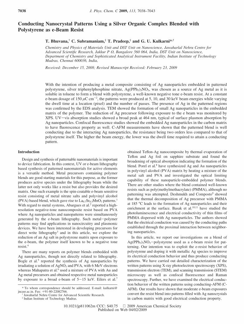
In Figure 1, are shown the patterns drawn using aAg(PPh3)3NO3-polystyrene blend for e-beam lithography. Aspolystyrene is a negative-tone resist, the e-beam exposed regionsget cross-linked and remain after developing while rest of thepolymer gets washed away. Figure 1a shows the SEM imageof a ∼500 nm gap electrode patterned with the blend resist withan e-dose of 150 µC cm-2 with 5 kV. The EDS mapping at AgM and C K lines showed clearly the presence of Ag and C inthe patterned regions (Figure 1, panels b and c). The roughnessassociated with the edges of the pattern was ∼3 nm typical ofpolystyrene itself.16 The atomic ratio of Ag and carbon asdetermined by EDS was 6:94.
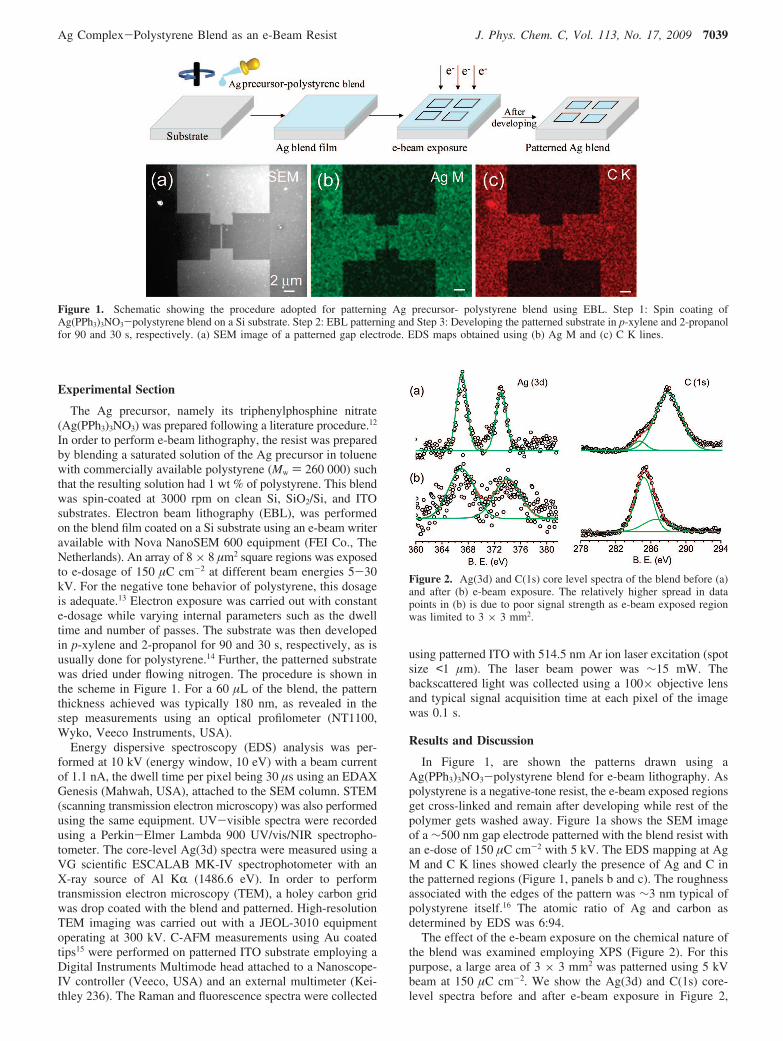
The effect of the e-beam exposure on the chemical nature ofthe blend was examined employing XPS (Figure 2). For thispurpose, a large area of 3 × 3 mm2 was patterned using 5 kVbeam at 150 µC cm-2. We show the Ag(3d) and C(1s) core-level spectra before and after e-beam exposure in Figure 2,
Figure 1. Schematic showing the procedure adopted for patterning Ag precursor- polystyrene blend using EBL. Step 1: Spin coating ofAg(PPh3)3NO3-polystyrene blend on a Si substrate. Step 2: EBL patterning and Step 3: Developing the patterned substrate in p-xylene and 2-propanolfor 90 and 30 s, respectively. (a) SEM image of a patterned gap electrode. EDS maps obtained using (b) Ag M and (c) C K lines.
Figure 2. Ag(3d) and C(1s) core level spectra of the blend before (a)and after (b) e-beam exposure. The relatively higher spread in datapoints in (b) is due to poor signal strength as e-beam exposed regionwas limited to 3 × 3 mm2.
Ag Complex-Polystyrene Blend as an e-Beam Resist J. Phys. Chem. C, Vol. 113, No. 17, 2009 7039
panels a and b, respectively. Prior to e-beam exposure, theAg(3d) spin-orbit doublets are observed at 367.2 and 373.1eV (Figure 2a) and after e-dosage, at 367.0 and 373.9 eV (Figure2b) and the area under the curves being nearly same. Ag(3d)peak became broad and shifted slightly to a lower bindingenergy. Considering Ag(3d) shows only a small shift from Ag+
to Ag0 (∼0.3 eV),17 the above observation is taken to indicatethe reduction of the Ag complex. The C(1s) region, prior toexposure (Figure 2a) was found to contain two features at 284.6and 287.8 eV due to graphitic and sp3 carbon respectively,whereas after e-beam exposure (Figure 2b), the main peakposition shifted to 285.3 and with a lower intensity peak at 286.6eV. The shift to a lower binding energy is taken to indicate theformation of more graphitic carbon in comparison to hydro-carbon before exposure to e-beam.
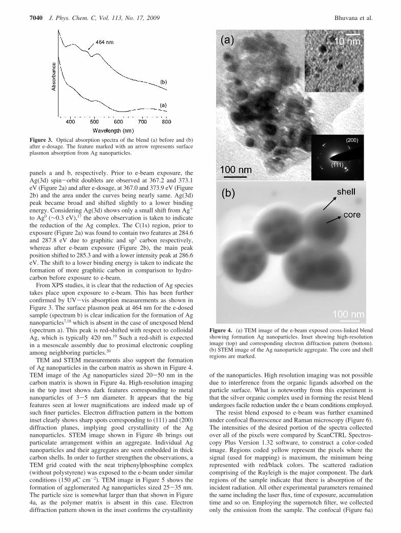
From XPS studies, it is clear that the reduction of Ag speciestakes place upon exposure to e-beam. This has been furtherconfirmed by UV-vis absorption measurements as shown inFigure 3. The surface plasmon peak at 464 nm for the e-dosedsample (spectrum b) is clear indication for the formation of Agnanoparticles7,18 which is absent in the case of unexposed blend(spectrum a). This peak is red-shifted with respect to colloidalAg, which is typically 420 nm.19 Such a red-shift is expectedin a mesoscale assembly due to proximal electronic couplingamong neighboring particles.20
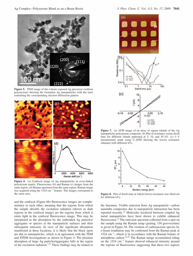
TEM and STEM measurements also support the formationof Ag nanoparticles in the carbon matrix as shown in Figure 4.TEM image of the Ag nanoparticles sized 20-50 nm in thecarbon matrix is shown in Figure 4a. High-resolution imagingin the top inset shows dark features corresponding to metalnanoparticles of 3-5 nm diameter. It appears that the bigfeatures seen at lower magnifications are indeed made up ofsuch finer particles. Electron diffraction pattern in the bottominset clearly shows sharp spots corresponding to (111) and (200)diffraction planes, implying good crystallinity of the Agnanoparticles. STEM image shown in Figure 4b brings outparticulate arrangement within an aggregate. Individual Agnanoparticles and their aggregates are seen embedded in thickcarbon shells. In order to further strengthen the observations, aTEM grid coated with the neat triphenylphosphine complex(without polystyrene) was exposed to the e-beam under similarconditions (150 µC cm-2). TEM image in Figure 5 shows theformation of agglomerated Ag nanoparticles sized 25-35 nm.The particle size is somewhat larger than that shown in Figure4a, as the polymer matrix is absent in this case. Electrondiffraction pattern shown in the inset confirms the crystallinity
of the nanoparticles. High resolution imaging was not possibledue to interference from the organic ligands adsorbed on theparticle surface. What is noteworthy from this experiment isthat the silver organic complex used in forming the resist blendundergoes facile reduction under the e beam conditions employed.
The resist blend exposed to e-beam was further examinedunder confocal fluorescence and Raman microscopy (Figure 6).The intensities of the desired portion of the spectra collectedover all of the pixels were compared by ScanCTRL Spectros-copy Plus Version 1.32 software, to construct a color-codedimage. Regions coded yellow represent the pixels where thesignal (used for mapping) is maximum, the minimum beingrepresented with red/black colors. The scattered radiationcomprising of the Rayleigh is the major component. The darkregions of the sample indicate that there is absorption of theincident radiation. All other experimental parameters remainedthe same including the laser flux, time of exposure, accumulationtime and so on. Employing the supernotch filter, we collectedonly the emission from the sample. The confocal (Figure 6a)
Figure 3. Optical absorption spectra of the blend (a) before and (b)after e-dosage. The feature marked with an arrow represents surfaceplasmon absorption from Ag nanoparticles.
Figure 4. (a) TEM image of the e-beam exposed cross-linked blendshowing formation Ag nanoparticles. Inset showing high-resolutionimage (top) and corresponding electron diffraction pattern (bottom).(b) STEM image of the Ag nanoparticle aggregate. The core and shellregions are marked.
7040 J. Phys. Chem. C, Vol. 113, No. 17, 2009 Bhuvana et al.
and the confocal (Figure 6b) fluorescence images are comple-mentary to each other, meaning that the regions from whichthe sample absorbs the excitation radiation (shown as darkregions in the confocal image) are the regions from which itemits light in the confocal fluorescence image. This may beinterpreted as the absorption by the embedded Ag particles/aggregates or species at the nanoparticle surfaces and theirsubsequent emission. In view of the significant absorptionmanifested at these locations, it is likely that the black spotsare due to nanoparticles, which is in agreement with the TEMand STEM investigations as shown in Figure 4. The plasmonabsorption of large Ag particles/aggregates falls in the regionof the excitation radiation.7,21 These findings may be related to
the literature. Visible emission from Ag nanoparticle-carbonnanotube composites due to nanoparticle interaction has beenreported recently.22 Molecules localized between coupled Agmetal nanoparticles have been shown to exhibit enhancedfluorescence.23 The emission spectrum collected from a spot onthe sample using the Raman setup (grating, 150 grooves/mm)is given in Figure 5d. The creation of carbonaceous species bye-beam irradiation may be confirmed from the Raman peak at1524 cm-1, which is in accordance with the Raman feature ofamorphous carbon.24,25 The Raman image accumulated ridingon the 1524 cm-1 feature showed enhanced intensity aroundthe regions of fluorescence suggesting that these two aspects
Figure 5. TEM image of the e-beam exposed Ag precursor (withoutpolystyrene) showing the formation Ag nanoparticles with the insetcontaining the corresponding electron diffraction pattern.
Figure 6. (a) Confocal image of Ag nanoparticles in cross-linkedpolystyrene matrix. Fluorescence (b) and Raman (c) images from thesame region. (d) Raman spectrum from the same region. Raman imagewas acquired using the 1524 cm-1 feature. The images correspond tothe same area.
Figure 7. (a) AFM image of an array of square islands of the Agnanoparticles polystyrene composite. (b) Plot of resistance versus dwelltime for different islands patterned at 5, 10, and 30 kV. (c) I-Vmeasurement made using C-AFM showing the lowest resistanceobtained with different kVs.
Figure 8. Plot of dwell time at which lowest resistance was observedfor different kVs.
Ag Complex-Polystyrene Blend as an e-Beam Resist J. Phys. Chem. C, Vol. 113, No. 17, 2009 7041
are related. As the 1524 cm-1 feature is overlapped withfluorescence and this feature can also arise from Ag-poorregions, a one-to-one correlation between panels b and c inFigure 6 cannot be made.
From the above studies, it is clear that the e-beam exposureof the resist blend brings about reduction of Ag+ to form Ag
nanoparticles (3-5 nm) covered with a thin layer of amorphouscarbon. Such core-shell particles would be good candidatesfor electrical transport. Previously, it is reported that Ag andCu nanowires have low electrical percolation threshold inpolystyrene composites.26 In order to evaluate the conductingproperty, an array of 4 × 4 islands each of size 8 × 8 µm2 waspatterned and C-AFM was performed on the individual islands(Figure 7). A typical AFM image is shown in Figure 7a. Theislands marked 1-12 have been given a constant e-dosage of150 µC cm-2 at 5 keV while varying the dwell time (0.1-50µs) and the number of passes (16 000-8). The e-dosage waskept constant at a moderate value (150 µC cm-2), such that theevolution of the metallic species could be studied. This exercisewas repeated at e-beam energies of 10 and 30 keV. From CAFMdata in Figure 7b, we see that at a given kV, the sheet resistanceof the islands is in the range of MΩs at lower dwell times (<0.2µs). On increasing the dwell time, the resistance dropped to∼8 kΩ and then increased. This trend was observed irrespectiveof the kV employed, with the only difference that the dwelltime required to reach the lowest resistance was less, higherthe e-beam energy. Independent of the e-beam energy employed,all I-V curves were linear with resistance of 8.3 kΩ (Figure7c). On the other hand, the resistance values were at least twoorders higher for pristine polystyrene patterns of similardimensions. It appears that the electrical conduction arises dueto the proximal interaction between neighboring nanoparticlessimilar to the situation observed earlier in the case ofnanoparticles-polymer blends.10,11 The conduction path is setup by Ag nanoparticles giving rise to ohmic behavior in thepolymeric matrix.10,11 Interparticle interaction giving rise toenhanced electrical conduction is common in mesoscalarassemblies of metal nanoparticles.20
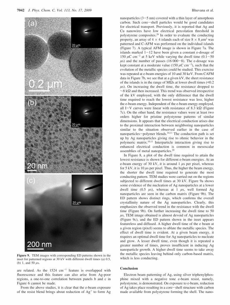
In Figure 8, a plot of the dwell time required to attain thelowest resistance is shown for different e-beam energies. At ane-beam energy of 30 kV, it is around 1 µs per pixel, whereasfor 5 kV, it is 10 µs per pixel. Thus, the higher the beam energy,the shorter the dwell time required to generate the mostconducting pattern. TEM studies were carried out on the regionssubjected to different dwell times at 30 kV. Figure 9a showssome evidence of the nucleation of Ag nanoparticles at a lowerdwell time (0.5 µs), whereas at 1 µs, well formed Agnanoparticles are seen in the carbon matrix (Figure 9b). TheED pattern shows distinct rings, which confirms the overallcrystallinity nature of the Ag nanoparticles. Clearly, thisemphasizes the observed trend in the resistance with the dwelltime (Figure 9b). On further increasing the dwell time to 50µs, TEM image obtained is almost devoid of Ag nanoparticles(Figure 9c), and the ED pattern shown in the inset appearsfeatureless and diffused. A higher dwell time of the e beam ata given region (pixel) seems to ablate the metallic species. Theeffect of dwell time is evident. At a given beam energy, itrequires an optimal dwell time for Ag nanoparticles to nucleateand grow. A lesser dwell time, even though it is repeated agreater number of times, proves insufficient in inducing Agnanoparticle growth. A higher dwell time seems to take awaythe metallic species leaving behind only carbon-based matrix,which is less conducting.
Conclusion
Electron beam patterning of Ag, using silver triphenylphos-phine mixed with a negative tone e-beam resist, namely,polystyrene, is demonstrated. On exposure to e-beam, reductionof Ag takes place resulting in a core-shell structure with carbonmade available from polystyrene forming the shell. The nano-
Figure 9. TEM images with corresponding ED patterns shown in theinset for patterned regions at 30 kV with different dwell times (a) 0.5,(b) 1, and 50 µs.
7042 J. Phys. Chem. C, Vol. 113, No. 17, 2009 Bhuvana et al.
particles are of 5-50 nm in size and form bigger aggregates.The reduction of Ag was also confirmed by XPS measurementswhich showed the presence of Ag0 peaks at 367.2 and 373.1eV while UV-vis spectra showed a peak around 464 nm,characteristics of surface plasmon absorption of Ag nanopar-ticles. The Ag-carbon core shell structures exhibit fluorescenceproperty. C-AFM studies carried out on the patterned blendsupported the formation of metallised polystyrene with theresistance values two orders better than that of the pristine.Proximal electronic interaction between neighboring nanopar-ticles is believed to be responsible for the electrical conduction.Thus, the study has shown how conducting patterns of poly-styrene can be obtained by doping with Ag nanoparticles grownin situ. The negative resist behavior of polystyrene in combina-tion with the ability of the Ag complex to reduce under e-beamhas been exploited, making the blend a potential electron resistmaterial for conducting patterns.
Acknowledgment. The authors are grateful to ProfessorC. N. R. Rao for his encouragement. Financial support fromthe Department of Science and Technology, Government ofIndia, is gratefully acknowledged. The authors thank Ms. BRadha for technical help.
References and Notes
(1) Chuang, C. M.; Wu, M. C.; Huang, Y. C.; Cheng, K. C.; Lin, C. F.;Chen, Y. F.; Su, W. F. Nanotechnology 2006, 17, 4399.
(2) Abargues, R.; Marques-Hueso, J.; Canet-Ferrer, J.; Pedrueza, E.;Valdes, J. L.; Jimenez, E.; Martinez-Pastor, J. P. Nanotechnology 2008,19, 355308.
(3) Bhuvana, T.; Kulkarni, G. U. ACS Nano 2008, 2, 457.(4) Ochiai, Y.; Manako, S.; Fujita, J. i.; Nomura, E. J. Vacuum Sci.
Technol. B 1999, 17, 933.
(5) Bogle, K. A.; Dhole, S. D.; Bhoraskar, V. N. Nanotechnology 2006,17, 3204.
(6) Mahapatra, S. K.; Bogle, K. A.; Dhole, S. D.; Bhoraskar, V. N.Nanotechnology 2007, 18, 135602.
(7) Eilers, H.; Biswas, A.; Pounds, T. D.; Norton, M. G.; Elbahri, M.J. Mater. Res. 2006, 21, 2168.
(8) Porel, S.; Singh, S.; Harsha, S. S.; Rao, D. N.; Radhakrishnan, T. P.Chem. Mater. 2005, 17, 9.
(9) Deshmukh, R. D.; Composto, R. J. Chem. Mater. 2007, 19, 745.(10) Basak, D.; Karan, S.; Mallik, B. Chem. Phys. Lett. 2006, 420, 115.(11) Basak, D.; Karan, S.; Mallik, B. Solid State Commun. 2007, 141,
483.(12) Khan, M.; Oldhama, C.; Tuck, D. Can. J. Chem. 1981, 59, 2714.(13) Bhuvana, T.; Kulkarni, G. U. Bull. Mater. Sci. 2008, 31, 201.(14) Austin, M. D.; Zhang, W.; Ge, H.; Wasserman, D.; Lyon, S. A.;
Chou, S. Y. Nanotechnology 2005, 16, 1058.(15) John, N. S.; Kulkarni, G. U. J. Nanosci. Nanotechnol. 2005, 5,
587.(16) Bhuvana, T.; Kulkarni, G. U. Bull. Mater. Sci. 2008, 31, 201–206.(17) Seah, M. P.; Briggs, D. Practical Surface Analysis by Auger and
X-ray Photoelectron Spectroscopy, 2nd ed.; Wiley & Sons: Chichester, U.K.,1992.
(18) Salz, D.; Lamber, R.; Wark, M.; Baalmann, A.; Jaeger, N. Phys.Chem. Chem. Phys. 1999, 1, 4447.
(19) Rao, C. N. R.; Thomas, P. J.; Kulkarni G. U. Nanocrystals:Synthesis, Properties and Applications; Springer-Verlag: Berlin, 2007.
(20) Agrawal, V. V.; Kulkarni, G. U.; Rao, C. N. R. J. Phys. Chem. B2005, 109, 7300.
(21) Farcau, C. A.; Astilean, S. J. Optoelectron. AdV. Mater. 2005, 7,2721.
(22) Subramaniam, C.; Sreeprasad, T. S.; Pradeep, T.; Pavan Kumar,G. V.; Narayana, C.; Yajima, T.; Sugawara, Y.; Tanaka, H.; Ogawa, T.;Chakrabarti, J. Phys. ReV. Lett. 2007, 99, 167404.
(23) Zhang, J.; Fu, Y.; Chowdhury, M. H.; Lakowicz, J. R. Nano Lett.2007, 7, 2101.
(24) Ferrari, A. C.; Robertson, J. Phys. ReV. B 2000, 61, 14095.(25) Flouttard, J. L.; Akinnifesi, J.; Cambril, E.; Despax, B. J. Appl.
Phys. 1991, 70, 798.(26) Gelves, G. A.; Lin, B.; Sundararaj, U.; Haber, J. A. AdV. Funct.
Mater. 2006, 16, 2423.
JP811062M
Ag Complex-Polystyrene Blend as an e-Beam Resist J. Phys. Chem. C, Vol. 113, No. 17, 2009 7043