Embed Size (px)
Citation preview
A full die photograph of the MIPS R2000 RISC Microprocessor is shown above. The 1986 MIPS R2000 with five pipeline stages and 450,000 transistors was the world’s first commercial RISC microprocessor. Photograph ©1995-2004 courtesy of Michael Davidson, Florida State University.
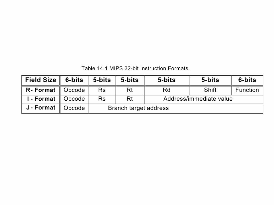
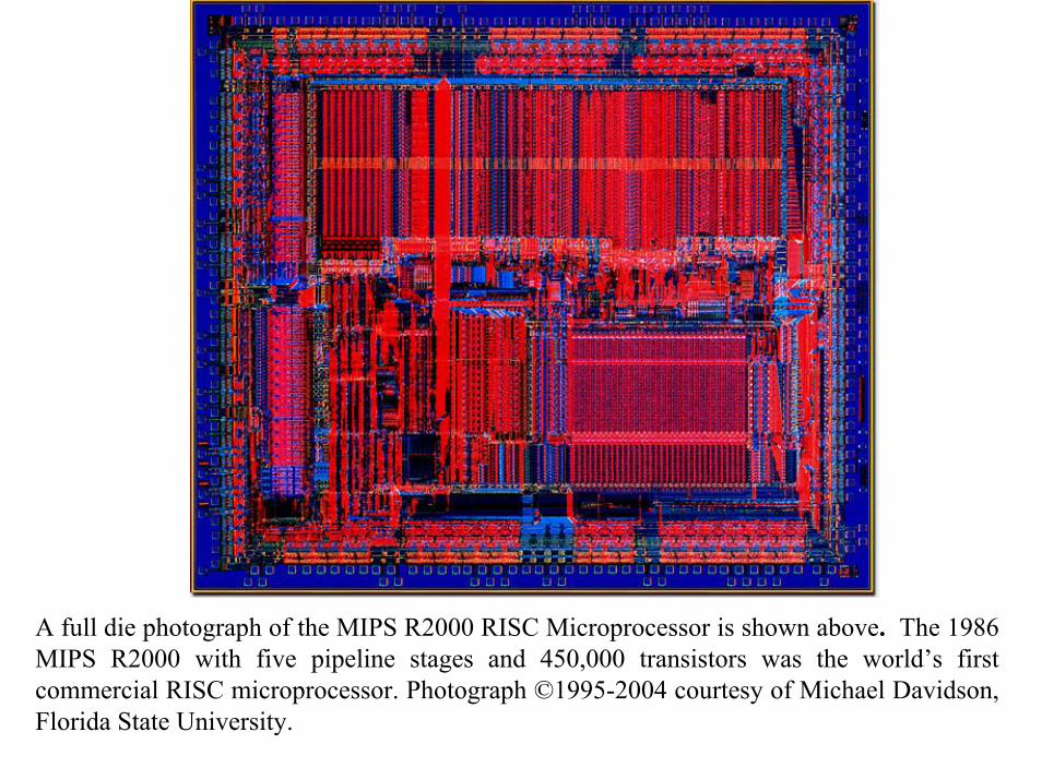
Table 14.1 MIPS 32-bit Instruction Formats.
Field Size 6-bits 5-bits 5-bits 5-bits 5-bits 6-bits R - Format Opcode Rs Rt Rd Shift Function I - Format Opcode Rs Rt Address/immediate value J - Format Opcode Branch target address
LW $2, B ;Register 2 = value of memory at address BLW $3, C ;Register 3 = value of memory at address CADD $4, $2, $3 ;Register 4 = B + C SW $4, A ;Value of memory at address A = Register 4
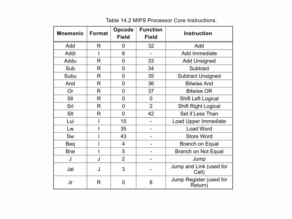
Table 14.2 MIPS Processor Core Instructions.
Mnemonic FormatOpcode
Field Function
Field Instruction
Add R 0 32 Add Addi I 8 - Add Immediate Addu R 0 33 Add Unsigned Sub R 0 34 Subtract
Subu R 0 35 Subtract Unsigned And R 0 36 Bitwise And Or R 0 37 Bitwise OR Sll R 0 0 Shift Left Logical Srl R 0 2 Shift Right Logical Slt R 0 42 Set if Less Than Lui I 15 - Load Upper Immediate Lw I 35 - Load Word Sw I 43 - Store Word Beq I 4 - Branch on Equal Bne I 5 - Branch on Not Equal
J J 2 - Jump
Jal J 3 - Jump and Link (used for Call)
Jr R 0 8 Jump Register (used for Return)
4
PCReadAddress
InstructionMemory
Instruction[31-0]
Instruction[31-26] Control
Unit
RegDstBranchMemReadMemtoRegALUOpMemWriteALUSrcRegWrite
Instruction[25-21]
Instruction[20-16]
Instruction[15-11]
Instruction[15-0]
ReadRegister 1
ReadRegister 2
WriteRegister
WriteData
ReadData 1
ReadData 2
Zero
ALUResult
ADDADD
ResultShiftLeft
2
Address
WriteData
DataMemory
ReadData
ADD
SignExtend
16 32
ALUControlInstruction
[5-0]
0
1
Mux
1
0
Mux
0
1
Mux
0
1
Mux
Registers
PC + 4
ALU
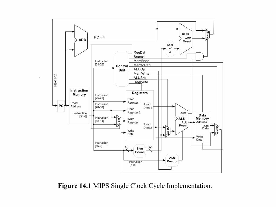
Figure 14.1 MIPS Single Clock Cycle Implementation.
PC Address
InstructionMemory
Control
Instruction[15-0]
ReadRegister 1
ReadRegister 2
WriteRegister
WriteData
ReadData 1
ReadData 2
ALU
Zero
ALUResult
ShiftLeft
2
Address
WriteData
DataMemory
ReadData
ADD
4
SignExtend
16 32 ALUControl
1
0
Mux
0
1
Mux
Registers
Instruction[20-16]Instruction[15-11]
Pipeline
Register
ADDADD
Result
0
1
Mux
6
WB
M
EX
Pipeline
Register
Pipeline
Register
PCSrc
ID/EX
0
1
Mux
ALUOp
RegDst
ALUSrc
WB
M
EX/MEM
Pipeline
Register
WB
MEM/WB
Branch
MemRead
IF/ID
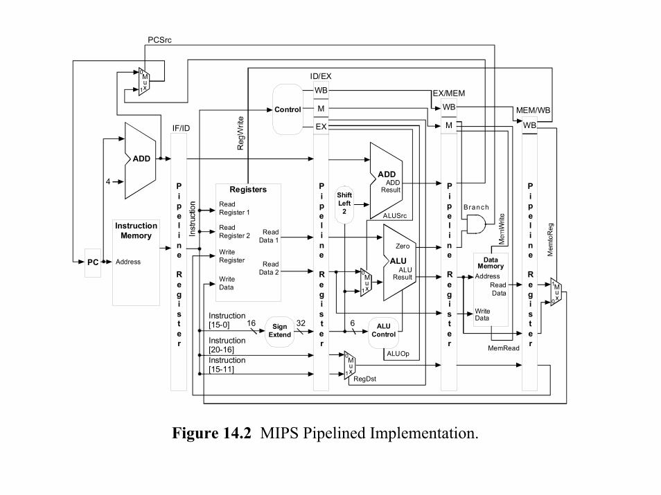
Figure 14.2 MIPS Pipelined Implementation.

-- Top Level Structural Model for MIPS Processor CoreLIBRARY IEEE;USE IEEE.STD_LOGIC_1164.ALL;USE IEEE.STD_LOGIC_ARITH.ALL;ENTITY MIPS IS
PORT( reset, clock : IN STD_LOGIC; -- Output important signals to pins for easy display in SimulatorPC : OUT STD_LOGIC_VECTOR( 7 DOWNTO 0 );ALU_result_out, read_data_1_out, read_data_2_out, write_data_out, Instruction_out : OUT STD_LOGIC_VECTOR( 31 DOWNTO 0 );Branch_out, Zero_out, Memwrite_out, Regwrite_out : OUT STD_LOGIC );
END TOP_SPIM;ARCHITECTURE structure OF TOP_SPIM IS
COMPONENT IfetchPORT( Instruction : OUT STD_LOGIC_VECTOR( 31 DOWNTO 0 );
PC_plus_4_out : OUT STD_LOGIC_VECTOR( 9 DOWNTO 0 );Add_result : IN STD_LOGIC_VECTOR( 7 DOWNTO 0 );Branch : IN STD_LOGIC;Zero : IN STD_LOGIC;PC_out : OUT STD_LOGIC_VECTOR( 9 DOWNTO 0 );clock,reset : IN STD_LOGIC );
END COMPONENT;
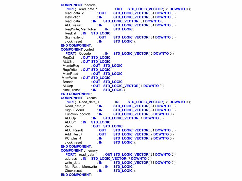
COMPONENT IdecodePORT( read_data_1 : OUT STD_LOGIC_VECTOR( 31 DOWNTO 0 );read_data_2 : OUT STD_LOGIC_VECTOR( 31 DOWNTO 0 );Instruction : IN STD_LOGIC_VECTOR( 31 DOWNTO 0 );read_data : IN STD_LOGIC_VECTOR( 31 DOWNTO 0 );ALU_result : IN STD_LOGIC_VECTOR( 31 DOWNTO 0 );RegWrite, MemtoReg : IN STD_LOGIC;RegDst : IN STD_LOGIC;Sign_extend : OUT STD_LOGIC_VECTOR( 31 DOWNTO 0 );clock, reset : IN STD_LOGIC );
END COMPONENT;COMPONENT control
PORT( Opcode : IN STD_LOGIC_VECTOR( 5 DOWNTO 0 );RegDst : OUT STD_LOGIC;ALUSrc : OUT STD_LOGIC;MemtoReg : OUT STD_LOGIC;RegWrite : OUT STD_LOGIC;MemRead : OUT STD_LOGIC;MemWrite : OUT STD_LOGIC;Branch : OUT STD_LOGIC;ALUop : OUT STD_LOGIC_VECTOR( 1 DOWNTO 0 );clock, reset : IN STD_LOGIC );
END COMPONENT;COMPONENT Execute
PORT( Read_data_1 : IN STD_LOGIC_VECTOR( 31 DOWNTO 0 );Read_data_2 : IN STD_LOGIC_VECTOR( 31 DOWNTO 0 );Sign_Extend : IN STD_LOGIC_VECTOR( 31 DOWNTO 0 );Function_opcode : IN STD_LOGIC_VECTOR( 5 DOWNTO 0 );ALUOp : IN STD_LOGIC_VECTOR( 1 DOWNTO 0 );ALUSrc : IN STD_LOGIC;Zero : OUT STD_LOGIC;ALU_Result : OUT STD_LOGIC_VECTOR( 31 DOWNTO 0 );Add_Result : OUT STD_LOGIC_VECTOR( 7 DOWNTO 0 );PC_plus_4 : IN STD_LOGIC_VECTOR( 9 DOWNTO 0 );clock, reset : IN STD_LOGIC );
END COMPONENT;COMPONENT dmemory
PORT( read_data : OUT STD_LOGIC_VECTOR( 31 DOWNTO 0 );address : IN STD_LOGIC_VECTOR( 7 DOWNTO 0 );write_data : IN STD_LOGIC_VECTOR( 31 DOWNTO 0 );MemRead, Memwrite : IN STD_LOGIC;Clock,reset : IN STD_LOGIC );
END COMPONENT;
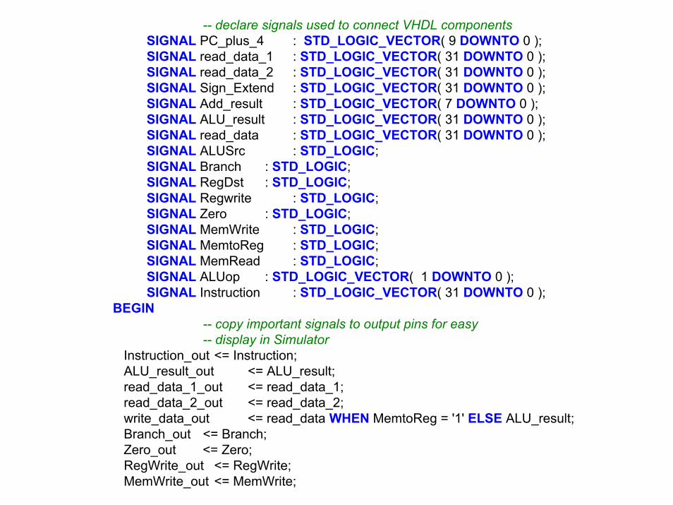
-- declare signals used to connect VHDL componentsSIGNAL PC_plus_4 : STD_LOGIC_VECTOR( 9 DOWNTO 0 );SIGNAL read_data_1 : STD_LOGIC_VECTOR( 31 DOWNTO 0 );SIGNAL read_data_2 : STD_LOGIC_VECTOR( 31 DOWNTO 0 );SIGNAL Sign_Extend : STD_LOGIC_VECTOR( 31 DOWNTO 0 );SIGNAL Add_result : STD_LOGIC_VECTOR( 7 DOWNTO 0 );SIGNAL ALU_result : STD_LOGIC_VECTOR( 31 DOWNTO 0 );SIGNAL read_data : STD_LOGIC_VECTOR( 31 DOWNTO 0 );SIGNAL ALUSrc : STD_LOGIC;SIGNAL Branch : STD_LOGIC;SIGNAL RegDst : STD_LOGIC;SIGNAL Regwrite : STD_LOGIC;SIGNAL Zero : STD_LOGIC;SIGNAL MemWrite : STD_LOGIC;SIGNAL MemtoReg : STD_LOGIC;SIGNAL MemRead : STD_LOGIC;SIGNAL ALUop : STD_LOGIC_VECTOR( 1 DOWNTO 0 );SIGNAL Instruction : STD_LOGIC_VECTOR( 31 DOWNTO 0 );
BEGIN-- copy important signals to output pins for easy -- display in Simulator
Instruction_out <= Instruction;ALU_result_out <= ALU_result;read_data_1_out <= read_data_1;read_data_2_out <= read_data_2;write_data_out <= read_data WHEN MemtoReg = '1' ELSE ALU_result;Branch_out <= Branch;Zero_out <= Zero;RegWrite_out <= RegWrite;MemWrite_out <= MemWrite;
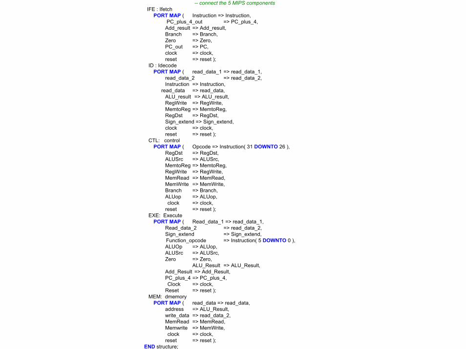
-- connect the 5 MIPS components IFE : Ifetch
PORT MAP ( Instruction => Instruction,PC_plus_4_out => PC_plus_4,
Add_result => Add_result,Branch => Branch,Zero => Zero,PC_out => PC, clock => clock, reset => reset );
ID : IdecodePORT MAP ( read_data_1 => read_data_1,
read_data_2 => read_data_2,Instruction => Instruction,
read_data => read_data,ALU_result => ALU_result,RegWrite => RegWrite,MemtoReg => MemtoReg,RegDst => RegDst,Sign_extend => Sign_extend,clock => clock, reset => reset );
CTL: controlPORT MAP ( Opcode => Instruction( 31 DOWNTO 26 ),
RegDst => RegDst,ALUSrc => ALUSrc,MemtoReg => MemtoReg,RegWrite => RegWrite,MemRead => MemRead,MemWrite => MemWrite,Branch => Branch,ALUop => ALUop,clock => clock,
reset => reset );EXE: Execute
PORT MAP ( Read_data_1 => read_data_1,Read_data_2 => read_data_2,Sign_extend => Sign_extend,Function_opcode => Instruction( 5 DOWNTO 0 ),ALUOp => ALUop,ALUSrc => ALUSrc,Zero => Zero,
ALU_Result => ALU_Result,Add_Result => Add_Result,PC_plus_4 => PC_plus_4,Clock => clock,
Reset => reset );MEM: dmemory
PORT MAP ( read_data => read_data,address => ALU_Result,write_data => read_data_2,MemRead => MemRead, Memwrite => MemWrite, clock => clock,
reset => reset );END structure;
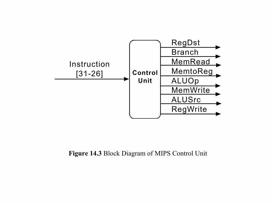
Instruction[31-26] Control
Unit
RegDstBranchMemReadMemtoRegALUOpMemWriteALUSrcRegWrite
Figure 14.3 Block Diagram of MIPS Control Unit
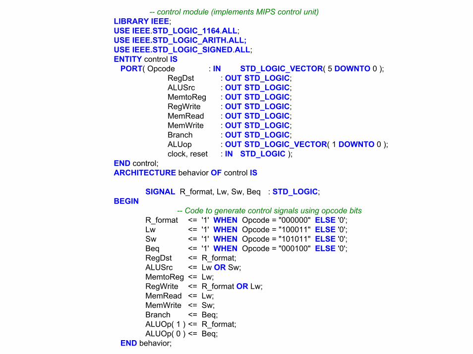
-- control module (implements MIPS control unit)LIBRARY IEEE;USE IEEE.STD_LOGIC_1164.ALL;USE IEEE.STD_LOGIC_ARITH.ALL;USE IEEE.STD_LOGIC_SIGNED.ALL;ENTITY control IS
PORT( Opcode : IN STD_LOGIC_VECTOR( 5 DOWNTO 0 );RegDst : OUT STD_LOGIC;ALUSrc : OUT STD_LOGIC;MemtoReg : OUT STD_LOGIC;RegWrite : OUT STD_LOGIC;MemRead : OUT STD_LOGIC;MemWrite : OUT STD_LOGIC;Branch : OUT STD_LOGIC;ALUop : OUT STD_LOGIC_VECTOR( 1 DOWNTO 0 );clock, reset : IN STD_LOGIC );
END control;ARCHITECTURE behavior OF control IS
SIGNAL R_format, Lw, Sw, Beq : STD_LOGIC;BEGIN
-- Code to generate control signals using opcode bitsR_format <= '1' WHEN Opcode = "000000" ELSE '0';Lw <= '1' WHEN Opcode = "100011" ELSE '0';Sw <= '1' WHEN Opcode = "101011" ELSE '0';Beq <= '1' WHEN Opcode = "000100" ELSE '0';RegDst <= R_format;ALUSrc <= Lw OR Sw;MemtoReg <= Lw;RegWrite <= R_format OR Lw;MemRead <= Lw;MemWrite <= Sw; Branch <= Beq;ALUOp( 1 ) <= R_format;ALUOp( 0 ) <= Beq;
END behavior;

0
1
Mux
PC ReadAddress
InstructionMemory
Instruction[31-0]
NextPC
Clock
ADD Result
ZeroBranch
PC + 4ADD
4
Figure 14.4 Block Diagram of MIPS Fetch Unit.

-- Ifetch module (provides the PC and instruction --memory for the MIPS computer)
LIBRARY IEEE;USE IEEE.STD_LOGIC_1164.ALL;USE IEEE.STD_LOGIC_ARITH.ALL;USE IEEE.STD_LOGIC_UNSIGNED.ALL;LIBRARY altera_mf;USE altera_mf.altera_mf_components.ALL;ENTITY Ifetch IS
PORT( SIGNAL Instruction : OUT STD_LOGIC_VECTOR( 31 DOWNTO 0 );SIGNAL PC_plus_4_out : OUT STD_LOGIC_VECTOR( 7 DOWNTO 0 );
SIGNAL Add_result : IN STD_LOGIC_VECTOR( 7 DOWNTO 0 );SIGNAL Branch : IN STD_LOGIC;SIGNAL Zero : IN STD_LOGIC;
SIGNAL PC_out : OUTSTD_LOGIC_VECTOR( 9 DOWNTO 0 );SIGNAL clock, reset : IN STD_LOGIC);
END Ifetch;ARCHITECTURE behavior OF Ifetch IS
SIGNAL PC, PC_plus_4 : STD_LOGIC_VECTOR( 9 DOWNTO 0 );SIGNAL next_PC : STD_LOGIC_VECTOR( 7 DOWNTO 0 );
BEGIN--ROM for Instruction Memory
data_memory: altsyncram
GENERIC MAP ( operation_mode => "ROM",width_a => 32,widthad_a => 8,lpm_type => "altsyncram",outdata_reg_a => "UNREGISTERED",
-- Reads in mif file for initial data memory valuesinit_file => "program.mif",intended_device_family => "Cyclone")
-- Fetch next instruction from memory using PCPORT MAP (
clock0 => clock,address_a => Mem_Addr, q_a => Instruction );
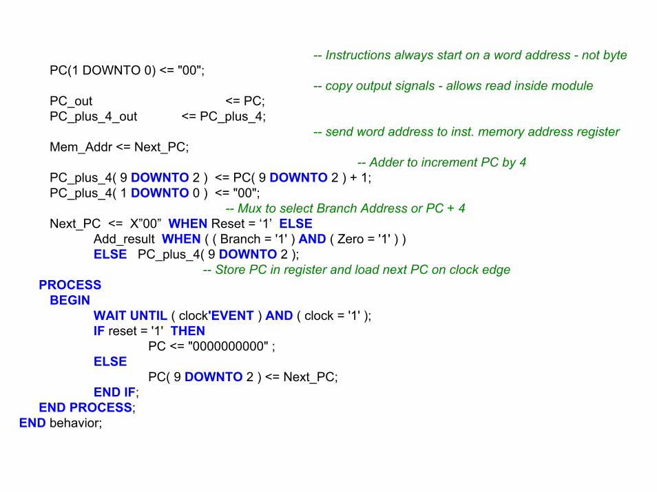
-- Instructions always start on a word address - not bytePC(1 DOWNTO 0) <= "00";
-- copy output signals - allows read inside modulePC_out <= PC;PC_plus_4_out <= PC_plus_4;
-- send word address to inst. memory address registerMem_Addr <= Next_PC;
-- Adder to increment PC by 4 PC_plus_4( 9 DOWNTO 2 ) <= PC( 9 DOWNTO 2 ) + 1;PC_plus_4( 1 DOWNTO 0 ) <= "00";
-- Mux to select Branch Address or PC + 4 Next_PC <= X”00” WHEN Reset = ‘1’ ELSE
Add_result WHEN ( ( Branch = '1' ) AND ( Zero = '1' ) ) ELSE PC_plus_4( 9 DOWNTO 2 );
-- Store PC in register and load next PC on clock edgePROCESS
BEGINWAIT UNTIL ( clock'EVENT ) AND ( clock = '1' );IF reset = '1' THEN
PC <= "0000000000" ; ELSE
PC( 9 DOWNTO 2 ) <= Next_PC;END IF;
END PROCESS;END behavior;

-- MIPS Instruction Memory Initialization FileDepth = 256;Width = 32;Address_radix = HEX;Data_radix = HEX;ContentBegin
-- Use NOPS for default instruction memory values[00..FF]: 00000000; -- nop (sll r0,r0,0)
-- Place MIPS Instructions here-- Note: memory addresses are in words and not bytes-- i.e. next location is +1 and not +4
00: 8C020000; -- lw $2,0 ;memory(00)=5501: 8C030001; -- lw $3,1 ;memory(01)=AA02: 00430820; -- add $1,$2,$303: AC010003; -- sw $1,3 ;memory(03)=FF04: 1022FFFF; -- beq $1,$2,-405: 1021FFFA; -- beq $1,$1,-24
End;
Figure 14.5 MIPS Program Memory Initialization File, program.mif.

Read Data
Instruction[25 - 21]
Instruction[20 - 16]
Instruction[15 - 11]
ReadRegister 1
ReadRegister 2
WriteRegister
WriteData
ReadData 1
ReadData 2
0
1
Mux
Registers
Instruction[15 - 0] Sign
Extend16 32
0
1
Mux
ALU Result
MemtoReg
RegWriteRegDst
Figure 14.6 Block Diagram of MIPS Decode Unit.
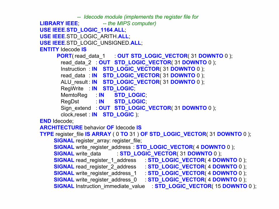
-- Idecode module (implements the register file forLIBRARY IEEE; -- the MIPS computer)USE IEEE.STD_LOGIC_1164.ALL;USE IEEE.STD_LOGIC_ARITH.ALL;USE IEEE.STD_LOGIC_UNSIGNED.ALL;ENTITY Idecode IS
PORT( read_data_1 : OUT STD_LOGIC_VECTOR( 31 DOWNTO 0 );read_data_2 : OUT STD_LOGIC_VECTOR( 31 DOWNTO 0 );Instruction : IN STD_LOGIC_VECTOR( 31 DOWNTO 0 );read_data : IN STD_LOGIC_VECTOR( 31 DOWNTO 0 );ALU_result : IN STD_LOGIC_VECTOR( 31 DOWNTO 0 );RegWrite : IN STD_LOGIC;MemtoReg : IN STD_LOGIC;RegDst : IN STD_LOGIC;Sign_extend : OUT STD_LOGIC_VECTOR( 31 DOWNTO 0 );clock,reset : IN STD_LOGIC );
END Idecode;ARCHITECTURE behavior OF Idecode ISTYPE register_file IS ARRAY ( 0 TO 31 ) OF STD_LOGIC_VECTOR( 31 DOWNTO 0 );
SIGNAL register_array: register_file;SIGNAL write_register_address : STD_LOGIC_VECTOR( 4 DOWNTO 0 );SIGNAL write_data : STD_LOGIC_VECTOR( 31 DOWNTO 0 );SIGNAL read_register_1_address : STD_LOGIC_VECTOR( 4 DOWNTO 0 );SIGNAL read_register_2_address : STD_LOGIC_VECTOR( 4 DOWNTO 0 );SIGNAL write_register_address_1 : STD_LOGIC_VECTOR( 4 DOWNTO 0 );SIGNAL write_register_address_0 : STD_LOGIC_VECTOR( 4 DOWNTO 0 );SIGNAL Instruction_immediate_value : STD_LOGIC_VECTOR( 15 DOWNTO 0 );
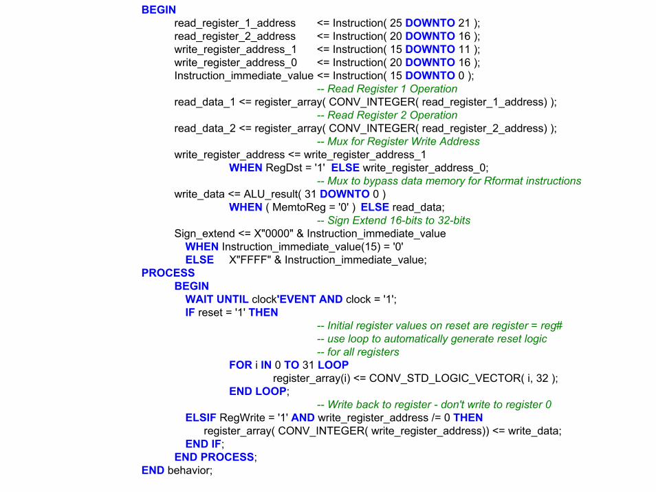
BEGINread_register_1_address <= Instruction( 25 DOWNTO 21 );read_register_2_address <= Instruction( 20 DOWNTO 16 );write_register_address_1 <= Instruction( 15 DOWNTO 11 );write_register_address_0 <= Instruction( 20 DOWNTO 16 );Instruction_immediate_value <= Instruction( 15 DOWNTO 0 );
-- Read Register 1 Operationread_data_1 <= register_array( CONV_INTEGER( read_register_1_address) );
-- Read Register 2 Operationread_data_2 <= register_array( CONV_INTEGER( read_register_2_address) );
-- Mux for Register Write Addresswrite_register_address <= write_register_address_1
WHEN RegDst = '1' ELSE write_register_address_0;-- Mux to bypass data memory for Rformat instructions
write_data <= ALU_result( 31 DOWNTO 0 ) WHEN ( MemtoReg = '0' ) ELSE read_data;
-- Sign Extend 16-bits to 32-bitsSign_extend <= X"0000" & Instruction_immediate_value
WHEN Instruction_immediate_value(15) = '0'ELSE X"FFFF" & Instruction_immediate_value;
PROCESSBEGIN
WAIT UNTIL clock'EVENT AND clock = '1';IF reset = '1' THEN
-- Initial register values on reset are register = reg#-- use loop to automatically generate reset logic -- for all registers
FOR i IN 0 TO 31 LOOPregister_array(i) <= CONV_STD_LOGIC_VECTOR( i, 32 );
END LOOP;-- Write back to register - don't write to register 0
ELSIF RegWrite = '1' AND write_register_address /= 0 THENregister_array( CONV_INTEGER( write_register_address)) <= write_data;
END IF;END PROCESS;
END behavior;
2
1Z e r o
A L U Re s u l t
0
1
Mux
AL U
ADD A D D
Re s u l t ShiftLeft
2
PC+4
SignExtend
ReadData
SignExtend
ReadData
ALUControlALUOP
ALUSrc
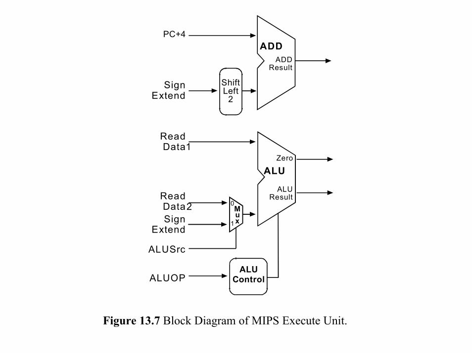
Figure 13.7 Block Diagram of MIPS Execute Unit.
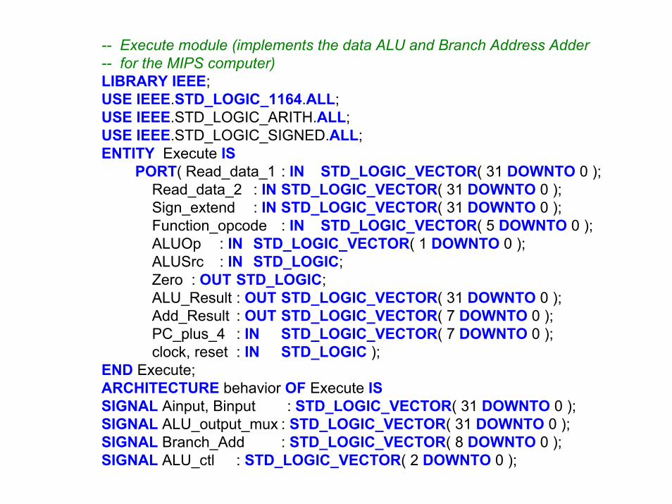
-- Execute module (implements the data ALU and Branch Address Adder -- for the MIPS computer)LIBRARY IEEE;USE IEEE.STD_LOGIC_1164.ALL;USE IEEE.STD_LOGIC_ARITH.ALL;USE IEEE.STD_LOGIC_SIGNED.ALL;ENTITY Execute IS
PORT( Read_data_1 : IN STD_LOGIC_VECTOR( 31 DOWNTO 0 );Read_data_2 : IN STD_LOGIC_VECTOR( 31 DOWNTO 0 );Sign_extend : IN STD_LOGIC_VECTOR( 31 DOWNTO 0 );Function_opcode : IN STD_LOGIC_VECTOR( 5 DOWNTO 0 );ALUOp : IN STD_LOGIC_VECTOR( 1 DOWNTO 0 );ALUSrc : IN STD_LOGIC;Zero : OUT STD_LOGIC;ALU_Result : OUT STD_LOGIC_VECTOR( 31 DOWNTO 0 );Add_Result : OUT STD_LOGIC_VECTOR( 7 DOWNTO 0 );PC_plus_4 : IN STD_LOGIC_VECTOR( 7 DOWNTO 0 );clock, reset : IN STD_LOGIC );
END Execute;ARCHITECTURE behavior OF Execute ISSIGNAL Ainput, Binput : STD_LOGIC_VECTOR( 31 DOWNTO 0 );SIGNAL ALU_output_mux : STD_LOGIC_VECTOR( 31 DOWNTO 0 );SIGNAL Branch_Add : STD_LOGIC_VECTOR( 8 DOWNTO 0 );SIGNAL ALU_ctl : STD_LOGIC_VECTOR( 2 DOWNTO 0 );
BEGINAinput <= Read_data_1;
-- ALU input muxBinput <= Read_data_2
WHEN ( ALUSrc = '0' ) ELSE Sign_extend( 31 DOWNTO 0 );
-- Generate ALU control bitsALU_ctl( 0 ) <= ( Function_opcode( 0 ) OR Function_opcode( 3 ) ) AND ALUOp(1 );ALU_ctl( 1 ) <= ( NOT Function_opcode( 2 ) ) OR (NOT ALUOp( 1 ) );ALU_ctl( 2 ) <= ( Function_opcode( 1 ) AND ALUOp( 1 )) OR ALUOp( 0 );
-- Generate Zero FlagZero <= '1'
WHEN ( ALU_output_mux( 31 DOWNTO 0 ) = X"00000000" )ELSE '0';
-- Select ALU output for SLT ALU_result <= X"0000000" & B"000" & ALU_output_mux( 31 )
WHEN ALU_ctl = "111" ELSE ALU_output_mux( 31 DOWNTO 0 );
-- Adder to compute Branch AddressBranch_Add <= PC_plus_4( 9 DOWNTO 2 ) + Sign_extend( 7 DOWNTO 0 ) ;Add_result <= Branch_Add( 7 DOWNTO 0 );
PROCESS ( ALU_ctl, Ainput, Binput )BEGIN
-- Select ALU operationCASE ALU_ctl IS
-- ALU performs ALUresult = A_input AND B_inputWHEN "000" => ALU_output_mux <= Ainput AND Binput;
-- ALU performs ALUresult = A_input OR B_inputWHEN "001" => ALU_output_mux <= Ainput OR Binput;
-- ALU performs ALUresult = A_input + B_inputWHEN "010" => ALU_output_mux <= Ainput + Binput;
-- ALU performs ?WHEN "011" => ALU_output_mux <= X”00000000” ;
-- ALU performs ?WHEN "100" => ALU_output_mux <= X"00000000" ;
-- ALU performs ?WHEN "101" => ALU_output_mux <= X"00000000" ;
-- ALU performs ALUresult = A_input - B_inputWHEN "110" => ALU_output_mux <= Ainput - Binput;
-- ALU performs SLTWHEN "111" => ALU_output_mux <= Ainput - Binput ;WHEN OTHERS => ALU_output_mux <= X"00000000" ;
END CASE;END PROCESS;END behavior;
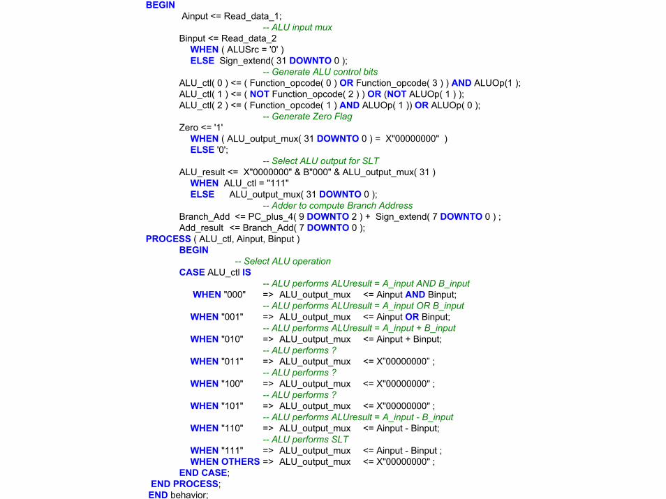
Address
WriteData
DataMemory
ReadData
MemWrite
MemRead
Figure 14.8 Block Diagram of MIPS Data Memory Unit.

-- Dmemory module (implements the data-- memory for the MIPS computer)LIBRARY IEEE;USE IEEE.STD_LOGIC_1164.ALL;USE IEEE.STD_LOGIC_ARITH.ALL;USE IEEE.STD_LOGIC_SIGNED.ALL;LIBRARY altera_mf;USE altera_mf.atlera_mf_components.ALL;ENTITY dmemory IS
PORT( read_data : OUT STD_LOGIC_VECTOR( 31 DOWNTO 0 );address : IN STD_LOGIC_VECTOR( 7 DOWNTO 0 );write_data : IN STD_LOGIC_VECTOR( 31 DOWNTO 0 );
MemRead, Memwrite : IN STD_LOGIC;clock, reset : IN STD_LOGIC );
END dmemory;ARCHITECTURE behavior OF dmemory ISSIGNAL write_clock : STD_LOGIC;BEGIN
data_memory: altsyncramGENERIC MAP (
operation_mode => "SINGLE_PORT",width_a => 32,widthad_a => 8,lpm_type => "altsyncram",outdata_reg_a => "UNREGISTERED",
-- Reads in mif file for initial data memory valuesinit_file => "dmemory.mif",intended_device_family => "Cyclone"lpm_widthad => 8
)PORT MAP (
wren_a => memwrite,clock0 => write_clock,address_a => address,data_a => write_data,q_a => read_data );
-- Load memory address & data register with write clockwrite_clock <= NOT clock;
END behavior;
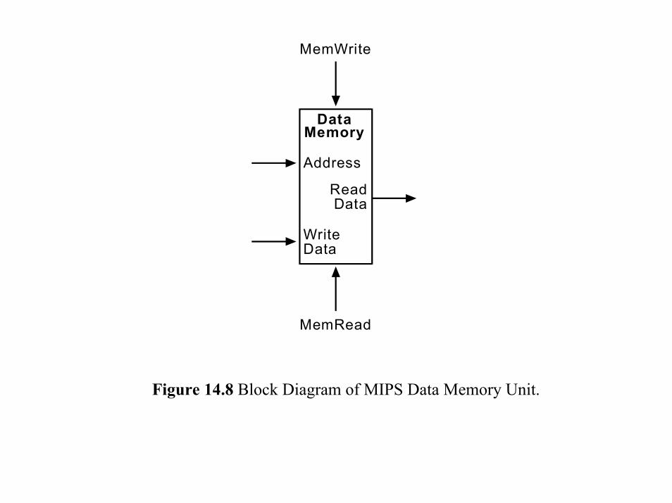
-- MIPS Data Memory Initialization FileDepth = 256;Width = 32;ContentBegin
-- default value for memory[00..FF] : 00000000;
-- initial values for test program00 : 55555555;01 : AAAAAAAA;
End;
Figure 14.9 MIPS Data Memory Initialization File, dmemory.mif.

Figure 14.10 Simulation of MIPS test program.

Figure 14.11 MIPS with Video Output generated by UP 1 Board.