Embed Size (px)
Citation preview

1

TABLE OF CONTENTS
PMI NEW RESEARCH & DEVELOPMENT PRESENTATIONMULTIFUCTION MODULES, SUBSYSTEMS & INTEGRATED ASSEMBLIES
1 Integrated MIC/MMIC Modules 3
2 Form, Fit & Function Products 60
3 IFMs & Frequency Discriminators 62
4 Rack & Chassis Mount Products 65
5 UP & Down Converters, Receiver Front Ends & Transceivers 68
6 Single Sideband Modulators 83
7 Switch Matrices 88
2

1 - INTEGRATED MIC/MMIC MODULES
3

Model No. MPC-20R2G21R2G-CD-LNF20.2 to 21.2 GHz, Monopulse Comparator
• Frequency 20.2 to 21.2 GHz• Lossless from Input to Output• Designed for 100K Noise Temperature• Phase Tracking all 8 Inputs
4
Frequency 20.2 - 21.2 GHz
Gain 0 to +10 dB
Noise Temperature 100 K
Phase Balance ±3° Maximum
DC Supply +12 to +15 VDC Typ.
Control Signal TTL Logic
Connectors SMA (F)
Finish Painted Gray
Size 6.25” x Ø4.80” x 2.00”

Section 1• 8 Antenna Inputs• Phase Matched LNAs• Hybrid Tee• Ringline Couplers• Phase Matched Outputs
Section 2• Hybrid 90° Power Divider• Branchline Coupler• SPDT Absorptive Switch• Solid State
5
Model No. MPC-20R2G21R2G-CD-LNF20.2 to 21.2 GHz, Monopulse Comparator
6
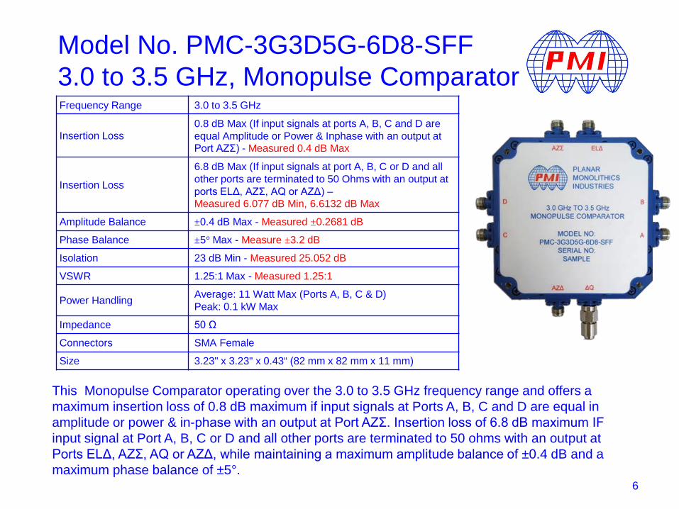
Model No. PMC-3G3D5G-6D8-SFF3.0 to 3.5 GHz, Monopulse Comparator
This Monopulse Comparator operating over the 3.0 to 3.5 GHz frequency range and offers a maximum insertion loss of 0.8 dB maximum if input signals at Ports A, B, C and D are equal in amplitude or power & in-phase with an output at Port AZΣ. Insertion loss of 6.8 dB maximum IF input signal at Port A, B, C or D and all other ports are terminated to 50 ohms with an output at Ports ELΔ, AZΣ, AQ or AZΔ, while maintaining a maximum amplitude balance of ±0.4 dB and a maximum phase balance of ±5°.
Frequency Range 3.0 to 3.5 GHz
Insertion Loss0.8 dB Max (If input signals at ports A, B, C and D are equal Amplitude or Power & Inphase with an output at Port AZΣ) - Measured 0.4 dB Max
Insertion Loss
6.8 dB Max (If input signals at port A, B, C or D and all other ports are terminated to 50 Ohms with an output at ports ELΔ, AZΣ, AQ or AZΔ) –Measured 6.077 dB Min, 6.6132 dB Max
Amplitude Balance ±0.4 dB Max - Measured ±0.2681 dB
Phase Balance ±5° Max - Measure ±3.2 dB
Isolation 23 dB Min - Measured 25.052 dB
VSWR 1.25:1 Max - Measured 1.25:1
Power Handling Average: 11 Watt Max (Ports A, B, C & D)Peak: 0.1 kW Max
Impedance 50 Ω
Connectors SMA Female
Size 3.23" x 3.23" x 0.43“ (82 mm x 82 mm x 11 mm)
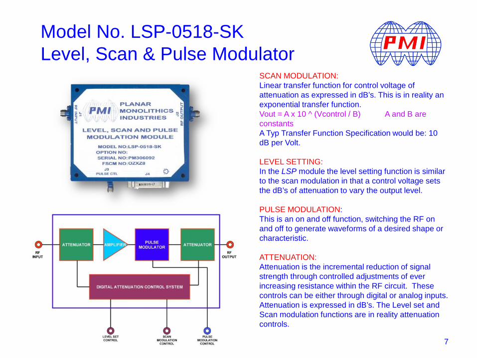
Model No. LSP-0518-SKLevel, Scan & Pulse Modulator
SCAN MODULATION:Linear transfer function for control voltage of attenuation as expressed in dB’s. This is in reality an exponential transfer function.Vout = A x 10 ^ (Vcontrol / B) A and B are constantsA Typ Transfer Function Specification would be: 10 dB per Volt.
LEVEL SETTING:In the LSP module the level setting function is similar to the scan modulation in that a control voltage sets the dB’s of attenuation to vary the output level.
PULSE MODULATION:This is an on and off function, switching the RF on and off to generate waveforms of a desired shape or characteristic.
ATTENUATION:Attenuation is the incremental reduction of signal strength through controlled adjustments of ever increasing resistance within the RF circuit. These controls can be either through digital or analog inputs. Attenuation is expressed in dB’s. The Level set and Scan modulation functions are in reality attenuation controls.
7

8
Model No. LSP-0518-SKLevel, Scan & Pulse Modulator

Model No. PMA-218-LSP0.5 to 18.0 GHz Modulator/Amplifier
9
Frequency Range 0.5 to 18.0 GHzOutput P1 dB +12 dBm MinimumIP3 +22 dBm MinimumRF Input Power +14 dBm Max
+12 dBm OperationalHarmonics at P1 dB -20.0 dBc MinimumSpurious Outputs -60 dBc MinimumVSWR (RF Input) 2.2:1 MaxVSWR (RF Output) 2.2:1 MaxLevel Set (Power Attenuation) 70 dB RangeScan Modulation (Attenuation) 70 dB RangeCombined Attenuation 100 dB MinimumScan and Level Bandwidth 10 kHzScan Pulse Response (Settling) 50 uS MaxScan Pulse Response (Rise/Fall) 15 uS MaxDigital Processing Jitter 10 uS MaxSystem Frequency Flatness ±2 dBAttenuation Frequency Flatness 0-40 dB (±2 dB)
40-60 dB (±3 dB)Attenuation Linearity ±1.5 dBPulse Modulation Depth 60 dB MinimumRF Pulse Width Range 50 ns to CWRF Pulse (Rise Time 10-90%) 9 ns MaxRF Pulse (Fall Time 90-10%) 9 ns MaxRF Pulse Repetition Rate 10 MHz MaxRF Pulse Distortion 0.3 dB MaxPulse / CW Differential 0.4 dB MaxPulse Width Fidelity ±10 ns MaxSensitivity 6 dB/VoltBias Voltages / Currents +15 Vdc @ 1.5 Amps Max
-15 Vdc @ 1.0 Amps MaxSize 4.00" x 3.30" x 0.70"
PMI Model Number PMA-218-LSPis an Analog Level, Scan and Pulse Modulation Module that is capable of exponential (linear in dB) Modulation, for rugged and high reliability applications µsing digital process techniques, that works from 2.0 to 18.0 GHz.

10
Model No. PMA-218-LSP0.5 to 18.0 GHz Modulator/Amplifier

Model No. DGM-18G40G-292FF-DSQuad-Phase & Amplitude Matched Millimeterwave, Diplexer Gain Module
PMI Model No. DGM-18G40G-292FF-DS is a Quad Phase & Amplitude Matched mmW (Millimeter Wave) Diplexer-Gain module designed to operate over the 18.0 to 40 GHz frequency range with a switched output and an integrated power divider feeding the four antenna inputs via a 20 dB coupler for ease of system set up. The band select function not only switches bands, but also allows the amplified bands not in µse to be turned off to reduce power consumption. This model is also designed to have better than 60 dB harmonic suppression.
11
Channel to Channel Performance

12
Model No. DGM-18G40G-292FF-DSQuad-Phase & Amplitude Matched Millimeterwave, Diplexer Gain Module

13
Frequency Range 18.0 to 40.0 GHz
Gain 3 dB min, 7 dB Max - Measured 2.5 to 6.5 dB
Amplitude Ripple
±1.0 dB over every 500 MHz Band starting @ 18.0 GHz, excluding the crossoverMeasured: ±0.68 dB CH1
±0.59 dB CH2 ±0.60 dB CH3±0.51 dB CH4 (Worst Case)
Input P1dB -20 dBm Min - Measured 5 dBm (Worst Case)
Input IP3 -10 dBm, +5 dBm Desired - Measured +3.5 dBm (Worst Case 40 GHz)
Channel to Channel Isolation 50 dB Typ - Measured 49.9 dB
Noise Figure 12 dB Typ - Measured 10 dB
Phase Matching 40 deg. RMS, Channels 2,3,4 to REF. Channel 1, Over Operating TempMeasured 30 Deg. RMS (Worst Case)
Phase Tracking 0.25 deg/ºC Port to Port Typ - Measured 0.22 Deg/C°
mmW/uW Limiter 30 dBm, CW or Pulsed, 2.0 to 40.0 GHz Without Damage, All Inputs - Measured 30 dBm
Limiter 1dB Recovery Time 250 ns - Measured 146 ns
Spurious Products -73 dBm - Measured -74 dBm Measured at Spectrum Analyzer Noise floor
Diplexer K Band 1dB Passband 18.0 GHz Min, 25.0 GHz Max
Diplexer Ka Band 1dB Passband 28.0 GHz Min, 40.0 GHz max
Crossover Band 25.0 GHz min, 28.0 GHz max
Crossover Excess Attenuation 5 dB Typ - Measured 5 dB (Worst Case)
Stopband Attenuation 60 dB - Measured 61 dB (Worst Case)
K Band Stopbands 900 MHz to 15.0 GHz, 32.0 GHz to 46.0 GHz
Ka Band Stopband 900 MHz to 22.0 GHz
Comm Band Attenuation 60 dB - Measured >60 dB
Comm Band 900 MHz to 2.5 GHz
Comm Interference Immunity 36 dBm CW, 900 MHz to 2.5 GHz without Limiter or Amplifier SaturationMeasured 36 dBm Based On filter Rejection
Comm Interference Immunity 53 dBm Pulsed RF, 900 MHz to 2.5 GHz, Without Limiter or Amplifier Saturation Measured 53 dBm Based On filter Rejection
VSWR in Passbands 2.5:1 Typ
Harmonics for -20dBm -80 dBm, 15.0 to 40.0 GHz - Measured -84 dBm
Band Switching Time, Required 1 µs Max, 0.5 µs Typ - Measured 400 ns
Power Divider Input Power 20 dBm Max - Measured 20 dBm
Power Divider Insertion Loss 15 ± 3 dB - Measured 15 dB, ±2 dB
Power Divider Phase Ripple ±5° RMS - Measured ±4 Deg RMS
Band Select Protection Circuitry ±15 V
Power Supply Protection Circuitry on both ±6.0VDC Supplies ±15 V
Power Supply Voltage ±6.0 VDC - Measured +6.0 V @ 0.571 Amps, -6.0 V @ 0.132 Amps
Power Consumption Required 5 W Max - Measured 4.2 W
Connectors 2.92mm (F)
Control Connector (MDM-9PSP) 9 Pin Micro-D Shipped with Mating Connector
Size 3.0" x 8.0" x 0.75"
Model No. DGM-18G40G-292FF-DSQuad-Phase & Amplitude Matched Millimeterwave, Diplexer Gain Module

Model No. PFEM-9D4G-CD-19410 MHz Multi-Function Module
PMI Model No. PFEM-9D4G-CD-1 is a multi-function module that provides amplification, switching and filtering within the frequency band of 9410 MHz. This module provides two input channels and is switchable to a common output. This model is designed to offer multiple gain level selection, high channel to channel isolation and fast switching speeds.
14

SPECIFICATIONS TX (State 1) RX Low Gain (State 2) RX High Gain (State 3)
Max Input Power at J1 0 dBm 14 dBm 14 dBm
Frequency 9410 MHz +/- 3 0MHz 9410 MHz +/- 30 MHz 9410 MHz +/- 30 MHz
Gain 0 to -5 dBm 11 to 15 dBm 30 to 35 dBm
Gain Flatness <0.1 dBm <0.1 dBm <0.1 dBm
Noise Figure N/A 2 dB Nominal, 2.5 dB Max 2 dB Nominal, 2.5 dB Max
VSWR 1.5:1 Typ 1.5:1 Typ 1.5:1 Typ
OP3 (Output) > 18 dBm >18 dBm >18 dBm
OP2 (Output) >8 dBm >8 dBm >8 dBmPort to Port J1-J3 Isolation >85 dB N/A N/A
Max Output Power + 23 dBm
Output Signal Distortion No apparent droop or distortion with a pulse width of 500 to 1000ns, at 500 to 2000 PPS
Video Switching Transients < -120 dBm above 1.7 GHz
Stability Unconditionally stable when terminated at J1, J2 and J3 with short circuit at all phases
Max Out-Of-Band Gain Below In-Band Gain for f > 6.5 GHz-20 dB Below In-Band Gain < 6.5 GHz
Switching Time 50 ns: TX to RX50 ns: RX Low Gain to RX High Gain
Switching Control 3.3 V to 5 V, TTL Compatible
BIAS V/I +12 VDC/ 125 mA Typ
Size 2.89' x 1.62" x 0.63
Finish Painted Gray
15
Model No. PFEM-9D4G-CD-19410 MHz Multi-Function Module

Model No. PEC-18-2R35G-1R75-9-SFF-HS-LMIntegrated Amplifer, Switch, Limiter & Filter Module
PARAMETERS SPECIFICATIONS
CENTER FREQUENCY 2.35 GHz
1dB Bandwidth 150 MHz
≥30 dBc Rejection 2100 and 2600 MHz
Gain (Typ) 18 dB
Noise Figure 1.8 dB Typ2.0 dB Max
Isolation 40 dB Min
VSWR 2.0:1 Max
RF Input Power +30 dBm Max
RF Output Power +2 dBm Max
Switching Speed(On/Off) 100 ns Max
EMI Shielding 60 dB @ 1 Foot Min
Differential Control A > B = “ON”B > A = “OFF”
DC Power Supply +9 VDC
16

17
Model No. PIA-BTFL-GPO-2CHDual Channel Integrated Assembly(Integrated Bias-Tee, Filtered Limiter Module)
PMI model number PIA-BTFL-GPO-2CH is an dual channel integrated assembly that consists of a Bias-Tee, High Pass Filter, and Limiter. This compact module is supplied with field replaceable GPO connectors. The module is designed to be supplied either in hermetic or non-hermetic form. Order Option -HERM for hermetically sealed version.
Passband Lower Limit 2.0 GHz Typ
Passband Upper Limit 19.0 GHz
-3 dB Cut-Off 1.85 GHz Typ
Insertion Loss 2.5 dB Max
Filter Rejection -15 dB Min. @ 1.7 GHz-20 dB Min @ DC to 1.5 GHz
Passband VSWR 1.5:1 Typ, 2.0:1 Max
Bias Rise / Fall Time 50 ns Max (90% to 10%) +12 to -12 V or -12 to +12 V pulses, tr = 1 ns; Rload = 430 Ohms
Limiting Threshold +8 dBm Min
Flat Leakage +20 dBm CW Max+23 dBm Pulsed Max
Pulse Recovery Time 50 ns Max (To within 1 dB of Insertion Loss)
Power Handling 2 W CW Max50W (12usec max. PW, 1% Duty Cycle)
Bias Current ±30 mA Operational (±40 mA Max)
Bias Voltage -12 to +12 VDC
Connectors GPO - Limited Detent
Size 1.5" (L) x 1.5" (W) x 0.4" (H)
Finish MIL-SPEC Epoxy Paint (Gray Color)Mounting Surface to be paint free.
Sealing Epoxy Sealed
Weight 3 ounces Typ

18
Model No. PIA-BTFL-GPO-2CH (Rev B)Dual Channel Integrated Assembly(Integrated Bias-Tee, Filtered Limiter Module)
PMI model number PIA-BTFL-GPO-2CH Revision B is an dual channel integrated assembly that consists of a Bias-Tee, High Pass Filter, and Limiter. This compact module is supplied with field replaceable GPO connectors. The module is hermetically sealed.
Passband Lower Limit 2.0 GHz Typ
Passband Upper Limit 19.0 GHz
-3 dB Cut-Off 1.8 GHz Typical (3 dBc from Insertion Loss measured at 2 GHz)
Insertion Loss 3.0 dB Typ, 3.5 dB Max (2.0 to 19.0 GHz)
Filter Rejection-10 dBc Min @ 1.7 GHz-30 dBc Min @ DC to 1.5 GHz(Referenced to measured Insertion Loss at 2 GHz)
Passband VSWR 2.0:1 Max (3.0 to 19.0 GHz)2.2:1 Max (2.0 to 3.0 GHz)
Bias Rise / Fall Time50 ns Max (90% to 10%) +12 to -12 V or -12 to +12 V pulses, tr = 1 ns; Rload = 430 Ohms
Limiting Threshold +8 dBm Min
Flat Leakage +20 dBm CW Max+23 dBm Pulsed Max
Pulse Recovery Time 50 ns Max (To within 1 dB of Insertion Loss)
Cross Channel Isolation -73 dB Min
2nd Order Input Intercept Point +30 dB Min (-15 dBm Tones)
3rd Order Input Intercept Point +17dB Min (-15 dBm Tones)
Power Handling 1 W CW Max20 W ( 20% Duty Cycle)
Bias Current ±30 mA Operational (±80 mA Max)
Bias Voltage -12 to +12 VDC
Connectors GPO - Full Detent
Size 1.5" (L) x 1.5" (W) x 0.4" (H)
Finish MIL-SPEC Epoxy Paint (Gray Color)Mounting Surface to be paint free.
Sealing Hermetic
Weight 3 ounces Typ

19
Model No. IFE-DRS-KIT9.0 to 10.0 GHz, Integrated Front End (IFE)
This Integrated Front End (IFE) unit consists of a low noise amplifier, RF Log Detector, and a low noise video amplifier. This integrated unit was designed to support a phased array radar automated test set.Frequency Range 9.0 to 10.0 GHz
Video Output (+4VDC)Input RF Signal shall be within the range of -40 dBm and -48 dBm
Output Flatness vs Frequency(At +4 VDC Output)
±1 dB
Safe RF Input 0 dBm Max
Operating Temperature 25 °C ± 5 °C
AC Power 115 VAC ± 10%
Connectors RF Input: SMA FemaleVideo Output: BNC Female
Size IFE Unit: 11.0" x 7.0" x 3.0"Mounting Plate: 21.25" x 7.0" x 0.25"
Finish Painted Gray

20
Input Attenuators Set to 4 V at Output VoltageRange – 0 dB to 20 dB Input Attenuator Set to 10 dB +/-0.25 dB
Model No. IFE-DRS-KIT9.0 to 10.0 GHz, Integrated Front End (IFE)
21
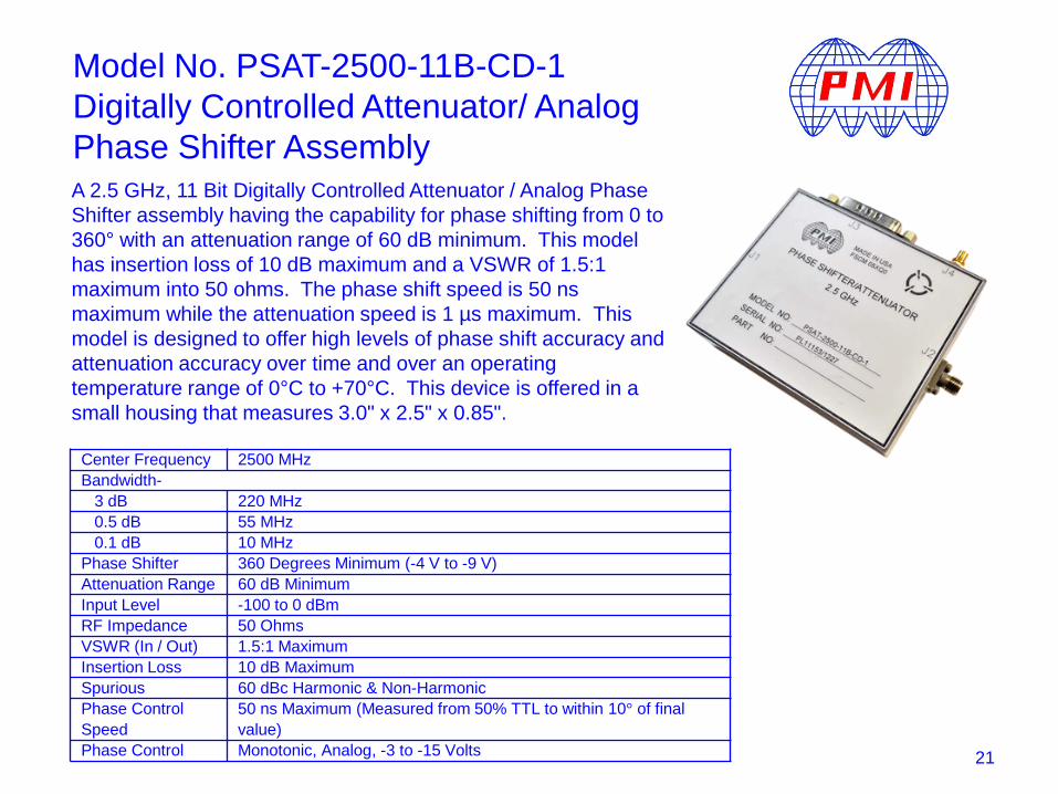
Model No. PSAT-2500-11B-CD-1 Digitally Controlled Attenuator/ Analog Phase Shifter AssemblyA 2.5 GHz, 11 Bit Digitally Controlled Attenuator / Analog Phase Shifter assembly having the capability for phase shifting from 0 to 360° with an attenuation range of 60 dB minimum. This model has insertion loss of 10 dB maximum and a VSWR of 1.5:1 maximum into 50 ohms. The phase shift speed is 50 ns maximum while the attenuation speed is 1 µs maximum. This model is designed to offer high levels of phase shift accuracy and attenuation accuracy over time and over an operating temperature range of 0°C to +70°C. This device is offered in a small housing that measures 3.0" x 2.5" x 0.85".
Center Frequency 2500 MHzBandwidth-
3 dB 220 MHz0.5 dB 55 MHz0.1 dB 10 MHz
Phase Shifter 360 Degrees Minimum (-4 V to -9 V)Attenuation Range 60 dB MinimumInput Level -100 to 0 dBmRF Impedance 50 OhmsVSWR (In / Out) 1.5:1 MaximumInsertion Loss 10 dB MaximumSpurious 60 dBc Harmonic & Non-HarmonicPhase Control Speed
50 ns Maximum (Measured from 50% TTL to within 10° of final value)
Phase Control Monotonic, Analog, -3 to -15 Volts

22
Repeatability Deviation from vendor vs. supply voltage characteristics shall be less than 2°
Max / Min Slope Ratio 4Minimum Voltage Change for 360° 5 Volts
Attenuation Control Speed 1 s Maximum (50% TTL to within 0.1dB final attenuation over the 0 to 45 dB range)
Attenuation Control Monotonic, 11-Bit Parallel TTLAttenuation Step Size 0.0625 dB (60 dB = 960 Digital)Attenuation Accuracy at Center Frequency ±0.5 dB to 30 dB, ±1.0 dB from 30 dB to 50 dB Relative Attenuation Accuracy up to 1 dB Accurate to within 0.1 dBPM / AM 0.8 dB peak-peak Maximum over 360°
AM / PM Peak-Peak phase shift at constant phase setting at center frequency (2500 MHz) shall be less than 4.0°, attenuation 0 to 40 dB
Phase vs. Frequency Variation over 0.88% Bandwidth (22 MHz) ±1°
Phase vs. Frequency Variation over 2.2% Bandwidth (55 MHz) ±3°Phase vs. Frequency Variation over 8.8% Bandwidth (220 MHz) ±7°
Deviation from Linear over 2.2% Bandwidth (55 MHz) ±1°Deviation from Linear over 8.8% Bandwidth (55 MHz) ±5°Absolute Attenuation Temperature Stability Variation at any setting < 1.25 dB with respect to the value at 25 °C
Relative Attenuation Temperature StabilityVariation between any two devices (Over all relative attenuation and phase settings) shall be less than 1.4 dB with respect to the value at 25°C and less than 0.5dB over any 20°C change
Absolute Phase Temperature Stability Variation at any setting < 8° with respect to the value at 25 °C
Relative Phase Temperature StabilityVariation between any two devices (Over all relative attenuation and phase settings) shall be less than 4° with respect to the value at 25 °C and less than 2° over any 20 °C change
LSB 0.03125 dB
Model No. PSAT-2500-11B-CD-1 Digitally Controlled Attenuator/ Analog Phase Shifter Assembly

23
Model No. PSAT-2500-11B-CD-1 Digitally Controlled Attenuator/ Analog Phase Shifter Assembly

24
Model No. PSL-13D414D2-CD-PP 13.4 to 14.2 GHz, Integrated High Power Switch Limiter
PSL-13D414D2-CD-PP is a switch limiter operating in the 13.4 to 14.2 GHz frequency range. A +10mA bias will turn the switch off while a -10 mA bias will turn the switch into the insertion loss state. The integrated limiter will handle 20 W having a 2 µs pulse width.
Frequency Range 13.4 to 14.2 GHz
Maximum Peak Power75 W for 300 ns Pulse Width (At Switch)20 W for 2 us Pulse Width (At Limiter)
Maximum Average Power 10 W (At Switch)1 W (At Limiter)
Leakage Power +20 dBm Max
Switching Bias Conditions +10 mA (High Loss)-10 mA (Low Loss)
Insertion Loss 1.3 dB Max
Return Loss (-10mA Condition) -15 dB Max
Rise Time (Input CW Power < 1dB Compression Point) 20 ns Max
Fall Time (Input CW Power < 1dB Compression Point) 20 ns Max
Blanking Isolation 40 dB Min
Recovery Time (RF Power High to Low Within 1dB) 100 ns Max
Sealing Hermetic

25
Typical Blanking Performance Plot
Typical Insertion Loss and VSWR Plot
Model No. PSL-13D414D2-CD-PP 13.4 to 14.2 GHz, Integrated High Power Switch Limiter
26
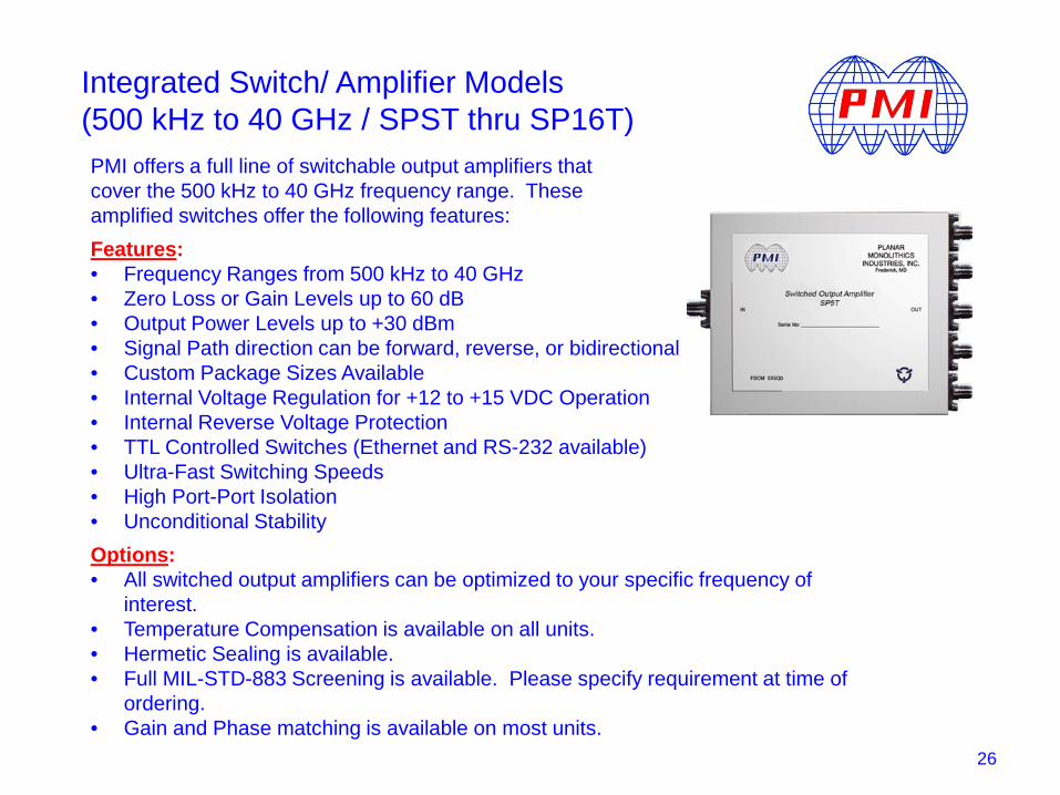
PMI offers a full line of switchable output amplifiers that cover the 500 kHz to 40 GHz frequency range. These amplified switches offer the following features:Features:• Frequency Ranges from 500 kHz to 40 GHz • Zero Loss or Gain Levels up to 60 dB • Output Power Levels up to +30 dBm • Signal Path direction can be forward, reverse, or bidirectional • Custom Package Sizes Available • Internal Voltage Regulation for +12 to +15 VDC Operation • Internal Reverse Voltage Protection• TTL Controlled Switches (Ethernet and RS-232 available)• Ultra-Fast Switching Speeds• High Port-Port Isolation• Unconditional Stability Options:• All switched output amplifiers can be optimized to your specific frequency of
interest.• Temperature Compensation is available on all units.• Hermetic Sealing is available.• Full MIL-STD-883 Screening is available. Please specify requirement at time of
ordering.• Gain and Phase matching is available on most units.
Integrated Switch/ Amplifier Models(500 kHz to 40 GHz / SPST thru SP16T)

Model No. PIA-BTFL-GPO-2CHIntegrated Bias-T, Band Pass Filter with Limited Output
PARAMETERS SPECIFICATIONS
PASSBAND LOWER LIMIT 2.0 GHz Typ
PASSBAND UPPER LIMITER 19.0 GHz Min
-3 dB Cut off 1.85 dB Typ
PASSBAND INSERTION LOSS 1.85 dB Typ, 2.5 dB Max
REJECTION -15 dBm Min @ 1.7 GHz-20 dBm Min @ DC to 1.5 GHz
PASSBAND VSWR 2.0:1 Max
BIAS Rise/Fall90% to 10% / 10% to 90% 50 ns Max
LIMITING THRESHOLD +8 dBm Min
PULSE RECOVERY TIME 50 ns Max(to within 1 dB of IL)
SµspendedSubstrateBandpass
Filter
Bias-T Limiter
27
Model No. PSD-2G6G-CD-1 & PSD-6G18G-CD-2High Power Switch/ Limiter Assembly
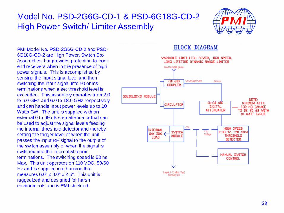
PMI Model No. PSD-2G6G-CD-2 and PSD-6G18G-CD-2 are High Power, Switch Box Assemblies that provides protection to front-end receivers when in the presence of high power signals. This is accomplished by sensing the input signal level and then switching the input signal into 50 ohms terminations when a set threshold level is exceeded. This assembly operates from 2.0 to 6.0 GHz and 6.0 to 18.0 GHz respectively and can handle input power levels up to 10 Watts CW. The unit is supplied with an external 0 to 69 dB step attenuator that can be used to adjust the signal levels feeding the internal threshold detector and thereby setting the trigger level of when the unit passes the input RF signal to the output of the switch assembly or when the signal is switched into the internal 50 ohms terminations. The switching speed is 50 ns Max. This unit operates on 110 VDC, 50/60 Hz and is supplied in a housing that measures 6.0” x 8.0” x 2.5”. This unit is ruggedized and designed for harsh environments and is EMI shielded.
28

Model No. PSD-2G6G-CD-22.0 to 6.0 GHz, High Power Switch/ Limiter Assembly
Final Assembly:Frequency Response 2.0 to 6.0 GHzPower 110 VAC Only, 50/60 GHzSize 6.0” X 8.0” X 2.5”Finish Painted GrayWeight 20 lbs Typ
Pin Diode Switch:Power Handling >= 10 WFrequency Response 2.0 to 6.0 GHzSwitching Speed < 50ns
Threshold Detector:Frequency Repsonse 2.0 to 6.0 GHzSwitching Speed < 50 nsOutput Type TTL (Compatible with Pin Switch)Sensitivity < -40 dBm
Max Power (No Damage) 10 dBm
Coupler:Power Handling >= 10 WFrequency Response 2.0 to 6.0 GHzCoupling Factor 20 dB
50 Ohm LOAD:Power Handling >= 10 WFrequency Response 2.0 to 6.0 GHz
Attenuator:Power Handling > 2 WFrequency Response 2.0 to 6.0 GHz
Attenuation 0 - 69 By (1) Front Panel Knob or Thumb Wheel
29

Model No. PSD-6G18G-CD-26.0 to 18.0 GHz, High Power Switch/ Limiter Assembly
Final Assembly:Frequency Response 6.0 to 18.0 GHzPower 110 VAC Only, 50/60 GHzSize 6.0” X 8.0” X 2.5”Finish Painted GrayWeight 20 lbs Typ
Pin Diode Switch:Power Handling ≥ 10 WFrequency Response 6.0 to 18.0 GHzSwitching Speed < 50 ns
Threshold Detector:Frequency Repsonse 6.0 to 18.0 GHzSwitching Speed < 50nsOutput Type TTL (Compatible with Pin Switch)Sensitivity < -40 dBm
Max Power (No Damage) 10 dBm
Coupler:Power Handling >= 10 WFrequency Response 6.0 to 18.0 GHzCoupling Factor 20 dB
50 Ohm LOAD:Power Handling >= 10 WFrequency Response 6.0 to 18.0 GHz
Attenuator:Power Handling > 2WFrequency Response 6.0 to 18.0 GHz
Attenuation 0 - 69 By (1) Front Panel Knob or Thumb Wheel
30
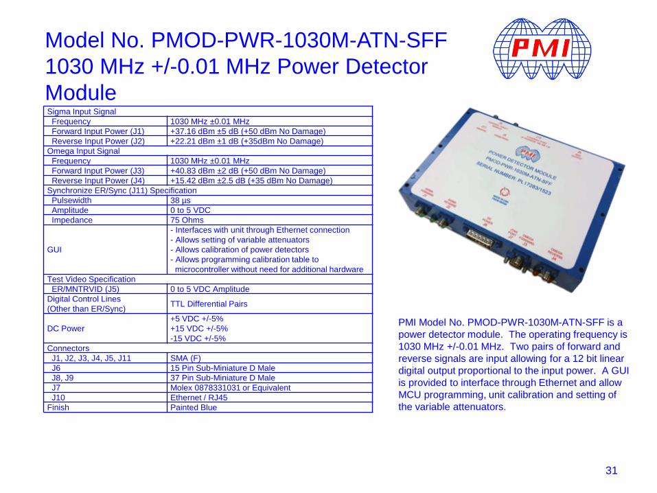
Model No. PMOD-PWR-1030M-ATN-SFF1030 MHz +/-0.01 MHz Power Detector Module
31
Sigma Input SignalFrequency 1030 MHz ±0.01 MHzForward Input Power (J1) +37.16 dBm ±5 dB (+50 dBm No Damage)Reverse Input Power (J2) +22.21 dBm ±1 dB (+35dBm No Damage)
Omega Input SignalFrequency 1030 MHz ±0.01 MHzForward Input Power (J3) +40.83 dBm ±2 dB (+50 dBm No Damage)Reverse Input Power (J4) +15.42 dBm ±2.5 dB (+35 dBm No Damage)
Synchronize ER/Sync (J11) SpecificationPulsewidth 38 µsAmplitude 0 to 5 VDCImpedance 75 Ohms
GUI
- Interfaces with unit through Ethernet connection- Allows setting of variable attenuators- Allows calibration of power detectors- Allows programming calibration table to
microcontroller without need for additional hardwareTest Video Specification
ER/MNTRVID (J5) 0 to 5 VDC AmplitudeDigital Control Lines(Other than ER/Sync) TTL Differential Pairs
DC Power+5 VDC +/-5%+15 VDC +/-5%-15 VDC +/-5%
ConnectorsJ1, J2, J3, J4, J5, J11 SMA (F)J6 15 Pin Sub-Miniature D MaleJ8, J9 37 Pin Sub-Miniature D MaleJ7 Molex 0878331031 or EquivalentJ10 Ethernet / RJ45
Finish Painted Blue
PMI Model No. PMOD-PWR-1030M-ATN-SFF is a power detector module. The operating frequency is 1030 MHz +/-0.01 MHz. Two pairs of forward and reverse signals are input allowing for a 12 bit linear digital output proportional to the input power. A GUI is provided to interface through Ethernet and allow MCU programming, unit calibration and setting of the variable attenuators.

32
FRONT
REAR
FUNCTIONAL BLOCK DIAGRAM
Model No. PMOD-PWR-1030M-ATN-SFF1030 MHz +/-0.01 MHz Power Detector Module

MARPS-30M6G-3U-1 is a Multiagent Radio Frequency Path Simulator consisting of an integrated amplified attenuator assembly and an 8-Way Amplified Power Divider that operate over the 30 MHz to 6.0 GHz frequency range in order to simulate field testing in a reduced, controlled lab environment.
33
Model No. MARPS-30M6G-3U-1Multiagent Radio Frequency Path Simulator
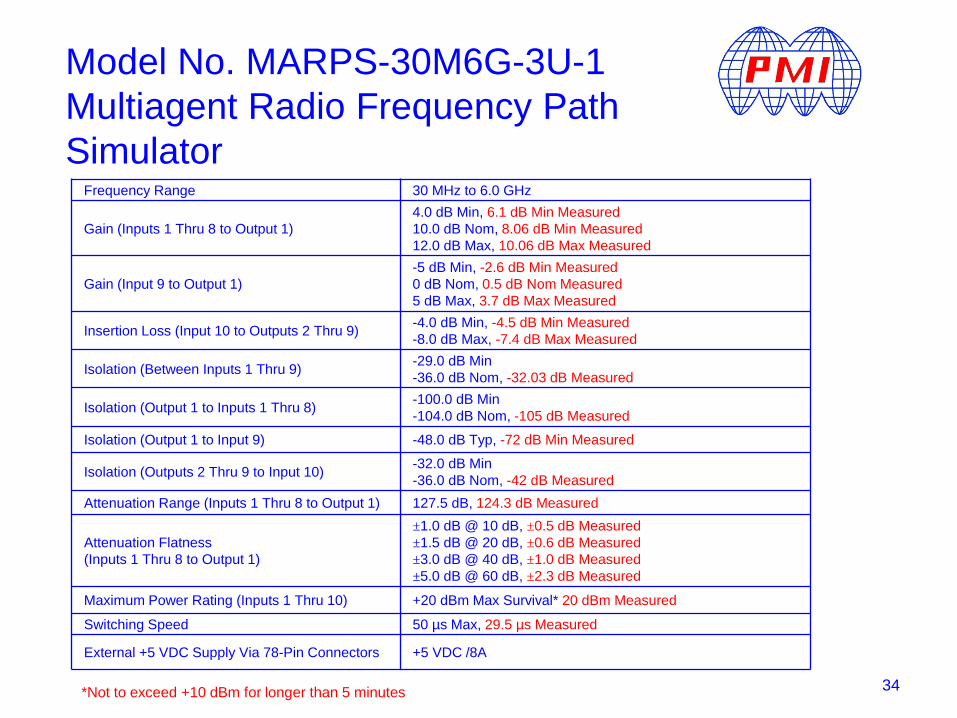
34*Not to exceed +10 dBm for longer than 5 minutes
Frequency Range 30 MHz to 6.0 GHz
Gain (Inputs 1 Thru 8 to Output 1)4.0 dB Min, 6.1 dB Min Measured10.0 dB Nom, 8.06 dB Min Measured12.0 dB Max, 10.06 dB Max Measured
Gain (Input 9 to Output 1)-5 dB Min, -2.6 dB Min Measured0 dB Nom, 0.5 dB Nom Measured5 dB Max, 3.7 dB Max Measured
Insertion Loss (Input 10 to Outputs 2 Thru 9) -4.0 dB Min, -4.5 dB Min Measured-8.0 dB Max, -7.4 dB Max Measured
Isolation (Between Inputs 1 Thru 9) -29.0 dB Min-36.0 dB Nom, -32.03 dB Measured
Isolation (Output 1 to Inputs 1 Thru 8) -100.0 dB Min-104.0 dB Nom, -105 dB Measured
Isolation (Output 1 to Input 9) -48.0 dB Typ, -72 dB Min Measured
Isolation (Outputs 2 Thru 9 to Input 10) -32.0 dB Min-36.0 dB Nom, -42 dB Measured
Attenuation Range (Inputs 1 Thru 8 to Output 1) 127.5 dB, 124.3 dB Measured
Attenuation Flatness (Inputs 1 Thru 8 to Output 1)
±1.0 dB @ 10 dB, ±0.5 dB Measured±1.5 dB @ 20 dB, ±0.6 dB Measured±3.0 dB @ 40 dB, ±1.0 dB Measured±5.0 dB @ 60 dB, ±2.3 dB Measured
Maximum Power Rating (Inputs 1 Thru 10) +20 dBm Max Survival* 20 dBm Measured
Switching Speed 50 µs Max, 29.5 µs Measured
External +5 VDC Supply Via 78-Pin Connectors +5 VDC /8A
Model No. MARPS-30M6G-3U-1Multiagent Radio Frequency Path Simulator

35
Model No. PMA-218-LSP2.0 to 18.0 GHz, Modulator Amplifier
This modulator amplifier capable of amplitude modulation, level control and pulse modulation for an RF stimulus path that works from 0.5 to 2.0 GHz and 2.0 to 18.0 GHz. This integrated module contains switches, modulators, attenuators and amplifiers and is built using MIC/MMIC technology.

36
Frequency Range (J2 to J3) 2.0 to 18.0 GHz(J1 to J3) 0.5 to 2.0 GHz
Power Output at 1.0 dB Compression(Fendamental) into a 1.5:1 maximumVSWR (any phase)
+13.0 dBm Min
Third Order Intercept Point(output) +23.0 dBm Min
RF Input Power +14.0 dBm Max
RF Output Power +6.0 ± 2.0 dBm with 5.0 dB attenuation in the leveling attenuator and with an RF Input of +12.0 dBm
Pulse Modulation Depth 60.0 dBc Min
RF Pulse Width Range 200 ns to 100 µs
RF Pulse Rise Time (10% to 90%) 10 ns Max
RF Pulse Fall Time (90% to 10%) 15 ns Max
RF Pulse Repetition Interval 1 µs to 6 ms
RF Pulse Distortion ±2.0 dB Max variation
Pulse/CW Differential 0.3 dB Max variation
Pulse Width Fidelity ±20 ns Max deviation (between square law detected RF output pulse 50% points and control input 50% points)
Level Modulator (Mod A) 0.0 to 60.0 dB Min
Level Modulator Accuracy
±0.5 dB (0.0 to 10.0 dB)±1.0 dB (10.1 to 20.0 dB)±1.5 dB (20.1 to 40.0 dB)±2.0 dB (40.1 to 60.0 dB)
Sensitivity 6 dB/volt
Amplitude Modulator Depth (Mod B) 0.0 to 60.0 dB Min
Amplitude Modulator Depth Accuracy
±0.5 dB (0.0 to 10.0 dB)±1.0 dB (10.1 to 20.0 dB)±1.5 dB (20.1 to 40.0 dB)±2.0 dB (40.1 to 60.0 dB)
Amplitude Modulation Rate 1.0 Hz to 2.0 kHz
Noise Figure TBD dB Max
Harmonics at P1dB -20.0 dBc Min
Spurious Outputs -60.0 dBc Min, Measure from 0.5 to 18.0 GHz
VSWR (RF Input) 1.8:1 Max (Ref to 50 Ohms)1.8:1 Max (Ref to 50 Ohms)
Bias Voltages/Currents +15 VDC-15 VDC
Model No. PMA-218-LSP2.0 to 18.0 GHz, Modulator Amplifier

37
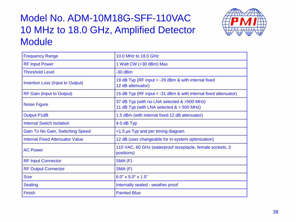
Model No. ADM-10M18G-SFF-110VAC10 MHz to 18.0 GHz, Amplified Detector Module
Model ADM-1018G-SFF-110VAC is a state-of-the-art 10 MHz to 18.0 GHz integrated subsystem that allows users to input RF signals and provide automatic detection when signal levels fall below -30 dBm and automatically switch in a low noise amplifier such that low level signals can remain detectable. The purpose of this module is to provide optimum RF signal levels to a RF/fiber converter module. The unit is powered by standard 100 VAC.The RF input / output are via a SMA female connector is configured such that the end user can change the value of the fixed attenuator level by changing the internal SMA screw-on attenuator such that in system optimization can be done.
38
Frequency Range 10.0 MHz to 18.0 GHz
RF Input Power 1 Watt CW (+30 dBm) Max
Threshold Level -30 dBm
Insertion Loss (Input to Output) 19 dB Typ (RF input > -29 dBm & with internal fixed 12 dB attenuator)
RF Gain (Input to Output) 15 dB Typ (RF input < -31 dBm & with internal fixed attenuator)
Noise Figure 37 dB Typ (with no LNA selected & >500 MHz)11 dB Typ (with LNA selected & > 500 MHz)
Output P1dB 1.5 dBm (with internal fixed 12 dB attenuator)
Internal Switch Isolation 4 0 dB Typ
Gain To No Gain, Switching Speed <1.5 µs Typ and per timing diagram
Internal Fixed Attenuator Value 12 dB (user changeable for in-system optimization)
AC Power 110 VAC, 60 GHz (waterproof receptacle, female sockets, 3 positions)
RF Input Connector SMA (F)
RF Output Connector SMA (F)
Size 6.0" x 5.0" x 1.5"
Sealing Internally sealed - weather proof
Finish Painted Blue
Model No. ADM-10M18G-SFF-110VAC10 MHz to 18.0 GHz, Amplified Detector Module

39
INSERTION LOSS PATH GAIN PATH
Model No. ADM-10M18G-SFF-110VAC10 MHz to 18.0 GHz, Amplified Detector Module

40
NOISE FIGURE (500 MHz – 18 GHz)GAIN PATH
NOISE FIGURE (100 MHz – 500 MHz)GAIN PATH
Model No. ADM-10M18G-SFF-110VAC10 MHz to 18.0 GHz, Amplified Detector Module

41
Model No. LCM-7R7G8R2G-CD-17.7 to 8.2 GHz, Amplified RF Laser Control Module
PMI Model No. LCM-7R7G8R2G-CD-1 is anAmplified RF Laser Control Module for useat a frequency of 7.7 to 8.2 GHz with an IFrange of DC to 10 KHz. It features a 20 dBvoltage programmable attenuator and a360° phase shifter. This model is designedfor low spectral noise and high reverseisolation, offered in a slim line housingmeasuring only 2.5" x 1.75" x 0.4".
Frequency Range 7.7 to 8.2 GHz
Gain J1 to J2 16 dB, ±2 dB max (Attenuation = 0 dB)
J2 Output 1dB Compression 28 dBm Typ
Conversion Gain 0 dB, ±3 dB Max (J1 = 10 dBm, J4 = -10 dBm)
Tap Out Insertion Loss 16 dB, ±2 dB Typ (J1 to J5)
Input Power J1 20 dBm Max
Input Power J4 14 dB Max
VSWR J1, J2, J3, J4, J5 2.2:1 Max
Power Supply +15 V @ +1000 mA Max-15 V @ -200 mA Max
Size 2.5" x 1.75" x 0.4"
Finish Gold Plated
Low Noise Amplifier 1, 2, 3
Gain 14 dB Typ
Saturated Output Power 16 dBm Typ
Noise Figure 2.5 dB Typ
Reverse Isolation 40 dB Typ
Phase Shifter
Phase Shift Range 0° to 360° Min
Control Range 0 to 10 Volts
Non-Linear Slope Ratio 4:1 Typ
Switching Speed 200 ns Max
Attenuator
Attenuation Range 0 to 20 dB Min
Control Range 0 to 10 Volts
Non-Linear Slope Ratio 8:1 Typ
Switching Speed 1.0 µs Max
Filter 1, 2, 3, 4, 5
Pass Band 7.7 to 8.2 GHz, (2 dB) Typ
Stop Band, Lower DC to 6.8 GHz (20 dB) Typ
Stop Band, Upper 10.3 to 18.0 GHz, (20 dB) Typ
Low Pass Active Filter
Pass Band DC to 10 KHz Min
Stop Band 10 KHz (Roll Off 6 dB per Octave) Typ

42
Model No. LCM-7R7G8R2G-CD-17.7 to 8.2 GHz, Amplified RF Laser Control Module

43
Gain J1 to J2 & VSWR
J4 (PTD) Input VSWR
Model No. LCM-7R7G8R2G-CD-17.7 to 8.2 GHz, Amplified RF Laser Control Module

44
PMI Model No. LCM-16G100MBW-CD-1 is an Amplified RF Laser Control Module for use at a frequency of 16.0 GHz, ±50 MHz with an IF range of DC to 10 kHz. It features a 20 dB voltage programmable attenuator and a 360° phase shifter. This model is designed for low spectral noise and high reverse isolation in a slimline housing.
Frequency Range 16.0 GHz ± 50 MHz
Gain J1 to J2 16 dB ± 2 dB Max (Attenuation = 0 dB)
J2 Output 1 dB Compression 26 dBm Typ
Conversion Gain 0 dB ± 3 dB Max(J1 = 10 dBm, J4 = -10 dBm)
Tap Out Insertion Loss 16 dB ± 2 dB Typ (J1 to J5)
Input Power J1 18 dBm Max
Input Power J4 14 dB Max
VSWR J1, J2, J3, J4, J5 2.2:1 Max
Power Supply+15 V @ 400 mA Max-15 V @ 200 mA Max +5 V @ 800 mA Max
Size 2.5" x 1.75" x 0.4"
Finish Gold Plated
Low Noise Amplifier 1, 2, 3
Gain 12 dB Typ
Saturated Output Power 15 dBm Typ
Noise Figure 2.5 dB Typ
Reverse Isolation 32 dB Typ
Phase Shifter
Phase Shift Range 0° to 360° Min
Control Range 0 to 10 Volts
Non-Linear Slope Ratio 4:1 Typ
Switching Speed 200 ns Max
Attenuator
Attenuation Range 0 to 20 dB Min
Control Range 0 to 10 Volts
Non-Linear Slope Ratio 8:1 Typ
Switching Speed 1.0 µs Max
Filter 1, 2, 3, 4, 5
Pass Band 16 GHz ± 50 MHz (2 dB) Typ
Stop Band, Lower DC to 12.0 GHz (20 dB) Typ
Stop Band, Upper 22.0 to 40.0 GHz (20 dB) Typ
Low Pass Active Filter
Pass Band DC to 10 kHz Min
Stop Band 10 kHz (Roll Off 6 dB per Octave) Typ
Model No. LCM-7R7G8R2G-CD-17.7 to 8.2 GHz, Amplified RF Laser Control Module

45
Model No. LCM-7R7G8R2G-CD-17.7 to 8.2 GHz, Amplified RF Laser Control Module

46
Model No. PL-MCU-ENET-TTL-14-10B-1UEthernet Microcontroller Test Box
PMI Model No. PL-MCU-ENET-TTL-14-10B-1U is an Ethernet Microcontroller Test Box which allows for an ethernet command to be sent up to 140 parallel TTL output bits. Fourteen 15-Pin D-Subminiature connectors are provided to control fourteen 10-Bit devices. +15 VDC is also provided on each connector to provide up to 50 Watts total to the external devices. A custom GUI is provided along with operating instructions with commands to allow the user to write their own GUI for direct control.
Size 10.06" x 17.06" x 1.73" (1U Chassis to fit in a 19" Rack)
Connectors AC ReceptacleD-15 Female(x14)
Output Connector
D-15 FemalePin 1 - TTL6Pin 2 - TTL5Pin 3 - TTL4Pin 4 - TTL3Pin 5 - GNDPin 6 - TTL2Pin 7 - TTL1Pin 8 - GNDPin 9 - NCPin 10 - NCPin 11 - +15VDCPin 12 - TTL10Pin 13 - TTL9Pin 14 - TTL8Pin 15 - TTL7
Ethernet Connector RJ-45Power Supply 100-120 VAC/60HzIP Address Factory PresetFinish Powder Coated Blue with Silkscreen

47
Model No. PL-MCU-ENET-TTL-14-10B-1UEthernet Microcontroller Test Box

48
Model No. PL-MCU-ENET-TTL-MAHEthernet Microcontroller Test Box
PMI Model No. PL-MCU-ENET-TTL-MAH is an Ethernet Microcontroller Test Box which allows for an ethernet command to be sent up to 18 parallel TTL output bits. This controller can be used with may PMI products that required parallel digital commands, such as switches, attenuators, phase shifters and IQ Modulators.
Size 4.5" x 3.0" x 1.5"
DC Power Connector D-9 Male
Output Connector
D-25 FemalePin 1 - TTL1 (MSB)Pin 2 - TTL2Pin 3 - TTL3Pin 4 - TTL4Pin 5 - TTL5Pin 6 - TTL6Pin 7 - TTL7Pin 8 - TTL8Pin 9 - TTL9Pin 10 - TTL10Pin 11 - TTL11Pin 12 - TTL12Pin 13 - TTL13Pin 14 - TTL14Pin 15 - TTL15Pin 16 - TTL16Pin 17 - TTL17Pin 18 - TTL18 (LSB)Pin 19 - GroundPin 20 thru 25 - No connection
Ethernet Connector RJ-45
Power Supply +5 V @ 150 mA Typ
IP Address Factory Preset
Finish Painted Blue

49
Model No. PL-MCU-ENET-TTL-MAHEthernet Microcontroller Test Box
50
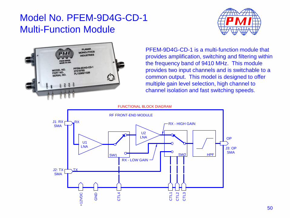
Model No. PFEM-9D4G-CD-1Multi-Function Module
PFEM-9D4G-CD-1 is a multi-function module that provides amplification, switching and filtering within the frequency band of 9410 MHz. This module provides two input channels and is switchable to a common output. This model is designed to offer multiple gain level selection, high channel to channel isolation and fast switching speeds.
FUNCTIONAL BLOCK DIAGRAM
U1LNA
U2LNA
SW1 SW2
RX
TX
OP
J3: OPSMA
J2: TXSMA
J1: RXSMA
+12V
DC
GN
D
CTL
4
CTL
2
RF FRONT-END MODULE
CTL
1
CTL
3
HPFRX - LOW GAIN
RX - HIGH GAIN

51
TX (State 1) RX Low Gain (State 2) RX High Gain (State 3)
Max Input Power at J1 0 dBm 14 dBm 14 dBm
Frequency 9410 MHz +/- 30 MHz 9410 MHz +/- 30 MHz 9410 MHz +/- 30 MHz
Gain 0 to -5 dBm 11 to 15 dBm 30 to 35 dBm
Gain Flatness <0.1 dBm <0.1 dBm <0.1 dBm
Noise Figure N/A 2 dB Nominal, 2.5 dB Max- Measured 2.2 dB
2dB Nominal, 2.5 dB Max- Measured 2.2 dB
VSWR 1.5:1 Typ 1.5:1 Typ 1.5:1 Typ
OP3 (Output) > 18 dBm Measured 18.7 dB
>18 dBm Measured 18.7 dB
>18 dBm Measured 18.7 dB
OP2 (Output) >8 dBm Measured 24.7 dB
>8 dBmMeasured 24.7 dB
>8 dBmMeasured 24.7 dB
Port to Port J1-J3 Isolation >85 dBMeasured 114 dB N/A N/A
Max Output Power +23 dBm - Measured 15.7 dBm
Output Signal Distortion No apparent droop or distortion with a pulse width of 500 to 1000 ns, at 500 to 2000 PPS
Video Switching Transients < -120 dBm above 1.7 GHz
Stability Unconditionally stable when terminated at J1, J2 and J3 with short circuit at all phases
Max Out-Of-Band Gain Below In-Band Gain for f > 6.5 GHz-20 dB Below In-Band Gain < 6.5 GHz
Switching Time 50 ns: TX to RX - Measured 28.4 ns50 ns: RX Low Gain to RX High Gain - Measured 36.4 ns
Switching Control 3.3 V to 5 V, TTL Compatible
BIAS V/I +12 VDC / 125 mA Typ - Measured 125 mA
Size 2.89' x 1.62" x 0.63
Finish Painted Gray
Model No. PFEM-9D4G-CD-1Multi-Function Module

52
Model No. PMOD-IFCPL-60M-AMP-3UIF Coupler Module
PMI Model No. PMOD-IFCPL-60M-AMP-3U is an IF Coupler Module on a 3U Open VPX card. The operating frequency is 60MHz. A test signal and 3 RF signals are input allowing for 3 output signals.

53
A1 Input Signal
IF Frequency 60 MHz
Maximum Input Power -11 dBm
Maximum VSWR 1.5:1 at IF - Measured 1.25:1
B1 Input Signal
IF Frequency 60 MHz
Maximum Input Power -11 dBm
Maximum VSWR 1.5:1 at IF - Measured 1.28:1
Ω Output Signal
IF Frequency 60 MHz
Maximum Input Power -8 dBm
Maximum VSWR 1;5:1 at IF - Measured 1.28:1
IF Input Signal
IF Frequency 60 MHz
Input Power Range -4 dBm to +5 dBm
Maximum VSWR 1.5:1 at IF - Measured 1.19:1
A1, B1 and Ω Output Signals
Absolute Maximum Output +10 dBm - Measured +8.32 dBm
Full Scale Output +3 dBm to +8 dBm - Measured +7.75 dBm
Differential Amplitude Change All three output gains within ±0.5 dB at IF -Measured ±0.33 dB
Differential Phase Change±3° for all frequencies within ±3 MHz of IF over the 14 MHz range centered at IF -Measured ±2.28°
Bandpass Filters (Frequency Response)
IF Frequency 60 MHz
3 dB Bandwidth ±8 MHz Centered on IF
Cutoff-40 dBc ±30 MHz Centered on IFNo Ripple above -40 dBc –Measured -40.8 dBc
Phase Response Linear within ±10° over 14 MHzRange Centered on IF - Measured ±2.58°
Differential Amplitude All three filters within ±0.5 dB at IF
Differential PhaseChannel A and B Filters to within ±3°over the 14 MHz range centered at IF -Measured ±2.28°
Bandpass Filters (Pulse Response)
Rise Time 160 ns max from 40 dB below Peak to 3 dB above Peak - Measured 36 ns
Fall Time 160 ns max from 3 dB below Peak to 40 dB - Measured 40 ns
Amplifying Limiters
Absolute Maximum Output +10 dBm
Full Scale Output +8 dBm
Connectors/ Finish
SMA Female IF Input, A1 Input, B1 Input, Ω Input
SSMC Female A1 Output, B1 Output, Ω Output
9-Pin Sub-Miniature D Female Power
Finish Painted Blue
Model No. PMOD-IFCPL-60M-AMP-3UIF Coupler Module

54
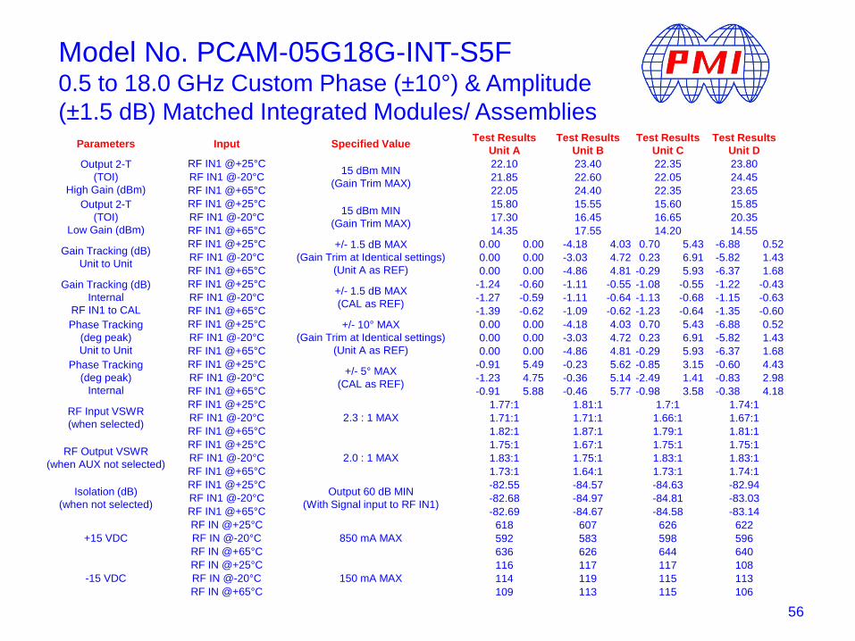
Model No. PCAM-05G18G-INT-S5F0.5 to 18.0 GHz Custom Phase (±10°) & Amplitude (±1.5 dB) Matched Integrated Modules/ AssembliesThese integrated modules are built in sets of four, and are phase and amplitude matched to industry leading levels of ±10° and ±1.5 dB over the 0.5 to 18.0 GHz frequency range. Incorporating limiters, LNAs, switches, and variable digital attenuators, these units allow for high and low gain paths, a calibration input and auxiliary channel. A low noise figure and high output of +15 dBm OP1dB are achieved by utilizing system analysis software and in-house hybrid/MIC processes. These hermetically sealed units are built do withstand the most stringent military airborne environments.

55
Model No. PCAM-05G18G-INT-S5F0.5 to 18.0 GHz Custom Phase (±10°) & Amplitude (±1.5 dB) Matched Integrated Modules/ Assemblies
Parameters Input Specified Value Test Results Unit A
Test Results Unit B
Test Results Unit C
Test Results Unit D
Frequency Range RF IN1 0.5 GHz to 6 GHz
High Gain Path(dB)RF IN1 @+25°C
29 dB MIN, 33 dB MAX (Gain Trim MIN)
26.03 29.06 25.72 29.29 26.12 28.55 26.01 29.20RF IN1 @-20°C 27.09 29.63 27.06 29.50 26.96 29.24 27.27 29.62RF IN1 @+65°C 24.78 28.37 24.35 28.70 24.73 27.98 24.79 28.81
Low Gain Path(dB)RF IN1 @+25°C 13 dB MIN, 17 dB MAX
(Gain Trim MIN)11.54 14.92 10.69 14.00 11.01 13.76 10.86 13.99
RF IN1 @-20°C 12.48 15.03 11.68 14.28 11.75 14.11 11.97 14.35RF IN1 @+65°C 10.38 14.01 9.27 13.44 9.74 12.96 9.69 13.50
Gain Flatness(±dB)RF IN1 @+25°C ±1 dB Max over any
500 MHz BandHigh/Low
0.42 0.45 0.37 0.38RF IN1 @-20°C 0.47 0.47 0.51 0.47RF IN1 @+65°C 0.48 0.59 0.44 0.49
Noise FigureHigh Gain(dB)
RF IN1 @+25°C0.5 GHz to 2 GHz 6 dB MAX, 5 dB TYP (Gain Trim MAX)
5.12 5.09 5.16 5.07RF IN1 @-20°C 5.60 5.56 5.87 4.92RF IN1 @+65°C 6.37 5.49 6.53 6.25RF IN1 @+25°C
2 GHz to 6 GHz 5.5 dB MAX, 4.5 dB TYP (Gain Trim MAX)
4.69 4.93 4.87 4.82RF IN1 @-20°C 4.69 4.71 4.96 4.30RF IN1 @+65°C 5.77 5.46 6.01 5.91
Noise FigureLow Gain(dB)
RF IN1 @+25°C0.5 GHz to 6 GHz 16 dB MAX, (Gain
Trim MAX)
14.15 14.92 15.13 14.82RF IN1 @-20°C 15.98 16.83 17.37 14.70RF IN1 @+65°C 17.22 15.69 18.30 17.68
Compression Point(P-1dB)
High Gain (dBm)
RF IN1 @+25°C6 dBm MIN
(Gain Trim MAX)
14.71 17.21 14.33 14.55RF IN1 @-20°C 14.90 17.61 13.55 16.74RF IN1 @+65°C 14.20 13.10 13.71 14.14
Compression Point(P-1dB)
Low Gain (dBm)
RF IN1 @+25°C6 dBm MIN
(Gain Trim MAX)
5.31 8.22 4.96 5.18RF IN1 @-20°C 6.45 8.96 4.55 9.71RF IN1 @+65°C 3.82 2.79 3.35 3.52
56
Model No. PCAM-05G18G-INT-S5F0.5 to 18.0 GHz Custom Phase (±10°) & Amplitude (±1.5 dB) Matched Integrated Modules/ Assemblies
Parameters Input Specified Value Test Results Unit A
Test Results Unit B
Test Results Unit C
Test Results Unit D
Output 2-T(TOI)
High Gain (dBm)
RF IN1 @+25°C 15 dBm MIN (Gain Trim MAX)
22.10 23.40 22.35 23.80RF IN1 @-20°C 21.85 22.60 22.05 24.45RF IN1 @+65°C 22.05 24.40 22.35 23.65
Output 2-T(TOI)
Low Gain (dBm)
RF IN1 @+25°C 15 dBm MIN (Gain Trim MAX)
15.80 15.55 15.60 15.85RF IN1 @-20°C 17.30 16.45 16.65 20.35RF IN1 @+65°C 14.35 17.55 14.20 14.55
Gain Tracking (dB)Unit to Unit
RF IN1 @+25°C +/- 1.5 dB MAX (Gain Trim at Identical settings)
(Unit A as REF)
0.00 0.00 -4.18 4.03 0.70 5.43 -6.88 0.52RF IN1 @-20°C 0.00 0.00 -3.03 4.72 0.23 6.91 -5.82 1.43RF IN1 @+65°C 0.00 0.00 -4.86 4.81 -0.29 5.93 -6.37 1.68
Gain Tracking (dB)Internal
RF IN1 to CAL
RF IN1 @+25°C +/- 1.5 dB MAX (CAL as REF)
-1.24 -0.60 -1.11 -0.55 -1.08 -0.55 -1.22 -0.43RF IN1 @-20°C -1.27 -0.59 -1.11 -0.64 -1.13 -0.68 -1.15 -0.63RF IN1 @+65°C -1.39 -0.62 -1.09 -0.62 -1.23 -0.64 -1.35 -0.60
Phase Tracking (deg peak)Unit to Unit
RF IN1 @+25°C +/- 10° MAX (Gain Trim at Identical settings)
(Unit A as REF)
0.00 0.00 -4.18 4.03 0.70 5.43 -6.88 0.52RF IN1 @-20°C 0.00 0.00 -3.03 4.72 0.23 6.91 -5.82 1.43RF IN1 @+65°C 0.00 0.00 -4.86 4.81 -0.29 5.93 -6.37 1.68
Phase Tracking (deg peak)
Internal
RF IN1 @+25°C +/- 5° MAX (CAL as REF)
-0.91 5.49 -0.23 5.62 -0.85 3.15 -0.60 4.43RF IN1 @-20°C -1.23 4.75 -0.36 5.14 -2.49 1.41 -0.83 2.98RF IN1 @+65°C -0.91 5.88 -0.46 5.77 -0.98 3.58 -0.38 4.18
RF Input VSWR (when selected)
RF IN1 @+25°C2.3 : 1 MAX
1.77:1 1.81:1 1.7:1 1.74:1RF IN1 @-20°C 1.71:1 1.71:1 1.66:1 1.67:1RF IN1 @+65°C 1.82:1 1.87:1 1.79:1 1.81:1
RF Output VSWR (when AUX not selected)
RF IN1 @+25°C2.0 : 1 MAX
1.75:1 1.67:1 1.75:1 1.75:1RF IN1 @-20°C 1.83:1 1.75:1 1.83:1 1.83:1RF IN1 @+65°C 1.73:1 1.64:1 1.73:1 1.74:1
Isolation (dB)(when not selected)
RF IN1 @+25°C Output 60 dB MIN(With Signal input to RF IN1)
-82.55 -84.57 -84.63 -82.94RF IN1 @-20°C -82.68 -84.97 -84.81 -83.03RF IN1 @+65°C -82.69 -84.67 -84.58 -83.14
+15 VDCRF IN @+25°C
850 mA MAX618 607 626 622
RF IN @-20°C 592 583 598 596RF IN @+65°C 636 626 644 640
-15 VDCRF IN @+25°C
150 mA MAX116 117 117 108
RF IN @-20°C 114 119 115 113RF IN @+65°C 109 113 115 106

57
Model No. PCAM-05G18G-INT-S5F0.5 to 18.0 GHz Custom Phase (±10°) & Amplitude (±1.5 dB) Matched Integrated Modules/ Assemblies
Parameters Input Specified Value Test Results Unit A
Test Results Unit B
Test Results Unit C
Test Results Unit D
Frequency Range RF IN2 6 GHz to 18 GHz
High Gain Path(dB)
RF IN2 @+25°C
29 dB MIN, 33 dB MAX (Gain Trim MIN)
29.93 31.95 28.82 30.39 28.88 31.4629.1
7 31.04
RF IN2 @-20°C 31.51 33.78 30.70 33.04 30.48 33.1230.9
2 33.49
RF IN2 @+65°C 27.42 29.96 26.58 28.51 26.92 29.9227.2
6 28.72
Low Gain Path(dB)
RF IN2 @+25°C
13 dB MIN, 17 dB MAX (Gain Trim MIN)
12.65 16.92 13.59 15.59 12.47 16.8113.4
0 15.86
RF IN2 @-20°C 14.73 18.63 16.02 17.93 14.85 18.7815.4
7 18.23
RF IN2 @+65°C 9.74 14.94 10.79 14.06 9.76 15.4111.4
4 13.86
Gain Flatness(±dB)RF IN2 @+25°C ±1 dB Max over any
500 MHz Band
0.66 0.41 0.67 0.38RF IN2 @-20°C 0.62 0.41 0.65 0.51RF IN2 @+65°C 0.51 0.47 0.64 0.36
Noise FigureHigh Gain(dB)
RF IN2 @+25°C 6 GHz to 15 GHz 5.5 dB MAX, 4.5 dB TYP (Gain Trim MAX)
4.12 4.38 4.69 4.90RF IN2 @-20°C 3.80 3.86 4.30 4.36RF IN2 @+65°C 5.00 5.03 5.36 5.86RF IN2 @+25°C 15 GHz to 18 GHz 6 dB MAX,
5 dB TYP (Gain Trim MAX)
4.77 4.63 5.11 6.94RF IN2 @-20°C 4.41 4.16 4.62 5.24RF IN2 @+65°C 5.78 5.33 5.99 6.90
Noise FigureLow Gain(dB)
RF IN2 @+25°C 6 GHz to 18 GHz 16 dB MAX, (Gain Trim MAX)
14.57 12.99 15.77 15.40RF IN2 @-20°C 13.99 11.63 14.30 13.89RF IN2 @+65°C 17.60 14.73 17.67 18.21
Compression Point(P-1dB)
High Gain (dBm)
RF IN2 @+25°C 6 dBm MIN(Gain Trim MAX)
12.77 13.14 13.39 14.45RF IN2 @-20°C 13.01 13.49 13.46 15.16RF IN2 @+65°C 11.77 11.75 12.09 13.51
Compression Point(P-1dB)
Low Gain (dBm)
RF IN2 @+25°C 6 dBm MIN (Gain Trim MAX)
5.26 8.16 10.02 4.65RF IN2 @-20°C 6.46 9.61 7.95 8.99RF IN2 @+65°C 3.28 3.39 3.68 3.88

58
Model No. PCAM-05G18G-INT-S5F0.5 to 18.0 GHz Custom Phase (±10°) & Amplitude (±1.5 dB) Matched Integrated Modules/ Assemblies
Parameters Input Specified Value Test Results Unit A
Test Results Unit B
Test Results Unit C
Test Results Unit D
Output 2-T(TOI)
High Gain (dBm)
RF IN2 @+25°C 15 dBm MIN (Gain Trim MAX)
19.35 20.25 19.90 19.85RF IN2 @-20°C 20.35 20.55 20.35 21.20RF IN2 @+65°C 17.75 18.40 19.15 17.85
Output 2-T(TOI)
Low Gain (dBm)
RF IN2 @+25°C 15 dBm MIN (Gain Trim MAX)
11.90 15.90 15.10 13.55RF IN2 @-20°C 12.60 14.55 15.05 17.40RF IN2 @+65°C 10.35 13.05 12.10 12.70
Gain Tracking (dB)Unit to Unit
RF IN2 @+25°C +/- 1.5 dB MAX (Gain Trim at Identical settings)
(Unit A as REF)
0.00 0.00 -2.19 -0.01 -1.98 0.21 -2.00 0.45RF IN2 @-20°C 0.00 0.00 -2.04 0.17 -2.01 0.29 -2.17 0.93RF IN2 @+65°C 0.00 0.00 -2.25 -0.12 -2.02 0.19 -1.82 0.39
Gain Tracking (dB)Internal
RF IN2 to CAL
RF IN2 @+25°C+/- 1.5 dB MAX (CAL as REF)
-1.65 -0.36 -2.05 -0.35 -2.07 -0.45 -2.71 -0.33RF IN2 @-20°C -1.56 -0.32 -2.05 -0.37 -2.08 -0.47 -2.66 -0.18RF IN2 @+65°C -1.75 -0.35 -2.07 -0.53 -2.11 -0.53 -2.80 -0.28
Phase Tracking (deg peak)Unit to Unit
RF IN2 @+25°C +/- 10° MAX (Gain Trim at Identical settings)
(Unit A as REF)
0.00 0.00 -23.96 0.50 -1.55 28.70 -15.24 1.07RF IN2 @-20°C 0.00 0.00 -24.53 1.37 -1.09 30.88 -12.03 3.27RF IN2 @+65°C 0.00 0.00 -24.12 -0.96 -1.37 29.05 -15.63 1.34
Phase Tracking (deg peak)
Internal
RF IN2 @+25°C+/- 5° MAX
(CAL as REF)
-0.07 11.88 -0.92 11.65 -3.52 8.14 -4.09 9.72RF IN2 @-20°C -0.21 10.59 -2.25 10.78 -5.94 5.19 -6.09 7.21RF IN2 @+65°C 0.04 12.51 -0.44 12.20 -2.86 9.45 -3.52 12.17
RF Input VSWR (when selected)
RF IN2 @+25°C2.3 : 1 MAX
2.24:1 2.19:1 2.28:1 2.36:1RF IN2 @-20°C 2.34:1 2.4:1 2.34:1 2.48:1RF IN2 @+65°C 2.28:1 2.2:1 2.3:1 2.35:1
RF Output VSWR (when AUX not
selected)
RF IN2 @+25°C2.0 : 1 MAX
1.9:1 1.87:1 1.96:1 1.98:1RF IN2 @-20°C 1.94:1 1.95:1 2.02:1 2.07:1RF IN2 @+65°C 1.87:1 1.89:1 1.96:1 1.94:1
Isolation (dB)(when not selected)
RF IN2 @+25°C Output 60 dB MIN(With Signal input to RF IN2)
-60.44 -63.01 -66.16 -64.66RF IN2 @-20°C -60.75 -64.29 -67.64 -65.71RF IN2 @+65°C -59.75 -62.71 -63.83 -64.12
AUX Input VSWR (when selected)
AUX IN @+25°C2.3 : 1 MAX
1.84:1 1.71:1 1.82:1 1.6:1AUX IN @-20°C 1.83:1 1.77:1 1.97:1 1.62:1AUX IN @+65°C 1.83:1 1.69:1 1.77:1 1.6:1

59
Model No. PCAM-05G18G-INT-S5F0.5 to 18.0 GHz Custom Phase (±10°) & Amplitude (±1.5 dB) Matched Integrated Modules/ Assemblies
Parameters Input Specified Value Test Results Unit A
Test Results Unit B
Test Results Unit C
Test Results Unit D
AUX Input VSWR (when not selected)
AUX IN @+25°C2.0 : 1 MAX
1.61:1 1.59:1 1.5:1 1.52:1AUX IN @-20°C 1.66:1 1.64:1 1.99:1 1.6:1AUX IN @+65°C 1.55:1 1.53:1 1.77:1 1.46:1
Aux Insertion Loss(dB)
(when selected)
RF OUT @+25°C 7 dB MAX(Gain Trim MIN)
-7.30 -7.73 -7.76 -7.48RF OUT @-20°C -7.24 -7.65 -7.67 -7.41RF OUT @+65°C -7.64 -8.07 -8.11 -7.83
Isolation (dB)(when not selected)
AUX IN @+25°C Output 60 dB MIN(With Signal input to AUX IN)
-62.67 -60.02 -60.57 -59.53AUX IN @-20°C -62.30 -58.99 -58.83 -60.06AUX IN @+65°C -62.53 -60.13 -61.29 -59.69
CAL Input VSWR (0.5 to 6 GHz)
CAL @+25°C2.3 : 1 MAX
1.5:1 2.11:1 1.63:1 1.59:1CAL @-20°C 1.49:1 2.04:1 1.69:1 1.58:1CAL @+65°C 1.54:1 2.16:1 1.68:1 1.65:1
CAL Input VSWR (6 to 18 GHz)
CAL @+25°C2.3 : 1 MAX
2.24:1 2.28:1 2.15:1 2.35:1CAL @-20°C 2.28:1 2.36:1 2.29:1 2.35:1CAL @+65°C 2.23:1 2.26:1 2.16:1 2.28:1

2 - FORM, FIT & FUNCTION PRODUCTS
60

FORM, FIT & FUNCTION PRODUCTSIf you can not find the required components due to parts obsolescence please contact µs. We offer form, fit, and function replacement parts for any system. If a Source Control Drawing (SCD) is available we can offer a complete solution to meet all of the given electrical, mechanical and environmental specifications.
Specializing in aftermarket technology manufacturing and support for discontinued RF components, electronic circuits, digital circuits and Integrated circuits, PMI has the technical expertise to manufacture, supply and support these requirements. We are dedicated to assuring our cµstomer base that older discontinued products will continue to be available.
• IF & RF LOG AMPLIFIERS• VARIABLE GAIN AMPLIFIERS• SUCCESSIVE DETECTION LOG VIDEO AMPLIFIERS (SDLVA’s)• BI-PHASE MODULATORS• PHASE SHIFTERS• I & Q VECTOR MODULATORS• FREQUENCY DISCRIMINATORS• FILTERS• DIPLEXERS & MULTIPLEXERS• SWITCH FILTER BANKS• SUPERCOMPONENTS, SUBSYSTEMS AND SYSTEMS• SMT VOLTAGE REGULATORS• DIGITAL CIRCUITS• TO-8, OP-AMS• PLO's, DRO's, and DTO's
61

3 - IFMs & FREQUENCY DISCRIMINATORS
62

Model No. FD-0518-10 Option 1186 Channel Frequency DiscriminatorSPECIFICATIONS:
FREQUENCY RANGE: 1.0 to 18.0 GHz
OUTPUT CHANNELS: Ch1 1.0 to 2.0 GHzCh2 2.0 to 4.2 GHzCh3 4.2 to 6.1 GHzCh4 6.1 to 8.7 GHzCh5 8.7 to 12.5 GHzCh6 12.5 to 18.0 GHz
INPUT VSWR: 2.0:1
OUTPUT VOLTAGE: Proportional to Input Frequencies
VIDEO OUTPUT RISE/FALL TIME: 20 ns Max
VIDEO IMPEDANCE: 100 Ohms
OPERATING INPUT POWER: +10 dBm
ACCURACY: ±300 MHz Typ
POWER SUPPLY: +15 Vdc @ 875 mA Max-15 Vdc @ 150 mA Max
WEIGHT: 6 LBs
SIZE: 8.5” x 5.0” x 3.75”
63

64
Model No. FD-0518-10 Option 1186 Channel Frequency Discriminator

4 - RACK & CHASSIS MOUNT PRODUCTS
65

PMI offers various RF and Microwave products that range from 250 kHz up to 40.0 GHz which are supplied in a ruggedized, 1U to 6U chassis. Many options are available. If you do not see exactly what you require on this web site please contact µs because we offer amplifiers designed and built to your specifications at catalog prices.
RACK & CHASSIS MOUNT PRODUCTS
Our ruggedized, military grade chassis products are built to meet your exact application needs:
• Amplification• Attenuation (Digital Solid-State)• Switching (Ultra High Speed)• Power Detection / Fault Detection• Phase Shifting / Phase Modulation• Pulse Modulation• Noise Generation• RF Filtering• RF Limiting• Power Splitting• RF Signal Distribution
66

RACK & CHASSIS MOUNT PRODUCTS
67
1U 19" Rack Mount Amplifiers
PMI offers a full line of RF and Microwave Amplifiers that range from 250 kHz up to 40.0 GHz. Any of our standard amplifiers or amplifiers that are built to meet your specifications can be supplied in a ruggedized, 1U chassis. Many options are available. If you do not see exactly what you require on this web site please contact µs because we offer amplifiers designed and built to your specifications at catalog prices.
Features that are supplied with all of our rack mount amplifiers:
• Internal AC Power Supply. (120 VAC standard – 220 VAC available)• Internal Fuse Protection• Unconditional Stability• Each unit has a unique serial number and date code.• Swept Data with each unit. (S21, S11, S22 and Noise Figure) • Summary data sheet with each unit.• Operating Temperature -20 to +70 °C
Rack Mount Amplifier Options:
• Digital control and interface for gain control, power on / off, and other features are available.• Connector Types can be specified. • Gain and OP1dB values can be optimized to meet your requirement.• Operating temperature ranges can be increased to -54 °C to +85 °C.• All amplifiers can be optimized to your specific frequency of interest.• Temperature Compensation is available on all amplifiers.• Military or Space Screening is available.• Gain and Phase matching is available on most amplifiers.

5 - UP & DOWN CONVERTERS RECIEVER FRONT ENDS & TRANSCEIVERS
68

Model No. PUC-4G18G-CD-14.0 to 18.0 GHz, Up/Down Converter
PMI MODEL NUMBER PUC-4G18G-CD-1 is an Amplified Up/Down Converter for the frequency range of 4 GHz to 18 GHz with an if range of 10mhz to 100 MHz. it features a 32 dB programmable attenuator with 10-bit resolution, and an output amplifier to provide conversion gain. it also features an if transfer switch to select the upper or lower sideband.
69
Frequency Range 4.0 to 18.0 GHz
Conversion Gain 10 dB, ±3 dB Max(RF+ 0 dBm, IF Modulation = +14dBm)
Max Input Power (RF & IF) 20 dBm Max
VSWR 2.0:1 Max(RF – 0 dBm, IF Modulation - +14 dBm)
Carrier Suppresion 20 dBc Min, 25 dBc TypSide Band Suppression 15 dBc Min, 20 dBc TypIF Frequency Range 10 MHz to 100 MHz
Power Supply +15 V @ 400 mA Max-15 V @ 100 mA Max
RF Output 1dB Compression 12 dBm Typ(RF = 2 dBm, IF Modulation = +14 dBm)
RF Input 1dB Compression5 dBm Typ(IF Modulation - +14 dBm, >5 dB Attenuation)
Sideband Switching Speed 150 ns MaxRF Connectors SMA(F) Inputs and OutputsData Control Input True Binary (Not BDC)Logic Levels TTL & LVTTL Compatible
LatchLogic "1" = Data TransparentLogic "0" = Data Locked
Size 6.5" x 2.5" x 0.5"Finish Painted BlueAttenuator
Attenuation Range 0 to 31.96 dBNumber of Attenuation Bits 10-Bits (1024 Steps)Max Attenuation Step Size 0.0 3 dBSwitching Speed 500 ns Max

RETURN LOSS LO (S11) & RF (S22)CONVERSION GAIN IF=10MHz CONVERSION GAIN IF=100MHz
70
Model No. PUC-4G18G-CD-14.0 to 18.0 GHz, Up/Down Converter
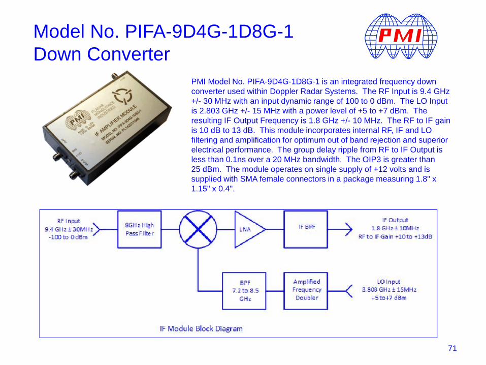
Model No. PIFA-9D4G-1D8G-1Down Converter
PMI Model No. PIFA-9D4G-1D8G-1 is an integrated frequency down converter used within Doppler Radar Systems. The RF Input is 9.4 GHz +/- 30 MHz with an input dynamic range of 100 to 0 dBm. The LO Input is 2.803 GHz +/- 15 MHz with a power level of +5 to +7 dBm. The resulting IF Output Frequency is 1.8 GHz +/- 10 MHz. The RF to IF gain is 10 dB to 13 dB. This module incorporates internal RF, IF and LO filtering and amplification for optimum out of band rejection and superior electrical performance. The group delay ripple from RF to IF Output is less than 0.1ns over a 20 MHz bandwidth. The OIP3 is greater than 25 dBm. The module operates on single supply of +12 volts and is supplied with SMA female connectors in a package measuring 1.8" x 1.15" x 0.4".
71
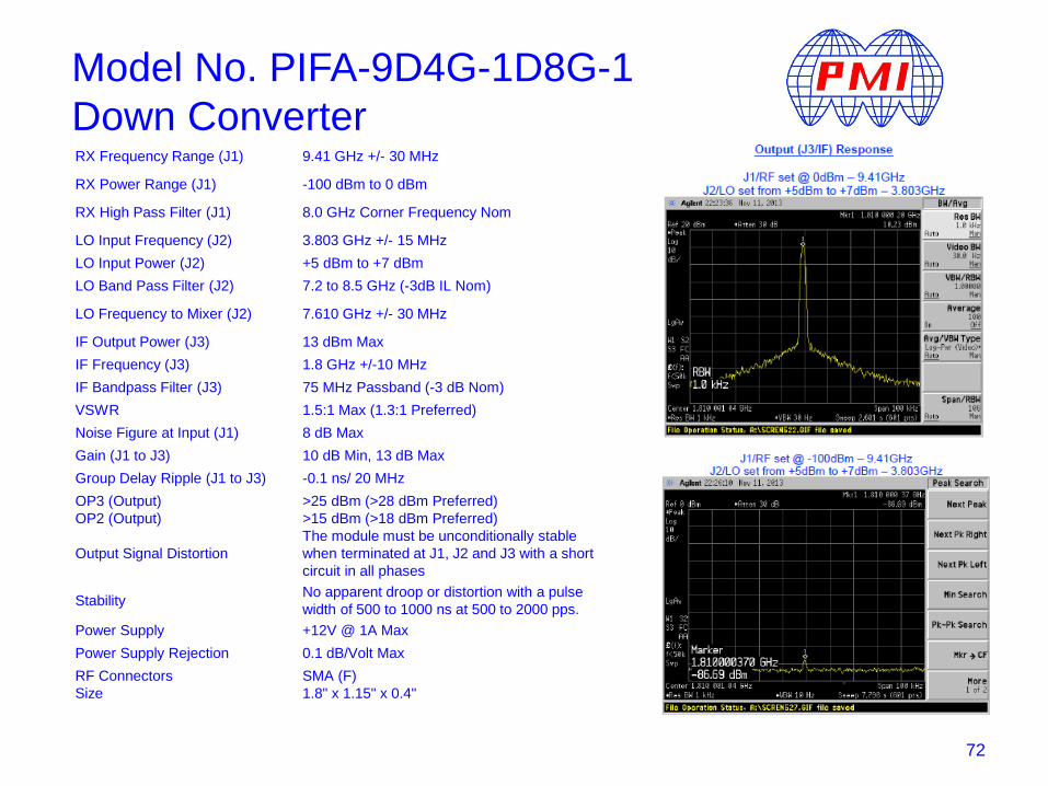
RX Frequency Range (J1) 9.41 GHz +/- 30 MHz
RX Power Range (J1) -100 dBm to 0 dBm
RX High Pass Filter (J1) 8.0 GHz Corner Frequency Nom
LO Input Frequency (J2) 3.803 GHz +/- 15 MHzLO Input Power (J2) +5 dBm to +7 dBmLO Band Pass Filter (J2) 7.2 to 8.5 GHz (-3dB IL Nom)
LO Frequency to Mixer (J2) 7.610 GHz +/- 30 MHz
IF Output Power (J3) 13 dBm MaxIF Frequency (J3) 1.8 GHz +/-10 MHzIF Bandpass Filter (J3) 75 MHz Passband (-3 dB Nom)VSWR 1.5:1 Max (1.3:1 Preferred)Noise Figure at Input (J1) 8 dB MaxGain (J1 to J3) 10 dB Min, 13 dB MaxGroup Delay Ripple (J1 to J3) -0.1 ns/ 20 MHzOP3 (Output) >25 dBm (>28 dBm Preferred)OP2 (Output) >15 dBm (>18 dBm Preferred)
Output Signal DistortionThe module must be unconditionally stable when terminated at J1, J2 and J3 with a short circuit in all phases
Stability No apparent droop or distortion with a pulse width of 500 to 1000 ns at 500 to 2000 pps.
Power Supply +12V @ 1A MaxPower Supply Rejection 0.1 dB/Volt MaxRF Connectors SMA (F)Size 1.8" x 1.15" x 0.4"
72
Model No. PIFA-9D4G-1D8G-1Down Converter

Model No. PTRAN-100M18G-70-MAH0.1 to 18.0 GHz, Transciever (PHASE I)PMI Model No. PTRAN-100M18G-70-MAH is a transceiver covering the frequency range of 100 MHz to 18.0 GHz. This unit up-converts a 100MHz to 4.0 GHz transmit signal to the 2.0 to 18.0 GHz frequency range. It also down-converts a 100 MHz to 18.0 GHz received signal to the 100 MHz to 4.0 GHz intermediate frequency range for analog to digital conversion.
73

Frequency 100MHz to 18.0 GHzInputs J3, J5, J7, J8J3 Input Input from RX Filter BankFrequency 100 MHz to 18.0 GHz
Power Level -74 dBm to -4 dBm +/-3 dBm(Assuming 6 dB +/-3.5 dB Gain in RX Filter Bank)
J5 Input IF Input from BackplaneFrequency 100 MHz to 4.0 GHzPower Level 0d Bm Typ
J7 Input LO1 from BackplaneFrequency 4.0 GHz to 20 GHzPower Level +15 dBm Typ
J8 Input LO2 from the BackplaneFrequency 4.0 GHz to 20 GHzPower Level +15 dBm Typ
Outputs J2, J4, J6J2 Output to TX Filter BankFrequency 100 MHz to 18.0 GHz
Power Level Undefined (Allow for 0 to +10 dBm Out of TX Filter Bank)
J4 IF Output to BackplaneFrequency 100 MHz to 4.0 GHzPower Level 0 dBm Typ for Non-Linear SDLVA Channels
J6 Input to RS Filter BankFrequency 100 MHz to 18.0 GHzPower Level Undefined
Control Logic LVDSPower Supplies +12V, -12V, +5V, +3.3VSize 5.55" x 3.68" x 0.89"RF Connectors SMA(F)
74
Model No. PTRAN-100M18G-70-MAH0.1 to 18.0 GHz, Transciever (PHASE I)

75
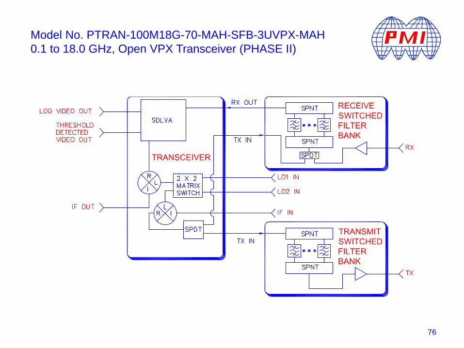
Model No. PTRAN-100M18G-70-MAH-SFB-3UVPX-MAH0.1 to 18.0 GHz, Open VPX Transceiver (PHASE II)
PMI Model No. PTRAN-100M18G-70-MAH is a transceiver covering the frequency range of 100 MHz to 18.0 GHz. This unit up-converts a 100MHz to 4.0 GHz transmit signal to the 2.0 to 18.0 GHz frequency range. It also down-converts a 100 MHz to 18.0 GHz received signal to the 100 MHz to 4.0 GHz intermediate frequency range for analog to digital conversion. This is supplied in Open VPX architecture.
76
Model No. PTRAN-100M18G-70-MAH-SFB-3UVPX-MAH0.1 to 18.0 GHz, Open VPX Transceiver (PHASE II)

Frequency 100MHz to 18.0 GHzInputs J3, J5, J7, J8
J3 Input Input from RX Filter BankFrequency 100 MHz to 18.0 GHz
Power Level -74 dBm to -4 dBm +/-3 dBm (AssuMing 6 dB +/-3.5 dB Gain in RX Filter Bank)
J5 Input IF Input from BackplaneFrequency 100 MHz to 4.0 GHzPower Level 0d Bm Typ
J7 Input LO1 from BackplaneFrequency 4.0 GHz to 20 GHzPower Level +15 dBm Typ
J8 Input LO2 from the BackplaneFrequency 4.0 GHz to 20 GHzPower Level +15 dBm Typ
Outputs J2, J4, J6J2 Output to TX Filter BankFrequency 100 MHz to 18.0 GHzPower Level Undefined (Allow for 0 to +10 dBm Out of TX Filter Bank)
J4 IF Output to BackplaneFrequency 100 MHz to 4.0 GHzPower Level 0 dBm Typ for Non-Linear SDLVA Channels
J6 Input to RS Filter BankFrequency 100 MHz to 18.0 GHzPower Level Undefined
Control Logic LVDSPower Supplies +12V, -12V, +5V, +3.3VSize 5.55" x 3.68" x 0.89"RF Connectors SMA(F)
Digital Connectors 30 Pin Headers to Connect to inrevium TB-FMCL-PH Board
FinishPainted Gray - Epoxy Polomide Coating IAW MIL-C-22750, Type I over Epoxy Polomide Primer IAW MIL-P-23377, Type I, Class 1 or 3N
Operating Temperature -40 °C to +85 ºC
77
Model No. PTRAN-100M18G-70-MAH-SFB-3UVPX-MAH0.1 to 18.0 GHz, Open VPX Transceiver (PHASE II)

78
Model No. PTRAN-100M18G-70-MAH-SFB-3UVPX-MAH0.1 to 18.0 GHz, Open VPX Transceiver (PHASE II)
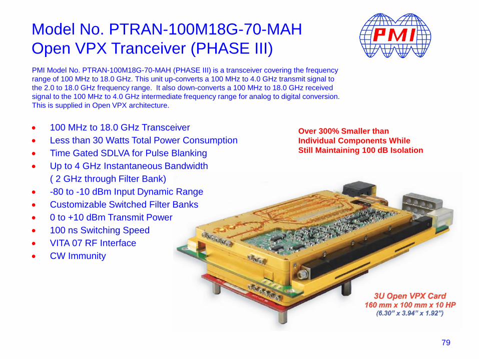
Model No. PTRAN-100M18G-70-MAHOpen VPX Tranceiver (PHASE III)PMI Model No. PTRAN-100M18G-70-MAH (PHASE III) is a transceiver covering the frequency range of 100 MHz to 18.0 GHz. This unit up-converts a 100 MHz to 4.0 GHz transmit signal to the 2.0 to 18.0 GHz frequency range. It also down-converts a 100 MHz to 18.0 GHz received signal to the 100 MHz to 4.0 GHz intermediate frequency range for analog to digital conversion. This is supplied in Open VPX architecture.
79
• 100 MHz to 18.0 GHz Transceiver• Less than 30 Watts Total Power Consumption• Time Gated SDLVA for Pulse Blanking• Up to 4 GHz Instantaneous Bandwidth
( 2 GHz through Filter Bank)• -80 to -10 dBm Input Dynamic Range• Customizable Switched Filter Banks• 0 to +10 dBm Transmit Power• 100 ns Switching Speed• VITA 07 RF Interface• CW Immunity
Over 300% Smaller thanIndividual Components WhileStill Maintaining 100 dB Isolation

80
Frequency 100 MHz to 18.0 GHzGain 18 dB TypIsolation J1, J6 100 dBSwitching Speed 100 nsInputs J1, J6
J1 Input: Input from BackplaneFrequency 100 MHz to 18.0 GHzPower Level -80 dBm to -10 dBm
J6 Input Output to TransceiverFrequency 100 Mhz to 18.0 GHzPower Level -52 dBm to -22 dBm
Outputs J3J3 Output: Output to Transceiver
Frequency 100 MHz to 18.0 GHzPower Level -74 dBm to -4dBm Typ
Thru Channel Passband 100 MHz to 18.0 GHz
Number of Filter Channels 5 Channels (2.4 – 4.4 GHz, 4.4 – 6.4 GHz, 6.4 - 8.4 GHz,8.4 – 10.4 GHz & 10.4 – 12.4 GHz)
Channel 1 Center Frequency 3400 MHz3 dB Bandwidth 2000 MHz
Rejection -40 dBc, Typ (100MHz to 2GHz), -30 dBc Min-40 dBc Typ (4.8 to 8.5GHz), -30 dBc Min
Channel 2 Center Frequency 5400 MHz3 dB Bandwidth 2000 MHz
Rejection -40 dBc Typ (100 MHz to 4 GHz), -30 dBc Min-40 dBc Typ (6.8 to 13.5 GHz), -30 dBc Min
Channel 3 Center Frequency 7400 MHz3dB Bandwidth 2000 MHz
Rejection -40 dBc Typ (100 MHz to 6 GHz), -30 dBc Min-40 dBc Typ (8.8 to 18 GHz), -30 dBc Min
Channel 4 Center Frequency 9400 MHz3 dB Bandwidth 2000 MHz
Rejection -40 dBc Typ (100 MHz to 8 GHz), -30 dBc Min-40 dBc Typ (10.8 to 18 GHz), -30 dBc Min
Channel 5 Center Frequency 11400 MHz3 dB Bandwidth 2000 MHz
Rejection -40 dBc Typ (100 MHz to 10 GHz), -30 dBc Min-40 dBc Typ (12.8 to 18GHz), -30 dBc Min
Control Logic 3.3 V TTLPower +12V, -12V, +5V, +3.3VConnectors SMA (F)Digital/Power Connector 15PIN Micro-D Mating Connector ProvidedSize 4.925" x 3.68" x 0,35"Finish Painted GrayOperating Temperature -40°C to +85 °C
Model No. PTRAN-100M18G-70-MAHOpen VPX Tranceiver (PHASE III)

81
PHASE III TRANSCEIVER FULLY ASSEMBLED
PHASE III TRANSCEIVER RECEIVE SIDE SWITCH FILTER BANK
PHASE III TRANSCEIVER TRANSMIT SIDE SWITCH FILTER BANK
Model No. PTRAN-100M18G-70-MAHOpen VPX Tranceiver (PHASE III)

82
Model No. PTRAN-100M18G-70-MAHOpen VPX Tranceiver (PHASE III)

6 - SINGLE SIDEBAND MODULATORS
83

Model No. PSM-0R5G2R5G-CD-10.5 to 2.5 GHz, Single Side-Band Modulator
• 0.5 to 2.5 GHz• 13.5 dB Max Conversion Loss• 20 dBc Carrier Suppression• 5 dBm Typ OP1dB• 2:1 VSWR• ±10° Quadrature Phase Accuracy
INPUT PARAMETERS:• RF Carrier: 0.5 to 2.5 GHz• RF VSWR (RF= -10dBm, IF Modulation +10 dBm: 2.0:1 Typ• RF Power at 1 dB Compression Point (IF=+10 dBm): +5 dBm Typ• IF Modulation Frequency Range: DC to 500 MHz• IF Modulation Power Range (50Ω): +7 dBm Min, +13 dBm Max
Transfer Characteristics:• Conversion Loss: 13.5 dB Max (See Note #1)• Carrier Suppression: 20 dBc Min, 23 dBc Typ• Fundamental IF: 15 dBc Min Carrier: ±21F, 41F, etc.: 35 dBc Typ• Carrier ±31F: 7dBc Typ• Quadrature Phase Accuracy, I/Q Mode: ±7.5º Typ, ±10º Max• Quadrature Amplitude Accuracy: ±1.5dB Typ, ±2.0dB Max
OUTPUT PARAMETERS:• RF Frequency Range: 0.5 to 2.5GHz• RF VSWR (RF=-10 dBm, IF Modulation= +10 dBm: 4.0:1 Typ
FINISH:• Nickel Plate• Dimensions: 2.5” X 2.0” X 0.50”
Note #1: Insertion Loss relative to 0 dBm RF InputAll Other Outputs including f0 are relative to the desired upper (f0+fm) Output.
84
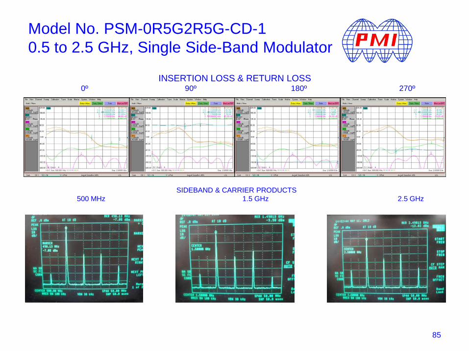
INSERTION LOSS & RETURN LOSS0º 90º 180º 270º
SIDEBAND & CARRIER PRODUCTS500 MHz 1.5 GHz 2.5 GHz
85
Model No. PSM-0R5G2R5G-CD-10.5 to 2.5 GHz, Single Side-Band Modulator

Model No. PSM-50M1G-CD-10.05 to 1.0 GHz, Single Side-Band Modulator
• 0.05 to 1.0 GHz• 10 dB Max Conversion Loss• 15 dBc Carrier Suppression• 5 dBm Typ OP1dB• 3:1 VSWR Max• ±10° Quadrature Phase Accuracy
INPUT PARAMETERS:• RF Carrier: 0.5 to 1.0 GHz• RF VSWR (RF= -10 dBm, IF Modulation +10 dBm: 2.0:1 Typ• RF Power at 1 dB Compression Point (IF=+10 dBm): +5 dBm Typ• IF Modulation Frequency Range: DC to 10 MHz• IF Modulation Power Range (50Ω): +7 dBm Min, +13 dBm Max
Transfer Characteristics:• Conversion Loss: 10 dB Max (See Note #1)• Carrier Suppression: 15 dBc Min, 20 dBc Typ• Quadrature Phase Accuracy, I/Q Mode: ±7.5º Typ, ±10º Max• Quadrature Amplitude Accuracy: ±1.5 dB Typ, ±2.0 dB Max
OUTPUT PARAMETERS:• RF Frequency Range: 0.5 to 1.0 GHz• RF VSWR (RF=-10 dBm, IF Modulation= +10 dBm: 3.0:1 Typ
FINISH:• Nickel Plate• Dimensions: 6.0” X 3.5” X 1.0”
Note #1: Insertion Loss relative to 0 dBm RF InputAll Other Outputs including f0 are relative to the desired upper (f0+fm) Output.
86

87
Model No. PSM-50M1G-CD-10.05 to 1.0 GHz, Single Side-Band Modulator

7 - SWITCH MATRICES
88

SOLID STATE SWITCH MATRIXIntegration of SP8T, 20 MHz to 3.0 GHz Switch Matrix with Integrated Power Dividers
FREQUENCY RANGE 20 – 3000 MHz
INSERTION LOSS 3.0 dB Typ
ISOLATION 55 dB Typ
VSWR 2.0:1 Max
INPUT 1dB Compression Point +25 dB Typ
SWITCHING SPEED 10 µS OFF / 20 µS ON
AMPLITUDE BALANCE ±0.25 dB
PHASE BALANCE ±4.0º
VIDEO TRANSIENTS Above 20 MHz = -100 dBmBelow 20 MHz = -75 dBm
DC POWER SUPPLY + 5 VDC @ 450 mA-12 VDC @ 250 mA
89
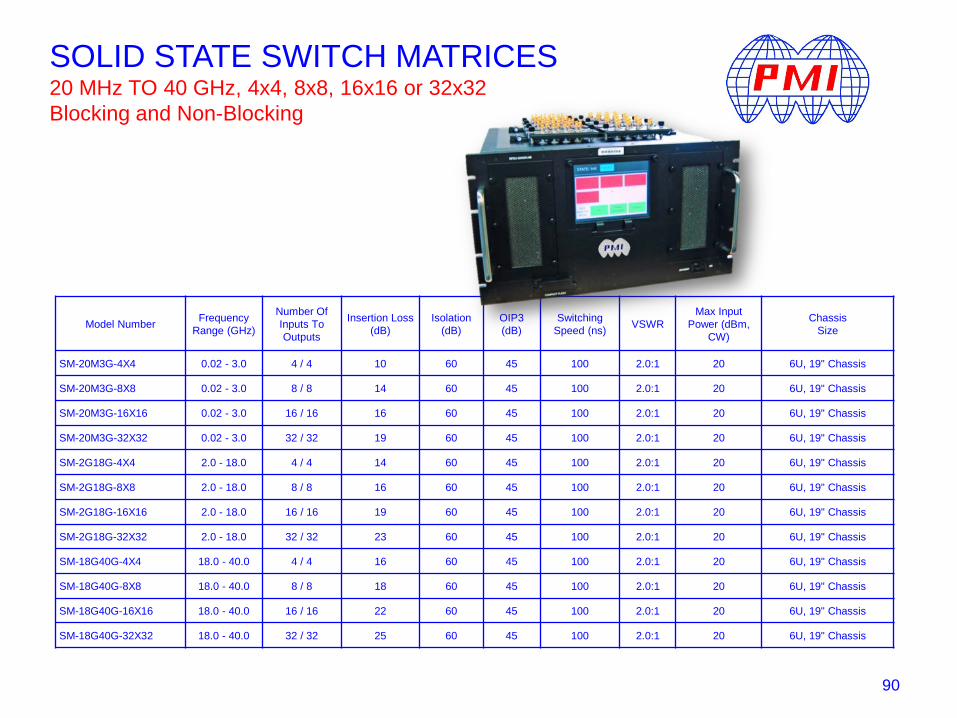
SOLID STATE SWITCH MATRICES20 MHz TO 40 GHz, 4x4, 8x8, 16x16 or 32x32Blocking and Non-Blocking
90
Model Number Frequency Range (GHz)
Number Of Inputs To Outputs
Insertion Loss(dB)
Isolation (dB)
OIP3(dB)
Switching Speed (ns) VSWR
Max Input Power (dBm,
CW)
ChassisSize
SM-20M3G-4X4 0.02 - 3.0 4 / 4 10 60 45 100 2.0:1 20 6U, 19" Chassis
SM-20M3G-8X8 0.02 - 3.0 8 / 8 14 60 45 100 2.0:1 20 6U, 19" Chassis
SM-20M3G-16X16 0.02 - 3.0 16 / 16 16 60 45 100 2.0:1 20 6U, 19" Chassis
SM-20M3G-32X32 0.02 - 3.0 32 / 32 19 60 45 100 2.0:1 20 6U, 19" Chassis
SM-2G18G-4X4 2.0 - 18.0 4 / 4 14 60 45 100 2.0:1 20 6U, 19" Chassis
SM-2G18G-8X8 2.0 - 18.0 8 / 8 16 60 45 100 2.0:1 20 6U, 19" Chassis
SM-2G18G-16X16 2.0 - 18.0 16 / 16 19 60 45 100 2.0:1 20 6U, 19" Chassis
SM-2G18G-32X32 2.0 - 18.0 32 / 32 23 60 45 100 2.0:1 20 6U, 19" Chassis
SM-18G40G-4X4 18.0 - 40.0 4 / 4 16 60 45 100 2.0:1 20 6U, 19" Chassis
SM-18G40G-8X8 18.0 - 40.0 8 / 8 18 60 45 100 2.0:1 20 6U, 19" Chassis
SM-18G40G-16X16 18.0 - 40.0 16 / 16 22 60 45 100 2.0:1 20 6U, 19" Chassis
SM-18G40G-32X32 18.0 - 40.0 32 / 32 25 60 45 100 2.0:1 20 6U, 19" Chassis

SOLID STATE SWITCH MATRICES20 MHz TO 40 GHz, 4x4, 8x8, 16x16 or 32x32Blocking and Non-Blocking
91
Switch Matrix Block Diagram
92
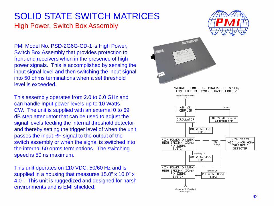
SOLID STATE SWITCH MATRICESHigh Power, Switch Box Assembly
PMI Model No. PSD-2G6G-CD-1 is High Power, Switch Box Assembly that provides protection to front-end receivers when in the presence of high power signals. This is accomplished by sensing the input signal level and then switching the input signal into 50 ohms terminations when a set threshold level is exceeded.
This assembly operates from 2.0 to 6.0 GHz and can handle input power levels up to 10 Watts CW. The unit is supplied with an external 0 to 69 dB step attenuator that can be used to adjust the signal levels feeding the internal threshold detector and thereby setting the trigger level of when the unit passes the input RF signal to the output of the switch assembly or when the signal is switched into the internal 50 ohms terminations. The switching speed is 50 ns maximum.
This unit operates on 110 VDC, 50/60 Hz and is supplied in a housing that measures 15.0” x 10.0” x 4.0”. This unit is ruggedized and designed for harsh environments and is EMI shielded.

93
SOLID STATE SWITCH MATRICESHigh Power, Switch Box Assembly
RF Input vs. RF Output