Embed Size (px)
Citation preview
Tactical Grade, Six Degrees of Freedom Inertial Sensor
Data Sheet ADIS16485
Rev. G Document Feedback Information furnished by Analog Devices is believed to be accurate and reliable. However, no responsibility is assumed by Analog Devices for its use, nor for any infringements of patents or other rights of third parties that may result from its use. Specifications subject to change without notice. No license is granted by implication or otherwise under any patent or patent rights of Analog Devices. Trademarks and registered trademarks are the property of their respective owners.
One Technology Way, P.O. Box 9106, Norwood, MA 02062-9106, U.S.A. Tel: 781.329.4700 ©2012−2017 Analog Devices, Inc. All rights reserved. Technical Support www.analog.com
FEATURES Triaxial, digital gyroscope, ±450°/sec dynamic range
±0.05° orthogonal alignment error 6°/hr in-run bias stability 0.3°/√hr angular random walk 0.01% nonlinearity
Triaxial, digital accelerometer, ±5 g Triaxial, delta angle, and delta velocity outputs Fast start-up time, ~500 ms Factory calibrated sensitivity, bias, and axial alignment
Calibration temperature range: −40°C to +85°C SPI-compatible serial interface Embedded temperature sensor Programmable operation and control
Automatic and manual bias correction controls 4 FIR filter banks, 120 configurable taps Digital I/O: data-ready alarm indicator, external clock Alarms for condition monitoring Power-down/sleep mode for power management Optional external sample clock input: up to 2.4 kHz Single command self test
Single-supply operation: 3.0 V to 3.6 V 2000 g shock survivability Operating temperature range: −40°C to +105°C
APPLICATIONS Platform stabilization and control Navigation Personnel tracking Instruments Robotics
GENERAL DESCRIPTION The ADIS16485 iSensor® device is a complete inertial system that includes a triaxial gyroscope and a triaxial accelerometer. Each inertial sensor in the ADIS16485 combines industry-leading iMEMS® technology with signal conditioning that optimizes dynamic performance. The factory calibration characterizes each sensor for sensitivity, bias, alignment, and linear acceleration (gyroscope bias). As a result, each sensor has its own dynamic compensation formulas that provide accurate sensor measurements.
The ADIS16485 provides a simple, cost-effective method for integrating accurate, multiaxis inertial sensing into industrial systems, especially when compared with the complexity and investment associated with discrete designs. All necessary motion testing and calibration are part of the production process at the factory, greatly reducing system integration time. Tight orthogonal alignment simplifies inertial frame alignment in navigation systems. The SPI and register structure provide a simple interface for data collection and configuration control.
The ADIS16485 uses the same footprint and connector system as the ADIS16375 and the ADIS16488A, which greatly simplifies the upgrade process. It comes in a module that is approximately 47 mm × 44 mm × 14 mm and has a standard connector interface.
FUNCTIONAL BLOCK DIAGRAM
CONTROLLER
CLOCK
TRIAXIALGYRO
TRIAXIALACCEL
POWERMANAGEMENT
CS
SCLK
DIN
DOUT
GND
VDD
TEMP
VDD
DIO1 DIO2 DIO3 DIO4
VDDRTC
RST
SPI
SELF TEST I/O ALARMS
OUTPUTDATA
REGISTERS
USERCONTROL
REGISTERS
CALIBRATIONAND
FILTERS
ADIS16485
1066
6-00
1
Figure 1.
ADIS16485 Data Sheet
Rev. G | Page 2 of 32
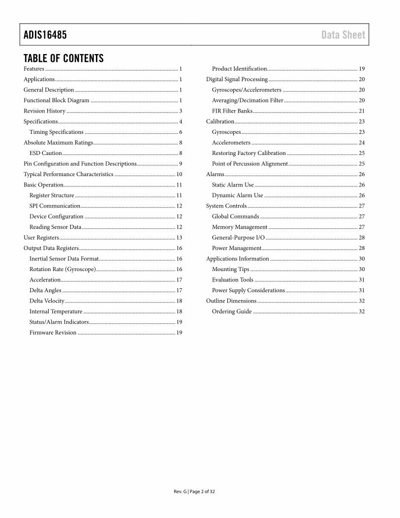
TABLE OF CONTENTS Features .............................................................................................. 1 Applications ....................................................................................... 1 General Description ......................................................................... 1 Functional Block Diagram .............................................................. 1 Revision History ............................................................................... 3 Specifications ..................................................................................... 4
Timing Specifications .................................................................. 6 Absolute Maximum Ratings ............................................................ 8
ESD Caution .................................................................................. 8 Pin Configuration and Function Descriptions ............................. 9 Typical Performance Characteristics ........................................... 10 Basic Operation............................................................................... 11
Register Structure ....................................................................... 11 SPI Communication ................................................................... 12 Device Configuration ................................................................ 12 Reading Sensor Data .................................................................. 12
User Registers .................................................................................. 13 Output Data Registers .................................................................... 16
Inertial Sensor Data Format ...................................................... 16 Rotation Rate (Gyroscope) ........................................................ 16 Acceleration ................................................................................. 17 Delta Angles ................................................................................ 17 Delta Velocity .............................................................................. 18 Internal Temperature ................................................................. 18 Status/Alarm Indicators ............................................................. 19 Firmware Revision ..................................................................... 19
Product Identification ................................................................ 19 Digital Signal Processing ............................................................... 20
Gyroscopes/Accelerometers ..................................................... 20 Averaging/Decimation Filter .................................................... 20 FIR Filter Banks .......................................................................... 21
Calibration ....................................................................................... 23 Gyroscopes .................................................................................. 23 Accelerometers ........................................................................... 24 Restoring Factory Calibration .................................................. 25 Point of Percussion Alignment ................................................. 25
Alarms .............................................................................................. 26 Static Alarm Use ......................................................................... 26 Dynamic Alarm Use .................................................................. 26
System Controls .............................................................................. 27 Global Commands ..................................................................... 27 Memory Management ............................................................... 27 General-Purpose I/O ................................................................. 28 Power Management.................................................................... 28
Applications Information .............................................................. 30 Mounting Tips ............................................................................ 30 Evaluation Tools ......................................................................... 31 Power Supply Considerations ................................................... 31
Outline Dimensions ....................................................................... 32 Ordering Guide .......................................................................... 32
Data Sheet ADIS16485
Rev. G | Page 3 of 32
REVISION HISTORY 9/2017—Rev. F to Rev. G Changed ADIS16488 to ADIS16488A ....................... Throughout Changes to Logic Inputs Parameter, Table 1 .................................. 4 Added Endnote 4, Table 1; Renumbered Sequentially ................. 5 Changed PC-Based Evaluation, EVAL-ADIS Section Title to PC-Based Evaluation, EVAL-ADIS2 Section Title ..................... 31 Changes to PC-Based Evaluation, EVAL-ADIS2 Section .......... 31 10/2016—Rev. E to Rev. F Changes to Figure 29 ...................................................................... 31 2/2015—Rev. D to Rev. E Changes to Features Section ............................................................ 1 Changes to Table 1 ............................................................................ 4 Changes to Table 2 and Figure 2 ..................................................... 6 Added Table 3; Renumbered Sequentially ..................................... 6 Change to Figure 4 ............................................................................ 7 Change to Operating Temperature Range, Table 4 ....................... 8 Change to Dual Memory Structure Section ................................ 12 Changes to Ordering Guide ........................................................... 32 5/2014—Rev. C to Rev. D Changes to Table 73, Table 74, and Table 75 ............................... 23 4/2014—Rev. B to Rev. C Change to Features Section .............................................................. 1 Moved Revision History ................................................................... 3 Added Endnote 7; Renumbered Sequentially, and Changes to Endnote 9, Table 1 ............................................................................. 5 Changes to Table 9 .......................................................................... 14 Changes to Delta Angles Section .................................................. 16 Changes to Delta Velocity Section ................................................ 17 Change to Figure 20 Caption ......................................................... 19 Changes to Linear Acceleration on Effect on Gyroscope Bias Section and Manual Bias Correction ............................................ 23 Changes to Status Alarm Use Section and Dynamic Alarm Use Section ....................................................................................... 25 Change to Software Reset Section ................................................. 26 Changes to General-Purpose I/O Section.................................... 27
12/2013—Rev. A to Rev. B Change to t2 Parameter, Table 2....................................................... 5 Change to Figure 6 ............................................................................ 7 Changes to Delta Angles Section .................................................. 15 Changes to Delta Velocity Section ................................................ 16 Changes to Status/Alarm Indicators Section ............................... 17 Deleted Prototype Interface Board Section, PC Evaluation with EVAL_ADIS Section, Mechanical Design Tips Section, Figure 26, Figure 27, Figure 30, and Figure 31; Renumbered Sequentially ..... 27 Added Mounting Tips Section and Figure 26; Renumbered Sequentially ...................................................................................... 27 Added Evaluation Tools Section, Power Supply Considerations Section, Figure 29 and Figure 30; Renumbered Sequentially ... 28 Changes to Ordering Guide ........................................................... 29 12/2012—Rev. 0 to Rev. A Changes to Table 1 ............................................................................ 3 Added tSFS Parameter, Table 2 .......................................................... 5 Changes to t2 Parameter, Table 2 and Figure 2 .............................. 5 Changes to Figure 8 .......................................................................... 8 Changes to Linear Acceleration on Effect on Gyroscope Bias Section .............................................................................................. 21 Changes to Prototype Interface Board Section ........................... 27 Deleted Installation Tips Section, and Figure 28; Renumbered Sequentially ...................................................................................... 27 Added Mechanical Design Tips Section, Connector Down Mounting Tips Section, and Figure 28; Renumbered Sequentially ...................................................................................... 27 Added Connector Up Mounting Tips Section, Figure 30, and Figure 31 ........................................................................................... 28 Updated Outline Dimensions........................................................ 29 5/2012—Revision 0: Initial Version
ADIS16485 Data Sheet
Rev. G | Page 4 of 32
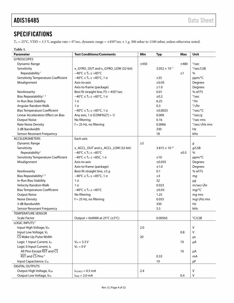
SPECIFICATIONS TA = 25°C, VDD = 3.3 V, angular rate = 0°/sec, dynamic range = ±450°/sec ± 1 g, 300 mbar to 1100 mbar, unless otherwise noted.
Table 1. Parameter Test Conditions/Comments Min Typ Max Unit GYROSCOPES
Dynamic Range ±450 ±480 °/sec Sensitivity x_GYRO_OUT and x_GYRO_LOW (32-bit) 3.052 × 10⁻⁷ °/sec/LSB
Repeatability 1 −40°C ≤ TA ≤ +85°C ±1 % Sensitivity Temperature Coefficient −40°C ≤ TA ≤ +85°C, 1 σ ±35 ppm/°C Misalignment Axis-to-axis ±0.05 Degrees Axis-to-frame (package) ±1.0 Degrees Nonlinearity Best fit straight line, FS = 450°/sec 0.01 % of FS Bias Repeatability1, 2 −40°C ≤ TA ≤ +85°C, 1 σ ±0.2 °/sec In-Run Bias Stability 1 σ 6.25 °/hr Angular Random Walk 1 σ 0.3 °/√hr Bias Temperature Coefficient −40°C ≤ TA ≤ +85°C, 1 σ ±0.0025 °/sec/°C Linear Acceleration Effect on Bias Any axis, 1 σ (CONFIG[7] = 1) 0.009 °/sec/g Output Noise No filtering 0.16 °/sec rms Rate Noise Density f = 25 Hz, no filtering 0.0066 °/sec/√Hz rms 3 dB Bandwidth 330 Hz Sensor Resonant Frequency 18 kHz
ACCELEROMETERS Each axis Dynamic Range ±5 g Sensitivity x_ACCL_OUT and x_ACCL_LOW (32-bit) 3.815 × 10⁻⁹ g/LSB
Repeatability1 −40°C ≤ TA ≤ +85°C ±0.5 % Sensitivity Temperature Coefficient −40°C ≤ TA ≤ +85C, 1 σ ±10 ppm/°C Misalignment Axis-to-axis ±0.035 Degrees Axis-to-frame (package) ±1.0 Degrees Nonlinearity Best-fit straight line, ±5 g 0.1 % of FS Bias Repeatability1, 2 −40°C ≤ TA ≤ +85°C, 1 σ ±3 mg In-Run Bias Stability 1 σ 32 µg Velocity Random Walk 1 σ 0.023 m/sec/√hr Bias Temperature Coefficient −40°C ≤ TA ≤ +85°C ±0.03 mg/°C Output Noise No filtering 1.25 mg rms Noise Density f = 25 Hz, no filtering 0.055 mg/√Hz rms 3 dB Bandwidth 330 Hz Sensor Resonant Frequency 5.5 kHz
TEMPERATURE SENSOR Scale Factor Output = 0x0000 at 25°C (±5°C) 0.00565 °C/LSB
LOGIC INPUTS 3 Input High Voltage, VIH 2.0 V Input Low Voltage, VIL 0.8 V
EE
AA Wake-Up Pulse Width CS 20 µs
Logic 1 Input Current, IIH VIH = 3.3 V 10 µA Logic 0 Input Current, IIL VIL = 0 V
All Pins Except AARST EE
AA and AACSEE 10 µA
AARST EE
AA and AACSEE
AA Pins3F3F
4 0.33 mA
Input Capacitance, CIN 10 pF DIGITAL OUTPUTS
Output High Voltage, VOH ISOURCE = 0.5 mA 2.4 V Output Low Voltage, VOL ISINK = 2.0 mA 0.4 V
Data Sheet ADIS16485
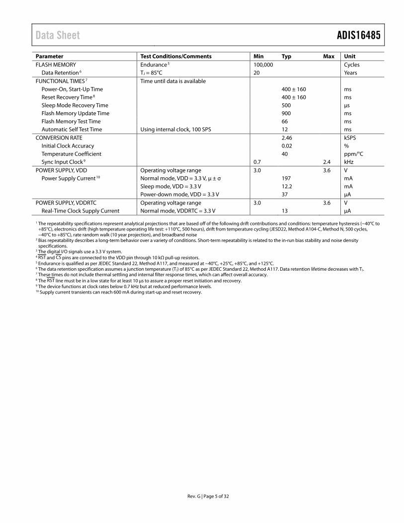
Rev. G | Page 5 of 32
Parameter Test Conditions/Comments Min Typ Max Unit FLASH MEMORY Endurance4F4F
5 100,000 Cycles Data Retention5F5F
6 TJ = 85°C 20 Years FUNCTIONAL TIMES 6F6F
7 Time until data is available Power-On, Start-Up Time 400 ± 160 ms Reset Recovery Time7F7F
8 400 ± 160 ms Sleep Mode Recovery Time 500 µs Flash Memory Update Time 900 ms Flash Memory Test Time 66 ms Automatic Self Test Time Using internal clock, 100 SPS 12 ms
CONVERSION RATE 2.46 kSPS Initial Clock Accuracy 0.02 % Temperature Coefficient 40 ppm/°C Sync Input Clock8F8F
9 0.7 2.4 kHz POWER SUPPLY, VDD Operating voltage range 3.0 3.6 V
Power Supply Current9F9F
10 Normal mode, VDD = 3.3 V, µ ± σ 197 mA Sleep mode, VDD = 3.3 V 12.2 mA
Power-down mode, VDD = 3.3 V 37 µA POWER SUPPLY, VDDRTC Operating voltage range 3.0 3.6 V
Real-Time Clock Supply Current Normal mode, VDDRTC = 3.3 V 13 µA 1 The repeatability specifications represent analytical projections that are based off of the following drift contributions and conditions: temperature hysteresis (−40°C to
+85°C), electronics drift (high temperature operating life test: +110°C, 500 hours), drift from temperature cycling (JESD22, Method A104-C, Method N, 500 cycles, −40°C to +85°C), rate random walk (10 year projection), and broadband noise
2 Bias repeatability describes a long-term behavior over a variety of conditions. Short-term repeatability is related to the in-run bias stability and noise density specifications.
3 The digital I/O signals use a 3.3 V system. 4 RST and CS pins are connected to the VDD pin through 10 kΩ pull-up resistors. 5 Endurance is qualified as per JEDEC Standard 22, Method A117, and measured at −40°C, +25°C, +85°C, and +125°C. 6 The data retention specification assumes a junction temperature (TJ) of 85°C as per JEDEC Standard 22, Method A117. Data retention lifetime decreases with TJ. 7 These times do not include thermal settling and internal filter response times, which can affect overall accuracy. 8 The RST line must be in a low state for at least 10 μs to assure a proper reset initiation and recovery. 9 The device functions at clock rates below 0.7 kHz but at reduced performance levels. 10 Supply current transients can reach 600 mA during start-up and reset recovery.
ADIS16485 Data Sheet
Rev. G | Page 6 of 32
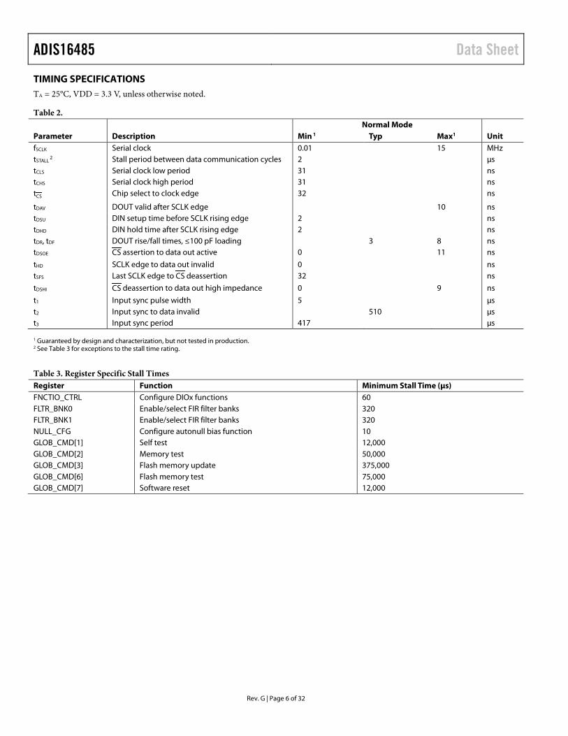
TIMING SPECIFICATIONS TA = 25°C, VDD = 3.3 V, unless otherwise noted.
Table 2. Normal Mode Parameter Description Min 10F10F
1 Typ Max1 Unit fSCLK Serial clock 0.01 15 MHz tSTALL11F11F
2 Stall period between data communication cycles 2 µs tCLS Serial clock low period 31 ns tCHS Serial clock high period 31 ns t AACS
EE Chip select to clock edge 32 ns
tDAV DOUT valid after SCLK edge 10 ns tDSU DIN setup time before SCLK rising edge 2 ns tDHD DIN hold time after SCLK rising edge 2 ns tDR, tDF DOUT rise/fall times, ≤100 pF loading 3 8 ns tDSOE AACSEE
AA assertion to data out active 0 11 ns
tHD SCLK edge to data out invalid 0 ns tSFS Last SCLK edge to AACSEE
AA deassertion 32 ns
tDSHI AACSEE
AA deassertion to data out high impedance 0 9 ns
t1 Input sync pulse width 5 µs t2 Input sync to data invalid 510 µs t3 Input sync period 417 µs 1 Guaranteed by design and characterization, but not tested in production. 2 See Table 3 for exceptions to the stall time rating.
Table 3. Register Specific Stall Times Register Function Minimum Stall Time (μs) FNCTIO_CTRL Configure DIOx functions 60 FLTR_BNK0 Enable/select FIR filter banks 320 FLTR_BNK1 Enable/select FIR filter banks 320 NULL_CFG Configure autonull bias function 10 GLOB_CMD[1] Self test 12,000 GLOB_CMD[2] Memory test 50,000 GLOB_CMD[3] Flash memory update 375,000 GLOB_CMD[6] Flash memory test 75,000 GLOB_CMD[7] Software reset 12,000
Data Sheet ADIS16485
Rev. G | Page 7 of 32
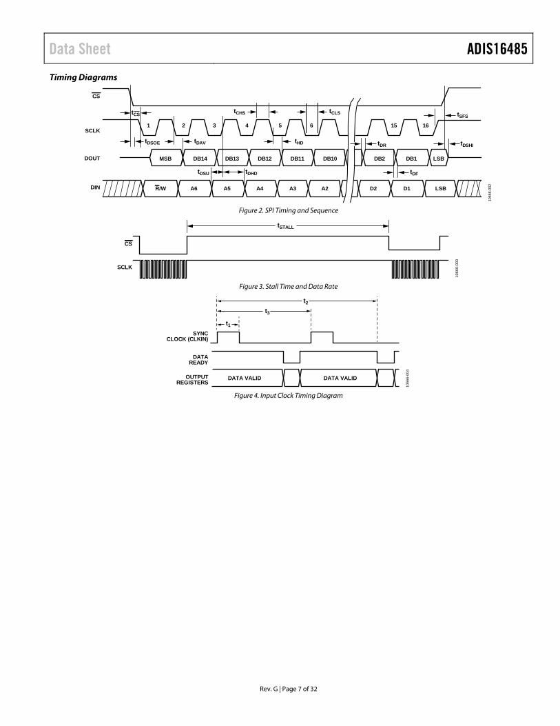
Timing Diagrams
CS
SCLK
DOUT
DIN
1 2 3 4 5 6 15 16
R/W A5A6 A4 A3 A2 D2
MSB DB14
D1 LSB
DB13 DB12 DB10DB11 DB2 LSBDB1
tCS
tDSHItDR
tSFS
tDF
tDAV tHD
tCHS tCLS
tDSOE
tDHDtDSU
1066
6-00
2
Figure 2. SPI Timing and Sequence
CS
SCLK
tSTALL
1066
6-00
3
Figure 3. Stall Time and Data Rate
t3
t2
t1
SYNCCLOCK (CLKIN)
DATAREADY
OUTPUTREGISTERS
DATA VALID DATA VALID
1066
6-00
4
Figure 4. Input Clock Timing Diagram
ADIS16485 Data Sheet
Rev. G | Page 8 of 32
ABSOLUTE MAXIMUM RATINGS Table 4. Parameter Rating Acceleration
Any Axis, Unpowered 2000 g Any Axis, Powered 2000 g
VDD to GND −0.3 V to +3.6 V Digital Input Voltage to GND −0.3 V to VDD + 0.2 V Digital Output Voltage to GND −0.3 V to VDD + 0.2 V Operating Temperature Range −40°C to +105°C Storage Temperature Range −65°C to +150°C1
1 Extended exposure to temperatures that are lower than −40°C or higher
than +105°C can adversely affect the accuracy of the factory calibration.
Stresses at or above those listed under Absolute Maximum Ratings may cause permanent damage to the product. This is a stress rating only; functional operation of the product at these or any other conditions above those indicated in the operational section of this specification is not implied. Operation beyond the maximum operating conditions for extended periods may affect product reliability.
Table 5. Package Characteristics
Package Type θJA θJC Device Weight
24-Lead Module (ML-24-6) 22.8°C/W 10.1°C/W 48 g
ESD CAUTION
Data Sheet ADIS16485
Rev. G | Page 9 of 32
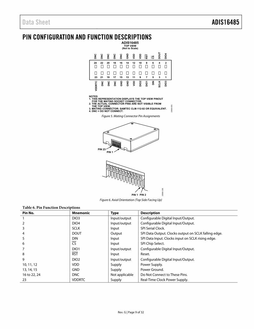
PIN CONFIGURATION AND FUNCTION DESCRIPTIONS
1
DIO
3
SC
LK
DIN
DIO
1
DIO
2
VD
D
GN
D
GN
D
DN
C
DN
C
DN
C
VD
DR
TC
DIO
4
DO
UT
CS
RS
T
VD
D
VD
D
GN
D
DN
C
DN
C
DN
C
DN
C
DN
C
2
3
4
5
6
7
8
9
10
11
12
13
14
15
16
17
18
19
20
21
22
23
24
ADIS16485TOP VIEW
(Not to Scale)
NOTES1. THIS REPRESENTATION DISPLAYS THE TOP VIEW PINOUT FOR THE MATING SOCKET CONNECTOR.2. THE ACTUAL CONNECTOR PINS ARE NOT VISIBLE FROM THE TOP VIEW.3. MATING CONNECTOR: SAMTEC CLM-112-02 OR EQUIVALENT.4. DNC = DO NOT CONNECT. 10
666-
005
Figure 5. Mating Connector Pin Assignments
PIN 1PIN 23
PIN 1 PIN 2 1066
6-10
6
Figure 6. Axial Orientation (Top Side Facing Up)
Table 6. Pin Function Descriptions Pin No. Mnemonic Type Description 1 DIO3 Input/output Configurable Digital Input/Output. 2 DIO4 Input/output Configurable Digital Input/Output. 3 SCLK Input SPI Serial Clock. 4 DOUT Output SPI Data Output. Clocks output on SCLK falling edge. 5 DIN Input SPI Data Input. Clocks input on SCLK rising edge. 6 ACS E Input SPI Chip Select.
7 DIO1 Input/output Configurable Digital Input/Output. 8 ARSTE Input Reset.
9 DIO2 Input/output Configurable Digital Input/Output. 10, 11, 12 VDD Supply Power Supply. 13, 14, 15 GND Supply Power Ground. 16 to 22, 24 DNC Not applicable Do Not Connect to These Pins. 23 VDDRTC Supply Real-Time Clock Power Supply.
ADIS16485 Data Sheet
Rev. G | Page 10 of 32
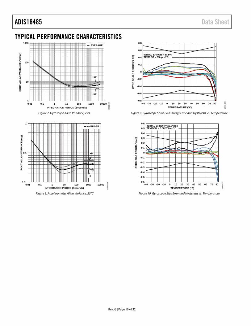
TYPICAL PERFORMANCE CHARACTERISTICS 1000
1
10
100
0.01 0.1 1 10 100 1000 10000
ROO
TAL
LAN
VARI
ANC
E(°
/Hou
r)
INTEGRATION PERIOD (Seconds)
+1σ
–1σ
AVERAGE
1066
6-00
7
Figure 7. Gyroscope Allan Variance, 25°C
0.01
0.1
1
0.01 0.1 1 10 100 1000 10000
–δ
+δ
RO
OT
ALL
AN
VAR
IAN
CE
(mg)
INTEGRATION PERIOD (Seconds) 1066
6-00
8
AVERAGE
Figure 8. Accelerometer Allan Variance, 25°C
0.8
–0.8
–0.6
–0.4
–0.2
0
0.2
0.4
0.6
–40 –30 –20 –10 0 10 20 30 40 50 60 70 80
GYR
OSC
ALE
ERRO
R(%
FS)
TEMPERATURE (°C)
INITIAL ERROR = ±0.5%TEMPCO = 35ppm/°C
1066
6-00
9
Figure 9. Gyroscope Scale (Sensitivity) Error and Hysteresis vs. Temperature
0.6
–0.6
–0.5
–0.4
–0.3
–0.2
–0.1
0
0.1
0.2
0.3
0.4
0.5
–40 –30 –20 –10 0 10 20 30 40 50 60 70 80
GYR
OB
IAS
ERR
OR
(°/s
ec)
TEMPERATURE (°C)
INITIAL ERROR = ±0.2°/secTEMPCO = 0.0025°/sec/°C
1066
6-01
0
Figure 10. Gyroscope Bias Error and Hysteresis vs. Temperature
Data Sheet ADIS16485
Rev. G | Page 11 of 32
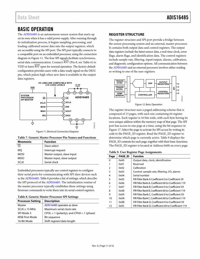
BASIC OPERATION The ADIS16485 is an autonomous sensor system that starts up on its own when it has a valid power supply. After running through its initialization process, it begins sampling, processing, and loading calibrated sensor data into the output registers, which are accessible using the SPI port. The SPI port typically connects to a compatible port on an embedded processor, using the connection diagram in Figure 11. The four SPI signals facilitate synchronous, serial data communication. Connect A
RST E
A (Pin 8, see Table 6) to VDD or leave A
RSTE
A open for normal operation. The factory default configuration provides users with a data-ready signal on the DIO2 pin, which pulses high when new data is available in the output data registers.
SYSTEMPROCESSORSPI MASTER
SCLK
CS
DIN
DOUT
SCLK
SS
MOSI
MISO
+3.3V
IRQ DIO2
VDD
I/O LINES ARE COMPATIBLE WITH3.3V LOGIC LEVELS
10
6
3
5
4
9
11 12 23
13 14 15
ADIS1648510
666-
011
Figure 11. Electrical Connection Diagram
Table 7. Generic Master Processor Pin Names and Functions Mnemonic Function ASS E Slave select
IRQ Interrupt request MOSI Master output, slave input MISO Master input, slave output SCLK Serial clock
Embedded processors typically use control registers to configure their serial ports for communicating with SPI slave devices such as the ADIS16485. Table 8 provides a list of settings, which describe the SPI protocol of the ADIS16485. The initialization routine of the master processor typically establishes these settings using firmware commands to write them into its serial control registers.
Table 8. Generic Master Processor SPI Settings Processor Setting Description Master ADIS16485 operates as slave SCLK ≤ 15 MHz Maximum serial clock rate SPI Mode 3 CPOL = 1 (polarity), and CPHA = 1 (phase) MSB-First Mode Bit sequence 16-Bit Mode Shift register/data length
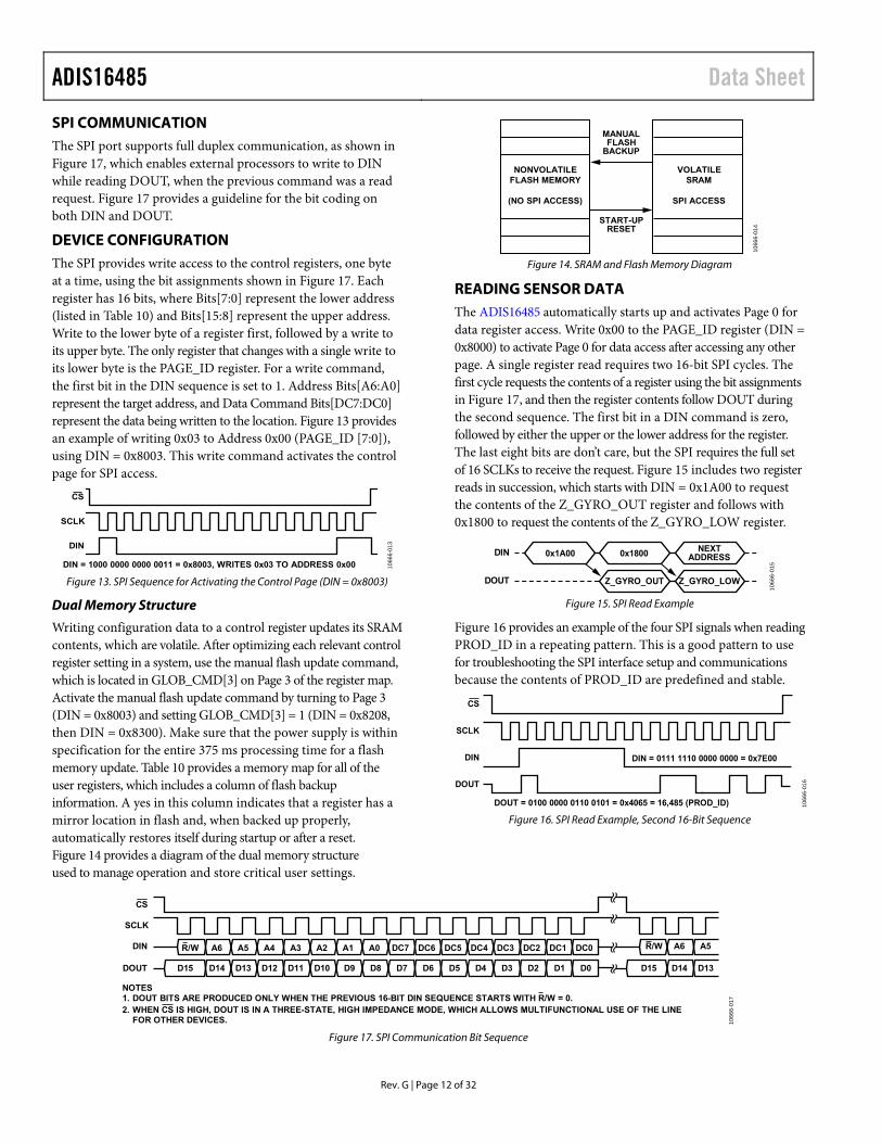
REGISTER STRUCTURE The register structure and SPI port provide a bridge between the sensor processing system and an external, master processor. It contains both output data and control registers. The output data registers include the latest sensor data, a real-time clock, error flags, alarm flags, and identification data. The control registers include sample rate, filtering, input/output, alarms, calibration, and diagnostic configuration options. All communication between the ADIS16485 and an external processor involves either reading or writing to one of the user registers.
TRIAXISGYRO
TEMPSENSOR
TRIAXISACCEL
DSPOUTPUT
REGISTERS
CONTROLREGISTERS
CONTROLLER
SP
I
1066
6-01
2
Figure 12. Basic Operation
The register structure uses a paged addressing scheme that is composed of 13 pages, with each one containing 64 register locations. Each register is 16 bits wide, with each byte having its own unique address within the memory map of that page. The SPI port has access to one page at a time, using the bit sequence in Figure 17. Select the page to activate for SPI access by writing its code to the PAGE_ID register. Read the PAGE_ID register to determine which page is currently active. Table 9 displays the PAGE_ID contents for each page, together with their basic functions. The PAGE_ID register is located at Address 0x00 on every page.
Table 9. User Register Page Assignments Page PAGE_ID Function 0 0x00 Output data, clock, identification 1 0x01 Reserved 2 0x02 Calibration 3 0x03 Control: sample rate, filtering, I/O, alarms 4 0x04 Serial number 5 0x05 FIR Filter Bank A Coefficient 0 to Coefficient 59 6 0x06 FIR Filter Bank A, Coefficient 60 to Coefficient 119 7 0x07 FIR Filter Bank B, Coefficient 0 to Coefficient 59 8 0x08 FIR Filter Bank B, Coefficient 60 to Coefficient 119 9 0x09 FIR Filter Bank C, Coefficient 0 to Coefficient 59 10 0x0A FIR Filter Bank C, Coefficient 60 to Coefficient 119 11 0x0B FIR Filter Bank D, Coefficient 0 to Coefficient 59 12 0x0C FIR Filter Bank D, Coefficient 60 to Coefficient 119
ADIS16485 Data Sheet
Rev. G | Page 12 of 32
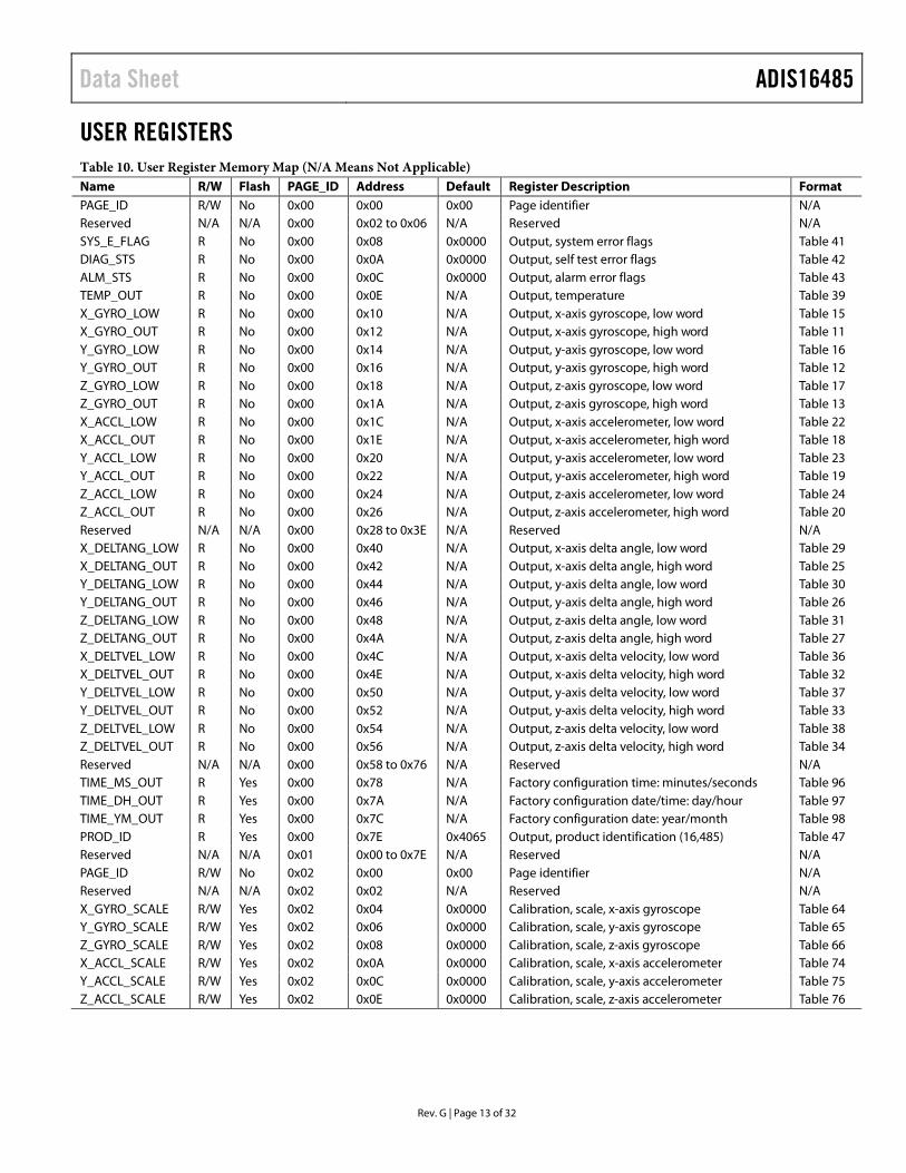
SPI COMMUNICATION The SPI port supports full duplex communication, as shown in Figure 17, which enables external processors to write to DIN while reading DOUT, when the previous command was a read request. Figure 17 provides a guideline for the bit coding on both DIN and DOUT.
DEVICE CONFIGURATION The SPI provides write access to the control registers, one byte at a time, using the bit assignments shown in Figure 17. Each register has 16 bits, where Bits[7:0] represent the lower address (listed in Table 10) and Bits[15:8] represent the upper address. Write to the lower byte of a register first, followed by a write to its upper byte. The only register that changes with a single write to its lower byte is the PAGE_ID register. For a write command, the first bit in the DIN sequence is set to 1. Address Bits[A6:A0] represent the target address, and Data Command Bits[DC7:DC0] represent the data being written to the location. Figure 13 provides an example of writing 0x03 to Address 0x00 (PAGE_ID [7:0]), using DIN = 0x8003. This write command activates the control page for SPI access.
SCLK
CS
DIN
DIN = 1000 0000 0000 0011 = 0x8003, WRITES 0x03 TO ADDRESS 0x00 1066
6-01
3
Figure 13. SPI Sequence for Activating the Control Page (DIN = 0x8003)
Dual Memory Structure
Writing configuration data to a control register updates its SRAM contents, which are volatile. After optimizing each relevant control register setting in a system, use the manual flash update command, which is located in GLOB_CMD[3] on Page 3 of the register map. Activate the manual flash update command by turning to Page 3 (DIN = 0x8003) and setting GLOB_CMD[3] = 1 (DIN = 0x8208, then DIN = 0x8300). Make sure that the power supply is within specification for the entire 375 ms processing time for a flash memory update. Table 10 provides a memory map for all of the user registers, which includes a column of flash backup information. A yes in this column indicates that a register has a mirror location in flash and, when backed up properly, automatically restores itself during startup or after a reset. Figure 14 provides a diagram of the dual memory structure used to manage operation and store critical user settings.
NONVOLATILEFLASH MEMORY
(NO SPI ACCESS)
MANUALFLASH
BACKUP
START-UPRESET
VOLATILESRAM
SPI ACCESS
1066
6-01
4
Figure 14. SRAM and Flash Memory Diagram
READING SENSOR DATA The ADIS16485 automatically starts up and activates Page 0 for data register access. Write 0x00 to the PAGE_ID register (DIN = 0x8000) to activate Page 0 for data access after accessing any other page. A single register read requires two 16-bit SPI cycles. The first cycle requests the contents of a register using the bit assignments in Figure 17, and then the register contents follow DOUT during the second sequence. The first bit in a DIN command is zero, followed by either the upper or the lower address for the register. The last eight bits are don’t care, but the SPI requires the full set of 16 SCLKs to receive the request. Figure 15 includes two register reads in succession, which starts with DIN = 0x1A00 to request the contents of the Z_GYRO_OUT register and follows with 0x1800 to request the contents of the Z_GYRO_LOW register.
DIN
DOUT
0x1A00 0x1800 NEXTADDRESS
Z_GYRO_OUT Z_GYRO_LOW
1066
6-01
5
Figure 15. SPI Read Example
Figure 16 provides an example of the four SPI signals when reading PROD_ID in a repeating pattern. This is a good pattern to use for troubleshooting the SPI interface setup and communications because the contents of PROD_ID are predefined and stable.
SCLK
CS
DIN
DOUT
DOUT = 0100 0000 0110 0101 = 0x4065 = 16,485 (PROD_ID)
DIN = 0111 1110 0000 0000 = 0x7E00
1066
6-01
6
Figure 16. SPI Read Example, Second 16-Bit Sequence
R/W R/WA6 A5 A4 A3 A2 A1 A0 DC7 DC6 DC5 DC4 DC3 DC2 DC1 DC0
D0D1D2D3D4D5D6D7D8D9D10D11D12D13D14D15
CS
SCLK
DIN
DOUT
A6 A5
D13D14D15
NOTES1. DOUT BITS ARE PRODUCED ONLY WHEN THE PREVIOUS 16-BIT DIN SEQUENCE STARTS WITH R/W = 0.2. WHEN CS IS HIGH, DOUT IS IN A THREE-STATE, HIGH IMPEDANCE MODE, WHICH ALLOWS MULTIFUNCTIONAL USE OF THE LINE
FOR OTHER DEVICES. 1066
6-01
7
Figure 17. SPI Communication Bit Sequence
Data Sheet ADIS16485
Rev. G | Page 13 of 32
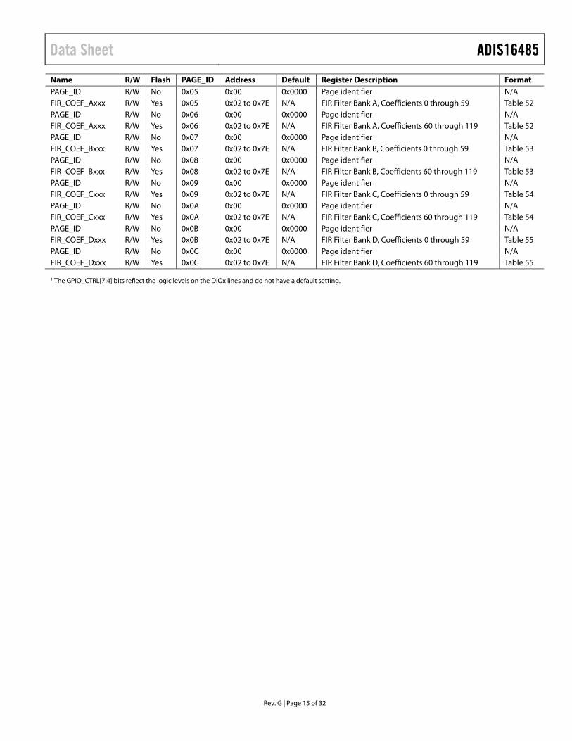
USER REGISTERS Table 10. User Register Memory Map (N/A Means Not Applicable) Name R/W Flash PAGE_ID Address Default Register Description Format PAGE_ID R/W No 0x00 0x00 0x00 Page identifier N/A Reserved N/A N/A 0x00 0x02 to 0x06 N/A Reserved N/A SYS_E_FLAG R No 0x00 0x08 0x0000 Output, system error flags Table 41 DIAG_STS R No 0x00 0x0A 0x0000 Output, self test error flags Table 42 ALM_STS R No 0x00 0x0C 0x0000 Output, alarm error flags Table 43 TEMP_OUT R No 0x00 0x0E N/A Output, temperature Table 39 X_GYRO_LOW R No 0x00 0x10 N/A Output, x-axis gyroscope, low word Table 15 X_GYRO_OUT R No 0x00 0x12 N/A Output, x-axis gyroscope, high word Table 11 Y_GYRO_LOW R No 0x00 0x14 N/A Output, y-axis gyroscope, low word Table 16 Y_GYRO_OUT R No 0x00 0x16 N/A Output, y-axis gyroscope, high word Table 12 Z_GYRO_LOW R No 0x00 0x18 N/A Output, z-axis gyroscope, low word Table 17 Z_GYRO_OUT R No 0x00 0x1A N/A Output, z-axis gyroscope, high word Table 13 X_ACCL_LOW R No 0x00 0x1C N/A Output, x-axis accelerometer, low word Table 22 X_ACCL_OUT R No 0x00 0x1E N/A Output, x-axis accelerometer, high word Table 18 Y_ACCL_LOW R No 0x00 0x20 N/A Output, y-axis accelerometer, low word Table 23 Y_ACCL_OUT R No 0x00 0x22 N/A Output, y-axis accelerometer, high word Table 19 Z_ACCL_LOW R No 0x00 0x24 N/A Output, z-axis accelerometer, low word Table 24 Z_ACCL_OUT R No 0x00 0x26 N/A Output, z-axis accelerometer, high word Table 20 Reserved N/A N/A 0x00 0x28 to 0x3E N/A Reserved N/A X_DELTANG_LOW R No 0x00 0x40 N/A Output, x-axis delta angle, low word Table 29 X_DELTANG_OUT R No 0x00 0x42 N/A Output, x-axis delta angle, high word Table 25 Y_DELTANG_LOW R No 0x00 0x44 N/A Output, y-axis delta angle, low word Table 30 Y_DELTANG_OUT R No 0x00 0x46 N/A Output, y-axis delta angle, high word Table 26 Z_DELTANG_LOW R No 0x00 0x48 N/A Output, z-axis delta angle, low word Table 31 Z_DELTANG_OUT R No 0x00 0x4A N/A Output, z-axis delta angle, high word Table 27 X_DELTVEL_LOW R No 0x00 0x4C N/A Output, x-axis delta velocity, low word Table 36 X_DELTVEL_OUT R No 0x00 0x4E N/A Output, x-axis delta velocity, high word Table 32 Y_DELTVEL_LOW R No 0x00 0x50 N/A Output, y-axis delta velocity, low word Table 37 Y_DELTVEL_OUT R No 0x00 0x52 N/A Output, y-axis delta velocity, high word Table 33 Z_DELTVEL_LOW R No 0x00 0x54 N/A Output, z-axis delta velocity, low word Table 38 Z_DELTVEL_OUT R No 0x00 0x56 N/A Output, z-axis delta velocity, high word Table 34 Reserved N/A N/A 0x00 0x58 to 0x76 N/A Reserved N/A TIME_MS_OUT R Yes 0x00 0x78 N/A Factory configuration time: minutes/seconds Table 96 TIME_DH_OUT R Yes 0x00 0x7A N/A Factory configuration date/time: day/hour Table 97 TIME_YM_OUT R Yes 0x00 0x7C N/A Factory configuration date: year/month Table 98 PROD_ID R Yes 0x00 0x7E 0x4065 Output, product identification (16,485) Table 47 Reserved N/A N/A 0x01 0x00 to 0x7E N/A Reserved N/A PAGE_ID R/W No 0x02 0x00 0x00 Page identifier N/A Reserved N/A N/A 0x02 0x02 N/A Reserved N/A X_GYRO_SCALE R/W Yes 0x02 0x04 0x0000 Calibration, scale, x-axis gyroscope Table 64 Y_GYRO_SCALE R/W Yes 0x02 0x06 0x0000 Calibration, scale, y-axis gyroscope Table 65 Z_GYRO_SCALE R/W Yes 0x02 0x08 0x0000 Calibration, scale, z-axis gyroscope Table 66 X_ACCL_SCALE R/W Yes 0x02 0x0A 0x0000 Calibration, scale, x-axis accelerometer Table 74 Y_ACCL_SCALE R/W Yes 0x02 0x0C 0x0000 Calibration, scale, y-axis accelerometer Table 75 Z_ACCL_SCALE R/W Yes 0x02 0x0E 0x0000 Calibration, scale, z-axis accelerometer Table 76
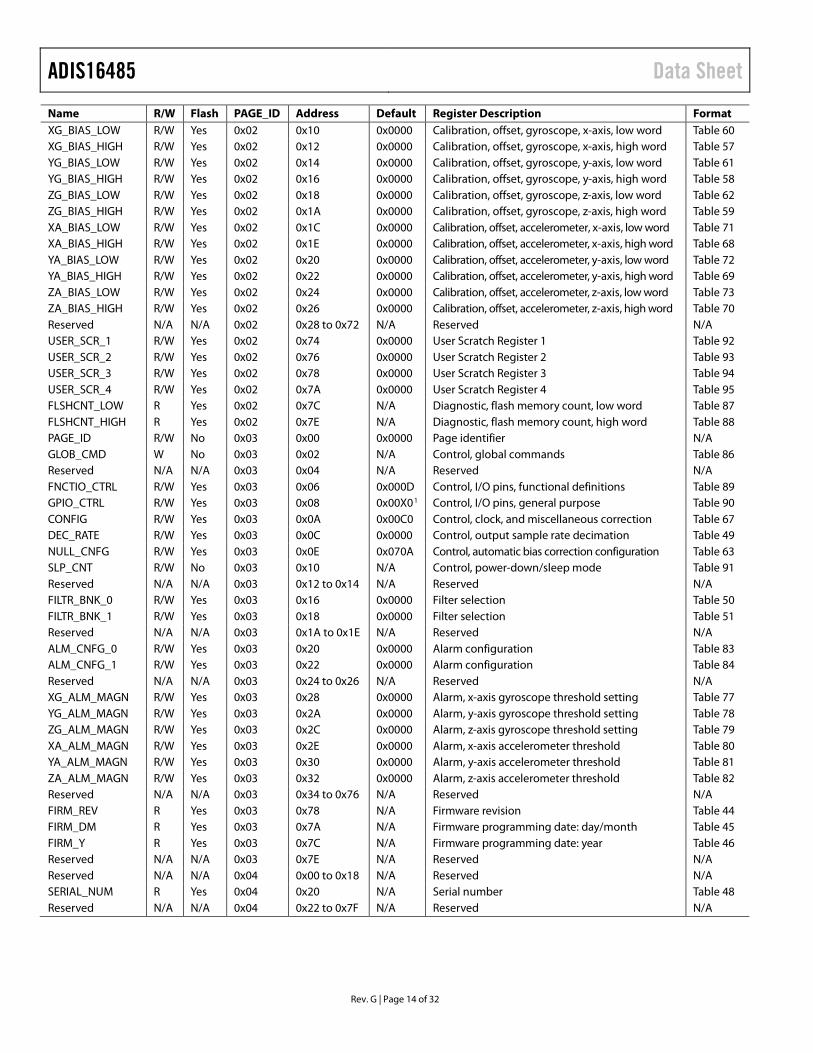
ADIS16485 Data Sheet
Rev. G | Page 14 of 32
Name R/W Flash PAGE_ID Address Default Register Description Format XG_BIAS_LOW R/W Yes 0x02 0x10 0x0000 Calibration, offset, gyroscope, x-axis, low word Table 60 XG_BIAS_HIGH R/W Yes 0x02 0x12 0x0000 Calibration, offset, gyroscope, x-axis, high word Table 57 YG_BIAS_LOW R/W Yes 0x02 0x14 0x0000 Calibration, offset, gyroscope, y-axis, low word Table 61 YG_BIAS_HIGH R/W Yes 0x02 0x16 0x0000 Calibration, offset, gyroscope, y-axis, high word Table 58 ZG_BIAS_LOW R/W Yes 0x02 0x18 0x0000 Calibration, offset, gyroscope, z-axis, low word Table 62 ZG_BIAS_HIGH R/W Yes 0x02 0x1A 0x0000 Calibration, offset, gyroscope, z-axis, high word Table 59 XA_BIAS_LOW R/W Yes 0x02 0x1C 0x0000 Calibration, offset, accelerometer, x-axis, low word Table 71 XA_BIAS_HIGH R/W Yes 0x02 0x1E 0x0000 Calibration, offset, accelerometer, x-axis, high word Table 68 YA_BIAS_LOW R/W Yes 0x02 0x20 0x0000 Calibration, offset, accelerometer, y-axis, low word Table 72 YA_BIAS_HIGH R/W Yes 0x02 0x22 0x0000 Calibration, offset, accelerometer, y-axis, high word Table 69 ZA_BIAS_LOW R/W Yes 0x02 0x24 0x0000 Calibration, offset, accelerometer, z-axis, low word Table 73 ZA_BIAS_HIGH R/W Yes 0x02 0x26 0x0000 Calibration, offset, accelerometer, z-axis, high word Table 70 Reserved N/A N/A 0x02 0x28 to 0x72 N/A Reserved N/A USER_SCR_1 R/W Yes 0x02 0x74 0x0000 User Scratch Register 1 Table 92 USER_SCR_2 R/W Yes 0x02 0x76 0x0000 User Scratch Register 2 Table 93 USER_SCR_3 R/W Yes 0x02 0x78 0x0000 User Scratch Register 3 Table 94 USER_SCR_4 R/W Yes 0x02 0x7A 0x0000 User Scratch Register 4 Table 95 FLSHCNT_LOW R Yes 0x02 0x7C N/A Diagnostic, flash memory count, low word Table 87 FLSHCNT_HIGH R Yes 0x02 0x7E N/A Diagnostic, flash memory count, high word Table 88 PAGE_ID R/W No 0x03 0x00 0x0000 Page identifier N/A GLOB_CMD W No 0x03 0x02 N/A Control, global commands Table 86 Reserved N/A N/A 0x03 0x04 N/A Reserved N/A FNCTIO_CTRL R/W Yes 0x03 0x06 0x000D Control, I/O pins, functional definitions Table 89 GPIO_CTRL R/W Yes 0x03 0x08 0x00X01 Control, I/O pins, general purpose Table 90 CONFIG R/W Yes 0x03 0x0A 0x00C0 Control, clock, and miscellaneous correction Table 67 DEC_RATE R/W Yes 0x03 0x0C 0x0000 Control, output sample rate decimation Table 49 NULL_CNFG R/W Yes 0x03 0x0E 0x070A Control, automatic bias correction configuration Table 63 SLP_CNT R/W No 0x03 0x10 N/A Control, power-down/sleep mode Table 91 Reserved N/A N/A 0x03 0x12 to 0x14 N/A Reserved N/A FILTR_BNK_0 R/W Yes 0x03 0x16 0x0000 Filter selection Table 50 FILTR_BNK_1 R/W Yes 0x03 0x18 0x0000 Filter selection Table 51 Reserved N/A N/A 0x03 0x1A to 0x1E N/A Reserved N/A ALM_CNFG_0 R/W Yes 0x03 0x20 0x0000 Alarm configuration Table 83 ALM_CNFG_1 R/W Yes 0x03 0x22 0x0000 Alarm configuration Table 84 Reserved N/A N/A 0x03 0x24 to 0x26 N/A Reserved N/A XG_ALM_MAGN R/W Yes 0x03 0x28 0x0000 Alarm, x-axis gyroscope threshold setting Table 77 YG_ALM_MAGN R/W Yes 0x03 0x2A 0x0000 Alarm, y-axis gyroscope threshold setting Table 78 ZG_ALM_MAGN R/W Yes 0x03 0x2C 0x0000 Alarm, z-axis gyroscope threshold setting Table 79 XA_ALM_MAGN R/W Yes 0x03 0x2E 0x0000 Alarm, x-axis accelerometer threshold Table 80 YA_ALM_MAGN R/W Yes 0x03 0x30 0x0000 Alarm, y-axis accelerometer threshold Table 81 ZA_ALM_MAGN R/W Yes 0x03 0x32 0x0000 Alarm, z-axis accelerometer threshold Table 82 Reserved N/A N/A 0x03 0x34 to 0x76 N/A Reserved N/A FIRM_REV R Yes 0x03 0x78 N/A Firmware revision Table 44 FIRM_DM R Yes 0x03 0x7A N/A Firmware programming date: day/month Table 45 FIRM_Y R Yes 0x03 0x7C N/A Firmware programming date: year Table 46 Reserved N/A N/A 0x03 0x7E N/A Reserved N/A Reserved N/A N/A 0x04 0x00 to 0x18 N/A Reserved N/A SERIAL_NUM R Yes 0x04 0x20 N/A Serial number Table 48 Reserved N/A N/A 0x04 0x22 to 0x7F N/A Reserved N/A
Data Sheet ADIS16485
Rev. G | Page 15 of 32
Name R/W Flash PAGE_ID Address Default Register Description Format PAGE_ID R/W No 0x05 0x00 0x0000 Page identifier N/A FIR_COEF_Axxx R/W Yes 0x05 0x02 to 0x7E N/A FIR Filter Bank A, Coefficients 0 through 59 Table 52 PAGE_ID R/W No 0x06 0x00 0x0000 Page identifier N/A FIR_COEF_Axxx R/W Yes 0x06 0x02 to 0x7E N/A FIR Filter Bank A, Coefficients 60 through 119 Table 52 PAGE_ID R/W No 0x07 0x00 0x0000 Page identifier N/A FIR_COEF_Bxxx R/W Yes 0x07 0x02 to 0x7E N/A FIR Filter Bank B, Coefficients 0 through 59 Table 53 PAGE_ID R/W No 0x08 0x00 0x0000 Page identifier N/A FIR_COEF_Bxxx R/W Yes 0x08 0x02 to 0x7E N/A FIR Filter Bank B, Coefficients 60 through 119 Table 53 PAGE_ID R/W No 0x09 0x00 0x0000 Page identifier N/A FIR_COEF_Cxxx R/W Yes 0x09 0x02 to 0x7E N/A FIR Filter Bank C, Coefficients 0 through 59 Table 54 PAGE_ID R/W No 0x0A 0x00 0x0000 Page identifier N/A FIR_COEF_Cxxx R/W Yes 0x0A 0x02 to 0x7E N/A FIR Filter Bank C, Coefficients 60 through 119 Table 54 PAGE_ID R/W No 0x0B 0x00 0x0000 Page identifier N/A FIR_COEF_Dxxx R/W Yes 0x0B 0x02 to 0x7E N/A FIR Filter Bank D, Coefficients 0 through 59 Table 55 PAGE_ID R/W No 0x0C 0x00 0x0000 Page identifier N/A FIR_COEF_Dxxx R/W Yes 0x0C 0x02 to 0x7E N/A FIR Filter Bank D, Coefficients 60 through 119 Table 55 1 The GPIO_CTRL[7:4] bits reflect the logic levels on the DIOx lines and do not have a default setting.
ADIS16485 Data Sheet
Rev. G | Page 16 of 32
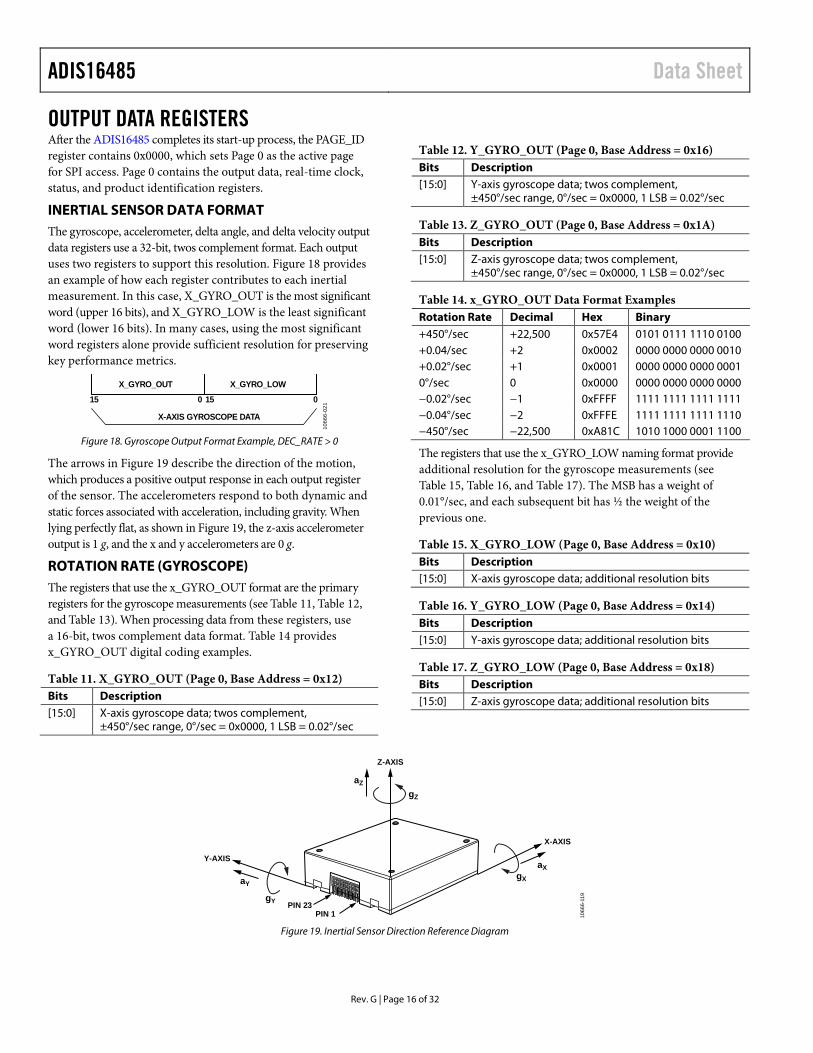
OUTPUT DATA REGISTERS After the ADIS16485 completes its start-up process, the PAGE_ID register contains 0x0000, which sets Page 0 as the active page for SPI access. Page 0 contains the output data, real-time clock, status, and product identification registers.
INERTIAL SENSOR DATA FORMAT The gyroscope, accelerometer, delta angle, and delta velocity output data registers use a 32-bit, twos complement format. Each output uses two registers to support this resolution. Figure 18 provides an example of how each register contributes to each inertial measurement. In this case, X_GYRO_OUT is the most significant word (upper 16 bits), and X_GYRO_LOW is the least significant word (lower 16 bits). In many cases, using the most significant word registers alone provide sufficient resolution for preserving key performance metrics.
1066
6-02
1
X-AXIS GYROSCOPE DATA
0 1515 0
X_GYRO_OUT X_GYRO_LOW
Figure 18. Gyroscope Output Format Example, DEC_RATE > 0
The arrows in Figure 19 describe the direction of the motion, which produces a positive output response in each output register of the sensor. The accelerometers respond to both dynamic and static forces associated with acceleration, including gravity. When lying perfectly flat, as shown in Figure 19, the z-axis accelerometer output is 1 g, and the x and y accelerometers are 0 g.
ROTATION RATE (GYROSCOPE) The registers that use the x_GYRO_OUT format are the primary registers for the gyroscope measurements (see Table 11, Table 12, and Table 13). When processing data from these registers, use a 16-bit, twos complement data format. Table 14 provides x_GYRO_OUT digital coding examples.
Table 11. X_GYRO_OUT (Page 0, Base Address = 0x12) Bits Description [15:0] X-axis gyroscope data; twos complement,
±450°/sec range, 0°/sec = 0x0000, 1 LSB = 0.02°/sec
Table 12. Y_GYRO_OUT (Page 0, Base Address = 0x16) Bits Description [15:0] Y-axis gyroscope data; twos complement,
±450°/sec range, 0°/sec = 0x0000, 1 LSB = 0.02°/sec
Table 13. Z_GYRO_OUT (Page 0, Base Address = 0x1A) Bits Description [15:0] Z-axis gyroscope data; twos complement,
±450°/sec range, 0°/sec = 0x0000, 1 LSB = 0.02°/sec
Table 14. x_GYRO_OUT Data Format Examples Rotation Rate Decimal Hex Binary +450°/sec +22,500 0x57E4 0101 0111 1110 0100 +0.04/sec +2 0x0002 0000 0000 0000 0010 +0.02°/sec +1 0x0001 0000 0000 0000 0001 0°/sec 0 0x0000 0000 0000 0000 0000 −0.02°/sec −1 0xFFFF 1111 1111 1111 1111 −0.04°/sec −2 0xFFFE 1111 1111 1111 1110 −450°/sec −22,500 0xA81C 1010 1000 0001 1100
The registers that use the x_GYRO_LOW naming format provide additional resolution for the gyroscope measurements (see Table 15, Table 16, and Table 17). The MSB has a weight of 0.01°/sec, and each subsequent bit has ½ the weight of the previous one.
Table 15. X_GYRO_LOW (Page 0, Base Address = 0x10) Bits Description [15:0] X-axis gyroscope data; additional resolution bits
Table 16. Y_GYRO_LOW (Page 0, Base Address = 0x14) Bits Description [15:0] Y-axis gyroscope data; additional resolution bits
Table 17. Z_GYRO_LOW (Page 0, Base Address = 0x18) Bits Description [15:0] Z-axis gyroscope data; additional resolution bits
PIN 1PIN 23
aY
gY
Y-AXIS
gX
X-AXIS
aX
Z-AXIS
aZ
gZ
1066
6-1 1
9
Figure 19. Inertial Sensor Direction Reference Diagram
Data Sheet ADIS16485
Rev. G | Page 17 of 32
ACCELERATION The registers that use the x_ACCL_OUT format are the primary registers for the accelerometer measurements (see Table 18, Table 19, and Table 20). When processing data from these registers, use a 16-bit, twos complement data format. Table 21 provides x_ACCL_OUT digital coding examples.
Table 18. X_ACCL_OUT (Page 0, Base Address = 0x1E) Bits Description [15:0] X-axis accelerometer data; twos complement,
±5 g range, 0 g = 0x0000, 1 LSB = 0.25 mg
Table 19. Y_ACCL_OUT (Page 0, Base Address = 0x22) Bits Description [15:0] Y-axis accelerometer data; twos complement,
±5 g range, 0 g = 0x0000, 1 LSB = 0.25 mg
Table 20. Z_ACCL_OUT (Page 0, Base Address = 0x26) Bits Description [15:0] Z-axis accelerometer data; twos complement,
±5 g range, 0 g = 0x0000, 1 LSB = 0.25 mg
Table 21. x_ACCL_OUT Data Format Examples Acceleration Decimal Hex Binary +5 g +20,000 0x4E20 0100 1110 0010 0000 +0.5 mg +2 0x0002 0000 0000 0000 0010 +0.25 mg +1 0x0001 0000 0000 0000 0001 0 mg 0 0x0000 0000 0000 0000 0000 −0.25 mg −1 0xFFFF 1111 1111 1111 1111 −0.5 mg −2 0xFFFE 1111 1111 1111 1110 −5 g −20,000 0xB1E0 1011 0001 1110 0000
The registers that use the x_ACCL_LOW naming format provide additional resolution for the accelerometer measurements (see Table 22, Table 23, and Table 24). The MSB has a weight of 0.125 mg, and each subsequent bit has ½ the weight of the previous one.
Table 22. X_ACCL_LOW (Page 0, Base Address = 0x1C) Bits Description [15:0] X-axis accelerometer data; additional resolution bits
Table 23. Y_ACCL_LOW (Page 0, Base Address = 0x20) Bits Description [15:0] Y-axis accelerometer data; additional resolution bits
Table 24. Z_ACCL_LOW (Page 0, Base Address = 0x24) Bits Description [15:0] Z-axis accelerometer data; additional resolution bits
DELTA ANGLES The x_DELTANG_OUT registers are the primary output registers for the delta angle calculations. When processing data from these registers, use a 16-bit, twos complement data format (see Table 25, Table 26, and Table 27). Table 28 shows x_DELTANG_OUT digital coding examples.
The delta angle outputs represent an integration of the gyro-scope measurements and use the following formula for all three axes (x-axis displayed):
( )∑−
=−++ +×=∆
1
01,,, 2
1 D
ddDnxdDnx
SDnx f
ωωθ
where: D is the decimation rate = DEC_RATE + 1. fS is the sample rate. d is the incremental variable in the summation formula. ωx is the x-axis rate of rotation (gyroscope). n is the sample time, prior to the decimation filter.
When using the internal sample clock, fS is equal to 2460 SPS. When using the external clock option, fS is equal to the frequency of the external clock, which is limited to a minimum of 2 kHz, to prevent overflow in the x_DELTANG_xxx registers at high rotation rates. See Table 49 and Figure 20 for more information on the DEC_RATE register (decimation filter).
The x_DELTANG_LOW registers (see Table 29, Table 30, and Table 31) provide additional resolution bits for the delta angle and combine with the x_DELTANG_OUT registers to provide a 32-bit, twos complement number. The MSB in the x_DELTANG_LOW registers have a weight of ~0.011° (720°/216), and each subsequent bit carries a weight of ½ of the previous one.
Table 25. X_DELTANG_OUT (Page 0, Base Address = 0x42) Bits Description [15:0] X-axis delta angle data; twos complement,
±720° range, 0° = 0x0000, 1 LSB = 720°/215 = ~0.022°
Table 26. Y_DELTANG_OUT (Page 0, Base Address = 0x46) Bits Description [15:0] Y-axis delta angle data; twos complement,
±720° range, 0° = 0x0000, 1 LSB = 720°/215 = ~0.022°
Table 27. Z_DELTANG_OUT (Page 0, Base Address = 0x4A) Bits Description [15:0] Z-axis delta angle data; twos complement,
±720° range, 0° = 0x0000, 1 LSB = 720°/215 = ~0.022°
Table 28. x_DELTANG_OUT Data Format Examples Angle (°) Decimal Hex Binary +720 × (215 − 1)/215 +32,767 0x7FFF 0111 1111 1111 1111 +1440/215 +2 0x0002 0000 0000 0000 0010 +720/215 +1 0x0001 0000 0000 0000 0001 0 0 0x0000 0000 0000 0000 0000 −720/215 −1 0xFFFF 1111 1111 1111 1111 −1440/215 −2 0xFFFE 1111 1111 1111 1110 −720 −32,768 0x8000 1000 0000 0000 0000
The x_DELTANG_LOW registers (see Table 29, Table 30, and Table 31) provide additional resolution for the angle measurement and combine with the x_DELTANT_OUT registers to provide a 32-bit, twos complement number. The MSBs in the x_DELTANG_ LOW registers have a weight of ~0.011° (720°/216), and each subsequent bit carries a weight of ½ of the previous one.
ADIS16485 Data Sheet
Rev. G | Page 18 of 32
Table 29. X_DELTANG_LOW (Page 0, Base Address = 0x40) Bits Description [15:0] X-axis delta angle data; additional resolution bits
Table 30. Y_DELTANG_LOW (Page 0, Base Address = 0x44) Bits Description [15:0] Y-axis delta angle data; additional resolution bits
Table 31. Z_DELTANG_LOW (Page 0, Base Address = 0x48) Bits Description [15:0] Z-axis delta angle data; additional resolution bits
DELTA VELOCITY The registers that use the x_DELTVEL_OUT format are the primary registers for the delta velocity calculations. When processing data from these registers, use a 16-bit, twos complement data format (see Table 32, Table 33, and Table 34). Table 35 provides x_DELTVEL_OUT digital coding examples.
The delta velocity outputs represent an integration of the accelerometer measurements and use the following formula for all three axes (x-axis displayed):
( )∑−
=−++ +×=∆
1
01,,, 2
1 D
ddDnxdDnx
SDnx aa
fV
where: ax is the x-axis linear acceleration. fS is the sample rate. n is the sample time, prior to the decimation filter. D is the decimation rate = DEC_RATE + 1. d is the incremental variable in the summation formula.
When using the internal sample clock, fS is equal to 2460 SPS. When using the external clock option, fS is equal to the frequency of the external clock, which is limited to a minimum of 2 kHz, to prevent overflow in the x_DELTVEL_xxx registers at high rotation rates. See Table 49 and Figure 20 for more information on the DEC_RATE register (decimation filter).
Table 32. X_DELTVEL_OUT (Page 0, Base Address = 0x4E) Bits Description [15:0] X-axis delta velocity data; twos complement,
±50 m/sec range, 0 m/sec = 0x0000, 1 LSB = 50 m/sec ÷ (215 – 1) = ~1.526 mm/sec
Table 33. Y_DELTVEL_OUT (Page 0, Base Address = 0x52) Bits Description [15:0] Y-axis delta velocity data; twos complement,
±50 m/sec range, 0 m/sec = 0x0000, 1 LSB = 50 m/sec ÷ (215 – 1) = ~1.526 mm/sec
Table 34. Z_DELTVEL_OUT (Page 0, Base Address = 0x56) Bits Description [15:0] Z-axis delta velocity data; twos complement,
±50 m/sec range, 0 m/sec = 0x0000, 1 LSB = 50 m/sec ÷ (215 – 1) = ~1.526 mm/sec
Table 35. x_DELTVEL_OUT, Data Format Examples Velocity (m/sec) Decimal Hex Binary +50 × (215 − 1)/215 +32,767 0x7FFF 0111 1111 1111 1111 +100/215 +2 0x0002 0000 0000 0000 0010 +50/215 +1 0x0001 0000 0000 0000 0001 0 0 0x0000 0000 0000 0000 0000 −50/215 −1 0xFFFF 1111 1111 1111 1111 −100/215 −2 0xFFFE 1111 1111 1111 1110 −50 −32,768 0x8000 1000 0000 0000 0000
The x_DELTVEL_LOW registers (see Table 36, Table 37, and Table 38) provide additional resolution bits for the delta-velocity measurement and combine with the x_DELTVEL_OUT registers to provide a 32-bit, twos complement number. The MSBs in the x_DELTVEL_LOW registers have a weight of ~0.7629 mm/sec (50 m/sec ÷ 216), and each subsequent bit carries a weight of ½ of the previous one.
Table 36. X_DELTVEL_LOW (Page 0, Base Address = 0x4C) Bits Description [15:0] X-axis delta velocity data; additional resolution bits
Table 37. Y_DELTVEL_LOW (Page 0, Base Address = 0x50) Bits Description [15:0] Y-axis delta velocity data; additional resolution bits
Table 38. Z_DELTVEL_LOW (Page 0, Base Address = 0x54) Bits Description [15:0] Z-axis delta velocity data; additional resolution bits
INTERNAL TEMPERATURE The TEMP_OUT register provides an internal temperature measurement that can be useful for observing relative temperature changes inside of the ADIS16485 (see Table 39). Table 40 provides TEMP_OUT digital coding examples. Note that this temperature reflects a higher temperature than ambient, due to self heating.
Table 39. TEMP_OUT (Page 0, Base Address = 0x0E) Bits Description [15:0] Temperature data; twos complement,
0.00565°C per LSB, 25°C = 0x0000
Table 40. TEMP_OUT Data Format Examples Temperature (°C) Decimal Hex Binary +85 +10,619 0x297B 0010 1001 0111 1011 +25 + 0.0113 +2 0x0002 0000 0000 0000 0010 +25 + 0.00565 +1 0x0001 0000 0000 0000 0001 +25 0 0x0000 0000 0000 0000 0000 +25 − 0.00565 −1 0xFFFF 1111 1111 1111 1111 +25 − 0.0113 −2 0xFFFE 1111 1111 1111 1110 −40 −11,504 0xD310 1101 0011 0001 0000
Data Sheet ADIS16485
Rev. G | Page 19 of 32
STATUS/ALARM INDICATORS The SYS_E_FLAG register in Table 41 provides the system error flags for a variety of conditions (see Table 41). Reading the SYS_E_FLAG register clears all of its error flags and returns each bit to a zero value, with the exception of Bit[7]. If SYS_E_FLAG[7] is high, use the software reset (GLOB_CMD[7], see Table 86) to clear this condition and restore normal operation. If any bit in the SYS_E_FLAG register is associated with an error condition that remains after reading this register, this bit automatically returns to an alarm value as 1.
Table 41. SYS_E_FLAG (Page 0, Base Address = 0x08) Bits Description (Default = 0x0000) 15 Watch dog timer flag (1 = timed out) [14:8] Not used 7 Processing overrun (1 = error) 6 Flash memory update, result of GLOB_CMD[3] = 1
(1 = failed update, 0 = update successful) 5 Inertial self test failure (1 = DIAG_STS ≠ 0x0000) 4 Sensor overrange (1 = at least one sensor overranged) 3 SPI communication error (1 = error condition, when the
number of SCLK pulses is not equal to a multiple of 16) [2:1] Not used 0 Alarm status flag (1 = ALM_STS ≠ 0x0000)
The DIAG_STS register in Table 42 provides the flags for the internal self test function, which is from GLOB_CMD[1] (see Table 86). Note that reading DIAG_STS also resets it to 0x0000.
Table 42. DIAG_STS (Page 0, Base Address = 0x0A) Bits Description (Default = 0x0000) [15:6] Not used 5 Self test failure, z-axis accelerometer (1 = failure) 4 Self test failure, y-axis accelerometer (1 = failure) 3 Self test failure, x-axis accelerometer (1 = failure) 2 Self test failure, z-axis gyroscope (1 = failure) 1 Self test failure, y-axis gyroscope (1 = failure) 0 Self test failure, x-axis gyroscope (1 = failure)
The ALM_STS register in Table 43 provides the alarm bits for the programmable alarm levels of each sensor. Note that reading ALM_STS also resets its value to 0x0000.
Table 43. ALM_STS (Page 0, Base Address = 0x0C) Bits Description (Default = 0x0000) [15:6] Not used 5 Z-axis accelerometer alarm flag (1 = alarm is active) 4 Y-axis accelerometer alarm flag (1 = alarm is active) 3 X-axis accelerometer alarm flag (1 = alarm is active) 2 Z-axis gyroscope alarm flag (1 = alarm is active) 1 Y-axis gyroscope alarm flag (1 = alarm is active) 0 X-axis gyroscope alarm flag (1 = alarm is active)
FIRMWARE REVISION The FIRM_REV register (see Table 44) provides the firmware revision for the internal processor. Each nibble represents a digit in this revision code. For example, if FIRM_REV = 0x0102, the firmware revision is 1.02.
Table 44. FIRM_REV (Page 3, Base Address = 0x78) Bits Description [15:12] Binary, revision, 10s digit [11:8] Binary, revision, 1s digit [7:4] Binary, revision, tenths digit [3:0] Binary, revision, hundredths digit
The FIRM_DM register (see Table 45) contains the month and day of the factory configuration date. FIRM_DM[15:12] and FIRM_DM[11:8] contain digits that represent the month of factory configuration. For example, November is the 11th month in a year and represented by FIRM_DM[15:8] = 0x11. FIRM_DM[7:4] and FIRM_DM[3:0] contain digits that represent the day of factory configuration. For example, the 27th day of the month is represented by FIRM_DM[7:0] = 0x27.
Table 45. FIRM_DM (Page 3, Base Address = 0x7A) Bits Description [15:12] Binary, month 10s digit, range: 0 to 1 [11:8] Binary, month 1s digit, range: 0 to 9 [7:4] Binary, day 10s digit, range: 0 to 3 [3:0] Binary, day 1s digit, range: 0 to 9
The FIRM_Y register (see Table 46) contains the year of the factory configuration date. For example, the year of 2013 is represented by FIRM_Y = 0x2013.
Table 46. FIRM_Y (Page 3, Base Address = 0x7C) Bits Description [15:12] Binary, year 1000s digit, range: 0 to 9 [11:8] Binary, year 100s digit, range: 0 to 9 [7:4] Binary, year 10s digit, range: 0 to 9 [3:0] Binary, year 1s digit, range: 0 to 9
PRODUCT IDENTIFICATION The PROD_ID register (see Table 47) contains the binary equivalent of the device number (16,485 = 0x4065), and the SERIAL_NUM register (see Table 48) contains a lot-specific serial number.
Table 47. PROD_ID (Page 0, Base Address = 0x7E) Bits Description (Default = 0x4065) [15:0] Product identification = 0x4065 (16,485)
Table 48. SERIAL_NUM (Page 4, Base Address = 0x20) Bits Description [15:0] Lot specific serial number
ADIS16485 Data Sheet
Rev. G | Page 20 of 32
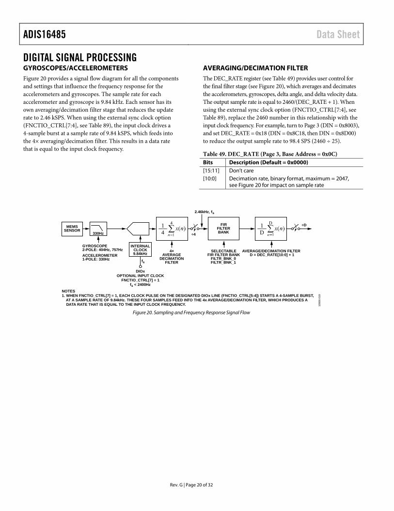
DIGITAL SIGNAL PROCESSING GYROSCOPES/ACCELEROMETERS Figure 20 provides a signal flow diagram for all the components and settings that influence the frequency response for the accelerometers and gyroscopes. The sample rate for each accelerometer and gyroscope is 9.84 kHz. Each sensor has its own averaging/decimation filter stage that reduces the update rate to 2.46 kSPS. When using the external sync clock option (FNCTIO_CTRL[7:4], see Table 89), the input clock drives a 4-sample burst at a sample rate of 9.84 kSPS, which feeds into the 4× averaging/decimation filter. This results in a data rate that is equal to the input clock frequency.
AVERAGING/DECIMATION FILTER The DEC_RATE register (see Table 49) provides user control for the final filter stage (see Figure 20), which averages and decimates the accelerometers, gyroscopes, delta angle, and delta velocity data. The output sample rate is equal to 2460/(DEC_RATE + 1). When using the external sync clock option (FNCTIO_CTRL[7:4], see Table 89), replace the 2460 number in this relationship with the input clock frequency. For example, turn to Page 3 (DIN = 0x8003), and set DEC_RATE = 0x18 (DIN = 0x8C18, then DIN = 0x8D00) to reduce the output sample rate to 98.4 SPS (2460 ÷ 25).
Table 49. DEC_RATE (Page 3, Base Address = 0x0C) Bits Description (Default = 0x0000) [15:11] Don’t care [10:0] Decimation rate, binary format, maximum = 2047,
see Figure 20 for impact on sample rate
MEMSSENSOR
330Hz ÷4
2.46kHz, fs
GYROSCOPE2-POLE: 404Hz, 757HzACCELEROMETER1-POLE: 330Hz
4×AVERAGE
DECIMATIONFILTER
SELECTABLEFIR FILTER BANK
FILTR_BNK_0FILTR_BNK_1
AVERAGE/DECIMATION FILTERD = DEC_RATE[10:0] + 1
14
4 ÷D1D
DFIRFILTERBANK
fs
INTERNALCLOCK9.84kHz
DIOxOPTIONAL INPUT CLOCK
FNCTIO_CTRL[7] = 1fs < 2400Hz
NOTES1. WHEN FNCTIO_CTRL[7] = 1, EACH CLOCK PULSE ON THE DESIGNATED DIOx LINE (FNCTIO_CTRL[5:4]) STARTS A 4-SAMPLE BURST,
AT A SAMPLE RATE OF 9.84kHz. THESE FOUR SAMPLES FEED INTO THE 4x AVERAGE/DECIMATION FILTER, WHICH PRODUCES ADATA RATE THAT IS EQUAL TO THE INPUT CLOCK FREQUENCY. 10
666-
019
Figure 20. Sampling and Frequency Response Signal Flow
Data Sheet ADIS16485
Rev. G | Page 21 of 32
FIR FILTER BANKS The ADIS16485 provides four configurable, 120-tap FIR filter banks. Each coefficient is 16 bits wide and occupies its own register location with each page. When designing a FIR filter for these banks, use a sample rate of 2.46 kHz and scale the coefficients so that their sum equals 32,768. For filter designs that have less than 120 taps, load the coefficients into the lower portion of the filter and start with Coefficient 1. Make sure that all unused taps are equal to zero, so that they do not add phase delay to the response. The FILTR_BNK_x registers provide three bits per sensor, which configure the filter bank (A, B, C, D) and turn filtering on and off. For example, turn to Page 3 (DIN = 0x8003), then write 0x002F to FILTR_BNK_0 (DIN = 0x962F, DIN = 0x9700) to set the x-axis gyroscope to use the FIR filter in Bank D, to set the y-axis gyroscope to use the FIR filter in Bank B, and to enable these FIR filters in both x- and y-axis gyroscopes. Note that the filter settings update after writing to the upper byte; therefore, always configure the lower byte first. In cases that require configuration to only the lower byte of either FILTR_BNK_0 or FILTR_BNK_1, complete the process by writing 0x00 to the upper byte.
Table 50. FILTR_BNK_0 (Page 3, Base Address = 0x16) Bits Description (Default = 0x0000) 15 Don’t care 14 Y-axis accelerometer filter enable (1 = enabled) [13:12] Y-axis accelerometer filter bank selection:
00 = Bank A, 01 = Bank B, 10 = Bank C, 11 = Bank D 11 X-axis accelerometer filter enable (1 = enabled) [10:9] X-axis accelerometer filter bank selection:
00 = Bank A, 01 = Bank B, 10 = Bank C, 11 = Bank D 8 Z-axis gyroscope filter enable (1 = enabled) [7:6] Z-axis gyroscope filter bank selection:
00 = Bank A, 01 = Bank B, 10 = Bank C, 11 = Bank D 5 Y-axis gyroscope filter enable (1 = enabled) [4:3] Y-axis gyroscope filter bank selection:
00 = Bank A, 01 = Bank B, 10 = Bank C, 11 = Bank D 2 X-axis gyroscope filter enable (1 = enabled) [1:0] X-axis gyroscope filter bank selection:
00 = Bank A, 01 = Bank B, 10 = Bank C, 11 = Bank D
Table 51. FILTR_BNK_1 (Page 3, Base Address = 0x18) Bits Description (Default = 0x0000) [15:3] Don’t care 2 Z-axis accelerometer filter enable (1 = enabled) [1:0] Z-axis accelerometer filter bank selection:
00 = Bank A, 01 = Bank B, 10 = Bank C, 11 = Bank D
Filter Memory Organization
Each filter bank uses two pages of the user register structure. See Table 52, Table 53, Table 54 and Table 55 for the register addresses in each filter bank.
Table 52. Filter Bank A Memory Map, FIR_COEF_Axxx Page PAGE_ID Address Register 5 0x05 0x00 PAGE_ID 5 0x05 0x02 to 0x07 Not used 5 0x05 0x08 FIR_COEF_A000 5 0x05 0x0A FIR_COEF_A001 5 0x05 0x0C to 0x7C FIR_COEF_A002 to
FIR_COEF_A058 5 0x05 0x7E FIR_COEF_A059 6 0x06 0x00 PAGE_ID 6 0x06 0x02 to 0x07 Not used 6 0x06 0x08 FIR_COEF_A060 6 0x06 0x0A FIR_COEF_A061 6 0x06 0x0C to 0x7C FIR_COEF_A062 to
FIR_COEF_A118 6 0x06 0x7E FIR_COEF_A119
Table 53. Filter Bank B Memory Map, FIR_COEF_Bxxx Page PAGE_ID Address Register 7 0x07 0x00 PAGE_ID 7 0x07 0x02 to 0x07 Not used 7 0x07 0x08 FIR_COEF_B000 7 0x07 0x0A FIR_COEF_B001 7 0x07 0x0C to 0x7C FIR_COEF_B002 to
FIR_COEF_B058 7 0x07 0x7E FIR_COEF_B059 8 0x08 0x00 PAGE_ID 8 0x08 0x02 to 0x07 Not used 8 0x08 0x08 FIR_COEF_B060 8 0x08 0x0A FIR_COEF_B061 8 0x08 0x0C to 0x7C FIR_COEF_B062 to
FIR_COEF_B118 8 0x08 0x7E FIR_COEF_B119
Table 54. Filter Bank C Memory Map, FIR_COEF_Cxxx Page PAGE_ID Address Register 9 0x09 0x00 PAGE_ID 9 0x09 0x02 to 0x07 Not used 9 0x09 0x08 FIR_COEF_C000 9 0x09 0x0A FIR_COEF_C001 9 0x09 0x0C to 0x7C FIR_COEF_C002 to
FIR_COEF_C058 9 0x09 0x7E FIR_COEF_C059 10 0x0A 0x00 PAGE_ID 10 0x0A 0x02 to 0x07 Not used 10 0x0A 0x08 FIR_COEF_C060 10 0x0A 0x0A FIR_COEF_C061 10 0x0A 0x0C to 0x7C FIR_COEF_C062 to
FIR_COEF_C118 10 0x0A 0x7E FIR_COEF_C119
ADIS16485 Data Sheet
Rev. G | Page 22 of 32
Table 55. Filter Bank D Memory Map, FIR_COEF_Dxxx Page PAGE_ID Address Register 11 0x0B 0x00 PAGE_ID 11 0x0B 0x02 to 0x07 Not used 11 0x0B 0x08 FIR_COEF_D000 11 0x0B 0x0A FIR_COEF_D001 11 0x0B 0x0C to 0x7C FIR_COEF_D002 to
FIR_COEF_D058 11 0x0B 0x7E FIR_COEF_D059 12 0x0C 0x00 PAGE_ID 12 0x0C 0x02 to 0x07 Not used 12 0x0C 0x08 FIR_COEF_D060 12 0x0C 0x0A FIR_COEF_D061 12 0x0C 0x0C to 0x7C FIR_COEF_D062 to
FIR_COEF_D118 12 0x0C 0x7E FIR_COEF_D119
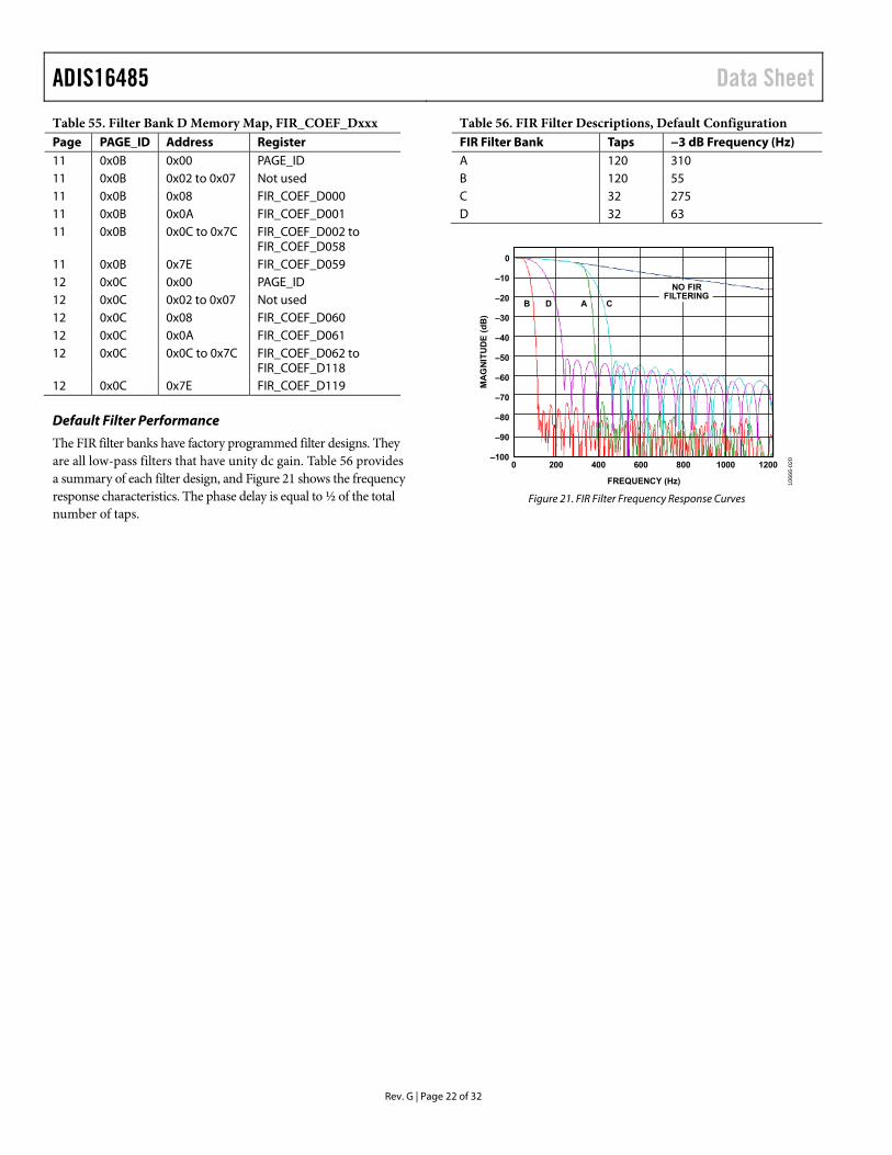
Default Filter Performance
The FIR filter banks have factory programmed filter designs. They are all low-pass filters that have unity dc gain. Table 56 provides a summary of each filter design, and Figure 21 shows the frequency response characteristics. The phase delay is equal to ½ of the total number of taps.
Table 56. FIR Filter Descriptions, Default Configuration FIR Filter Bank Taps −3 dB Frequency (Hz) A 120 310 B 120 55 C 32 275 D 32 63
NO FIRFILTERING
0
–10
–20
MA
GN
ITU
DE
(dB
) –30
–40
–50
–60
–70
–80
–90
–1000 200 400 600 800 1000 1200
FREQUENCY (Hz)
AD CB
1066
6-02
0
Figure 21. FIR Filter Frequency Response Curves
Data Sheet ADIS16485
Rev. G | Page 23 of 32
CALIBRATION The ADIS16485 factory calibration produces correction formulas for the gyroscopes and the accelerometers and then programs them into the flash memory. In addition, there are a series of user-configurable calibration registers for in-system tuning.
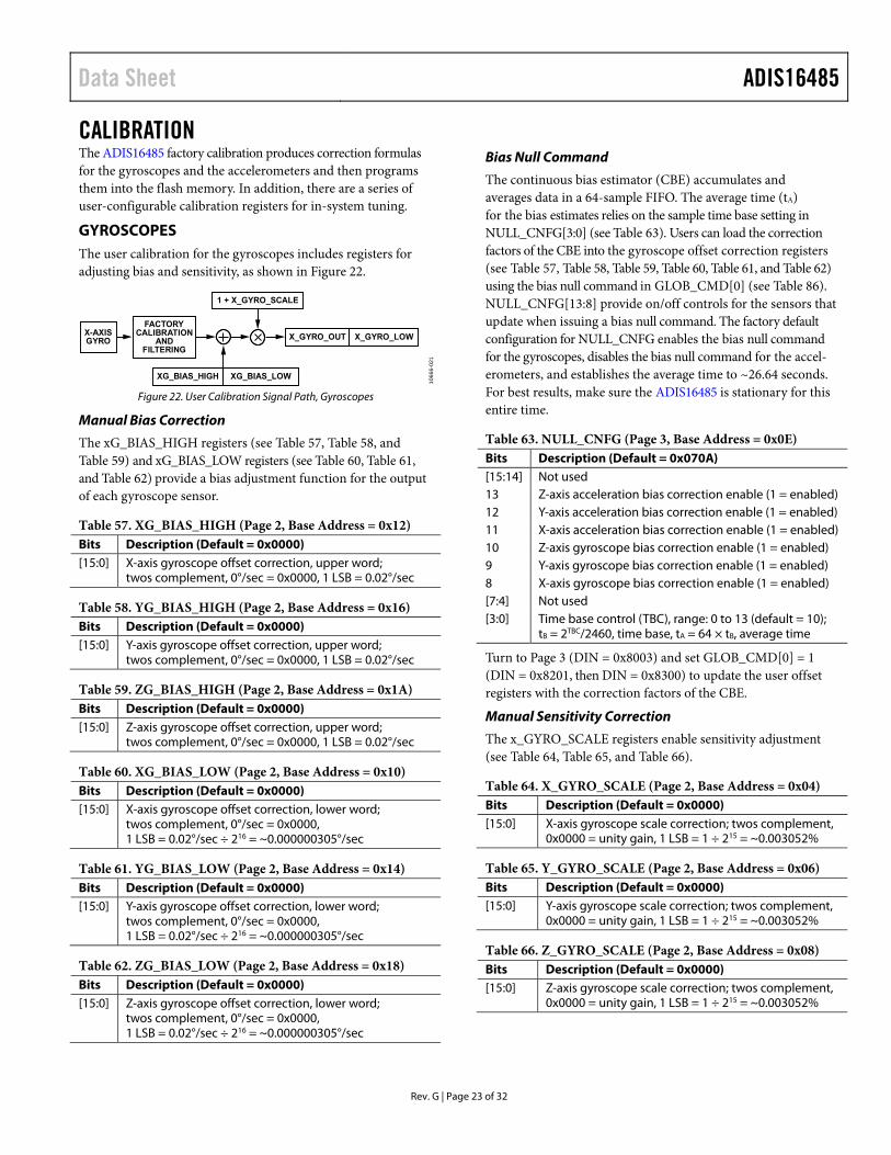
GYROSCOPES The user calibration for the gyroscopes includes registers for adjusting bias and sensitivity, as shown in Figure 22.
X-AXISGYRO
FACTORYCALIBRATION
ANDFILTERING
X_GYRO_OUT X_GYRO_LOW
XG_BIAS_HIGH XG_BIAS_LOW
1 + X_GYRO_SCALE
1066
6-02
1
Figure 22. User Calibration Signal Path, Gyroscopes
Manual Bias Correction
The xG_BIAS_HIGH registers (see Table 57, Table 58, and Table 59) and xG_BIAS_LOW registers (see Table 60, Table 61, and Table 62) provide a bias adjustment function for the output of each gyroscope sensor.
Table 57. XG_BIAS_HIGH (Page 2, Base Address = 0x12) Bits Description (Default = 0x0000) [15:0] X-axis gyroscope offset correction, upper word;
twos complement, 0°/sec = 0x0000, 1 LSB = 0.02°/sec
Table 58. YG_BIAS_HIGH (Page 2, Base Address = 0x16) Bits Description (Default = 0x0000) [15:0] Y-axis gyroscope offset correction, upper word;
twos complement, 0°/sec = 0x0000, 1 LSB = 0.02°/sec
Table 59. ZG_BIAS_HIGH (Page 2, Base Address = 0x1A) Bits Description (Default = 0x0000) [15:0] Z-axis gyroscope offset correction, upper word;
twos complement, 0°/sec = 0x0000, 1 LSB = 0.02°/sec
Table 60. XG_BIAS_LOW (Page 2, Base Address = 0x10) Bits Description (Default = 0x0000) [15:0] X-axis gyroscope offset correction, lower word;
twos complement, 0°/sec = 0x0000, 1 LSB = 0.02°/sec ÷ 216 = ~0.000000305°/sec
Table 61. YG_BIAS_LOW (Page 2, Base Address = 0x14) Bits Description (Default = 0x0000) [15:0] Y-axis gyroscope offset correction, lower word;
twos complement, 0°/sec = 0x0000, 1 LSB = 0.02°/sec ÷ 216 = ~0.000000305°/sec
Table 62. ZG_BIAS_LOW (Page 2, Base Address = 0x18) Bits Description (Default = 0x0000) [15:0] Z-axis gyroscope offset correction, lower word;
twos complement, 0°/sec = 0x0000, 1 LSB = 0.02°/sec ÷ 216 = ~0.000000305°/sec
Bias Null Command
The continuous bias estimator (CBE) accumulates and averages data in a 64-sample FIFO. The average time (tA) for the bias estimates relies on the sample time base setting in NULL_CNFG[3:0] (see Table 63). Users can load the correction factors of the CBE into the gyroscope offset correction registers (see Table 57, Table 58, Table 59, Table 60, Table 61, and Table 62) using the bias null command in GLOB_CMD[0] (see Table 86). NULL_CNFG[13:8] provide on/off controls for the sensors that update when issuing a bias null command. The factory default configuration for NULL_CNFG enables the bias null command for the gyroscopes, disables the bias null command for the accel-erometers, and establishes the average time to ~26.64 seconds. For best results, make sure the ADIS16485 is stationary for this entire time.
Table 63. NULL_CNFG (Page 3, Base Address = 0x0E) Bits Description (Default = 0x070A) [15:14] Not used 13 Z-axis acceleration bias correction enable (1 = enabled) 12 Y-axis acceleration bias correction enable (1 = enabled) 11 X-axis acceleration bias correction enable (1 = enabled) 10 Z-axis gyroscope bias correction enable (1 = enabled) 9 Y-axis gyroscope bias correction enable (1 = enabled) 8 X-axis gyroscope bias correction enable (1 = enabled) [7:4] Not used [3:0] Time base control (TBC), range: 0 to 13 (default = 10);
tB = 2TBC/2460, time base, tA = 64 × tB, average time
Turn to Page 3 (DIN = 0x8003) and set GLOB_CMD[0] = 1 (DIN = 0x8201, then DIN = 0x8300) to update the user offset registers with the correction factors of the CBE.
Manual Sensitivity Correction
The x_GYRO_SCALE registers enable sensitivity adjustment (see Table 64, Table 65, and Table 66).
Table 64. X_GYRO_SCALE (Page 2, Base Address = 0x04) Bits Description (Default = 0x0000) [15:0] X-axis gyroscope scale correction; twos complement,
0x0000 = unity gain, 1 LSB = 1 ÷ 215 = ~0.003052%
Table 65. Y_GYRO_SCALE (Page 2, Base Address = 0x06) Bits Description (Default = 0x0000) [15:0] Y-axis gyroscope scale correction; twos complement,
0x0000 = unity gain, 1 LSB = 1 ÷ 215 = ~0.003052%
Table 66. Z_GYRO_SCALE (Page 2, Base Address = 0x08) Bits Description (Default = 0x0000) [15:0] Z-axis gyroscope scale correction; twos complement,
0x0000 = unity gain, 1 LSB = 1 ÷ 215 = ~0.003052%
ADIS16485 Data Sheet
Rev. G | Page 24 of 32
Linear Acceleration on Effect on Gyroscope Bias
MEMS gyroscopes typically have a bias response to linear accel-eration that is normal to their axes of rotation. The ADIS16485 offers an optional compensation function for this effect; the factory default setting (0x00C0) for the CONFIG register enables this function. To turn it off, turn to Page 3 (DIN = 0x8003) and set CONFIG[7] = 0 (DIN = 0x8A20, DIN = 0x8B00). Note that this also keeps the point of percussion alignment function enabled.
Table 67. CONFIG (Page 3, Base Address = 0x0A) Bits Description (Default = 0x00C0) [15:8] Not used 7 Linear-g compensation for gyroscopes (1 = enabled) 6 Point of percussion alignment (1 = enabled) [5:2] Not used 1 Real-time clock, daylight savings time (1: enabled,
0: disabled) 0 Real-time clock control (1: relative/elapsed timer mode,
0: calendar mode)
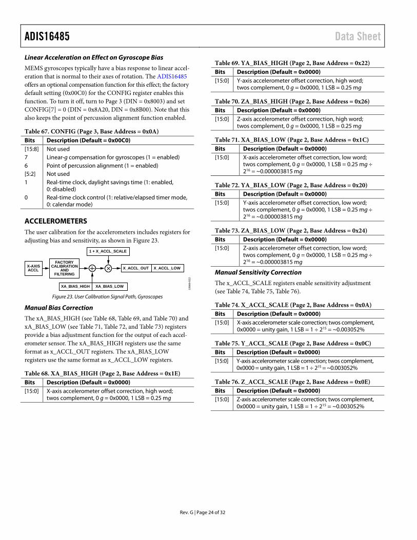
ACCELEROMETERS The user calibration for the accelerometers includes registers for adjusting bias and sensitivity, as shown in Figure 23.
X-AXISACCL
FACTORYCALIBRATION
ANDFILTERING
X_ACCL_OUT X_ACCL_LOW
XA_BIAS_HIGH XA_BIAS_LOW
1 + X_ACCL_SCALE
1066
6-02
2
Figure 23. User Calibration Signal Path, Gyroscopes
Manual Bias Correction
The xA_BIAS_HIGH (see Table 68, Table 69, and Table 70) and xA_BIAS_LOW (see Table 71, Table 72, and Table 73) registers provide a bias adjustment function for the output of each accel-erometer sensor. The xA_BIAS_HIGH registers use the same format as x_ACCL_OUT registers. The xA_BIAS_LOW registers use the same format as x_ACCL_LOW registers.
Table 68. XA_BIAS_HIGH (Page 2, Base Address = 0x1E) Bits Description (Default = 0x0000) [15:0] X-axis accelerometer offset correction, high word;
twos complement, 0 g = 0x0000, 1 LSB = 0.25 mg
Table 69. YA_BIAS_HIGH (Page 2, Base Address = 0x22) Bits Description (Default = 0x0000) [15:0] Y-axis accelerometer offset correction, high word;
twos complement, 0 g = 0x0000, 1 LSB = 0.25 mg
Table 70. ZA_BIAS_HIGH (Page 2, Base Address = 0x26) Bits Description (Default = 0x0000) [15:0] Z-axis accelerometer offset correction, high word;
twos complement, 0 g = 0x0000, 1 LSB = 0.25 mg
Table 71. XA_BIAS_LOW (Page 2, Base Address = 0x1C) Bits Description (Default = 0x0000) [15:0] X-axis accelerometer offset correction, low word;
twos complement, 0 g = 0x0000, 1 LSB = 0.25 mg ÷ 216 = ~0.000003815 mg
Table 72. YA_BIAS_LOW (Page 2, Base Address = 0x20) Bits Description (Default = 0x0000) [15:0] Y-axis accelerometer offset correction, low word;
twos complement, 0 g = 0x0000, 1 LSB = 0.25 mg ÷ 216 = ~0.000003815 mg
Table 73. ZA_BIAS_LOW (Page 2, Base Address = 0x24) Bits Description (Default = 0x0000) [15:0] Z-axis accelerometer offset correction, low word;
twos complement, 0 g = 0x0000, 1 LSB = 0.25 mg ÷ 216 = ~0.000003815 mg
Manual Sensitivity Correction
The x_ACCL_SCALE registers enable sensitivity adjustment (see Table 74, Table 75, Table 76).
Table 74. X_ACCL_SCALE (Page 2, Base Address = 0x0A) Bits Description (Default = 0x0000) [15:0] X-axis accelerometer scale correction; twos complement,
0x0000 = unity gain, 1 LSB = 1 ÷ 215 = ~0.003052%
Table 75. Y_ACCL_SCALE (Page 2, Base Address = 0x0C) Bits Description (Default = 0x0000) [15:0] Y-axis accelerometer scale correction; twos complement,
0x0000 = unity gain, 1 LSB = 1 ÷ 215 = ~0.003052%
Table 76. Z_ACCL_SCALE (Page 2, Base Address = 0x0E) Bits Description (Default = 0x0000) [15:0] Z-axis accelerometer scale correction; twos complement,
0x0000 = unity gain, 1 LSB = 1 ÷ 215 = ~0.003052%
Data Sheet ADIS16485
Rev. G | Page 25 of 32
RESTORING FACTORY CALIBRATION Turn to Page 3 (DIN = 0x8003) and set GLOB_CMD[6] = 1 (DIN = 0x8240, DIN = 0x8300) to execute the factory calibration restore function. This function resets each user calibration register to zero, resets all sensor data to 0, and automatically updates the flash memory within 900 ms. See Table 86 for more information on GLOB_CMD.
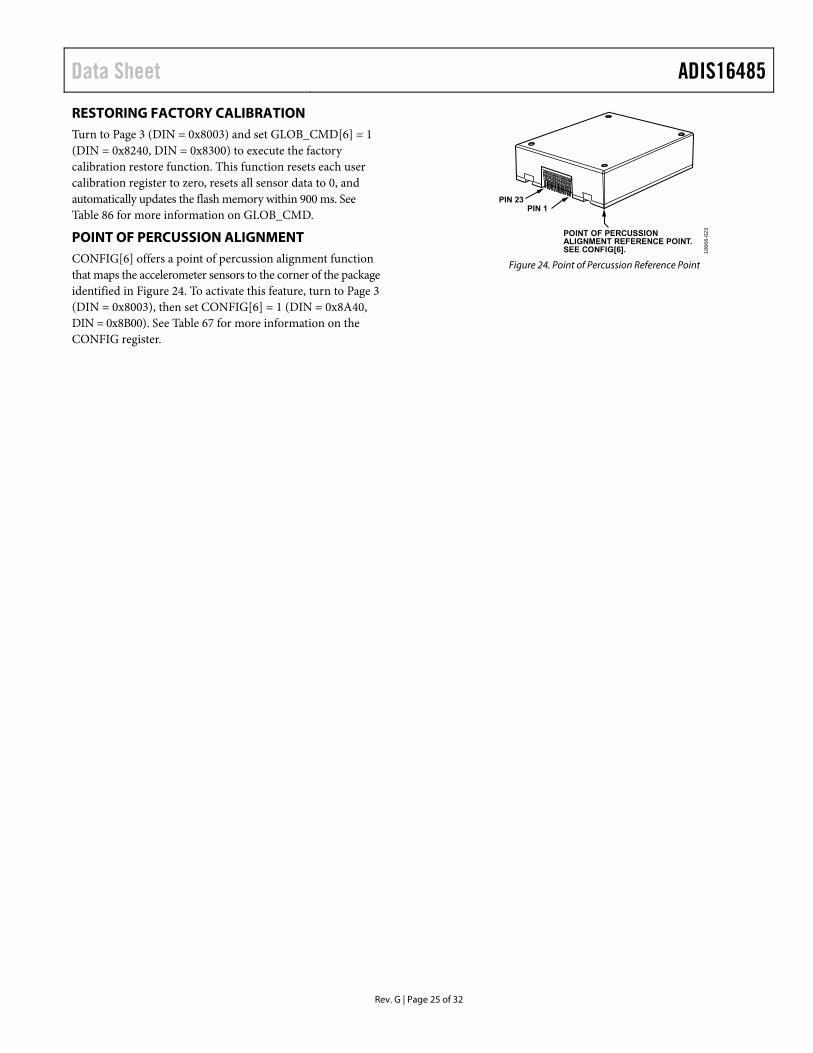
POINT OF PERCUSSION ALIGNMENT CONFIG[6] offers a point of percussion alignment function that maps the accelerometer sensors to the corner of the package identified in Figure 24. To activate this feature, turn to Page 3 (DIN = 0x8003), then set CONFIG[6] = 1 (DIN = 0x8A40, DIN = 0x8B00). See Table 67 for more information on the CONFIG register.
PIN 1PIN 23
POINT OF PERCUSSIONALIGNMENT REFERENCE POINT.SEE CONFIG[6]. 10
666-
023
Figure 24. Point of Percussion Reference Point
ADIS16485 Data Sheet
Rev. G | Page 26 of 32
ALARMS Each sensor has an independent alarm function that provides controls for alarm magnitude, polarity, and enabling a dynamic rate-of-change option. The ALM_STS register (see Table 43) contains the alarm output flags and the FNCTIO_CTRL register (see Table 89) provides an option for configuring one of the digital I/O lines as an alarm indicator.
STATIC ALARM USE The static alarm setting compares the output of each sensor with the trigger settings in the xx_ALM_MAGN registers (see Table 77, Table 78, Table 79, Table 80, Table 81, and Table 82) of that sensor. The polarity controls for each alarm are in the ALM_CNFG_x registers (see Table 83 and Table 84) and establish the relationship for the condition that causes the corresponding alarm flag to be active. For example, when ALM_CNFG_0[13] = 1, the alarm flag for the x-axis accelerometer (ALM_STS[3], see Table 43) becomes active (equal to 1) when X_ACCL_OUT is greater than XA_ALM_MAGN.
DYNAMIC ALARM USE The dynamic alarm setting provides the option to compare the change in each sensor output over a period of 48.7 ms with the xx_ALM_MAGN register that sensor.
Table 77. XG_ALM_MAGN (Page 3, Base Address = 0x28) Bits Description (Default = 0x0000) [15:0] X-axis gyroscope alarm threshold settings;
twos complement, 0°/sec = 0x0000, 1 LSB = 0.02°/sec
Table 78. YG_ALM_MAGN (Page 3, Base Address = 0x2A) Bits Description (Default = 0x0000) [15:0] Y-axis gyroscope alarm threshold settings;
twos complement, 0°/sec = 0x0000, 1 LSB = 0.02°/sec
Table 79. ZG_ALM_MAGN (Page 3, Base Address = 0x2C) Bits Description (Default = 0x0000) [15:0] Z-axis gyroscope alarm threshold settings;
twos complement, 0°/sec = 0x0000, 1 LSB = 0.02°/sec
Table 80. XA_ALM_MAGN (Page 3, Base Address = 0x2E) Bits Description (Default = 0x0000) [15:0] X-axis accelerometer alarm threshold settings;
twos complement, 0 g = 0x0000, 1 LSB = 0.25 mg
Table 81. YA_ALM_MAGN (Page 3, Base Address = 0x30) Bits Description (Default = 0x0000) [15:0] Y-axis accelerometer alarm threshold settings;
twos complement, 0 g = 0x0000, 1 LSB = 0.25 mg
Table 82. ZA_ALM_MAGN (Page 3, Base Address = 0x32) Bits Description (Default = 0x0000) [15:0] Z-axis accelerometer alarm threshold settings;
twos complement, 0 g = 0x0000, 1 LSB = 0.25 mg
Table 83. ALM_CNFG_0 (Page 3, Base Address = 0x20) Bits Description (Default = 0x0000) 15 X-axis accelerometer alarm (1 = enabled) 14 Not used 13 X-axis accelerometer alarm polarity 1 = active when X_ACCL_OUT > XA_ALM_MAGN 0 = active when X_ACCL_OUT > XA_ALM_MAGN 12 X-axis accelerometer dynamic enable (1 = enabled) 11 Z-axis gyroscope alarm (1 = enabled) 10 Not used 9 Z-axis gyroscope alarm polarity 1 = active when Z_GYRO_OUT > ZG_ALM_MAGN 0 = active when Z_GYRO_OUT > ZG_ALM_MAGN 8 Z-axis gyroscope dynamic enable (1 = enabled) 7 Y-axis gyroscope alarm (1 = enabled) 6 Not used 5 Y-axis gyroscope alarm polarity 1 = active when Y_GYRO_OUT > YG_ALM_MAGN 0 = active when Y_GYRO_OUT > YG_ALM_MAGN 4 Y-axis gyroscope dynamic enable (1 = enabled) 3 X-axis gyroscope alarm (1 = enabled) 2 Not used 1 X-axis gyroscope alarm polarity 1 = active when X_GYRO_OUT > XG_ALM_MAGN 0 = active when X_GYRO_OUT > XG_ALM_MAGN 0 X-axis gyroscope dynamic enable (1 = enabled)
Table 84. ALM_CNFG_1 (Page 3, Base Address = 0x22) Bits Description (Default = 0x0000) [15:8] Don’t care 7 Z-axis accelerometer alarm (1 = enabled) 6 Not used 5 Z-axis accelerometer alarm polarity 1 = active when Z_ACCL_OUT > ZA_ALM_MAGN 0 = active when Z_ACCL_OUT > ZA_ALM_MAGN 4 Z-axis accelerometer dynamic enable (1 = enabled) 3 Y-axis accelerometer alarm (1 = enabled) 2 Not used 1 Y-axis accelerometer alarm polarity 1 = active when Y_ACCL_OUT > YA_ALM_MAGN 0 = active when Y_ACCL_OUT > YA_ALM_MAGN 0 Y-axis accelerometer dynamic enable (1 = enabled)
Alarm Example
Table 85 offers an alarm configuration example, which sets the z-axis gyroscope alarm to trip when Z_GYRO_OUT > 131.1°/sec (0x199B).
Table 85. Alarm Configuration Example DIN Description 0xAC9B, 0xAD19 Set ZG_ALM_MAGN = 0x199B
0xA000, 0xA10A Set ALM_CNFG_0 = 0x0A00
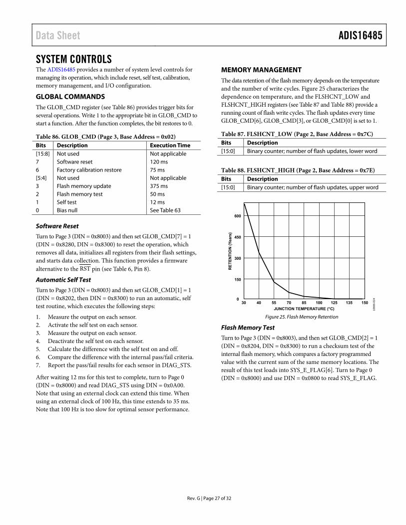
Data Sheet ADIS16485
Rev. G | Page 27 of 32
SYSTEM CONTROLS The ADIS16485 provides a number of system level controls for managing its operation, which include reset, self test, calibration, memory management, and I/O configuration.
GLOBAL COMMANDS The GLOB_CMD register (see Table 86) provides trigger bits for several operations. Write 1 to the appropriate bit in GLOB_CMD to start a function. After the function completes, the bit restores to 0.
Table 86. GLOB_CMD (Page 3, Base Address = 0x02) Bits Description Execution Time [15:8] Not used Not applicable 7 Software reset 120 ms 6 Factory calibration restore 75 ms [5:4] Not used Not applicable 3 Flash memory update 375 ms 2 Flash memory test 50 ms 1 Self test 12 ms 0 Bias null See Table 63
Software Reset
Turn to Page 3 (DIN = 0x8003) and then set GLOB_CMD[7] = 1 (DIN = 0x8280, DIN = 0x8300) to reset the operation, which removes all data, initializes all registers from their flash settings, and starts data collection. This function provides a firmware alternative to the A
RST E
A pin (see Table 6, Pin 8).
Automatic Self Test
Turn to Page 3 (DIN = 0x8003) and then set GLOB_CMD[1] = 1 (DIN = 0x8202, then DIN = 0x8300) to run an automatic, self test routine, which executes the following steps:
1. Measure the output on each sensor. 2. Activate the self test on each sensor. 3. Measure the output on each sensor. 4. Deactivate the self test on each sensor. 5. Calculate the difference with the self test on and off. 6. Compare the difference with the internal pass/fail criteria. 7. Report the pass/fail results for each sensor in DIAG_STS.
After waiting 12 ms for this test to complete, turn to Page 0 (DIN = 0x8000) and read DIAG_STS using DIN = 0x0A00. Note that using an external clock can extend this time. When using an external clock of 100 Hz, this time extends to 35 ms. Note that 100 Hz is too slow for optimal sensor performance.
MEMORY MANAGEMENT The data retention of the flash memory depends on the temperature and the number of write cycles. Figure 25 characterizes the dependence on temperature, and the FLSHCNT_LOW and FLSHCNT_HIGH registers (see Table 87 and Table 88) provide a running count of flash write cycles. The flash updates every time GLOB_CMD[6], GLOB_CMD[3], or GLOB_CMD[0] is set to 1.
Table 87. FLSHCNT_LOW (Page 2, Base Address = 0x7C) Bits Description [15:0] Binary counter; number of flash updates, lower word
Table 88. FLSHCNT_HIGH (Page 2, Base Address = 0x7E) Bits Description [15:0] Binary counter; number of flash updates, upper word
600
450
300
150
030 40
RE
TE
NT
ION
(Yea
rs)
JUNCTION TEMPERATURE (°C)
55 70 85 100 125 135 150
1066
6-02
4
Figure 25. Flash Memory Retention
Flash Memory Test
Turn to Page 3 (DIN = 0x8003), and then set GLOB_CMD[2] = 1 (DIN = 0x8204, DIN = 0x8300) to run a checksum test of the internal flash memory, which compares a factory programmed value with the current sum of the same memory locations. The result of this test loads into SYS_E_FLAG[6]. Turn to Page 0 (DIN = 0x8000) and use DIN = 0x0800 to read SYS_E_FLAG.
ADIS16485 Data Sheet
Rev. G | Page 28 of 32
GENERAL-PURPOSE I/O There are four general-purpose I/O pins: DIO1, DIO2, DIO3, and DIO4. The FNCTIO_CTRL register controls the basic function of each I/O pin. Each I/O pin only supports one function at a time. In cases where a single pin has two different assignments, the enable bit for the lower priority function automatically resets to zero and is disabled. The priority is (1) data-ready, (2) sync clock input, (3) alarm indicator, and (4) general-purpose, where 1 identifies the highest priority and 4 indicates the lowest priority.
Table 89. FNCTIO_CTRL (Page 3, Base Address = 0x06) Bits Description (Default = 0x000D) [15:12] Not used 11 Alarm indicator: 1 = enabled, 0 = disabled 10 Alarm indicator polarity: 1 = positive, 0 = negative [9:8] Alarm indicator line selection:
00 = DIO1, 01 = DIO2, 10 = DIO3, 11 = DIO4 7 Sync clock input enable: 1 = enabled, 0 = disabled 6 Sync clock input polarity: 1 = rising edge, 0 = falling edge [5:4] Sync clock input line selection:
00 = DIO1, 01 = DIO2, 10 = DIO3, 11 = DIO4 3 Data-ready enable: 1 = enabled, 0 = disabled 2 Data-ready polarity: 1 = positive, 0 = negative [1:0] Data-ready line selection:
00 = DIO1, 01 = DIO2, 10 = DIO3, 11 = DIO4
Data-Ready Indicator
FNCTIO_CTRL[3:0] provide some configuration options for using one of the DIOx lines as a data-ready indicator signal, which can drive the interrupt control line of a processor. The factory default assigns DIO2 as a positive polarity, data-ready signal. Use the following sequence to change this assignment to DIO1 with a negative polarity: turn to Page 3 (DIN = 0x8003) and set FNCTIO_CTRL[3:0] = 1000 (DIN = 0x8608, then DIN = 0x8700). The timing jitter on the data-ready signal is ±1.4 µs.
Input Sync/Clock Control
FNCTIO_CTRL[7:4] provide some configuration options for using one of the DIOx lines as an input synchronization signal for sampling inertial sensor data. For example, use the following sequence to establish DIO4 as a positive polarity, input clock pin and keep the factory default setting for the data-ready function: turn to Page 3 (DIN = 0x8003) and set FNCTIO_CTRL[7:0] = 0xFD (DIN = 0x86FD, then DIN = 0x8700). Note that this command also disables the internal sampling clock, and no data sampling takes place without the input clock signal. When selecting a clock input frequency, consider the 330 Hz sensor bandwidth, because under sampling the sensors can degrade noise and stability performance.
General-Purpose I/O Control
When FNCTIO_CTRL does not configure a DIOx pin, GPIO_CTRL provides register controls for general-purpose use of the pin. GPIO_CTRL[3:0] provides input/output assignment controls for each pin. When the DIOx pins are inputs, monitor their levels by reading GPIO_CTRL[7:4]. When the DIOx pins are used as outputs, set their levels by writing to GPIO_CTRL[7:4]. For example, use the following sequence to set DIO1 and DIO3 as high and low output pins, respectively, and set DIO2 and DIO4 as input pins. Turn to Page 3 (DIN = 0x8003) and set GPIO_CTRL[7:0] = 0x15 (DIN = 0x8815, then DIN = 0x8900).
Table 90. GPIO_CTRL (Page 3, Base Address = 0x08) Bits Description (Default = 0x00X0)1 [15:8] Don’t care 7 General-Purpose I/O Line 4 (DIO4) data level 6 General-Purpose I/O Line 3 (DIO3) data level 5 General-Purpose I/O Line 2 (DIO2) data level 4 General-Purpose I/O Line 1 (DIO1) data level 3 General-Purpose I/O Line 4 (DIO4) direction control
(1 = output, 0 = input) 2 General-Purpose I/O Line 3 (DIO3) direction control
(1 = output, 0 = input) 1 General-Purpose I/O Line 2 (DIO2) direction control
(1 = output, 0 = input) 0 General-Purpose I/O Line 1 (DIO1) direction control
(1 = output, 0 = input) 1 The GPIO_CTRL register, Bits[7:4], reflect the levels on the DIOx pins and do
not have a default setting.
POWER MANAGEMENT The SLP_CNT register (see Table 91) provides controls for both power-down mode and sleep mode. The trade-off between power-down mode and sleep mode is between idle power and recovery time. Power-down mode offers the best idle power consumption but requires the most time to recover. Also, all volatile settings are lost during power-down but are preserved during sleep mode.
For timed sleep mode, turn to Page 3 (DIN = 0x8003), write the amount of sleep time to SLP_CNT[7:0] and then, set SLP_CNT[8] = 1 (DIN = 0x9101) to start the sleep period. For a timed power-down period, change the last command to set SLP_CNT[9] = 1 (DIN = 0x9102). To power down or sleep for an indefinite period, set SLP_CNT[7:0] = 0x00 first, then set either SLP_CNT[8] or SLP_CNT[9] to 1. Note that the command takes effect when the AA
CSEE
AA line goes high. To awaken the device from sleep or power-down mode, use one of the following options to restore normal operation:
• Assert AA
CSEE
AA from high to low. • Pulse AA
RST EE
AA low, then high again. • Cycle the power.
For example, set SLP_CNT[7:0] = 0x64 (DIN = 0x9064), then set SLP_CNT[8] = 1 (DIN = 0x9101) to start a sleep period of 100 seconds.
Data Sheet ADIS16485
Rev. G | Page 29 of 32
Table 91. SLP_CNT (Page 3, Base Address = 0x10) Bits Description [15:10] Not used 9 Power-down mode 8 Normal sleep mode [7:0] Programmable time bits; 1 sec/LSB; 0x00 = indefinite
If the sleep mode and power-down mode bits are both set high, the normal sleep mode (SLP_CNT[8]) bit takes precedence.
General-Purpose Registers
The USER_SCR_x registers (see Table 92, Table 93, Table 94, and Table 95) provide four 16-bit registers for storing data.
Table 92. USER_SCR_1 (Page 2, Base Address = 0x74) Bits Description [15:0] User-defined
Table 93. USER_SCR_2 (Page 2, Base Address = 0x76) Bits Description [15:0] User-defined
Table 94. USER_SCR_3 (Page 2, Base Address = 0x78) Bits Description [15:0] User-defined
Table 95. USER_SCR_4 (Page 2, Base Address = 0x7A) Bits Description [15:0] User-defined
Real-Time Clock Configuration/Data
The VDDRTC power supply pin (see Table 6, Pin 23) provides a separate supply for the real-time clock (RTC) function. This enables the RTC to keep track of time, even when the main supply (VDD) is off. Configure the RTC function by selecting one of two modes in CONFIG[0] (see Table 67). The real-time clock data is available in the TIME_MS_OUT register (see Table 96), TIME_DH_OUT register (see Table 97), and TIME_YM_OUT register (see Table 98). When using the elapsed timer mode, the time data registers start at 0x0000 when the device starts up (or resets) and begin keeping time in a manner that is similar to a stopwatch. When using the clock/calendar mode, write the current time to the real-time registers in the following sequence: seconds (TIME_MS_OUT[5:0]), minutes (TIME_ MS_OUT[13:8]), hours (TIME_DH_OUT[5:0]), day (TIME_DH_OUT[12:8]), month (TIME_YM_OUT[3:0]), and year (TIME_YM_OUT[14:8]).
The updates to the timer do not become active until there is a successful write to the TIME_ YM_OUT[14:8] byte. The real-time clock registers reflect the newly updated values only after the next seconds tick of the clock that follows the write to TIME_YM_OUT[14:8] (year). Writing to TIME_YM_OUT[14:8] activates all timing values; therefore, always write to this location last when updating the timer, even if the year information does not require updating.
Write the current time to each time data register after setting CONFIG[0] = 1 (DIN = 0x8003, DIN = 0x8A01). Note that CONFIG[1] provides a bit for managing daylight savings time. After the CONFIG and TIME_xx_OUT registers are configured, set GLOB_CMD[3] = 1 (DIN = 0x8003, DIN = 0x8208, DIN = 0x8300) to back up these settings up in flash, and use a separate 3.3 V source to supply power to the VDDRTC function. Note that access to time data in the TIME_xx_OUT registers requires normal operation (VDD = 3.3 V and full startup), but the timer function only requires that VDDRTC = 3.3 V when the rest of the ADIS16485 is turned off.
Table 96. TIME_MS_OUT (Page 0, Base Address = 0x78) Bits Description [15:14] Not used [13:8] Minutes, binary data, range = 0 to 59 [7:6] Not used [5:0] Seconds, binary data, range = 0 to 59
Table 97. TIME_DH_OUT (Page 0, Base Address = 0x7A) Bits Description [15:13] Not used [12:8] Day, binary data, range = 1 to 31 [7:6] Not used [5:0] Hours, binary data, range = 0 to 23
Table 98. TIME_YM_OUT (Page 0, Base Address = 0x7C) Bits Description [15] Not used [14:8] Year, binary data, range = 0 to 99, relative to 2000 A.D. [7:4] Not used [3:0] Month, binary data, range = 1 to 12
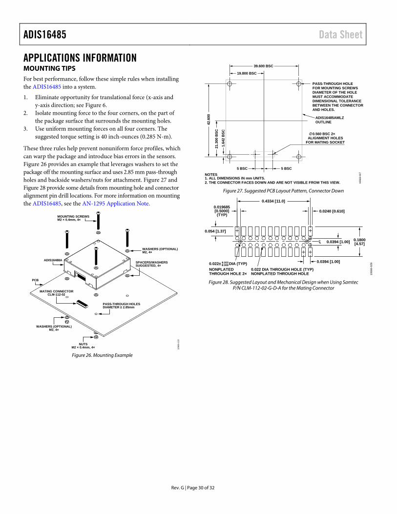
ADIS16485 Data Sheet
Rev. G | Page 30 of 32
APPLICATIONS INFORMATION MOUNTING TIPS For best performance, follow these simple rules when installing the ADIS16485 into a system.
1. Eliminate opportunity for translational force (x-axis and y-axis direction; see Figure 6.
2. Isolate mounting force to the four corners, on the part of the package surface that surrounds the mounting holes.
3. Use uniform mounting forces on all four corners. The suggested torque setting is 40 inch-ounces (0.285 N-m).
These three rules help prevent nonuniform force profiles, which can warp the package and introduce bias errors in the sensors. Figure 26 provides an example that leverages washers to set the package off the mounting surface and uses 2.85 mm pass-through holes and backside washers/nuts for attachment. Figure 27 and Figure 28 provide some details from mounting hole and connector alignment pin drill locations. For more information on mounting the ADIS16485, see the AN-1295 Application Note.
MOUNTING SCREWSM2 × 0.4mm, 4×
WASHERS (OPTIONAL)M2, 4×
ADIS16488A
WASHERS (OPTIONAL)M2, 4×
NUTSM2 × 0.4mm, 4×
MATING CONNECTORCLM-112-02
PCB
PASS-THROUGH HOLESDIAMETER ≥ 2.85mm
SPACERS/WASHERSSUGGESTED, 4×
1066
6-13
3
Figure 26. Mounting Example
0.560 BSC 2×ALIGNMENT HOLES
FOR MATING SOCKET
PASS-THROUGH HOLEFOR MOUNTING SCREWSDIAMETER OF THE HOLEMUST ACCOMMODATEDIMENSIONAL TOLERANCEBETWEEN THE CONNECTORAND HOLES.
19.800 BSC
39.600 BSC
42.6
00
21.3
00B
SC
5 BSC5 BSC
1.64
2B
SC
NOTES1. ALL DIMENSIONS IN mm UNITS.2. THE CONNECTOR FACES DOWN AND ARE NOT VISIBLE FROM THIS VIEW. 10
666-
027
ADIS16485AMLZOUTLINE
Figure 27. Suggested PCB Layout Pattern, Connector Down
0.4334 [11.0]
0.0240 [0.610]0.019685[0.5000](TYP)
0.054 [1.37]
0.0394 [1.00]
0.0394 [1.00] 0.1800[4.57]
NONPLATEDTHROUGH HOLE 2×
0.022± DIA (TYP)0.022 DIA THROUGH HOLE (TYP)NONPLATED THROUGH HOLE 10
666-
028
Figure 28. Suggested Layout and Mechanical Design when Using Samtec
P/N CLM-112-02-G-D-A for the Mating Connector
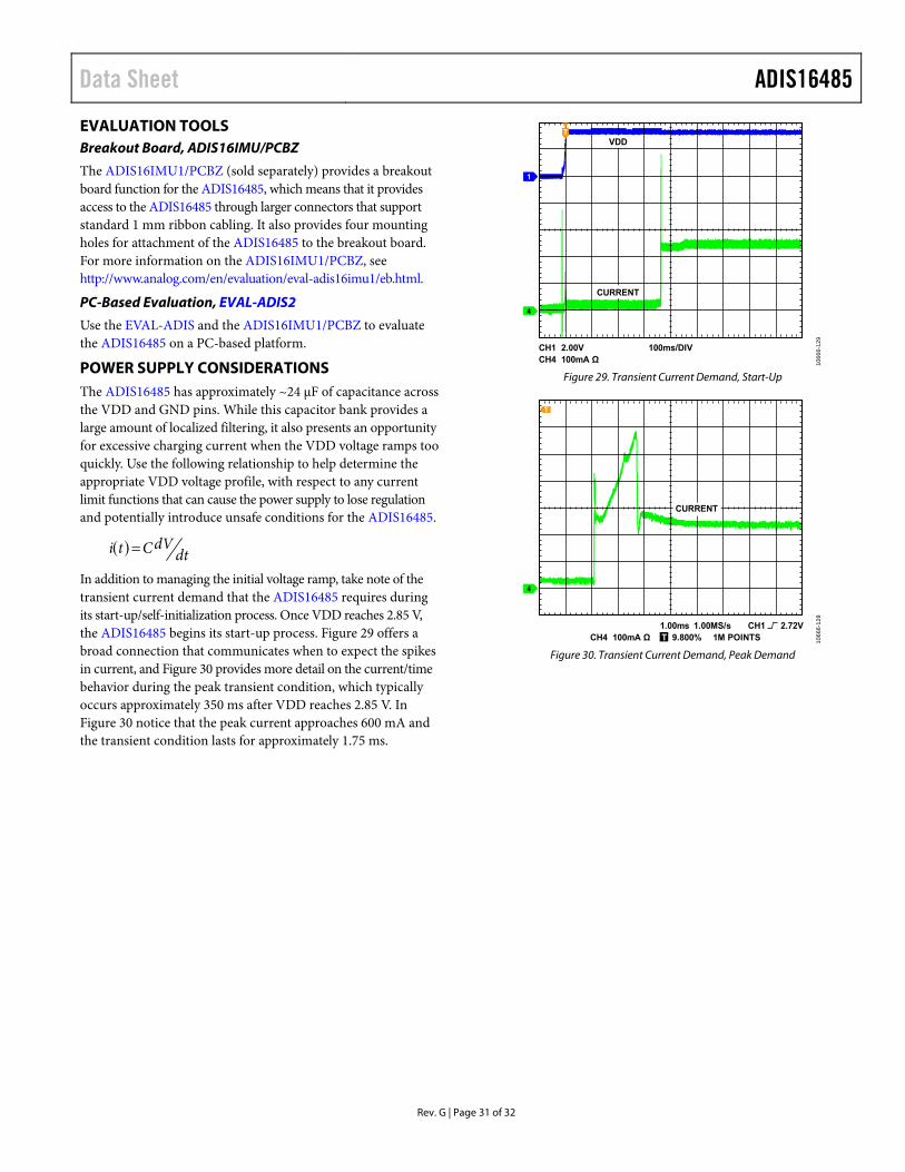
Data Sheet ADIS16485
Rev. G | Page 31 of 32
EVALUATION TOOLS Breakout Board, ADIS16IMU/PCBZ
The ADIS16IMU1/PCBZ (sold separately) provides a breakout board function for the ADIS16485, which means that it provides access to the ADIS16485 through larger connectors that support standard 1 mm ribbon cabling. It also provides four mounting holes for attachment of the ADIS16485 to the breakout board. For more information on the ADIS16IMU1/PCBZ, see http://www.analog.com/en/evaluation/eval-adis16imu1/eb.html.
PC-Based Evaluation, EVAL-ADIS2
Use the EVAL-ADIS and the ADIS16IMU1/PCBZ to evaluate the ADIS16485 on a PC-based platform.
POWER SUPPLY CONSIDERATIONS The ADIS16485 has approximately ~24 μF of capacitance across the VDD and GND pins. While this capacitor bank provides a large amount of localized filtering, it also presents an opportunity for excessive charging current when the VDD voltage ramps too quickly. Use the following relationship to help determine the appropriate VDD voltage profile, with respect to any current limit functions that can cause the power supply to lose regulation and potentially introduce unsafe conditions for the ADIS16485.
dtdVCti
In addition to managing the initial voltage ramp, take note of the transient current demand that the ADIS16485 requires during its start-up/self-initialization process. Once VDD reaches 2.85 V, the ADIS16485 begins its start-up process. Figure 29 offers a broad connection that communicates when to expect the spikes in current, and Figure 30 provides more detail on the current/time behavior during the peak transient condition, which typically occurs approximately 350 ms after VDD reaches 2.85 V. In Figure 30 notice that the peak current approaches 600 mA and the transient condition lasts for approximately 1.75 ms.
1066
6-12
9
CH1 2.00VCH4 100mA Ω
100ms/DIV
1
4
TVDD
CURRENT
Figure 29. Transient Current Demand, Start-Up
1066
6-12
8
CH4 100mA Ω 1M POINTS1.00ms 1.00MS/s CH1 2.72VT 9.800%
4
T
CURRENT
Figure 30. Transient Current Demand, Peak Demand
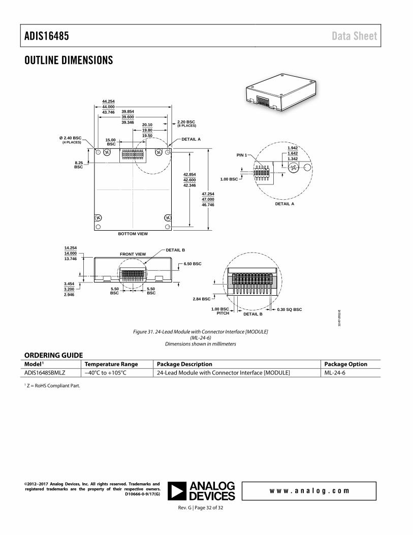
ADIS16485 Data Sheet
Rev. G | Page 32 of 32
OUTLINE DIMENSIONS
12-0
7-20
12-E
BOTTOM VIEW
FRONT VIEW
44.25444.00043.746
42.85442.60042.346
1.9421.6421.342
47.25447.00046.746
14.25414.00013.746
39.85439.60039.346 20.10
19.8019.50Ø 2.40 BSC
(4 PLACES) 15.00BSC
8.25BSC
2.20 BSC(8 PLACES)
DETAIL A
PIN 1
DETAIL B
5.50BSC
5.50BSC
1.00 BSC
2.84 BSC
6.50 BSC
DETAIL A
DETAIL B1.00 BSC
PITCH0.30 SQ BSC
3.4543.2002.946
Figure 31. 24-Lead Module with Connector Interface [MODULE]
(ML-24-6) Dimensions shown in millimeters
ORDERING GUIDE Model 13F
1 Temperature Range Package Description Package Option ADIS16485BMLZ −40°C to +105°C 24-Lead Module with Connector Interface [MODULE] ML-24-6 1 Z = RoHS Compliant Part.
©2012−2017 Analog Devices, Inc. All rights reserved. Trademarks and registered trademarks are the property of their respective owners. D10666-0-9/17(G)