Embed Size (px)
Citation preview
Taming light with plasmons –Taming light with plasmons –theory and experimentstheory and experiments
Aliaksandr Rahachou, ITN, LiU Aliaksandr Rahachou, ITN, LiU Kristofer Tvingstedt, IFM, LiUKristofer Tvingstedt, IFM, LiU
2006.10.19, Hjo
OUTLINEOUTLINE
• Introduction to plasmonics
• Optical excitation of plasmons
• Plasmons in organic solar cells
• Experimental results for APFO3:PCBM on Al gratings
• Theoretical results for APFO3:PCBM on Al gratings
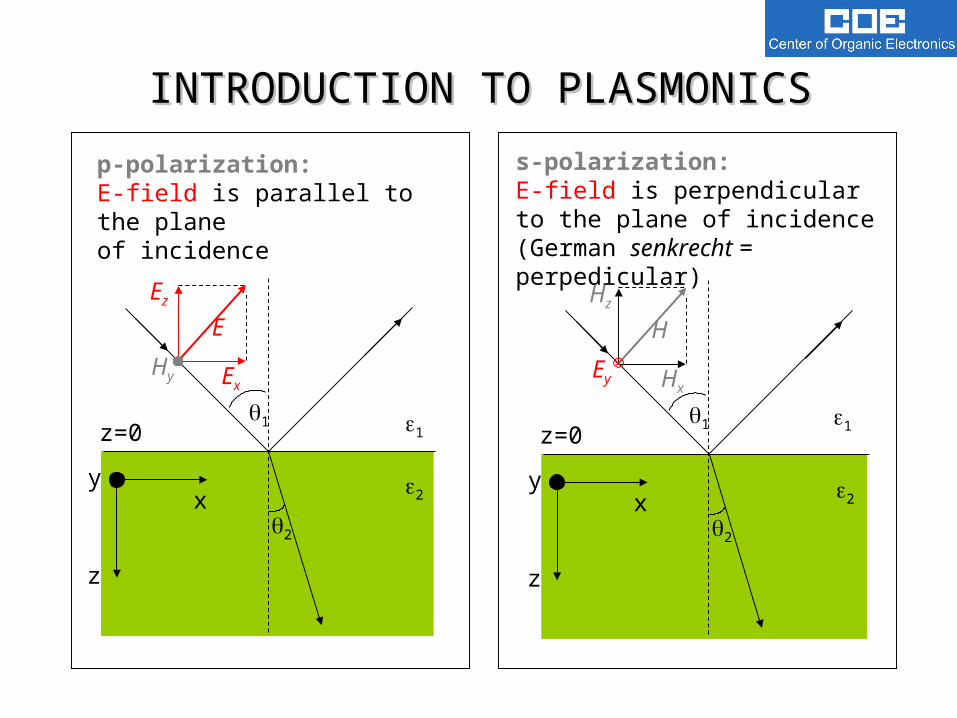
p-polarization: E-field is parallel to the plane of incidence
s-polarization: E-field is perpendicular to the plane of incidence (German senkrecht = perpedicular)
x
z
y
1
Hx
2
z=01
2
Ey
H
Hz
x
z
y
1
Ex
Ez
2
z=0 1
2
Hy
E
INTRODUCTION TO PLASMONICSINTRODUCTION TO PLASMONICS
x
z
y
z=0 1
2
E1x
E1z
H1y
E1
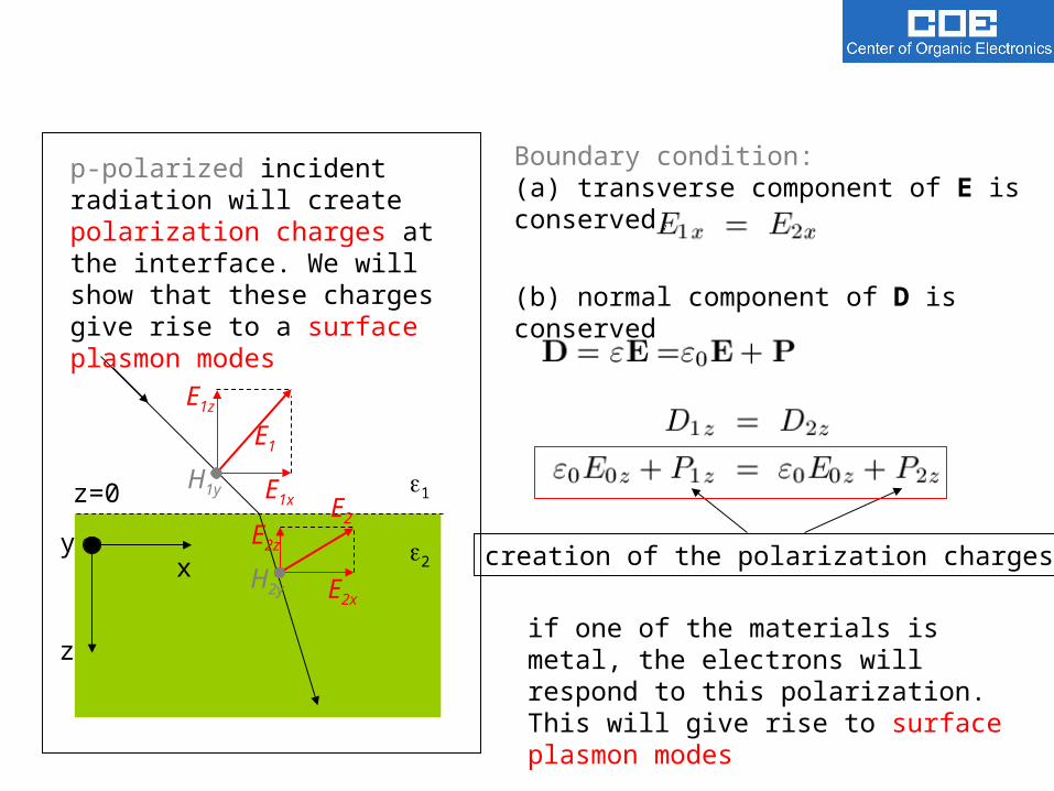
p-polarized incident radiation will create polarization charges at the interface. We will show that these charges give rise to a surface plasmon modes
E2x
E2z
H2y
E2
creation of the polarization charges
if one of the materials is metal, the electrons will respond to this polarization. This will give rise to surface plasmon modes
Boundary condition:(a) transverse component of E is conserved,
(b) normal component of D is conserved
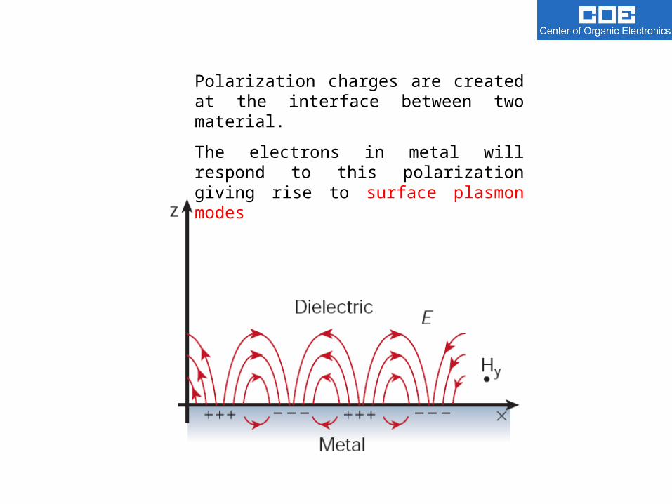
Polarization charges are created at the interface between two material.
The electrons in metal will respond to this polarization giving rise to surface plasmon modes
x
z
y
z=0 1
2
H1x
H1z
E1y
H1
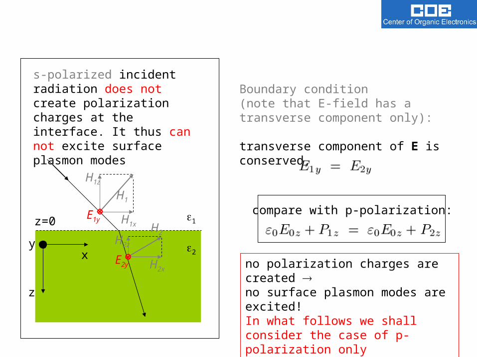
s-polarized incident radiation does not create polarization charges at the interface. It thus can not excite surface plasmon modes
H2x
H2z
E2y
H2
no polarization charges are created no surface plasmon modes are excited!In what follows we shall consider the case of p-polarization only
Boundary condition(note that E-field has a transverse component only):
transverse component of E is conserved,
compare with p-polarization:
More detailed theory
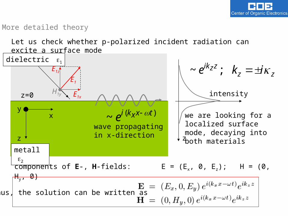
Let us check whether p-polarized incident radiation can excite a surface mode
x
z
y
z=0
dielectric1
metall 2
E1x
E1z
H1y
E1
)(~ txxkie
wave propagating in x-direction
intensity
z
zzzzik ike ;~
we are looking for a localized surface mode, decaying into both materials
components of E-, H-fields: E = (Ex, 0, Ez); H = (0, Hy, 0)
Thus, the solution can be written as
x
z
y
z=0
dielectric1
metall 2
E1x
E1z
H1y
E1
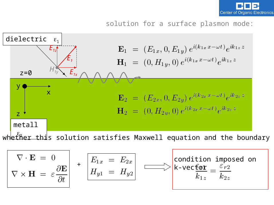
solution for a surface plasmon mode:
Let us see whether this solution satisfies Maxwell equation and the boundary conditions:
+condition imposed on k-vector
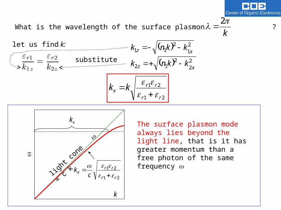
What is the wavelength of the surface plasmon ?k
2
let us find k: 2
22
12
21
211
xz
xz
kknk
kknk
substitute
21
21
rr
rrx kk
k
kx
21
21
rr
rrx ck
lig
ht co
ne =
c
k
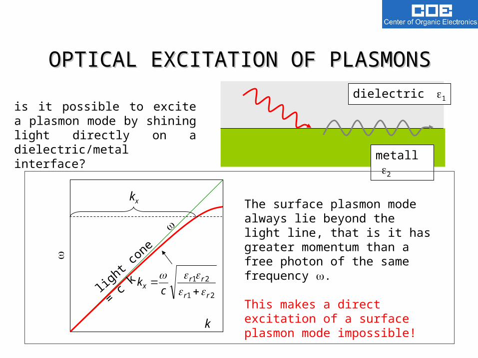
The surface plasmon mode always lies beyond the light line, that is it has greater momentum than a free photon of the same frequency
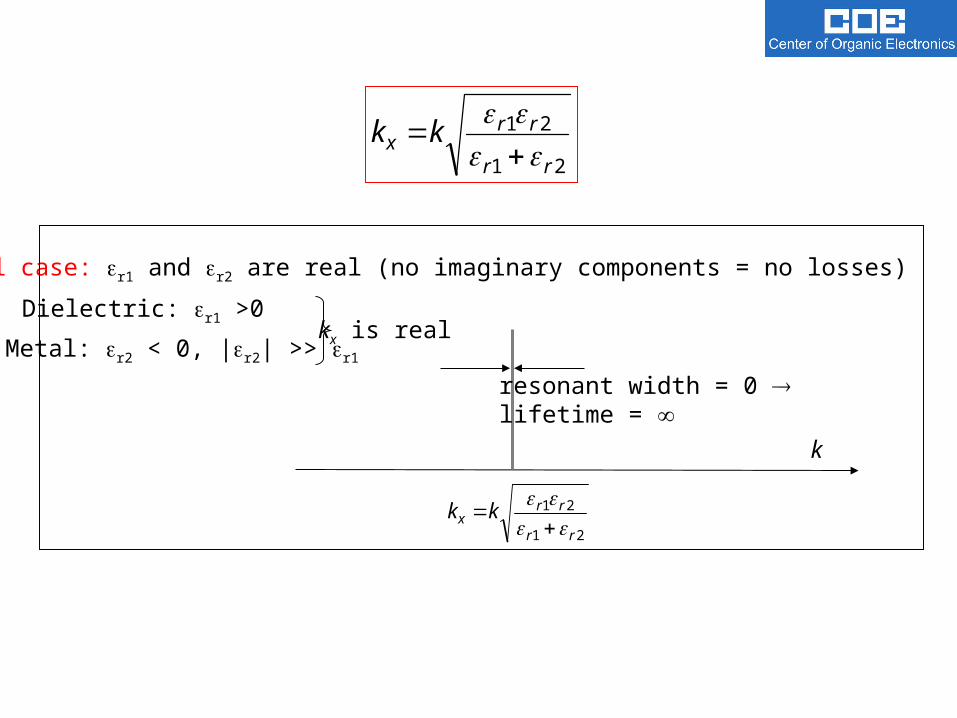
Ideal case: r1 and r2 are real (no imaginary components = no losses)
Dielectric: r1 >0
Metal: r2 < 0, |r2| >> r1
k
resonant width = 0 lifetime =
21
21
rr
rrx kk
kx is real
21
21
rr
rrx kk
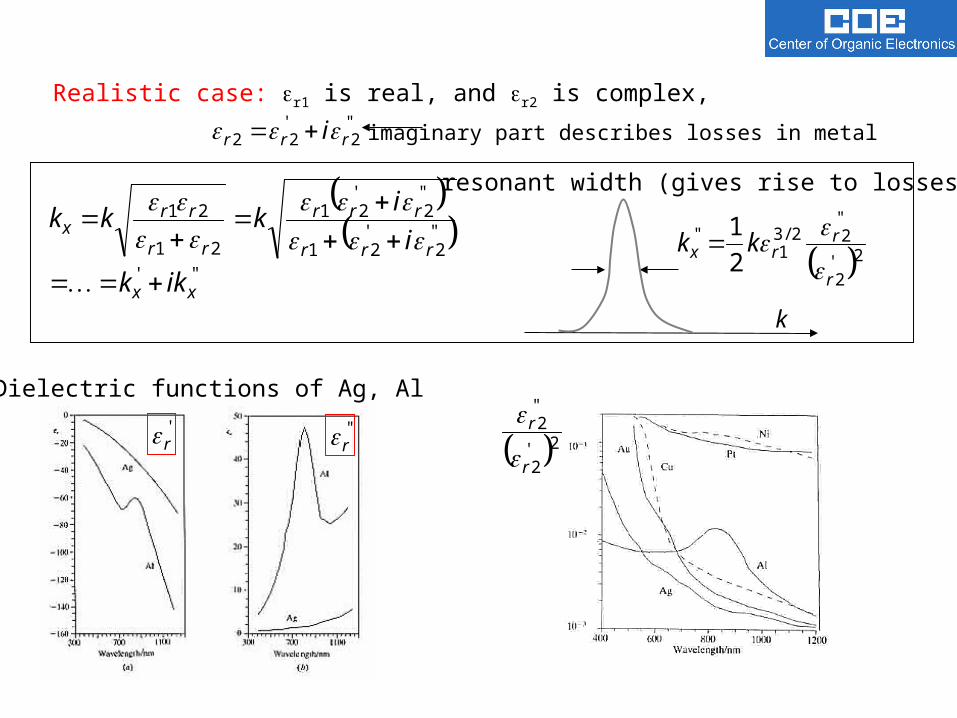
Realistic case: r1 is real, and r2 is complex, ''2
'22 rrr i imaginary part describes losses in metal
'''
''2
'21
''2
'21
21
21
xx
rrr
rrr
rr
rrx
ikk
i
ikkk
k
resonant width (gives rise to losses)
2'2
''22/3
1''
2
1
r
rrx kk
Dielectric functions of Ag, Al
''r
'r 2'
2
''2
r
r
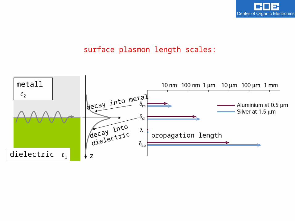
surface plasmon length scales:
dielectric1
metall 2
z
decay into metal
decay into
dielectric propagation length
dielectric1
metall 2
is it possible to excite a plasmon mode by shining light directly on a dielectric/metal interface?
k
kx
21
21
rr
rrx ck
lig
ht co
ne =
c
k
The surface plasmon mode always lie beyond the light line, that is it has greater momentum than a free photon of the same frequency .
This makes a direct excitation of a surface plasmon mode impossible!
OPTICAL EXCITATION OF PLASMONSOPTICAL EXCITATION OF PLASMONS
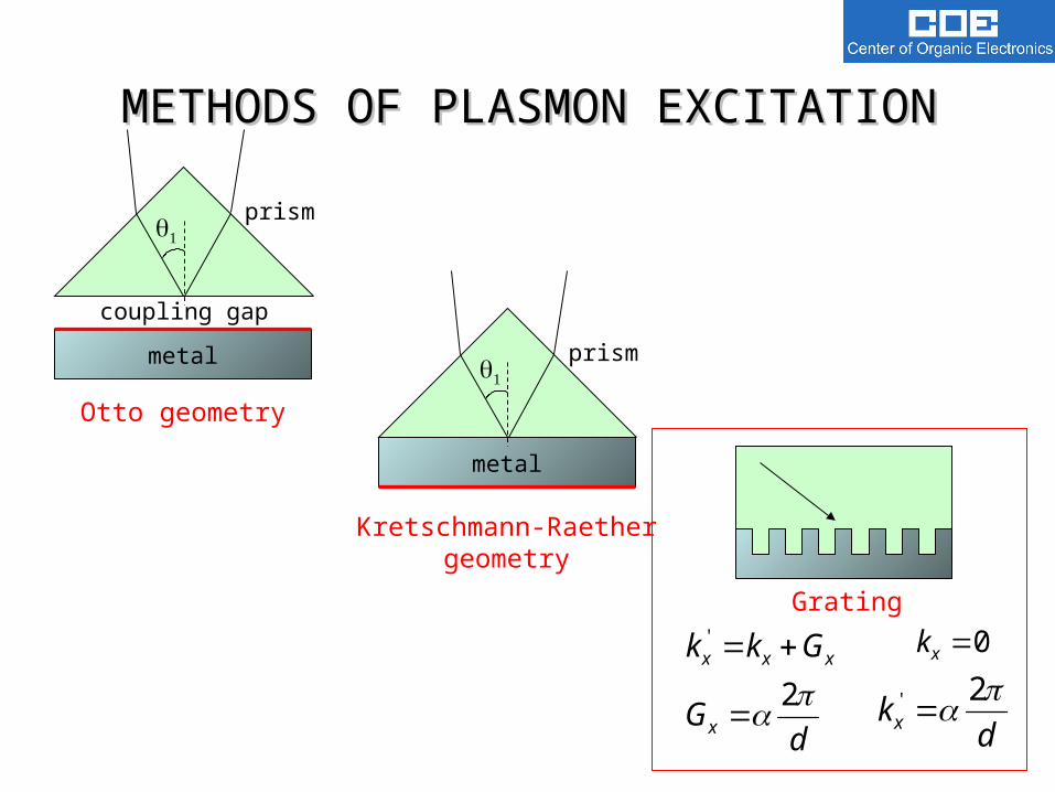
metal
coupling gap
prism
Otto geometry
metal
prism
Kretschmann-Raethergeometry
Grating
dG
Gkk
x
xxx
2
'
dkx
2'
0xk
METHODS OF PLASMON EXCITATIONMETHODS OF PLASMON EXCITATION
Observation of plasmon enhanced absorbtion in
Apfo3/PCBM
Introduction
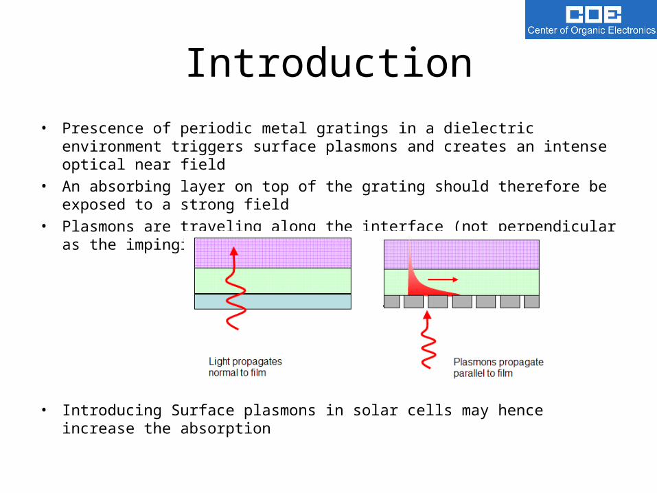
• Prescence of periodic metal gratings in a dielectric environment triggers surface plasmons and creates an intense optical near field
• An absorbing layer on top of the grating should therefore be exposed to a strong field
• Plasmons are traveling along the interface (not perpendicular as the impinging light)
• Introducing Surface plasmons in solar cells may hence increase the absorption
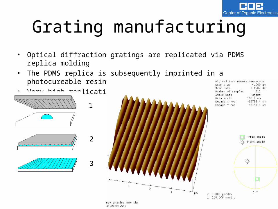
Grating manufacturing
• Optical diffraction gratings are replicated via PDMS replica molding
• The PDMS replica is subsequently imprinted in a photocureable resin.
• Very high replication throughput
1
2
3
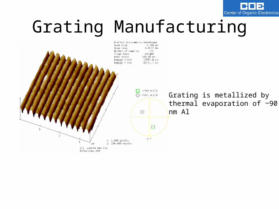
Grating Manufacturing
Grating is metallized by thermal evaporation of ~90 nm Al
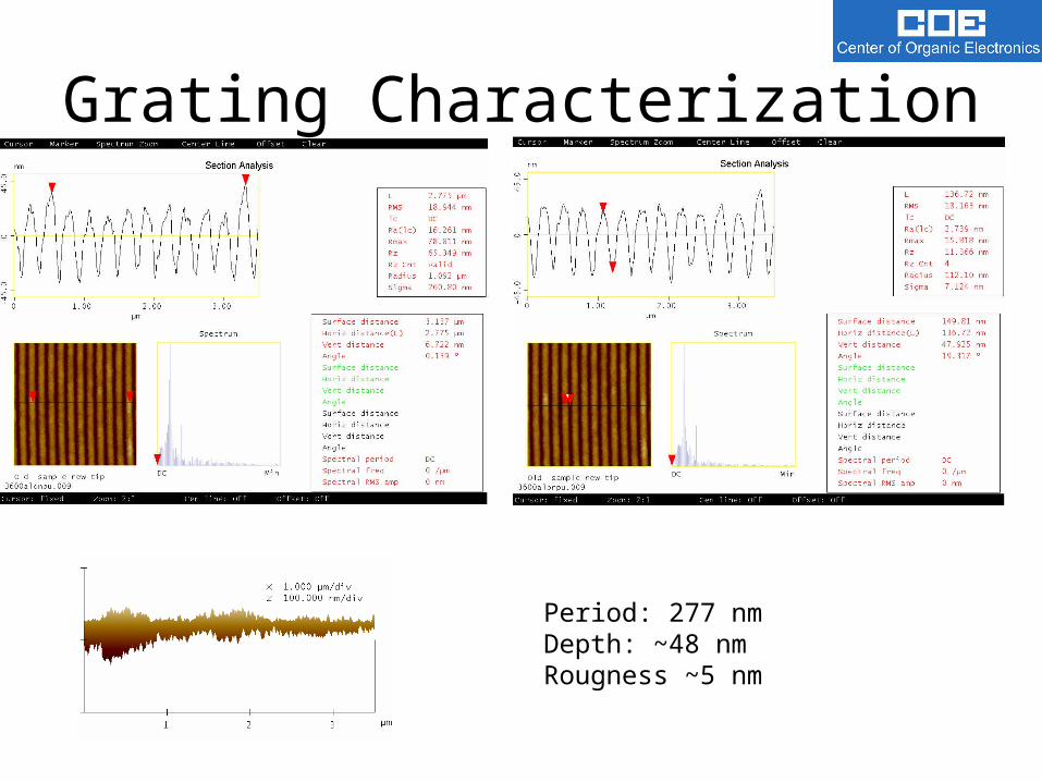
Grating Characterization
Period: 277 nmDepth: ~48 nmRougness ~5 nm
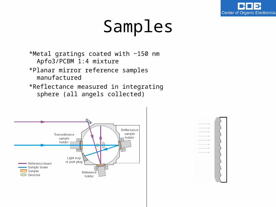
Samples
*Metal gratings coated with ~150 nm Apfo3/PCBM 1:4 mixture
*Planar mirror reference samples manufactured
*Reflectance measured in integrating sphere (all angels collected)
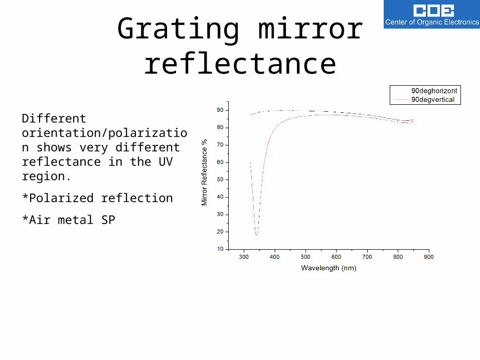
Grating mirror reflectance
Different orientation/polarization shows very different reflectance in the UV region.
*Polarized reflection
*Air metal SP
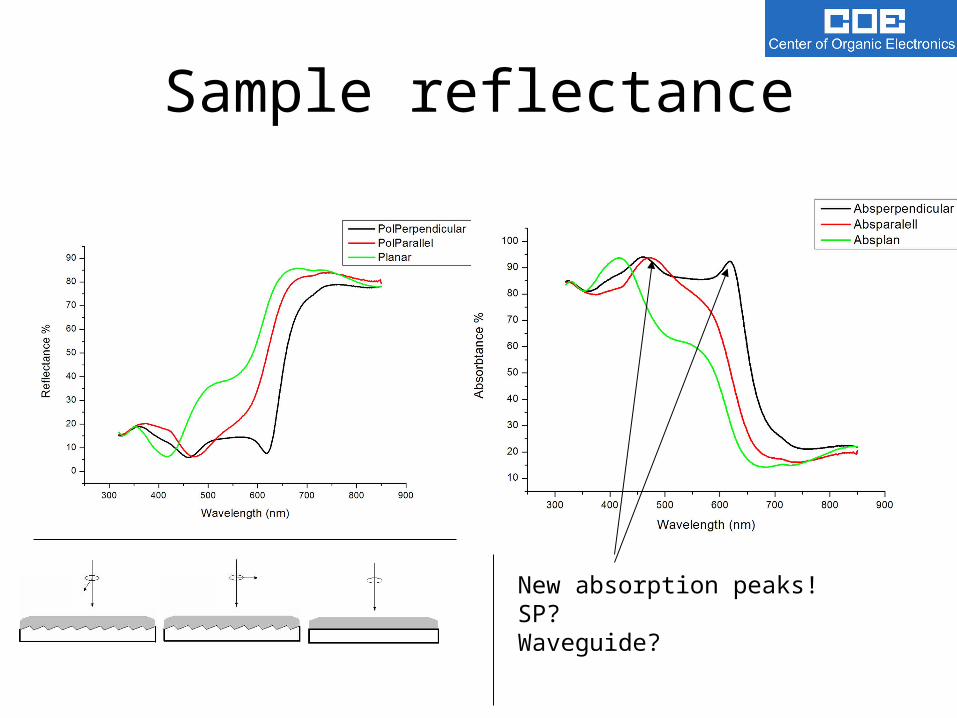
Sample reflectance
New absorption peaks!SP?Waveguide?
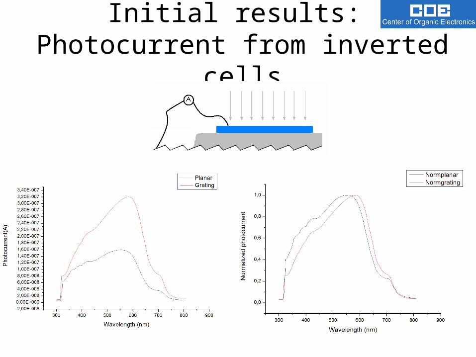
Initial results: Photocurrent from inverted cells
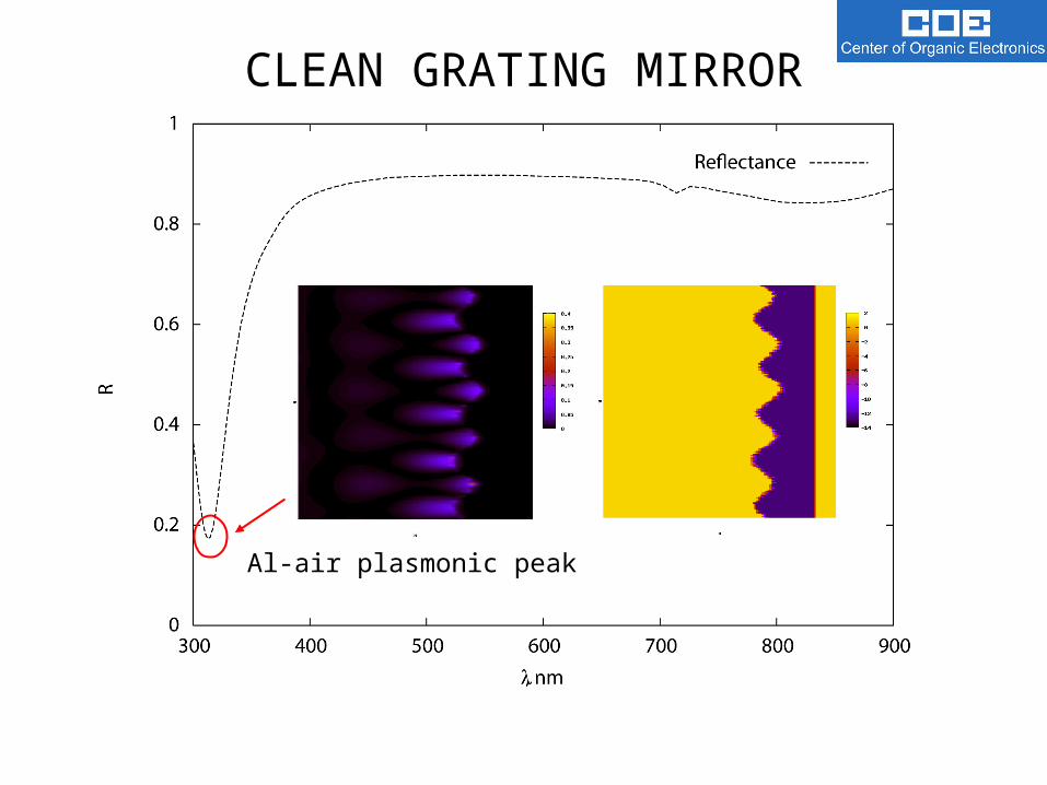
CLEAN GRATING MIRROR
Al-air plasmonic peak
35x106
30
25
20
15
n/c
, m
-1
45x106
403530252015
kx, m-1
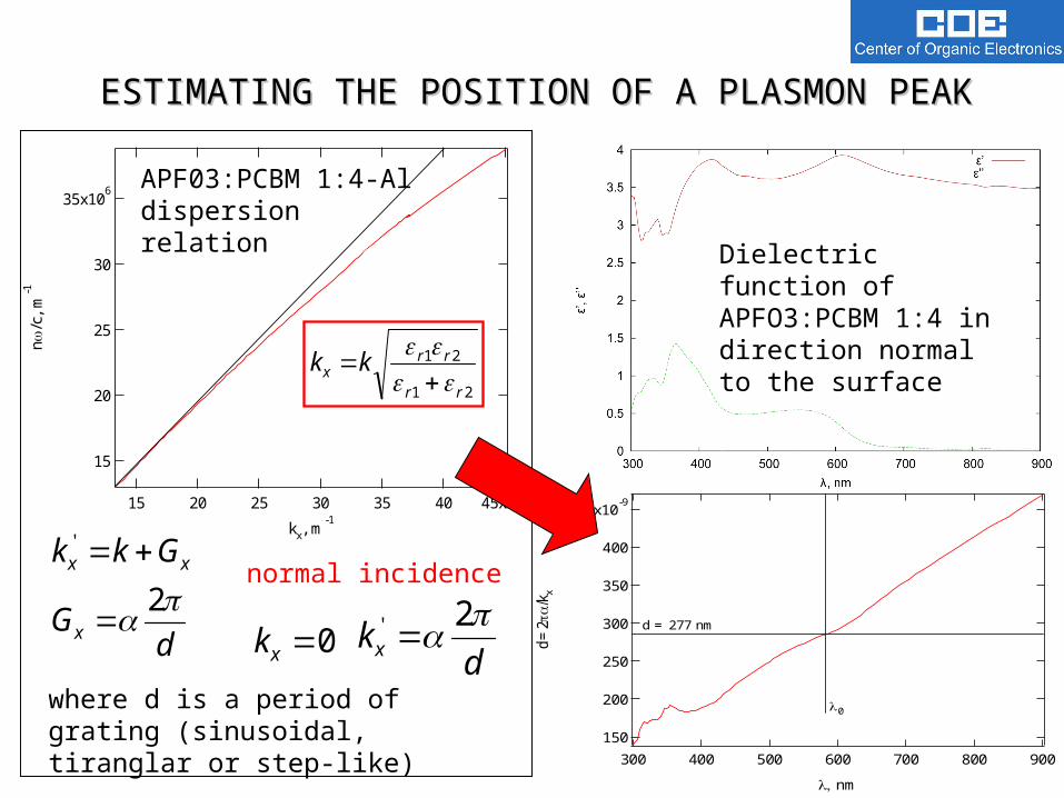
ESTIMATING THE POSITION OF A PLASMON PEAKESTIMATING THE POSITION OF A PLASMON PEAK
APF03:PCBM 1:4-Al dispersion relation
dG
Gkk
x
xx
2
'
dkx
2' 0xk
normal incidence
where d is a period of grating (sinusoidal, tiranglar or step-like)
Dielectric function of APFO3:PCBM 1:4 in direction normal to the surface
450x10-9
400
350
300
250
200
150
d=
2k
x
900800700600500400300
nm
d = 277 nm
0
21
21
rr
rrx kk
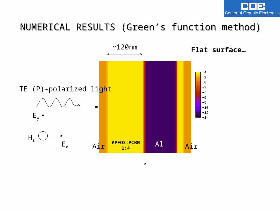
NUMERICAL RESULTS (Green’s function method)NUMERICAL RESULTS (Green’s function method)
AlAPFO3:PCBM1:4Air Air
~120nm
TE (P)-polarized light
Hz
Ey
Ex
Flat surface…

Flat surface and experiment once again...Flat surface and experiment once again...
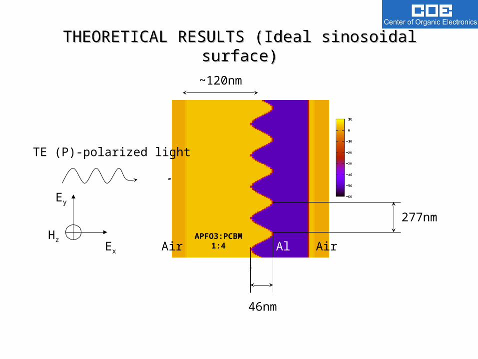
THEORETICAL RESULTS (Ideal sinosoidal surface)THEORETICAL RESULTS (Ideal sinosoidal surface)
AlAPFO3:PCBM
1:4Air Air
~120nm
TE (P)-polarized light
Hz
Ey
Ex
46nm
277nm
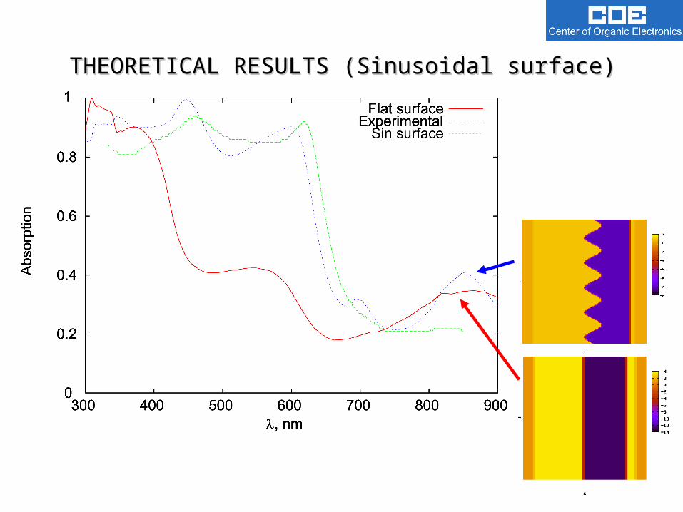
THEORETICAL RESULTS (Sinusoidal surface)THEORETICAL RESULTS (Sinusoidal surface)
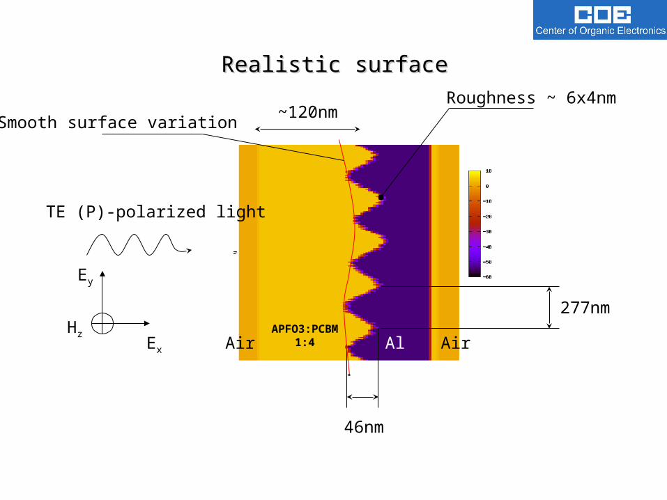
Realistic surfaceRealistic surface
AlAPFO3:PCBM
1:4Air Air
~120nm
TE (P)-polarized light
Hz
Ey
Ex
46nm
277nm
Roughness ~ 6x4nm
Smooth surface variation

Realistic surfaceRealistic surface
25nm

Absoptance peaksAbsoptance peaks
~250 nm thickpolymer
?
CONCLUSIONSCONCLUSIONS
• We demonstrated both experimentally and theretically enchanced absorptance of light in APFO3:PCBM 1:4 solar-cells with Al gratings
• Easy manufacturing with soft lithography.• The theoretical and experimental data agree very
well!
THANKTHANK YOUYOU!!
Acknowledgements
• Nils-Christer Persson for optical characterization of the
materials • Chalmers for materials