Embed Size (px)
Citation preview

User's GuideSLAU221A–May 2007–Revised June 2007
TAS5162DDV6EVM2
This user's guide describes the operation of the evaluation module for the TAS5162Digital Amplifier Power Output Stage using TAS5518 Digital Audio PWM Processorfrom Texas Instruments. The user's guide also provides measurement data and designinformation such as the schematic, BOM, and PCB layout
ContentsTrademarks.......................................................................................... 2
1 Overview ............................................................................................. 22 Quick Setup Guide ................................................................................. 53 Protection ............................................................................................ 74 TAS5162DDV6EVM2 Performance .............................................................. 85 Related Documentation from Texas Instruments ............................................. 20Appendix A .............................................................................................. 21
List of Figures
1 Integrated PurePath Digital™ Amplifier System................................................ 42 Physical structure for the TAS5162DDV6EVM2 (Approximate Layout) ..................... 43 TAS5518 GUI Window............................................................................. 64 THD+N vs Power (BTL - 6Ω) .................................................................... 105 THD+N vs Power (BTL - 8Ω) .................................................................... 106 THD+N vs Power (PBTL - 4Ω) .................................................................. 117 THD+N vs Frequency (BTL - 6Ω)............................................................... 118 THD+N vs Frequency (BTL - 8Ω)............................................................... 129 THD+N vs Frequency (PBTL - 4Ω) ............................................................. 1210 Figure 10. FFT Spectrum With -60 dBFS Tone (BTL) ....................................... 1311 4.8 FFT Spectrum With -60 dBFS Tone (PBTL) .............................................. 1312 Idle Noise FFT Spectrum (BTL) ................................................................. 1413 Idle Noise FFT Spectrum (PBTL) ............................................................... 1414 Channel Separation............................................................................... 1515 Frequency Response (BTL) ..................................................................... 1516 Frequency Response (PBTL).................................................................... 1617 High Current Protection (BTL)................................................................... 1618 High Current Protection (PBTL) ................................................................. 1719 Pop/Click (BTL).................................................................................... 1720 Pop/Click (PBTL) .................................................................................. 1821 Output Stage Efficiency .......................................................................... 1822 Subwoofer Line Out THD Vs. Output Voltage ................................................ 1923 Subwoofer Line Out THD+N vs. Frequency ................................................... 1924 Subwoofer Line Out Frequency Response .................................................... 20
List of Tables
1 TAS5162DDV6EVM2 Specification .............................................................. 22 Recommended Supply Voltages ................................................................. 53 TAS5162 Warning/Error Signal Decoding....................................................... 74 General Test Conditions ........................................................................... 8
SLAU221A–May 2007–Revised June 2007 TAS5162DDV6EVM2 1Submit Documentation Feedback
www.ti.com
Trademarks
1 Overview
Overview
5 TAS5518 Register Settings ....................................................................... 86 Electrical Data....................................................................................... 87 Audio Performance ................................................................................. 98 Audio Performance Subwoofer Line Output .................................................... 99 Thermal Specifications............................................................................. 910 Physical pecifications .............................................................................. 911 Related Documentation from Texas Instruments ............................................. 20A-1 Design Documents................................................................................ 21
Topic .................................................................................................. Page
PurePath Digital, Equibit are trademarks of Texas Instruments.
I2C is a trademark of Philips Electronics.
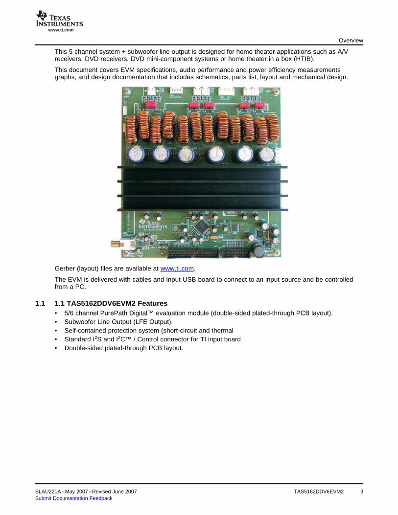
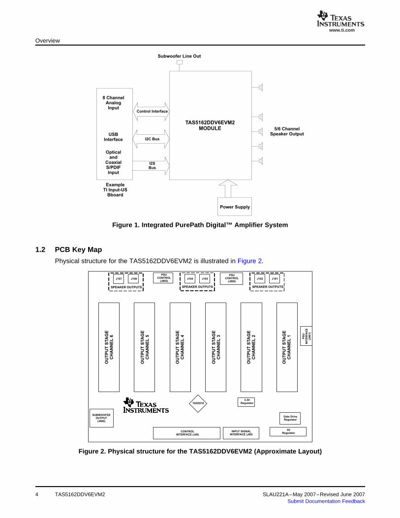
The TAS5162DDV6EVM2 PurePath Digital ™ customer evaluation module demonstrates the integratedcircuits TAS5162DDV and TAS5518PAG from Texas Instruments.
The TAS5162DDV is a high-performance, integrated stereo Digital Amplifier Power Stage designed todrive 6-Ω speakers at up to 210 W per channel. The device incorporates PurePath Digital™ technologyand is designed to be used with PurePath Digital™ modulators. This system requires only a simplepassive demodulation filter to deliver high-quality, high-efficiency audio amplification.
TAS5518PAG is a high performance 32 bit (24 bit input) multi channel PurePath Digital™ Pulse WidthModulator (PWM) based on Equibit™ technology with fully symmetrical AD modulation scheme. Thedevice also has Digital Audio Processing (DAP) that provides 48 bit signal processing, advancedperformance and a high level of system integration. The device has interfaces for headphone output andPower Supply Volume Control (PSVC).
This EVM is configured with 4 BTL channels and 1 PBTL (parallel BTL) channel for the subwooferchannel.
This EVM, together with a TI input-USB board, is a complete 5 channels + subwoofer line output digitalaudio amplifier system which includes digital input (S/PDIF), analog inputs, interface to PC and DAPfeatures like digital volume control, input and output mixers, automute, tone controls, loudness, EQ filtersand dynamic range compression (DRC). There are configuration option for power stage failure protectionand a mini-jack connector for headphone.
Table 1. TAS5162DDV6EVM2 SpecificationKey Parameters
Output Stage Supply Voltage: 0V – 50 V
System Supply Voltage: 15V – 20 V
Number of Channels 4 x BTL, 1x PBTL
Load Impedance BTL: 6-8 Ω
Load Impedance PBTL: 4-8 Ω
Output power BTL 160W / 8 Ω 10% THD or 210W / 6 Ω / 10% THD
Output power PBTL 310W / 4 Ω / 10% THD
DNR >110 dB
PWM Processor TAS5518PAG
Output Stage TAS5162DDV
Other Features Subwoofer line output
TAS5162DDV6EVM22 SLAU221A–May 2007–Revised June 2007Submit Documentation Feedback
www.ti.com
1.1 1.1 TAS5162DDV6EVM2 Features
Overview
This 5 channel system + subwoofer line output is designed for home theater applications such as A/Vreceivers, DVD receivers, DVD mini-component systems or home theater in a box (HTIB).
This document covers EVM specifications, audio performance and power efficiency measurementsgraphs, and design documentation that includes schematics, parts list, layout and mechanical design.
Gerber (layout) files are available at www.ti.com.
The EVM is delivered with cables and Input-USB board to connect to an input source and be controlledfrom a PC.
• 5/6 channel PurePath Digital™ evaluation module (double-sided plated-through PCB layout).• Subwoofer Line Output (LFE Output).• Self-contained protection system (short-circuit and thermal• Standard I2S and I2C™ / Control connector for TI input board• Double-sided plated-through PCB layout.
SLAU221A–May 2007–Revised June 2007 TAS5162DDV6EVM2 3Submit Documentation Feedback
www.ti.com
I2SBus
TAS5162DDV6EVM2MODULE
I2C Bus
ExampleTI Input-US
Bboard
8 ChannelAnalogInput
USBInterface
Opticaland
CoaxialS/PDIFInput
Control Interface
Power Supply
5/6 ChannelSpeaker Output
Subwoofer Line Out
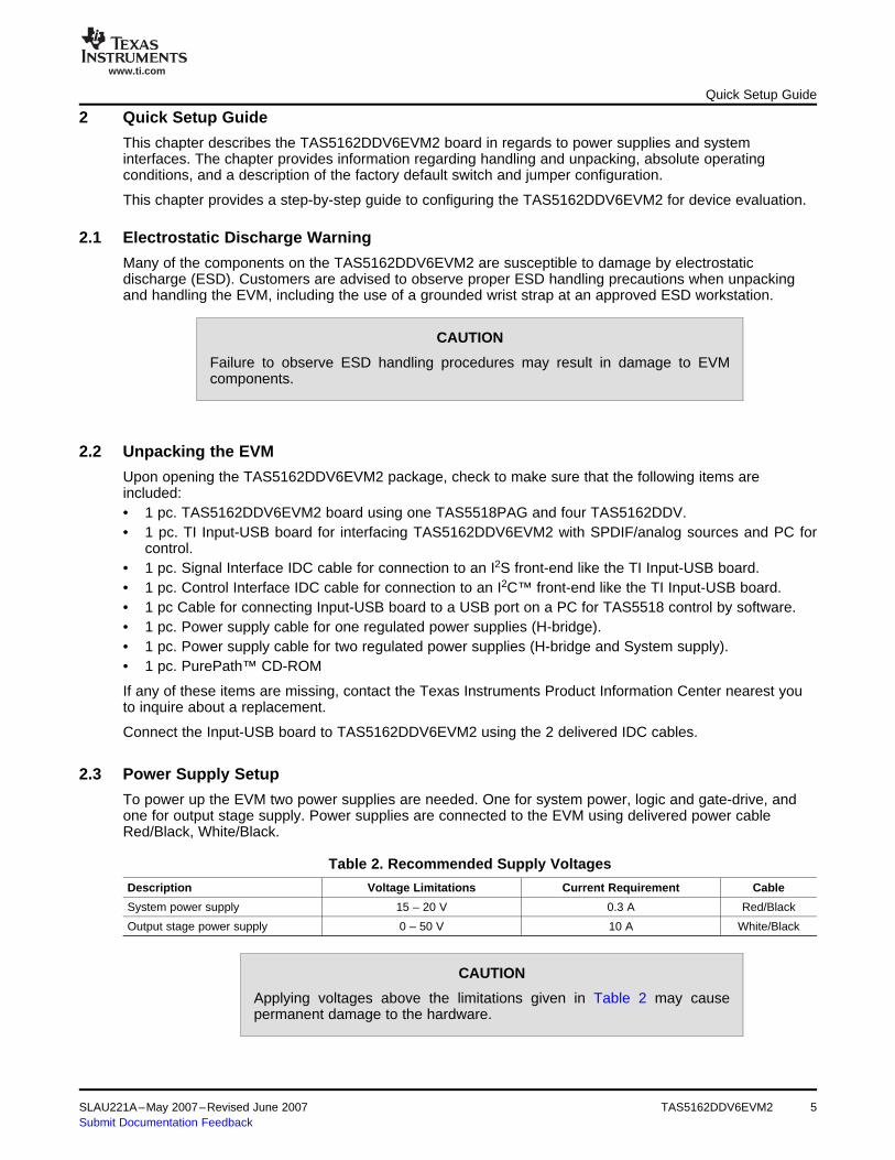
1.2 PCB Key Map
SPEAKER OUTPUTS
TAS55183.3V
Regulator
5VRegulator
Gate DriveRegulator
PS
UIN
TE
RFA
CE
(J9
01
)
INPUT SIGNALINTERFACE (J60)
CONTROLINTERFACE (J40)
SUBWOOFEROUTPUT
(J600)
J101J102
OU
TP
UT
STA
GE
CH
AN
NE
L1SPEAKER OUTPUTS
J103J104
SPEAKER OUTPUTS
J108J107
OU
TP
UT
STA
GE
CH
AN
NE
L6
OU
TP
UT
STA
GE
CH
AN
NE
L5
OU
TP
UT
STA
GE
CH
AN
NE
L4
OU
TP
UT
STA
GE
CH
AN
NE
L3
OU
TP
UT
STA
GE
CH
AN
NE
L2
PSUCONTROL
(J900)
PSUCONTROL
(J902)
Overview
Figure 1. Integrated PurePath Digital™ Amplifier System
Physical structure for the TAS5162DDV6EVM2 is illustrated in Figure 2.
Figure 2. Physical structure for the TAS5162DDV6EVM2 (Approximate Layout)
TAS5162DDV6EVM24 SLAU221A–May 2007–Revised June 2007Submit Documentation Feedback
www.ti.com
2 Quick Setup Guide
2.1 Electrostatic Discharge Warning
2.2 Unpacking the EVM
2.3 Power Supply Setup
Quick Setup Guide
This chapter describes the TAS5162DDV6EVM2 board in regards to power supplies and systeminterfaces. The chapter provides information regarding handling and unpacking, absolute operatingconditions, and a description of the factory default switch and jumper configuration.
This chapter provides a step-by-step guide to configuring the TAS5162DDV6EVM2 for device evaluation.
Many of the components on the TAS5162DDV6EVM2 are susceptible to damage by electrostaticdischarge (ESD). Customers are advised to observe proper ESD handling precautions when unpackingand handling the EVM, including the use of a grounded wrist strap at an approved ESD workstation.
CAUTION
Failure to observe ESD handling procedures may result in damage to EVMcomponents.
Upon opening the TAS5162DDV6EVM2 package, check to make sure that the following items areincluded:• 1 pc. TAS5162DDV6EVM2 board using one TAS5518PAG and four TAS5162DDV.• 1 pc. TI Input-USB board for interfacing TAS5162DDV6EVM2 with SPDIF/analog sources and PC for
control.• 1 pc. Signal Interface IDC cable for connection to an I2S front-end like the TI Input-USB board.• 1 pc. Control Interface IDC cable for connection to an I2C™ front-end like the TI Input-USB board.• 1 pc Cable for connecting Input-USB board to a USB port on a PC for TAS5518 control by software.• 1 pc. Power supply cable for one regulated power supplies (H-bridge).• 1 pc. Power supply cable for two regulated power supplies (H-bridge and System supply).• 1 pc. PurePath™ CD-ROM
If any of these items are missing, contact the Texas Instruments Product Information Center nearest youto inquire about a replacement.
Connect the Input-USB board to TAS5162DDV6EVM2 using the 2 delivered IDC cables.
To power up the EVM two power supplies are needed. One for system power, logic and gate-drive, andone for output stage supply. Power supplies are connected to the EVM using delivered power cableRed/Black, White/Black.
Table 2. Recommended Supply Voltages
Description Voltage Limitations Current Requirement Cable
System power supply 15 – 20 V 0.3 A Red/Black
Output stage power supply 0 – 50 V 10 A White/Black
CAUTION
Applying voltages above the limitations given in Table 2 may causepermanent damage to the hardware.
SLAU221A–May 2007–Revised June 2007 TAS5162DDV6EVM2 5Submit Documentation Feedback
www.ti.com
2.4 Speaker Connection
2.5 GUI Software Installation
Quick Setup Guide
Note: The length of power supply cable must be minimized. Increasing length of PSUcable is equal to increasing the distortion for the amplifier at high output levels andlow frequencies.
CAUTION
Both positive and negative speaker outputs are floating and may not beconnected to ground (e.g. through an oscilloscope).
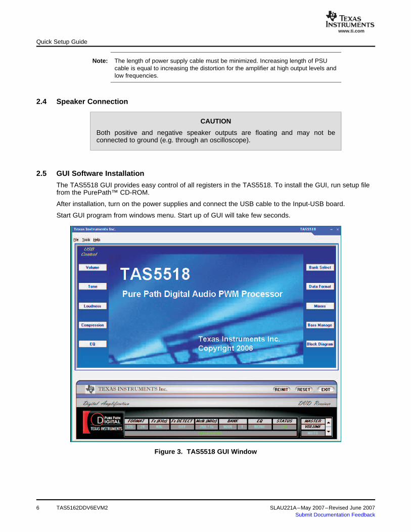
The TAS5518 GUI provides easy control of all registers in the TAS5518. To install the GUI, run setup filefrom the PurePath™ CD-ROM.
After installation, turn on the power supplies and connect the USB cable to the Input-USB board.
Start GUI program from windows menu. Start up of GUI will take few seconds.
Figure 3. TAS5518 GUI Window
6 TAS5162DDV6EVM2 SLAU221A–May 2007–Revised June 2007Submit Documentation Feedback
www.ti.com
3 Protection
3.1 Short Circuit Protection and Fault Reporting Circuitry
3.2 Fault Reporting
Protection
From the files menu load the configuration file:TAS5162DDV6EVM2 Configuration (1.00).cfg
The file is located on the PurePath™ CD-rom. This file contains all settings for a default setup of the EVM.
For easy access of the file it is recommended to copy the files into directory where the GUI is installed.Default is C:\Program Files\Texas Instruments Inc\TAS5518\
For more advanced use of the GUI, refer to the GUI User’s Guide and data manual for the TAS5518.
This chapter describes the short-circuit protection and fault reporting circuitry of the TAS5162 (SLES194)device.
The TAS5162 is a self-protecting device that provides fault reporting (including high-temperatureprotection and short-circuit protection). TAS5162 is configured in back-end auto-recovery mode, andtherefore, resets automatically after all errors (M1, M2 and M3 is set low), see the data sheet for furtherexplanation. This mean that the device will restart it self after an error occasion and report shortly throughthe SD error signal.
The OTW and SD outputs from TAS5162 indicate fault conditions. See the TAS5162 data manual for adescription of these pins.
Table 3. TAS5162 Warning/Error Signal Decoding
OTW SD Device Condition
0 0 High temperature error and/or high current error
0 1 High temperature warning
1 0 Undervoltage lockout or high current error
1 1 Normal operation, no errors/warnings
The temperature warning signals at the TAS5162DDV6EVM2 board are wired — or to one temperaturewarning signal (OTW – pin 22 in control interface connector). Shutdown signals are wired-or into oneshutdown signal (SD – pin 20 in control interface connector).
The shutdown signals together with the temperature warning signal give chip state information asdescribed in Table 3. Device fault reporting outputs are open-drain outputs.
SLAU221A–May 2007–Revised June 2007 TAS5162DDV6EVM2 7Submit Documentation Feedback
www.ti.com
4 TAS5162DDV6EVM2 PerformanceTAS5162DDV6EVM2 Performance
All electrical and audio specifications are typical values.
Table 4. General Test Conditions
General Test Conditions (1) Notes
Output Stage Supply Voltage: 50 V Laboratory Power Supply (EA-PS 7065-10A)
System Supply Voltage: 15 V
Load Impedance BTL: 6-8 Ω
Load Impedance PBTL: 3-4 Ω
Input Signal 1kHz Sine
Sampling Frequency 48 kHz
Gain setting in TAS5518 0 dB
Measurement Filter AES17 and AUX0025
TI Input-USB Board Input-USB Rev 10
EVM configuration file Ver 1.00 TAS5162DDV6EVM2 Configuration (1.00).cfg
(1) These test conditions are used for all tests, unless otherwise specified.
Table 5. TAS5518 Register Settings
Register (1) Value Notes
Modulation Index Limit Register 0x16 0x04 Set Modulation Index to 96.1%
Master Volume Register 0xD9 00 00 00 48 Master Volume set to 0 dB
(1) These register settings are used for all test, unless otherwise specified.
Table 6. Electrical Data
Electrical Data Notes/Conditions
Output Power, BTL, 6 Ω: 155 W 1 kHz, unclipped (0 dBFS), TA = 25°C
Output Power, BTL, 6 Ω: 210 W 1 kHz, 10% THD+N, TA = 25°C
Output Power, BTL, 8 Ω: 125 W 1 kHz, unclipped (0 dBFS), TA = 25°C
Output Power, BTL, 8 Ω: 160 W 1 kHz, 10% THD+N, TA = 25°C
Output Power, PBTL, 4 Ω: 240 W 1 kHz, unclipped (0 dBFS), TA = 25°C
Output Power, PBTL, 4 Ω: 315 W 1 kHz, 10% THD+N, TA = 25°C
Maximum Peak Current, BTL: >10 A 1 kHz burst, 1 Ω, ROC = 22k
Maximum Peak Current, PBTL: >20 A 1 kHz burst, 1 Ω, ROC = 22k
Output Stage Efficiency: 90% 2 x channels, 8 Ω
Damping Factor BTL: 15 1 kHz, relative to 8 Ω load
Damping Factor PBTL: 15 1 kHz, relative to 4 Ω load
System Supply Current: <270 mA 1 kHz, -60 dBFS signal, with TI input board
H-Bridge Supply Current: <187 mA 1 kHz, -60 dBFS signal
Total Board Idle Power Consumption: 13.4 W H-Bridge supply + System supply, -60 dBFS signal
8 TAS5162DDV6EVM2 SLAU221A–May 2007–Revised June 2007Submit Documentation Feedback
www.ti.com
TAS5162DDV6EVM2 Performance
Table 7. Audio Performance
Audio Performance Notes/Conditions
THD+N, BTL, 6 Ω: 1 W <0.02% 1 kHz
THD+N, BTL, 6 Ω: 10 W <0.06% 1 kHz
THD+N, BTL, 6 Ω: 50 W <0.10% 1 kHz
THD+N, BTL, 6 Ω: 100 W <0.10% 1 kHz
THD+N, BTL, 6 Ω: 150 W <0.13% 1 kHz
THD+N, BTL, 8 Ω: 1 W <0.02% 1 kHz
THD+N, BTL, 8 Ω: 10 W <0.06% 1 kHz
THD+N, BTL, 8 Ω: 50 W <0.08% 1 kHz
THD+N, BTL, 8 Ω: 100 W <0.07% 1 kHz
THD+N, PBTL, 4 Ω: 1 W <0.009% 1 kHz
THD+N, PBTL, 4 Ω: 10 W <0.05% 1 kHz
THD+N, PBTL, 4 Ω: 50 W <0.04% 1 kHz
THD+N, PBTL, 4 Ω: 100 W <0.05% 1 kHz
THD+N, PBTL, 4 Ω: 200 W <0.12% 1 kHz
Dynamic Range: >109 dB Ref: rated power, A-weighted, AES17 filter, 4 ch avg
Noise Voltage: <110 µVrms A-weighted, AES17 filter
Click/Pop, DC step BTL: 10 mV Mute/Unmute, No signal, 6 Ω
Click/Pop, DC step PBTL: 23 mV Mute/Unmute, No signal, 4 Ω
Channel Separation: >65 dB 1 kHz
Frequency Response: +0.8 / 0.0 dB 125 W / 8 Ω, unclipped (0 dBFS)
Table 8. Audio Performance Subwoofer Line Output
Audio Performance Notes/Conditions
Full Scale Output Voltage Swing, 0 dBFS: 1.275 Vrms 1 kHz, 10 kΩ load
Full Scale Output Voltage Swing, 10 % 1 kHz, 10 kΩ load1.5 VrmsTHD+N:
THD+N, 10 kΩ: 1 V <0.009% 1 kHz
THD+N, 10 kΩ: 100 mV <0.01% 1 kHz
Frequency Response: +1, -4 dB 20 Hz – 20 kHz
Dynamic Range: >102 dB 20 Hz – 20 kHz
Noise Voltage: <10 µV 20 Hz – 20 kHz
Table 9. Thermal Specifications
Thermal Specifications THEATSINK(1) Notes/Conditions
Idle, All Channels Switching 41°C 1 kHz, 15 min, -60 dBFS signal, TA = 25°C 1 kHz
6 x 16 W, 8 Ω + 1 x 32 W , 4 Ω (1/8 power) 63°C 1 hour, TA = 25°C
2 x 125 W, 8 Ω 76°C 1 kHz, 5 min, TA = 25°C
(1) Measured on surface of heatsink.
Table 10. Physical pecifications
Physical Specification Notes/Conditions
PCB Dimensions: 160 x 172 x 55 Width x Length x Height (mm)
Total Weight: 640 gr. Components + PCB + Heat-sink + Mechanics
SLAU221A–May 2007–Revised June 2007 TAS5162DDV6EVM2 9Submit Documentation Feedback
www.ti.com
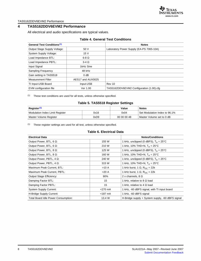
4.1 THD+N vs Power (BTL - 6Ω)
0.005
10
0.01
0.02
0.05
0.1
0.2
0.5
1
2
5
To
tal
Ha
rm
on
ic D
isto
rti
on
+ N
ois
e -
%
20m 40050m 100m 200m 500m 1 2 5 10 20 50 100
Power - W
200
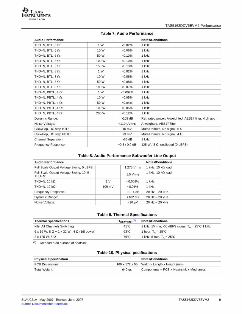
4.2 THD+N vs Power (BTL - 8Ω)
To
tal H
arm
on
ic D
isto
rtio
n +
No
ise
- %
Power - W
0.005
10
0.01
0.02
0.05
0.1
0.2
0.5
1
2
5
20m 20050m 100m 200m 500m 1 2 5 10 20 50 100
TAS5162DDV6EVM2 Performance
Gain: 2.5 dB set in TAS5518
Figure 4. THD+N vs Power (BTL - 6Ω)
Gain: 2.5 dB set in TAS5518
Figure 5. THD+N vs Power (BTL - 8Ω)
TAS5162DDV6EVM210 SLAU221A–May 2007–Revised June 2007Submit Documentation Feedback
www.ti.com
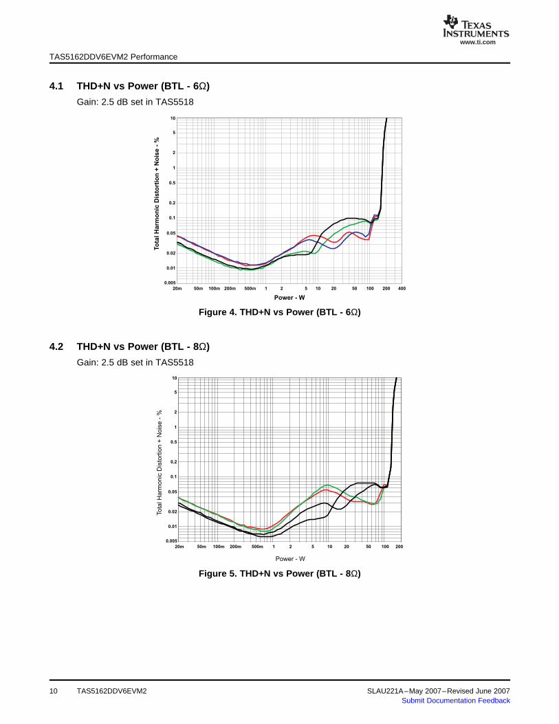
4.3 THD+N vs Power (PBTL - 4Ω)
To
tal
Ha
rm
on
ic D
isto
rti
on
+ N
ois
e -
%
Power - W
0.005
10
0.01
0.02
0.05
0.1
0.2
0.5
1
2
5
20m 50050m 100m 200m 500m 1 2 5 10 20 50 100 200
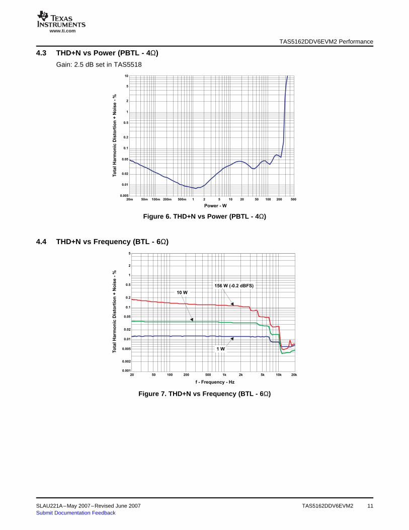
4.4 THD+N vs Frequency (BTL - 6Ω)
To
tal
Ha
rmo
nic
Dis
tort
ion
+ N
ois
e -
%
f - Frequency - Hz
0.001
5
0.002
0.005
0.01
0.02
0.05
0.1
0.2
0.5
1
2
20 20k50 100 200 500 1k 2k 5k 10k
1 W
10 W
156 W (-0.2 dBFS)
TAS5162DDV6EVM2 Performance
Gain: 2.5 dB set in TAS5518
Figure 6. THD+N vs Power (PBTL - 4Ω)
Figure 7. THD+N vs Frequency (BTL - 6Ω)
SLAU221A–May 2007–Revised June 2007 TAS5162DDV6EVM2 11Submit Documentation Feedback
www.ti.com
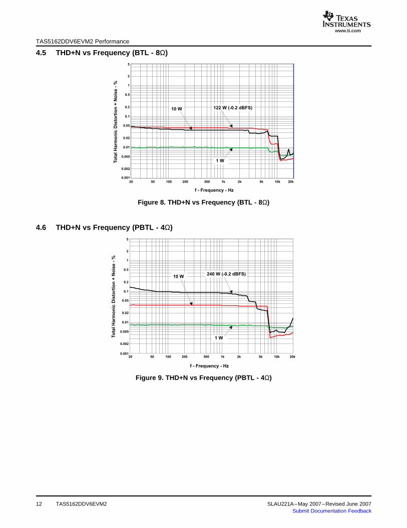
4.5 THD+N vs Frequency (BTL - 8Ω)
To
tal
Ha
rmo
nic
Dis
tort
ion
+ N
ois
e -
%
f - Frequency - Hz
0.001
5
0.002
0.005
0.01
0.02
0.05
0.1
0.2
0.5
1
2
20 20k50 100 200 500 1k 2k 5k 10k
1 W
10 W 122 W (-0.2 dBFS)
4.6 THD+N vs Frequency (PBTL - 4Ω)
To
tal
Ha
rmo
nic
Dis
tort
ion
+ N
ois
e -
%
f - Frequency - Hz
0.001
5
0.002
0.005
0.01
0.02
0.05
0.1
0.2
0.5
1
2
20 20k50 100 200 500 1k 2k 5k 10k
1 W
10 W240 W (-0.2 dBFS)
TAS5162DDV6EVM2 Performance
Figure 8. THD+N vs Frequency (BTL - 8Ω)
Figure 9. THD+N vs Frequency (PBTL - 4Ω)
TAS5162DDV6EVM212 SLAU221A–May 2007–Revised June 2007Submit Documentation Feedback

www.ti.com
4.7 FFT Spectrum With -60 dBFS Tone (BTL)
d
B
Am
pli
tud
e -
dB
f - Frequency - Hz
20k 22k0
-80
4k 8k 12k 14k 16k 18k10k6k2k-150
-140
-130
-120
-110
-100
-70
-60
-40
-90
-30
-20
0
-50
-10
4.8 FFT Spectrum With -60 dBFS Tone (PBTL)
Am
pli
tud
e -
dB
f - Frequency - Hz
20k 22k0
-80
4k 8k 12k 14k 16k 18k10k6k2k-150
-140
-130
-120
-110
-100
-70
-60
-40
-90
-30
-20
0
-50
-10
TAS5162DDV6EVM2 Performance
Reference voltage is 31.9 V. FFT size 16k.
Figure 10. Figure 10. FFT Spectrum With -60 dBFS Tone (BTL)
Reference voltage is 31.7 V. FFT size 16k.
Figure 11. 4.8 FFT Spectrum With -60 dBFS Tone (PBTL)
SLAU221A–May 2007–Revised June 2007 TAS5162DDV6EVM2 13Submit Documentation Feedback
www.ti.com
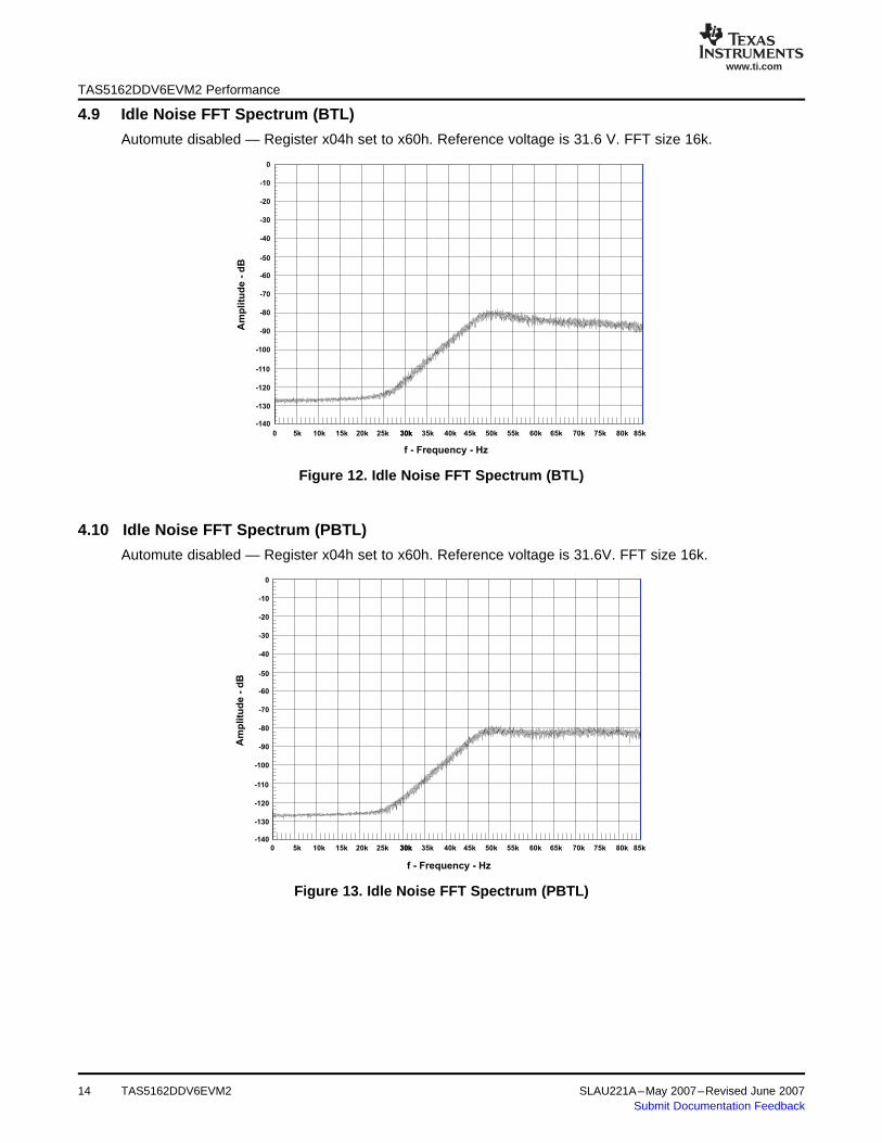
4.9 Idle Noise FFT Spectrum (BTL)
d
B
Am
pli
tud
e -
dB
f - Frequency - Hz
75k 80k0
-80
10k 25k 45k 55k 60k 70k35k20k5k
-140
-130
-120
-110
-100
-70
-60
-40
-90
-30
-20
0
-50
-10
15k 30k 40k30k 50k 65k 85k
4.10 Idle Noise FFT Spectrum (PBTL)
d
B
Am
pli
tud
e -
dB
f - Frequency - Hz
75k 80k
-80
10k 25k 45k 55k 60k 70k35k20k0-140
-130
-120
-110
-100
-70
-60
-40
-90
-30
-20
0
-50
-10
15k 30k 40k30k 50k 65k 85k5k
TAS5162DDV6EVM2 Performance
Automute disabled — Register x04h set to x60h. Reference voltage is 31.6 V. FFT size 16k.
Figure 12. Idle Noise FFT Spectrum (BTL)
Automute disabled — Register x04h set to x60h. Reference voltage is 31.6V. FFT size 16k.
Figure 13. Idle Noise FFT Spectrum (PBTL)
TAS5162DDV6EVM214 SLAU221A–May 2007–Revised June 2007Submit Documentation Feedback
www.ti.com
4.11 Channel Separation
Am
pli
tud
e -
dB
f - Frequency - Hz
-80
10
-75
-70
-65
-60
-55
-50
-45
-40
-35
-30
-25
-20
-15
-10
-5
0
5
20 20k50 100 200 500 1k 2k 5k 10k
Channel 2
Channel 1
4.12 Frequency Response (BTL)
d
B
Am
pli
tud
e -
dB
f - Frequency - Hz
20
-4
100 1k 5k50050-10
-8
-2
2
-6
4
6
10
0
8
200 30k 10k 20k
8 W
6 W
TAS5162DDV6EVM2 Performance
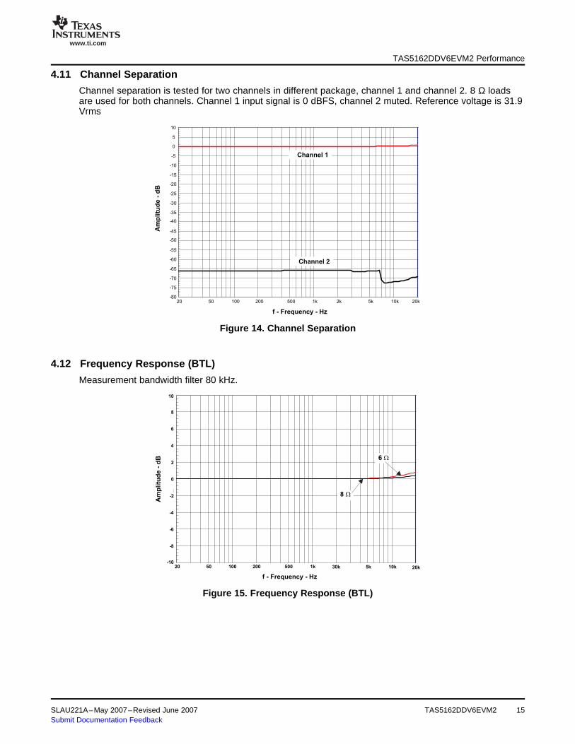
Channel separation is tested for two channels in different package, channel 1 and channel 2. 8 Ω loadsare used for both channels. Channel 1 input signal is 0 dBFS, channel 2 muted. Reference voltage is 31.9Vrms
Figure 14. Channel Separation
Measurement bandwidth filter 80 kHz.
Figure 15. Frequency Response (BTL)
SLAU221A–May 2007–Revised June 2007 TAS5162DDV6EVM2 15Submit Documentation Feedback
www.ti.com
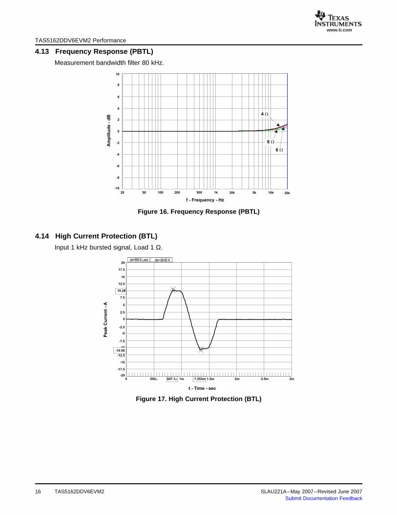
4.13 Frequency Response (PBTL)
Am
pli
tud
e -
dB
f - Frequency - Hz
20
-4
100 1k 5k50050
-10
-8
-2
2
-6
4
6
10
0
8
200 30k 10k 20k
6 W
4 W
8 W
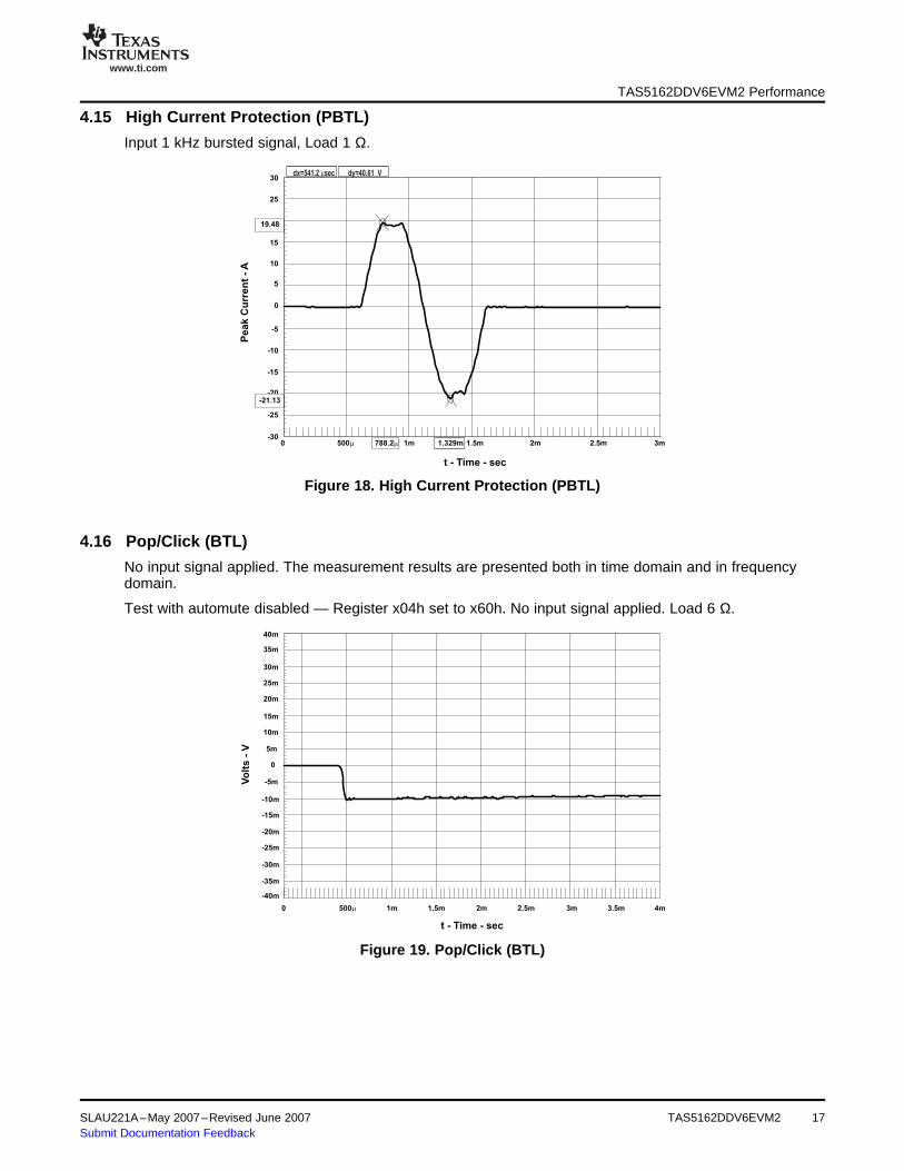
4.14 High Current Protection (BTL)
Pe
ak
Cu
rre
nt
-A
t - Time - sec
0
500m 1.5m 2.5m1m0
-10
-20
-2.5
7.5
-7.5
12.5
15
20
-5
17.5
2m 3m
10
dx=505.9 secm dy=-20.83 V
2.5
5
-12.5
-15
-17.5
10.28
-10.56
1.353m847.1m
TAS5162DDV6EVM2 Performance
Measurement bandwidth filter 80 kHz.
Figure 16. Frequency Response (PBTL)
Input 1 kHz bursted signal, Load 1 Ω.
Figure 17. High Current Protection (BTL)
TAS5162DDV6EVM216 SLAU221A–May 2007–Revised June 2007Submit Documentation Feedback
www.ti.com
4.15 High Current Protection (PBTL)
Pe
ak
Cu
rre
nt
-A
t - Time - sec
0
500m 1.5m 2.5m1m0
-20
-30
-10
10
-15
15
30
-5
25
2m 3m
5
-25
1.329m
20
dx=541.2 secm dy=40.61 V
19.48
-21.13
788.2m
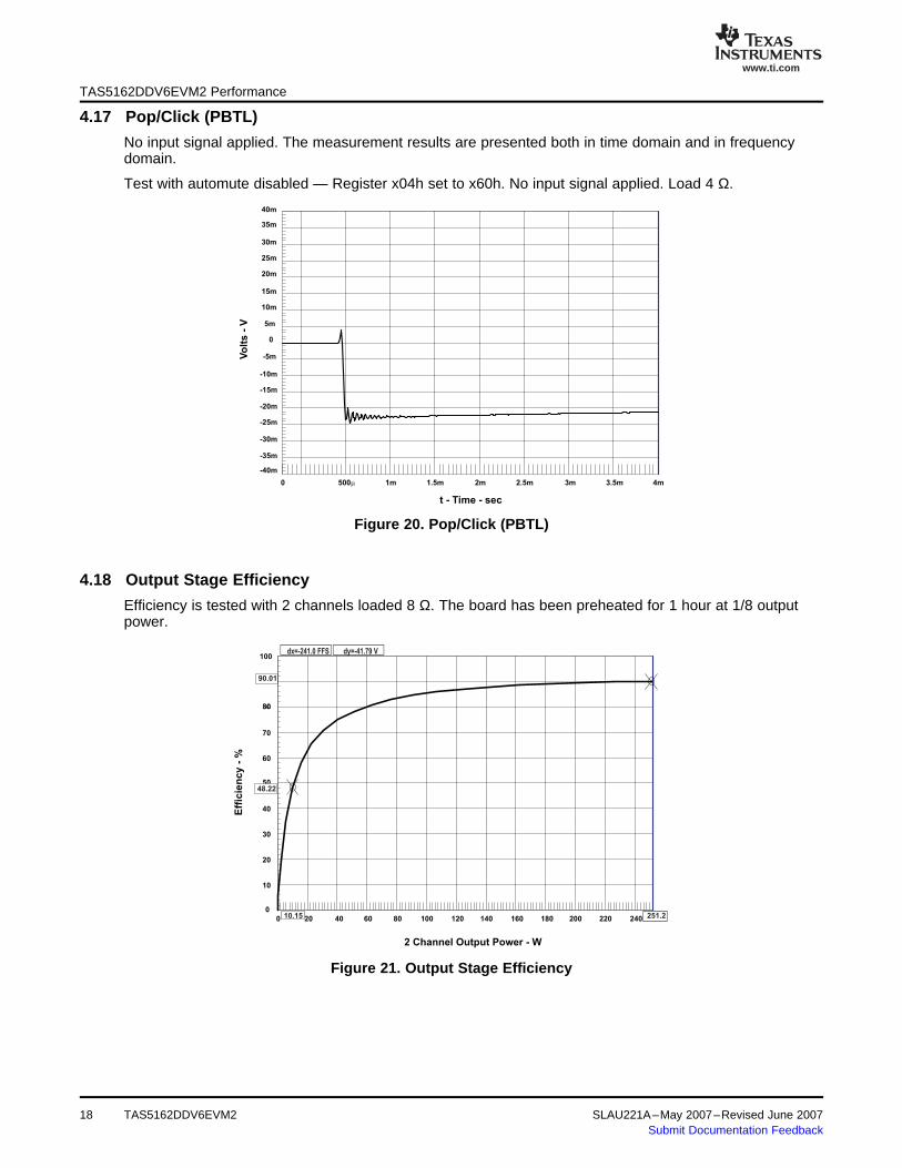
4.16 Pop/Click (BTL)
Vo
lts
- V
t - Time - sec
-40m
40m
-35m
-30m
-25m
-20m
-15m
-10m
-5m
0
5m
10m
15m
20m
25m
30m
35m
0 4m500m 1m 1.5m 2m 2.5m 3m 3.5m
TAS5162DDV6EVM2 Performance
Input 1 kHz bursted signal, Load 1 Ω.
Figure 18. High Current Protection (PBTL)
No input signal applied. The measurement results are presented both in time domain and in frequencydomain.
Test with automute disabled — Register x04h set to x60h. No input signal applied. Load 6 Ω.
Figure 19. Pop/Click (BTL)
SLAU221A–May 2007–Revised June 2007 TAS5162DDV6EVM2 17Submit Documentation Feedback
www.ti.com
4.17 Pop/Click (PBTL)
Vo
lts
- V
t - Time - sec
-40m
40m
-35m
-30m
-25m
-20m
-15m
-10m
-5m
0
5m
10m
15m
20m
25m
30m
35m
0 4m500m 1m 1.5m 2m 2.5m 3m 3.5m
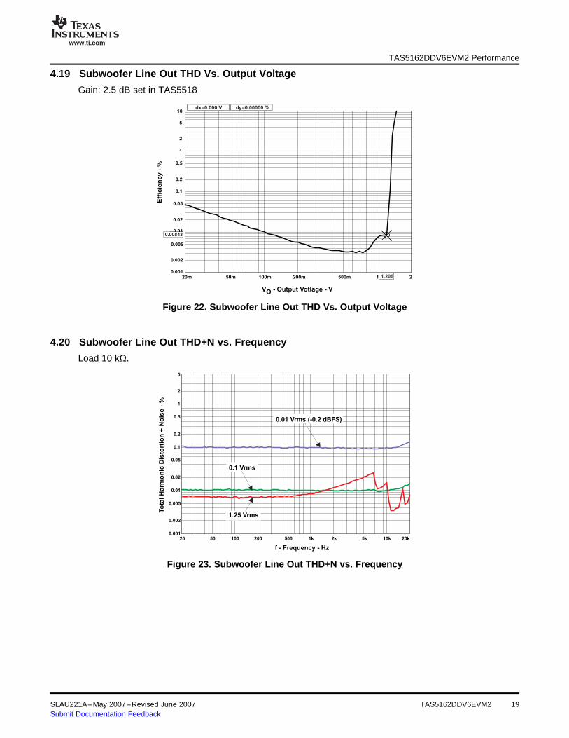
4.18 Output Stage Efficiency
Eff
icie
nc
y -
%
2 Channel Output Power - W
0
100
10
20
30
40
50
60
70
8090
90.01
48.22
0 24020 40 60 80 100 120 140 160 180 200 220 251.210.15
dx=-241.0 FFS dy=-41.79 V
TAS5162DDV6EVM2 Performance
No input signal applied. The measurement results are presented both in time domain and in frequencydomain.
Test with automute disabled — Register x04h set to x60h. No input signal applied. Load 4 Ω.
Figure 20. Pop/Click (PBTL)
Efficiency is tested with 2 channels loaded 8 Ω. The board has been preheated for 1 hour at 1/8 outputpower.
Figure 21. Output Stage Efficiency
TAS5162DDV6EVM218 SLAU221A–May 2007–Revised June 2007Submit Documentation Feedback
www.ti.com
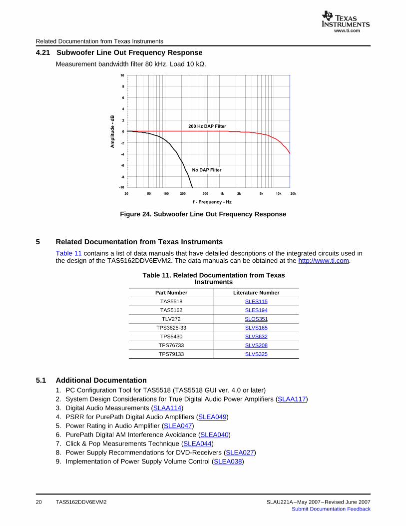
4.19 Subwoofer Line Out THD Vs. Output Voltage
Eff
icie
nc
y -
%
V - Output Votlage - VO
0.001
10
0.002
0.005
0.01
0.02
0.05
0.1
0.2
0.5
1
2
5
0.008430.00843
20m 250m 100m 200m 500m 1 1.2061.206
dx=0.000 V dy=0.00000 %
4.20 Subwoofer Line Out THD+N vs. Frequency
To
tal
Ha
rmo
nic
Dis
tort
ion
+ N
ois
e -
%
f - Frequency - Hz
0.001
5
0.002
0.005
0.01
0.02
0.05
0.1
0.2
0.5
1
2
20 20k50 100 200 500 1k 2k 5k 10k
0.1 Vrms
0.01 Vrms (-0.2 dBFS)
1.25 Vrms
TAS5162DDV6EVM2 Performance
Gain: 2.5 dB set in TAS5518
Figure 22. Subwoofer Line Out THD Vs. Output Voltage
Load 10 kΩ.
Figure 23. Subwoofer Line Out THD+N vs. Frequency
SLAU221A–May 2007–Revised June 2007 TAS5162DDV6EVM2 19Submit Documentation Feedback
www.ti.com
4.21 Subwoofer Line Out Frequency Response
Am
pli
tud
e -
dB
f - Frequency - Hz
-10
10
-6
-4
-2
0
2
4
6
8
20 20k50 100 200 500 1k 2k 5k 10k
-8
200 Hz DAP Filter
No DAP Filter
5 Related Documentation from Texas Instruments
5.1 Additional Documentation
Related Documentation from Texas Instruments
Measurement bandwidth filter 80 kHz. Load 10 kΩ.
Figure 24. Subwoofer Line Out Frequency Response
Table 11 contains a list of data manuals that have detailed descriptions of the integrated circuits used inthe design of the TAS5162DDV6EVM2. The data manuals can be obtained at the http://www.ti.com.
Table 11. Related Documentation from TexasInstruments
Part Number Literature Number
TAS5518 SLES115
TAS5162 SLES194
TLV272 SLOS351
TPS3825-33 SLVS165
TPS5430 SLVS632
TPS76733 SLVS208
TPS79133 SLVS325
1. PC Configuration Tool for TAS5518 (TAS5518 GUI ver. 4.0 or later)2. System Design Considerations for True Digital Audio Power Amplifiers (SLAA117)3. Digital Audio Measurements (SLAA114)4. PSRR for PurePath Digital Audio Amplifiers (SLEA049)5. Power Rating in Audio Amplifier (SLEA047)6. PurePath Digital AM Interference Avoidance (SLEA040)7. Click & Pop Measurements Technique (SLEA044)8. Power Supply Recommendations for DVD-Receivers (SLEA027)9. Implementation of Power Supply Volume Control (SLEA038)
20 TAS5162DDV6EVM2 SLAU221A–May 2007–Revised June 2007Submit Documentation Feedback
www.ti.com
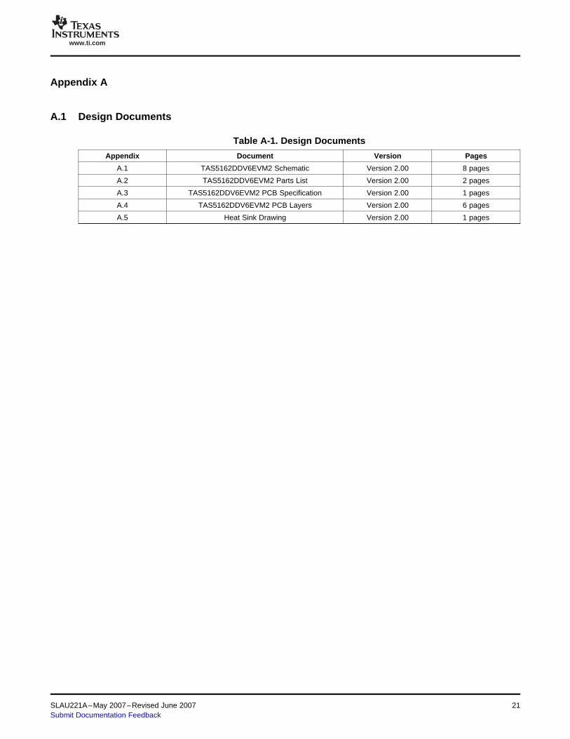
Appendix A
A.1 Design Documents
Table A-1. Design Documents
Appendix Document Version Pages
A.1 TAS5162DDV6EVM2 Schematic Version 2.00 8 pages
A.2 TAS5162DDV6EVM2 Parts List Version 2.00 2 pages
A.3 TAS5162DDV6EVM2 PCB Specification Version 2.00 1 pages
A.4 TAS5162DDV6EVM2 PCB Layers Version 2.00 6 pages
A.5 Heat Sink Drawing Version 2.00 1 pages
SLAU221A–May 2007–Revised June 2007 21Submit Documentation Feedback
5
5
4
4
3
3
2
2
1
1
D D
C C
B B
A A
Rev:
Page Title:
TIHome Audio Amplifiers
ALL RIGHTS RESERVEDTEXAS INSTRUMENTS INCORPORATED
Project:
File Name:
Date:
Engineer:
Page: of
Size:
AUDIO/IMAGING GROUP
A2
2.00
Jonas L. Holm
TAS5162DDV6EVM2 - 3-6 Ch Digital Amplifier Design
A829-SCH-001.DSN
TAS5162DDV6EVM2
Monday, April 30, 2007 1 8
/ Parts List 2.00
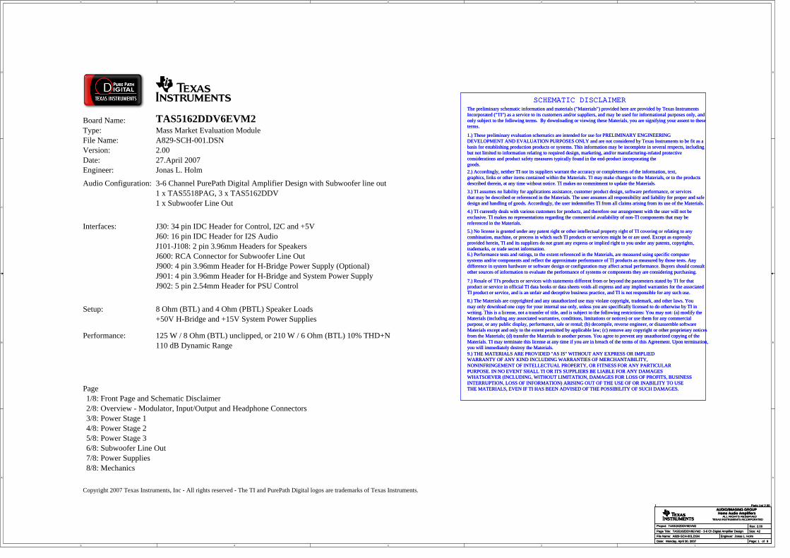
TAS5162DDV6EVM2
Page1/8: Front Page and Schematic Disclaimer2/8: Overview - Modulator, Input/Output and Headphone Connectors3/8: Power Stage 14/8: Power Stage 25/8: Power Stage 36/8: Subwoofer Line Out
Board Name:
Version:Date:Engineer:
Audio Configuration:
Interfaces:
File Name: A829-SCH-001.DSN2.0027.April 2007Jonas L. Holm
3-6 Channel PurePath Digital Amplifier Design with Subwoofer line out1 x TAS5518PAG, 3 x TAS5162DDV
Setup:
Type: Mass Market Evaluation Module
J30: 34 pin IDC Header for Control, I2C and +5VJ60: 16 pin IDC Header for I2S AudioJ101-J108: 2 pin 3.96mm Headers for Speakers
J900: 4 pin 3.96mm Header for H-Bridge Power Supply (Optional)J901: 4 pin 3.96mm Header for H-Bridge and System Power Supply
8 Ohm (BTL) and 4 Ohm (PBTL) Speaker Loads
TI
Copyright 2007 Texas Instruments, Inc - All rights reserved - The TI and PurePath Digital logos are trademarks of Texas Instruments.
J902: 5 pin 2.54mm Header for PSU Control
+50V H-Bridge and +15V System Power Supplies
Performance: 125 W / 8 Ohm (BTL) unclipped, or 210 W / 6 Ohm (BTL) 10% THD+N110 dB Dynamic Range
7/8: Power Supplies8/8: Mechanics
1 x Subwoofer Line Out
J600: RCA Connector for Subwoofer Line Out
SCHEMATIC DISCLAIMERThe preliminary schematic information and materials ("Materials") provided here are provided by Texas Instruments Incorporated ("TI") as a service to its customers and/or suppliers, and may be used for informational purposes only, and only subject to the following terms. By downloading or viewing these Materials, you are signifying your assent to these terms.
1.) These preliminary evaluation schematics are intended for use for PRELIMINARY ENGINEERING DEVELOPMENT AND EVALUATION PURPOSES ONLY and are not considered by Texas Instruments to be fit as a basis for establishing production products or systems. This information may be incomplete in several respects, including but not limited to information relating to required design, marketing, and/or manufacturing-related protective considerations and product safety measures typically found in the end-product incorporating the goods. 2.) Accordingly, neither TI nor its suppliers warrant the accuracy or completeness of the information, text, graphics, links or other items contained within the Materials. TI may make changes to the Materials, or to the products described therein, at any time without notice. TI makes no commitment to update the Materials.
3.) TI assumes no liability for applications assistance, customer product design, software performance, or services that may be described or referenced in the Materials. The user assumes all responsibility and liability for proper and safe design and handling of goods. Accordingly, the user indemnifies TI from all claims arising from its use of the Materials.
4.) TI currently deals with various customers for products, and therefore our arrangement with the user will not be exclusive. TI makes no representations regarding the commercial availability of non-TI components that may be referenced in the Materials.5.) No license is granted under any patent right or other intellectual property right of TI covering or relating to anycombination, machine, or process in which such TI products or services might be or are used. Except as expressly provided herein, TI and its suppliers do not grant any express or implied right to you under any patents, copyrights, trademarks, or trade secret information. 6.) Performance tests and ratings, to the extent referenced in the Materials, are measured using specific computersystems and/or components and reflect the approximate performance of TI products as measured by those tests. Any difference in system hardware or software design or configuration may affect actual performance. Buyers should consult other sources of information to evaluate the performance of systems or components they are considering purchasing.
7.) Resale of TI's products or services with statements different from or beyond the parameters stated by TI for that product or service in official TI data books or data sheets voids all express and any implied warranties for the associated TI product or service, and is an unfair and deceptive business practice, and TI is not responsible for any such use.
8.) The Materials are copyrighted and any unauthorized use may violate copyright, trademark, and other laws. Youmay only download one copy for your internal use only, unless you are specifically licensed to do otherwise by TI inwriting. This is a license, not a transfer of title, and is subject to the following restrictions: You may not: (a) modify the Materials (including any associated warranties, conditions, limitations or notices) or use them for any commercialpurpose, or any public display, performance, sale or rental; (b) decompile, reverse engineer, or disassemble softwareMaterials except and only to the extent permitted by applicable law; (c) remove any copyright or other proprietary notices from the Materials; (d) transfer the Materials to another person. You agree to prevent any unauthorized copying of the Materials. TI may terminate this license at any time if you are in breach of the terms of this Agreement. Upon termination, you will immediately destroy the Materials. 9.) THE MATERIALS ARE PROVIDED "AS IS" WITHOUT ANY EXPRESS OR IMPLIED WARRANTY OF ANY KIND INCLUDING WARRANTIES OF MERCHANTABILITY, NONINFRINGEMENT OF INTELLECTUAL PROPERTY, OR FITNESS FOR ANY PARTICULAR PURPOSE. IN NO EVENT SHALL TI OR ITS SUPPLIERS BE LIABLE FOR ANY DAMAGESWHATSOEVER (INCLUDING, WITHOUT LIMITATION, DAMAGES FOR LOSS OF PROFITS, BUSINESSINTERRUPTION, LOSS OF INFORMATION) ARISING OUT OF THE USE OF OR INABILITY TO USE THE MATERIALS, EVEN IF TI HAS BEEN ADVISED OF THE POSSIBILITY OF SUCH DAMAGES.
5
5
4
4
3
3
2
2
1
1
D D
C C
B B
A A
SDIN1
SDIN2
SDIN3
SCLK
LRCLK
SDA
SCL
VALID
SDIN4
PSVC
/RESET_MODULATOR
/MUTE
/PDN
MCLK
/HP_SEL
VALID
VALID
VALID
/SD
/BKND_ERR/SD
/TW
/SD
/TW
/SD
/TW
/RESET_MODULATOR
/RESET
SDIN1
MCLK
SDIN2
SDIN3
SCLK
LRCLK
SDIN4
PSVC
VDD_SD
VDD_SD
VDD_SD
VDD_SD
/BKND_ERR
/PDN/MUTE/BKND_ERR
/TW
/SD
/RESET
SCL
SDA
/HP_SEL
VALID
GND
+3.3V
GND
GVDD
PVDD
GVDD
+5V
GVDD
+3.3V
GVDD
GND
GND
GND
+5V
PVDD
PVDD
PVDD
AGND
GND
AGND
AGND
GND
+3.3V-AVDD
+3.3V
GND
+3.3V
GND
GND
+3.3V
+3.3V-AVDD
+3.3V +5V
GND
Rev:
Page Title:
TIHome Audio Amplifiers
ALL RIGHTS RESERVEDTEXAS INSTRUMENTS INCORPORATED
Project:
File Name:
Date:
Engineer:
Page: of
Size:
AUDIO/IMAGING GROUP
A2
2.00
Jonas L. Holm
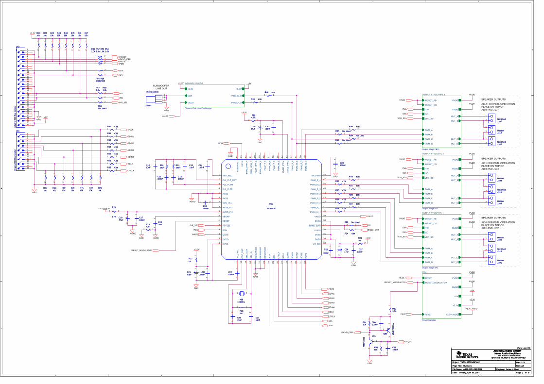
Overview
A829-SCH-001.DSN
TAS5162DDV6EVM2
Monday, April 30, 2007 2 8
/ Parts List 2.00
Rev:
Page Title:
TIHome Audio Amplifiers
ALL RIGHTS RESERVEDTEXAS INSTRUMENTS INCORPORATED
Project:
File Name:
Date:
Engineer:
Page: of
Size:
AUDIO/IMAGING GROUP
A2
2.00
Jonas L. Holm
Overview
A829-SCH-001.DSN
TAS5162DDV6EVM2
Monday, April 30, 2007 2 8
/ Parts List 2.00
Rev:
Page Title:
TIHome Audio Amplifiers
ALL RIGHTS RESERVEDTEXAS INSTRUMENTS INCORPORATED
Project:
File Name:
Date:
Engineer:
Page: of
Size:
AUDIO/IMAGING GROUP
A2
2.00
Jonas L. Holm
Overview
A829-SCH-001.DSN
TAS5162DDV6EVM2
Monday, April 30, 2007 2 8
/ Parts List 2.00
J112 FOR PBTL OPERATIONPLACE ON TOP OFJ108 AND J107
SPEAKER OUTPUTS
J111 FOR PBTL OPERATIONPLACE ON TOP OFJ103 AND J104
SPEAKER OUTPUTS
J110 FOR PBTL OPERATIONPLACE ON TOP OFJ101 AND J102
SPEAKER OUTPUTS
SUBWOOFER LINE OUT
R55200RR55200R
1 2
R26 47RR26 47R1 2
R4410kR4410k
12
R23 Not UsedR23 Not Used12
OUTPUT STAGE BTL 2
Output Stage BTL
PWM_A
PWM_B
PWM_C
PWM_D
OUT_A
OUT_B
GVDD/TW
OUT_C
OUT_D
/SD
/RESET_AB
/RESET_CD
PVDD
VDD_SD
C28100nFC28100nF
21
R4110kR4110k
12
J104HeaderJ104Header
1
2
C2647uFC2647uF
12
R8110kR8110k
12
R4610kR4610k
12
U10
TAS5518
U10
TAS5518
VRA_PLL1
PLL_FLT_RET2
PLL_FLTM3
PLL_FLTP4
AVSS5
AVSS6
VRD_PLL7
AVSS_PLL8
AVDD_PLL9
VBGAP10
RESET11
HP_SEL12
PDN13
MUTE14
DVDD15
DVSS16
VR
_DP
LL17
OS
C_C
AP
18
XTL
_OU
T19
XTL
_IN
20
RE
SE
RV
ED
21
RE
SE
RV
ED
22
RE
SE
RV
ED
23
SD
A24
SC
L25
LRC
LK26
SC
LK27
SD
IN4
28
SD
IN3
29
SD
IN2
30
SD
IN1
31
PS
VC
32
VR_PWM 48
PWM_P_4 47
PWM_M_4 46
PWM_P_3 45
PWM_M_3 44
PWM_P_2 43
PWM_M_2 42
PWM_P_1 41
PWM_M_1 40
VALID 39
DVSS 38
BKND_ERR 37
DVDD 36
DVSS 35
DVSS 34
VR_DIG 33
RE
SE
RV
ED
64
MC
LK63
PW
M_H
PP
_R62
PW
M_H
PM
_R61
PW
M_H
PP
_L60
PW
M_H
PM
_L59
PW
M_P
_658
PW
M_M
_657
PW
M_P
_556
PW
M_M
_555
DV
DD
_PW
M54
DV
SS
_PW
M53
PW
M_P
_852
PW
M_M
_851
PW
M_P
_750
PW
M_M
_749
J111Not UsedJ111Not Used
1
2
C21100nF
C21100nF
21
R50Not UsedR50Not Used
1 2
R521.0kR521.0k
1 2
J40
34 p
ins
IDC
Box
hea
der
J40
34 p
ins
IDC
Box
hea
der
1234567891011
13141516
12
171819202122232425262728293031323334
C2947uFC29
47uF
12
R7110kR7110k
12
R62 47RR62 47R1 2
R15
4.7R
R15
4.7R
1 2
C11100nFC11100nF
21
C30100nFC30
100nF
21
C81100nFC81100nF
21
R27 47RR27 47R1 2
R65 47RR65 47R1 2
C191nFC191nF
21
J600
Phono socket
J600
Phono socket
234
1
C15100nFC15100nF
21
C80100nFC80100nF
21
C14100nFC14100nF
21
C2315pFC2315pF
21
R30 47RR30 47R1 2
C27100nF
C27100nF
21
X1013.5MHz
X1013.5MHz
1 2
R56200RR56200R
1 2
R49 Not UsedR49 Not Used1 2
Subwoofer Line Out
Channel Sub Line Out Design
+3.3V +5.0V
PWM_P_8
PWM_M_8OUT
VALID
R4010kR4010k
12
R48 47RR48 47R1 2
R181MR181M
12
OUTPUT STAGE PBTL 1
Output Stage PBTL
GVDD/TW
/SD
/RESET_AB
/RESET_CD
PWM_D
PWM_C
PWM_B
PWM_A
OUT_A
OUT_B
OUT_C
OUT_D
PVDD
VDD_SD
R8010kR8010k
12
R164.7RR164.7R
1 2
R39 47RR39 47R1 2
R66 47RR66 47R1 2
R531.0kR531.0k
1 2
OUTPUT STAGE BTL 1
Output Stage BTL
PWM_A
PWM_B
PWM_C
PWM_D
OUT_A
OUT_B
GVDD/TW
OUT_C
OUT_D
/SD
/RESET_AB
/RESET_CD
PVDD
VDD_SD
R7010kR7010k
12
R28 47RR28 47R1 2
R24 47RR24 47R
12
Q81
PM
BT2
222
Q81
PM
BT2
222
1
32
J107Not UsedJ107Not Used
1
2
R31 47RR31 47R1 2
R4710kR4710k
12
J110Not UsedJ110Not Used
1
2
J112HeaderJ112Header
1
2
R63 47RR63 47R1 2
R60 47RR60 47R1 2
R571.0kR571.0k1 2
R511.0kR511.0k
1 2
C22100nFC22100nF
21
R36 47RR36 47R1 2
R6710kR6710k
12
R224.7RR224.7R
12
R211RR211R
1 2
C1010nFC1010nF
21
Q80 MM
BT2
907A
Q80 MM
BT2
907A
2
1
3
R35 Not UsedR35 Not Used1 2
R6910kR6910k
12
C12100nFC12100nF
21
J108Not UsedJ108Not Used
1
2
J103HeaderJ103Header
1
2
C25
100nF
C25
100nF
21
C1310nFC1310nF
21
R34 Not UsedR34 Not Used1 2
R541.0kR541.0k
1 2
R32 47RR32 47R1 2
R7310kR7310k
12
R10200RR10200R
12
R171RR171R
12
R29 47RR29 47R1 2
J60
16 p
ins
IDC
Box
hea
der
J60
16 p
ins
IDC
Box
hea
der
1234567891011
13141516
12
R61 47RR61 47R1 2
R4510kR4510k
12
C2047uFC2047uF
12
C1647uFC1647uF
12
J101HeaderJ101Header
1
2
R4210kR4210k
12
R581.0kR581.0k
1 2
R6810kR6810k
12
R11200RR11200R
12
PSU
Power Supplies
/RESET_MODULATOR
+3.3V
GVDD
/RESET
PSVC
PVDD
+5V
+3.3V-AVDD
R8210kR8210k
12
C17100nFC17100nF
21
R64 47RR64 47R1 2
C2415pFC2415pF
21
R4310kR4310k
12
R33 47RR33 47R1 2
R7210kR7210k
12
J102HeaderJ102Header
1
2
5
5
4
4
3
3
2
2
1
1
D D
C C
B B
A A
GVDD
/SD
/TW
/RESET_AB
/RESET_CD
PWM_A
PWM_B
PWM_C
PWM_D
OUT_A
OUT_B
OUT_C
OUT_D
PVDD
VDD_SD
Lx30_2Lx30_1
Lx31_1 Lx31_2
Lx32_2Lx32_1
Lx33_1 Lx33_2
Lx31_1 Lx31_2
Lx30_1 Lx30_2
Lx32_1 Lx32_2
Lx33_1 Lx33_2
GND GND
GND
GND
GND
GND
GND
GNDGND
GND
GND
GND
GND
GND
GND
GND
GND
GND
GND
GND
GND
GND
GND
GND
Rev:
Page Title:
TIHome Audio Amplifiers
ALL RIGHTS RESERVEDTEXAS INSTRUMENTS INCORPORATED
Project:
File Name:
Date:
Engineer:
Page: of
Size:
AUDIO/IMAGING GROUP
A2
2.00
ENGINEER
PAGE TITLE
A829-SCH-001.DSN
PROJECT
Monday, April 30, 2007 3 8
/OUTPUT STAGE BTL 1 Parts List 2.00
Rev:
Page Title:
TIHome Audio Amplifiers
ALL RIGHTS RESERVEDTEXAS INSTRUMENTS INCORPORATED
Project:
File Name:
Date:
Engineer:
Page: of
Size:
AUDIO/IMAGING GROUP
A2
2.00
ENGINEER
PAGE TITLE
A829-SCH-001.DSN
PROJECT
Monday, April 30, 2007 3 8
/OUTPUT STAGE BTL 1 Parts List 2.00
Rev:
Page Title:
TIHome Audio Amplifiers
ALL RIGHTS RESERVEDTEXAS INSTRUMENTS INCORPORATED
Project:
File Name:
Date:
Engineer:
Page: of
Size:
AUDIO/IMAGING GROUP
A2
2.00
ENGINEER
PAGE TITLE
A829-SCH-001.DSN
PROJECT
Monday, April 30, 2007 3 8
/OUTPUT STAGE BTL 1 Parts List 2.00
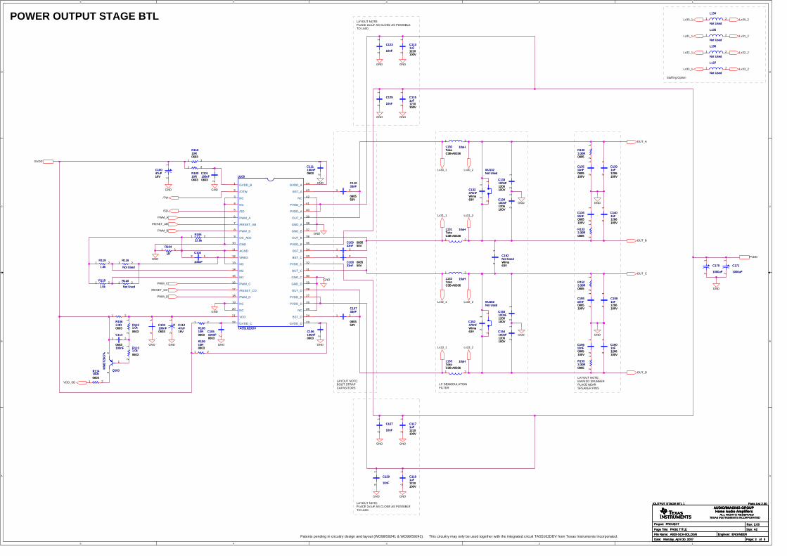
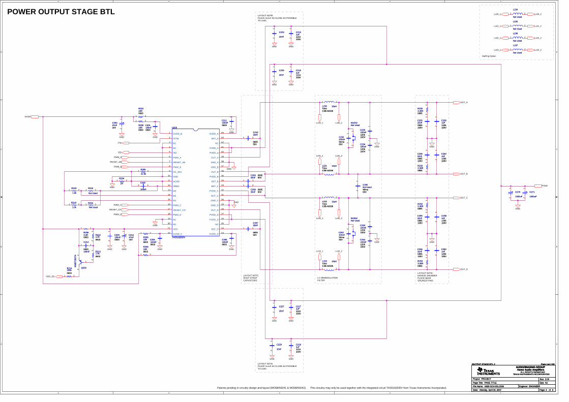
Patents pending in circuitry design and layout (WO99/59241 & WO99/59242). This circuitry may only be used together with the integrated circuit TAS5162DDV from Texas Instruments Incorporated.
POWER OUTPUT STAGE BTL
LAYOUT NOTE:EMI/ESD SNUBBERPLACE NEARSPEAKER PINS
LC DEMODULATIONFILTER
LAYOUT NOTE:BOOT STRAPCAPASITORS
LAYOUT NOTE:PLACE 2x1uF AS CLOSE AS POSSIBLETO Ux00.
LAYOUT NOTE:PLACE 2x1uF AS CLOSE AS POSSIBLETO Ux00.
Stuffing Option
R119
1.0k
R119
1.0k1 2
C106100nF0603
C106100nF0603
21
Q100
MM
BT2
907A
Q100
MM
BT2
907A
2
1
3
R10810R0603
R10810R0603
1 2
C192Not UsedWima63V
C192Not UsedWima63V
21
C125
10nF
C125
10nF21
C1131uF1210100V
C1131uF1210100V
21
C154100nF1206100V
C154100nF1206100V
21
R104
1R
R104
1R1 2
WJ132Not UsedWJ132Not Used
21
L137
Not Used
L137
Not Used1 2
R10910R0603
R10910R0603
1 2
C10733nF
080550V
C10733nF
080550V
21
C132470nFWima63V
C132470nFWima63V
21
C111100nF0603
C111100nF0603 2
1
C1151uF1210100V
C1151uF1210100V
21
C170
1000uF
C170
1000uF
12
WJ152Not UsedWJ152Not Used
21
R1063.3R0603
R1063.3R0603
1 2
C114
100nF0603
C114
100nF0603
21
C129
10nF
C129
10nF21
L131 10uH
C3B-A0336TokoL131 10uH
C3B-A0336Toko
1 2
C1191uF1210100V
C1191uF1210100V
21
R118
1.0k
R118
1.0k1 2
R1533.30R0805
R1533.30R0805
12
C134100nF1206100V
C134100nF1206100V
21
C15510nF0805100V
C15510nF0805100V
21
C102
100nF
C102
100nF
2 1
R1333.30R0805
R1333.30R0805
12
C1401nF1206100V
C1401nF1206100V
21
C1591nF1206100V
C1591nF1206100V
21
L134
Not Used
L134
Not Used1 2
C153100nF1206100V
C153100nF1206100V
21
C10933nF
080550V
C10933nF
080550V
21
C11033nF
080550V
C11033nF
080550V
21
R116
Not Used
R116
Not Used1 2
C1171uF1210100V
C1171uF1210100V
21
L130 10uH
C3B-A0336TokoL130 10uH
C3B-A0336Toko
1 2
C105100nF0603
C105100nF0603
21
U100
TAS5162DDV
U100
TAS5162DDV
NC3
NC4
/SD5
PWM_A6
/RESET_AB7
PWM_B8
OC_ADJ9
GND10
AGND11
VREG12
M313
M214
M115
PWM_C16
/RESET_CD17
PWM_D18
NC19
NC20 NC 25
PVDD_D 26
PVDD_D 27
OUT_D 28
GND_D 29
GND_C 30
OUT_C 31
PVDD_C 32
BST_C 33
BST_B 34
PVDD_B 35
OUT_B 36
GND_B 37
GND_A 38
OUT_A 39
PVDD_A 40
PVDD_A 41
NC 42
GVDD_B1
/OTW2
VDD21
GVDD_C22 GVDD_D 23
BST_D 24
BST_A 43
GVDD_A 44
C15610nF0805100V
C15610nF0805100V
21
C123
10nF
C123
10nF21
L136
Not Used
L136
Not Used1 2
C101100nF0603
C101100nF0603 2
1 C13510nF0805100V
C13510nF0805100V
21
R1523.30R0805
R1523.30R0805
12
C13610nF0805100V
C13610nF0805100V
21
R114100k0603
R114100k0603
1 2
C10833nF
080550V
C10833nF
080550V
21
R1323.30R0805
R1323.30R0805
12
L133 10uH
C3B-A0336TokoL133 10uH
C3B-A0336Toko
1 2
C133100nF1206100V
C133100nF1206100V
21
L132 10uH
C3B-A0336TokoL132 10uH
C3B-A0336Toko
1 2
C104100nF0603
C104100nF06032
1
C1601nF1206100V
C1601nF1206100V
21
C171
1000uF
C171
1000uF
12
R1131.0k0603
R1131.0k0603
12
C11247uF16V
C11247uF16V
12
C1391nF1206100V
C1391nF1206100V
21
C152470nFWima63V
C152470nFWima63V
21
R115
Not Used
R115
Not Used1 2
C127
10nF
C127
10nF21
R10010R0603
R10010R0603
1 2
R105
22.0k
R105
22.0k1 2
C10047uF16V
C10047uF16V
12
R1121.0k0603
R1121.0k0603
12
L135
Not Used
L135
Not Used1 2
R11010R0603
R11010R0603
1 2
5
5
4
4
3
3
2
2
1
1
D D
C C
B B
A A
GVDD
/SD
/TW
/RESET_AB
/RESET_CD
PWM_A
PWM_B
PWM_C
PWM_D
OUT_A
OUT_B
OUT_C
OUT_D
PVDD
VDD_SD
Lx30_2Lx30_1
Lx31_1 Lx31_2
Lx32_2Lx32_1
Lx33_1 Lx33_2
Lx31_1 Lx31_2
Lx30_1 Lx30_2
Lx32_1 Lx32_2
Lx33_1 Lx33_2
GND GND
GND
GND
GND
GND
GND
GNDGND
GND
GND
GND
GND
GND
GND
GND
GND
GND
GND
GND
GND
GND
GND
GND
Rev:
Page Title:
TIHome Audio Amplifiers
ALL RIGHTS RESERVEDTEXAS INSTRUMENTS INCORPORATED
Project:
File Name:
Date:
Engineer:
Page: of
Size:
AUDIO/IMAGING GROUP
A2
2.00
ENGINEER
PAGE TITLE
A829-SCH-001.DSN
PROJECT
Monday, April 30, 2007 4 8
/OUTPUT STAGE BTL 2 Parts List 2.00
Rev:
Page Title:
TIHome Audio Amplifiers
ALL RIGHTS RESERVEDTEXAS INSTRUMENTS INCORPORATED
Project:
File Name:
Date:
Engineer:
Page: of
Size:
AUDIO/IMAGING GROUP
A2
2.00
ENGINEER
PAGE TITLE
A829-SCH-001.DSN
PROJECT
Monday, April 30, 2007 4 8
/OUTPUT STAGE BTL 2 Parts List 2.00
Rev:
Page Title:
TIHome Audio Amplifiers
ALL RIGHTS RESERVEDTEXAS INSTRUMENTS INCORPORATED
Project:
File Name:
Date:
Engineer:
Page: of
Size:
AUDIO/IMAGING GROUP
A2
2.00
ENGINEER
PAGE TITLE
A829-SCH-001.DSN
PROJECT
Monday, April 30, 2007 4 8
/OUTPUT STAGE BTL 2 Parts List 2.00
Patents pending in circuitry design and layout (WO99/59241 & WO99/59242). This circuitry may only be used together with the integrated circuit TAS5162DDV from Texas Instruments Incorporated.
POWER OUTPUT STAGE BTL
LAYOUT NOTE:EMI/ESD SNUBBERPLACE NEARSPEAKER PINS
LC DEMODULATIONFILTER
LAYOUT NOTE:BOOT STRAPCAPASITORS
LAYOUT NOTE:PLACE 2x1uF AS CLOSE AS POSSIBLETO Ux00.
LAYOUT NOTE:PLACE 2x1uF AS CLOSE AS POSSIBLETO Ux00.
Stuffing Option
R219
1.0k
R219
1.0k1 2
C206100nF0603
C206100nF0603
21
Q200
MM
BT2
907A
Q200
MM
BT2
907A
2
1
3
R20810R0603
R20810R0603
1 2
C292Not UsedWima63V
C292Not UsedWima63V
21
C225
10nF
C225
10nF21
C2131uF1210100V
C2131uF1210100V
21
C254100nF1206100V
C254100nF1206100V
21
R204
1R
R204
1R1 2
WJ232Not UsedWJ232Not Used
21
L237
Not Used
L237
Not Used1 2
R20910R0603
R20910R0603
1 2
C20733nF
080550V
C20733nF
080550V
21
C232470nFWima63V
C232470nFWima63V
21
C211100nF0603
C211100nF0603 2
1
C2151uF1210100V
C2151uF1210100V
21
C270
1000uF
C270
1000uF
12
WJ252Not UsedWJ252Not Used
21
R2063.3R0603
R2063.3R0603
1 2
C214
100nF0603
C214
100nF0603
21
C229
10nF
C229
10nF21
L231 10uH
C3B-A0336TokoL231 10uH
C3B-A0336Toko
1 2
C2191uF1210100V
C2191uF1210100V
21
R218
1.0k
R218
1.0k1 2
R2533.30R0805
R2533.30R0805
12
C234100nF1206100V
C234100nF1206100V
21
C25510nF0805100V
C25510nF0805100V
21
C202
100nF
C202
100nF
2 1
R2333.30R0805
R2333.30R0805
12
C2401nF1206100V
C2401nF1206100V
21
C2591nF1206100V
C2591nF1206100V
21
L234
Not Used
L234
Not Used1 2
C253100nF1206100V
C253100nF1206100V
21
C20933nF
080550V
C20933nF
080550V
21
C21033nF
080550V
C21033nF
080550V
21
R216
Not Used
R216
Not Used1 2
C2171uF1210100V
C2171uF1210100V
21
L230 10uH
C3B-A0336TokoL230 10uH
C3B-A0336Toko
1 2
C205100nF0603
C205100nF0603
21
U200
TAS5162DDV
U200
TAS5162DDV
NC3
NC4
/SD5
PWM_A6
/RESET_AB7
PWM_B8
OC_ADJ9
GND10
AGND11
VREG12
M313
M214
M115
PWM_C16
/RESET_CD17
PWM_D18
NC19
NC20 NC 25
PVDD_D 26
PVDD_D 27
OUT_D 28
GND_D 29
GND_C 30
OUT_C 31
PVDD_C 32
BST_C 33
BST_B 34
PVDD_B 35
OUT_B 36
GND_B 37
GND_A 38
OUT_A 39
PVDD_A 40
PVDD_A 41
NC 42
GVDD_B1
/OTW2
VDD21
GVDD_C22 GVDD_D 23
BST_D 24
BST_A 43
GVDD_A 44
C25610nF0805100V
C25610nF0805100V
21
C223
10nF
C223
10nF21
L236
Not Used
L236
Not Used1 2
C201100nF0603
C201100nF0603 2
1 C23510nF0805100V
C23510nF0805100V
21
R2523.30R0805
R2523.30R0805
12
C23610nF0805100V
C23610nF0805100V
21
R214100k0603
R214100k0603
1 2
C20833nF
080550V
C20833nF
080550V
21
R2323.30R0805
R2323.30R0805
12
L233 10uH
C3B-A0336TokoL233 10uH
C3B-A0336Toko
1 2
C233100nF1206100V
C233100nF1206100V
21
L232 10uH
C3B-A0336TokoL232 10uH
C3B-A0336Toko
1 2
C204100nF0603
C204100nF06032
1
C2601nF1206100V
C2601nF1206100V
21
C271
1000uF
C271
1000uF
12
R2131.0k0603
R2131.0k0603
12
C21247uF16V
C21247uF16V
12
C2391nF1206100V
C2391nF1206100V
21
C252470nFWima63V
C252470nFWima63V
21
R215
Not Used
R215
Not Used1 2
C227
10nF
C227
10nF21
R20010R0603
R20010R0603
1 2
R205
22.0k
R205
22.0k1 2
C20047uF16V
C20047uF16V
12
R2121.0k0603
R2121.0k0603
12
L235
Not Used
L235
Not Used1 2
R21010R0603
R21010R0603
1 2
5
5
4
4
3
3
2
2
1
1
D D
C C
B B
A A
GVDD
/SD
/TW
/RESET_AB
/RESET_CD
PWM_A
PWM_B
PWM_C
PWM_D
OUT_A
OUT_B
OUT_C
OUT_D
PVDD
VDD_SD
Lx30_2Lx30_1
Lx31_1 Lx31_2
Lx32_2Lx32_1
Lx33_1 Lx33_2
Lx31_1 Lx31_2
Lx30_1 Lx30_2
Lx32_1 Lx32_2
Lx33_1 Lx33_2
GND GND
GND
GND
GND
GND
GND
GND
GNDGND
GND
GND
GND
GND
GND
GND
GND
GND
GND
GND
GND
GND
GND
GND
Rev:
Page Title:
TIHome Audio Amplifiers
ALL RIGHTS RESERVEDTEXAS INSTRUMENTS INCORPORATED
Project:
File Name:
Date:
Engineer:
Page: of
Size:
AUDIO/IMAGING GROUP
A2
2.00
ENGINEER
PAGE TITLE
A829-SCH-001.DSN
PROJECT
Monday, April 30, 2007 5 8
/OUTPUT STAGE PBTL 1 Parts List 2.00
Rev:
Page Title:
TIHome Audio Amplifiers
ALL RIGHTS RESERVEDTEXAS INSTRUMENTS INCORPORATED
Project:
File Name:
Date:
Engineer:
Page: of
Size:
AUDIO/IMAGING GROUP
A2
2.00
ENGINEER
PAGE TITLE
A829-SCH-001.DSN
PROJECT
Monday, April 30, 2007 5 8
/OUTPUT STAGE PBTL 1 Parts List 2.00
Rev:
Page Title:
TIHome Audio Amplifiers
ALL RIGHTS RESERVEDTEXAS INSTRUMENTS INCORPORATED
Project:
File Name:
Date:
Engineer:
Page: of
Size:
AUDIO/IMAGING GROUP
A2
2.00
ENGINEER
PAGE TITLE
A829-SCH-001.DSN
PROJECT
Monday, April 30, 2007 5 8
/OUTPUT STAGE PBTL 1 Parts List 2.00
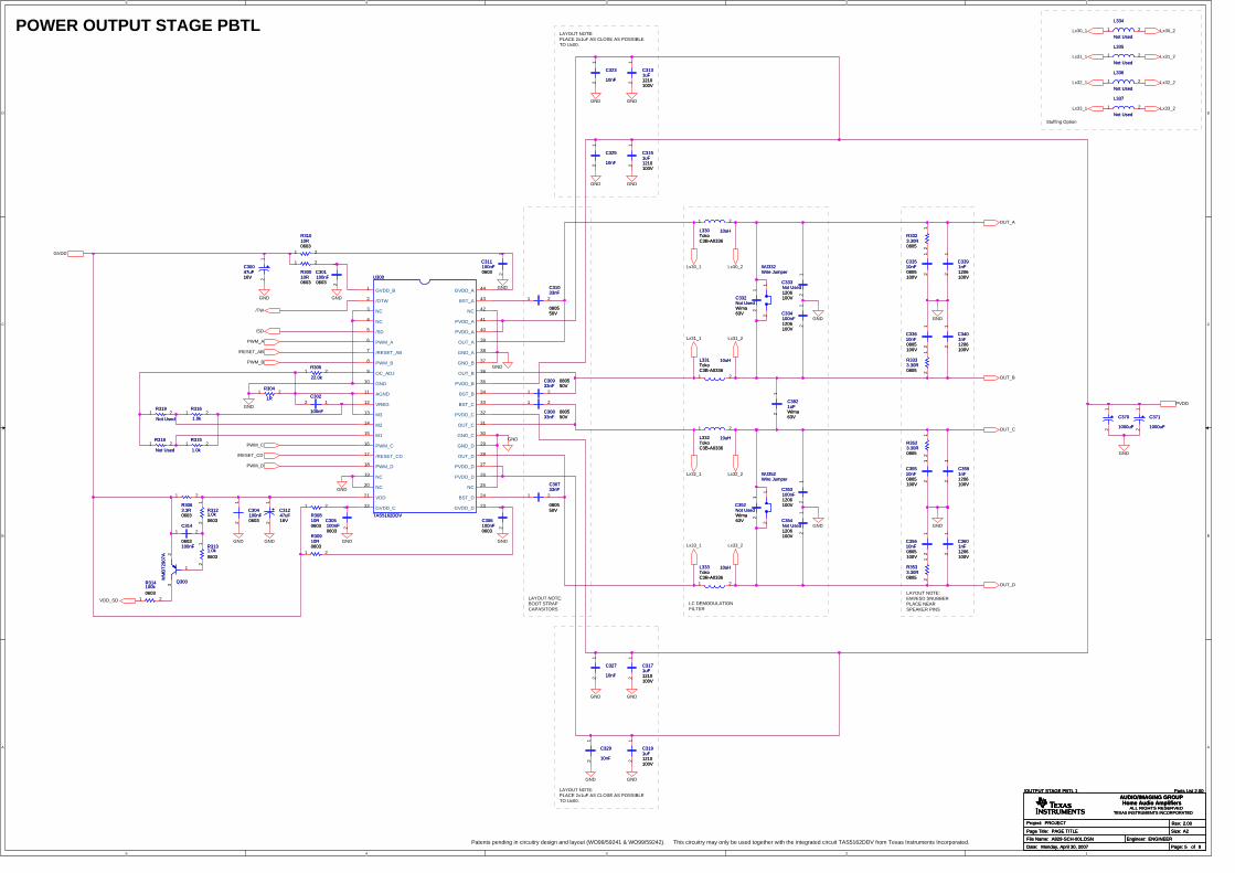
Patents pending in circuitry design and layout (WO99/59241 & WO99/59242). This circuitry may only be used together with the integrated circuit TAS5162DDV from Texas Instruments Incorporated.
POWER OUTPUT STAGE PBTL
LAYOUT NOTE:EMI/ESD SNUBBERPLACE NEARSPEAKER PINS
LC DEMODULATIONFILTER
LAYOUT NOTE:BOOT STRAPCAPASITORS
LAYOUT NOTE:PLACE 2x1uF AS CLOSE AS POSSIBLETO Ux00.
LAYOUT NOTE:PLACE 2x1uF AS CLOSE AS POSSIBLETO Ux00.
Stuffing Option
C352Not UsedWima63V
C352Not UsedWima63V
21
C3401nF1206100V
C3401nF1206100V
21
L333 10uH
C3B-A0336TokoL333 10uH
C3B-A0336Toko
1 2Q300
MM
BT2
907A
Q300
MM
BT2
907A
2
1
3
C304100nF0603
C304100nF06032
1
C354Not Used1206100V
C354Not Used1206100V
21
C302
100nF
C302
100nF
2 1
L335
Not Used
L335
Not Used1 2
C311100nF0603
C311100nF0603 2
1
R31010R0603
R31010R0603
1 2
R3533.30R0805
R3533.30R0805
12
C3151uF1210100V
C3151uF1210100V
21
R318
Not Used
R318
Not Used1 2
C329
10nF
C329
10nF21
C314
100nF0603
C314
100nF0603
21
R305
22.0k
R305
22.0k1 2
R3523.30R0805
R3523.30R0805
12
R316
1.0k
R316
1.0k1 2
R3121.0k0603
R3121.0k0603
12
R3333.30R0805
R3333.30R0805
12
L334
Not Used
L334
Not Used1 2
C333Not Used1206100V
C333Not Used1206100V
21
C305100nF0603
C305100nF0603
21
C3131uF1210100V
C3131uF1210100V
21
R3131.0k0603
R3131.0k0603
12
C3171uF1210100V
C3171uF1210100V
21
R304
1R
R304
1R1 2
R319
Not Used
R319
Not Used1 2
R30010R0603
R30010R0603
1 2
C30733nF
080550V
C30733nF
080550V
21C353100nF1206100V
C353100nF1206100V
21
C30047uF16V
C30047uF16V
12
R30810R0603
R30810R0603
1 2
C370
1000uF
C370
1000uF
12
C332Not UsedWima63V
C332Not UsedWima63V
21
C3191uF1210100V
C3191uF1210100V
21
C30833nF
080550V
C30833nF
080550V
21
C35510nF0805100V
C35510nF0805100V
21
L331 10uH
C3B-A0336TokoL331 10uH
C3B-A0336Toko
1 2
C35610nF0805100V
C35610nF0805100V
21
C371
1000uF
C371
1000uF
12
R30910R0603
R30910R0603
1 2
L337
Not Used
L337
Not Used1 2
C3591nF1206100V
C3591nF1206100V
21
C3391nF1206100V
C3391nF1206100V
21
R314100k0603
R314100k0603
1 2
R3063.3R0603
R3063.3R0603
1 2
WJ332Wire JumperWJ332Wire Jumper
21
C325
10nF
C325
10nF21
C334100nF1206100V
C334100nF1206100V
21
C30933nF
080550V
C30933nF
080550V
21
WJ352Wire JumperWJ352Wire Jumper
21
L332 10uH
C3B-A0336TokoL332 10uH
C3B-A0336Toko
1 2
L330 10uH
C3B-A0336TokoL330 10uH
C3B-A0336Toko
1 2
C31247uF16V
C31247uF16V
12
R315
1.0k
R315
1.0k1 2
C323
10nF
C323
10nF21
C33510nF0805100V
C33510nF0805100V
21
C3601nF1206100V
C3601nF1206100V
21
C327
10nF
C327
10nF21
C301100nF0603
C301100nF0603 2
1
C3921uFWima63V
C3921uFWima63V
21
C306100nF0603
C306100nF0603
21
L336
Not Used
L336
Not Used1 2
U300
TAS5162DDV
U300
TAS5162DDV
NC3
NC4
/SD5
PWM_A6
/RESET_AB7
PWM_B8
OC_ADJ9
GND10
AGND11
VREG12
M313
M214
M115
PWM_C16
/RESET_CD17
PWM_D18
NC19
NC20 NC 25
PVDD_D 26
PVDD_D 27
OUT_D 28
GND_D 29
GND_C 30
OUT_C 31
PVDD_C 32
BST_C 33
BST_B 34
PVDD_B 35
OUT_B 36
GND_B 37
GND_A 38
OUT_A 39
PVDD_A 40
PVDD_A 41
NC 42
GVDD_B1
/OTW2
VDD21
GVDD_C22 GVDD_D 23
BST_D 24
BST_A 43
GVDD_A 44 C31033nF
080550V
C31033nF
080550V
21
R3323.30R0805
R3323.30R0805
12
C33610nF0805100V
C33610nF0805100V
21

5
5
4
4
3
3
2
2
1
1
D D
C C
B B
A A
+3.3V
+5.0V
PWM_P_8
PWM_M_8
VALID
OUT
GND
+5.0V
GND
GND
GND
GND+5.0V
+5.0V
GND
+3.3V
GND
GND
Rev:
Page Title:
TIHome Audio Amplifiers
ALL RIGHTS RESERVEDTEXAS INSTRUMENTS INCORPORATED
Project:
File Name:
Date:
Engineer:
Page: of
Size:
AUDIO/IMAGING GROUP
A2
2.00
Jonas L. Holm
Subwoofer Line Out
A829-SCH-001.DSN
TAS5162DDV6EVM2
Tuesday, May 01, 2007 6 8
/Subwoofer Line Out Parts List 2.00
Rev:
Page Title:
TIHome Audio Amplifiers
ALL RIGHTS RESERVEDTEXAS INSTRUMENTS INCORPORATED
Project:
File Name:
Date:
Engineer:
Page: of
Size:
AUDIO/IMAGING GROUP
A2
2.00
Jonas L. Holm
Subwoofer Line Out
A829-SCH-001.DSN
TAS5162DDV6EVM2
Tuesday, May 01, 2007 6 8
/Subwoofer Line Out Parts List 2.00
Rev:
Page Title:
TIHome Audio Amplifiers
ALL RIGHTS RESERVEDTEXAS INSTRUMENTS INCORPORATED
Project:
File Name:
Date:
Engineer:
Page: of
Size:
AUDIO/IMAGING GROUP
A2
2.00
Jonas L. Holm
Subwoofer Line Out
A829-SCH-001.DSN
TAS5162DDV6EVM2
Tuesday, May 01, 2007 6 8
/Subwoofer Line Out Parts List 2.00
SUBWOOFER LINE OUT
U601
TLV272
U601
TLV272
1OUT1
1IN-2
1IN+3
GND4 2IN+ 5
2IN- 6
2OUT 7
VDD 8
R602
10k
R602
10k
1 2
C606100nFC606100nF
21
C605
220pF
C605
220pF
21
C608100nFC608100nF
21
C603470pFC603470pF
21 R610
100kR610100k
12 C610
10nFC61010nF
21
BU
F
U600
SN74LVC2G126
BU
F
U600
SN74LVC2G126
1OE1
1A2
2Y3
GND4 2A 5
1Y 6
2OE 7
VCC 8
R605
47k
R605
47k
1 2R607
33k
R607
33k
1 2
R606
33k
R606
33k
1 2
C604
220pF
C604
220pF
21
R603
47k
R603
47k
1 2
R611 200RR611 200R1 2
R6081.0kR6081.0k
12
R604
10k
R604
10k
1 2
C60733uFC60733uF
12
C601100nFC601100nF
21
C60933uFC60933uF
1 2
R6091.0kR6091.0k
12
C602470pFC602470pF
21
5
5
4
4
3
3
2
2
1
1
D D
C C
B B
A A
PVDD
/RESET
+5V
GVDD
PSVC/RESET_MODULATOR
+3.3V
+3.3V-AVDD
/RESET_MODULATOR
/RESET
GND
GND
GND GNDGND
GND
GNDGND
GND GND
GND
GND
GND
PVDD
GND GND GND GND GND
GND
GND
GND
GND
GND
GND
GND GND
GND
GND
GND
GND
Rev:
Page Title:
TIHome Audio Amplifiers
ALL RIGHTS RESERVEDTEXAS INSTRUMENTS INCORPORATED
Project:
File Name:
Date:
Engineer:
Page: of
Size:
AUDIO/IMAGING GROUP
A2
2.00
Jonas L. Holm
Power Supplies
A829-SCH-001.DSN
TAS5162DDV6EVM2
Monday, April 30, 2007 7 8
/PSU Parts List 2.00
Rev:
Page Title:
TIHome Audio Amplifiers
ALL RIGHTS RESERVEDTEXAS INSTRUMENTS INCORPORATED
Project:
File Name:
Date:
Engineer:
Page: of
Size:
AUDIO/IMAGING GROUP
A2
2.00
Jonas L. Holm
Power Supplies
A829-SCH-001.DSN
TAS5162DDV6EVM2
Monday, April 30, 2007 7 8
/PSU Parts List 2.00
Rev:
Page Title:
TIHome Audio Amplifiers
ALL RIGHTS RESERVEDTEXAS INSTRUMENTS INCORPORATED
Project:
File Name:
Date:
Engineer:
Page: of
Size:
AUDIO/IMAGING GROUP
A2
2.00
Jonas L. Holm
Power Supplies
A829-SCH-001.DSN
TAS5162DDV6EVM2
Monday, April 30, 2007 7 8
/PSU Parts List 2.00
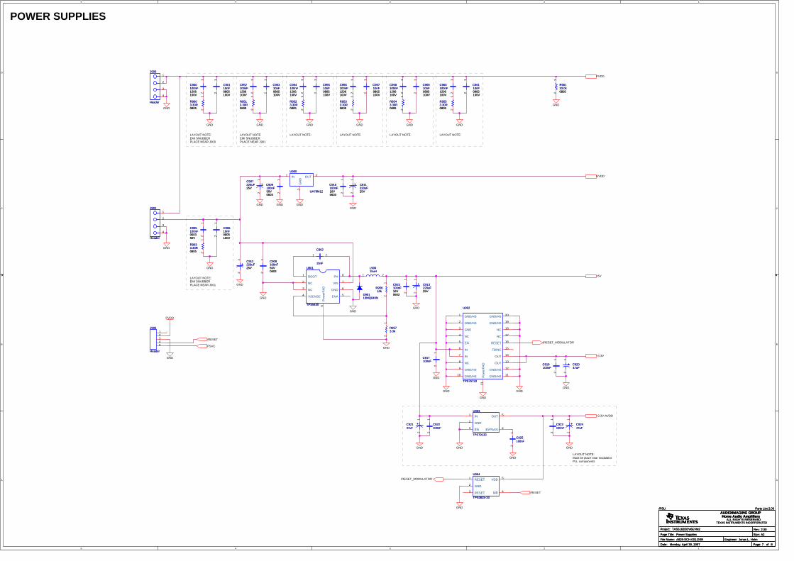
POWER SUPPLIES
LAYOUT NOTE:EMI SNUBBERPLACE NEAR J900
LAYOUT NOTE:EMI SNUBBERPLACE NEAR J901
LAYOUT NOTE:EMI SNUBBERPLACE NEAR J901
LAYOUT NOTE: LAYOUT NOTE: LAYOUT NOTE: LAYOUT NOTE:
LAYOUT NOTE:Must be place near modulatorPLL components
C913220uF25V
C913220uF25V
12
C917100nFC917100nF
21
L90015uHL90015uH
1 2
U904
TPS3825-33
U904
TPS3825-33
RESET1
GND2
RESET3 MR 4
VDD 5
C912220uF25V
C912220uF25V
12
J900
Header
J900
Header
1
2
3
4
C956100nF1206100V
C956100nF1206100V
21
C900100nF1206100V
C900100nF1206100V
21
C95710nF0805100V
C95710nF0805100V
21
R9573.3kR9573.3k
12
D90110MQ040ND90110MQ040N
J901
Header
J901
Header
1
2
3
4
C95910nF0805100V
C95910nF0805100V
21
C911220uF25V
C911220uF25V
12
J902
Header
J902
Header
12345
U901
TPS5430
U901
TPS5430
BOOT1
NC2
NC3
VSENSE4 ENA 5
GND 6
VIN 7
PH 8
Pow
erP
AD
9
R95610k
R95610k
12
R9543.30R0805
R9543.30R0805
12
C958100nF1206100V
C958100nF1206100V
21
U902
TPS76733
U902
TPS76733
GND/HS1
GND/HS2
GND3
NC4
EN5
IN6
IN7
NC8
GND/HS9
GND/HS10 GND/HS 11
GND/HS 12
OUT 13
OUT 14
GND/HS 20
GND/HS 19
NC 18
NC 17
RESET 16
FB/NC 15
Pow
erP
AD
21
C954100nF1206100V
C954100nF1206100V
21
C962
10nF
C962
10nF
21
C96110nF0805100V
C96110nF0805100V
21
R9033.30R0805
R9033.30R0805
12
R9523.30R0805
R9523.30R0805
12
C919100nFC919100nF
21
C960100nF1206100V
C960100nF1206100V
21
C92147uFC92147uF
12
C92447uFC92447uF
12
C90110nF0805100V
C90110nF0805100V
21
R90133.0k0805
R90133.0k0805
12
C95510nF0805100V
C95510nF0805100V
21
C910100nF16V0603
C910100nF16V0603
21
C915100nF16V0603
C915100nF16V0603
21
R9553.30R0805
R9553.30R0805
12
C907220uF25V
C907220uF25V
12
C908100nF50V0603
C908100nF50V06032
1
U903
TPS79133
U903
TPS79133
IN1
GND2
EN3 BYPASS 4
OUT 5
C922100nFC922100nF
21
R9513.30R0805
R9513.30R0805
12
R9003.30R0805
R9003.30R0805
12
C95310nF0805100V
C95310nF0805100V
21
C905100nF060350V
C905100nF060350V
21
C952100nF1206100V
C952100nF1206100V
21
U900
UA78M12
U900
UA78M12
IN1 OUT 3
GN
D2
R9533.30R0805
R9533.30R0805
12
C923100nFC923100nF
21
C925100nFC925100nF
21
C90610nF0805100V
C90610nF0805100V
21
C92047uFC92047uF
12
C909100nF50V0603
C909100nF50V0603
21
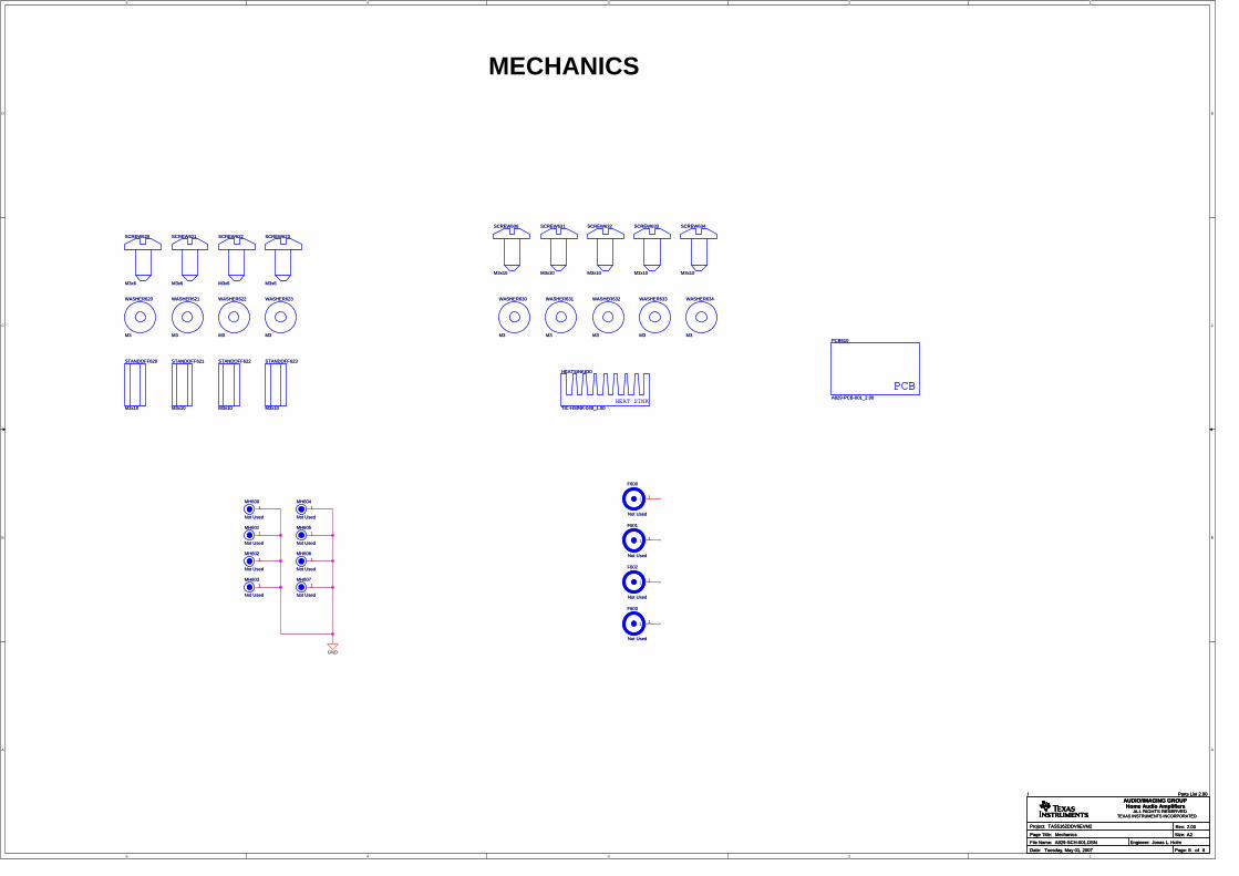
5
5
4
4
3
3
2
2
1
1
D D
C C
B B
A A
GND
Rev:
Page Title:
TIHome Audio Amplifiers
ALL RIGHTS RESERVEDTEXAS INSTRUMENTS INCORPORATED
Project:
File Name:
Date:
Engineer:
Page: of
Size:
AUDIO/IMAGING GROUP
A2
2.00
Jonas L. Holm
Mechanics
A829-SCH-001.DSN
TAS5162DDV6EVM2
Tuesday, May 01, 2007 8 8
/ Parts List 2.00
Rev:
Page Title:
TIHome Audio Amplifiers
ALL RIGHTS RESERVEDTEXAS INSTRUMENTS INCORPORATED
Project:
File Name:
Date:
Engineer:
Page: of
Size:
AUDIO/IMAGING GROUP
A2
2.00
Jonas L. Holm
Mechanics
A829-SCH-001.DSN
TAS5162DDV6EVM2
Tuesday, May 01, 2007 8 8
/ Parts List 2.00
Rev:
Page Title:
TIHome Audio Amplifiers
ALL RIGHTS RESERVEDTEXAS INSTRUMENTS INCORPORATED
Project:
File Name:
Date:
Engineer:
Page: of
Size:
AUDIO/IMAGING GROUP
A2
2.00
Jonas L. Holm
Mechanics
A829-SCH-001.DSN
TAS5162DDV6EVM2
Tuesday, May 01, 2007 8 8
/ Parts List 2.00
MECHANICS
STANDOFF623
M3x10
STANDOFF623
M3x10
WASHER634
M3
WASHER634
M3
STANDOFF621
M3x10
STANDOFF621
M3x10
WASHER620
M3
WASHER620
M3
SCREW633
M3x10
SCREW633
M3x10
MH603
Not Used
MH603
Not Used
1
STANDOFF620
M3x10
STANDOFF620
M3x10
F602
Not Used
F602
Not Used
1 1
WASHER633
M3
WASHER633
M3
PCB
PCB610
A829-PCB-001_2.00
PCB
PCB610
A829-PCB-001_2.00
SCREW622
M3x6
SCREW622
M3x6
MH600
Not Used
MH600
Not Used
1
STANDOFF622
M3x10
STANDOFF622
M3x10
F600
Not Used
F600
Not Used
1 1
MH602
Not Used
MH602
Not Used
1
F601
Not Used
F601
Not Used
1 1
WASHER623
M3
WASHER623
M3
SCREW632
M3x10
SCREW632
M3x10
MH606
Not Used
MH606
Not Used
1
SCREW631
M3x10
SCREW631
M3x10
F603
Not Used
F603
Not Used
1 1
WASHER630
M3
WASHER630
M3
MH601
Not Used
MH601
Not Used
1
SCREW634
M3x10
SCREW634
M3x10
HEAT SINK
HEATSINK630
TIC-HSINK-048_1.00HEAT SINK
HEATSINK630
TIC-HSINK-048_1.00
SCREW630
M3x10
SCREW630
M3x10
SCREW620
M3x6
SCREW620
M3x6
MH605
Not Used
MH605
Not Used
1
SCREW623
M3x6
SCREW623
M3x6
MH604
Not Used
MH604
Not Used
1
WASHER632
M3
WASHER632
M3
WASHER622
M3
WASHER622
M3
WASHER621
M3
WASHER621
M3
WASHER631
M3
WASHER631
M3
SCREW621
M3x6
SCREW621
M3x6
MH607
Not Used
MH607
Not Used
1
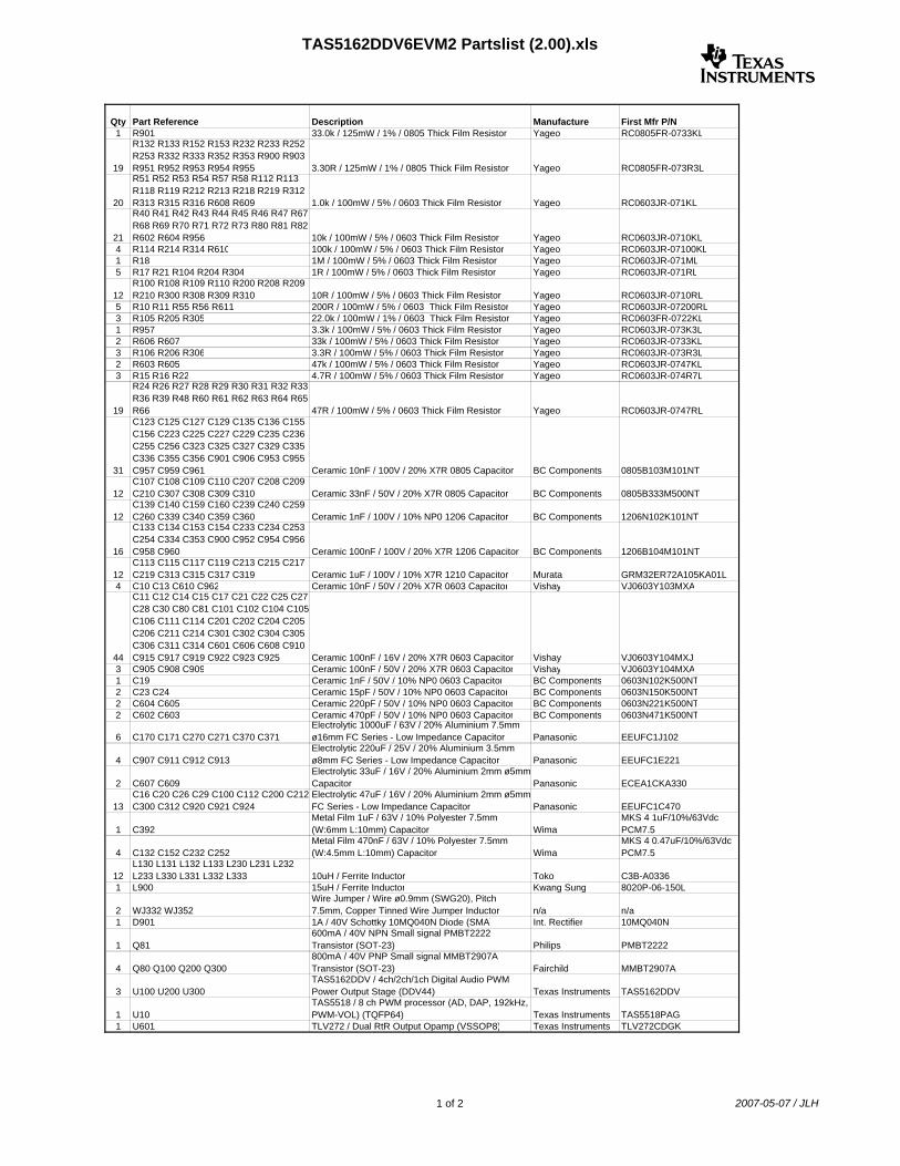
TAS5162DDV6EVM2 Partslist (2.00).xls
tiQty Part Reference Description Manufacture First Mfr P/N
1 R901 33.0k / 125mW / 1% / 0805 Thick Film Resistor Yageo RC0805FR-0733KL
19
R132 R133 R152 R153 R232 R233 R252 R253 R332 R333 R352 R353 R900 R903 R951 R952 R953 R954 R955 3.30R / 125mW / 1% / 0805 Thick Film Resistor Yageo RC0805FR-073R3L
20
R51 R52 R53 R54 R57 R58 R112 R113 R118 R119 R212 R213 R218 R219 R312 R313 R315 R316 R608 R609 1.0k / 100mW / 5% / 0603 Thick Film Resistor Yageo RC0603JR-071KL
21
R40 R41 R42 R43 R44 R45 R46 R47 R67 R68 R69 R70 R71 R72 R73 R80 R81 R82 R602 R604 R956 10k / 100mW / 5% / 0603 Thick Film Resistor Yageo RC0603JR-0710KL
4 R114 R214 R314 R610 100k / 100mW / 5% / 0603 Thick Film Resistor Yageo RC0603JR-07100KL1 R18 1M / 100mW / 5% / 0603 Thick Film Resistor Yageo RC0603JR-071ML5 R17 R21 R104 R204 R304 1R / 100mW / 5% / 0603 Thick Film Resistor Yageo RC0603JR-071RL
12R100 R108 R109 R110 R200 R208 R209 R210 R300 R308 R309 R310 10R / 100mW / 5% / 0603 Thick Film Resistor Yageo RC0603JR-0710RL
5 R10 R11 R55 R56 R611 200R / 100mW / 5% / 0603 Thick Film Resistor Yageo RC0603JR-07200RL3 R105 R205 R305 22.0k / 100mW / 1% / 0603 Thick Film Resistor Yageo RC0603FR-0722KL1 R957 3.3k / 100mW / 5% / 0603 Thick Film Resistor Yageo RC0603JR-073K3L2 R606 R607 33k / 100mW / 5% / 0603 Thick Film Resistor Yageo RC0603JR-0733KL3 R106 R206 R306 3.3R / 100mW / 5% / 0603 Thick Film Resistor Yageo RC0603JR-073R3L2 R603 R605 47k / 100mW / 5% / 0603 Thick Film Resistor Yageo RC0603JR-0747KL3 R15 R16 R22 4.7R / 100mW / 5% / 0603 Thick Film Resistor Yageo RC0603JR-074R7L
19
R24 R26 R27 R28 R29 R30 R31 R32 R33 R36 R39 R48 R60 R61 R62 R63 R64 R65 R66 47R / 100mW / 5% / 0603 Thick Film Resistor Yageo RC0603JR-0747RL
31
C123 C125 C127 C129 C135 C136 C155 C156 C223 C225 C227 C229 C235 C236 C255 C256 C323 C325 C327 C329 C335 C336 C355 C356 C901 C906 C953 C955 C957 C959 C961 Ceramic 10nF / 100V / 20% X7R 0805 Capacitor BC Components 0805B103M101NT
12C107 C108 C109 C110 C207 C208 C209 C210 C307 C308 C309 C310 Ceramic 33nF / 50V / 20% X7R 0805 Capacitor BC Components 0805B333M500NT
12C139 C140 C159 C160 C239 C240 C259 C260 C339 C340 C359 C360 Ceramic 1nF / 100V / 10% NP0 1206 Capacitor BC Components 1206N102K101NT
16
C133 C134 C153 C154 C233 C234 C253 C254 C334 C353 C900 C952 C954 C956 C958 C960 Ceramic 100nF / 100V / 20% X7R 1206 Capacitor BC Components 1206B104M101NT
12C113 C115 C117 C119 C213 C215 C217 C219 C313 C315 C317 C319 Ceramic 1uF / 100V / 10% X7R 1210 Capacitor Murata GRM32ER72A105KA01L
4 C10 C13 C610 C962 Ceramic 10nF / 50V / 20% X7R 0603 Capacitor Vishay VJ0603Y103MXA
44
C11 C12 C14 C15 C17 C21 C22 C25 C27 C28 C30 C80 C81 C101 C102 C104 C105 C106 C111 C114 C201 C202 C204 C205 C206 C211 C214 C301 C302 C304 C305 C306 C311 C314 C601 C606 C608 C910 C915 C917 C919 C922 C923 C925 Ceramic 100nF / 16V / 20% X7R 0603 Capacitor Vishay VJ0603Y104MXJ
3 C905 C908 C909 Ceramic 100nF / 50V / 20% X7R 0603 Capacitor Vishay VJ0603Y104MXA1 C19 Ceramic 1nF / 50V / 10% NP0 0603 Capacitor BC Components 0603N102K500NT2 C23 C24 Ceramic 15pF / 50V / 10% NP0 0603 Capacitor BC Components 0603N150K500NT2 C604 C605 Ceramic 220pF / 50V / 10% NP0 0603 Capacitor BC Components 0603N221K500NT2 C602 C603 Ceramic 470pF / 50V / 10% NP0 0603 Capacitor BC Components 0603N471K500NT
6 C170 C171 C270 C271 C370 C371Electrolytic 1000uF / 63V / 20% Aluminium 7.5mm ø16mm FC Series - Low Impedance Capacitor Panasonic EEUFC1J102
4 C907 C911 C912 C913Electrolytic 220uF / 25V / 20% Aluminium 3.5mm ø8mm FC Series - Low Impedance Capacitor Panasonic EEUFC1E221
2 C607 C609Electrolytic 33uF / 16V / 20% Aluminium 2mm ø5mmCapacitor Panasonic ECEA1CKA330
13C16 C20 C26 C29 C100 C112 C200 C212 C300 C312 C920 C921 C924
Electrolytic 47uF / 16V / 20% Aluminium 2mm ø5mmFC Series - Low Impedance Capacitor Panasonic EEUFC1C470
1 C392Metal Film 1uF / 63V / 10% Polyester 7.5mm (W:6mm L:10mm) Capacitor Wima
MKS 4 1uF/10%/63Vdc PCM7.5
4 C132 C152 C232 C252Metal Film 470nF / 63V / 10% Polyester 7.5mm (W:4.5mm L:10mm) Capacitor Wima
MKS 4 0.47uF/10%/63Vdc PCM7.5
12L130 L131 L132 L133 L230 L231 L232 L233 L330 L331 L332 L333 10uH / Ferrite Inductor Toko C3B-A0336
1 L900 15uH / Ferrite Inductor Kwang Sung 8020P-06-150L
2 WJ332 WJ352Wire Jumper / Wire ø0.9mm (SWG20), Pitch 7.5mm, Copper Tinned Wire Jumper Inductor n/a n/a
1 D901 1A / 40V Schottky 10MQ040N Diode (SMA) Int. Rectifier 10MQ040N
1 Q81600mA / 40V NPN Small signal PMBT2222 Transistor (SOT-23) Philips PMBT2222
4 Q80 Q100 Q200 Q300800mA / 40V PNP Small signal MMBT2907A Transistor (SOT-23) Fairchild MMBT2907A
3 U100 U200 U300TAS5162DDV / 4ch/2ch/1ch Digital Audio PWM Power Output Stage (DDV44) Texas Instruments TAS5162DDV
1 U10TAS5518 / 8 ch PWM processor (AD, DAP, 192kHz, PWM-VOL) (TQFP64) Texas Instruments TAS5518PAG
1 U601 TLV272 / Dual RtR Output Opamp (VSSOP8) Texas Instruments TLV272CDGK
1 of 2 2007-05-07 / JLH
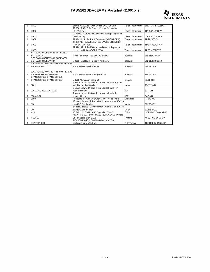
TAS5162DDV6EVM2 Partslist (2.00).xls
ti1 U600 SN74LVC2G126 / Dual Buffer, LVC (SSOP8) Texas Instruments SN74LVC2G126DCT
1 U904TPS3825-33 / 3.3V Supply Voltage Supervisor (SOP5-DBV) Texas Instruments TPS3825-33DBVT
1 U900UA78M12 / 12V/500mA Positive Voltage Regulator (PFM2-KTP) Texas Instruments UA78M12CKTPR
1 U901 TPS5430 / 5V/3A Buck Converter (HSOP8-DDA) Texas Instruments TPS5430DDA
1 U902TPS76733 / 3.3V/1A Low Drop Voltage Regulator (HTSSOP20-PWP) Texas Instruments TPS76733QPWP
1 U903TPS79133 / 3.3V/100mA Low Dropout Regulator (Ultra Low Noise) (SOP5-DBV) Texas Instruments TPS79133DBVR
4SCREW620 SCREW621 SCREW622 SCREW623 M3x6 Pan Head, Pozidriv, A2 Screw Bossard BN 81882 M3x6
5SCREW630 SCREW631 SCREW632 SCREW633 SCREW634 M3x10 Pan Head, Pozidriv, A2 Screw Bossard BN 81882 M3x10
4WASHER620 WASHER621 WASHER622 WASHER623 M3 Stainless Steel Washer Bossard BN 670 M3
5WASHER630 WASHER631 WASHER632 WASHER633 WASHER634 M3 Stainless Steel Spring Washer Bossard BN 760 M3
4STANDOFF620 STANDOFF621 STANDOFF622 STANDOFF623 M3x10 Aluminium Stand-off Ettinger 05.03.108
1 J9025 pins / 1 row / 2.54mm Pitch Vertical Male Friction lock Pin header Header Molex 22-27-2051
5 J101 J102 J103 J104 J1122 pins / 1 row / 3.96mm Pitch Vertical Male Pin header Header JST B2P-VH
2 J900 J9014 pins / 1 row / 3.96mm Pitch Vertical Male Pin header Header JST B4P-VH
1 J600 Horizontal Female w. Switch Coax Phono socke Chunfeng RJ843-4W
1 J6016 pins / 2 rows / 2.54mm Pitch Vertical Male IDC 16pins IDC Box header Molex 87256-1611
1 J4034 pins / 2 rows / 2.54mm Pitch Vertical Male IDC 34pins IDC Box header Molex 87256-3411
1 X10 13.5MHz 13.5MHz SMD Crystal (HCM49) Citizen HCM49-13.500MABJT
1 PCB610A829-PCB-001_2.00 / TAS5162DDV6EVM2 Printed Circuit Board (ver. 2.00) Printline A829-PCB-001(2.00)
1 HEATSINK630TIC-HSINK-048_2.00 / Heatsink for 3 DDV packages length 154mm THF-Teknik TIC-HSINK-048(2.00)
2 of 2 2007-05-07 / JLH
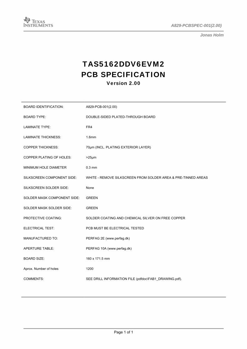
TI A829-PCBSPEC-001(2.00)
Jonas Holm
Page 1 of 1
TAS5162DDV6EVM2 PCB SPECIFICATION
Version 2.00
BOARD IDENTIFICATION: A829-PCB-001(2.00)
BOARD TYPE: DOUBLE-SIDED PLATED-THROUGH BOARD
LAMINATE TYPE: FR4
LAMINATE THICKNESS: 1.6mm
COPPER THICKNESS: 70μm (INCL. PLATING EXTERIOR LAYER)
COPPER PLATING OF HOLES: >25μm
MINIMUM HOLE DIAMETER 0.3 mm
SILKSCREEN COMPONENT SIDE: WHITE - REMOVE SILKSCREEN FROM SOLDER AREA & PRE-TINNED AREAS
SILKSCREEN SOLDER SIDE: None
SOLDER MASK COMPONENT SIDE: GREEN
SOLDER MASK SOLDER SIDE: GREEN
PROTECTIVE COATING: SOLDER COATING AND CHEMICAL SILVER ON FREE COPPER
ELECTRICAL TEST: PCB MUST BE ELECTRICAL TESTED
MANUFACTURED TO: PERFAG 2E (www.perfag.dk)
APERTURE TABLE: PERFAG 10A (www.perfag.dk)
BOARD SIZE: 160 x 171.5 mm
Aprox. Number of holes 1200
COMMENTS: SEE DRILL INFORMATION FILE (pdfdoc\FAB1_DRAWING.pdf).
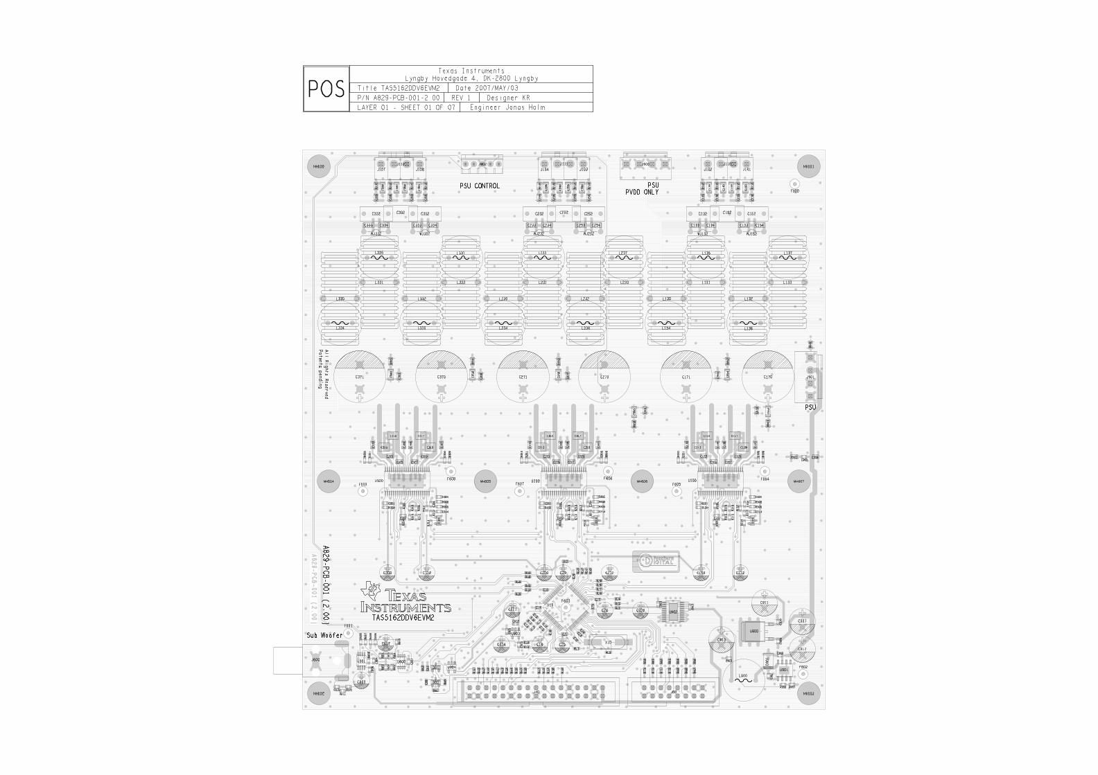
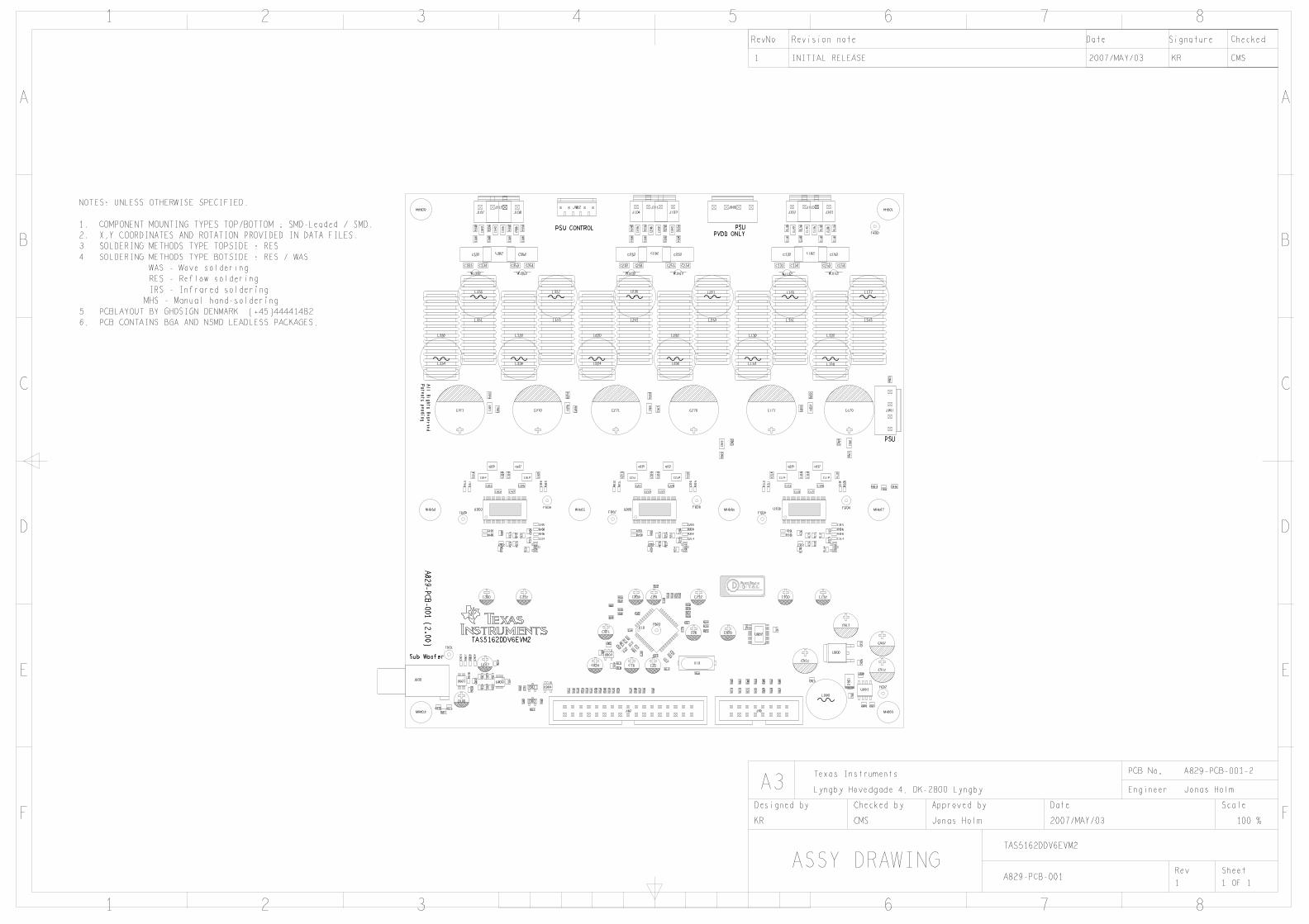
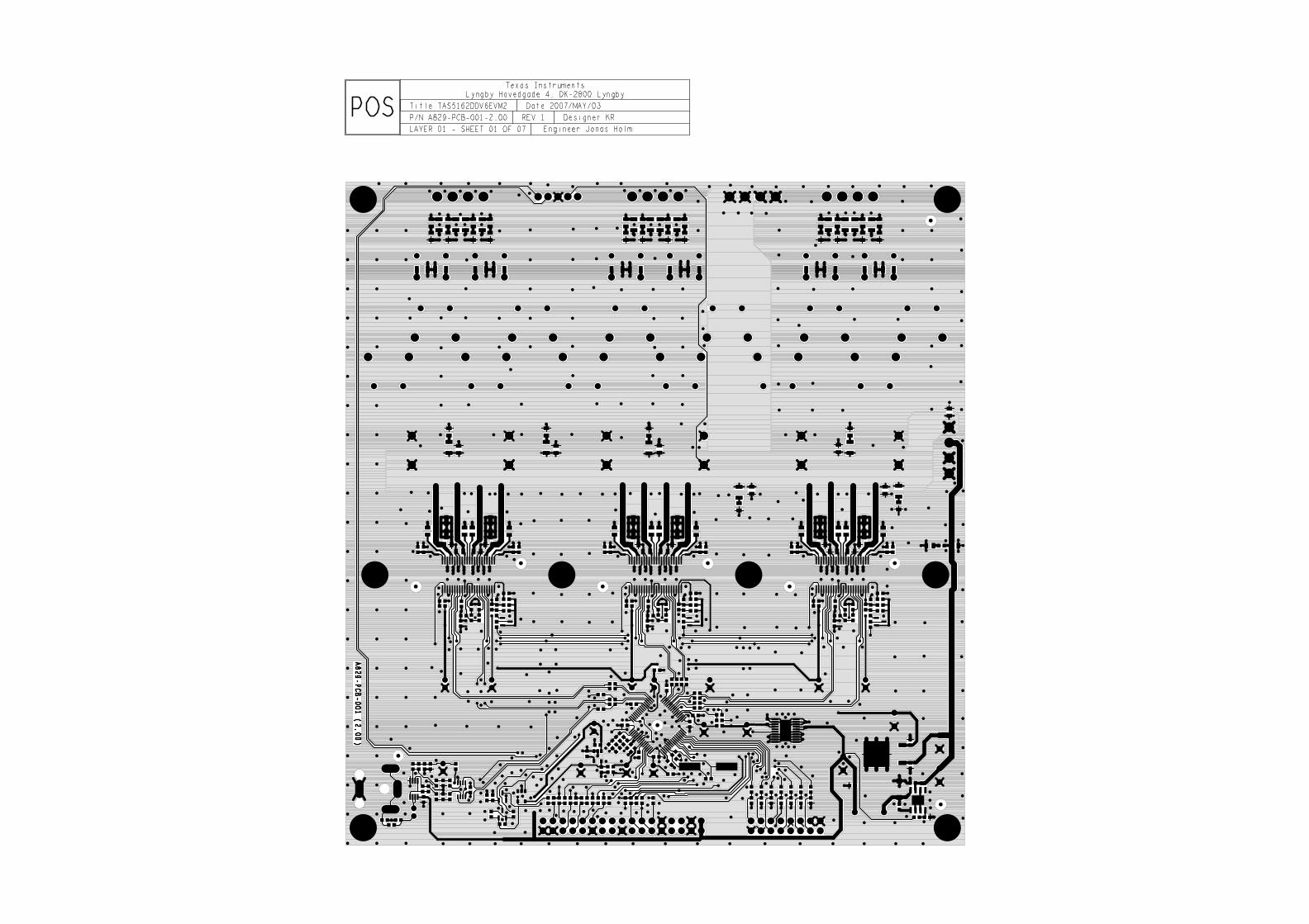
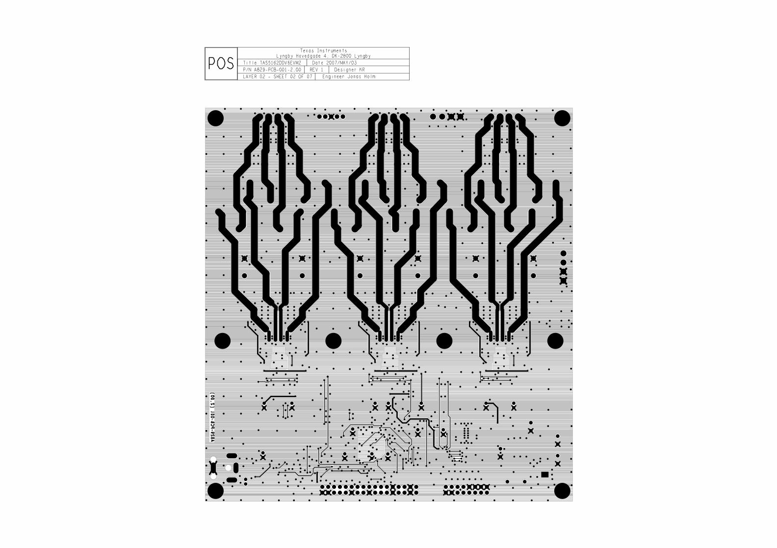
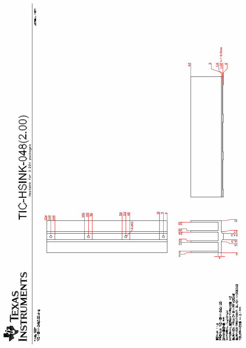
EVALUATION BOARD/KIT IMPORTANT NOTICE
Texas Instruments (TI) provides the enclosed product(s) under the following conditions:
This evaluation board/kit is intended for use for ENGINEERING DEVELOPMENT, DEMONSTRATION, OR EVALUATIONPURPOSES ONLY and is not considered by TI to be a finished end-product fit for general consumer use. Persons handling theproduct(s) must have electronics training and observe good engineering practice standards. As such, the goods being provided arenot intended to be complete in terms of required design-, marketing-, and/or manufacturing-related protective considerations,including product safety and environmental measures typically found in end products that incorporate such semiconductorcomponents or circuit boards. This evaluation board/kit does not fall within the scope of the European Union directives regardingelectromagnetic compatibility, restricted substances (RoHS), recycling (WEEE), FCC, CE or UL, and therefore may not meet thetechnical requirements of these directives or other related directives.
Should this evaluation board/kit not meet the specifications indicated in the User’s Guide, the board/kit may be returned within 30days from the date of delivery for a full refund. THE FOREGOING WARRANTY IS THE EXCLUSIVE WARRANTY MADE BYSELLER TO BUYER AND IS IN LIEU OF ALL OTHER WARRANTIES, EXPRESSED, IMPLIED, OR STATUTORY, INCLUDINGANY WARRANTY OF MERCHANTABILITY OR FITNESS FOR ANY PARTICULAR PURPOSE.
The user assumes all responsibility and liability for proper and safe handling of the goods. Further, the user indemnifies TI from allclaims arising from the handling or use of the goods. Due to the open construction of the product, it is the user’s responsibility totake any and all appropriate precautions with regard to electrostatic discharge.
EXCEPT TO THE EXTENT OF THE INDEMNITY SET FORTH ABOVE, NEITHER PARTY SHALL BE LIABLE TO THE OTHERFOR ANY INDIRECT, SPECIAL, INCIDENTAL, OR CONSEQUENTIAL DAMAGES.
TI currently deals with a variety of customers for products, and therefore our arrangement with the user is not exclusive.
TI assumes no liability for applications assistance, customer product design, software performance, or infringement ofpatents or services described herein.
Please read the User’s Guide and, specifically, the Warnings and Restrictions notice in the User’s Guide prior to handling theproduct. This notice contains important safety information about temperatures and voltages. For additional information on TI’senvironmental and/or safety programs, please contact the TI application engineer or visit www.ti.com/esh.
No license is granted under any patent right or other intellectual property right of TI covering or relating to any machine, process, orcombination in which such TI products or services might be or are used.
FCC Warning
This evaluation board/kit is intended for use for ENGINEERING DEVELOPMENT, DEMONSTRATION, OR EVALUATIONPURPOSES ONLY and is not considered by TI to be a finished end-product fit for general consumer use. It generates, uses, andcan radiate radio frequency energy and has not been tested for compliance with the limits of computing devices pursuant to part 15of FCC rules, which are designed to provide reasonable protection against radio frequency interference. Operation of thisequipment in other environments may cause interference with radio communications, in which case the user at his own expensewill be required to take whatever measures may be required to correct this interference.
Mailing Address: Texas Instruments, Post Office Box 655303, Dallas, Texas 75265Copyright © 2007, Texas Instruments Incorporated
EVM WARNINGS AND RESTRICTIONS
It is important to operate this EVM within the input voltage range of 3.3 V to 5 V and the output voltage range of 0 V to 5 V.
Exceeding the specified input range may cause unexpected operation and/or irreversible damage to the EVM. If there arequestions concerning the input range, please contact a TI field representative prior to connecting the input power.
Applying loads outside of the specified output range may result in unintended operation and/or possible permanent damage to theEVM. Please consult the EVM User's Guide prior to connecting any load to the EVM output. If there is uncertainty as to the loadspecification, please contact a TI field representative.
During normal operation, some circuit components may have case temperatures greater than 30°C. The EVM is designed tooperate properly with certain components above 85°C as long as the input and output ranges are maintained. These componentsinclude but are not limited to linear regulators, switching transistors, pass transistors, and current sense resistors. These types ofdevices can be identified using the EVM schematic located in the EVM User's Guide. When placing measurement probes nearthese devices during operation, please be aware that these devices may be very warm to the touch.
Mailing Address: Texas Instruments, Post Office Box 655303, Dallas, Texas 75265Copyright © 2007, Texas Instruments Incorporated
IMPORTANT NOTICE
Texas Instruments Incorporated and its subsidiaries (TI) reserve the right to make corrections, modifications, enhancements,improvements, and other changes to its products and services at any time and to discontinue any product or service without notice.Customers should obtain the latest relevant information before placing orders and should verify that such information is current andcomplete. All products are sold subject to TI’s terms and conditions of sale supplied at the time of order acknowledgment.
TI warrants performance of its hardware products to the specifications applicable at the time of sale in accordance with TI’sstandard warranty. Testing and other quality control techniques are used to the extent TI deems necessary to support thiswarranty. Except where mandated by government requirements, testing of all parameters of each product is not necessarilyperformed.
TI assumes no liability for applications assistance or customer product design. Customers are responsible for their products andapplications using TI components. To minimize the risks associated with customer products and applications, customers shouldprovide adequate design and operating safeguards.
TI does not warrant or represent that any license, either express or implied, is granted under any TI patent right, copyright, maskwork right, or other TI intellectual property right relating to any combination, machine, or process in which TI products or servicesare used. Information published by TI regarding third-party products or services does not constitute a license from TI to use suchproducts or services or a warranty or endorsement thereof. Use of such information may require a license from a third party underthe patents or other intellectual property of the third party, or a license from TI under the patents or other intellectual property of TI.
Reproduction of TI information in TI data books or data sheets is permissible only if reproduction is without alteration and isaccompanied by all associated warranties, conditions, limitations, and notices. Reproduction of this information with alteration is anunfair and deceptive business practice. TI is not responsible or liable for such altered documentation. Information of third partiesmay be subject to additional restrictions.
Resale of TI products or services with statements different from or beyond the parameters stated by TI for that product or servicevoids all express and any implied warranties for the associated TI product or service and is an unfair and deceptive businesspractice. TI is not responsible or liable for any such statements.
TI products are not authorized for use in safety-critical applications (such as life support) where a failure of the TI product wouldreasonably be expected to cause severe personal injury or death, unless officers of the parties have executed an agreementspecifically governing such use. Buyers represent that they have all necessary expertise in the safety and regulatory ramificationsof their applications, and acknowledge and agree that they are solely responsible for all legal, regulatory and safety-relatedrequirements concerning their products and any use of TI products in such safety-critical applications, notwithstanding anyapplications-related information or support that may be provided by TI. Further, Buyers must fully indemnify TI and itsrepresentatives against any damages arising out of the use of TI products in such safety-critical applications.
TI products are neither designed nor intended for use in military/aerospace applications or environments unless the TI products arespecifically designated by TI as military-grade or "enhanced plastic." Only products designated by TI as military-grade meet militaryspecifications. Buyers acknowledge and agree that any such use of TI products which TI has not designated as military-grade issolely at the Buyer's risk, and that they are solely responsible for compliance with all legal and regulatory requirements inconnection with such use.
TI products are neither designed nor intended for use in automotive applications or environments unless the specific TI productsare designated by TI as compliant with ISO/TS 16949 requirements. Buyers acknowledge and agree that, if they use anynon-designated products in automotive applications, TI will not be responsible for any failure to meet such requirements.
Following are URLs where you can obtain information on other Texas Instruments products and application solutions:
Products Applications
Amplifiers amplifier.ti.com Audio www.ti.com/audio
Data Converters dataconverter.ti.com Automotive www.ti.com/automotive
DSP dsp.ti.com Broadband www.ti.com/broadband
Interface interface.ti.com Digital Control www.ti.com/digitalcontrol
Logic logic.ti.com Military www.ti.com/military
Power Mgmt power.ti.com Optical Networking www.ti.com/opticalnetwork
Microcontrollers microcontroller.ti.com Security www.ti.com/security
RFID www.ti-rfid.com Telephony www.ti.com/telephony
Low Power www.ti.com/lpw Video & Imaging www.ti.com/videoWireless
Wireless www.ti.com/wireless
Mailing Address: Texas Instruments, Post Office Box 655303, Dallas, Texas 75265Copyright © 2007, Texas Instruments Incorporated