Embed Size (px)
Citation preview
TB-FMCL-USB30 Hardware User Manual
1 Rev.1.00
TB-FMCL-USB30 Hardware User Manual
Rev.1.00
TB-FMCL-USB30 Hardware User Manual
2 Rev.1.00
Revision History Version Date Description Publisher
Rev.1.00 2012/06/19 Initial Release Yoshioka
TB-FMCL-USB30 Hardware User Manual
3 Rev.1.00
Table of Contents 1. Related Documents and Accessories ......................................................................................... 8 2. Overview ...................................................................................................................................... 8 3. Feature ........................................................................................................................................ 8 4. Block Diagram ............................................................................................................................. 9 5. External View of the Board ........................................................................................................ 10 6. Board Specifications ................................................................................................................... 11 7. Description of Components ....................................................................................................... 12
7.1. Power supply ........................................................................................................................... 12 7.1.1. Power supply circuit structure .......................................................................................... 12 7.1.2. VBUS power supply circuit .............................................................................................. 12 7.1.3. FMC power supply circuit ................................................................................................ 13
7.2. FMC connector for platform board (J1) ................................................................................... 14 7.3. USB3.0 TYPE-B connector (CN1) ........................................................................................... 19 7.4. I2S Pin Header (CN2) .............................................................................................................. 19 7.5. SPI Pin Header (CN5) and SPI Flash (U9) ............................................................................. 20 7.6. I2C Pin Header (CN6) ............................................................................................................. 21 7.7. RS-232 Pin Header (CN7) ....................................................................................................... 22 7.8. LEDs and Push Switch ............................................................................................................ 23
7.8.1. LED(D1, D3, D4 and D6) ................................................................................................. 23 7.8.2. Push Switch (SW1) .......................................................................................................... 23
7.9. Jumper ..................................................................................................................................... 24 7.9.1. PMODE (JP2-4) ............................................................................................................... 24 7.9.2. IFSEL (JP5-8) .................................................................................................................. 24 7.9.3. CLK (JP11) ...................................................................................................................... 25
8. Default Settings ......................................................................................................................... 26
TB-FMCL-USB30 Hardware User Manual
4 Rev.1.00
List of Figures
Figure 4-1 Block Diagram .................................................................................................................. 9 Figure 5-1 Component Side ............................................................................................................. 10 Figure 5-2 Solder Side ..................................................................................................................... 10 Figure 6-1 Board Dimension (Top) .................................................................................................... 11 Figure 6-2 Board Dimension (Bottom) .............................................................................................. 11 Figure 7-1 Power Supply Circuit Structure ....................................................................................... 12 Figure 7-2 VBUS power supply circuit ............................................................................................. 12 Figure 7-3 FMC power supply circuit ............................................................................................... 13 Figure 7-4 FMC Connector Standard Pin Assign ............................................................................. 14 Figure 7-5 USB3.0 TYPE-B Connector ............................................................................................ 19 Figure 7-6 I2S Pin header ................................................................................................................ 19 Figure 7-7 SPI Pin header (CN5) ..................................................................................................... 20 Figure 7-8 SPI Flash Memory (U9) .................................................................................................. 20 Figure 7-9 I2C pin header (CN6) ...................................................................................................... 21 Figure 7-10 RS-232C Transceiver (U10) and pin header (CN7) ..................................................... 22 Figure 7-11 Push Switch (SW1) ....................................................................................................... 23 Figure 7-12 PMODE jumper (JP2-4) ................................................................................................ 24 Figure 7-13 IFSEL (JP5-8) ............................................................................................................... 24 Figure 7-14 Clock Select (JP11) ...................................................................................................... 25 Figure 8-1 Default Settings .............................................................................................................. 26
List of Tables Table 7-1 FMC pin assign - Colum C - ............................................................................................. 15 Table 7-2 FMC pin assign - Colum D - ............................................................................................. 16 Table 7-3 FMC pin assign - Colum G - ............................................................................................. 17 Table 7-4 FMC pin assign - Colum H - ............................................................................................. 18 Table 7-5 I2S Pin header connector ................................................................................................. 19 Table 7-6 SPI pin header assign ...................................................................................................... 20 Table 7-7 I2C pin header for external devices ................................................................................. 21 Table 7-8 I2C access from FPGA ..................................................................................................... 21 Table 7-9 RS-232C pin header (CN7) .............................................................................................. 22 Table 7-10 LED Status...................................................................................................................... 23 Table 7-11 PMODE setting (JP2-4) .................................................................................................. 24 Table 7-12 IFSEL (JP5-8) ................................................................................................................. 24 Table 7-13 Clock Select (JP11) ........................................................................................................ 25 Table 8-1 Default Settings ................................................................................................................ 26
TB-FMCL-USB30 Hardware User Manual
5 Rev.1.00
Introduction Thank you for purchasing the TB-FMCL-USB30 board. Before using the product, be sure to carefully read this user manual and fully understand how to correctly use the product. First read through this manual, then always keep it handy.
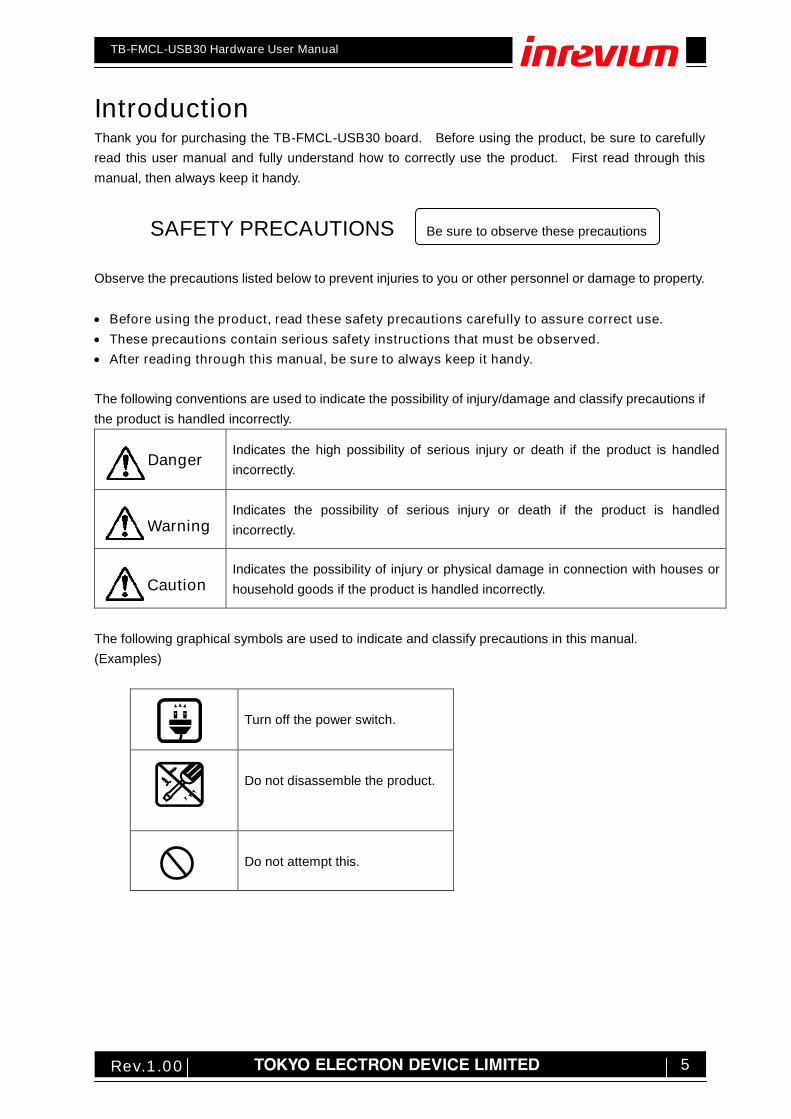
SAFETY PRECAUTIONS Be sure to observe these precautions Observe the precautions listed below to prevent injuries to you or other personnel or damage to property. Before using the product, read these safety precautions carefully to assure correct use. These precautions contain serious safety instructions that must be observed. After reading through this manual, be sure to always keep it handy. The following conventions are used to indicate the possibility of injury/damage and classify precautions if the product is handled incorrectly.
Indicates the high possibility of serious injury or death if the product is handled incorrectly.
Indicates the possibility of serious injury or death if the product is handled incorrectly.
Indicates the possibility of injury or physical damage in connection with houses or household goods if the product is handled incorrectly.
The following graphical symbols are used to indicate and classify precautions in this manual. (Examples)
Turn off the power switch.
Do not disassemble the product.
Do not attempt this.
Danger
Warning
Caution
!

TB-FMCL-USB30 Hardware User Manual
6 Rev.1.00
In the event of a failure, disconnect the power supply. If the product is used as is, a fire or electric shock may occur. Disconnect the power supply immediately and contact our sales personnel for repair.
If an unpleasant smell or smoking occurs, disconnect the power supply. If the product is used as is, a fire or electric shock may occur. Disconnect the power supply immediately. After verifying that no smoking is observed, contact our sales personnel for repair.
Do not disassemble, repair or modify the product. Otherwise, a fire or electric shock may occur due to a short circuit or heat generation. For inspection, modification or repair, contact our sales personnel.
Do not touch a cooling fan. As a cooling fan rotates in high speed, do not put your hand close to it. Otherwise, it may cause injury to persons. Never touch a rotating cooling fan.
Do not place the product on unstable locations. Otherwise, it may drop or fall, resulting in injury to persons or failure.
If the product is dropped or damaged, do not use it as is. Otherwise, a fire or electric shock may occur.
Do not touch the product with a metallic object. Otherwise, a fire or electric shock may occur.
Do not place the product in dusty or humid locations or where water may
splash. Otherwise, a fire or electric shock may occur.
Do not get the product wet or touch it with a wet hand. Otherwise, the product may break down or it may cause a fire, smoking or electric shock.
Do not touch a connector on the product (gold-plated portion). Otherwise, the surface of a connector may be contaminated with sweat or skin oil, resulting in contact failure of a connector or it may cause a malfunction, fire or electric shock due to static electricity.
Warning
!
!
!
!
!
!
!
TB-FMCL-USB30 Hardware User Manual
7 Rev.1.00
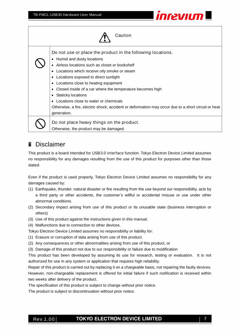
Do not use or place the product in the following locations. Humid and dusty locations Airless locations such as closet or bookshelf Locations which receive oily smoke or steam Locations exposed to direct sunlight Locations close to heating equipment Closed inside of a car where the temperature becomes high Staticky locations Locations close to water or chemicals Otherwise, a fire, electric shock, accident or deformation may occur due to a short circuit or heat generation.
Do not place heavy things on the product. Otherwise, the product may be damaged.
■ Disclaimer This product is a board intended for USB3.0 interface function. Tokyo Electron Device Limited assumes no responsibility for any damages resulting from the use of this product for purposes other than those stated. Even if the product is used properly, Tokyo Electron Device Limited assumes no responsibility for any damages caused by: (1) Earthquake, thunder, natural disaster or fire resulting from the use beyond our responsibility, acts by
a third party or other accidents, the customer’s willful or accidental misuse or use under other abnormal conditions.
(2) Secondary impact arising from use of this product or its unusable state (business interruption or others)
(3) Use of this product against the instructions given in this manual. (4) Malfunctions due to connection to other devices. Tokyo Electron Device Limited assumes no responsibility or liability for: (1) Erasure or corruption of data arising from use of this product. (2) Any consequences or other abnormalities arising from use of this product, or (3) Damage of this product not due to our responsibility or failure due to modification This product has been developed by assuming its use for research, testing or evaluation. It is not authorized for use in any system or application that requires high reliability. Repair of this product is carried out by replacing it on a chargeable basis, not repairing the faulty devices. However, non-chargeable replacement is offered for initial failure if such notification is received within two weeks after delivery of the product. The specification of this product is subject to change without prior notice. The product is subject to discontinuation without prior notice.
Caution
!
!
TB-FMCL-USB30 Hardware User Manual
8 Rev.1.00
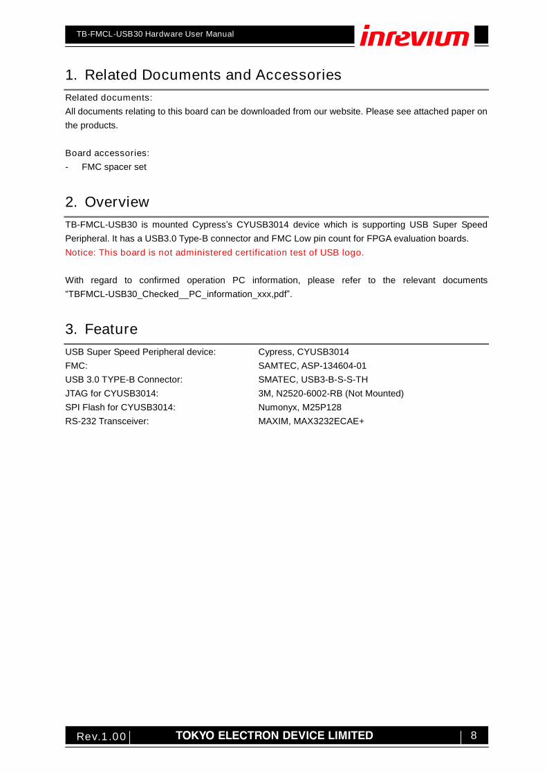
1. Related Documents and Accessories Related documents: All documents relating to this board can be downloaded from our website. Please see attached paper on the products. Board accessories: - FMC spacer set
2. Overview TB-FMCL-USB30 is mounted Cypress’s CYUSB3014 device which is supporting USB Super Speed Peripheral. It has a USB3.0 Type-B connector and FMC Low pin count for FPGA evaluation boards. Notice: This board is not administered certification test of USB logo. With regard to confirmed operation PC information, please refer to the relevant documents “TBFMCL-USB30_Checked__PC_information_xxx,pdf”.
3. Feature USB Super Speed Peripheral device: Cypress, CYUSB3014 FMC: SAMTEC, ASP-134604-01 USB 3.0 TYPE-B Connector: SMATEC, USB3-B-S-S-TH JTAG for CYUSB3014: 3M, N2520-6002-RB (Not Mounted) SPI Flash for CYUSB3014: Numonyx, M25P128 RS-232 Transceiver: MAXIM, MAX3232ECAE+
TB-FMCL-USB30 Hardware User Manual
9 Rev.1.00
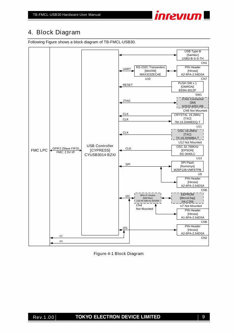
4. Block Diagram Following Figure shows a block diagram of TB-FMCL-USB30.
USB Controller[CYPRESS]
CYUSB3014-BZXI
PIN Header[Hirose]
A2-5PA-2.54DSA
UART RS-232C Transeviers[MAXIM]
MAX3232ECAEU10 CN7
PUSH SW x 1[OMRON]
B3SN-3012PSW1
RESET
SPI Flash[Numonyx]
M25P128-VMF6TPBU9
SPI
JTAG Connector[3M]
N2520-6002-RB
JTAG
CN8 Not Mounted
OSC 32.768KHz[EPSON]
SG-3040LC
CLK
U13
EEPROM[MicroChip]24LC256
I2C
CN4Not Mounted
8Pin IC Socket[Mill-Max]
110-44-308-41-001000
OSC 19.2MHz[TXC]
7X-19.200MBA-T
CLK
U12 Not Mounted
CRYSTAL 19.2MHz[TXC]
7M-19.200MEEQ-T
CLK
U11
CLK
U7 Not Mounted
FMC LPC
PIN Header[Hirose]
A2-6PA-2.54DSACN5
CN2
I2S PIN Header[Hirose]
A2-6PA-2.54DSA
GPIF2 (Slave FIFO)
USB Type-B[Samtec]
USB3-B-S-S-THCN1
FMC: 2.5V I/F
PIN Header[Hirose]
A1-6PA-2.54DSACN6
I2C
I2S
Figure 4-1 Block Diagram
TB-FMCL-USB30 Hardware User Manual
10 Rev.1.00
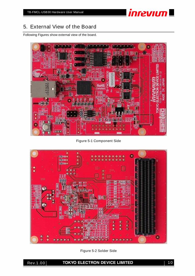
5. External View of the Board Following Figures show external view of the board.
Figure 5-1 Component Side
Figure 5-2 Solder Side
TB-FMCL-USB30 Hardware User Manual
11 Rev.1.00
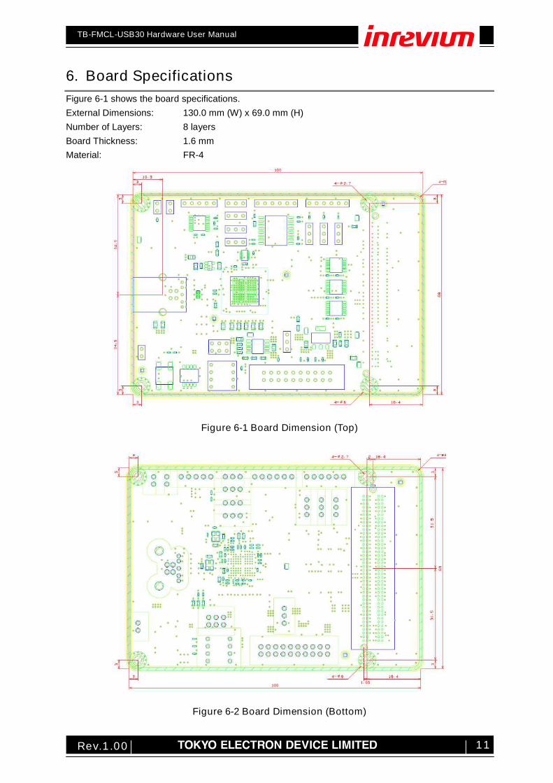
6. Board Specifications Figure 6-1 shows the board specifications. External Dimensions: 130.0 mm (W) x 69.0 mm (H) Number of Layers: 8 layers Board Thickness: 1.6 mm Material: FR-4
Figure 6-1 Board Dimension (Top)
Figure 6-2 Board Dimension (Bottom)
TB-FMCL-USB30 Hardware User Manual
12 Rev.1.00
7. Description of Components 7.1. Power supply 7.1.1. Power supply circuit structure Following figure shows internal power supply circuit.
VCC_5P0VVBUS
VCC_3P3V
VCC_1P2V
3P3V
VCC_2P5V
CYUSB3014VBUS
CYUSB3014SPI,UART,OSC,etc...
CYUSB3014
CYUSB3014EEPROM,etc...
200mA
80mA
400mA
60mA60mA
120mA
USBCN
FMCCN
OVP
FB
LDO3.3V->1.2V(TPS76801QD)
LDO3.3V->2.5V
(RT9183-25PGF)
Figure 7-1 Power Supply Circuit Structure
7.1.2. VBUS power supply circuit VBUS power is provided from USB connector.
Figure 7-2 VBUS power supply circuit
TB-FMCL-USB30 Hardware User Manual
13 Rev.1.00
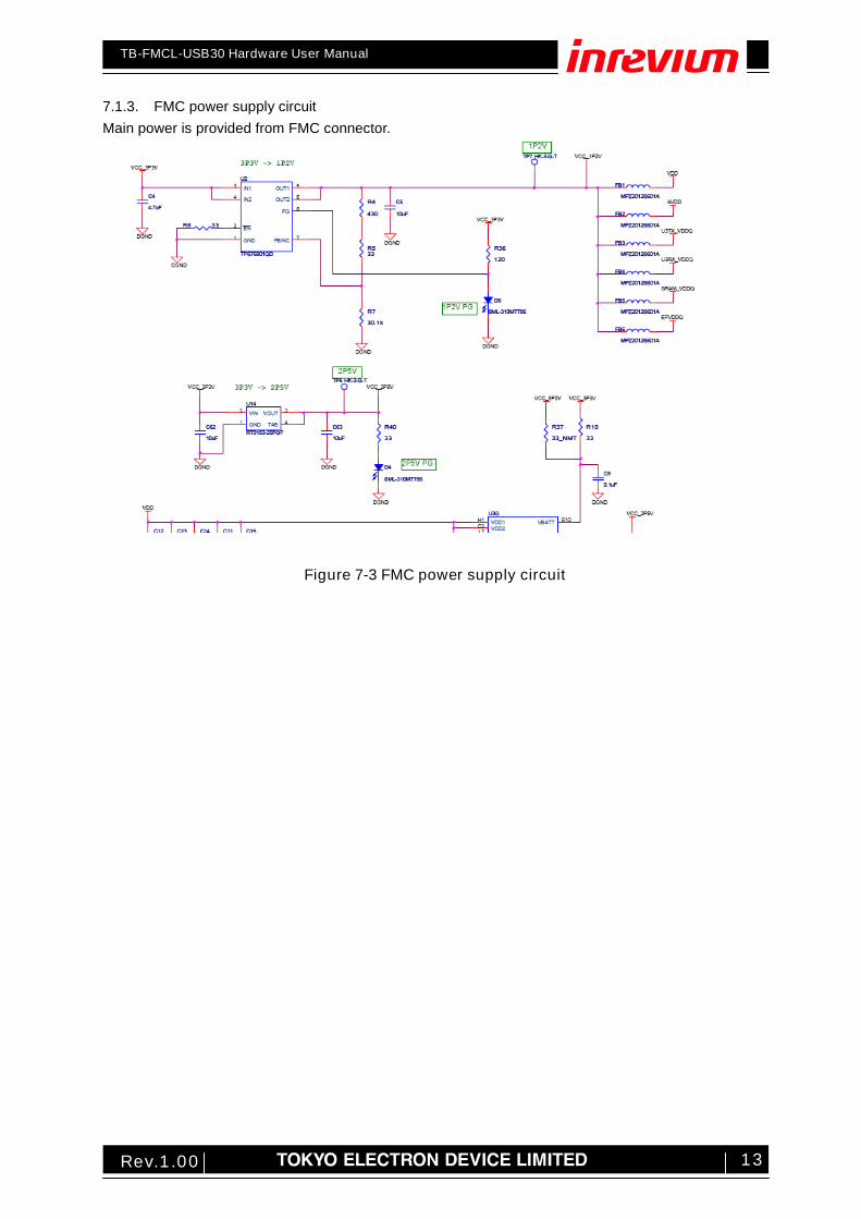
7.1.3. FMC power supply circuit Main power is provided from FMC connector.
Figure 7-3 FMC power supply circuit
TB-FMCL-USB30 Hardware User Manual
14 Rev.1.00
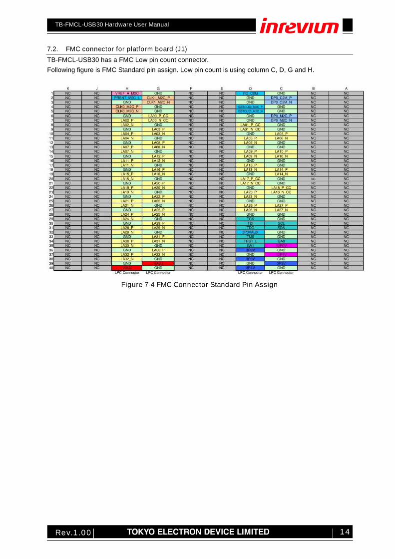
7.2. FMC connector for platform board (J1) TB-FMCL-USB30 has a FMC Low pin count connector. Following figure is FMC Standard pin assign. Low pin count is using column C, D, G and H.
Figure 7-4 FMC Connector Standard Pin Assign
TB-FMCL-USB30 Hardware User Manual
15 Rev.1.00
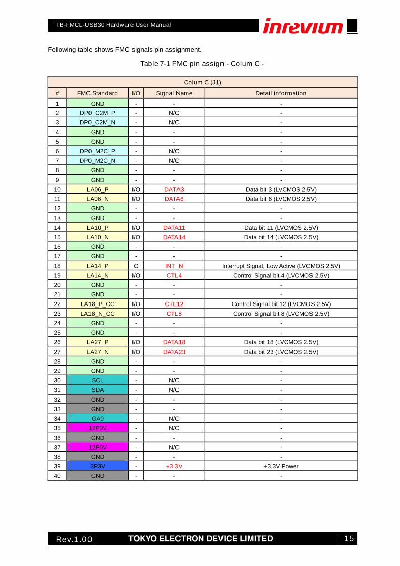
Following table shows FMC signals pin assignment.
Table 7-1 FMC pin assign - Colum C -
Colum C (J1)
# FMC Standard I/O Signal Name Detail information
1 GND - - - 2 DP0_C2M_P - N/C - 3 DP0_C2M_N - N/C - 4 GND - - - 5 GND - - - 6 DP0_M2C_P - N/C - 7 DP0_M2C_N - N/C - 8 GND - - - 9 GND - - -
10 LA06_P I/O DATA3 Data bit 3 (LVCMOS 2.5V) 11 LA06_N I/O DATA6 Data bit 6 (LVCMOS 2.5V) 12 GND - - - 13 GND - - - 14 LA10_P I/O DATA11 Data bit 11 (LVCMOS 2.5V) 15 LA10_N I/O DATA14 Data bit 14 (LVCMOS 2.5V) 16 GND - - - 17 GND - - - 18 LA14_P O INT_N Interrupt Signal, Low Active (LVCMOS 2.5V) 19 LA14_N I/O CTL4 Control Signal bit 4 (LVCMOS 2.5V) 20 GND - - - 21 GND - - - 22 LA18_P_CC I/O CTL12 Control Signal bit 12 (LVCMOS 2.5V) 23 LA18_N_CC I/O CTL8 Control Signal bit 8 (LVCMOS 2.5V) 24 GND - - - 25 GND - - - 26 LA27_P I/O DATA18 Data bit 18 (LVCMOS 2.5V) 27 LA27_N I/O DATA23 Data bit 23 (LVCMOS 2.5V) 28 GND - - - 29 GND - - - 30 SCL - N/C - 31 SDA - N/C - 32 GND - - - 33 GND - - - 34 GA0 - N/C - 35 12P0V - N/C - 36 GND - - - 37 12P0V - N/C - 38 GND - - - 39 3P3V - +3.3V +3.3V Power 40 GND - - -
TB-FMCL-USB30 Hardware User Manual
16 Rev.1.00
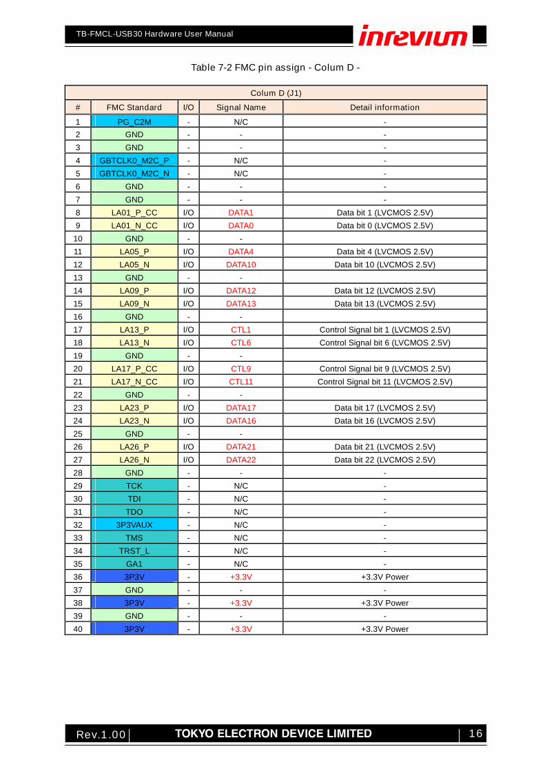
Table 7-2 FMC pin assign - Colum D -
Colum D (J1)
# FMC Standard I/O Signal Name Detail information
1 PG_C2M - N/C - 2 GND - - - 3 GND - - - 4 GBTCLK0_M2C_P - N/C - 5 GBTCLK0_M2C_N - N/C - 6 GND - - - 7 GND - - - 8 LA01_P_CC I/O DATA1 Data bit 1 (LVCMOS 2.5V) 9 LA01_N_CC I/O DATA0 Data bit 0 (LVCMOS 2.5V)
10 GND - - 11 LA05_P I/O DATA4 Data bit 4 (LVCMOS 2.5V) 12 LA05_N I/O DATA10 Data bit 10 (LVCMOS 2.5V) 13 GND - - 14 LA09_P I/O DATA12 Data bit 12 (LVCMOS 2.5V) 15 LA09_N I/O DATA13 Data bit 13 (LVCMOS 2.5V) 16 GND - - 17 LA13_P I/O CTL1 Control Signal bit 1 (LVCMOS 2.5V) 18 LA13_N I/O CTL6 Control Signal bit 6 (LVCMOS 2.5V) 19 GND - - 20 LA17_P_CC I/O CTL9 Control Signal bit 9 (LVCMOS 2.5V) 21 LA17_N_CC I/O CTL11 Control Signal bit 11 (LVCMOS 2.5V) 22 GND - - 23 LA23_P I/O DATA17 Data bit 17 (LVCMOS 2.5V) 24 LA23_N I/O DATA16 Data bit 16 (LVCMOS 2.5V) 25 GND - - 26 LA26_P I/O DATA21 Data bit 21 (LVCMOS 2.5V) 27 LA26_N I/O DATA22 Data bit 22 (LVCMOS 2.5V) 28 GND - - - 29 TCK - N/C - 30 TDI - N/C - 31 TDO - N/C - 32 3P3VAUX - N/C - 33 TMS - N/C - 34 TRST_L - N/C - 35 GA1 - N/C - 36 3P3V - +3.3V +3.3V Power 37 GND - - - 38 3P3V - +3.3V +3.3V Power 39 GND - - - 40 3P3V - +3.3V +3.3V Power
TB-FMCL-USB30 Hardware User Manual
17 Rev.1.00
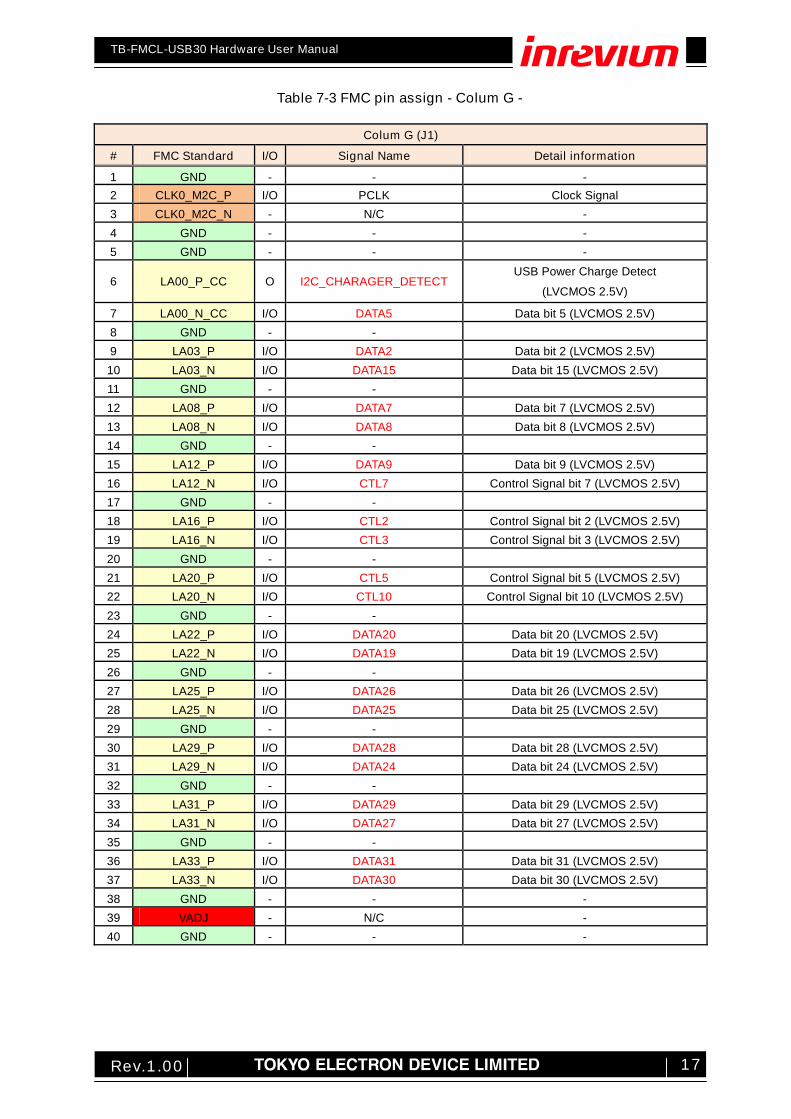
Table 7-3 FMC pin assign - Colum G -
Colum G (J1)
# FMC Standard I/O Signal Name Detail information
1 GND - - - 2 CLK0_M2C_P I/O PCLK Clock Signal 3 CLK0_M2C_N - N/C - 4 GND - - - 5 GND - - -
6 LA00_P_CC O I2C_CHARAGER_DETECT USB Power Charge Detect
(LVCMOS 2.5V)
7 LA00_N_CC I/O DATA5 Data bit 5 (LVCMOS 2.5V) 8 GND - - 9 LA03_P I/O DATA2 Data bit 2 (LVCMOS 2.5V) 10 LA03_N I/O DATA15 Data bit 15 (LVCMOS 2.5V) 11 GND - - 12 LA08_P I/O DATA7 Data bit 7 (LVCMOS 2.5V) 13 LA08_N I/O DATA8 Data bit 8 (LVCMOS 2.5V) 14 GND - - 15 LA12_P I/O DATA9 Data bit 9 (LVCMOS 2.5V) 16 LA12_N I/O CTL7 Control Signal bit 7 (LVCMOS 2.5V) 17 GND - - 18 LA16_P I/O CTL2 Control Signal bit 2 (LVCMOS 2.5V) 19 LA16_N I/O CTL3 Control Signal bit 3 (LVCMOS 2.5V) 20 GND - - 21 LA20_P I/O CTL5 Control Signal bit 5 (LVCMOS 2.5V) 22 LA20_N I/O CTL10 Control Signal bit 10 (LVCMOS 2.5V) 23 GND - - 24 LA22_P I/O DATA20 Data bit 20 (LVCMOS 2.5V) 25 LA22_N I/O DATA19 Data bit 19 (LVCMOS 2.5V) 26 GND - - 27 LA25_P I/O DATA26 Data bit 26 (LVCMOS 2.5V) 28 LA25_N I/O DATA25 Data bit 25 (LVCMOS 2.5V) 29 GND - - 30 LA29_P I/O DATA28 Data bit 28 (LVCMOS 2.5V) 31 LA29_N I/O DATA24 Data bit 24 (LVCMOS 2.5V) 32 GND - - 33 LA31_P I/O DATA29 Data bit 29 (LVCMOS 2.5V) 34 LA31_N I/O DATA27 Data bit 27 (LVCMOS 2.5V) 35 GND - - 36 LA33_P I/O DATA31 Data bit 31 (LVCMOS 2.5V) 37 LA33_N I/O DATA30 Data bit 30 (LVCMOS 2.5V) 38 GND - - - 39 VADJ - N/C - 40 GND - - -
TB-FMCL-USB30 Hardware User Manual
18 Rev.1.00
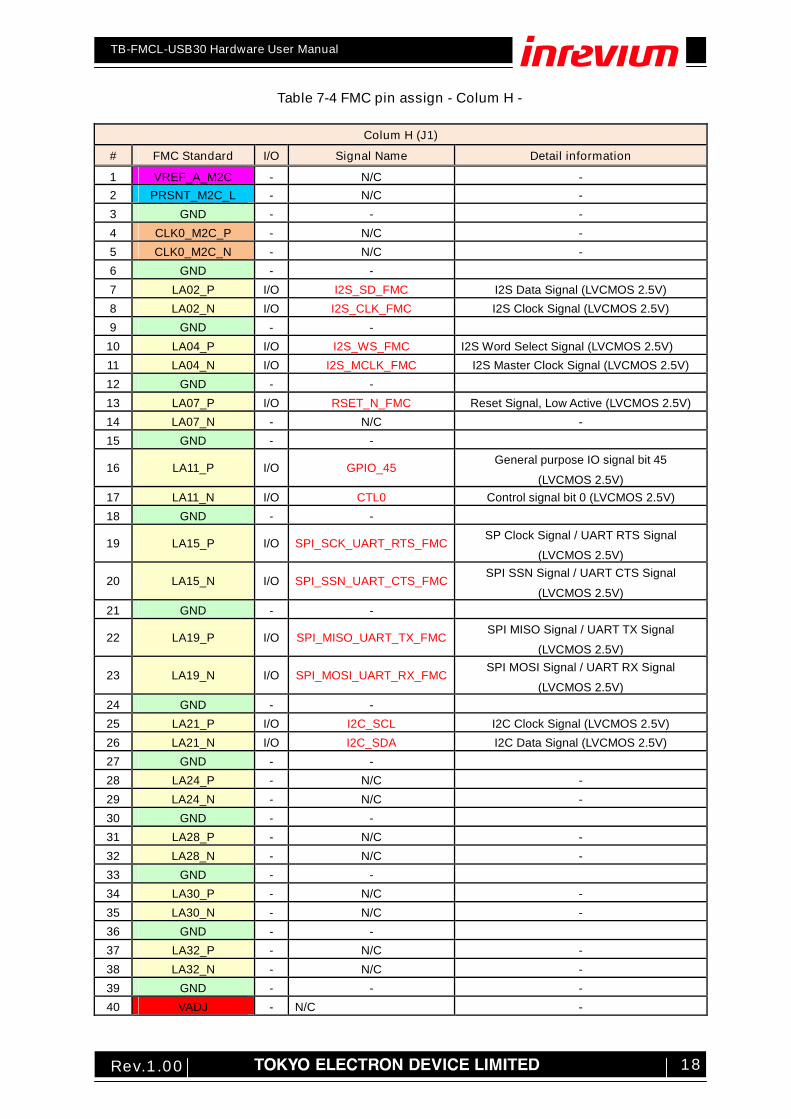
Table 7-4 FMC pin assign - Colum H -
Colum H (J1)
# FMC Standard I/O Signal Name Detail information
1 VREF_A_M2C - N/C - 2 PRSNT_M2C_L - N/C - 3 GND - - - 4 CLK0_M2C_P - N/C - 5 CLK0_M2C_N - N/C - 6 GND - - 7 LA02_P I/O I2S_SD_FMC I2S Data Signal (LVCMOS 2.5V) 8 LA02_N I/O I2S_CLK_FMC I2S Clock Signal (LVCMOS 2.5V) 9 GND - -
10 LA04_P I/O I2S_WS_FMC I2S Word Select Signal (LVCMOS 2.5V) 11 LA04_N I/O I2S_MCLK_FMC I2S Master Clock Signal (LVCMOS 2.5V) 12 GND - - 13 LA07_P I/O RSET_N_FMC Reset Signal, Low Active (LVCMOS 2.5V) 14 LA07_N - N/C - 15 GND - -
16 LA11_P I/O GPIO_45 General purpose IO signal bit 45
(LVCMOS 2.5V) 17 LA11_N I/O CTL0 Control signal bit 0 (LVCMOS 2.5V) 18 GND - -
19 LA15_P I/O SPI_SCK_UART_RTS_FMC SP Clock Signal / UART RTS Signal
(LVCMOS 2.5V)
20 LA15_N I/O SPI_SSN_UART_CTS_FMC SPI SSN Signal / UART CTS Signal
(LVCMOS 2.5V) 21 GND - -
22 LA19_P I/O SPI_MISO_UART_TX_FMC SPI MISO Signal / UART TX Signal
(LVCMOS 2.5V)
23 LA19_N I/O SPI_MOSI_UART_RX_FMC SPI MOSI Signal / UART RX Signal
(LVCMOS 2.5V) 24 GND - - 25 LA21_P I/O I2C_SCL I2C Clock Signal (LVCMOS 2.5V) 26 LA21_N I/O I2C_SDA I2C Data Signal (LVCMOS 2.5V) 27 GND - - 28 LA24_P - N/C - 29 LA24_N - N/C - 30 GND - - 31 LA28_P - N/C - 32 LA28_N - N/C - 33 GND - - 34 LA30_P - N/C - 35 LA30_N - N/C - 36 GND - - 37 LA32_P - N/C - 38 LA32_N - N/C - 39 GND - - - 40 VADJ - N/C -
TB-FMCL-USB30 Hardware User Manual
19 Rev.1.00
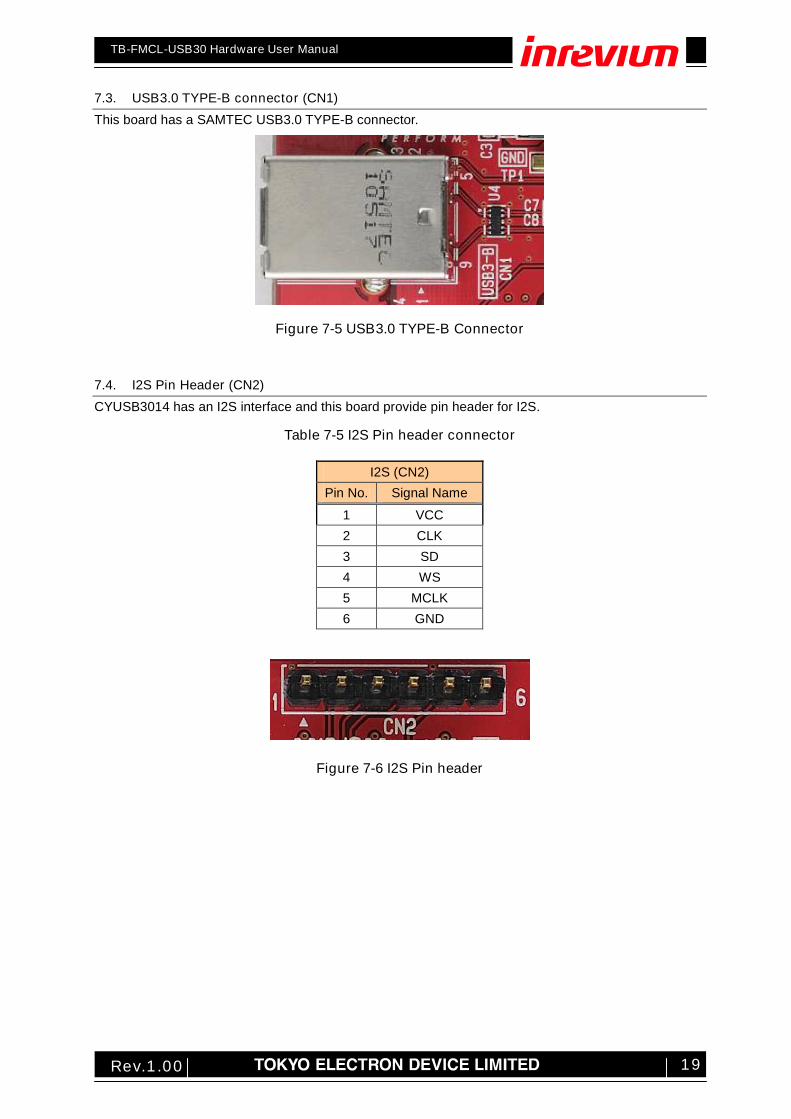
7.3. USB3.0 TYPE-B connector (CN1) This board has a SAMTEC USB3.0 TYPE-B connector.
Figure 7-5 USB3.0 TYPE-B Connector
7.4. I2S Pin Header (CN2) CYUSB3014 has an I2S interface and this board provide pin header for I2S.
Table 7-5 I2S Pin header connector
I2S (CN2) Pin No. Signal Name
1 VCC 2 CLK 3 SD 4 WS 5 MCLK 6 GND
Figure 7-6 I2S Pin header
TB-FMCL-USB30 Hardware User Manual
20 Rev.1.00
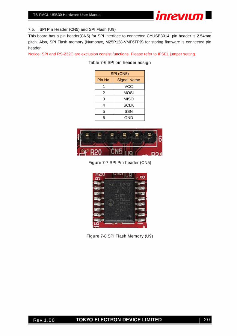
7.5. SPI Pin Header (CN5) and SPI Flash (U9) This board has a pin header(CN5) for SPI interface to connected CYUSB3014. pin header is 2.54mm pitch. Also, SPI Flash memory (Numonyx, M25P128-VMF6TPB) for storing firmware is connected pin header. Notice: SPI and RS-232C are exclusion consist functions. Please refer to IFSEL jumper setting.
Table 7-6 SPI pin header assign
SPI (CN5) Pin No. Signal Name
1 VCC 2 MOSI 3 MISO 4 SCLK 5 SSN 6 GND
Figure 7-7 SPI Pin header (CN5)
Figure 7-8 SPI Flash Memory (U9)
TB-FMCL-USB30 Hardware User Manual
21 Rev.1.00
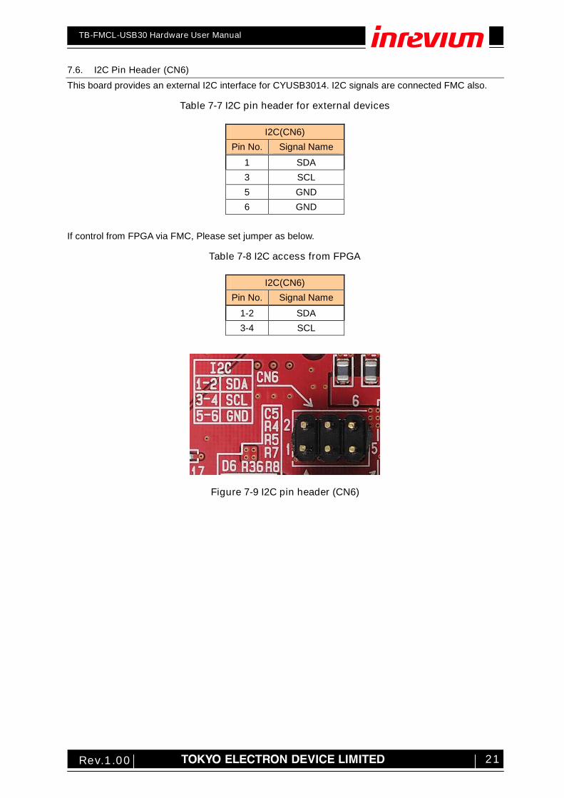
7.6. I2C Pin Header (CN6) This board provides an external I2C interface for CYUSB3014. I2C signals are connected FMC also.
Table 7-7 I2C pin header for external devices
I2C(CN6) Pin No. Signal Name
1 SDA 3 SCL 5 GND 6 GND
If control from FPGA via FMC, Please set jumper as below.
Table 7-8 I2C access from FPGA
I2C(CN6) Pin No. Signal Name
1-2 SDA 3-4 SCL
Figure 7-9 I2C pin header (CN6)
TB-FMCL-USB30 Hardware User Manual
22 Rev.1.00
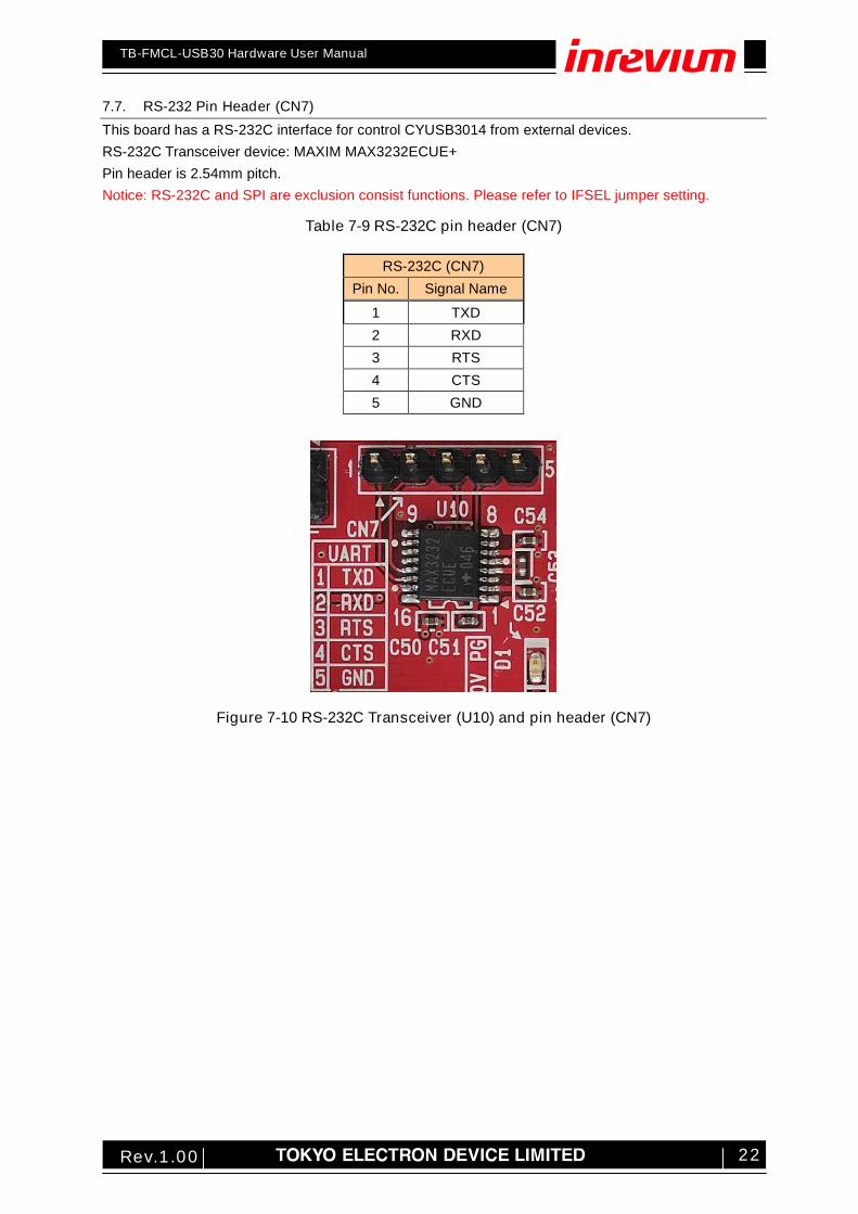
7.7. RS-232 Pin Header (CN7) This board has a RS-232C interface for control CYUSB3014 from external devices. RS-232C Transceiver device: MAXIM MAX3232ECUE+ Pin header is 2.54mm pitch. Notice: RS-232C and SPI are exclusion consist functions. Please refer to IFSEL jumper setting.
Table 7-9 RS-232C pin header (CN7)
RS-232C (CN7) Pin No. Signal Name
1 TXD 2 RXD 3 RTS 4 CTS 5 GND
Figure 7-10 RS-232C Transceiver (U10) and pin header (CN7)
TB-FMCL-USB30 Hardware User Manual
23 Rev.1.00
7.8. LEDs and Push Switch 7.8.1. LED(D1, D3, D4 and D6) 4 LDEs are status of power supply voltage.
Table 7-10 LED Status
LED SILK Description
D1 5V Power Good D3 3.3V Power Good D4 2.5V Power Good D6 1.2V Power Good
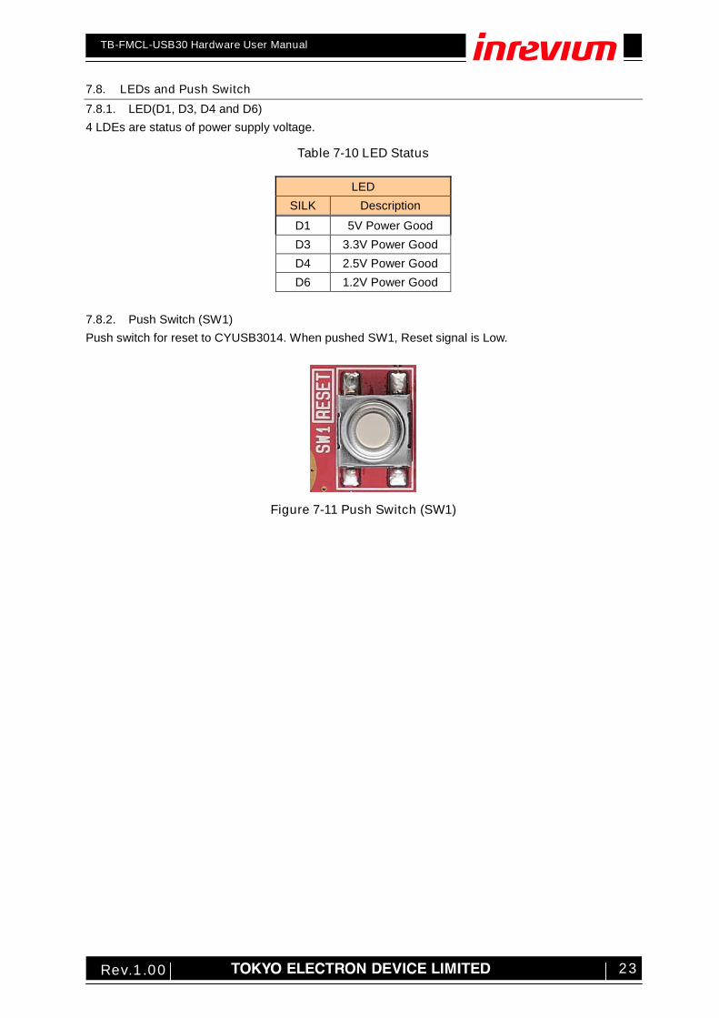
7.8.2. Push Switch (SW1) Push switch for reset to CYUSB3014. When pushed SW1, Reset signal is Low.
Figure 7-11 Push Switch (SW1)
TB-FMCL-USB30 Hardware User Manual
24 Rev.1.00
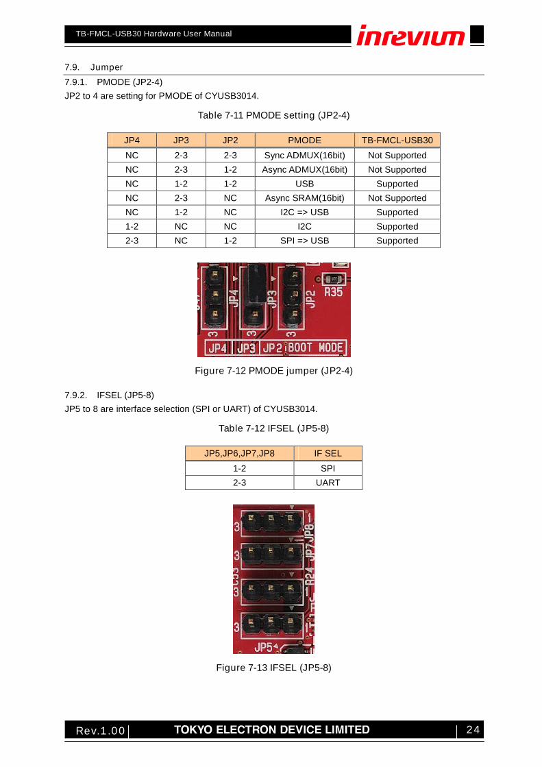
7.9. Jumper 7.9.1. PMODE (JP2-4) JP2 to 4 are setting for PMODE of CYUSB3014.
Table 7-11 PMODE setting (JP2-4)
JP4 JP3 JP2 PMODE TB-FMCL-USB30
NC 2-3 2-3 Sync ADMUX(16bit) Not Supported NC 2-3 1-2 Async ADMUX(16bit) Not Supported NC 1-2 1-2 USB Supported NC 2-3 NC Async SRAM(16bit) Not Supported NC 1-2 NC I2C => USB Supported 1-2 NC NC I2C Supported 2-3 NC 1-2 SPI => USB Supported
Figure 7-12 PMODE jumper (JP2-4)
7.9.2. IFSEL (JP5-8) JP5 to 8 are interface selection (SPI or UART) of CYUSB3014.
Table 7-12 IFSEL (JP5-8)
JP5,JP6,JP7,JP8 IF SEL
1-2 SPI 2-3 UART
Figure 7-13 IFSEL (JP5-8)
TB-FMCL-USB30 Hardware User Manual
25 Rev.1.00
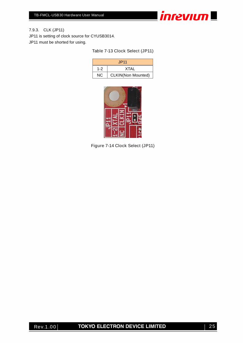
7.9.3. CLK (JP11) JP11 is setting of clock source for CYUSB3014. JP11 must be shorted for using.
Table 7-13 Clock Select (JP11)
JP11
1-2 XTAL NC CLKIN(Non Mounted)
Figure 7-14 Clock Select (JP11)
TB-FMCL-USB30 Hardware User Manual
26 Rev.1.00
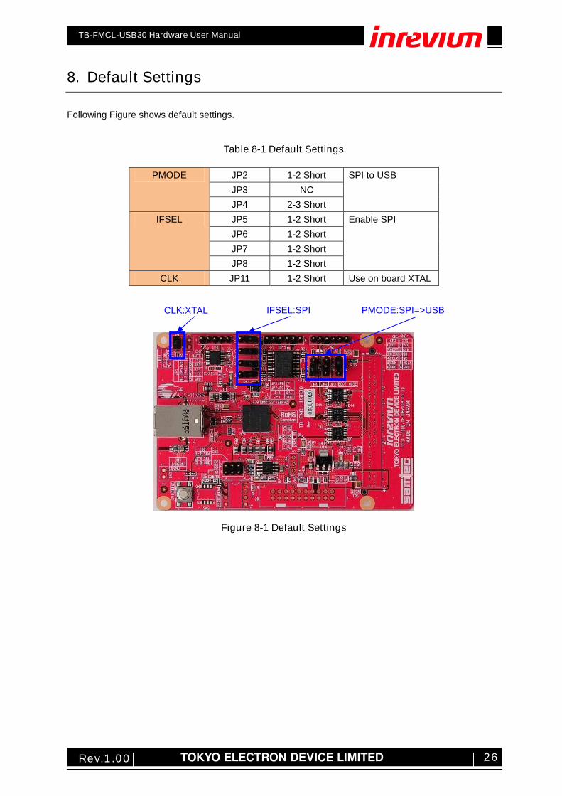
8. Default Settings Following Figure shows default settings.
Table 8-1 Default Settings
PMODE JP2 1-2 Short SPI to USB JP3 NC JP4 2-3 Short
IFSEL JP5 1-2 Short Enable SPI JP6 1-2 Short JP7 1-2 Short JP8 1-2 Short
CLK JP11 1-2 Short Use on board XTAL
Figure 8-1 Default Settings
CLK:XTAL IFSEL:SPI PMODE:SPI=>USB
TB-FMCL-USB30 Hardware User Manual
27 Rev.1.00
PLD Solution Dept. PLD Division URL: http://solutions.inrevium.com/ E-mail: [email protected] HEAD Quarter: Yokohama East Square, 1-4 Kinko-cho, Kanagawa-ku, Yokohama City,
Kanagawa, Japan 221-0056 TEL: +81-45-443-4016 FAX: +81-45-443-4058