Embed Size (px)
Citation preview
翻译日: 2015-11-11
原本: “TB6612FNG” 2014-10-01
本资料是为了参考的目的由原始文档翻译而来。
使用本资料时,请务必确认原始文档关联的最新
信息,并遵守其相关指示。
译文
TB6612FNG

TB6612FNG
2014-10-01 1
译文 TOSHIBA Bi-CD 单晶硅集成电路
TB6612FNG 双 DC 马达驱动 IC
TB6612FNG 是一种驱动 IC,用于带低导通电阻器的 LD MOS 结构
中带输出晶体管的 DC 马达。可利用 IN1 和 IN2 这两个输入信号,选
择 CW,CCW,短路制动器、和停机等四种模式的其中一种模式。
特征
• 电源电压 VM = 15 V(最大值)
• 输出电流 IOUT = 1.2 A(平均值)/3.2 A (峰值)
• 输出低导通电阻器:0.5 Ω (高+低典型值@ VM ≥ 5 V)
• 待机 (省电模式)系统
• CW/CCW/短路制动器/停机功能模式
• 内置热关机电路和低电压检测电路
• 小面封装(SSOP24:0.65 mm 引线间距)
* 本产品带有 MOS 结构,并对静电放电敏感。在处理本产品时,应确保现场环境已配备一根接地母线,一块导电垫和一
个离子产生器进行静电放电保护。确保环境温度和相对湿度维持在合理的水平。
重量: 0.14 g(典型值)
©2014 Toshiba Corporation
TB6612FNG
2014-10-01 2
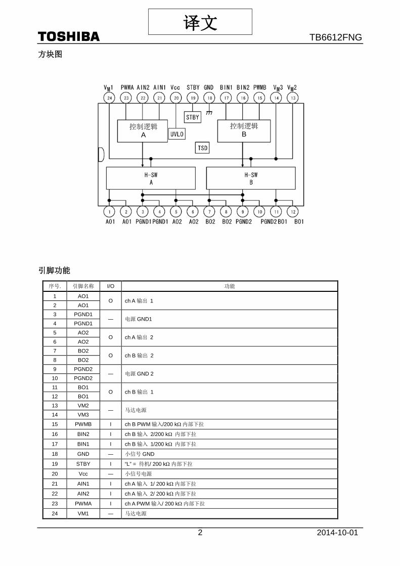
译文 方块图
引脚功能
序号. 引脚名称 I/O 功能
1 AO1 O ch A 输出 1
2 AO1
3 PGND1 ― 电源 GND1
4 PGND1
5 AO2 O ch A 输出 2
6 AO2
7 BO2 O ch B 输出 2
8 BO2
9 PGND2 ― 电源 GND 2
10 PGND2
11 BO1 O ch B 输出 1
12 BO1
13 VM2 ― 马达电源
14 VM3
15 PWMB I ch B PWM 输入/200 kΩ内部下拉
16 BIN2 I ch B 输入 2/200 kΩ 内部下拉
17 BIN1 I ch B 输入 1/200 kΩ 内部下拉
18 GND ― 小信号 GND
19 STBY I “L” = 待机/ 200 kΩ内部下拉
20 Vcc ― 小信号电源
21 AIN1 I ch A 输入 1/ 200 kΩ内部下拉
22 AIN2 I ch A 输入 2/ 200 kΩ内部下拉
23 PWMA I ch A PWM 输入/ 200 kΩ内部下拉
24 VM1 ― 马达电源
控制逻辑 A
控制逻辑 B

TB6612FNG
2014-10-01 3
译文 绝对最大额定值(Ta = 25°C)
工作范围(Ta = -20 ~ 85°C)
特性 符号 额定值 单位 备注
电源电压 VM 15
V
VCC 6
输入电压 VIN -0.2 ~ 6 V IN1,IN2,STBY,PWM 引脚
输出电压 VOUT 15 V O1,O2 引脚
输出电流
IOUT 1.2
A
每 1 ch
IOUT(峰值) 2 tw = 20 ms 连续脉冲, 占空比 ≤ 20%
3.2 tw = 10 ms 单脉冲
功耗 PD
0.78
W
仅 IC
0.89 PCB 贴装时,50 mm × 50 mm t = 1.6 mm Cu ≥ 40%
1.36 PCB 贴装时,76.2 mm × 114.3 mm t = 1.6 mm Cu ≥ 30%
工作温度 Topr -20 ~ 85 °C
贮存温度 Tstg -55 ~ 150 °C
特性 符号 最小值 典型值 最大值 单位 备注
电源电压 VCC 2.7 3 5.5 V
VM 2.5 5 13.5 V
输出电流 (H-SW) IOUT
― ― 1.0
A
VM ≥ 4.5 V
― ― 0.4 4.5 V > VM ≥ 2.5 V
无 PWM 运行
开关频率 fPWM ― ― 100 kHz
输入引脚: 输出引脚:
输入
内部电路
TB6612FNG
2014-10-01 4
译文
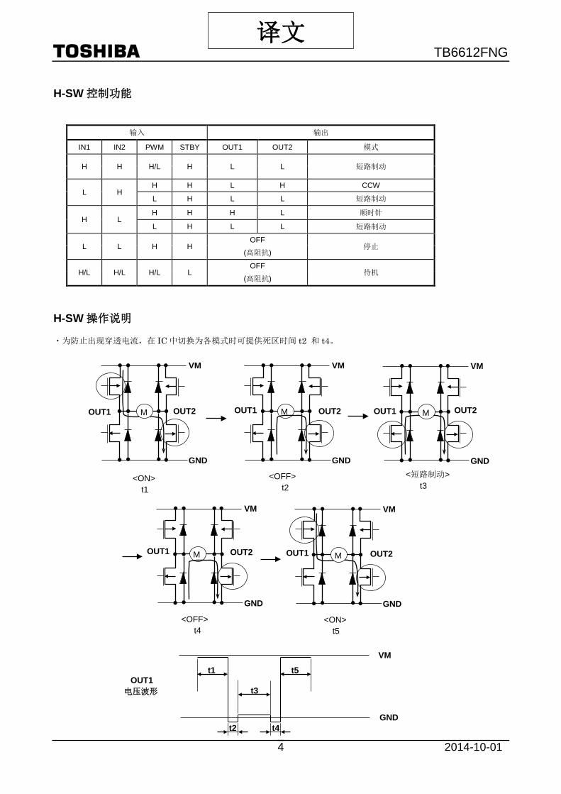
H-SW 控制功能
输入 输出
IN1 IN2 PWM STBY OUT1 OUT2 模式
H H H/L H L L 短路制动
L H H H L H CCW
L H L L 短路制动
H L H H H L 顺时针
L H L L 短路制动
L L H H OFF
(高阻抗) 停止
H/L H/L H/L L OFF
(高阻抗) 待机
H-SW 操作说明
・为防止出现穿透电流,在 IC 中切换为各模式时可提供死区时间 t2 和 t4。
<短路制动> t3
GND
VM
OUT1 电压波形
t1
t2
t3
t5
t4
VM VM VM
M
VM
GND
<ON> t5
M
VM
GND
<OFF> t4
M
GND
M
GND
M
GND
<OFF> t2
<ON> t1
OUT2 OUT1 OUT1 OUT1
OUT1 OUT1
OUT2 OUT2
OUT2 OUT2
TB6612FNG
2014-10-01 5
译文 电气特性 (除非另有规定,则 Ta = 25°C, Vcc = 3 V, VM = 5 V)
特性 符号 测试条件 最小值 典型值 最大值 单位
电源电流
ICC(3 V) STBY = Vcc = 3 V, VM = 5 V ― 1.1 1.8 mA
ICC(5.5 V) STBY = Vcc = 5.5 V, VM = 5 V ― 1.5 2.2
ICC(STB) STBY = 0 V
― ― 1 μA
IM(STB) ― ― 1
控制输入电压 VIH
― Vcc×0.7 ― Vcc+0.2
V VIL -0.2 ― Vcc×0.3
控制输入电流 IIH VIN = 3 V 5 15 25
μA IIL VIN = 0 V ― ― 1
待机输入电压 VIH(STB)
― Vcc×0.7 ― Vcc+0.2
V VIL(STB) -0.2 ― Vcc×0.3
待机输入电流 IIH(STB) VIN = 3 V 5 15 25
μA IIL(STB) VIN = 0 V ― ― 1
输出饱和电压 Vsat(U+L)1 IO = 1 A, Vcc = VM = 5 V ― 0.5 0.7
V Vsat(U+L)2 IO= 0.3 A, Vcc = VM = 5 V ― 0.15 0.21
输出泄漏电流 IL(U) VM = VOUT = 15 V ― ― 1
μA IL(L) VM = 15 V, VOUT = 0 V -1 ― ―
再生二极管 VF VF(U)
IF = 1A ― 1 1.1
V VF(L) ― 1 1.1
低电压检测
电压 UVLD
(仅为设计目标) ― 1.9 ―
V
恢复电压 UVLC ― 2.2 ―
响应速度
tr (仅为设计目标)
― 24 ―
ns tf ― 41 ―
死区
时间
H ~ L 穿透保护时间
(仅为设计目标)
― 50 ―
L ~ H ― 230 ―
过热关机电路
工作温度 TSD
(仅为设计目标)
― 175 ―
°C 热击穿
迟滞 ∆TSD ― 20 ―

TB6612FNG
2014-10-01 6
译文 目标特性
PD - Ta
0.00
0.50
1.00
1.50
0 50 100 150Ta (℃)
(w)
①
②
①IC単体θj-a=160℃/W②基板実装時
PCB面積 50×50×1.6mm
Cu箔面積≧40%
③基板実装時
PCB面積 76.2×114.3×1.6mm
Cu箔面積≧30%
③ ①IC 仅 θj – a = 160°C/W ② 在板上 PCB 面积为 50 mm×50 mm×1.6 mm Cu 面积 ≥ 40% ③ 在板上 PCB 面积为 76.2 mm×114.3 mm×1.6 mm Cu 面积≥ 30%
功耗
PD
PD - Ta
1 ch driving
2 ch driving
Iout - Duty
0.0
0.5
1.0
1.5
2.0
2.5
0% 20% 40% 60% 80% 100%Duty
(A)
2ch動作時
1ch動作時
Ta=25℃,IC単体
输出电流
I OU
T
IOUT -占空比
双通道操作
单通道操作
Ta = 25°C,仅 IC
占空比
TB6612FNG
2014-10-01 7
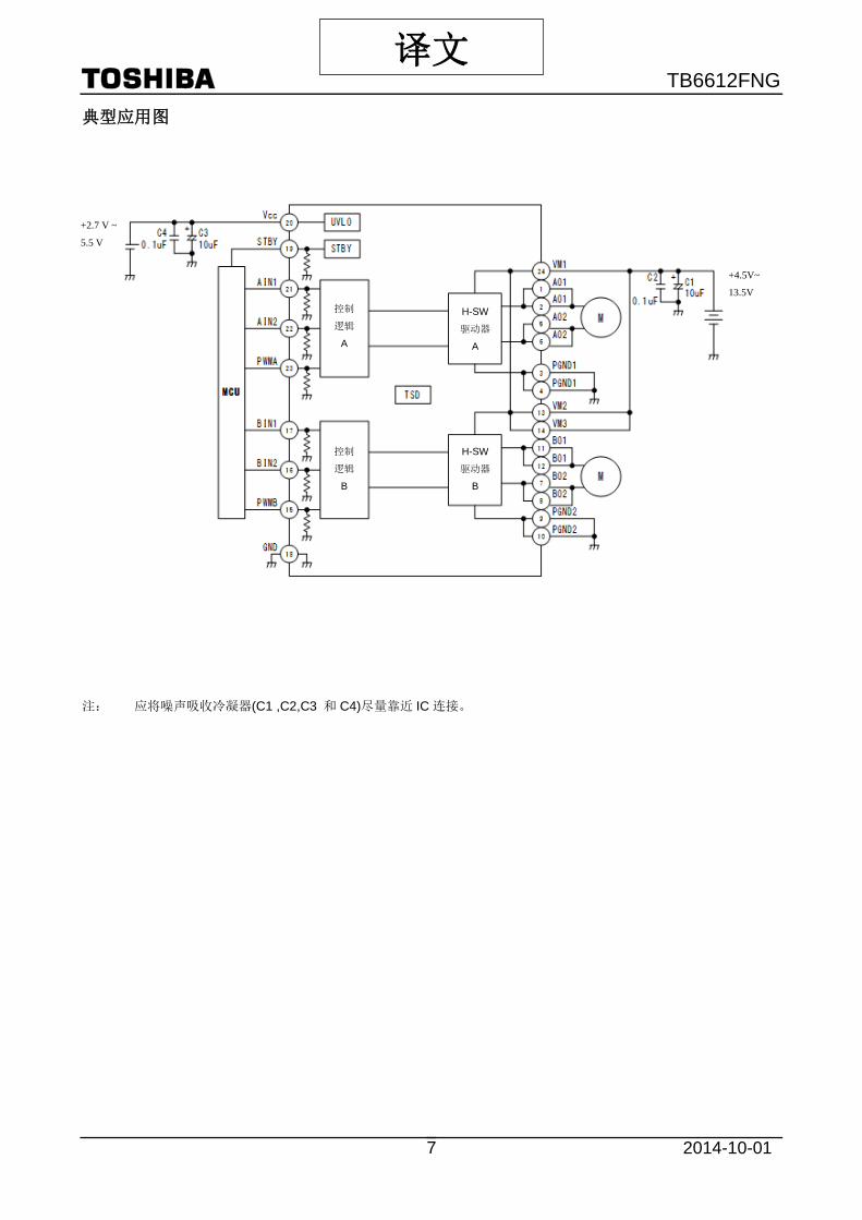
译文 典型应用图
注: 应将噪声吸收冷凝器(C1 ,C2,C3 和 C4)尽量靠近 IC 连接。
控制
逻辑
A
H-SW
驱动器
A
控制
逻辑
B
H-SW
驱动器
B
+2.7 V ~
5.5 V
+4.5V~
13.5V
TB6612FNG
2014-10-01 8
译文
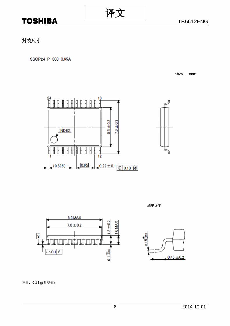
封装尺寸
重量:0.14 g(典型值)
端子详图
“单位: mm”
TB6612FNG
2014-10-01 9
译文 内容注释
1. 方块图 出于解释目的,可能忽略或简化部分功能块,电路或常数。
2. 等效电路 出于解释目的,可能简化等效电路图或忽略其中的一部分。
3. 时序图 出于解释目的,可能简化时序图。
4. 应用电路 本文件所示应用电路仅供参考。在大规范生产设计阶段,必须进行全面评估。
东芝不因提供这些应用电路示例而授予任何工业产权许可。
5. 测试回路 测试回路中的部件仅用于获取及确认装置特性。不保证这些部件和电路能防止在应用设备中发生故障或失效。
IC 使用注意事项 IC 处理注意事项
[1] 半导体装置绝对最大额定值是一套在任何时候都不得超过的额定值。严禁超过这些额定值。
如超过额定值,则可能导致装置故障,损坏或劣化,并可因爆炸或燃烧导致人身伤害。
[2] 为确保在过电流和/或 IC 故障时不会持续通过大电流,应使用适当的电源保险丝。当在超过绝对最大额定
值的条件下使用,接线路径不对,或者在接线或负载处产生异常脉冲噪声而造成大电流持续通过时,IC 会被
完全击穿,并导致烟雾或起火。为尽量减小击穿时大电流流过的影响,必须进行正确设置,例如保险丝容
量,熔断时间及插入电路的位置。
[3] 如您的设计包括诸如电机线圈之类的电感负荷,应将保护电路结合到设计中,以防止设备发生故障,或被
接通电源时涌流导致的电流或断电时反电动势产生的负电流所击穿。进而造成伤害,烟雾或起火。
应使用带 IC 的具有内置保护功能的稳定电源。若电源不稳定,保护功能可能不工作而造成集成电路击穿,
进而造成伤害,烟雾或起火。
[4] 严禁装置插错方向或插入错误。
保证电源的正负极端子接线正确。
否则电流消耗或功耗会超过绝对最大额定值而造成装置击穿,损坏或变坏,并因爆炸或燃烧而使人受伤。
此外,严禁任何阻止插错方向或插入错误,哪怕对其施加电流只有一次。

TB6612FNG
2014-10-01 10
译文
IC 处理记住要点
(1) 热关机电路
热关机电路不一定能在所有情况下对 IC 进行保护。若热关机电路在超温下工作,应立即消除发热状况。
视使用方法及使用条件而定,超过绝对最大额定值会造成热关机电路不能正常工作或者造成 IC 在工作前击
穿。
(2) 热辐射设计
在使用功率放大器、稳压器或驱动器等电流较大的 IC 时,该装置的设计应能确保适当散热,并在任何时间
和情况下均不会超过所规定的结温(Tj)。这些 IC 甚至在正常使用时会发热。对于 IC 散热不足的设计,会造
成 IC 特性变差或击穿。此外,在设计装置时,请考虑集成电路散热对外围部件的影响。
(3) 反电动势
当电机突然反转,停止或放慢时,由于反电动势的影响,电流会回流到电机电源。若电源的电流吸收能力
小,装置的电机电源和输出引脚就会存在超过绝对最大额定值的风险。为了避免出现这种问题,在系统设
计中应考虑反电动势的影响。
TB6612FNG
2014-10-01 11
译文 RESTRICTIONS ON PRODUCT USE
• Toshiba Corporation, and its subsidiaries and affiliates (collectively "TOSHIBA"), reserve the right to make changes to the information in this document, and related hardware, software and systems (collectively "Product") without notice.
• This document and any information herein may not be reproduced without prior written permission from TOSHIBA. Even with TOSHIBA's written permission, reproduction is permissible only if reproduction is without alteration/omission.
• Though TOSHIBA works continually to improve Product's quality and reliability, Product can malfunction or fail. Customers are responsible for complying with safety standards and for providing adequate designs and safeguards for their hardware, software and systems which minimize risk and avoid situations in which a malfunction or failure of Product could cause loss of human life, bodily injury or damage to property, including data loss or corruption. Before customers use the Product, create designs including the Product, or incorporate the Product into their own applications, customers must also refer to and comply with (a) the latest versions of all relevant TOSHIBA information, including without limitation, this document, the specifications, the data sheets and application notes for Product and the precautions and conditions set forth in the "TOSHIBA Semiconductor Reliability Handbook" and (b) the instructions for the application with which the Product will be used with or for. Customers are solely responsible for all aspects of their own product design or applications, including but not limited to (a) determining the appropriateness of the use of this Product in such design or applications; (b) evaluating and determining the applicability of any information contained in this document, or in charts, diagrams, programs, algorithms, sample application circuits, or any other referenced documents; and (c) validating all operating parameters for such designs and applications. TOSHIBA ASSUMES NO LIABILITY FOR CUSTOMERS' PRODUCT DESIGN OR APPLICATIONS.
• PRODUCT IS NEITHER INTENDED NOR WARRANTED FOR USE IN EQUIPMENTS OR SYSTEMS THAT REQUIRE EXTRAORDINARILY HIGH LEVELS OF QUALITY AND/OR RELIABILITY, AND/OR A MALFUNCTION OR FAILURE OF WHICH MAY CAUSE LOSS OF HUMAN LIFE, BODILY INJURY, SERIOUS PROPERTY DAMAGE AND/OR SERIOUS PUBLIC IMPACT ("UNINTENDED USE"). Except for specific applications as expressly stated in this document, Unintended Use includes, without limitation, equipment used in nuclear facilities, equipment used in the aerospace industry, medical equipment, equipment used for automobiles, trains, ships and other transportation, traffic signaling equipment, equipment used to control combustions or explosions, safety devices, elevators and escalators, devices related to electric power, and equipment used in finance-related fields. IF YOU USE PRODUCT FOR UNINTENDED USE, TOSHIBA ASSUMES NO LIABILITY FOR PRODUCT. For details, please contact your TOSHIBA sales representative.
• Do not disassemble, analyze, reverse-engineer, alter, modify, translate or copy Product, whether in whole or in part.
• Product shall not be used for or incorporated into any products or systems whose manufacture, use, or sale is prohibited under any applicable laws or regulations.
• The information contained herein is presented only as guidance for Product use. No responsibility is assumed by TOSHIBA for any infringement of patents or any other intellectual property rights of third parties that may result from the use of Product. No license to any intellectual property right is granted by this document, whether express or implied, by estoppel or otherwise.
• ABSENT A WRITTEN SIGNED AGREEMENT, EXCEPT AS PROVIDED IN THE RELEVANT TERMS AND CONDITIONS OF SALE FOR PRODUCT, AND TO THE MAXIMUM EXTENT ALLOWABLE BY LAW, TOSHIBA (1) ASSUMES NO LIABILITY WHATSOEVER, INCLUDING WITHOUT LIMITATION, INDIRECT, CONSEQUENTIAL, SPECIAL, OR INCIDENTAL DAMAGES OR LOSS, INCLUDING WITHOUT LIMITATION, LOSS OF PROFITS, LOSS OF OPPORTUNITIES, BUSINESS INTERRUPTION AND LOSS OF DATA, AND (2) DISCLAIMS ANY AND ALL EXPRESS OR IMPLIED WARRANTIES AND CONDITIONS RELATED TO SALE, USE OF PRODUCT, OR INFORMATION, INCLUDING WARRANTIES OR CONDITIONS OF MERCHANTABILITY, FITNESS FOR A PARTICULAR PURPOSE, ACCURACY OF INFORMATION, OR NONINFRINGEMENT.
• Do not use or otherwise make available Product or related software or technology for any military purposes, including without limitation, for the design, development, use, stockpiling or manufacturing of nuclear, chemical, or biological weapons or missile technology products (mass destruction weapons). Product and related software and technology may be controlled under the applicable export laws and regulations including, without limitation, the Japanese Foreign Exchange and Foreign Trade Law and the U.S. Export Administration Regulations. Export and re-export of Product or related software or technology are strictly prohibited except in compliance with all applicable export laws and regulations.
• Please contact your TOSHIBA sales representative for details as to environmental matters such as the RoHS compatibility of Product. Please use Product in compliance with all applicable laws and regulations that regulate the inclusion or use of controlled substances, including without limitation, the EU RoHS Directive. TOSHIBA ASSUMES NO LIABILITY FOR DAMAGES OR LOSSES OCCURRING AS A RESULT OF NONCOMPLIANCE WITH APPLICABLE LAWS AND REGULATIONS.