Embed Size (px)
Citation preview
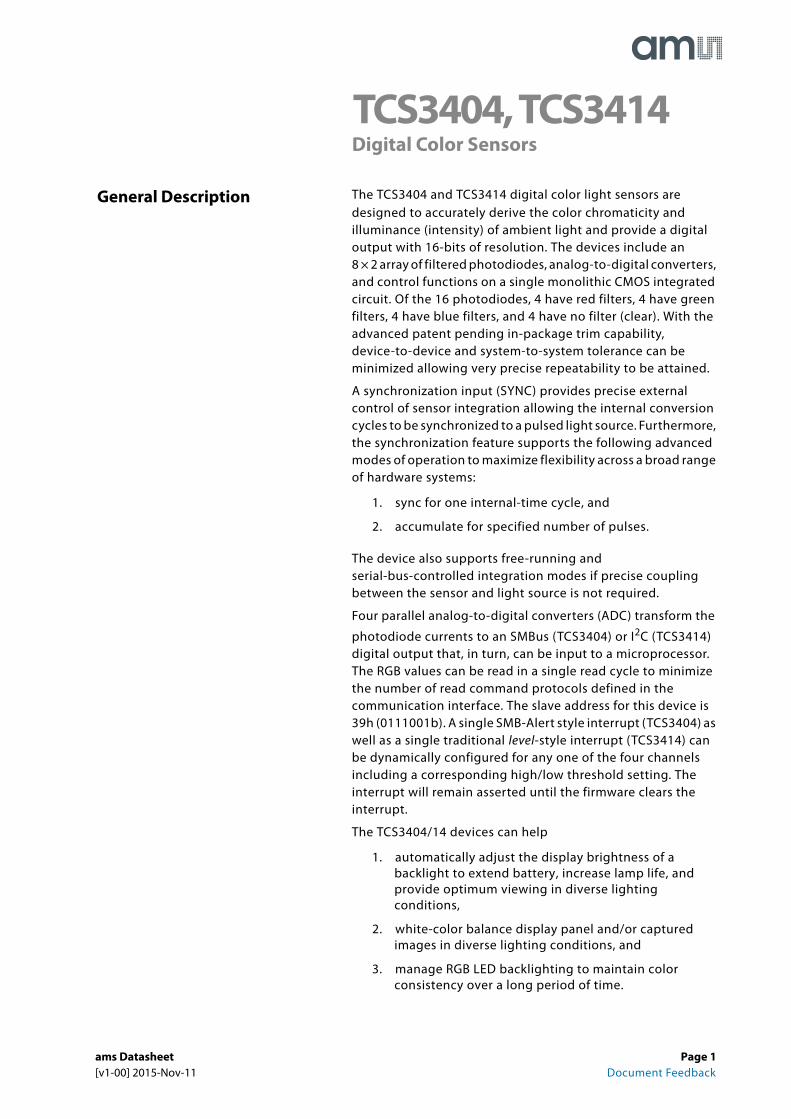
TCS3404, TCS3414Digital Color Sensors
The TCS3404 and TCS3414 digital color light sensors are designed to accurately derive the color chromaticity and illuminance (intensity) of ambient light and provide a digital output with 16-bits of resolution. The devices include an8 × 2 array of filtered photodiodes, analog-to-digital converters, and control functions on a single monolithic CMOS integrated circuit. Of the 16 photodiodes, 4 have red filters, 4 have green filters, 4 have blue filters, and 4 have no filter (clear). With the advanced patent pending in-package trim capability, device-to-device and system-to-system tolerance can be minimized allowing very precise repeatability to be attained.
A synchronization input (SYNC) provides precise external control of sensor integration allowing the internal conversion cycles to be synchronized to a pulsed light source. Furthermore, the synchronization feature supports the following advanced modes of operation to maximize flexibility across a broad range of hardware systems:
1. sync for one internal-time cycle, and
2. accumulate for specified number of pulses.
The device also supports free-running and serial-bus-controlled integration modes if precise coupling between the sensor and light source is not required.
Four parallel analog-to-digital converters (ADC) transform the
photodiode currents to an SMBus (TCS3404) or I2C (TCS3414) digital output that, in turn, can be input to a microprocessor. The RGB values can be read in a single read cycle to minimize the number of read command protocols defined in the communication interface. The slave address for this device is 39h (0111001b). A single SMB-Alert style interrupt (TCS3404) as well as a single traditional level-style interrupt (TCS3414) can be dynamically configured for any one of the four channels including a corresponding high/low threshold setting. The interrupt will remain asserted until the firmware clears the interrupt.
The TCS3404/14 devices can help
1. automatically adjust the display brightness of a backlight to extend battery, increase lamp life, and provide optimum viewing in diverse lighting conditions,
2. white-color balance display panel and/or captured images in diverse lighting conditions, and
3. manage RGB LED backlighting to maintain color consistency over a long period of time.
General Description
ams Datasheet Page 1[v1-00] 2015-Nov-11 Document Feedback
TCS3404, TCS3414 − General Description
These devices are also ideal in controlling keyboard illumination in low ambient light conditions. Chromaticity coordinates (x,y) can be used to derive color temperature for the purpose of white-color balancing of displays and/or captured images. Illuminance, in lux, can be used to approximate the human eye response of ambient light and to manage exposure control in digital cameras. The TCS3404/14 devices are ideal in notebook/tablet PCs, LCD monitors, flat-panel televisions, cell phones, and digital cameras. Additional applications include street light control, security lighting, sunlight harvesting, and automotive instrumentation clusters.
Ordering Information and Content Guide appear at end of datasheet.
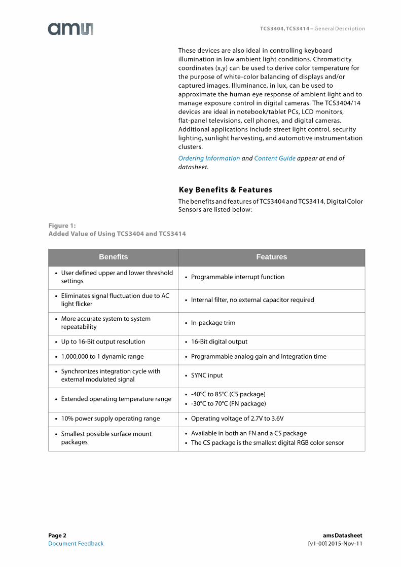
Key Benefits & FeaturesThe benefits and features of TCS3404 and TCS3414, Digital Color Sensors are listed below:
Figure 1:Added Value of Using TCS3404 and TCS3414
Benefits Features
• User defined upper and lower threshold settings
• Programmable interrupt function
• Eliminates signal fluctuation due to AC light flicker
• Internal filter, no external capacitor required
• More accurate system to system repeatability
• In-package trim
• Up to 16-Bit output resolution • 16-Bit digital output
• 1,000,000 to 1 dynamic range • Programmable analog gain and integration time
• Synchronizes integration cycle with external modulated signal
• SYNC input
• Extended operating temperature range• -40°C to 85°C (CS package)• -30°C to 70°C (FN package)
• 10% power supply operating range • Operating voltage of 2.7V to 3.6V
• Smallest possible surface mount packages
• Available in both an FN and a CS package• The CS package is the smallest digital RGB color sensor
Page 2 ams Datasheet Document Feedback [v1-00] 2015-Nov-11
TCS3404, TCS3414 − General Description
ApplicationsThe applications of this device are:
• Provides method to derive chromaticity coordinates to manage display backlighting (i.e. RGB LED, CCFL, etc.)
• Provides means to derive color temperature to white-color balance displays under various lighting conditions
End Products and Market Segments
• HDTVs
• Tablets, laptops, monitors
• Medical instrumentation
• Consumer toys
• Industrial/commercial lighting
• Industrial process control
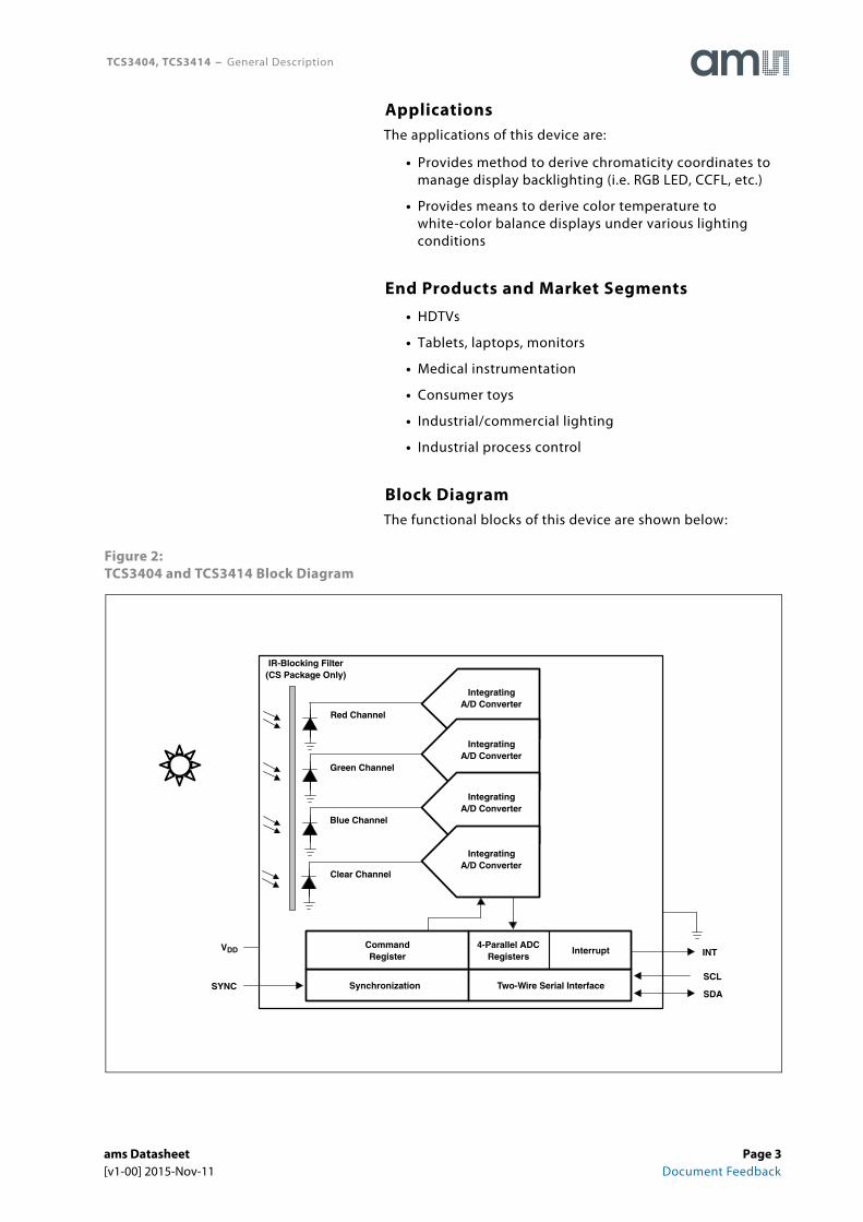
Block DiagramThe functional blocks of this device are shown below:
Figure 2:TCS3404 and TCS3414 Block Diagram
Two-Wire Serial Interface
Interrupt
SDA
VDD
Blue Channel
Clear Channel
CommandRegister
4-Parallel ADCRegisters INT
SCL
Green Channel
Red Channel
IntegratingA/D Converter
IntegratingA/D Converter
IntegratingA/D Converter
IntegratingA/D Converter
SynchronizationSYNC
IR-Blocking Filter(CS Package Only)
ams Datasheet Page 3[v1-00] 2015-Nov-11 Document Feedback
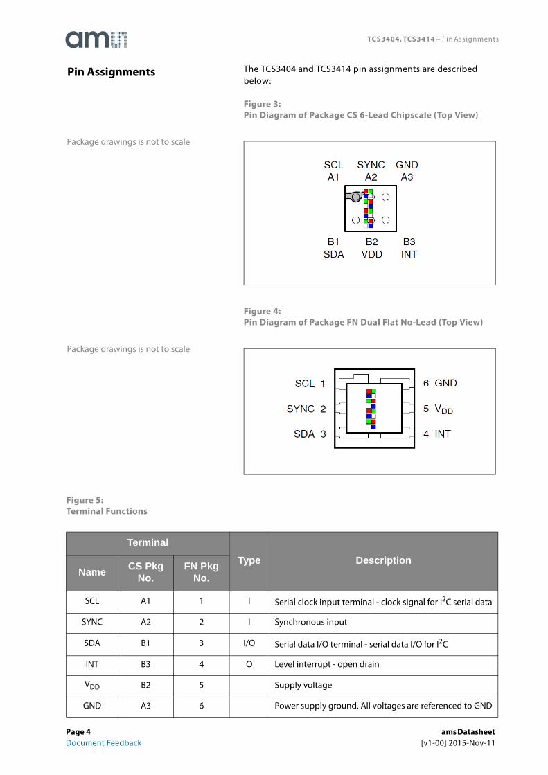
TCS3404, TCS3414 − Pin Assignments
The TCS3404 and TCS3414 pin assignments are described below:
Figure 3:Pin Diagram of Package CS 6-Lead Chipscale (Top View)
Figure 4:Pin Diagram of Package FN Dual Flat No-Lead (Top View)
Figure 5:Terminal Functions
Package drawings is not to scale
Package drawings is not to scale
Terminal
Type DescriptionName
CS Pkg No.
FN Pkg No.
SCL A1 1 I Serial clock input terminal - clock signal for I2C serial data
SYNC A2 2 I Synchronous input
SDA B1 3 I/O Serial data I/O terminal - serial data I/O for I2C
INT B3 4 O Level interrupt - open drain
VDD B2 5 Supply voltage
GND A3 6 Power supply ground. All voltages are referenced to GND
Pin Assignments
Page 4 ams Datasheet Document Feedback [v1-00] 2015-Nov-11

TCS3404, TCS3414 − Absolute Maximum Ratings
Stresses beyond those listed under Absolute Maximum Ratings may cause permanent damage to the device. These are stress ratings only. Functional operation of the device at these or any other conditions beyond those indicated under Recommended Operating Conditions is not implied. Exposure to absolute maximum rating conditions for extended periods may affect device reliability.
Figure 6:Absolute Maximum Ratings over Operating Free-Air Temperature Range (unless otherwise noted)
Note(s):
1. All voltages are with respect to GND.
Symbol Parameter Min Max Unit
VDD Supply voltage (1) 3.8 V
VO Digital output voltage range -0.5 3.8 V
IO Digital output current -1 20 mA
Tstrg Storage temperature range -40 85 °C
ESDHBM ESD tolerance, human body model ±2000 V
Absolute Maximum Ratings
ams Datasheet Page 5[v1-00] 2015-Nov-11 Document Feedback
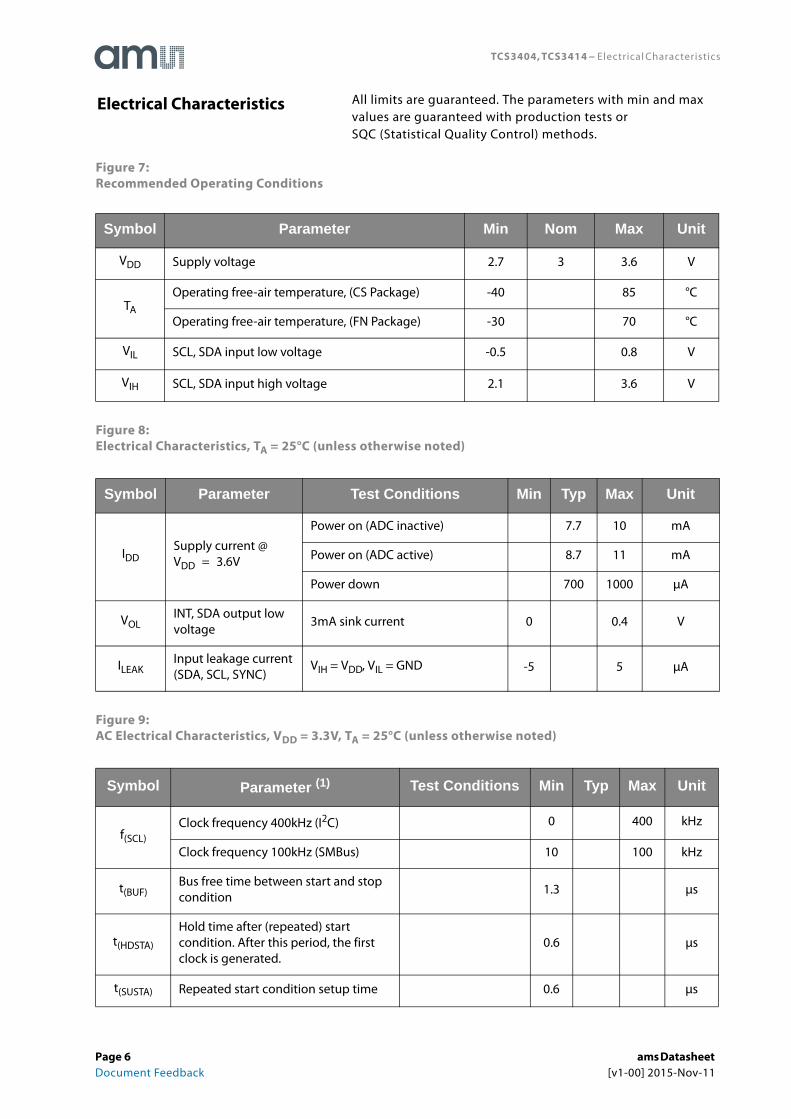
TCS3404, TCS3414 − Electrical Characteristics
All limits are guaranteed. The parameters with min and max values are guaranteed with production tests orSQC (Statistical Quality Control) methods.
Figure 7:Recommended Operating Conditions
Figure 8:Electrical Characteristics, TA = 25°C (unless otherwise noted)
Figure 9:AC Electrical Characteristics, VDD = 3.3V, TA = 25°C (unless otherwise noted)
Symbol Parameter Min Nom Max Unit
VDD Supply voltage 2.7 3 3.6 V
TA
Operating free-air temperature, (CS Package) -40 85 °C
Operating free-air temperature, (FN Package) -30 70 °C
VIL SCL, SDA input low voltage -0.5 0.8 V
VIH SCL, SDA input high voltage 2.1 3.6 V
Symbol Parameter Test Conditions Min Typ Max Unit
IDDSupply current @ VDD = 3.6V
Power on (ADC inactive) 7.7 10 mA
Power on (ADC active) 8.7 11 mA
Power down 700 1000 μA
VOLINT, SDA output low voltage
3mA sink current 0 0.4 V
ILEAKInput leakage current(SDA, SCL, SYNC)
VIH = VDD, VIL = GND -5 5 μA
Symbol Parameter (1) Test Conditions Min Typ Max Unit
f(SCL)Clock frequency 400kHz (I2C) 0 400 kHz
Clock frequency 100kHz (SMBus) 10 100 kHz
t(BUF)Bus free time between start and stop condition
1.3 μs
t(HDSTA)
Hold time after (repeated) start condition. After this period, the first clock is generated.
0.6 μs
t(SUSTA) Repeated start condition setup time 0.6 μs
Electrical Characteristics
Page 6 ams Datasheet Document Feedback [v1-00] 2015-Nov-11
TCS3404, TCS3414 − Electrical Characteristics
Note(s):
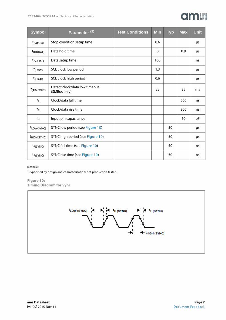
1. Specified by design and characterization; not production tested.
Figure 10:Timing Diagram for Sync
t(SUSTO) Stop condition setup time 0.6 μs
t(HDDAT) Data hold time 0 0.9 μs
t(SUDAT) Data setup time 100 ns
t(LOW) SCL clock low period 1.3 μs
t(HIGH) SCL clock high period 0.6 μs
t(TIMEOUT)Detect clock/data low timeout(SMBus only)
25 35 ms
tF Clock/data fall time 300 ns
tR Clock/data rise time 300 ns
Ci Input pin capacitance 10 pF
tLOW(SYNC) SYNC low period (see Figure 10) 50 μs
tHIGH(SYNC) SYNC high period (see Figure 10) 50 μs
tF(SYNC) SYNC fall time (see Figure 10) 50 ns
tR(SYNC) SYNC rise time (see Figure 10) 50 ns
Symbol Parameter (1) Test Conditions Min Typ Max Unit
ams Datasheet Page 7[v1-00] 2015-Nov-11 Document Feedback
ams Datasheet [v1-00] 2015-Nov-11
T C S 3 4 0 4 , T C S 3 4 1 4 − Electrical Characteristics
70nm, spectral halfwidth Δλ½ = 35nm, and
24nm, spectral halfwidth Δλ½ = 47nm, and
0nm, spectral halfwidth Δλ½ = 17nm, and
s 3, 4, and 5 and using 1lx = 1lm/m2.
annel Clear ChannelUnit
Max Min Typ Max
90% 59.0 65.6 72.5
counts/ (μW/cm2)
35% 71.2 76.9 82.7
15% 80.6 90.1 99.5
90% 56.3 62.5 69.1
counts/ (μW/cm2)
35% 72.5 78.4 84.3
15% 94.2 105.3 116.3
Page 8Document Feedback
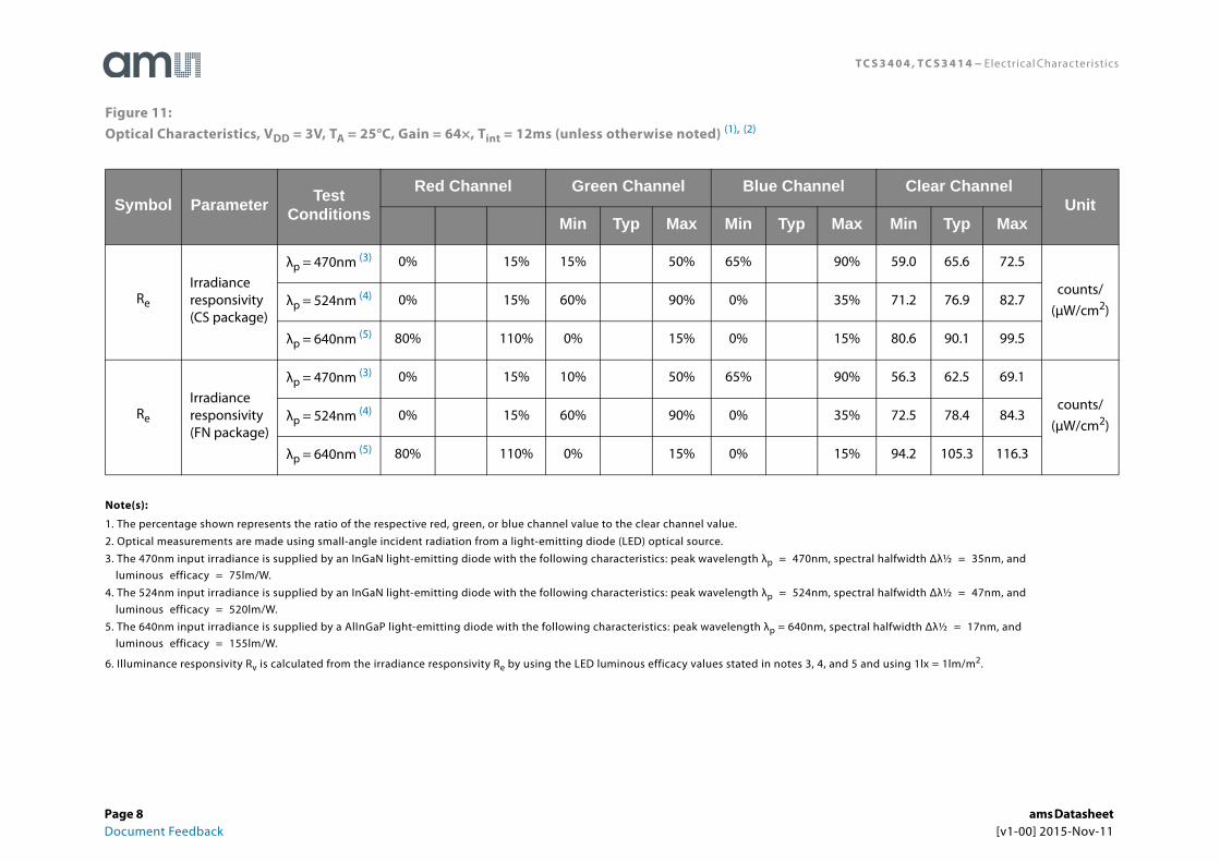
Figure 11:Optical Characteristics, VDD = 3V, TA = 25°C, Gain = 64×, Tint = 12ms (unless otherwise noted) (1), (2)
Note(s):
1. The percentage shown represents the ratio of the respective red, green, or blue channel value to the clear channel value.
2. Optical measurements are made using small-angle incident radiation from a light-emitting diode (LED) optical source.
3. The 470nm input irradiance is supplied by an InGaN light-emitting diode with the following characteristics: peak wavelength λp = 4luminous efficacy = 75lm/W.
4. The 524nm input irradiance is supplied by an InGaN light-emitting diode with the following characteristics: peak wavelength λp = 5luminous efficacy = 520lm/W.
5. The 640nm input irradiance is supplied by a AlInGaP light-emitting diode with the following characteristics: peak wavelength λp = 64luminous efficacy = 155lm/W.
6. Illuminance responsivity Rv is calculated from the irradiance responsivity Re by using the LED luminous efficacy values stated in note
Symbol ParameterTest
Conditions
Red Channel Green Channel Blue Ch
Min Typ Max Min Typ
Re
Irradiance responsivity (CS package)
λp = 470nm (3) 0% 15% 15% 50% 65%
λp = 524nm (4) 0% 15% 60% 90% 0%
λp = 640nm (5) 80% 110% 0% 15% 0%
Re
Irradiance responsivity (FN package)
λp = 470nm (3) 0% 15% 10% 50% 65%
λp = 524nm (4) 0% 15% 60% 90% 0%
λp = 640nm (5) 80% 110% 0% 15% 0%

TCS3404, TCS3414 − Electrical Characteristics
Figure 12:Optical Characteristics, VDD = 3V, TA = 25°C (unless otherwise noted) (2), (3), (4)
Note(s):
1. At shorter integration times and/or higher Prescale settings, the device will reach saturation of the analog section before the digital count reaches the maximum 16-bit value. The worst-case (lowest) analog saturation value can be obtained using the formula: Analog saturation = (fosc(min) ×Tint) ÷ Prescale, where Fosc(min) is the minimum oscillator frequency in Hz, and tint is the actual integration time (internal, manually-timed, or sync-generated) in seconds.
2. Gain is controlled by the gain register (07h) described in the Register section.
3. Measurements taken when the Photodiode field value in the Photodiode Register (06h) is 00b and when the Prescaler field value in the Gain Register (07h) is 000b.
4. The full scale ADC count value is slew-rate limited for short integration times and is limited by the 16-bit counter for long integration times. The nominal transition between the two regions is tint = 65535/5000 = 13.1ms.
Parameter Test Conditions Min Typ Max Unit
Gain scaling, relative to 1× gain setting
4× 3.8 4 4.2
16× 15.2 16 16.8
64× 60.8 64 67.2
Dark ADC count valueEe = 0, 64× gain setting,Tint = 400ms
0 3 15 counts
Maximum digital count value Prescale = 1, Tint = 400ms (1) 65535 counts
fosc Oscillator frequency 4.2 4.4 4.6 MHz
Internal integration time tolerance
-5 5 %
Temperature coefficient of responsivity (SYNC mode)
λ ≤ 700nm, -40°C ≤ TA ≤ 85°C ±200 ppm/°C
ams Datasheet Page 9[v1-00] 2015-Nov-11 Document Feedback
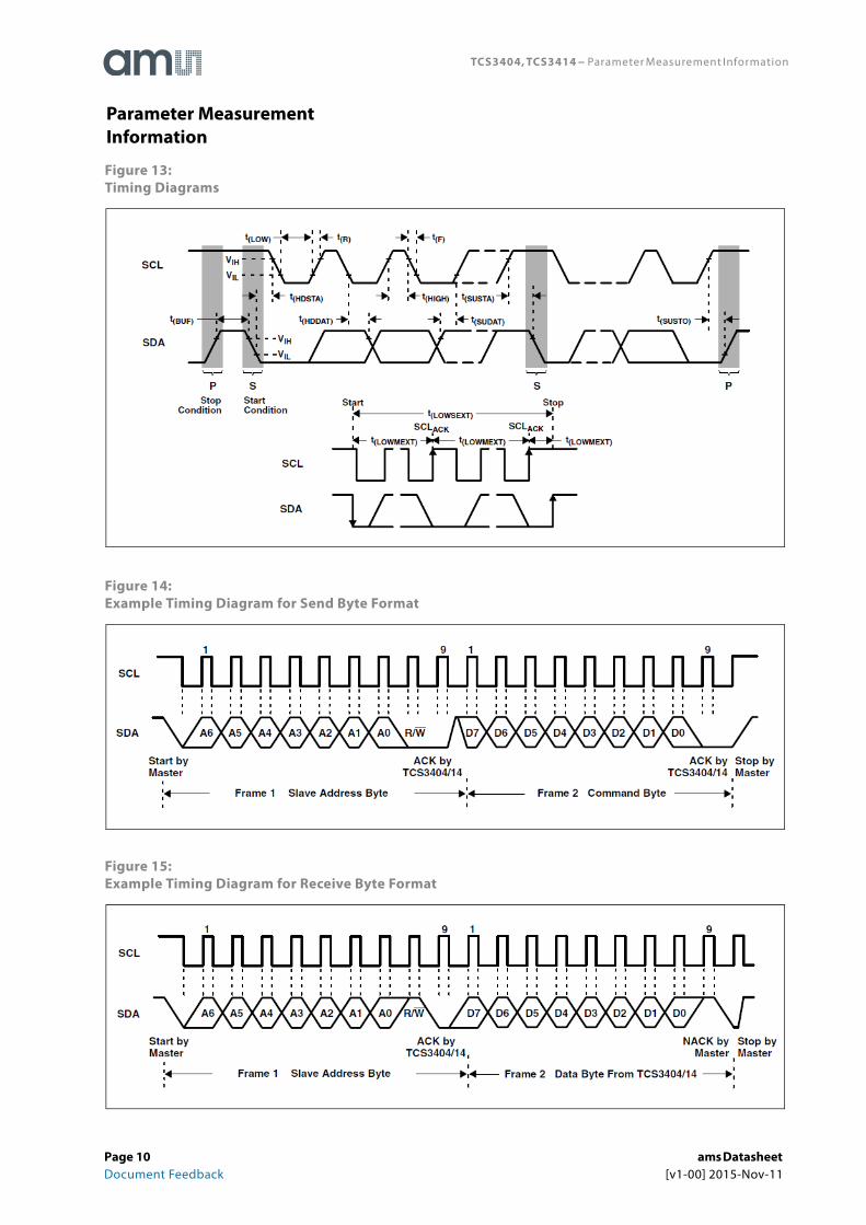
TCS3404, TCS3414 − Parameter Measurement Information
Figure 13:Timing Diagrams
Figure 14:Example Timing Diagram for Send Byte Format
Figure 15:Example Timing Diagram for Receive Byte Format
Parameter Measurement Information
Page 10 ams Datasheet Document Feedback [v1-00] 2015-Nov-11

TCS3404, TCS3414 − Typical Operating Characteristics
Figure 16:Spectral Responsivity CS Package
Figure 17:Spectral Responsivity FN Package
Spectral responsivity is normalized at 655nm.
Spectral responsivity is normalized at 850nm.
Typical Operating Characteristics
Nor
mal
ized
Res
pons
ivit
y - %
λ - Wavelength - nm
Nor
mal
ized
Res
pons
ivit
y - %
λ - Wavelength - nm
ams Datasheet Page 11[v1-00] 2015-Nov-11 Document Feedback
TCS3404, TCS3414 − Typical Operating Characteristics
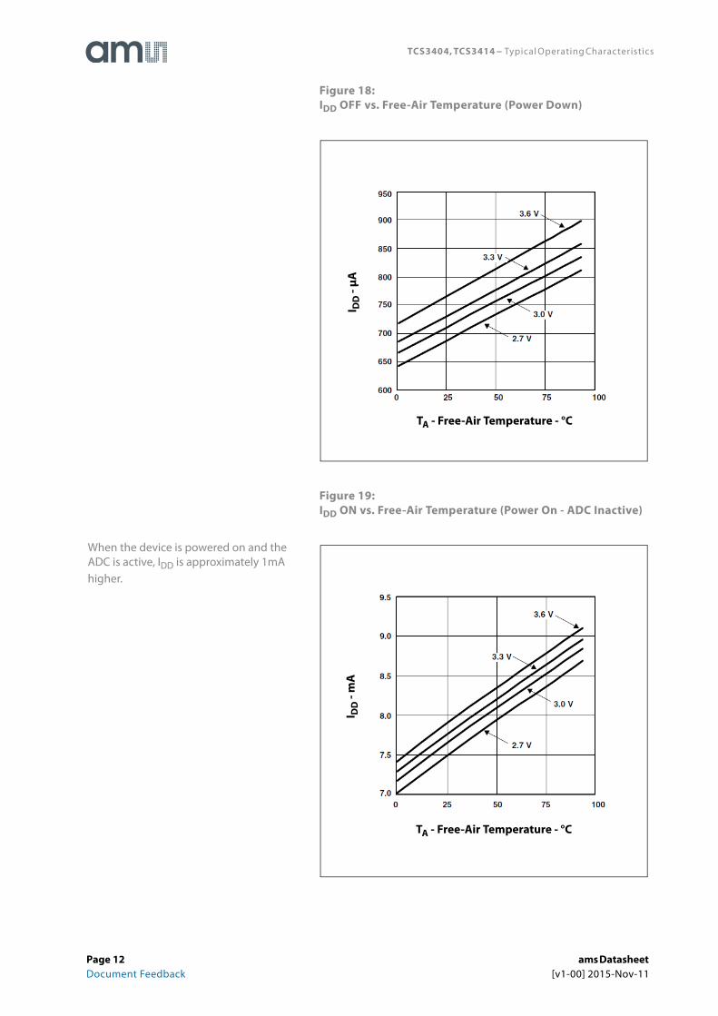
Figure 18:IDD OFF vs. Free-Air Temperature (Power Down)
Figure 19:IDD ON vs. Free-Air Temperature (Power On - ADC Inactive)
When the device is powered on and the ADC is active, IDD is approximately 1mA higher.
I DD
- μA
TA - Free-Air Temperature - °C
I DD
- m
A
TA - Free-Air Temperature - °C
Page 12 ams Datasheet Document Feedback [v1-00] 2015-Nov-11
TCS3404, TCS3414 − Typical Operating Characteristics
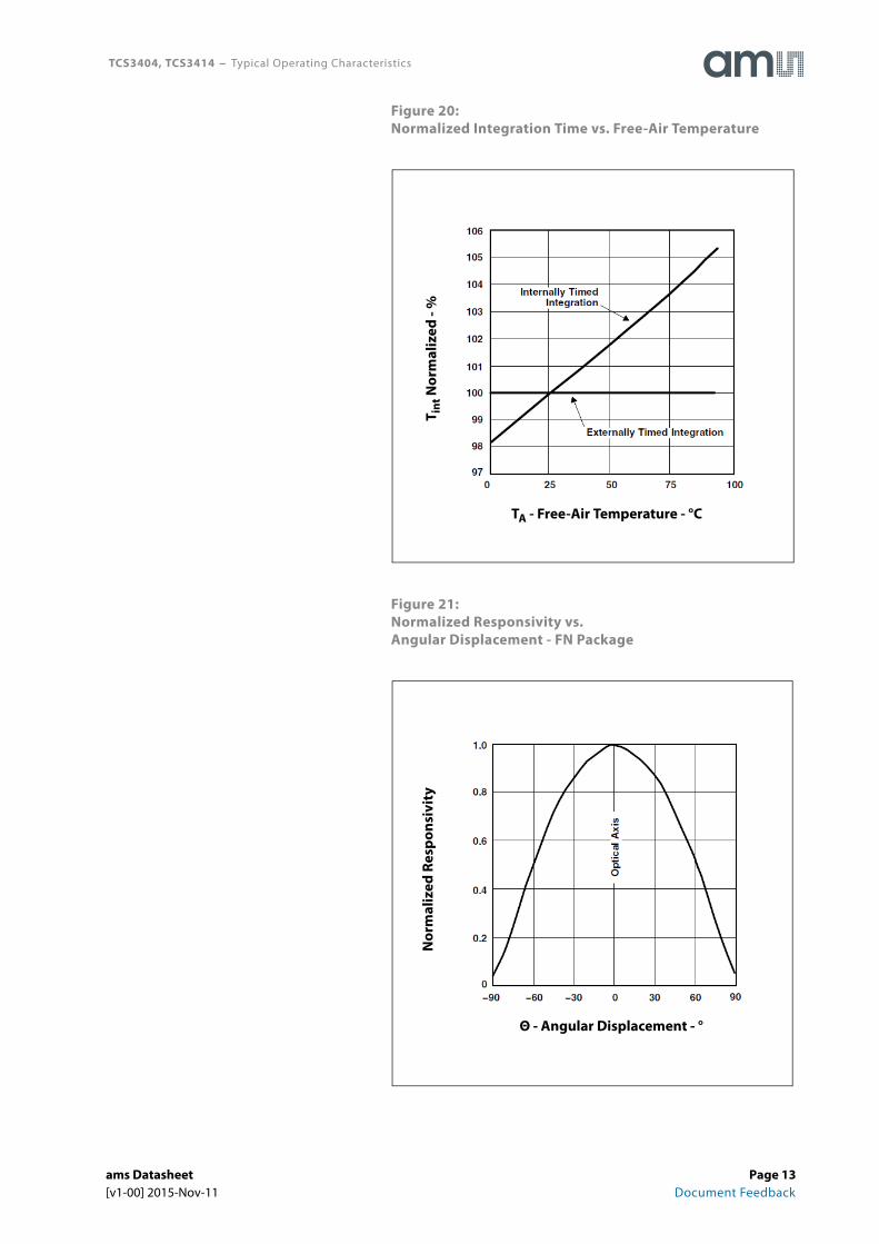
Figure 20:Normalized Integration Time vs. Free-Air Temperature
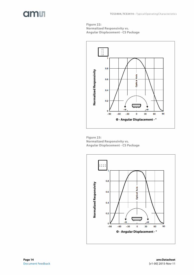
Figure 21:Normalized Responsivity vs.Angular Displacement - FN Package
T int
Nor
mal
ized
- %
TA - Free-Air Temperature - °C
Nor
mal
ized
Res
pons
ivit
y
Θ - Angular Displacement - °
ams Datasheet Page 13[v1-00] 2015-Nov-11 Document Feedback
TCS3404, TCS3414 − Typical Operating Characteristics
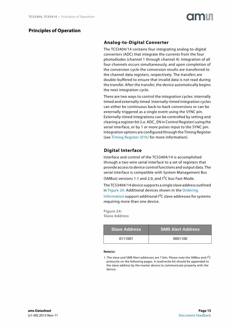
Figure 22:Normalized Responsivity vs.Angular Displacement - CS Package
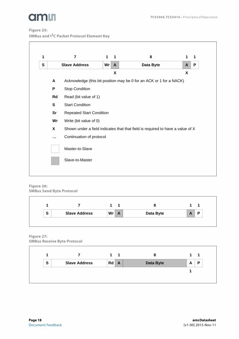
Figure 23:Normalized Responsivity vs.Angular Displacement - CS Package
Nor
mal
ized
Res
pons
ivit
y
Θ - Angular Displacement - °
Nor
mal
ized
Res
pons
ivit
y
Θ - Angular Displacement - °
Page 14 ams Datasheet Document Feedback [v1-00] 2015-Nov-11
TCS3404, TCS3414 − Principles of Operation
Analog-to-Digital ConverterThe TCS3404/14 contains four integrating analog-to-digital converters (ADC) that integrate the currents from the four photodiodes (channel 1 through channel 4). Integration of all four channels occurs simultaneously, and upon completion of the conversion cycle the conversion results are transferred to the channel data registers, respectively. The transfers are double-buffered to ensure that invalid data is not read during the transfer. After the transfer, the device automatically begins the next integration cycle.
There are two ways to control the integration cycles: internally timed and externally timed. Internally-timed integration cycles can either be continuous back-to-back conversions or can be externally triggered as a single event using the SYNC pin. Externally-timed integrations can be controlled by setting and clearing a register bit (i.e. ADC_EN in Control Register) using the serial interface, or by 1 or more pulses input to the SYNC pin. Integration options are configured through the Timing Register (see Timing Register (01h) for more information).
Digital InterfaceInterface and control of the TCS3404/14 is accomplished through a two-wire serial interface to a set of registers that provide access to device control functions and output data. The serial interface is compatible with System Management Bus
(SMBus) versions 1.1 and 2.0, and I2C bus Fast-Mode.
The TCS3404/14 device supports a single slave address outlined in Figure 24. Additional devices shown in the Ordering
Information support additional I2C slave addresses for systems requiring more than one device.
Figure 24:Slave Address
Note(s):
1. The slave and SMB Alert addresses are 7 bits. Please note the SMBus and I2C protocols on the following pages. A read/write bit should be appended to the slave address by the master device to communicate properly with the device.
Slave Address SMB Alert Address
0111001 0001100
Principles of Operation
ams Datasheet Page 15[v1-00] 2015-Nov-11 Document Feedback

TCS3404, TCS3414 − Principles of Operation
InterruptAlthough the ADC channel data registers can be read at any time to obtain the most recent conversion value, in some applications, periodic polling of the device may not be desirable. For these types of applications, the device supports a variety of interrupt options allowing the user to configure the device to signal when a change in light intensity has occurred. High and low threshold registers allow a range of light levels to be defined, outside of which the device generates an interrupt. A persistence setting allows the user to specify a time duration that the measured value must remain outside of the defined range before generating an interrupt. The interrupt function can be assigned to any one of the four ADC color channels.See Interrupt Control Register (02h) for more information on configuring the interrupt functions.
SMBus and I2C ProtocolsEach Send and Write protocol is, essentially, a series of bytes. A byte sent to the TCS3404/14 with the most significant bit (MSB) equal to 1 will be interpreted as a COMMAND byte. The lower four bits of the COMMAND byte form the register select address (see Figure 24), which is used to select the destination for the subsequent byte(s) received. The TCS3404/14 responds to any Receive Byte requests with the contents of the register specified by the stored register select address.
The TCS3404/14 implements the following protocols of the SMB 2.0 specification:
• Send Byte Protocol
• Receive Byte Protocol
• Write Byte Protocol
• Write Word Protocol
• Read Word Protocol
• Block Write Protocol
• Block Read Protocol
The TCS3404/14 implements the following protocols of the I2C specification:
• I2C Write Protocol
• I2C Read (Combined Format) Protocol
When an SMBus Block Write or Block Read is initiated(see description of Command Register), the byte following the COMMAND byte is ignored but is a requirement of the SMBus specification. This field contains the byte count (i.e. the number of bytes to be transferred). The TCS3404 (SMBus) device ignores this field and extracts this information by counting the actual number of bytes transferred before the Stop condition is detected.
Page 16 ams Datasheet Document Feedback [v1-00] 2015-Nov-11

TCS3404, TCS3414 − Principles of Operation
When an I2C Write or I2C Read (Combined Format) is initiated, the byte count is also ignored but follows the SMBus protocol specification. Data bytes continue to be transferred from the
TCS3414 (I2C) device to Master until a NACK is sent by the Master.
The data formats supported by the TCS3404 and TCS3414 devices are:
• Master transmitter transmits to slave receiver (SMBus and I2C):
• The transfer direction in this case is not changed.
• Master reads slave immediately after the first byte (SMBus only):
• At the moment of the first acknowledgment (provided by the slave receiver) the master transmitter becomes a master receiver and the slave receiver becomes a slave transmitter.
• Combined format (SMBus and I2C):• During a change of direction within a transfer, the
master repeats both a START condition and the slave address but with the R/W bit reversed. In this case, the master receiver terminates the transfer by generating a NACK on the last byte of the transfer and a STOP condition.
For a complete description of SMBus protocols, please review the SMBus Specification at www.smbus.org/specs. For a
complete description of the I2C protocol, please review the NXP
I2C design specification at www.i2c-bus.org/references.
ams Datasheet Page 17[v1-00] 2015-Nov-11 Document Feedback
TCS3404, TCS3414 − Principles of Operation
Figure 25:SMBus and I2C Packet Protocol Element Key
Figure 26:SMBus Send Byte Protocol
Figure 27:SMBus Receive Byte Protocol
S Slave Address Wr A Data Byte A P
Master-to-Slave
Slave-to-Master
… Continuation of protocol
X Shown under a field indicates that that field is required to have a value of X
Wr Write (bit value of 0)
Sr Repeated Start Condition
S Start Condition
Rd Read (bit value of 1)
P Stop Condition
A Acknowledge (this bit position may be 0 for an ACK or 1 for a NACK)
1 1 1 117 8
X X
S Slave Address Wr A Data Byte A P
1 1 1 117 8
S Slave Address Rd A Data Byte A P
1 1 1 117 8
1
Page 18 ams Datasheet Document Feedback [v1-00] 2015-Nov-11
TCS3404, TCS3414 − Principles of Operation
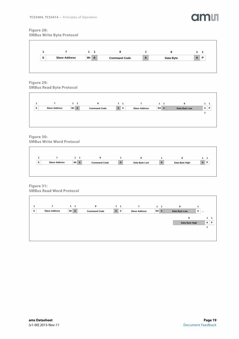
Figure 28:SMBus Write Byte Protocol
Figure 29:SMBus Read Byte Protocol
Figure 30:SMBus Write Word Protocol
Figure 31:SMBus Read Word Protocol
S Slave Address Wr A Command Code
1 1 1 17 8
A Data Byte A P
18 1
S Slave Address Wr A Command Code
1 1 1 17 8
A Slave Address Rd A
17 1
S
1
Data Byte Low A P
18 1
1
S Slave Address Wr A Command Code
1 1 1 17 8
A Data Byte Low A
8 1
Data Byte High A P
18 1
S Slave Address Wr A Command Code
1 1 1 17 8
A Slave Address Rd
7 1
Data Byte Low A
18
...S
1
A
1
Data Byte High
8
A
1
P
1
1
ams Datasheet Page 19[v1-00] 2015-Nov-11 Document Feedback
TCS3404, TCS3414 − Principles of Operation
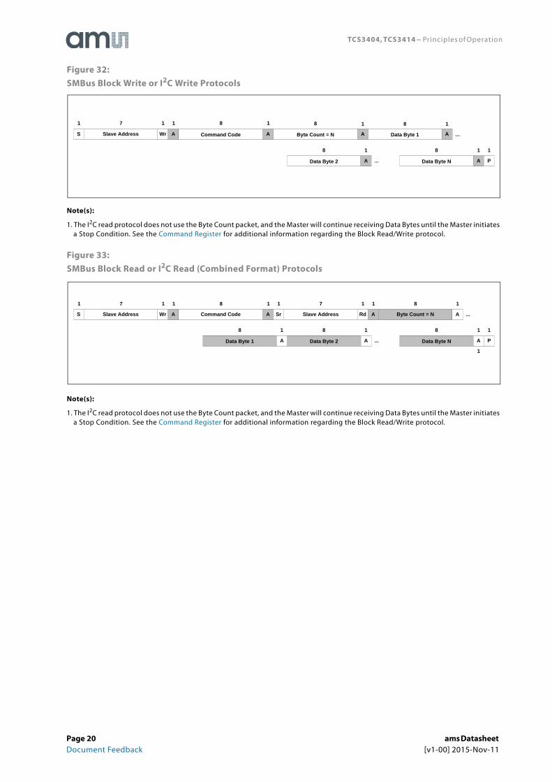
Figure 32:SMBus Block Write or I2C Write Protocols
Note(s):
1. The I2C read protocol does not use the Byte Count packet, and the Master will continue receiving Data Bytes until the Master initiates a Stop Condition. See the Command Register for additional information regarding the Block Read/Write protocol.
Figure 33:SMBus Block Read or I2C Read (Combined Format) Protocols
Note(s):
1. The I2C read protocol does not use the Byte Count packet, and the Master will continue receiving Data Bytes until the Master initiates a Stop Condition. See the Command Register for additional information regarding the Block Read/Write protocol.
S Slave Address Wr A Command Code
1 1 1 17 8
A Byte Count = N
8
Data Byte 1 A
18
...A
1
Data Byte N
8
A
1
P
1
Data Byte 2 A ...
18
S Slave Address Wr A Command Code
1 1 1 17 8
A Slave Address
7
Byte Count = N A
18
...Rd
1
Data Byte N
8
A
1
P
1
Data Byte 2 A ...
18
1
Sr A
1
1
Data Byte 1 A
18
Page 20 ams Datasheet Document Feedback [v1-00] 2015-Nov-11
TCS3404, TCS3414 − Principles of Operation
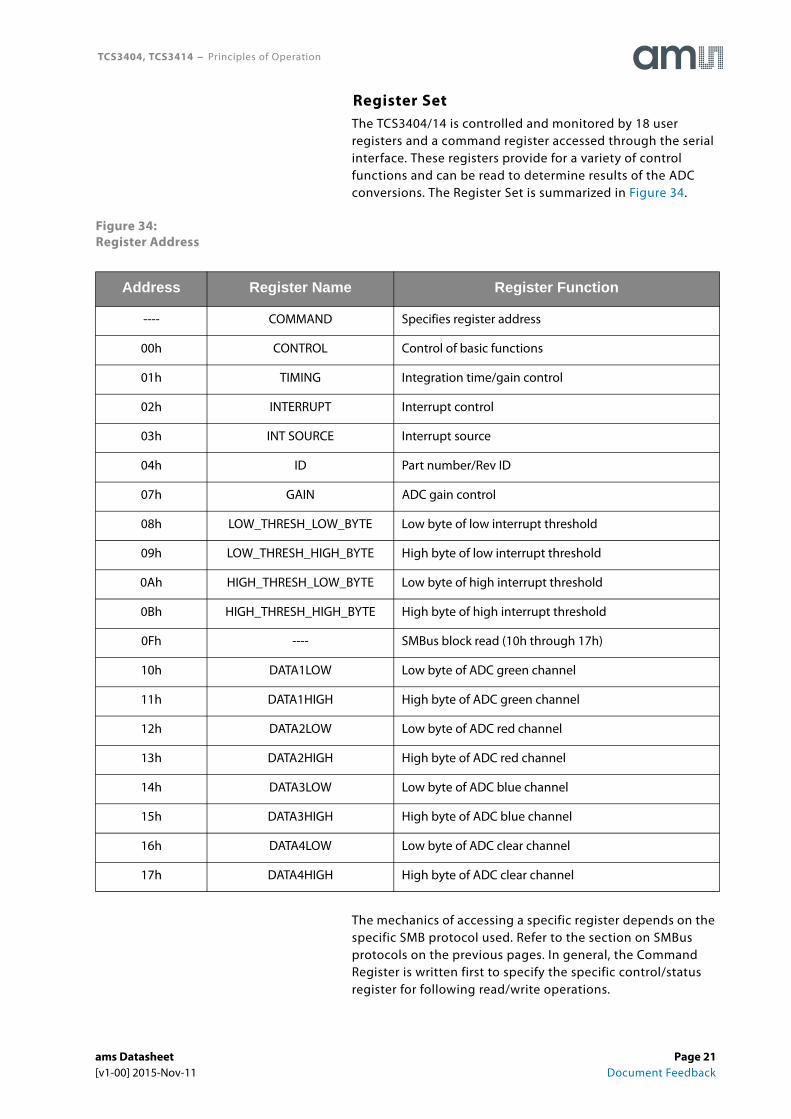
Register SetThe TCS3404/14 is controlled and monitored by 18 user registers and a command register accessed through the serial interface. These registers provide for a variety of control functions and can be read to determine results of the ADC conversions. The Register Set is summarized in Figure 34.
Figure 34:Register Address
The mechanics of accessing a specific register depends on the specific SMB protocol used. Refer to the section on SMBus protocols on the previous pages. In general, the Command Register is written first to specify the specific control/status register for following read/write operations.
Address Register Name Register Function
---- COMMAND Specifies register address
00h CONTROL Control of basic functions
01h TIMING Integration time/gain control
02h INTERRUPT Interrupt control
03h INT SOURCE Interrupt source
04h ID Part number/Rev ID
07h GAIN ADC gain control
08h LOW_THRESH_LOW_BYTE Low byte of low interrupt threshold
09h LOW_THRESH_HIGH_BYTE High byte of low interrupt threshold
0Ah HIGH_THRESH_LOW_BYTE Low byte of high interrupt threshold
0Bh HIGH_THRESH_HIGH_BYTE High byte of high interrupt threshold
0Fh ---- SMBus block read (10h through 17h)
10h DATA1LOW Low byte of ADC green channel
11h DATA1HIGH High byte of ADC green channel
12h DATA2LOW Low byte of ADC red channel
13h DATA2HIGH High byte of ADC red channel
14h DATA3LOW Low byte of ADC blue channel
15h DATA3HIGH High byte of ADC blue channel
16h DATA4LOW Low byte of ADC clear channel
17h DATA4HIGH High byte of ADC clear channel
ams Datasheet Page 21[v1-00] 2015-Nov-11 Document Feedback
TCS3404, TCS3414 − Principles of Operation
Command RegisterThe Command Register specifies the address of the target register for subsequent read and write operations. This register contains eight bits as described in Figure 35 and defaults to 00h at power on.
Figure 35:Command Register
Note(s):
1. An I2C block transaction will continue until the Master sends a stop condition. See Figure 30 and Figure 31. Unlike the I2C protocol, the TCS3404/14 SMBus read/write protocol requires a Byte Count. All eight ADC Channel Data Registers (10h through 17h) can be read simultaneously in a single SMBus transaction. This is the only 64-bit data block supported by the TCS3404 SMBus protocol. The TRANSACTION field must be set to 10, and a read condition should be initiated with a COMMAND CODE of CFh. By using a COMMAND CODE of CFh during an SMBus Block Read Protocol, the TCS3404 device will automatically insert the appropriate Byte Count (Byte Count = 8) as illustrated in Figure 30. A write condition should not be used in conjunction with the 0Fh register.
2. Only the Send Byte Protocol should be used when clearing interrupts.
7 6 5 4 3 2 1 0
CMD TRANSACTION ADDRESS
Field Bits Description
CMD 7 Select Command Register. Must write as 1.
TRANSACTION 6:5
Transaction. Selects type of transaction to follow in subsequent data transfer.
Field Value Transaction Description
00 Byte protocol SMB read/write byte protocol
01 Word protocol SMB read/write word protocol
10 Block protocol SMB read/write block protocol
11 Interrupt clearClear any pending interrupt and is a write-once-to-clear field
ADDRESS 4:0Register Address. This field selects the specific control or status register for following write and read commands according to Figure 34.
Page 22 ams Datasheet Document Feedback [v1-00] 2015-Nov-11
TCS3404, TCS3414 − Principles of Operation
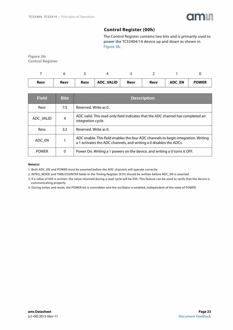
Control Register (00h)The Control Register contains two bits and is primarily used to power the TCS3404/14 device up and down as shown in Figure 36.
Figure 36:Control Register
Note(s):
1. Both ADC_EN and POWER must be asserted before the ADC channels will operate correctly.
2. INTEG_MODE and TIME/COUNTER fields in the Timing Register (01h) should be written before ADC_EN is asserted.
3. If a value of 03h is written, the value returned during a read cycle will be 03h. This feature can be used to verify that the device is communicating properly.
4. During writes and reads, the POWER bit is overridden and the oscillator is enabled, independent of the state of POWER.
7 6 5 4 3 2 1 0
Resv Resv Resv ADC_VALID Resv Resv ADC_EN POWER
Field Bits Description
Resv 7:5 Reserved. Write as 0.
ADC_VALID 4ADC valid. This read-only field indicates that the ADC channel has completed an integration cycle.
Resv 3:2 Reserved. Write as 0.
ADC_EN 1ADC enable. This field enables the four ADC channels to begin integration. Writing a 1 activates the ADC channels, and writing a 0 disables the ADCs.
POWER 0 Power On. Writing a 1 powers on the device, and writing a 0 turns it OFF.
ams Datasheet Page 23[v1-00] 2015-Nov-11 Document Feedback
TCS3404, TCS3414 − Principles of Operation
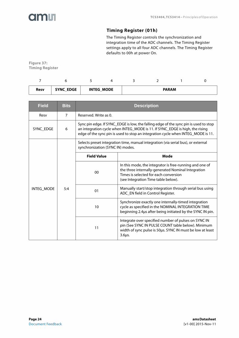
Timing Register (01h)The Timing Register controls the synchronization and integration time of the ADC channels. The Timing Register settings apply to all four ADC channels. The Timing Register defaults to 00h at power On.
Figure 37:Timing Register
7 6 5 4 3 2 1 0
Resv SYNC_EDGE INTEG_MODE PARAM
Field Bits Description
Resv 7 Reserved. Write as 0.
SYNC_EDGE 6Sync pin edge. If SYNC_EDGE is low, the falling edge of the sync pin is used to stop an integration cycle when INTEG_MODE is 11. If SYNC_EDGE is high, the rising edge of the sync pin is used to stop an integration cycle when INTEG_MODE is 11.
INTEG_MODE 5:4
Selects preset integration time, manual integration (via serial bus), or external synchronization (SYNC IN) modes.
Field Value Mode
00
In this mode, the integrator is free-running and one of the three internally-generated Nominal Integration Times is selected for each conversion(see Integration Time table below).
01Manually start/stop integration through serial bus using ADC_EN field in Control Register.
10Synchronize exactly one internally-timed integration cycle as specified in the NOMINAL INTEGRATION TIME beginning 2.4μs after being initiated by the SYNC IN pin.
11
Integrate over specified number of pulses on SYNC IN pin (See SYNC IN PULSE COUNT table below). Minimum width of sync pulse is 50μs. SYNC IN must be low at least 3.6μs.
Page 24 ams Datasheet Document Feedback [v1-00] 2015-Nov-11
TCS3404, TCS3414 − Principles of Operation
Note(s):
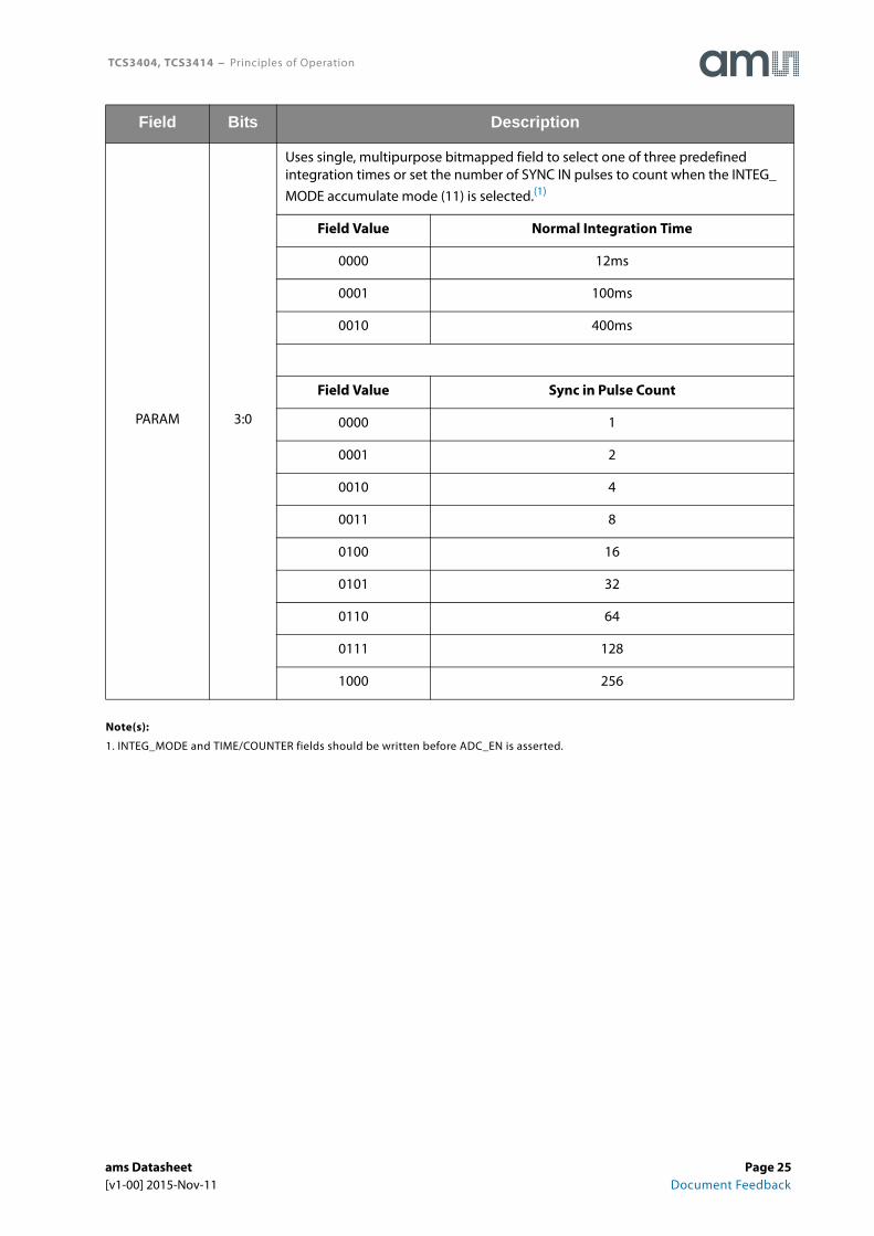
1. INTEG_MODE and TIME/COUNTER fields should be written before ADC_EN is asserted.
PARAM 3:0
Uses single, multipurpose bitmapped field to select one of three predefined integration times or set the number of SYNC IN pulses to count when the INTEG_MODE accumulate mode (11) is selected.(1)
Field Value Normal Integration Time
0000 12ms
0001 100ms
0010 400ms
Field Value Sync in Pulse Count
0000 1
0001 2
0010 4
0011 8
0100 16
0101 32
0110 64
0111 128
1000 256
Field Bits Description
ams Datasheet Page 25[v1-00] 2015-Nov-11 Document Feedback
TCS3404, TCS3414 − Principles of Operation
Interrupt Control Register (02h)The Interrupt Register controls the extensive interrupt capabilities of the device. The open-drain interrupt pin is active low and requires a pullup resistor to VDD in order to pull high in the inactive state. Using the Interrupt Source Register (03h), the interrupt can be configured to trigger on any one of the four ADC channels. The TCS3404/14 permits both SMB-Alert style interrupts as well as traditional level style interrupts. The Interrupt Register provides control over when a meaningful interrupt will occur. The concept of a meaningful change can be defined by the user both in terms of light intensity and time, or persistence of that change in intensity. The value must cross the threshold (as configured in the Threshold Registers 08h through 0Bh) and persist for some period of time as outlined in the table below.
When a level Interrupt is selected, an interrupt is generated whenever the last conversion results in a value outside of the programmed threshold window. The interrupt is active-low and remains asserted until cleared by writing an 11 in the TRANSACTION field in the Command Register.
In SMB-Alert mode, the interrupt is similar to the traditional level style and the interrupt line is asserted low. To clear the interrupt, the host responds to the SMB-Alert by performing a modified Receive Byte operation, in which the Alert Response Address (ARA) is placed in the slave address field, and the TCS3404/14 that generated the interrupt responds by returning its own address in the seven most significant bits of the receive data byte. If more than one device connected on the bus has pulled the SMBAlert line low, the highest priority (lowest address) device will win control of the bus during the slave address transfer. If the device loses this arbitration, the interrupt will not be cleared. The Alert Response Address is 0Ch.
When INTR = 11, the interrupt is generated immediately following the SMBus write operation. Operation then behaves in an SMB-Alert mode, and the software set interrupt may be cleared by an SMB-Alert cycle.
Page 26 ams Datasheet Document Feedback [v1-00] 2015-Nov-11
TCS3404, TCS3414 − Principles of Operation
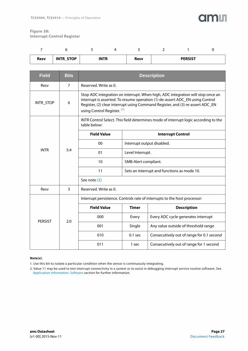
Figure 38:Interrupt Control Register
Note(s):
1. Use this bit to isolate a particular condition when the sensor is continuously integrating.
2. Value 11 may be used to test interrupt connectivity in a system or to assist in debugging interrupt service routine software. See Application Information: Software section for further information.
7 6 5 4 3 2 1 0
Resv INTR_STOP INTR Resv PERSIST
Field Bits Description
Resv 7 Reserved. Write as 0.
INTR_STOP 6
Stop ADC integration on interrupt. When high, ADC integration will stop once an interrupt is asserted. To resume operation (1) de-assert ADC_EN using Control Register, (2) clear interrupt using Command Register, and (3) re-assert ADC_EN using Control Register. (1)
INTR 5:4
INTR Control Select. This field determines mode of interrupt logic according to the table below:
Field Value Interrupt Control
00 Interrupt output disabled.
01 Level Interrupt.
10 SMB-Alert compliant.
11 Sets an interrupt and functions as mode 10.
See note (2)
Resv 3 Reserved. Write as 0.
PERSIST 2:0
Interrupt persistence. Controls rate of interrupts to the host processor:
Field Value Timer Description
000 Every Every ADC cycle generates interrupt
001 Single Any value outside of threshold range
010 0.1 sec Consecutively out of range for 0.1 second
011 1 sec Consecutively out of range for 1 second
ams Datasheet Page 27[v1-00] 2015-Nov-11 Document Feedback

TCS3404, TCS3414 − Principles of Operation
Interrupt Source Register (03h)The Interrupt Source Register selects which ADC channel value to use to generate an interrupt. Only one of the four ADC channels can be selected.
Figure 39:Interrupt Source Register
Note(s):
1. The INTERRUPT THRESHOLD Register (08h−0Bh) should be configured appropriately to correspond to the ADC channel value that generates an interrupt.
ID Register (04h)The ID Register provides the value for both the part number and silicon revision number for that part number. It is a read-only register, whose value never changes.
Figure 40:ID Register
7 6 5 4 3 2 1 0
Resv Resv Resv Resv Resv Resv INT SOURCE
Field Bits Description
Resv 7:2 Reserved. Write as 0.
INT SOURCE 1:0
Interrupt Source. Selects which ADC channel to use to generate an interrupt:
Field Value Interrupt Source
00 Green channel
01 Red channel
10 Blue channel
11 Clear channel
7 6 5 4 3 2 1 0
PARTNO REVNO
Field Bits Description
PARTNO 7:4Part Number Identification: field value 0000 = TCS3404field value 0001 = TCS3413, TCS3414, TCS3415, and TCS3416
REVNO 3:0 Revision number identification
Page 28 ams Datasheet Document Feedback [v1-00] 2015-Nov-11

TCS3404, TCS3414 − Principles of Operation
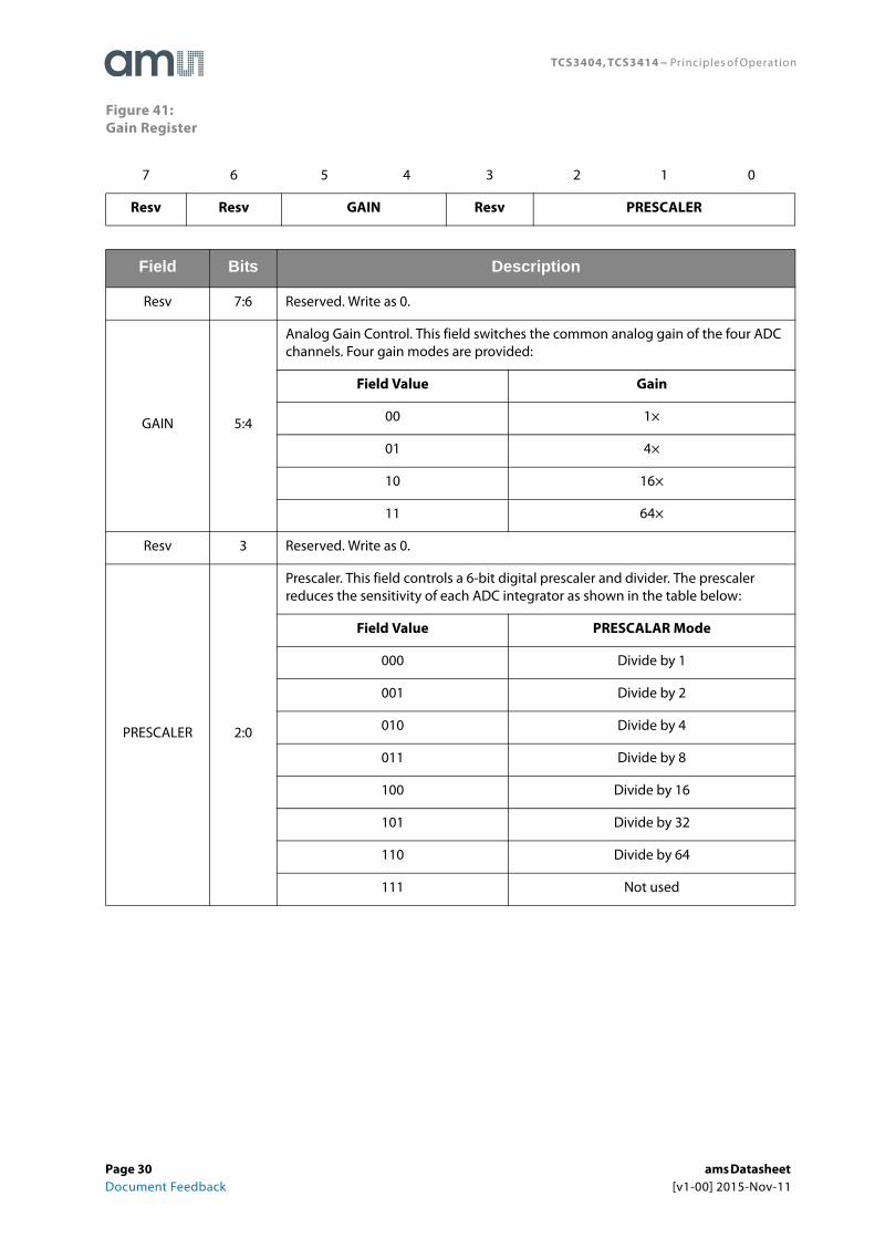
Gain Register (07h)The Gain Register provides a common gain control adjustment for all four parallel ADC output channels. Two gain bits [5:4] in the Gain Register allow the relative gain to be adjusted from 1× to 64× in 4× increments. The advantage of the gain adjust is to extend the dynamic range of the light input up to a factor of 64× before analog or digital saturation occurs. If analog saturation has occurred, lowering the gain sensitivity will likely prevent analog saturation especially when the integration time is relatively short. For longer integration times, the 16-bit output could be in digital saturation (64K). If lowering the gain to 1× does not prevent digital saturation from occurring, the use of PRESCALER can be useful.
The PRESCALER is 3 bits [2:0] in the Gain Register that divides down the output count (i.e. shifts the LSB of the count value to the right). The PRESCALER adjustment range is divide by 1 to 64 in multiples of 2.
The most sensitive gain setting of the device would be when GAIN is set to 11b (64×), and PRESCALER is set to 000b (divide by 1). The least sensitive part setting would be GAIN 00 (1×) and PRESCALER 110 (divide by 64). If the part continues to be in digital saturation at the least sensitive setting, the integration time can be lowered (see Timing Register (01h) section).
ams Datasheet Page 29[v1-00] 2015-Nov-11 Document Feedback
TCS3404, TCS3414 − Principles of Operation
Figure 41:Gain Register
7 6 5 4 3 2 1 0
Resv Resv GAIN Resv PRESCALER
Field Bits Description
Resv 7:6 Reserved. Write as 0.
GAIN 5:4
Analog Gain Control. This field switches the common analog gain of the four ADC channels. Four gain modes are provided:
Field Value Gain
00 1×
01 4×
10 16×
11 64×
Resv 3 Reserved. Write as 0.
PRESCALER 2:0
Prescaler. This field controls a 6-bit digital prescaler and divider. The prescaler reduces the sensitivity of each ADC integrator as shown in the table below:
Field Value PRESCALAR Mode
000 Divide by 1
001 Divide by 2
010 Divide by 4
011 Divide by 8
100 Divide by 16
101 Divide by 32
110 Divide by 64
111 Not used
Page 30 ams Datasheet Document Feedback [v1-00] 2015-Nov-11

TCS3404, TCS3414 − Principles of Operation
Interrupt Threshold Register (08h - 0Bh)The Interrupt Threshold Registers store the values to be used as the high and low trigger points for the comparison function for interrupt generation. The high and low bytes from each set of registers are combined to form a 16-bit threshold value. If the value generated by the Interrupt Source Register (03h) converges below or equal to the low threshold specified, an interrupt is asserted on the interrupt pin. If the value generated by Interrupt Source Register (03h) converges above the high threshold specified, an interrupt is asserted on the interrupt pin. Registers LOW_THRESH_LOW_BYTE and LOW_THRESH_HIGH_BYTE provide the low byte and high byte, respectively, of the lower interrupt threshold. Registers HIGH_THRESH_LOW_BYTE and HIGH_THRESH_HIGH_BYTE provide the low and high bytes, respectively, of the upper interrupt threshold. The Interrupt Threshold Registers default to 00h on power up.
Figure 42:Interrupt Threshold Register
Note(s):
1. The Interrupt Source Register (03h) selects which ADC channel to generate an interrupt and should correspond to the threshold setting. Both registers should be configured appropriately when setting up an interrupt service routine.
2. Since two 8-bit values are combined for a single 16-bit value for each of the high and low interrupt thresholds, the SMBus Send Byte protocol should not be used to write to these registers. Any values transferred by the Send Byte protocol with the MSB set would be interpreted as the COMMAND field and stored as an address for subsequent read/write operations and not as the interrupt threshold information as desired. The Write Word protocol should be used to write byte-paired registers. For example, the LOW_THRESH_LOW_BYTE and LOW_THRESH_HIGH_BYTE registers (as well as the HIGH_THRESH_LOW_BYTE and HIGH_THRESH_HIGH_BYTE registers) can be written together to set the 16-bit ADC value in a single transaction.
Register Address Bits Description
LOW_THRESH_LOW_BYTE 08h 7:0 ADC interrupt source lower byte of the low threshold
LOW_THRESH_HIGH_BYTE 09h 7:0 ADC interrupt source upper byte of the low threshold
HIGH_THRESH_LOW_BYTE 0Ah 7:0 ADC interrupt source lower byte of the high threshold
HIGH_THRESH_HIGH_BYTE 0Bh 7:0 ADC interrupt source upper byte of the high threshold
ams Datasheet Page 31[v1-00] 2015-Nov-11 Document Feedback
TCS3404, TCS3414 − Principles of Operation
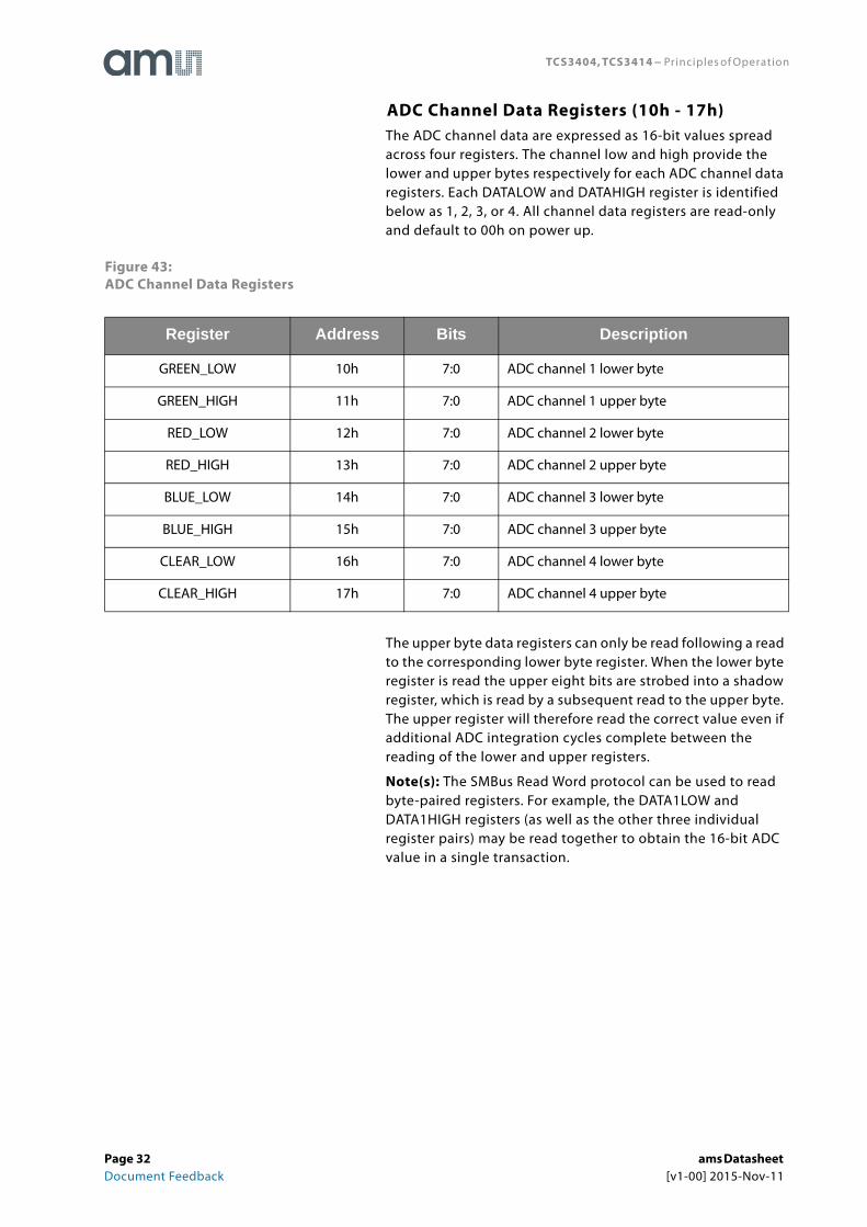
ADC Channel Data Registers (10h - 17h)The ADC channel data are expressed as 16-bit values spread across four registers. The channel low and high provide the lower and upper bytes respectively for each ADC channel data registers. Each DATALOW and DATAHIGH register is identified below as 1, 2, 3, or 4. All channel data registers are read-only and default to 00h on power up.
Figure 43:ADC Channel Data Registers
The upper byte data registers can only be read following a read to the corresponding lower byte register. When the lower byte register is read the upper eight bits are strobed into a shadow register, which is read by a subsequent read to the upper byte. The upper register will therefore read the correct value even if additional ADC integration cycles complete between the reading of the lower and upper registers.
Note(s): The SMBus Read Word protocol can be used to read byte-paired registers. For example, the DATA1LOW and DATA1HIGH registers (as well as the other three individual register pairs) may be read together to obtain the 16-bit ADC value in a single transaction.
Register Address Bits Description
GREEN_LOW 10h 7:0 ADC channel 1 lower byte
GREEN_HIGH 11h 7:0 ADC channel 1 upper byte
RED_LOW 12h 7:0 ADC channel 2 lower byte
RED_HIGH 13h 7:0 ADC channel 2 upper byte
BLUE_LOW 14h 7:0 ADC channel 3 lower byte
BLUE_HIGH 15h 7:0 ADC channel 3 upper byte
CLEAR_LOW 16h 7:0 ADC channel 4 lower byte
CLEAR_HIGH 17h 7:0 ADC channel 4 upper byte
Page 32 ams Datasheet Document Feedback [v1-00] 2015-Nov-11
TCS3404, TCS3414 − Application Information: Software
Basic OperationAfter applying VDD, the device will initially be in the power−down state. To operate the device, issue a command to access the control register followed by the data value 03h to the control register to set ADC_EN and POWER to power up the device. At this point, all four ADC channels will begin a conversion at the default integration time of 12ms. After 12ms, the conversion results will be available in ADC Channel Data Registers (10h through 17h). The following pseudo code illustrates a procedure for reading the TCS3404/14 device using Word and Byte transactions:
// Read ADC Channels Using Read Word Protocol − RECOMMENDED
Address = 0x39
Command = 0x80
PowerUp = 0x03 //Power Up and Enable ADC
//Wait for integration conversion
//Address the Ch1 lower data register and configure for Read Word
Command = 0xB0 //Set Command bit and Word transaction
//Reads two bytes from sequential registers 10h and 11h
//Results are returned in DataLow and DataHigh variables
ReadWord (Address, Command, DataLow, DataHigh)
Channel1 = 256 * DataHigh + DataLow
//Address the Ch2 lower data register and configure for Read Word
Command = 0xB2 //Set Command bit and Word transaction
//Reads two bytes from sequential registers 12h and 13h
//Results are returned in DataLow and DataHigh variables
ReadWord (Address, Command, DataLow, DataHigh)
Channel2 = 256 * DataHigh + DataLow //Shift DataHigh to upper byte
//Address the Ch3 lower data register and configure for Read Word
Command = 0xB4 //Set Command bit and Word transaction
//Reads two bytes from sequential registers 14h and 15h
//Results are returned in DataLow and DataHigh variables
ReadWord (Address, Command, DataLow, DataHigh)
Channel3 = 256 * DataHigh + DataLow
//Address the Ch4 lower data register and configure for Read Word
Command = 0xB6 //Set Command bit and Word transaction
//Reads two bytes from sequential registers 16h and 17h
//Results are returned in DataLow and DataHigh variables
ReadWord (Address, Command, DataLow, DataHigh)
Channel4 = 256 * DataHigh + DataLow //Shift DataHigh to upper byte
Application Information: Software
ams Datasheet Page 33[v1-00] 2015-Nov-11 Document Feedback
TCS3404, TCS3414 − Application Information: Software
// Read ADC Channels Using Read Byte Protocol
Address = 0x39 //Slave addr − also 0x29 or 0x49
Command = 0x90 //Address the Ch1 lower data register
ReadByte (Address, Command, DataLow) //Result returned in DataLow
Command = 0x91 //Address the Ch1 upper data register
ReadByte (Address, Command, DataHigh) //Result returned in DataHigh
Channel1 = 256 * DataHigh + DataLow //Shift DataHigh to upper byte
Command = 0x92 //Address the Ch2 lower data register
ReadByte (Address, Command, DataLow) //Result returned in DataLow
Command = 0x93 //Address the Ch2 upper data register
ReadByte (Address, Command, DataHigh) //Result returned in DataHigh
Channel2 = 256 * DataHigh + DataLow //Shift DataHigh to upper byte
Command = 0x94 //Address the Ch3 lower data register
ReadByte (Address, Command, DataLow) //Result returned in DataLow
Command = 0x95 //Address the Ch3 upper data register
ReadByte (Address, Command, DataHigh) //Result returned in DataHigh
Channel3 = 256 * DataHigh + DataLow //Shift DataHigh to upper byte
Command = 0x96 //Address the Ch4 lower data register
ReadByte (Address, Command, DataLow) //Result returned in DataLow
Command = 0x97 //Address the Ch4 upper data register
ReadByte (Address, Command, DataHigh) //Result returned in DataHigh
Channel4 = 256 * DataHigh + DataLow //Shift DataHigh to upper byte
Page 34 ams Datasheet Document Feedback [v1-00] 2015-Nov-11
TCS3404, TCS3414 − Application Information: Software
Configuring the Timing RegisterThe command, timing, and control registers are initialized to default values on power up. Setting these registers to the desired values would be part of a normal initialization or setup procedure. In addition, to maximize the performance of the device under various conditions, the integration time and gain may be changed often during operation. The following pseudo code illustrates a procedure for setting up the timing register for various options.
// Set up Timing Register
//Low Gain (1x), integration time of 12ms (default value)
Address = 0x39
Command = 0x81 //Timing Register
Data = 0x02
WriteByte (Address, Command, Data)
//Low Gain (1x), integration time of 101ms
Command = 0x81 //Timing Register
Data = 0x01
WriteByte (Address, Command, Data)
//Low Gain (1x), integration time of 12ms
Data = 0x00
WriteByte (Address, Command, Data)
//High Gain (16x), integration time of 101ms
Command = 0x81 //Timing Register
Data = 0x01
WriteByte (Address, Command, Data)
Command = 0x87 //Gain Control Register
Data = 0x20
WriteByte (Address, Command, Data)
//Read data registers (see Basic Operation example)
//Perform Manual Integration of 50 us
//Set up for manual integration
Command = 0x80
Data = 0x01 //Disable ADC_EN
WriteByte (Address, Command, Data)
Command = 0x81
Data = 0x10 //Set manual integration
WriteByte (Address, Command, Data)
Command = 0x80
Data = 0x03 //Enable ADC_EN and begin integration
WriteByte (Address, Command, Data)
//Integrate for 50ms
Sleep (50) //Wait for 50ms
ams Datasheet Page 35[v1-00] 2015-Nov-11 Document Feedback
TCS3404, TCS3414 − Application Information: Software
//Stop integrating
Command 0x80
Data = 0x01 //Disable ADC_EN and stop integration
WriteByte(Address, Command, Data)
//Read data registers (see Basic Operation example)
SynchronizationThere are two basic modes of operation for controlling synchronization: (1) internally timed, and (2) externally timed. Internally-timed integration cycles can either be continuous back-to-back conversions or can be externally triggered as a single event using the SYNC pin. Externally-timed integrations can be controlled by setting and clearing the ADC Enable in the Control Register using the serial interface, or by one or more pulses input to the SYNC pin. Internally-timed integration cycle times are dependent on the PARAM field value and the internal clock frequency. Nominal integration times and respective scaling between integration times scale proportionally as shown in the PARAM field in Figure 37. See Operating Characteristics Table notes for detailed information regarding how the scale values were obtained.
If a particular integration time period is required that is not listed in the PARAM Integration Time field value, then the manual timing control feature can be used to manually start and stop the integration time period by settingINTEG_MODE=01b. Manual integration is performed as follows:
Figure 44:Manual Integration (INTEG_MODE 01b)
1. Disable ADC_EN (= 0) before initiating a manual integration cycle
2. Clear and enable INTR before each cycle
3. Write 01b to INTEG_MODE field
4. Set ADC_EN (= 1) to start integration
5. Clear ADC_EN (= 0) to stop integration
6. Read channel data
Page 36 ams Datasheet Document Feedback [v1-00] 2015-Nov-11
TCS3404, TCS3414 − Application Information: Software
When the INTEG_MODE field value is set to 10b, an externally-controlled synchronization input (SYNC) is used to trigger the start of an integration period. The integration period starts on the rising edge of the SYNC pulse, triggers a single, internally-timed integration cycle, and continues until the Nominal Integration Time, as defined in the PARAM field, is completed.
Figure 45:One-Shot Integration (INTEG_MODE 10b) Falling Edge
Note(s):
1. ADC_EN must be toggled (i.e. from high to low and back to high again) before next integration cycle
1. Enable ADC_EN (= 1)
2. Set PARAM for desired integration cycle(12ms, 100ms, or 400ms)
3. Set INTEG_MODE to 10b
4. Disable SYNC and clear INTR
5. Read channel data
When the INTEG_MODE field value is set to 11b, the device integrates from the rising edge of the first pulse until the rising or falling edge of a subsequent pulse as specified by the SYNC_EDGE and PARAM field values. See example timing diagrams below. ADC_EN must be toggled (i.e. from high to low and back to high again) before the next integration cycle. With this device feature, the SYNC IN input pin can be used to synchronize the device with an external light source (e.g. LED).
ams Datasheet Page 37[v1-00] 2015-Nov-11 Document Feedback
TCS3404, TCS3414 − Application Information: Software
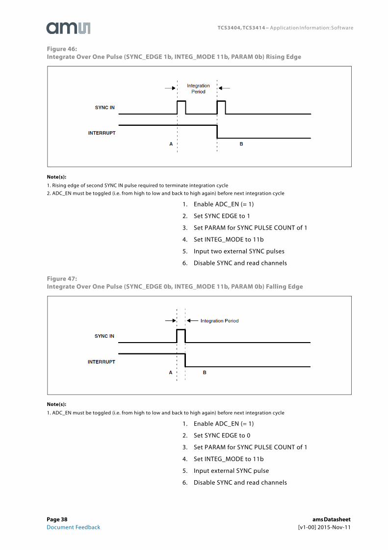
Figure 46:Integrate Over One Pulse (SYNC_EDGE 1b, INTEG_MODE 11b, PARAM 0b) Rising Edge
Note(s):
1. Rising edge of second SYNC IN pulse required to terminate integration cycle
2. ADC_EN must be toggled (i.e. from high to low and back to high again) before next integration cycle
1. Enable ADC_EN (= 1)
2. Set SYNC EDGE to 1
3. Set PARAM for SYNC PULSE COUNT of 1
4. Set INTEG_MODE to 11b
5. Input two external SYNC pulses
6. Disable SYNC and read channels
Figure 47:Integrate Over One Pulse (SYNC_EDGE 0b, INTEG_MODE 11b, PARAM 0b) Falling Edge
Note(s):
1. ADC_EN must be toggled (i.e. from high to low and back to high again) before next integration cycle
1. Enable ADC_EN (= 1)
2. Set SYNC EDGE to 0
3. Set PARAM for SYNC PULSE COUNT of 1
4. Set INTEG_MODE to 11b
5. Input external SYNC pulse
6. Disable SYNC and read channels
Page 38 ams Datasheet Document Feedback [v1-00] 2015-Nov-11

TCS3404, TCS3414 − Application Information: Software
Figure 48:Integrate Over Two Pulses (SYNC_EDGE 1b, INTEG_MODE 11b, PARAM Xb) Rising Edge
Note(s):
1. Rising edge of third SYNC IN pulse required to terminate integration cycle
2. ADC_EN must be toggled (i.e. from high to low and back to high again) before next integration cycle
1. Enable ADC_EN (= 1)
2. Set SYNC EDGE to 1
3. Set PARAM for desired SYNC PULSE COUNT
4. Set INTEG_MODE to 11b
5. Input N+1 external SYNC pulses
6. Disable SYNC and read channels
Figure 49:Integrate Over Two Pulses (SYNC_EDGE 0b, INTEG_MODE 11b, PARAM Xb) Falling Edge
Note: ADC_EN must be toggled (i.e. from high to low and back to high again) before next integration cycle
1. Enable ADC_EN (= 1)
2. Set SYNC EDGE to 0
3. Set PARAM for desired SYNC PULSE COUNT
4. Set INTEG_MODE to 11b
5. Input N external SYNC pulse(s)
6. Disable SYNC and read channels
ams Datasheet Page 39[v1-00] 2015-Nov-11 Document Feedback
TCS3404, TCS3414 − Application Information: Software
A synchronization input (SYNC IN) is supported to precisely start/stop sensor integration and synchronize with the light source. The TIMING Register (01h) provides two synchronization modes of operation. The first mode of operation synchronizes the SYNC IN pin for one integration cycle as specified in the Timing Register (01h). When the rising edge of the signal is detected, the TCS3404/14 begins integration. The second mode accumulates a specified number of SYNC IN pulses (see Timing Register (01h)) in which the minimum pulse width is 50μs. A pulse counter is used to count the rising and falling edges of the pulse(s) and precisely integrate the light level when the SYNC IN pulse is high.
The following pseudo code illustrates a procedure for reading the TCS3404/14 device using the synchronization feature:
// Synchronize one integration cycle
// See ”Basic Operation” to power−on and start device
// See ”Configuring the Timing Register” to setup environment
Address = 0x39 //Slave addr − also 0x29 or 0x49
Command = 0x81 //Set Command bit and address Timing Register
Data = 0x21 //Sync one 100ms integration period
//External SYNC IN pulse initiates 100ms integration
Sleep (100)
// See ”Basic Operation” to read Data Registers using Byte or Word Protocol
// Synchronize N number of SYNC IN pulses
// See ”Basic Operation” to power−on and start device
// See ”Configuring the Timing Register” to setup environment
Address = 0x39 //Slave addr − also 0x29 or 0x49
Command = 0x81 //Set Command bit and address Timing Register
Data = 0x30 //Integrate one SYNC IN pulse
//External SYNC IN pulse synchronizes integration
// See ”Basic Operation” to read Data Registers using Byte or Word Protocol
Page 40 ams Datasheet Document Feedback [v1-00] 2015-Nov-11
TCS3404, TCS3414 − Application Information: Software
InterruptsThe interrupt feature of the TCS3404/14 device simplifies and improves system efficiency by eliminating the need to poll the sensor for a light intensity value. Interrupt mode is determined by the INTR field in the Interrupt Control Register. The interrupt feature may be disabled by writing a field value of 00h to the Interrupt Control Register (02h) so that polling can be performed.
The versatility of the interrupt feature provides many options for interrupt configuration and usage. The primary purpose of the interrupt function is to signal a meaningful change in light intensity. However, it also be used as an end-of-conversion signal. The concept of a meaningful change can be defined by the user both in terms of light intensity and time, or persistence, of that change in intensity. The TCS3404/14 device implements two 16-bit-wide interrupt threshold registers that allow the user to define thresholds above and below a desired light level. An interrupt will then be generated when the value of a conversion exceeds either of these limits. For simplicity of programming, the threshold comparison uses the Interrupt Source Register (03h) to select which ADC channel(1 through 4) to generate the interrupt. This simplifies calculation of thresholds that are based on a percent of the current light level. For example, it is adequate to use only one channel (e.g. green channel) when calculating light intensity differences since, for a given light source, channel values are linearly proportional to each other and thus each value scales linearly with light intensity.
To further control when an interrupt occurs, the TCS3404/14 device provides an interrupt persistence feature. This feature allows the user to specify the length in time of the number of consecutive ADC channel values for which a light intensity exceeding either interrupt threshold must persist before actually generating an interrupt. This can be used to prevent transient changes in light intensity from generating an unwanted interrupt. See Figure 38 regarding the number of timer values provided.
Two different interrupt styles are available: Level and SMBus Alert. The difference between these two interrupt styles is how they are cleared. Both result in the interrupt line going active low and remaining low until the interrupt is cleared. A level style interrupt is cleared by setting the Interrupt Clear field in the COMMAND register to 11b. The SMBus Alert style interrupt is cleared by an Alert Response as described in the Interrupt Control Register section and SMBus specification.
To configure the interrupt as an end−of−conversion signal so that every ADC integration cycle generates an interrupt, the interrupt PERSIST field in the Interrupt Control Register (02h) is set to 000b. Either Level or SMBus Alert style can be used.
ams Datasheet Page 41[v1-00] 2015-Nov-11 Document Feedback
TCS3404, TCS3414 − Application Information: Software
An interrupt will be generated upon completion of each conversion. The interrupt threshold registers are ignored. The following example illustrates the configuration of a level interrupt:
// Set up end−of−conversion interrupt, Level style
Address = 0x39 //Slave address − alternatively 0x29 or 0x49
Command = 0x83 //Interrupt Source Register
Data = 0x01 //Select Channel 2
WriteByte (Address, Command, Data)
Command = 0x82 //Address Interrupt Register
Data = 0x10 //Level style, every ADC cycle
WriteByte (Address, Command, Data)
The following example pseudo code illustrates the configuration of an SMB-Alert style interrupt when the light intensity changes 20% from the current value, and persists for 2.5 seconds:
//Assume Interrupt Source as Channel 1
//Read current light level
Address = 0x39 //Slave address − alternatively 0x29 or 0x49
Command = 0xB0 //Set Command bit and SMBus Word read
ReadWord (Address, Command, DataLow, DataHigh)
Channel1 = (256 * DataHigh) + DataLow
//Calculate upper and lower thresholds
T_Upper = Channel1 + (0.2 * Channel1)
T_Lower = Channel1 − (0.2 * Channel1)
//Write the lower threshold register
Command = 0xA8 //Address lower threshold register, set Word Bit
WriteWord (Address, Command, T_Lower.LoByte, T_Lower.HiByte)
//Write the upper threshold register
Command = 0xAA //Address upper threshold register, set Word bit
WriteWord (Address, Command, T_Upper.LoByte, T_Upper.HiByte)
//Enable interrupt
Command = 0x82 //Address interrupt register
Data = 0x24 //SMBAlert style, Persist 2.5 seconds
WriteByte (Address, Command, Data)
In order to generate an interrupt on demand during system test or debug, a test mode (INTR = 11) can be used. The following example illustrates how to generate an interrupt on demand:
// Generate an interrupt
Address = 0x39 //Slave address alternately 0x29 or 0x49
Command = 0x82 //Address Interrupt Control Register
Data = 0x30 //Test interrupt
WriteByte (Address, Command, Data)
//Interrupt line should now be low
Page 42 ams Datasheet Document Feedback [v1-00] 2015-Nov-11

TCS3404, TCS3414 − Application Information: Hardware
Power Supply Decoupling and Application Hardware CircuitThe power supply lines must be decoupled with a 0.1 μF capacitor placed as close to the device package as possible (Figure 50). The bypass capacitor should have low effective series resistance (ESR) and low effective series inductance (ESI), such as the common ceramic types, which provide a low impedance path to ground at high frequencies to handle transient currents caused by internal logic switching.
Figure 50:Bus Pull-Up Resistors
Pull-up resistors (RP) maintain the SDA and SCL lines at a high level when the bus is free and ensure the signals are pulled up from a low to a high level within the required rise time. For a
complete description of I2C maximum and minimum RP values,
please review the NXP I2C design specification at www.i2c-bus.org/references.
A pull-up resistor (RPI) is also required for the interrupt (INT), which functions as a wired-AND signal in a similar fashion to the SCL and SDA lines. A typical impedance value between 10kΩ and 100kΩ can be used. Please note that while the figure above shows INT being pulled up to VDD, the interrupt can optionally be pulled up to VBUS.
Application Information: Hardware
TCS3404/14
VBUS VDD
0.1 �F
RP RP
SCL
SDA
RPI
INT
ams Datasheet Page 43[v1-00] 2015-Nov-11 Document Feedback
TCS3404, TCS3414 − Application Information: Hardware
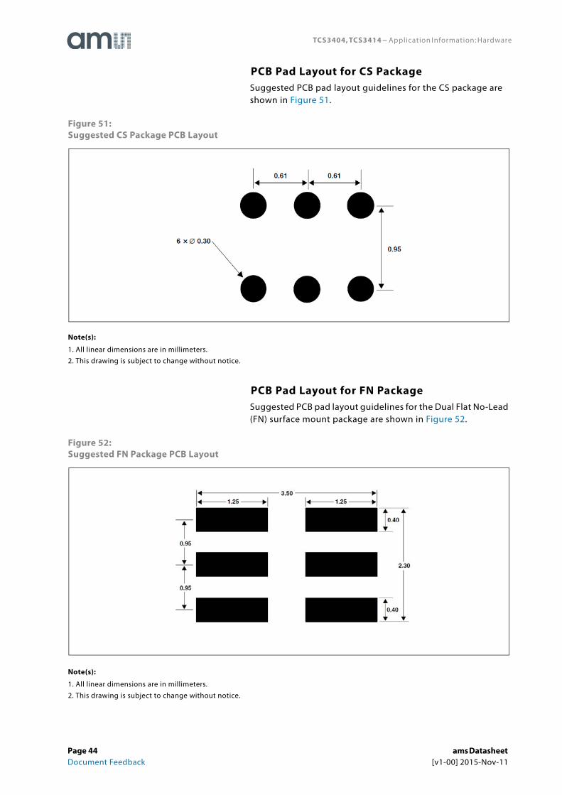
PCB Pad Layout for CS PackageSuggested PCB pad layout guidelines for the CS package are shown in Figure 51.
Figure 51:Suggested CS Package PCB Layout
Note(s):
1. All linear dimensions are in millimeters.
2. This drawing is subject to change without notice.
PCB Pad Layout for FN PackageSuggested PCB pad layout guidelines for the Dual Flat No-Lead (FN) surface mount package are shown in Figure 52.
Figure 52:Suggested FN Package PCB Layout
Note(s):
1. All linear dimensions are in millimeters.
2. This drawing is subject to change without notice.
Page 44 ams Datasheet Document Feedback [v1-00] 2015-Nov-11
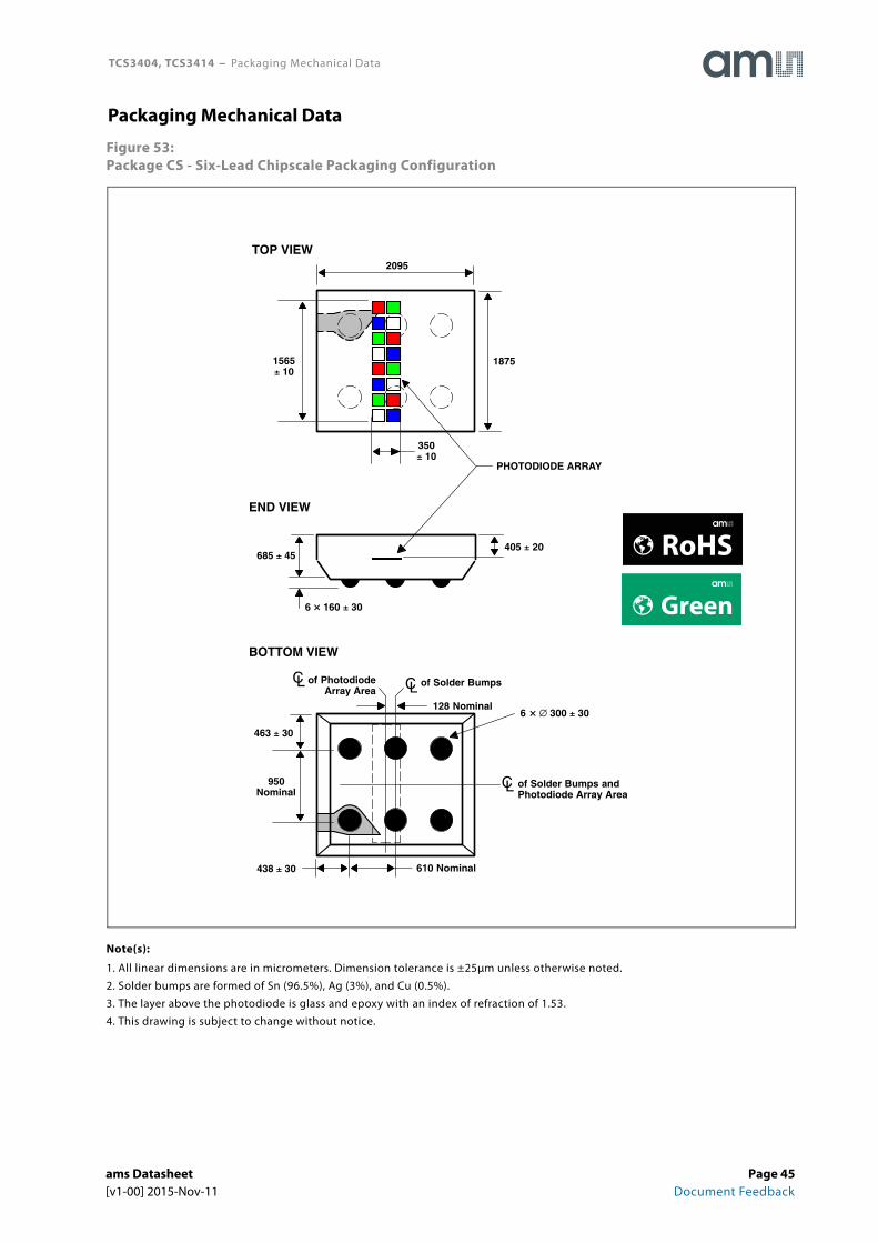
TCS3404, TCS3414 − Packaging Mechanical Data
Figure 53:Package CS - Six-Lead Chipscale Packaging Configuration
Note(s):
1. All linear dimensions are in micrometers. Dimension tolerance is ±25μm unless otherwise noted.
2. Solder bumps are formed of Sn (96.5%), Ag (3%), and Cu (0.5%).
3. The layer above the photodiode is glass and epoxy with an index of refraction of 1.53.
4. This drawing is subject to change without notice.
Packaging Mechanical Data
950Nominal
350� 10
1565� 10
2095
463 � 30
610 Nominal438 � 30
TOP VIEW
BOTTOM VIEW
END VIEW
6 � � 300 � 30
PHOTODIODE ARRAY
1875
128 Nominal
CL of Solder Bumps andPhotodiode Array Area
6 � 160 � 30
405 � 20685 � 45
CL of Solder BumpsCL of PhotodiodeArray Area
Green
RoHS
ams Datasheet Page 45[v1-00] 2015-Nov-11 Document Feedback
TCS3404, TCS3414 − Packaging Mechanical Data
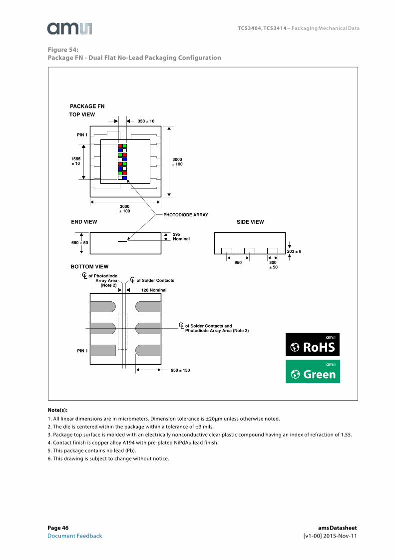
Figure 54:Package FN - Dual Flat No-Lead Packaging Configuration
Note(s):
1. All linear dimensions are in micrometers. Dimension tolerance is ±20μm unless otherwise noted.
2. The die is centered within the package within a tolerance of ±3 mils.
3. Package top surface is molded with an electrically nonconductive clear plastic compound having an index of refraction of 1.55.
4. Contact finish is copper alloy A194 with pre-plated NiPdAu lead finish.
5. This package contains no lead (Pb).
6. This drawing is subject to change without notice.
PACKAGE FN Dual Flat No-Lead
203 � 8
6 GND
5 Vdd
4 INT
SCL 1
SYNC 2
SDA 3
TOP VIEW
SIDE VIEW
BOTTOM VIEW300� 50
950
3000� 100
3000� 100
PIN 1
PIN 1
END VIEW
650 � 50
PIN OUTTOPVIEW
950 � 150
PHOTODIODE ARRAY
295Nominal
350 � 10
1565� 10
128 Nominal
CL of Solder ContactsCL of Photodiode
Array Area(Note )
CL of Solder Contacts andPhotodiode Array Area (Note )
Green
RoHS
Page 46 ams Datasheet Document Feedback [v1-00] 2015-Nov-11
TCS3404, TCS3414 − Packaging Mechanical Data
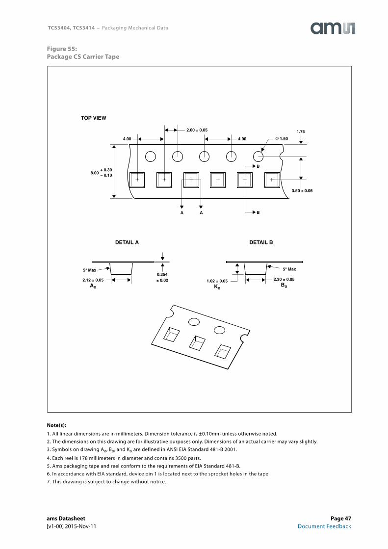
Figure 55:Package CS Carrier Tape
Note(s):
1. All linear dimensions are in millimeters. Dimension tolerance is ±0.10mm unless otherwise noted.
2. The dimensions on this drawing are for illustrative purposes only. Dimensions of an actual carrier may vary slightly.
3. Symbols on drawing Ao, Bo, and Ko are defined in ANSI EIA Standard 481-B 2001.
4. Each reel is 178 millimeters in diameter and contains 3500 parts.
5. Ams packaging tape and reel conform to the requirements of EIA Standard 481-B.
6. In accordance with EIA standard, device pin 1 is located next to the sprocket holes in the tape
7. This drawing is subject to change without notice.
TOP VIEW
DETAIL A
2.12 � 0.05Ao
0.254� 0.02
5� Max
4.00
8.00
3.50 � 0.05
� 1.504.00
2.00 � 0.05
+ 0.30− 0.10
1.75
B
BA A
DETAIL B
2.30 � 0.05Bo
5� Max
1.02 � 0.05Ko
ams Datasheet Page 47[v1-00] 2015-Nov-11 Document Feedback
TCS3404, TCS3414 − Packaging Mechanical Data
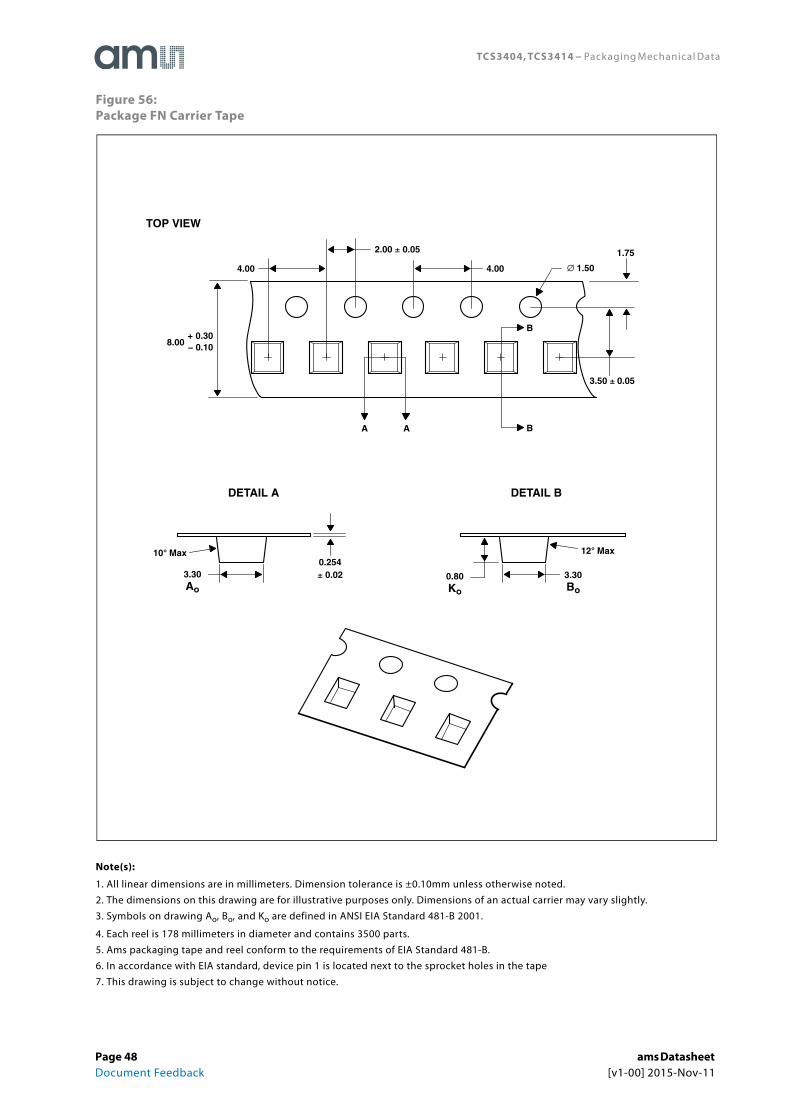
Figure 56:Package FN Carrier Tape
Note(s):
1. All linear dimensions are in millimeters. Dimension tolerance is ±0.10mm unless otherwise noted.
2. The dimensions on this drawing are for illustrative purposes only. Dimensions of an actual carrier may vary slightly.
3. Symbols on drawing Ao, Bo, and Ko are defined in ANSI EIA Standard 481-B 2001.
4. Each reel is 178 millimeters in diameter and contains 3500 parts.
5. Ams packaging tape and reel conform to the requirements of EIA Standard 481-B.
6. In accordance with EIA standard, device pin 1 is located next to the sprocket holes in the tape
7. This drawing is subject to change without notice.
TOP VIEW
DETAIL A
3.30Ao
0.254� 0.02
10� Max
4.00
8.00
3.50 � 0.05
� 1.504.00
2.00 � 0.05
+ 0.30− 0.10
1.75
B
BA A
DETAIL B
3.30Bo
12� Max
0.80Ko
Page 48 ams Datasheet Document Feedback [v1-00] 2015-Nov-11
TCS3404, TCS3414 − Manufacturing Information
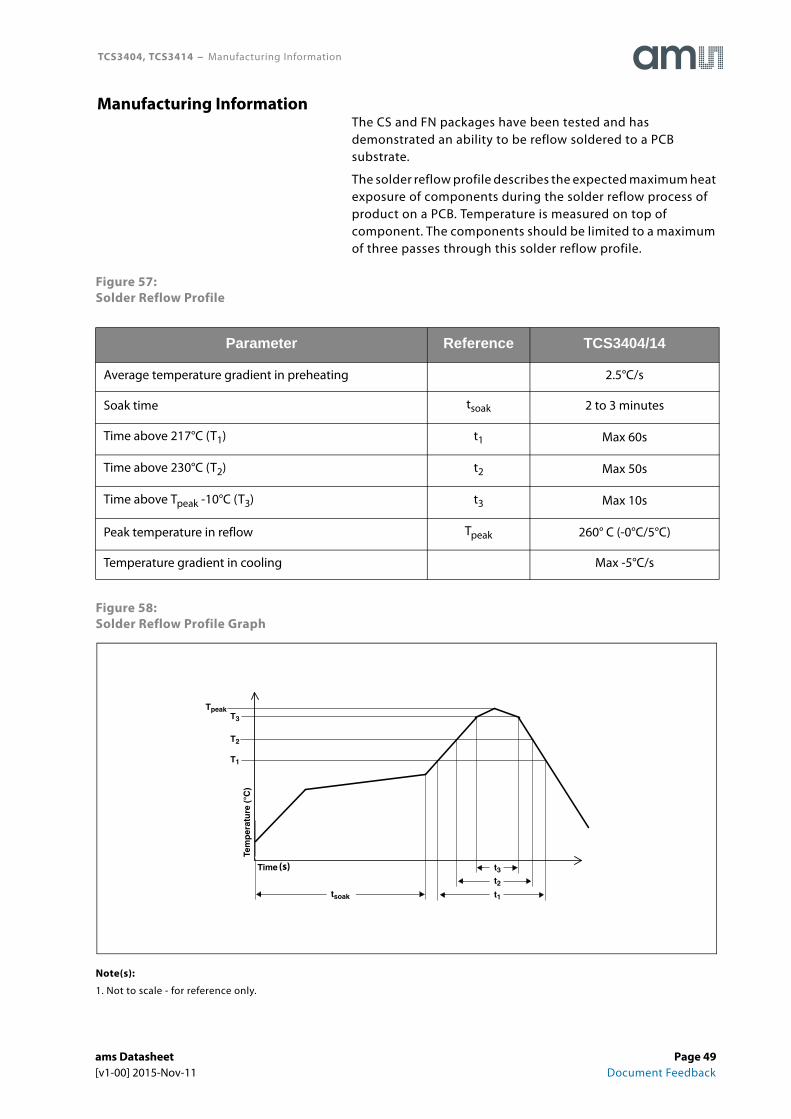
The CS and FN packages have been tested and has demonstrated an ability to be reflow soldered to a PCB substrate.
The solder reflow profile describes the expected maximum heat exposure of components during the solder reflow process of product on a PCB. Temperature is measured on top of component. The components should be limited to a maximum of three passes through this solder reflow profile.
Figure 57:Solder Reflow Profile
Figure 58:Solder Reflow Profile Graph
Note(s):
1. Not to scale - for reference only.
Parameter Reference TCS3404/14
Average temperature gradient in preheating 2.5°C/s
Soak time tsoak 2 to 3 minutes
Time above 217°C (T1) t1 Max 60s
Time above 230°C (T2) t2 Max 50s
Time above Tpeak -10°C (T3) t3 Max 10s
Peak temperature in reflow Tpeak 260° C (-0°C/5°C)
Temperature gradient in cooling Max -5°C/s
Manufacturing Information
t3t2t1tsoak
T3
T2
T1
TpeakNot to scale — for reference only
Time (sec)
Tem
per
atu
re (�C
)
(s)
ams Datasheet Page 49[v1-00] 2015-Nov-11 Document Feedback
TCS3404, TCS3414 − Manufacturing Information
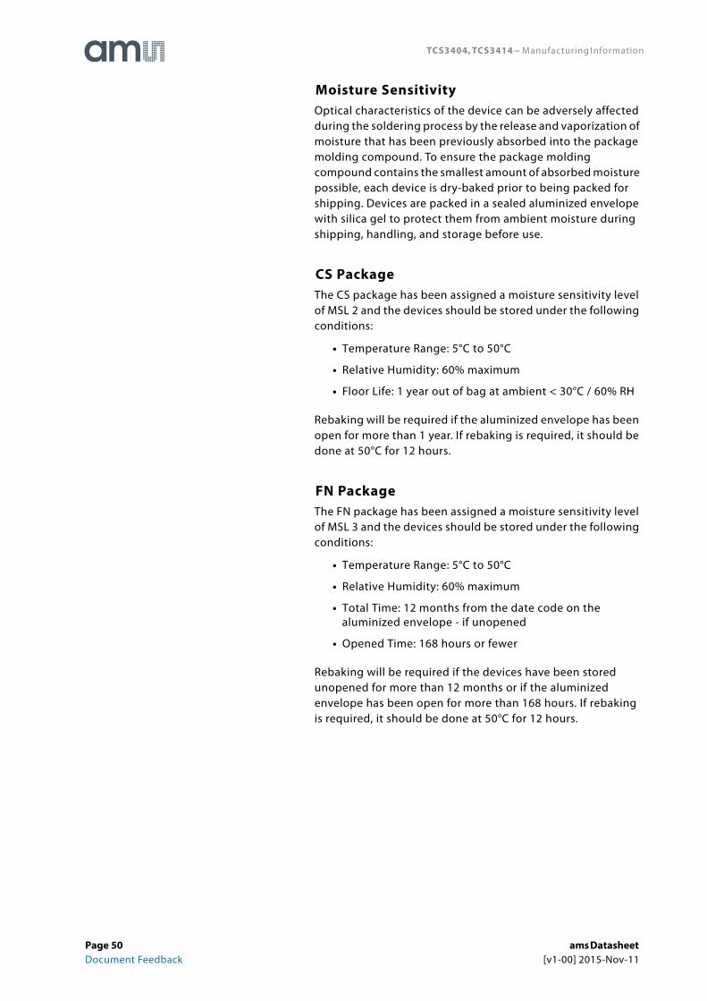
Moisture SensitivityOptical characteristics of the device can be adversely affected during the soldering process by the release and vaporization of moisture that has been previously absorbed into the package molding compound. To ensure the package molding compound contains the smallest amount of absorbed moisture possible, each device is dry-baked prior to being packed for shipping. Devices are packed in a sealed aluminized envelope with silica gel to protect them from ambient moisture during shipping, handling, and storage before use.
CS PackageThe CS package has been assigned a moisture sensitivity level of MSL 2 and the devices should be stored under the following conditions:
• Temperature Range: 5°C to 50°C
• Relative Humidity: 60% maximum
• Floor Life: 1 year out of bag at ambient < 30°C / 60% RH
Rebaking will be required if the aluminized envelope has been open for more than 1 year. If rebaking is required, it should be done at 50°C for 12 hours.
FN PackageThe FN package has been assigned a moisture sensitivity level of MSL 3 and the devices should be stored under the following conditions:
• Temperature Range: 5°C to 50°C
• Relative Humidity: 60% maximum
• Total Time: 12 months from the date code on the aluminized envelope - if unopened
• Opened Time: 168 hours or fewer
Rebaking will be required if the devices have been stored unopened for more than 12 months or if the aluminized envelope has been open for more than 168 hours. If rebaking is required, it should be done at 50°C for 12 hours.
Page 50 ams Datasheet Document Feedback [v1-00] 2015-Nov-11
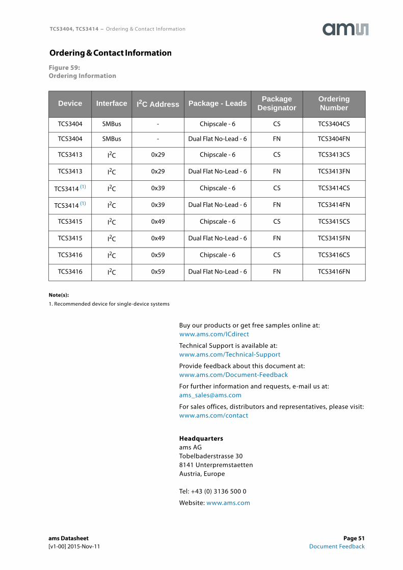
TCS3404, TCS3414 − Ordering & Contact Information
Figure 59:Ordering Information
Note(s):
1. Recommended device for single-device systems
Buy our products or get free samples online at:www.ams.com/ICdirect
Technical Support is available at:www.ams.com/Technical-Support
Provide feedback about this document at:www.ams.com/Document-Feedback
For further information and requests, e-mail us at:[email protected]
For sales offices, distributors and representatives, please visit: www.ams.com/contact
Headquartersams AGTobelbaderstrasse 308141 UnterpremstaettenAustria, Europe
Tel: +43 (0) 3136 500 0
Website: www.ams.com
Device Interface I2C Address Package - LeadsPackage
DesignatorOrdering Number
TCS3404 SMBus - Chipscale - 6 CS TCS3404CS
TCS3404 SMBus - Dual Flat No-Lead - 6 FN TCS3404FN
TCS3413 I2C 0x29 Chipscale - 6 CS TCS3413CS
TCS3413 I2C 0x29 Dual Flat No-Lead - 6 FN TCS3413FN
TCS3414 (1) I2C 0x39 Chipscale - 6 CS TCS3414CS
TCS3414 (1) I2C 0x39 Dual Flat No-Lead - 6 FN TCS3414FN
TCS3415 I2C 0x49 Chipscale - 6 CS TCS3415CS
TCS3415 I2C 0x49 Dual Flat No-Lead - 6 FN TCS3415FN
TCS3416 I2C 0x59 Chipscale - 6 CS TCS3416CS
TCS3416 I2C 0x59 Dual Flat No-Lead - 6 FN TCS3416FN
Ordering & Contact Information
ams Datasheet Page 51[v1-00] 2015-Nov-11 Document Feedback

TCS3404, TCS3414 − RoHS Compliant & ams Green Statement
RoHS: The term RoHS compliant means that ams AG products fully comply with current RoHS directives. Our semiconductor products do not contain any chemicals for all 6 substance categories, including the requirement that lead not exceed 0.1% by weight in homogeneous materials. Where designed to be soldered at high temperatures, RoHS compliant products are suitable for use in specified lead-free processes.
ams Green (RoHS compliant and no Sb/Br): ams Green defines that in addition to RoHS compliance, our products are free of Bromine (Br) and Antimony (Sb) based flame retardants (Br or Sb do not exceed 0.1% by weight in homogeneous material).
Important Information: The information provided in this statement represents ams AG knowledge and belief as of the date that it is provided. ams AG bases its knowledge and belief on information provided by third parties, and makes no representation or warranty as to the accuracy of such information. Efforts are underway to better integrate information from third parties. ams AG has taken and continues to take reasonable steps to provide representative and accurate information but may not have conducted destructive testing or chemical analysis on incoming materials and chemicals. ams AG and ams AG suppliers consider certain information to be proprietary, and thus CAS numbers and other limited information may not be available for release.
RoHS Compliant & ams Green Statement
Page 52 ams Datasheet Document Feedback [v1-00] 2015-Nov-11

TCS3404, TCS3414 − Copyrights & Disclaimer
Copyright ams AG, Tobelbader Strasse 30, 8141 Unterpremstaetten, Austria-Europe. Trademarks Registered. All rights reserved. The material herein may not be reproduced, adapted, merged, translated, stored, or used without the prior written consent of the copyright owner.
Devices sold by ams AG are covered by the warranty and patent indemnification provisions appearing in its General Terms of Trade. ams AG makes no warranty, express, statutory, implied, or by description regarding the information set forth herein. ams AG reserves the right to change specifications and prices at any time and without notice. Therefore, prior to designing this product into a system, it is necessary to check with ams AG for current information. This product is intended for use in commercial applications. Applications requiring extended temperature range, unusual environmental requirements, or high reliability applications, such as military, medical life-support or life-sustaining equipment are specifically not recommended without additional processing by ams AG for each application. This product is provided by ams AG “AS IS” and any express or implied warranties, including, but not limited to the implied warranties of merchantability and fitness for a particular purpose are disclaimed.
ams AG shall not be liable to recipient or any third party for any damages, including but not limited to personal injury, property damage, loss of profits, loss of use, interruption of business or indirect, special, incidental or consequential damages, of any kind, in connection with or arising out of the furnishing, performance or use of the technical data herein. No obligation or liability to recipient or any third party shall arise or flow out of ams AG rendering of technical or other services.
Copyrights & Disclaimer
ams Datasheet Page 53[v1-00] 2015-Nov-11 Document Feedback
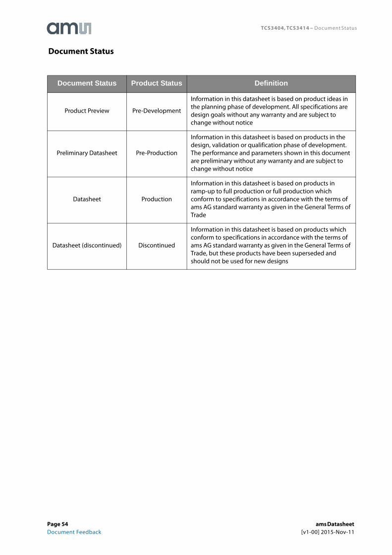
TCS3404, TCS3414 − Document Status
Document Status Product Status Definition
Product Preview Pre-Development
Information in this datasheet is based on product ideas in the planning phase of development. All specifications are design goals without any warranty and are subject to change without notice
Preliminary Datasheet Pre-Production
Information in this datasheet is based on products in the design, validation or qualification phase of development. The performance and parameters shown in this document are preliminary without any warranty and are subject to change without notice
Datasheet Production
Information in this datasheet is based on products in ramp-up to full production or full production which conform to specifications in accordance with the terms of ams AG standard warranty as given in the General Terms of Trade
Datasheet (discontinued) Discontinued
Information in this datasheet is based on products which conform to specifications in accordance with the terms of ams AG standard warranty as given in the General Terms of Trade, but these products have been superseded and should not be used for new designs
Document Status
Page 54 ams Datasheet Document Feedback [v1-00] 2015-Nov-11
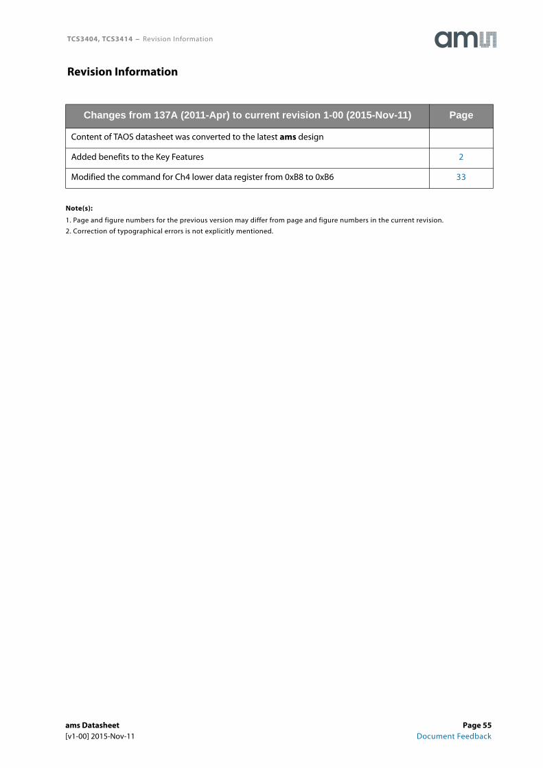
TCS3404, TCS3414 − Revision Information
Note(s):
1. Page and figure numbers for the previous version may differ from page and figure numbers in the current revision.
2. Correction of typographical errors is not explicitly mentioned.
Changes from 137A (2011-Apr) to current revision 1-00 (2015-Nov-11) Page
Content of TAOS datasheet was converted to the latest ams design
Added benefits to the Key Features 2
Modified the command for Ch4 lower data register from 0xB8 to 0xB6 33
Revision Information
ams Datasheet Page 55[v1-00] 2015-Nov-11 Document Feedback

TCS3404, TCS3414 − Content Guide
1 General Description2 Key Benefits & Features3 Applications3 End Products and Market Segments3 Block Diagram
4 Pin Assignments5 Absolute Maximum Ratings6 Electrical Characteristics10 Parameter Measurement Information11 Typical Operating Characteristics
15 Principles of Operation15 Analog-to-Digital Converter15 Digital Interface16 Interrupt16 SMBus and I2C Protocols21 Register Set22 Command Register23 Control Register (00h)24 Timing Register (01h)26 Interrupt Control Register (02h)28 Interrupt Source Register (03h)28 ID Register (04h)29 Gain Register (07h)31 Interrupt Threshold Register (08h - 0Bh)32 ADC Channel Data Registers (10h - 17h)
33 Application Information: Software33 Basic Operation35 Configuring the Timing Register36 Synchronization41 Interrupts
43 Application Information: Hardware43 Power Supply Decoupling and Application Hardware
Circuit44 PCB Pad Layout for CS Package44 PCB Pad Layout for FN Package
45 Packaging Mechanical Data
49 Manufacturing Information50 Moisture Sensitivity50 CS Package50 FN Package
51 Ordering & Contact Information52 RoHS Compliant & ams Green Statement53 Copyrights & Disclaimer54 Document Status55 Revision Information
Content Guide
Page 56 ams Datasheet Document Feedback [v1-00] 2015-Nov-11


![A comparison of single-cell trajectory inference methods ... · BGP 01/08/2017 Bifurcation TBD TBD TBD Noj [57] scanpy 09/08/2017 Bifurcation TBD TBD TBD Noj [58] B-RGPs 01/09/2017](https://img.pdfslide.net/doc/110x75/5faef63686c74474a31efbdd/a-comparison-of-single-cell-trajectory-inference-methods-bgp-01082017-bifurcation.jpg)