Embed Size (px)
Citation preview
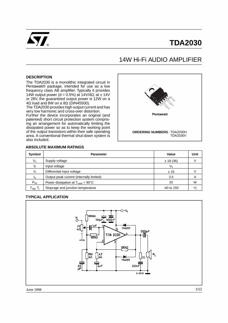
® TDA2030
14W Hi-Fi AUDIO AMPLIFIER
DESCRIPTIONThe TDA2030 is a monolithic integrated circuit inPentawatt® package, intended for use as a lowfrequency class AB amplifier. Typically it provides14W output power (d = 0.5%) at 14V/4Ω; at ± 14Vor 28V, the guaranteed output power is 12W on a4Ω load and 8W on a 8Ω (DIN45500).The TDA2030 provides high output current and hasvery low harmonic and cross-over distortion.Further the device incorporates an original (andpatented) short circuit protection system compris-ing an arrangement for automatically limiting thedissipated power so as to keep the working pointof the output transistors within their safe operatingarea. A conventional thermal shut-down system isalso included.
June 1998
Symbol Parameter Value Unit
Vs Supply voltage ± 18 (36) V
Vi Input voltage Vs
Vi Differential input voltage ± 15 V
Io Output peak current (internally limited) 3.5 A
Ptot Power dissipation at Tcase = 90°C 20 W
Tstg, Tj Stoprage and junction temperature -40 to 150 °C
ABSOLUTE MAXIMUM RATINGS
TYPICAL APPLICATION
Pentawatt
ORDERING NUMBERS : TDA2030H TDA2030V
1/12
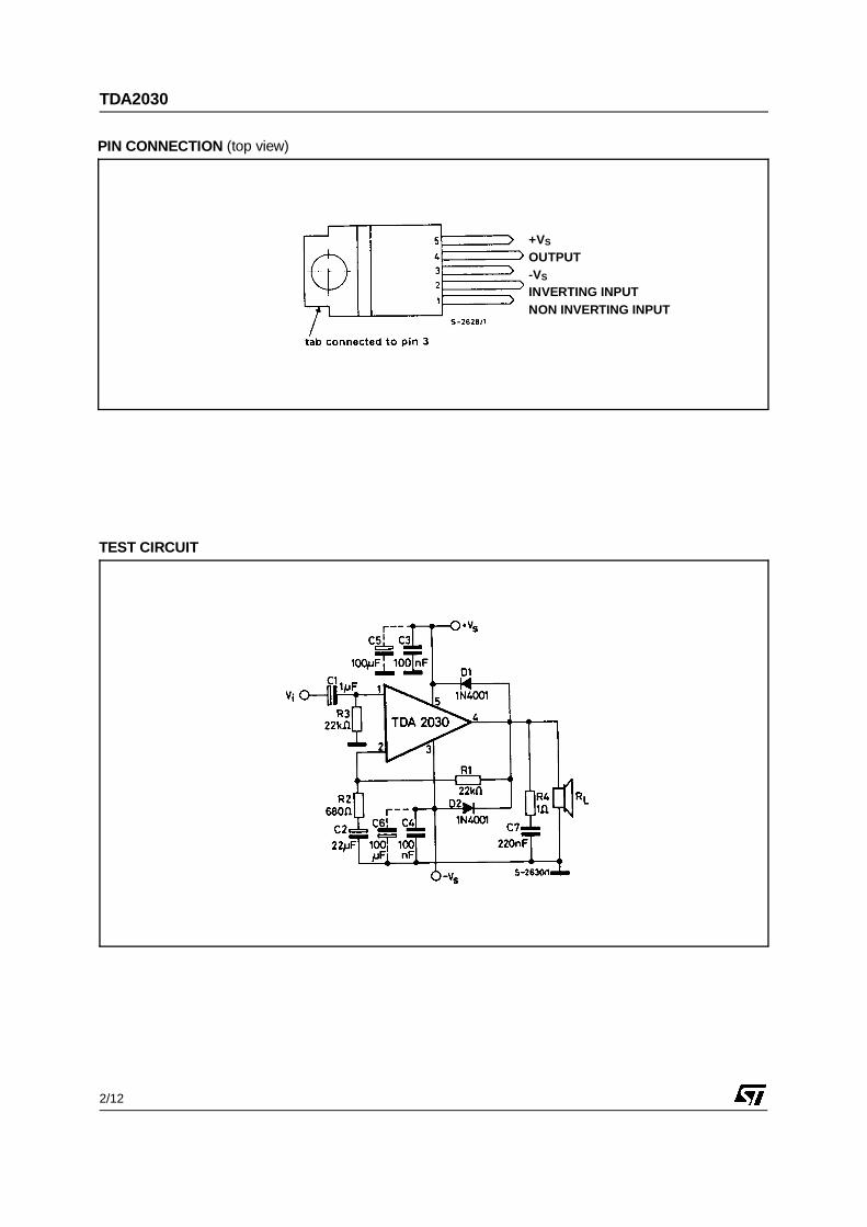
PIN CONNECTION (top view)
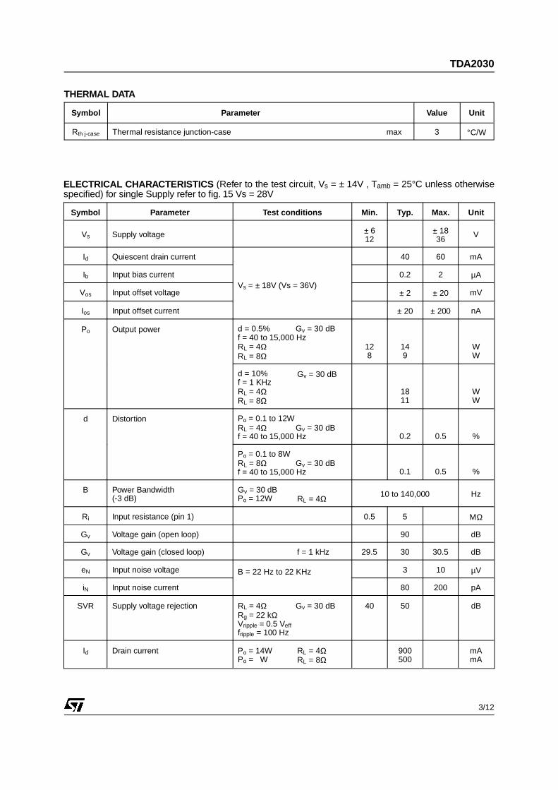
TEST CIRCUIT
+VS
OUTPUT-VS
INVERTING INPUTNON INVERTING INPUT
TDA2030
2/12
Symbol Parameter Test conditions Min. Typ. Max. Unit
Vs Supply voltage ± 612
± 1836
V
Id Quiescent drain current
Vs = ± 18V (Vs = 36V)
40 60 mA
Ib Input bias current 0.2 2 µA
Vos Input offset voltage ± 2 ± 20 mV
Ios Input offset current ± 20 ± 200 nA
Po Output power d = 0.5% Gv = 30 dBf = 40 to 15,000 HzRL = 4ΩRL = 8Ω
128
149
WW
d = 10%f = 1 KHzRL = 4ΩRL = 8Ω
Gv = 30 dB
1811
WW
d Distortion Po = 0.1 to 12W RL = 4Ω Gv = 30 dBf = 40 to 15,000 Hz
0.2 0.5 %
Po = 0.1 to 8WRL = 8Ω Gv = 30 dBf = 40 to 15,000 Hz
0.1 0.5 %
B Power Bandwidth(-3 dB)
Gv = 30 dBPo = 12W RL = 4Ω 10 to 140,000 Hz
Ri Input resistance (pin 1) 0.5 5 MΩ
Gv Voltage gain (open loop) 90 dB
Gv Voltage gain (closed loop) f = 1 kHz 29.5 30 30.5 dB
eN Input noise voltage B = 22 Hz to 22 KHz 3 10 µV
iN Input noise current 80 200 pA
SVR Supply voltage rejection RL = 4Ω Gv = 30 dBRg = 22 kΩVripple = 0.5 Vefffripple = 100 Hz
40 50
dB
Id Drain current Po = 14WPo = W
RL = 4ΩRL = 8Ω 900
500 mAmA
ELECTRICAL CHARACTERISTICS (Refer to the test circuit, Vs = ± 14V , Tamb = 25°C unless otherwisespecified) for single Supply refer to fig. 15 Vs = 28V
Symbol Parameter Value Unit
Rth j-case Thermal resistance junction-case max 3 °C/W
THERMAL DATA
TDA2030
3/12
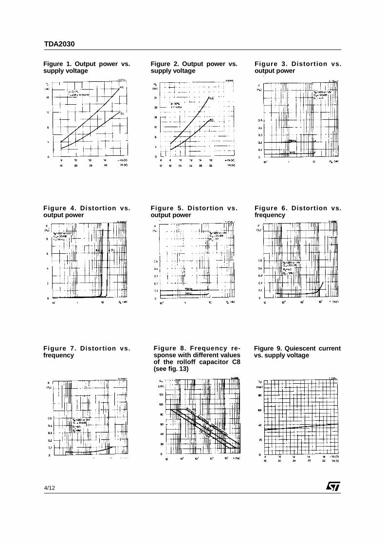
Figure 1. Output power vs.supply voltage
Figure 2. Output power vs.supply voltage
Figure 3. Distort ion vs.output power
Figure 4. Distort ion vs.output power
Figure 5. Distor tion vs.output power
Figure 6. Distort ion vs.frequency
Figure 7. Distor tion vs.frequency
Figure 8. Frequency re-sponse with different valuesof the rolloff capacitor C8(see fig. 13)
Figure 9. Quiescent currentvs. supply voltage
TDA2030
4/12
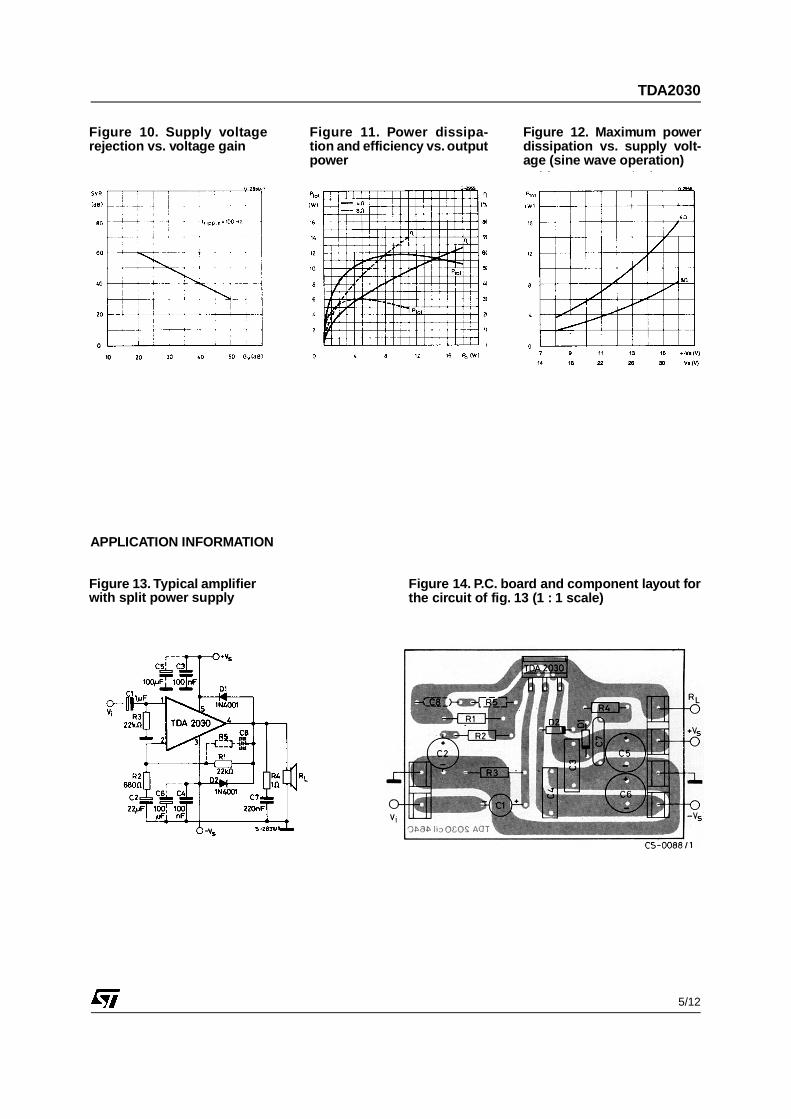
Figure 10. Supply voltagerejection vs. voltage gain
Figure 11. Power dissipa-tion and efficiency vs. outputpower
Figure 12. Maximum powerdissipation vs. supply volt-age (sine wave operation)
APPLICATION INFORMATION
Figure 13. Typical amplifierwith split power supply
Figure 14. P.C. board and component layout forthe circuit of fig. 13 (1 : 1 scale)
TDA2030
5/12
APPLICATION INFORMATION (continued)
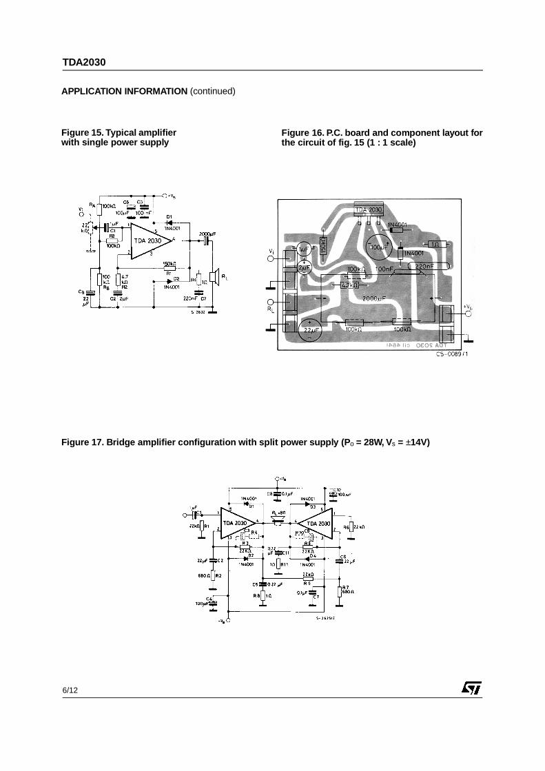
Figure 15. Typical amplifierwith single power supply
Figure 16. P.C. board and component layout forthe circuit of fig. 15 (1 : 1 scale)
Figure 17. Bridge amplifier configuration with split power supply (P o = 28W, Vs = ±14V)
TDA2030
6/12
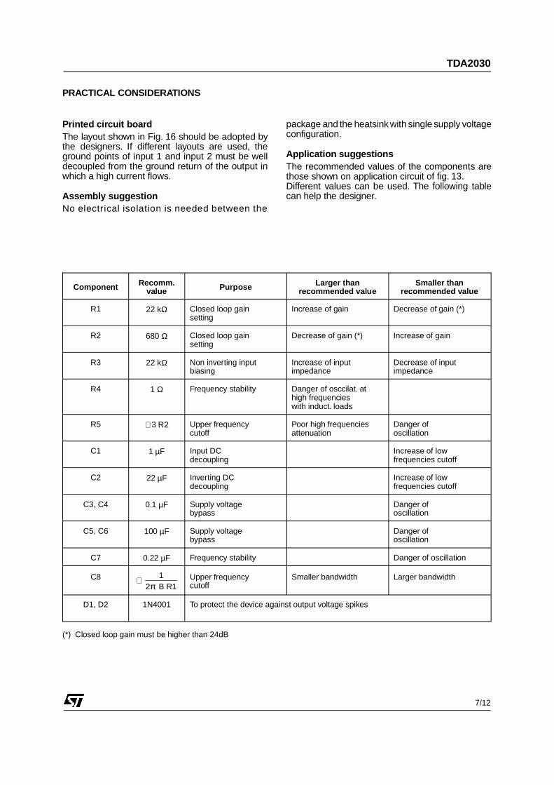
PRACTICAL CONSIDERATIONS
Printed circuit boardThe layout shown in Fig. 16 should be adopted bythe designers. If different layouts are used, theground points of input 1 and input 2 must be welldecoupled from the ground return of the output inwhich a high current flows.
Assembly suggestionNo electrical isolation is needed between the
package and the heatsink with single supply voltageconfiguration.
Application suggestionsThe recommended values of the components arethose shown on application circuit of fig. 13.Different values can be used. The following tablecan help the designer.
Component Recomm.value Purpose Larger than
recommended valueSmaller than
recommended value
R1 22 kΩ Closed loop gainsetting
Increase of gain Decrease of gain (*)
R2 680 Ω Closed loop gainsetting
Decrease of gain (*) Increase of gain
R3 22 kΩ Non inverting inputbiasing
Increase of inputimpedance
Decrease of inputimpedance
R4 1 Ω Frequency stability Danger of osccilat. athigh frequencieswith induct. loads
R5 ≅ 3 R2 Upper frequencycutoff
Poor high frequenciesattenuation
Danger ofoscillation
C1 1 µF Input DCdecoupling Increase of low
frequencies cutoff
C2 22 µF Inverting DCdecoupling Increase of low
frequencies cutoff
C3, C4 0.1 µF Supply voltagebypass Danger of
oscillation
C5, C6 100 µF Supply voltagebypass Danger of
oscillation
C7 0.22 µF Frequency stability Danger of oscillation
C8 ≅ 1
2π B R1Upper frequencycutoff
Smaller bandwidth Larger bandwidth
D1, D2 1N4001 To protect the device against output voltage spikes
(*) Closed loop gain must be higher than 24dB
TDA2030
7/12
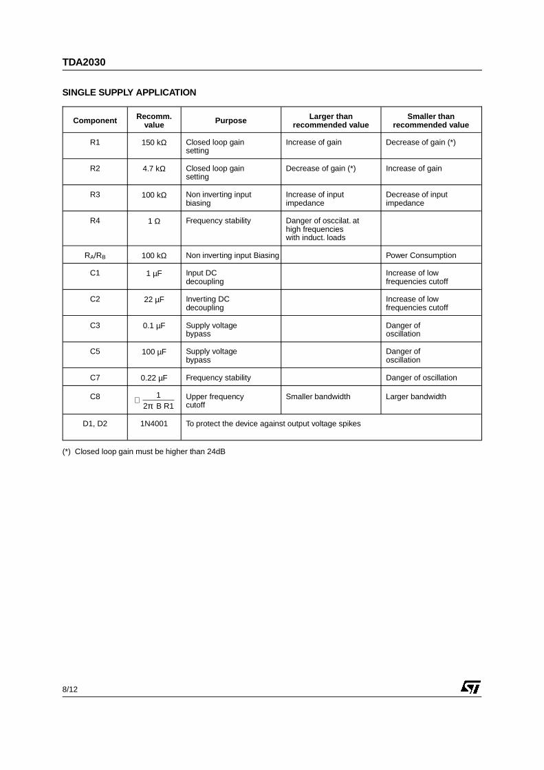
SINGLE SUPPLY APPLICATION
Component Recomm.value Purpose Larger than
recommended valueSmaller than
recommended value
R1 150 kΩ Closed loop gainsetting
Increase of gain Decrease of gain (*)
R2 4.7 kΩ Closed loop gainsetting
Decrease of gain (*) Increase of gain
R3 100 kΩ Non inverting inputbiasing
Increase of inputimpedance
Decrease of inputimpedance
R4 1 Ω Frequency stability Danger of osccilat. athigh frequencieswith induct. loads
RA/RB 100 kΩ Non inverting input Biasing Power Consumption
C1 1 µF Input DCdecoupling Increase of low
frequencies cutoff
C2 22 µF Inverting DCdecoupling Increase of low
frequencies cutoff
C3 0.1 µF Supply voltagebypass Danger of
oscillation
C5 100 µF Supply voltagebypass Danger of
oscillation
C7 0.22 µF Frequency stability Danger of oscillation
C8 ≅ 1
2π B R1Upper frequencycutoff
Smaller bandwidth Larger bandwidth
D1, D2 1N4001 To protect the device against output voltage spikes
(*) Closed loop gain must be higher than 24dB
TDA2030
8/12
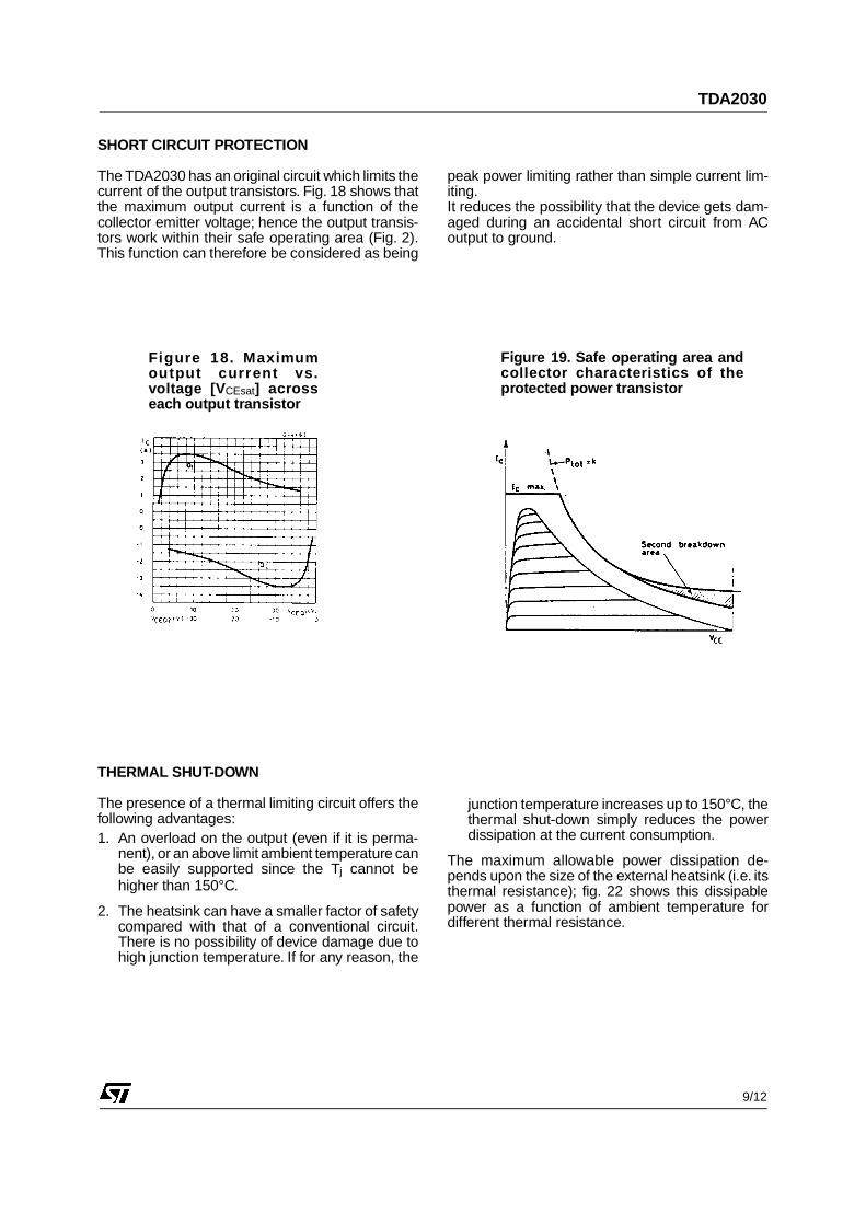
SHORT CIRCUIT PROTECTION
The TDA2030 has an original circuit which limits thecurrent of the output transistors. Fig. 18 shows thatthe maximum output current is a function of thecollector emitter voltage; hence the output transis-tors work within their safe operating area (Fig. 2).This function can therefore be considered as being
peak power limiting rather than simple current lim-iting.It reduces the possibility that the device gets dam-aged during an accidental short circuit from ACoutput to ground.
Figure 18. Maximumoutput current vs.voltage [V CEsat] acrosseach output transistor
Figure 19. Safe operating area andcollector characteristics of theprotected power transistor
THERMAL SHUT-DOWN
The presence of a thermal limiting circuit offers thefollowing advantages:1. An overload on the output (even if it is perma-
nent), or an above limit ambient temperature canbe easily supported since the Tj cannot behigher than 150°C.
2. The heatsink can have a smaller factor of safetycompared with that of a conventional circuit.There is no possibility of device damage due tohigh junction temperature. If for any reason, the
junction temperature increases up to 150°C, thethermal shut-down simply reduces the powerdissipation at the current consumption.
The maximum allowable power dissipation de-pends upon the size of the external heatsink (i.e. itsthermal resistance); fig. 22 shows this dissipablepower as a function of ambient temperature fordifferent thermal resistance.
TDA2030
9/12
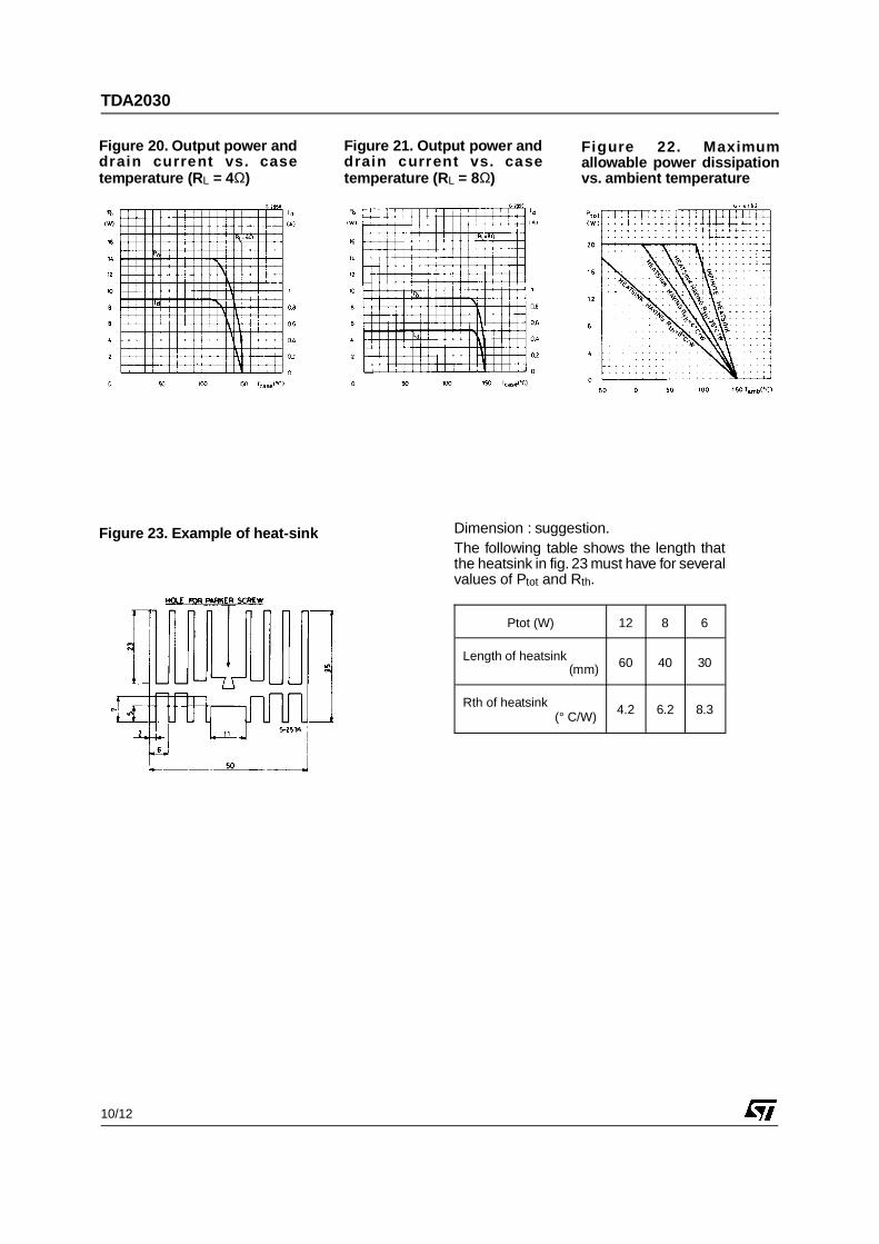
Figure 20. Output power anddrain current vs. casetemperature (R L = 4Ω)
Figure 21. Output power anddrain current vs. casetemperature (R L = 8Ω)
Figure 22. Maximumallowable power dissipationvs. ambient temperature
Figure 23. Example of heat-sink Dimension : suggestion.The following table shows the length thatthe heatsink in fig. 23 must have for severalvalues of Ptot and Rth.
Ptot (W) 12 8 6
Length of heatsink (mm) 60 40 30
Rth of heatsink (° C/W)
4.2 6.2 8.3
TDA2030
10/12
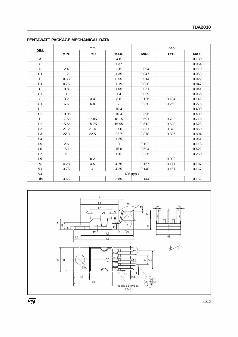
DIM.mm inch
MIN. TYP. MAX. MIN. TYP. MAX.A 4.8 0.189C 1.37 0.054D 2.4 2.8 0.094 0.110
D1 1.2 1.35 0.047 0.053E 0.35 0.55 0.014 0.022
E1 0.76 1.19 0.030 0.047F 0.8 1.05 0.031 0.041
F1 1 1.4 0.039 0.055G 3.2 3.4 3.6 0.126 0.134 0.142
G1 6.6 6.8 7 0.260 0.268 0.276H2 10.4 0.409H3 10.05 10.4 0.396 0.409L 17.55 17.85 18.15 0.691 0.703 0.715
L1 15.55 15.75 15.95 0.612 0.620 0.628L2 21.2 21.4 21.6 0.831 0.843 0.850L3 22.3 22.5 22.7 0.878 0.886 0.894L4 1.29 0.051L5 2.6 3 0.102 0.118L6 15.1 15.8 0.594 0.622L7 6 6.6 0.236 0.260L9 0.2 0.008M 4.23 4.5 4.75 0.167 0.177 0.187
M1 3.75 4 4.25 0.148 0.157 0.167V4 40° (typ.)Dia 3.65 3.85 0.144 0.152
PENTAWATT PACKAGE MECHANICAL DATA
L
L1
A
C
L5
D1 L2
L3
E
M1
MD
H3
Dia.
L7
L6
F1H2
F
G G1
E1F
E
L9V4
R
R
R
RESIN BETWEENLEADS
H1
V3
H2
L8V VV1
B
V V
V4
V4
TDA2030
11/12
Information furnished is believed to be accurate and reliable. However, STMicroelectronics assumes no responsibility for the consequences ofuse of such information nor for any infringement of patents or other rights of third parties which may result from its use. No license is grantedby implication or otherwise under any patent or patent rights of STMicroelectronics. Specification mentioned in this publication are subject tochange without notice. This publication supersedes and replaces all information previously supplied. STMicroelectronics products are notauthorized for use as critical components in life support devices or systems without express written approval of STMicroelectronics.
The ST logo is a registered trademark of STMicroelectronics© 1998 STMicroelectronics – Printed in Italy – All Rights Reserved
STMicroelectronics GROUP OF COMPANIESAustralia - Brazil - Canada - China - France - Germany - Italy - Japan - Korea - Malaysia - Malta - Mexico - Morocco - The Netherlands -
Singapore - Spain - Sweden - Switzerland - Taiwan - Thailand - United Kingdom - U.S.A.
TDA2030
12/12

This datasheet has been download from:
www.datasheetcatalog.com
Datasheets for electronics components.