Embed Size (px)
Citation preview

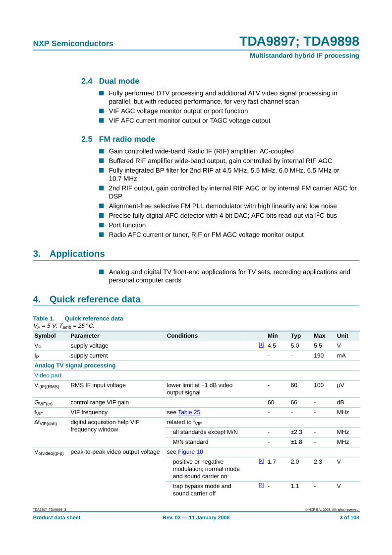
1. General description
The Integrated Circuit (IC) is suitable for Intermediate Frequency (IF) processing includingglobal multistandard Analog TV (ATV), Digital Video Broadcast (DVB) and mono FM radiousing only 1 IC and 1 to 3 fixed Surface Acoustic Waves (SAWs) (application dependent).TDA9898 including L and L-accent standard. TDA9897 without L and L-accent standard.
2. Features
2.1 Generaln 5 V supply voltage
n I2C-bus control over all functions
n Four I2C-bus addresses provided; selection by programmable Module Address (MAD)
n Three I2C-bus voltage level supported; selection via pin BVS
n Separate gain controlled amplifiers with input selector and conversion for incoming IF[analog Vision IF (VIF) or Sound IF (SIF) or Digital TV (DTV)] allows the use ofdifferent filter shapes and bandwidths
n All conventional ATV standards applicable by using DTV bandwidth window[Band-Pass (BP)] filter
n Easy to use default settings for almost every standard provided, selectable via I2C-bus
n Two 4 MHz reference frequency stages; the first one operates as crystal oscillator, thesecond one as external signal input
n Stabilizer circuit for ripple rejection and to achieve constant output signals
n Smallest size, simplest application
n ElectroStatic Discharge (ESD) protection for all pins
2.2 Analog TV processingn Gain controlled wide-band VIF amplifier; AC-coupled
n Multistandard true synchronous demodulation with active carrier regeneration: verylinear demodulation, good intermodulation figures, reduced harmonics and excellentpulse response
n Internal Nyquist slope processing; switch-off able for alternative use of inexpensiveNyquist slope SAW filter with additive video noise improvement
n Gated phase detector for L and L-accent standards
n Fully integrated VIF Voltage-Controlled Oscillator (VCO), alignment-free, frequenciesswitchable for all negative and positive modulated standards via I2C-bus
n VIF Automatic Gain Control (AGC) detector for gain control; operating as a peak syncdetector for negative modulated signals and as a peak white detector for positivemodulated signals
TDA9897; TDA9898Multistandard hybrid IF processingRev. 03 — 11 January 2008 Product data sheet

NXP Semiconductors TDA9897; TDA9898Multistandard hybrid IF processing
n Optimized AGC modes for negative modulation; e.g. very fast reaction time for VIF andSIF
n Precise fully digital Automatic Frequency Control (AFC) detector with 4-bitDigital-to-Analog Converter (DAC); AFC bits can be read-out via I2C-bus
n High precise Tuner AGC (TAGC) TakeOver Point (TOP) for negative modulatedstandards; TOP adjust via I2C-bus
n TAGC TOP for positive standards and Received Signal Strength Indication (RSSI);adjustable via I2C-bus or alternatively by potentiometer
n Fully integrated Sound Carrier (SC) trap for any ATV standard (SC at 4.5 MHz,5.5 MHz, 6.0 MHz and 6.5 MHz)
n SIF AGC for gain controlled SIF amplifier and high-performance single-referenceQuasi Split Sound (QSS) mixer
n Fully integrated sound BP filter supporting any ATV standard
n Optional use of external FM sound BP filter
n AM sound demodulation for L and L-accent standard
n Alignment-free selective FM Phase-Locked Loop (PLL) demodulator with high linearityand low noise; external FM input
n VIF AGC voltage monitor output or port function
n VIF AFC current or tuner, SIF or FM AGC voltage monitor output
n 2nd SIF output, gain controlled by internal SIF AGC or by internal FM carrier AGC forDigital Signal Processor (DSP)
n Fully integrated BP filter for 2nd SIF at 4.5 MHz, 5.5 MHz, 6.0 MHz or 6.5 MHz
2.3 Digital TV processingn Applicable for terrestrial and cable TV reception
n 70 dB variable gain wide-band IF amplifier (AC-coupled)
n Gain control via external control voltage (0 V to 3 V)
n 2 V (p-p) differential low IF (downconverted) output or 1 V (p-p) 1st IF output for directAnalog-to-Digital Converter (ADC) interfacing
n DVB downconversion with integrated selectivity for Low IF (LIF)/Zero IF (ZIF)
n Integrated anti-aliasing tracking low-pass filter
n Fully integrated synthesizer controlled oscillator with excellent phase noiseperformance
n Synthesizer frequencies for a wide range of world wide DVB standards (for IF centerfrequencies of 34.5 MHz, 36 MHz, 44 MHz and 57 MHz)
n All DVB bandwidth ranges supported (including ZIF I/Q)
n TAGC detector for independent tuner gain control loop applications
n TAGC operating as peak detector, fast reaction time due to additional speed-updetector
n Port function
n TAGC voltage monitor output
TDA9897_TDA9898_3 © NXP B.V. 2008. All rights reserved.
Product data sheet Rev. 03 — 11 January 2008 2 of 103
NXP Semiconductors TDA9897; TDA9898Multistandard hybrid IF processing
2.4 Dual moden Fully performed DTV processing and additional ATV video signal processing in
parallel, but with reduced performance, for very fast channel scan
n VIF AGC voltage monitor output or port function
n VIF AFC current monitor output or TAGC voltage output
2.5 FM radio moden Gain controlled wide-band Radio IF (RIF) amplifier; AC-coupled
n Buffered RIF amplifier wide-band output, gain controlled by internal RIF AGC
n Fully integrated BP filter for 2nd RIF at 4.5 MHz, 5.5 MHz, 6.0 MHz, 6.5 MHz or10.7 MHz
n 2nd RIF output, gain controlled by internal RIF AGC or by internal FM carrier AGC forDSP
n Alignment-free selective FM PLL demodulator with high linearity and low noise
n Precise fully digital AFC detector with 4-bit DAC; AFC bits read-out via I2C-bus
n Port function
n Radio AFC current or tuner, RIF or FM AGC voltage monitor output
3. Applications
n Analog and digital TV front-end applications for TV sets, recording applications andpersonal computer cards
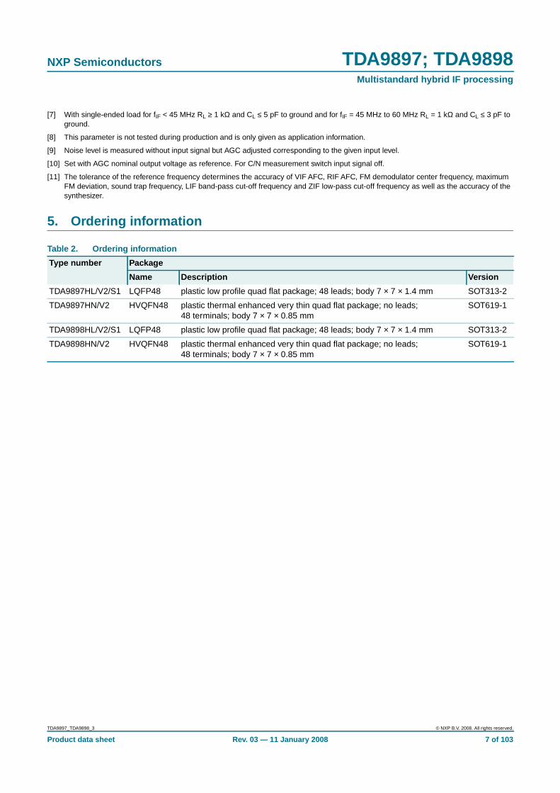
4. Quick reference data
Table 1. Quick reference dataVP = 5 V; Tamb = 25 °C.
Symbol Parameter Conditions Min Typ Max Unit
VP supply voltage [1] 4.5 5.0 5.5 V
IP supply current - - 190 mA
Analog TV signal processing
Video part
Vi(IF)(RMS) RMS IF input voltage lower limit at −1 dB videooutput signal
- 60 100 µV
GVIF(cr) control range VIF gain 60 66 - dB
fVIF VIF frequency see Table 25 - - - MHz
∆fVIF(dah) digital acquisition help VIFfrequency window
related to fVIF
all standards except M/N - ±2.3 - MHz
M/N standard - ±1.8 - MHz
Vo(video)(p-p) peak-to-peak video output voltage see Figure 10
positive or negativemodulation; normal modeand sound carrier on
[2] 1.7 2.0 2.3 V
trap bypass mode andsound carrier off
[3] - 1.1 - V
TDA9897_TDA9898_3 © NXP B.V. 2008. All rights reserved.
Product data sheet Rev. 03 — 11 January 2008 3 of 103

NXP Semiconductors TDA9897; TDA9898Multistandard hybrid IF processing
Gdif differential gain “ITU-T J.63 line 330” [2][4]
B/G standard - - 5 %
L standard - - 7 %
ϕdif differential phase “ITU-T J.63 line 330” [2][4]
B/G standard - 2 4 deg
L standard - 2 4 deg
Bvideo(−3dB) −3 dB video bandwidth trap bypass mode andsound carrier off; AC load:CL < 20 pF, RL > 1 kΩ
[3] 6 8 - MHz
αSC1 first sound carrier attenuation M/N standard;f = fSC1 = 4.5 MHz;see Figure 21
[3] 38 - - dB
B/G standard;f = fSC1 = 5.5 MHz;see Figure 23
[3] 35 - - dB
(S/N)w weighted signal-to-noise ratio normal mode and soundcarrier on; B/G standard;50 % grey video signal;unified weighting filter(“ITU-T J.61”);see Figure 20
[2][5] 53 57 - dB
PSRRCVBS power supply ripple rejection onpin CVBS
normal mode and soundcarrier on; fripple = 70 Hz;video signal; grey level;positive and negativemodulation; see Figure 11
[2] 14 20 - dB
∆IAFC/∆fVIF change of AFC current with VIFfrequency
AFC TV mode [6] 0.85 1.05 1.25 µA/kHz
Audio part
Vo(AF)(RMS) RMS AF output voltage FM: QSS mode;27 kHz FM deviation;50 µs de-emphasis
430 540 650 mV
AM: 54 % modulation 400 500 600 mV
THD total harmonic distortion FM: 50 µs de-emphasis;FM deviation: for TV mode27 kHz and for radio mode22.5 kHz
- 0.15 0.50 %
AM: 54 % modulation;BP on; see Figure 33
- 0.5 1.0 %
f−3dB(AF) AF cut-off frequency W3[2] = 0; W3[4] = 0;without de-emphasis;FM windowwidth = 237.5 kHz
80 100 - kHz
Table 1. Quick reference data …continuedVP = 5 V; Tamb = 25 °C.
Symbol Parameter Conditions Min Typ Max Unit
TDA9897_TDA9898_3 © NXP B.V. 2008. All rights reserved.
Product data sheet Rev. 03 — 11 January 2008 4 of 103

NXP Semiconductors TDA9897; TDA9898Multistandard hybrid IF processing
(S/N)w(AF) AF weighted signal-to-noise ratio “ITU-R BS.468-4”
FM: 27 kHz FM deviation;50 µs de-emphasis; visioncarrier unmodulated;FM PLL only
48 56 - dB
AM: BP off 44 50 - dB
PSRR power supply ripple rejection fripple = 70 Hz; see Figure 11 14 20 - dB
Vo(RMS) RMS output voltage IF intercarrier single-endedto GND; SC1 on; SC2 off
90 140 180 mV
IF intercarrier single-endedto GND; L standard;without modulation; BP on;W7[5] = 0
45 70 90 mV
FM sound part
Vi(FM)(RMS) RMS FM input voltage gain controlled operation;W1[1:0] = 10 orW1[1:0] = 11 orW1[1:0] = 01; see Figure 15
2 - 300 mV
∆IAFC/∆fRIF change of AFC current with RIFfrequency
AFC radio mode [6] 0.85 1.05 1.25 µA/kHz
αAM AM suppression referenced to 27 kHzFM deviation;50 µs de-emphasis;AM: f = 1 kHz; m = 54 %
35 46 - dB
Digital TV signal processing
Digital direct IF
Vo(dif)(p-p) peak-to-peak differential outputvoltage
between pin OUT2A andpin OUT2B
[7]
W4[7] = 0 - 1.0 1.1 V
W4[7] = 1 - 0.50 0.55 V
GIF(max) maximum IF gain output peak-to-peak level toinput RMS level ratio
[8] - 83 - dB
GIF(cr) control range IF gain [8] 60 66 - dB
PSRR power supply ripple rejection residual spurious at nominaldifferential output voltagedependent on power supplyripple
[8]
fripple = 70 Hz - 60 - dB
fripple = 20 kHz - 60 - dB
Digital low IF
Vo(dif)(p-p) peak-to-peak differential outputvoltage
between pin OUT1A andpin OUT1B; W4[7] = 0
[7] - 2 - V
GIF(max) maximum IF gain output peak-to-peak level toinput RMS level ratio
[8] - 89 - dB
GIF(cr) control range IF gain [8] 60 66 - dB
fsynth synthesizer frequency see Table 35 and Table 36 - - - MHz
Table 1. Quick reference data …continuedVP = 5 V; Tamb = 25 °C.
Symbol Parameter Conditions Min Typ Max Unit
TDA9897_TDA9898_3 © NXP B.V. 2008. All rights reserved.
Product data sheet Rev. 03 — 11 January 2008 5 of 103

NXP Semiconductors TDA9897; TDA9898Multistandard hybrid IF processing
[1] Values of video and sound parameters can be decreased at VP = 4.5 V.
[2] AC load; CL < 20 pF and RL > 1 kΩ. The sound carrier frequencies (depending on TV standard) are attenuated by the integrated soundcarrier traps.
[3] The sound carrier trap can be bypassed by setting the I2C-bus bit W2[0] to logic 0; see Table 24. In this way the full composite videospectrum appears at pin CVBS. The video amplitude is reduced to 1.1 V (p-p).
[4] Condition: luminance range (5 steps) from 0 % to 100 %. Measurement value is based on 4 of 5 steps.
[5] Measurement using 200 kHz high-pass filter, 5 MHz low-pass filter and subcarrier notch filter (“ITU-T J.64”).
[6] To match the AFC output signal to different tuning systems a current output is provided. The test circuit is given in Figure 19. TheAFC steepness can be changed by resistors R1 and R2.
ϕn(synth) synthesizer phase noise with 4 MHz crystal oscillatorreference; fsynth = 31 MHz;fIF = 36 MHz
at 1 kHz [8] 89 99 - dBc/Hz
at 10 kHz [8] 89 99 - dBc/Hz
at 100 kHz [8] 98 102 - dBc/Hz
at 1.4 MHz [8] 115 119 - dBc/Hz
αripple(pb)LIF low IF pass-band ripple 6 MHz bandwidth - - 2.7 dB
7 MHz bandwidth - - 2.7 dB
8 MHz bandwidth - - 2.7 dB
αstpb stop-band attenuation 8 MHz band; f = 15.75 MHz 30 40 - dB
αimage image rejection −10 MHz to 0 MHz; BP on 30 34 - dB
C/N carrier-to-noise ratio at fo = 4.9 MHz;Vi(IF) = 10 mV (RMS);see Figure 37
[8][9][10] 112 118 - dBc/Hz
Digital zero IF
Vo(dif)(p-p) peak-to-peak differential outputvoltage
between pin OUT1A andpin OUT1B or betweenpin OUT2A and pin OUT2B;W4[7] = 0
[7] - 2 - V
GIF(max) maximum IF gain output peak-to-peak level toinput RMS level ratio
[8] - 89 - dB
GIF(cr) control range IF gain [8] 60 66 - dB
fsynth synthesizer frequency see Table 35 and Table 36 - - - MHz
ϕn(synth) synthesizer phase noise with 4 MHz crystal oscillatorreference; fsynth = 31 MHz;fIF = 36 MHz
at 1 kHz [8] 89 99 - dBc/Hz
at 10 kHz [8] 89 99 - dBc/Hz
at 100 kHz [8] 98 102 - dBc/Hz
at 1.4 MHz [8] 115 119 - dBc/Hz
Reference frequency input from external source
fref reference frequency W7[7] = 0 [11] - 4 - MHz
Vref(RMS) RMS reference voltage W7[7] = 0; see Figure 34and Figure 46
15 150 500 mV
Table 1. Quick reference data …continuedVP = 5 V; Tamb = 25 °C.
Symbol Parameter Conditions Min Typ Max Unit
TDA9897_TDA9898_3 © NXP B.V. 2008. All rights reserved.
Product data sheet Rev. 03 — 11 January 2008 6 of 103
NXP Semiconductors TDA9897; TDA9898Multistandard hybrid IF processing
[7] With single-ended load for fIF < 45 MHz RL ≥ 1 kΩ and CL ≤ 5 pF to ground and for fIF = 45 MHz to 60 MHz RL = 1 kΩ and CL ≤ 3 pF toground.
[8] This parameter is not tested during production and is only given as application information.
[9] Noise level is measured without input signal but AGC adjusted corresponding to the given input level.
[10] Set with AGC nominal output voltage as reference. For C/N measurement switch input signal off.
[11] The tolerance of the reference frequency determines the accuracy of VIF AFC, RIF AFC, FM demodulator center frequency, maximumFM deviation, sound trap frequency, LIF band-pass cut-off frequency and ZIF low-pass cut-off frequency as well as the accuracy of thesynthesizer.
5. Ordering information
Table 2. Ordering information
Type number Package
Name Description Version
TDA9897HL/V2/S1 LQFP48 plastic low profile quad flat package; 48 leads; body 7 × 7 × 1.4 mm SOT313-2
TDA9897HN/V2 HVQFN48 plastic thermal enhanced very thin quad flat package; no leads;48 terminals; body 7 × 7 × 0.85 mm
SOT619-1
TDA9898HL/V2/S1 LQFP48 plastic low profile quad flat package; 48 leads; body 7 × 7 × 1.4 mm SOT313-2
TDA9898HN/V2 HVQFN48 plastic thermal enhanced very thin quad flat package; no leads;48 terminals; body 7 × 7 × 0.85 mm
SOT619-1
TDA9897_TDA9898_3 © NXP B.V. 2008. All rights reserved.
Product data sheet Rev. 03 — 11 January 2008 7 of 103

NXP Semiconductors TDA9897; TDA9898Multistandard hybrid IF processing
6. Block diagram
Fig 1. Block diagram of TDA9898 (continued in Figure 2)
A
B
C
D
E
F
G
H
008aaa090
TDA9898
I2C-BUS
SIF AGC
PEAKAGC
TUNER
VIF PLLAND
ACQUISITIONHELP
VIFAFC
NYQUISTFILTER
sideband (L-accent)
I
Q
VIF AGC
AM average
23
36AGCDIN
IF3A
IF3B
SDA
3
4
IF2A
IF2B
9
10
2, 18, 37
TOP2 LFVIF LFSYN1
optional tunerAGC TOP forpositivemodulation andradio signalstrength detectoronset
11 13
i.c.
TAGC
45
47
CIFAGC5
IF1A
IF1B
6
7
FM peak
24
SCL
14
i.c.
SYNTHESIZERAND VCO
SYNTHESIZERAND VCO
standard
1LFSYN2
25
ADRSEL
32
BVS
22
GNDD
CTAGC
8 38
SIDEBANDFILTER
sideband
Q
I
SOUNDCARRIER
TRAP
trap reference
GROUPDELAY
EQUALIZER
I2C-BUS TOP2AND RSSI
RSSIDETECTOR
ANDL STANDARD
TUNERAGC
n.c.
DECODER I2C-BUSTOPNEG
GND
48
2 ×
TDA9897_TDA9898_3 © NXP B.V. 2008. All rights reserved.
Product data sheet Rev. 03 — 11 January 2008 8 of 103

NXP Semiconductors TDA9897; TDA9898Multistandard hybrid IF processing
(1) Optional.
(2) Connect resistor if input or crystal is not used.
Fig 2. Block diagram of TDA9898 (continued from Figure 1)
A
B
C
D
E
F
G
H
008aaa055
TDA9898
FM CARRIER AGC
FM
SIF AGCTAGC
FM AGC
VIF AGC
portI2C-bus
AFC
AM
AM DEMODULATORAND
FM NARROW-BAND PLL
LFFM
19
4 MHz FREQUENCYREFERENCE
EXTERNAL SOUNDBAND-PASS FILTER(1)
46 39
SUPPLY
BP on/off
OUTPUTSWITCH
FM SWITCH
AM
26
27
21
43, 44VP
33
12
40, 41 15
+3 dB
GNDA EXTFILO
FMAMPLIFIER
BAND-PASSFILTER
20
34
28
31
16
29OUT2A
OUT2B
OUT1A
OUT1B
EXTFMI
MPP2
CVBS
MPP1
CAF2
CDEEM
CAF1
AUD
30
17EXTFILI
4 MHz referenceinput
R(2)
R(2)
OPTXTALFREF
35, 42
n.c.
TDA9897_TDA9898_3 © NXP B.V. 2008. All rights reserved.
Product data sheet Rev. 03 — 11 January 2008 9 of 103

NXP Semiconductors TDA9897; TDA9898Multistandard hybrid IF processing
Fig 3. Block diagram of TDA9897 (continued in Figure 4)
A
B
C
D
E
F
G
008aaa091
TDA9897
I2C-BUS
SIF AGC
PEAKAGC
TUNER
VIF PLLAND
ACQUISITIONHELP
VIFAFC
NYQUISTFILTER
sideband
I
Q
VIF AGC
23
36AGCDIN
IF3A
IF3B
SDA
3
4
IF2A
IF2B
9
10
2, 5, 18, 37
TOP2 LFVIF LFSYN1
11 13
i.c.
TAGC
45
47
IF1A
IF1B
6
7
FM peak
24
SCL
14
i.c.
SYNTHESIZERAND VCO
SYNTHESIZERAND VCO
standard
1LFSYN2
25
ADRSEL
32
BVS
22
GNDD
38
SIDEBANDFILTER
sideband
Q
I
SOUNDCARRIER
TRAP
trap reference
GROUPDELAY
EQUALIZER
DECODER I2C-BUSTOPNEG
n.c.optional tunerAGC TOP forIF based tunerAGC andradio signalstrength detectoronset
CTAGC
8
I2C-BUS TOP2AND RSSI
RSSIDETECTOR
ANDIF BASED
TUNERAGC
GND
48
2 ×
TDA9897_TDA9898_3 © NXP B.V. 2008. All rights reserved.
Product data sheet Rev. 03 — 11 January 2008 10 of 103

NXP Semiconductors TDA9897; TDA9898Multistandard hybrid IF processing
(1) Optional.
(2) Connect resistor if input or crystal is not used.
Fig 4. Block diagram of TDA9897 (continued from Figure 3)
A
B
C
D
E
F
G
008aaa056
TDA9897
FM CARRIER AGC
FM
VIF AGC
portI2C-bus
DEMODULATORAND
FM NARROW-BAND PLL
LFFM
19
4 MHz FREQUENCYREFERENCE
46 39
SUPPLY
BP on/off
OUTPUTSWITCH
FM SWITCH
26
27
21
43, 44VP
33
12
40, 41 15
+3 dB
GNDA EXTFILO
FMAMPLIFIER
BAND-PASSFILTER
20
34
28
31
16
29OUT2A
OUT2B
OUT1A
OUT1B
EXTFMI
MPP2
CVBS
MPP1
CAF2
CDEEM
CAF1
AUD
30
17EXTFILI
4 MHz referenceinput
R(2)
R(2)
OPTXTALFREF
EXTERNAL SOUNDBAND-PASS FILTER(1)
SIF AGCTAGC
FM AGCAFC
35, 42
n.c.
TDA9897_TDA9898_3 © NXP B.V. 2008. All rights reserved.
Product data sheet Rev. 03 — 11 January 2008 11 of 103

NXP Semiconductors TDA9897; TDA9898Multistandard hybrid IF processing
7. Pinning information
7.1 Pinning
(1) Not connected for TDA9897HL.
Fig 5. Pin configuration for LQFP48
TDA9897HLTDA9898HL
LFSYN2 AGCDIN
n.c. n.c.
IF3A CAF2
IF3B CVBS
CIFAGC(1) BVS
IF1A AUD
IF1B OUT2B
CTAGC OUT2A
IF2A CAF1
IF2B OUT1B
TOP2 OUT1A
MPP1 ADRSEL
LFV
IFG
ND
i.c.
TA
GC
EX
TF
ILO
FR
EF
MP
P2
i.c.
EX
TF
ILI
VP
n.c.
VP
LFF
Mn.
c.
CD
EE
MG
ND
A
EX
TF
MI
GN
DA
GN
DD
OP
TX
TA
L
SD
A
SC
L
LFS
YN
1
n.c.
008aaa040
1
2
3
4
5
6
7
8
9
10
11
12
36
35
34
33
32
31
30
29
28
27
26
25
13 14 15 16 17 18 19 20 21 22 23
48 47 46 45 44 43 42 41 40 39 38 3724
TDA9897_TDA9898_3 © NXP B.V. 2008. All rights reserved.
Product data sheet Rev. 03 — 11 January 2008 12 of 103
NXP Semiconductors TDA9897; TDA9898Multistandard hybrid IF processing
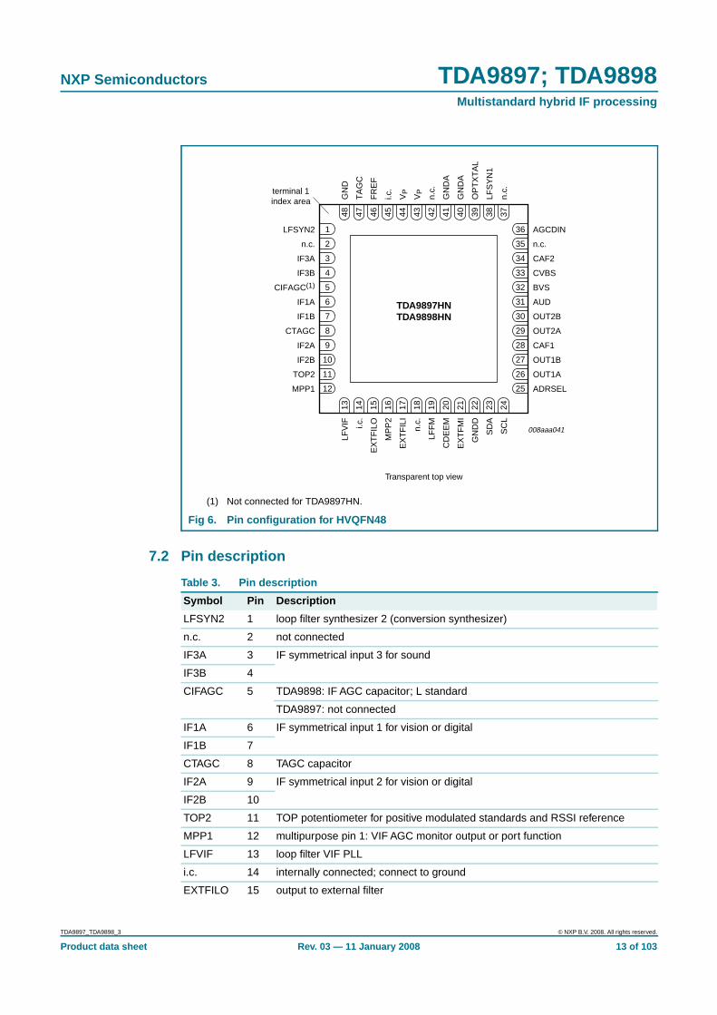
7.2 Pin description
(1) Not connected for TDA9897HN.
Fig 6. Pin configuration for HVQFN48
008aaa041
TDA9897HNTDA9898HN
ADRSEL
TOP2
MPP1
OUT1A
IF2B OUT1B
IF2A CAF1
CTAGC OUT2A
IF1B OUT2B
IF1A AUD
CIFAGC(1) BVS
IF3B CVBS
IF3A CAF2
n.c. n.c.
LFSYN2 AGCDIN
LFV
IF i.c.
EX
TF
ILO
MP
P2
EX
TF
ILI
n.c.
LFF
M
CD
EE
M
EX
TF
MI
GN
DD
SD
A
SC
L
GN
D
TA
GC
FR
EF
i.c.
VP
VP
n.c.
GN
DA
GN
DA
OP
TX
TA
L
LFS
YN
1
n.c.
12 25
11 26
10 27
9 28
8 29
7 30
6 31
5 32
4 33
3 34
2 35
1 36
13 14 15 16 17 18 19 20 21 22 23 24
48 47 46 45 44 43 42 41 40 39 38 37
terminal 1index area
Transparent top view
Table 3. Pin description
Symbol Pin Description
LFSYN2 1 loop filter synthesizer 2 (conversion synthesizer)
n.c. 2 not connected
IF3A 3 IF symmetrical input 3 for sound
IF3B 4
CIFAGC 5 TDA9898: IF AGC capacitor; L standard
TDA9897: not connected
IF1A 6 IF symmetrical input 1 for vision or digital
IF1B 7
CTAGC 8 TAGC capacitor
IF2A 9 IF symmetrical input 2 for vision or digital
IF2B 10
TOP2 11 TOP potentiometer for positive modulated standards and RSSI reference
MPP1 12 multipurpose pin 1: VIF AGC monitor output or port function
LFVIF 13 loop filter VIF PLL
i.c. 14 internally connected; connect to ground
EXTFILO 15 output to external filter
TDA9897_TDA9898_3 © NXP B.V. 2008. All rights reserved.
Product data sheet Rev. 03 — 11 January 2008 13 of 103

NXP Semiconductors TDA9897; TDA9898Multistandard hybrid IF processing
8. Functional description
8.1 IF input switchDifferent signal bandwidth can be handled by using two signal processing chains withindividual gain control.
MPP2 16 multipurpose pin 2: SIF AGC or FM AGC or TAGC or VIF AFC or FM AFCmonitor output
EXTFILI 17 input from external filter
n.c. 18 not connected
LFFM 19 loop filter FM PLL
CDEEM 20 de-emphasis capacitor
EXTFMI 21 external FM input
GNDD 22 digital ground
SDA 23 I2C-bus data input and output
SCL 24 I2C-bus clock input
ADRSEL 25 address select
OUT1A 26 zero IF I or low IF or 2nd sound intercarrier symmetrical output
OUT1B 27
CAF1 28 Direct Current (DC) decoupling capacitor 1
OUT2A 29 zero IF Q or 1st Digital IF (DIF) symmetrical output
OUT2B 30
AUD 31 audio signal output
BVS 32 I2C-bus voltage select
CVBS 33 composite video signal output
CAF2 34 DC decoupling capacitor 2
n.c. 35 not connected
AGCDIN 36 AGC input for DIF amplifier for e.g. input from channel decoder AGC
n.c. 37 not connected
LFSYN1 38 loop filter synthesizer 1 (filter control synthesizer)
OPTXTAL 39 optional quartz input
GNDA 40 analog ground
GNDA 41 analog ground
n.c. 42 not connected
VP 43 supply voltage
VP 44 supply voltage
i.c. 45 internally connected; connect to ground
FREF 46 4 MHz reference input
TAGC 47 TAGC output
GND 48 ground; plateau connection
Table 3. Pin description …continued
Symbol Pin Description
TDA9897_TDA9898_3 © NXP B.V. 2008. All rights reserved.
Product data sheet Rev. 03 — 11 January 2008 14 of 103

NXP Semiconductors TDA9897; TDA9898Multistandard hybrid IF processing
Switch configuration allows independent selection of filter for analog VIF and for analogSIF (used at same time) or DIF.
The switch takes into account correct signal selection for TAGC in the event of VIF andDIF signal processing.
8.2 VIF demodulatorATV demodulation using 6 MHz DVB window (band-pass) filter (for 6 MHz, 7 MHz or8 MHz channel width).
IF frequencies adapted to enable the use of different filter configurations. The Nyquistprocessing is integrated.
For optional use of standard Nyquist filter the integrated Nyquist processing can beswitched off.
Sideband switch supplies selection of lower or upper sideband (e.g. for L-accent).
Equalizer provides optimum pulse response at different standards [e.g. to cope withhigher demands for Liquid Crystal Display (LCD) TV].
Integrated sound traps.
Sound trap reference independent from received 2nd sound IF (reference taken fromintegrated reference synthesizer).
IF level selection provides an optimum adaptation of the demodulator to high linearity orlow noise.
8.3 VIF AGC and tuner AGC
8.3.1 Mode selection of VIF AGC
Peak white AGC for positive modulation mode with adaptation for speed up and black levelAGC (using proven system from TDA9886).
For negative modulation mode equal response times for increasing or decreasing inputlevel (optimum for amplitude fading) or normal peak AGC or ultra fast peak AGC.
8.3.2 VIF AGC monitor
VIF AGC DC voltage monitor output (with expanded internal characteristic).
VIF AGC read out via I2C-bus (for IF level indication) with zero-calibration via TOP setting(TOP setting either via I2C-bus or via TOP potentiometer).
8.3.3 Tuner AGC
Independent integral tuner gain control loop (not nested with VIF AGC). Integralcharacteristic provides high control accuracy.
Accurate setting of tuner control onset (TOP) for integral tuner gain control loop viaI2C-bus.
For L standard, TAGC remains VIF AGC nested, as from field experience in the past thisnarrow-band TAGC gives best performance.
TDA9897_TDA9898_3 © NXP B.V. 2008. All rights reserved.
Product data sheet Rev. 03 — 11 January 2008 15 of 103

NXP Semiconductors TDA9897; TDA9898Multistandard hybrid IF processing
Thus two switchable TAGC systems for negative/DIF and positive modulationimplemented.
L standard TAGC output changed from current output to voltage output, as it is notnecessary to adapt for other than 5 V tuner.
L standard tuner time constant switching integrated (= speed up function in the event ofstep into high input levels), to minimize external application.
For high TOP accuracy at L standard, additional adjustment via optional potentiometer orI2C-bus is provided.
Tuner AGC status bit provided. This function enables TOP alignment without need forTAGC voltage measurement (e.g. for TOP alignment in a complete set, where access tointernal signals is not possible).
8.4 DIF/SIF FM and AM sound AGCExternal AGC control input for DIF. DIF includes 1st IF, zero IF and low IF.
Integrated gain control loop for SIF.
Bandwidth of AGC control for FM SIF related to used SAW bandwidth.
Peak AGC control in the event of FM SIF.
Ultra fast SIF AGC time constant when VIF AGC set to ultra fast mode.
Slow average AGC control in the event of AM sound.
AM sound AGC related to AM sound carrier level.
Fast AM sound AGC in the event of fast VIF AGC (speed up).
SIF AGC DC voltage monitor output with expanded internal characteristic.
8.5 Frequency phase-locked loop for VIFBasic function as previous TDA9887 design.
PLL gating mode for positive and negative modulation, optional.
PLL optimized for either overmodulation or strong multipath.
8.6 DIF/SIF converter stageFrequency conversion with sideband suppression.
Selection mode of upper or lower sideband for pass or suppression.
Suppression around zero for frequency conversion.
I/Q output mode for zero IF conversion.
Conversion mode selection via synthesizer for DIF and radio mode or via VIF FrequencyPhase-Locked Loop (FPLL) for TV QSS sound (FM/AM).
TDA9897_TDA9898_3 © NXP B.V. 2008. All rights reserved.
Product data sheet Rev. 03 — 11 January 2008 16 of 103

NXP Semiconductors TDA9897; TDA9898Multistandard hybrid IF processing
External BP filter (e.g. for 4.5 MHz) for additional filtering, optional.
Bypass mode selection for use of external filter.
Integrated SIF BP tracking filter for chroma suppression.
Integrated tracking filters for LIF and ZIF.
Symmetrical output stages for DIF, ZIF and 2nd SIF.
Second narrow-band gain control loop for 2nd SIF via FM PLL.
8.7 Mono sound demodulator
8.7.1 Narrow-band FM PLL demodulation
Additional external input for either TV or radio intercarrier signal.
FM carrier selection independent from VIF trap, because VIF trap uses reference viasynthesizer.
FM wide and ultra wide mode with adapted loop bandwidth and different selectableFM acquisition window widths to cope with FM overmodulation conditions.
8.7.2 AM sound demodulation
Passive AM sound detector.
L and L-accent standard without SAW switching (done by sideband selection of SIFconverter).
8.8 Audio amplifierDifferent gain settings for FM sound to adapt to different FM deviation.
Switchable de-emphasis for FM sound.
Automatic mute function when FM PLL is unlocked.
Forced mute function.
Output amplifier for AM sound.
8.9 SynthesizerIn DIF mode, the synthesizer supports low and zero IF input frequencies for 34.5 MHz,36 MHz, 44 MHz and 57 MHz center frequencies.
In radio mode, the synthesizer supports 2nd sound intercarrier conversion. A large set ofsynthesizer frequencies in steps of 0.5 MHz enables flexible combination of filter and 2ndIF frequencies.
Synthesizer loop internally adapted to divider ratio range for optimum phase noiserequirement (loop bandwidth).
TDA9897_TDA9898_3 © NXP B.V. 2008. All rights reserved.
Product data sheet Rev. 03 — 11 January 2008 17 of 103

NXP Semiconductors TDA9897; TDA9898Multistandard hybrid IF processing
Synthesizer reference either via 4 MHz crystal or via an external source. Individual pinsfor crystal and external reference allows optimum interface definition and supports use ofcustom reference frequency offset.
8.10 I2C-bus transceiver and slave addressFour different I2C-bus device addresses to enable application with multi-IC use.
I2C-bus transceiver input ports can handle three different I2C-bus voltages.
Read-out functions as TDA9887 plus additional read out of VIF AGC and TAGC status.
9. I2C-bus control
[1] For MAD activation via pin ADRSEL: see Table 4.
Table 4. Slave address detection
Slave address Selectable address bit Pin ADRSEL
A3 A0
MAD1 0 1 GND
MAD2 0 0 VP
MAD3 1 1 resistor to GND
MAD4 1 0 resistor to VP
Table 5. Slave addresses [1]
Slave address Bit
Name Value A6 A5 A4 A3 A2 A1 A0
MAD1 43h 1 0 0 0 0 1 1
MAD2 42h 1 0 0 0 0 1 0
MAD3 4Bh 1 0 0 1 0 1 1
MAD4 4Ah 1 0 0 1 0 1 0
TDA9897_TDA9898_3 © NXP B.V. 2008. All rights reserved.
Product data sheet Rev. 03 — 11 January 2008 18 of 103

NXP Semiconductors TDA9897; TDA9898Multistandard hybrid IF processing
9.1 Read format
[1] If no IF input is applied, then bit AFCWIN can be logic 1 due to the fact that the VCO is forced to the AFCwindow border for fast lock-in behavior.
[2] All standards except M/N standard.
[3] M/N standard.
[4] Typical time constant of FM carrier detection is 50 ms. The minimal recommended wait time for read out is80 ms.
Fig 7. I2C-bus read format (slave transmits data)
Table 6. R1 - data read register 1 bit allocation
7 6 5 4 3 2 1 0
AFCWIN reserved CARRDET AFC4 AFC3 AFC2 AFC1 PONR
Table 7. R1 - data read register 1 bit description
Bit Symbol Description
7 AFCWIN AFC window[1]
1 = VCO in ±1.6 MHz AFC window[2]
1 = VCO in ±0.8 MHz AFC window[3]
0 = VCO out of ±1.6 MHz AFC window[2]
0 = VCO out of ±0.8 MHz AFC window[3]
6 - reserved
5 CARRDET FM carrier detection[4]
1 = detection (FM PLL is locked and level is less than 6 dB belowgain controlled range of FM AGC)
0 = no detection
4 to 1 AFC[4:1] automatic frequency control; see Table 8
0 PONR power-on reset
1 = after power-on reset or after supply breakdown
0 = after a successful reading of the status register
001aad167
A6 to A0 R/W D7 to D0
slave address 1 data (R1) data (R2)
D7 to D0
S BYTE 1 A BYTE 2 A NABYTE 3 P
from master to slave S = START conditionA = acknowledgeNA = not acknowledgeP = STOP conditionfrom slave to master
TDA9897_TDA9898_3 © NXP B.V. 2008. All rights reserved.
Product data sheet Rev. 03 — 11 January 2008 19 of 103

NXP Semiconductors TDA9897; TDA9898Multistandard hybrid IF processing
[1] fnom is the nominal frequency.
[2] In ATV mode f means vision intermediate frequency; in radio mode f means radio intermediate frequency.
Table 8. Automatic frequency control bits [1]
Bit f[2]
AFC4 AFC3 AFC2 AFC1
R1[4] R1[3] R1[2] R1[1]
0 1 1 1 ≤ (fnom − 187.5 kHz)
0 1 1 0 fnom − 162.5 kHz
0 1 0 1 fnom − 137.5 kHz
0 1 0 0 fnom − 112.5 kHz
0 0 1 1 fnom − 87.5 kHz
0 0 1 0 fnom − 62.5 kHz
0 0 0 1 fnom − 37.5 kHz
0 0 0 0 fnom − 12.5 kHz
1 1 1 1 fnom + 12.5 kHz
1 1 1 0 fnom + 37.5 kHz
1 1 0 1 fnom + 62.5 kHz
1 1 0 0 fnom + 87.5 kHz
1 0 1 1 fnom + 112.5 kHz
1 0 1 0 fnom + 137.5 kHz
1 0 0 1 fnom + 162.5 kHz
1 0 0 0 ≥ (fnom + 187.5 kHz)
Table 9. R2 - data read register 2 bit allocation
7 6 5 4 3 2 1 0
reserved TAGC VAGC5 VAGC4 VAGC3 VAGC2 VAGC1 VAGC0
Table 10. R2 - data read register 2 bit description
Bit Symbol Description
7 - reserved
6 TAGC tuner AGC
1 = active
0 = inactive
5 to 0 VAGC[5:0] AGC level detector; VIF AGC in ATV mode, SIF AGC in radio modeand DIF AGC in DTV mode; see Table 11
TDA9897_TDA9898_3 © NXP B.V. 2008. All rights reserved.
Product data sheet Rev. 03 — 11 January 2008 20 of 103

NXP Semiconductors TDA9897; TDA9898Multistandard hybrid IF processing
Table 11. AGC bits (for corresponding AGC characteristic see Figure 12)
Bit Typical∆VAGC(VIF)(V)
VAGC5 VAGC4 VAGC3 VAGC2 VAGC1 VAGC0
R2[5] R2[4] R2[3] R2[2] R2[1] R2[0]
1 1 1 1 1 1 0 (TOP)[1]
1 1 1 1 1 0 −0.04
1 1 1 1 0 1 −0.08
1 1 1 1 0 0 −0.12
1 1 1 0 1 1 −0.16
1 1 1 0 1 0 −0.20
1 1 1 0 0 1 −0.24
1 1 1 0 0 0 −0.28
1 1 0 1 1 1 −0.32
1 1 0 1 1 0 −0.36
1 1 0 1 0 1 −0.40
1 1 0 1 0 0 −0.44
1 1 0 0 1 1 −0.48
1 1 0 0 1 0 −0.52
1 1 0 0 0 1 −0.56
1 1 0 0 0 0 −0.60
1 0 1 1 1 1 −0.64
1 0 1 1 1 0 −0.68
1 0 1 1 0 1 −0.72
1 0 1 1 0 0 −0.76
1 0 1 0 1 1 −0.80
1 0 1 0 1 0 −0.84
1 0 1 0 0 1 −0.88
1 0 1 0 0 0 −0.92
1 0 0 1 1 1 −0.96
1 0 0 1 1 0 −1.00
1 0 0 1 0 1 −1.04
1 0 0 1 0 0 −1.08
1 0 0 0 1 1 −1.12
1 0 0 0 1 0 −1.16
1 0 0 0 0 1 −1.20
1 0 0 0 0 0 −1.24
0 1 1 1 1 1 −1.28
0 1 1 1 1 0 −1.32
0 1 1 1 0 1 −1.36
0 1 1 1 0 0 −1.40
0 1 1 0 1 1 −1.44
0 1 1 0 1 0 −1.48
0 1 1 0 0 1 −1.52
TDA9897_TDA9898_3 © NXP B.V. 2008. All rights reserved.
Product data sheet Rev. 03 — 11 January 2008 21 of 103

NXP Semiconductors TDA9897; TDA9898Multistandard hybrid IF processing
[1] The reference of 0 (TOP) can be adjusted via TOPPOS[4:0] (register W10; see Table 49 and Table 47) orvia potentiometer at pin TOP2.
9.2 Write format
0 1 1 0 0 0 −1.56
0 1 0 1 1 1 −1.60
0 1 0 1 1 0 −1.64
0 1 0 1 0 1 −1.68
0 1 0 1 0 0 −1.72
0 1 0 0 1 1 −1.76
0 1 0 0 1 0 −1.80
0 1 0 0 0 1 −1.84
0 1 0 0 0 0 −1.88
0 0 1 1 1 1 −1.92
0 0 1 1 1 0 −1.96
0 0 1 1 0 1 −2.00
0 0 1 1 0 0 −2.04
0 0 1 0 1 1 −2.08
0 0 1 0 1 0 −2.12
0 0 1 0 0 1 −2.16
0 0 1 0 0 0 −2.20
0 0 0 1 1 1 −2.24
0 0 0 1 1 0 −2.28
0 0 0 1 0 1 −2.32
0 0 0 1 0 0 −2.36
0 0 0 0 1 1 −2.40
0 0 0 0 1 0 −2.44
0 0 0 0 0 1 −2.48
0 0 0 0 0 0 −2.52
Table 11. AGC bits (for corresponding AGC characteristic see Figure 12) …continued
Bit Typical∆VAGC(VIF)(V)
VAGC5 VAGC4 VAGC3 VAGC2 VAGC1 VAGC0
R2[5] R2[4] R2[3] R2[2] R2[1] R2[0]
Fig 8. I2C-bus write format (slave receives data)
001aad166
A6 to A0 R/W A7 to A0 bits 7 to 0
slave address
from master to slave S = START conditionA = acknowledgeP = STOP condition
0 subaddress data 1 data n
bits 7 to 0
from slave to master
S BYTE 1 A BYTE 2 A ABYTE 3 BYTE n A P
TDA9897_TDA9898_3 © NXP B.V. 2008. All rights reserved.
Product data sheet Rev. 03 — 11 January 2008 22 of 103

NXP Semiconductors TDA9897; TDA9898Multistandard hybrid IF processing
9.2.1 Subaddress
[1] The register setting after power-on is not specified.
[2] See Table 17 for detailed description of W1.
[3] See Table 24 for detailed description of W2.
[4] See Table 28 for detailed description of W3.
[5] See Table 30 for detailed description of W4.
[6] See Table 34 for detailed description of W5.
[7] See Table 38 for detailed description of W6.
Table 12. W0 - subaddress register bit allocation
7 6 5 4 3 2 1 0
A7 A6 A5 A4 A3 A2 A1 A0
Table 13. W0 - subaddress register bit description
Bit Symbol Description
7 to 4 A[7:4] has to be set to logic 0
3 to 0 A[3:0] subaddress; see Table 14
Table 14. Subaddress control bits
Bit Mode
A3 A2 A1 A0
0 0 0 0 subaddress for register W1
0 0 0 1 subaddress for register W2
0 0 1 0 subaddress for register W3
0 0 1 1 subaddress for register W4
0 1 0 0 subaddress for register W5
0 1 0 1 subaddress for register W6
0 1 1 0 subaddress for register W7
0 1 1 1 subaddress for register W8
1 0 0 0 subaddress for register W9
1 0 0 1 subaddress for register W10
Table 15. I2C-bus write register overview [1]
Register 7 6 5 4 3 2 1 0
W1[2] RADIO STD1 STD0 TV2 TV1 DUAL FM EXTFIL
W2[3] MOD STD4 STD3 STD2 SB PLL GATE TRAP
W3[4] RESCAR AMUTE FMUTE FMWIDE0 DEEMT DEEM AGAIN1 AGAIN0
W4[5] VIFLEVEL BP MPP2S1 MPP2S0 0 IFIN1 IFIN0 VIFIN
W5[6] FSFREQ1 FSFREQ0 SFREQ5 SFREQ4 SFREQ3 SFREQ2 SFREQ1 SFREQ0
W6[7] TAGC1 TAGC0 AGC2 AGC1 FMWIDE1 TWOFLO 0 DIRECT
W7[8] 0 0 SIFLEVEL VIDLEVEL OPSTATE PORT FILOUTBP NYQOFF
W8[9] 0 0 0 0 EASY3 EASY2 EASY1 EASY0
W9[10] DAGCSLOPE TAGCIS TAGCTC TOPNEG4 TOPNEG3 TOPNEG2 TOPNEG1 TOPNEG0
W10[11] 0 0 XPOTPOS TOPPOS4 TOPPOS3 TOPPOS2 TOPPOS1 TOPPOS0
TDA9897_TDA9898_3 © NXP B.V. 2008. All rights reserved.
Product data sheet Rev. 03 — 11 January 2008 23 of 103

NXP Semiconductors TDA9897; TDA9898Multistandard hybrid IF processing
[8] See Table 41 for detailed description of W7.
[9] See Table 43 for detailed description of W8.
[10] See Table 46 for detailed description of W9.
[11] See Table 49 for detailed description of W10.
9.2.2 Description of data bytes
[1] For description of bit MOD refer to Table 24 and bits FSFREQ[1:0] are described in Table 34.
Table 16. W1 - data write register bit allocation
7 6 5 4 3 2 1 0
RADIO STD1 STD0 TV2 TV1 DUAL FM EXTFIL
Table 17. W1 - data write register bit description
Bit Symbol Description
7 RADIO FM mode
1 = radio
0 = ATV/DTV
6 and 5 STD[1:0] 2nd sound IF; see Table 18 and Table 19
4 and 3 TV[2:1] TV mode
00 = DTV and ZIF
01 = DTV and LIF
10 = not defined
11 = ATV and QSS
2 DUAL ATV and DTV dual mode for channel search; see Table 22
1 = dual (TV2 = 0)
0 = normal
1 and 0 FM and EXTFIL FM and output switching; see Table 21
Table 18. Intercarrier sound BP and FM PLL frequency select for ATV, QSS mode [1]
Bit fFMPLL(MHz)
Sound BP
RADIO MOD STD1 STD0 FSFREQ1 FSFREQ0 TV1
W1[7] W2[7] W1[6] W1[5] W5[7] W5[6] W1[3]
0 1 0 0 X X 1 4.5 M/N standard
0 1 0 1 X X 1 5.5 B/G standard
0 1 1 0 X X 1 6.0 I standard
0 1 1 1 X X 1 6.5 D/K standard
0 0 1 1 X X 1 off L/L-accent standard
TDA9897_TDA9898_3 © NXP B.V. 2008. All rights reserved.
Product data sheet Rev. 03 — 11 January 2008 24 of 103

NXP Semiconductors TDA9897; TDA9898Multistandard hybrid IF processing
[1] For description of bit MOD refer to Table 24 and bits FSFREQ[1:0] are described in Table 34.
[1] For description of bit MOD refer to Table 24 and for BP refer to Table 30.
Table 19. Intercarrier sound BP and FM PLL frequency select for radio, QSS mode [1]
Bit fFMPLL(MHz)
Sound BP
RADIO MOD STD1 STD0 FSFREQ1 FSFREQ0 TV1
W1[7] W2[7] W1[6] W1[5] W5[7] W5[6] W1[3]
1 1 X X 0 0 0 4.5 M/N standard
1 1 X X 0 1 0 5.5 B/G standard
1 1 X X 1 0 0 6.0 I standard
1 1 X X 1 1 0 6.5 D/K standard
1 0 X X X X 0 10.7 RADIO
Table 20. Second sound IF selection for 10.7 MHz [1]
Bit fFMPLL (MHz)
BP MOD RADIO
W4[6] W2[7] W1[7]
0 0 1 10.7
Table 21. 2nd intercarrier and sound input and output switching
MOD FM EXTFIL Mode Input signal selection(input switch)
Signal at OUT1A and OUT1B(output switch)
Mono sounddemodulationW2[7] W1[1] W1[0]
1 0 0 FM sound internal internal BP via FM AGC internal BP
1 0 1 FM sound EXTFILI internal BP external BP
1 1 0 FM sound EXTFMI internal BP external input
1 1 1 FM sound EXTFILI external BP via FM AGC external BP
0 0 0 AM sound not used
0 0 1 AM sound - internal BP internal BP
0 1 0 AM sound - internal BP internal BP
0 1 1 AM sound EXTFILI external BP internal BP
TDA9897_TDA9898_3 © NXP B.V. 2008. All rights reserved.
Product data sheet Rev. 03 — 11 January 2008 25 of 103

NXP Semiconductors TDA9897; TDA9898Multistandard hybrid IF processing
Fig 9. Signal path for intercarrier (2nd SIF) processing
Table 22. Dual mode options
Bit Output mode
TV2 TV1 DIRECT DUAL
W1[4] W1[3] W6[0] W1[2]
X X X 0 all normal mode functions (ATV OR DTV)
0 X 1 1 analog CVBS at pin CVBS AND direct 1st DIF atpins OUT2A and OUT2B
0 0 0 1 analog CVBS at pin CVBS AND digital zero IF I/Q atpins OUT1A, OUT1B and OUT2A, OUT2B
0 1 0 1 analog CVBS at pin CVBS AND digital low IF atpins OUT1A and OUT1B
001aad351
FM PLL
BAND-PASS
BYPASS
W7.1 = 1
external filter output external filter input
EXTFILO
FMswitch
outputswitch
FM AGCamplifier
EXTFILI
OUT1AOUT1B
external FM input
EXTFMI
W7.1 = 0
3 dB
TDA9897_TDA9898_3 © NXP B.V. 2008. All rights reserved.
Product data sheet Rev. 03 — 11 January 2008 26 of 103

NXP Semiconductors TDA9897; TDA9898Multistandard hybrid IF processing
Table 23. W2 - data write register bit allocation
7 6 5 4 3 2 1 0
MOD STD4 STD3 STD2 SB PLL GATE TRAP
Table 24. W2 - data write register bit description
Bit Symbol Description
7 MOD modulation
1 = negative; FM mono sound at ATV and dual mode
0 = positive; AM mono sound at ATV and dual mode
6 to 4 STD[4:2] vision IF; see Table 25
3 SB sideband for sound IF and digital low IF
1 = upper
0 = lower
2 PLL operating modes; see Table 26
1 GATE PLL gating
1 = on
0 = off
0 TRAP sound trap
1 = on
0 = bypass
Table 25. Vision IF
Bit fVIF (MHz) Sideband
NYQOFF MOD STD4 STD3 STD2 TV1 = 1 (QSS)
W7[0] W2[7] W2[6] W2[5] W2[4]
X 0 0 0 0 38.0 low
X 0 0 0 1 38.375 low
X 0 0 1 0 38.875 low
X 0 0 1 1 39.875 low
X 0 1 0 0 32.25 high
0 0 1 0 1 32.625 high
1 0 1 0 1 33.9 -
X 0 1 1 0 33.125 high
X 0 1 1 1 33.625 high
X 1 0 0 0 38.0 low
X 1 0 0 1 38.375 low
X 1 0 1 0 38.875 low
X 1 0 1 1 39.875 low
X 1 1 0 0 45.75 low
X 1 1 0 1 58.75 low
X 1 1 1 0 46.25 low
X 1 1 1 1 59.25 low
TDA9897_TDA9898_3 © NXP B.V. 2008. All rights reserved.
Product data sheet Rev. 03 — 11 January 2008 27 of 103

NXP Semiconductors TDA9897; TDA9898Multistandard hybrid IF processing
Table 26. VIF PLL gating and detector mode
Bit Gating and detector mode
MOD PLL
W2[7] W2[2]
0 0 0 % gating in positive modulation mode (W2[1] = 1)
0 1 36 % gating in positive modulation mode (W2[1] = 1)
1 0 π mode on; optimized for overmodulation in negative modulation mode;fPC = 0 kHz ± 187.5 kHz
1 1 π mode off; optimized for multipath in negative modulation mode;fPC = 0 kHz ± 187.5 kHz
Table 27. W3 - data write register bit allocation
7 6 5 4 3 2 1 0
RESCAR AMUTE FMUTE FMWIDE0 DEEMT DEEM AGAIN1 AGAIN0
Table 28. W3 - data write register bit description
Bit Symbol Description
7 RESCAR video gain correction for residual carrier
1 = 20 % residual carrier
0 = 10 % residual carrier
6 AMUTE auto mute
1 = on
0 = off
5 FMUTE forced mute
1 = on
0 = off
4 FMWIDE0 FM window (W6[3] = 0)
1 = 475 kHz; normal FM phase detector steepness
0 = 237.5 kHz; high FM phase detector steepness
3 DEEMT de-emphasis time
1 = 50 µs
0 = 75 µs
2 DEEM de-emphasis
1 = on
0 = off
1 and 0 AGAIN[1:0] audio gain
00 = 0 dB
01 = −6 dB
10 = −12 dB (only for FM mode)
11 = −18 dB (only for FM mode)
TDA9897_TDA9898_3 © NXP B.V. 2008. All rights reserved.
Product data sheet Rev. 03 — 11 January 2008 28 of 103

NXP Semiconductors TDA9897; TDA9898Multistandard hybrid IF processing
[1] Intercarrier output level based on wide-band AGC of SIF amplifier.
[2] Intercarrier output level based on narrow-band AGC of FM amplifier.
Table 29. W4 - data write register bit allocation
7 6 5 4 3 2 1 0
VIFLEVEL BP MPP2S1 MPP2S0 0 IFIN1 IFIN0 VIFIN
Table 30. W4 - data write register bit description
Bit Symbol Description
7 VIFLEVEL control of internal VIF mixer input level (W1[4] = 1) andOUT1/OUT2 output level; see Table 31
1 = reduced
0 = normal
6 BP SIF/DIF BP
1 = on (bit W6[0] = 0; see Table 38)
0 = bypass
5 and 4 MPP2S[1:0] AGC or AFC output; see Table 32
3 - 0 = fixed value
2 and 1 IFIN[1:0] DIF/SIF input
00 = IF1A/B input
01 = IF3A/B input
10 = not used
11 = IF2A/B input
0 VIFIN VIF input
1 = IF1A/B input
0 = IF2A/B input
Table 31. List of output signals at OUT1 and OUT2
Bit Output signal at
TV2 TV1 DIRECT FM EXTFIL OUT1A, OUT1B OUT2A, OUT2B
W1[4] W1[3] W6[0] W1[1] W1[0]
0 0 0 X X zero IF I zero IF Q
0 1 0 X X low IF off
0 X 1 X X off direct IF
1 X X 0 0 intercarrier[1] off
1 X X 0 1 intercarrier[2] off
1 X X 1 0 intercarrier[2] off
1 X X 1 1 intercarrier[1] off
TDA9897_TDA9898_3 © NXP B.V. 2008. All rights reserved.
Product data sheet Rev. 03 — 11 January 2008 29 of 103

NXP Semiconductors TDA9897; TDA9898Multistandard hybrid IF processing
[1] For bit description of TV1 and TV2 see Table 16 W1[3] and W1[4] and Table 17.
Table 32. Output mode at pin MPP2 for ATV; dual or radio mode
Bit Pin MPP2 output mode
RADIO MPP2S1 MPP2S0
W1[7] W4[5] W4[4]
X 0 0 gain control voltage of FM PLL
X 0 1 gain control voltage of SIF amplifier
X 1 0 TAGC monitor voltage
0 1 1 AFC current output, VIF PLL
1 1 1 AFC current output, radio mode
Table 33. W5 - data write register bit allocation
7 6 5 4 3 2 1 0
FSFREQ1 FSFREQ0 SFREQ5 SFREQ4 SFREQ3 SFREQ2 SFREQ1 SFREQ0
Table 34. W5 - data write register bit description [1]
Bit Symbol Description
7 and 6 FSFREQ[1:0] DTV filter or sound trap selection for video
ATV; sound trap; TV2 = 1
00 = M/N standard (4.5 MHz)
01 = B/G standard (5.5 MHz)
10 = I standard (6.0 MHz)
11 = D/K and L/L-accent standard (6.5 MHz)
DTV (zero IF) ; low-pass cut-off frequency; TV2 = 0 and TV1 = 0
00 = 3.0 MHz
01 = 3.5 MHz
10 = 4.0 MHz
11 = not used
DTV (low IF) ; upper BP cut-off frequency; TV2 = 0 and TV1 = 1
00 = 7.0 MHz
01 = 8.0 MHz
10 = 9.0 MHz
11 = not used
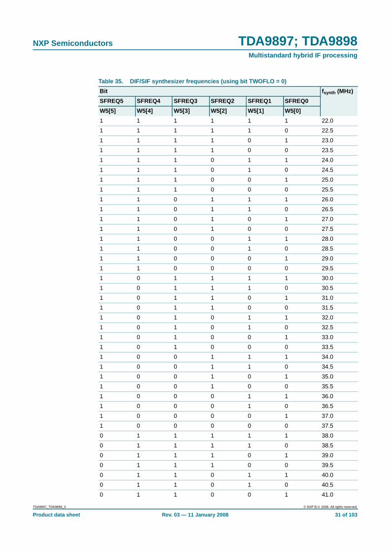
5 to 0 SFREQ[5:0] synthesizer frequencies; see Table 35 and Table 36
TDA9897_TDA9898_3 © NXP B.V. 2008. All rights reserved.
Product data sheet Rev. 03 — 11 January 2008 30 of 103
NXP Semiconductors TDA9897; TDA9898Multistandard hybrid IF processing
Table 35. DIF/SIF synthesizer frequencies (using bit TWOFLO = 0)
Bit fsynth (MHz)
SFREQ5 SFREQ4 SFREQ3 SFREQ2 SFREQ1 SFREQ0
W5[5] W5[4] W5[3] W5[2] W5[1] W5[0]
1 1 1 1 1 1 22.0
1 1 1 1 1 0 22.5
1 1 1 1 0 1 23.0
1 1 1 1 0 0 23.5
1 1 1 0 1 1 24.0
1 1 1 0 1 0 24.5
1 1 1 0 0 1 25.0
1 1 1 0 0 0 25.5
1 1 0 1 1 1 26.0
1 1 0 1 1 0 26.5
1 1 0 1 0 1 27.0
1 1 0 1 0 0 27.5
1 1 0 0 1 1 28.0
1 1 0 0 1 0 28.5
1 1 0 0 0 1 29.0
1 1 0 0 0 0 29.5
1 0 1 1 1 1 30.0
1 0 1 1 1 0 30.5
1 0 1 1 0 1 31.0
1 0 1 1 0 0 31.5
1 0 1 0 1 1 32.0
1 0 1 0 1 0 32.5
1 0 1 0 0 1 33.0
1 0 1 0 0 0 33.5
1 0 0 1 1 1 34.0
1 0 0 1 1 0 34.5
1 0 0 1 0 1 35.0
1 0 0 1 0 0 35.5
1 0 0 0 1 1 36.0
1 0 0 0 1 0 36.5
1 0 0 0 0 1 37.0
1 0 0 0 0 0 37.5
0 1 1 1 1 1 38.0
0 1 1 1 1 0 38.5
0 1 1 1 0 1 39.0
0 1 1 1 0 0 39.5
0 1 1 0 1 1 40.0
0 1 1 0 1 0 40.5
0 1 1 0 0 1 41.0
TDA9897_TDA9898_3 © NXP B.V. 2008. All rights reserved.
Product data sheet Rev. 03 — 11 January 2008 31 of 103

NXP Semiconductors TDA9897; TDA9898Multistandard hybrid IF processing
0 1 1 0 0 0 41.5
0 1 0 1 1 1 42.0
0 1 0 1 1 0 42.5
0 1 0 1 0 1 43.0
0 1 0 1 0 0 43.5
0 1 0 0 1 1 44.0
0 1 0 0 1 0 44.5
0 1 0 0 0 1 45.0
0 1 0 0 0 0 45.5
0 0 1 1 1 1 46.0
0 0 1 1 1 0 46.5
0 0 1 1 0 1 47.0
0 0 1 1 0 0 47.5
0 0 1 0 1 1 48.0
0 0 1 0 1 0 48.5
0 0 1 0 0 1 49.0
0 0 1 0 0 0 49.5
0 0 0 1 1 1 50.0
0 0 0 1 1 0 50.5
0 0 0 1 0 1 51.0
0 0 0 1 0 0 51.5
0 0 0 0 1 1 52.0
0 0 0 0 1 0 52.5
0 0 0 0 0 1 53.0
0 0 0 0 0 0 53.5
Table 36. DIF/SIF synthesizer frequency for zero IF Japan (using bit TWOFLO = 1)
Bit fsynth (MHz)
SFREQ5 SFREQ4 SFREQ3 SFREQ2 SFREQ1 SFREQ0
W5[5] W5[4] W5[3] W5[2] W5[1] W5[0]
1 1 0 0 1 0 57
Table 35. DIF/SIF synthesizer frequencies (using bit TWOFLO = 0) …continued
Bit fsynth (MHz)
SFREQ5 SFREQ4 SFREQ3 SFREQ2 SFREQ1 SFREQ0
W5[5] W5[4] W5[3] W5[2] W5[1] W5[0]
TDA9897_TDA9898_3 © NXP B.V. 2008. All rights reserved.
Product data sheet Rev. 03 — 11 January 2008 32 of 103

NXP Semiconductors TDA9897; TDA9898Multistandard hybrid IF processing
[1] In integral TAGC loop mode the pin TAGC provides sink and source currents for control. TakeOver Point(TOP) is set via register W9 TOPNEG[4:0].
[2] For bit description refer to Table 16 and Table 17.
[1] For bit description of MOD refer to Table 23 W2[7] and Table 24.
Table 37. W6 - data write register bit allocation
7 6 5 4 3 2 1 0
TAGC1 TAGC0 AGC2 AGC1 FMWIDE1 TWOFLO 0 DIRECT
Table 38. W6 - data write register bit description
Bit Symbol Description
7 and 6 TAGC[1:0] tuner AGC mode[1]
00 = TAGC integral loop mode; all currents off
01 = TAGC integral loop mode; source current off
10 = TAGC integral loop mode
11 = TAGC derived from IF AGC; recommended for positivemodulated signals
5 and 4 AGC[2:1] AGC mode and behavior; see Table 39
3 FMWIDE1 FM window
1 = 1 MHz
0 = see Table 28 bit FMWIDE0
2 TWOFLO synthesizer frequency selection
1 = zero IF Japan mode (57 MHz)
0 = synthesizer mode
1 - 0 = fixed value
0 DIRECT direct IF at DTV mode; TV2 = 0[2]
1 = direct IF output
0 = zero IF or low IF output
Table 39. AGC mode and behavior
Bit VIF AGC; MOD = 1[1] SIF AGC
AGC2 AGC1
W6[5] W6[4]
0 0 normal normal
0 1 off (minimum gain) off (minimum gain)
1 0 fast normal
1 1 2nd fast fast
TDA9897_TDA9898_3 © NXP B.V. 2008. All rights reserved.
Product data sheet Rev. 03 — 11 January 2008 33 of 103

NXP Semiconductors TDA9897; TDA9898Multistandard hybrid IF processing
[1] At internal Nyquist processing off (W7[0] = 1) it is mandatory to set the internal video level bit VIDLEVEL tonormal (W7[4] = 0).
Table 40. W7 - data write register bit allocation
7 6 5 4 3 2 1 0
0 0 SIFLEVEL VIDLEVEL OPSTATE PORT FILOUTBP NYQOFF
Table 41. W7 - data write register bit description
Bit Symbol Description
7 and 6 - 0 = fixed value
5 SIFLEVEL SIF level reduction
1 = internal SIF level is reduced by 6 dB (only for AM sound)
0 = internal SIF level is normal
4 VIDLEVEL video level reduction
1 = internal video level is reduced by 6 dB
0 = internal video level is normal
3 OPSTATE output state; PORT = 1
1 = output port is HIGH (external pull-up resistor needed)
0 = output port is LOW
2 PORT port or VIF AGC monitor
1 = pin MPP1 is logic output port; level depends on OPSTATE
0 = pin MPP1 is VIF AGC monitor output; independent on OPSTATE
1 FILOUTBP external filter output signal source; see Figure 9
1 = signal for external filter is obtained behind internal BP filter
0 = signal for external filter is obtained behind SIF mixer
0 NYQOFF internal Nyquist processing
1 = internal Nyquist processing off[1]
0 = internal Nyquist processing on
Table 42. W8 - data write register bit allocation
7 6 5 4 3 2 1 0
0 0 0 0 EASY3 EASY2 EASY1 EASY0
Table 43. W8 - data write register bit description
Bit Symbol Description
7 to 4 - 0 = fixed value
3 to 0 EASY[3:0] easy setting; see Table 44
TDA9897_TDA9898_3 © NXP B.V. 2008. All rights reserved.
Product data sheet Rev. 03 — 11 January 2008 34 of 103

NXP Semiconductors TDA9897; TDA9898Multistandard hybrid IF processing
[1] Access to register W1 to W6 after selection of an easy setting mode would require a transfer of all W1 to W6 register data.
Table 44. Easy setting (to be used for fixed bit set-up only) [1]
Bit Mode orstandard
Name Bit definition (hexadecimal)
EASY3 EASY2 EASY1 EASY0 W1 W2 W3 W4 W5 W6 W7
W8[3] W8[2] W8[1] W8[0]
0 0 0 0 off - - - - - - - -
0 0 0 1 - - - - - - - - -
0 0 1 0 - - - - - - - - -
0 0 1 1 - - - - - - - - -
0 1 0 0 - - - - - - - - -
0 1 0 1 I 6.0 ES2 58 B1 CC 60 80 80 0C
0 1 1 0 B/G 5.5 ES3 38 B1 4C 60 40 80 0C
0 1 1 1 direct IF ES4 08 E1 64 62 00 81 08
1 0 0 0 M Japan 4.5 ES5 18 F1 44 73 00 80 08
1 0 0 1 LIF 6/36 ES6 28 88 60 61 AD 00 0C
1 0 1 0 - - - - - - - - -
1 0 1 1 D/K 6.5 ES8 78 B1 4C 70 C0 80 0C
1 1 0 0 radio 5.5 ES9 BB B8 40 26 6B 00 04
1 1 0 1 - - - - - - - - -
1 1 1 0 L 6.5 ES11 79 33 00 60 C0 C0 0C
1 1 1 1 - - - - - - - - -
Table 45. W9 - data write register bit allocation
7 6 5 4 3 2 1 0
DAGCSLOPE TAGCIS TAGCTC TOPNEG4 TOPNEG3 TOPNEG2 TOPNEG1 TOPNEG0
Table 46. W9 - data write register bit description
Bit Symbol Description
7 DAGCSLOPE AGCDIN input characteristic; see Figure 45
1 = high voltage for high gain
0 = low voltage for high gain
6 TAGCIS tuner AGC IF input
1 = inverse to VIF input
0 = aligned to VIF input
5 TAGCTC tuner AGC time constant
1 = 2nd mode
0 = normal
4 to 0 TOPNEG[4:0] TOP adjustment for integral loop mode; see Table 47
TDA9897_TDA9898_3 © NXP B.V. 2008. All rights reserved.
Product data sheet Rev. 03 — 11 January 2008 35 of 103

NXP Semiconductors TDA9897; TDA9898Multistandard hybrid IF processing
[1] See Table 53 for parameter tuner takeover point accuracy (αacc(set)TOP).
[1] See Table 53 for parameter tuner takeover point accuracy (αacc(set)TOP2).
Table 47. Tuner takeover point adjustment bits W9[4:0]
Bit TOP adjustment (dB µV)
TOPNEG4 TOPNEG3 TOPNEG2 TOPNEG1 TOPNEG0
W9[4] W9[3] W9[2] W9[1] W9[0]
1 1 1 1 1 98.2 typical
: : : : : see Figure 13
1 0 0 0 0 78.7[1]
: : : : : see Figure 13
0 0 0 0 0 57.9 typical
Table 48. W10 - data write register bit allocation
7 6 5 4 3 2 1 0
0 0 XPOTPOS TOPPOS4 TOPPOS3 TOPPOS2 TOPPOS1 TOPPOS0
Table 49. W10 - data write register bit description
Bit Symbol Description
7 and 6 - 0 = fixed value
5 XPOTPOS TOP derived from IF AGC via I2C-bus or potentiometer
1 = TOP adjustment by external potentiometer at pin TOP2
0 = see Table 50
4 to 0 TOPPOS[4:0] TOP adjustment for TAGC derived from IF AGC; see Table 50
Table 50. Tuner takeover point adjustment bits W10[4:0]
Bit TOP adjustment (dB µV)
TOPPOS4 TOPPOS3 TOPPOS2 TOPPOS1 TOPPOS0
W10[4] W10[3] W10[2] W10[1] W10[0]
1 1 1 1 1 99 typical
: : : : : see Figure 13
1 0 0 0 0 81[1]
: : : : : see Figure 13
0 0 0 0 0 61 typical
TDA9897_TDA9898_3 © NXP B.V. 2008. All rights reserved.
Product data sheet Rev. 03 — 11 January 2008 36 of 103

NXP Semiconductors TDA9897; TDA9898Multistandard hybrid IF processing
10. Limiting values
[1] Class 2 according to JESD22-A114.
[2] Class B according to EIA/JESD22-A115.
11. Thermal characteristics
Table 51. Limiting valuesIn accordance with the Absolute Maximum Rating System (IEC 60134).
Symbol Parameter Conditions Min Max Unit
VP supply voltage - 5.5 V
Vn voltage on any other pin all pins except ground 0 VP V
tsc short-circuit time to ground or VP - 10 s
Tstg storage temperature −40 +150 °C
Tamb ambient temperature −20 +70 °C
Tcase case temperature TDA9898HL (LQFP48) - 105 °C
TDA9898HN (HVQFN48) - 115 °C
TDA9897HL (LQFP48) - 105 °C
TDA9897HN (HVQFN48) - 115 °C
Vesd electrostatic discharge voltage human body model [1] - ±3000 V
machine model [2] - ±300 V
Table 52. Thermal characteristics
Symbol Parameter Conditions Typ Unit
Rth(j-a) thermal resistance from junctionto ambient
in free air; 2 layer board
TDA9898HL (LQFP48) 67 K/W
TDA9898HN (HVQFN48) 48 K/W
TDA9897HL (LQFP48) 67 K/W
TDA9897HN (HVQFN48) 48 K/W
Rth(j-c) thermal resistance from junctionto case
TDA9898HL (LQFP48) 19 K/W
TDA9898HN (HVQFN48) 10 K/W
TDA9897HL (LQFP48) 19 K/W
TDA9897HN (HVQFN48) 10 K/W
TDA9897_TDA9898_3 © NXP B.V. 2008. All rights reserved.
Product data sheet Rev. 03 — 11 January 2008 37 of 103

NXP Semiconductors TDA9897; TDA9898Multistandard hybrid IF processing
12. Characteristics
12.1 Analog TV signal processing
Table 53. CharacteristicsVP = 5 V; Tamb = 25 °C; see Table 25 for input frequencies; B/G standard is used for the specification (fPC = 38.375 MHz;fSC = 32.875 MHz; PC / SC = 13 dB; fAF = 400 Hz); input level Vi(IF) = 10 mV (RMS) (sync level for B/G; peak white levelfor L); IF input from 50 Ω via broadband transformer 1 : 1; video modulation: Vestigial SideBand (VSB); residual carrier forB/G is 10 % and for L is 3 %; video signal in accordance with “ITU-T J.63 line 17 and line 330” or “NTC-7 Composite”;internal Nyquist slope switched on (W7[0] = 0); not dual mode; measurements taken in test circuit of Figure 50 and Figure 51;unless otherwise specified.
Symbol Parameter Conditions Min Typ Max Unit
Supply; pin V P
VP supply voltage [1] 4.5 5.0 5.5 V
IP supply current - - 190 mA
Power-on reset
VP(POR) power-on reset supplyvoltage
for start of reset atdecreasing supply voltage
[2] 2.5 3.0 3.5 V
for end of reset atincreasing supply voltage;I2C-bus transmissionenable
[2] - 3.3 4.4 V
VIF amplifier; pins IF1A, IF1B, IF2A and IF2B
VI input voltage - 1.95 - V
Ri(dif) differential input resistance [3] - 2 - kΩ
Ci(dif) differential input capacitance [3] - 3 - pF
Vi(IF)(RMS) RMS IF input voltage lower limit at −1 dB videooutput signal
- 60 100 µV
upper limit at +1 dB videooutput signal
150 190 - mV
permissible overload [4] - - 320 mV
∆GIF IF gain variation difference betweenpicture and sound carrier;within AGC range;∆f = 5.5 MHz
- 0.7 - dB
GVIF(cr) control range VIF gain 60 66 - dB
f−3dB(VIF)l lower VIF cut-off frequency - 15 - MHz
f−3dB(VIF)u upper VIF cut-off frequency - 80 - MHz
FPLL and true synchronous video demodulator [5]
VLFVIF voltage on pin LFVIF (DC) 0.9 - 3.6 V
fVCO(max) maximum VCO frequency fVCO = 2fPC 120 140 - MHz
fVIF VIF frequency see Table 25 - - - MHz
∆fVIF(dah) digital acquisition help VIFfrequency window
related to fVIF
all standards exceptM/N
- ±2.3 - MHz
M/N standard - ±1.8 - MHz
tacq acquisition time BLF(−3dB) = 70 kHz [6] - - 30 ms
TDA9897_TDA9898_3 © NXP B.V. 2008. All rights reserved.
Product data sheet Rev. 03 — 11 January 2008 38 of 103

NXP Semiconductors TDA9897; TDA9898Multistandard hybrid IF processing
Vlock(min)(RMS) RMS minimum lock-involtage
measured on pins IF1Aand IF1B or IF2A andIF2B; maximum IF gain;negative modulationmode W2[7] = 1 and PLLset to overmodulationmode W2[2] = 0 andW2[1] = 0
- 30 70 µV
Tcy(dah) digital acquisition help cycletime
- 64 - µs
tw(dah) digital acquisition help pulsewidth
64 - - µs
Ipul(acq)VIF VIF acquisition pulse current sink or source 21 - 33 µA
KO(VIF) VIF VCO steepness ∆fVIF / ∆VLFVIF - 26 - MHz/V
KD(VIF) VIF phase detectorsteepness
∆IVPLL / ∆ϕVCO(VIF) - 23 - µA/rad
Ioffset(VIF) VIF offset current −1 0 +1 µA
Video output 2 V; pin CVBS [7]
Normal mode (sound carrier trap active) and sound carrier on
Vo(video)(p-p) peak-to-peak video outputvoltage
positive or negativemodulation; see Figure 10
W4[7] = 0; W7[4] = 0 1.7 2.0 2.3 V
W4[7] = 1; W7[4] = 0 1.7 2.0 2.3 V
W4[7] = 0; W7[4] = 1 1.7 2.0 2.3 V
W4[7] = 1; W7[4] = 1 - 2.0 - V
∆Vo(CVBS) CVBS output voltagedifference
difference betweenL and B/G standard
W4[7] = 0; W7[4] = 0 −240 - +240 mV
W4[7] = 1; W7[4] = 0 −240 - +240 mV
W4[7] = 0; W7[4] = 1 −240 - +240 mV
Vvideo/Vsync video voltage to sync voltageratio
2.0 2.33 2.75
Vsyncl sync level voltage W4[7] = 0; W7[4] = 0 1.0 1.2 1.4 V
W4[7] = 1; W7[4] = 0 0.9 1.2 1.5 V
W4[7] = 0; W7[4] = 1 0.9 1.2 1.5 V
Vclip(video)u upper video clipping voltage VP − 1.2 VP − 1 - V
Vclip(video)l lower video clipping voltage - 0.4 0.9 V
RO output resistance [3] - - 30 Ω
Ibias(int) internal bias current (DC) for emitter-follower 1.5 2.0 - mA
Isink(o)(max) maximum output sink current AC and DC 1 - - mA
Table 53. Characteristics …continuedVP = 5 V; Tamb = 25 °C; see Table 25 for input frequencies; B/G standard is used for the specification (fPC = 38.375 MHz;fSC = 32.875 MHz; PC / SC = 13 dB; fAF = 400 Hz); input level Vi(IF) = 10 mV (RMS) (sync level for B/G; peak white levelfor L); IF input from 50 Ω via broadband transformer 1 : 1; video modulation: Vestigial SideBand (VSB); residual carrier forB/G is 10 % and for L is 3 %; video signal in accordance with “ITU-T J.63 line 17 and line 330” or “NTC-7 Composite”;internal Nyquist slope switched on (W7[0] = 0); not dual mode; measurements taken in test circuit of Figure 50 and Figure 51;unless otherwise specified.
Symbol Parameter Conditions Min Typ Max Unit
TDA9897_TDA9898_3 © NXP B.V. 2008. All rights reserved.
Product data sheet Rev. 03 — 11 January 2008 39 of 103

NXP Semiconductors TDA9897; TDA9898Multistandard hybrid IF processing
Isource(o)(max) maximum output sourcecurrent
AC and DC 3.9 - - mA
∆Vo(CVBS) CVBS output voltagedifference
50 dB gain control - - 0.5 dB
30 dB gain control - - 0.1 dB
∆Vblt/VCVBS black level tilt to CVBSvoltage ratio
negative modulation - - 1 %
∆Vblt(v)/VCVBS vertical black level tilt toCVBS voltage ratio
worst case in L standard;vision carrier modulatedby test line [VerticalInterval Test Signal(VITS)] only
- - 3 %
Gdif differential gain “ITU-T J.63 line 330” [8]
B/G standard - - 5 %
L standard - - 7 %
ϕdif differential phase “ITU-T J.63 line 330” [8]
B/G standard - 2 4 deg
L standard - 2 4 deg
(S/N)w weighted signal-to-noise ratio B/G standard; 50 % greyvideo signal; unifiedweighting filter(“ITU-T J.61”);see Figure 20
[9] 53 57 - dB
(S/N)unw unweighted signal-to-noiseratio
M/N standard; 50 IREgrey video signal;see Figure 20
47 51 - dB
VPC(rsd)(RMS) RMS residual picture carriervoltage
fundamental wave andharmonics
- 2 5 mV
∆fPC(p-p) peak-to-peak picture carrierfrequency variation
3 % residual carrier;50 % serration pulses;L standard
[3] - - 12 kHz
∆ϕ phase difference 0 % residual carrier;50 % serration pulses;L standard;L-gating = 0 %
[3] - - 3 %
αH(video) video harmonics suppression AC load: CL < 20 pF,RL > 1 kΩ
[10] 35 40 - dB
αsp spurious suppression [11] 40 - - dB
PSRRCVBS power supply ripple rejectionon pin CVBS
fripple = 70 Hz;video signal; grey level;positive and negativemodulation; see Figure 11
14 20 - dB
Table 53. Characteristics …continuedVP = 5 V; Tamb = 25 °C; see Table 25 for input frequencies; B/G standard is used for the specification (fPC = 38.375 MHz;fSC = 32.875 MHz; PC / SC = 13 dB; fAF = 400 Hz); input level Vi(IF) = 10 mV (RMS) (sync level for B/G; peak white levelfor L); IF input from 50 Ω via broadband transformer 1 : 1; video modulation: Vestigial SideBand (VSB); residual carrier forB/G is 10 % and for L is 3 %; video signal in accordance with “ITU-T J.63 line 17 and line 330” or “NTC-7 Composite”;internal Nyquist slope switched on (W7[0] = 0); not dual mode; measurements taken in test circuit of Figure 50 and Figure 51;unless otherwise specified.
Symbol Parameter Conditions Min Typ Max Unit
TDA9897_TDA9898_3 © NXP B.V. 2008. All rights reserved.
Product data sheet Rev. 03 — 11 January 2008 40 of 103

NXP Semiconductors TDA9897; TDA9898Multistandard hybrid IF processing
M/N standard inclusive Korea; see Figure 21[12]
αripple(resp)f frequency response ripple 0.5 MHz to 2.5 MHz −1 - +1 dB
2.5 MHz to 3.6 MHz −2 - +2 dB
3.6 MHz to 3.8 MHz −3 - +2 dB
3.8 MHz to 4.2 MHz −16 - +2 dB
αSC1 first sound carrier attenuation f = fSC1 = 4.5 MHz 38 - - dB
f = fSC1 ± 60 kHz 29 - - dB
αSC2 second sound carrierattenuation
f = fSC2 = 4.724 MHz 25 - - dB
f = fSC2 ± 60 kHz 16 - - dB
td(grp)CC color carrier group delay time f = 3.58 MHz; includingtransmitter pre-correction;see Figure 22
[13] −75 −50 +75 ns
B/G standard; see Figure 23[12]
αripple(resp)f frequency response ripple 0.5 MHz to 3.2 MHz −1 - +1 dB
3.2 MHz to 4.5 MHz −2 - +2 dB
4.5 MHz to 4.8 MHz −4 - +2 dB
4.8 MHz to 5 MHz −12 - +2 dB
αSC1 first sound carrier attenuation f = fSC1 = 5.5 MHz 35 - - dB
f = fSC1 ± 60 kHz 26 - - dB
αSC2 second sound carrierattenuation
f = fSC2 = 5.742 MHz 25 - - dB
f = fSC2 ± 60 kHz 16 - - dB
αSC(NICAM) NICAM sound carrierattenuation
fcar(NICAM) = 5.85 MHz;f = fcar(NICAM) ± 250 kHz
12 - - dB
α attenuation f = f(N+1)ch = 7 MHz 21 - - dB
f = f(N+1)ch ± 750 kHz 5 - - dB
td(grp)CC color carrier group delay time f = 4.43 MHz; includingtransmitter pre-correction;see Figure 24
[13] −75 −10 +75 ns
I standard; see Figure 25[12]
αripple(resp)f frequency response ripple 0.5 MHz to 3.2 MHz −1 - +1 dB
3.2 MHz to 4.5 MHz −2 - +2 dB
4.5 MHz to 5 MHz −4 - +2 dB
5 MHz to 5.5 MHz −12 - +2 dB
αSC1 first sound carrier attenuation f = fSC1 = 6.0 MHz 35 - - dB
f = fSC1 ± 60 kHz 26 - - dB
αSC(NICAM) NICAM sound carrierattenuation
fcar(NICAM) = 6.55 MHz;f = fcar(NICAM) ± 250 kHz
12 - - dB
Table 53. Characteristics …continuedVP = 5 V; Tamb = 25 °C; see Table 25 for input frequencies; B/G standard is used for the specification (fPC = 38.375 MHz;fSC = 32.875 MHz; PC / SC = 13 dB; fAF = 400 Hz); input level Vi(IF) = 10 mV (RMS) (sync level for B/G; peak white levelfor L); IF input from 50 Ω via broadband transformer 1 : 1; video modulation: Vestigial SideBand (VSB); residual carrier forB/G is 10 % and for L is 3 %; video signal in accordance with “ITU-T J.63 line 17 and line 330” or “NTC-7 Composite”;internal Nyquist slope switched on (W7[0] = 0); not dual mode; measurements taken in test circuit of Figure 50 and Figure 51;unless otherwise specified.
Symbol Parameter Conditions Min Typ Max Unit
TDA9897_TDA9898_3 © NXP B.V. 2008. All rights reserved.
Product data sheet Rev. 03 — 11 January 2008 41 of 103

NXP Semiconductors TDA9897; TDA9898Multistandard hybrid IF processing
td(grp)CC color carrier group delay time f = 4.43 MHz;see Figure 26
[13] −75 −15 +75 ns
D/K standard; see Figure 27[12]
αripple(resp)f frequency response ripple 0.5 MHz to 3.1 MHz −1 - +1 dB
3.1 MHz to 4.5 MHz −2 - +2 dB
4.5 MHz to 4.8 MHz −4 - +2 dB
4.8 MHz to 5.1 MHz −6 - +2 dB
αSC1 first sound carrier attenuation f = fSC1 = 6.5 MHz 35 - - dB
f = fSC1 ± 60 kHz 26 - - dB
αSC2(us) second sound carrierattenuation (upper side)
f = fSC2 = 6.742 MHz 25 - - dB
f = fSC2 ± 60 kHz 16 - - dB
αSC2(ls) second sound carrierattenuation (lower side)
f = fSC2 = 6.258 MHz 25 - - dB
f = fSC2 ± 60 kHz 16 - - dB
αSC(NICAM) NICAM sound carrierattenuation
fcar(NICAM) = 5.85 MHz;f = fcar(NICAM) ± 250 kHz
6 - - dB
td(grp)CC color carrier group delay time f = 4.28 MHz; includingtransmitter pre-correction;see Figure 28
[13] −50 0 +100 ns
L standard; see Figure 29[12]
αripple(resp)f frequency response ripple 0.5 MHz to 3.2 MHz −1 - +1 dB
3.2 MHz to 4.5 MHz −2 - +2 dB
4.5 MHz to 4.8 MHz −4 - +2 dB
4.8 MHz to 5.3 MHz −12 - +2 dB
αSC(NICAM) NICAM sound carrierattenuation
fcar(NICAM) = 5.85 MHz;f = fcar(NICAM) ± 250 kHz
5 - - dB
αSC(AM) AM sound carrier attenuation f = fSC(AM) = 6.5 MHz 38 - - dB
f = fSC(AM) ± 30 kHz 29 - - dB
td(grp)CC color carrier group delay time f = 4.28 MHz; includingtransmitter pre-correction;see Figure 30
−75 −5 +75 ns
Video output 1.1 V; pin CVBS
Trap bypass mode and sound carrier off[12]
Vo(video)(p-p) peak-to-peak video outputvoltage
see Figure 10 - 1.1 - V
Vsyncl sync level voltage - 1.5 - V
Vclip(video)u upper video clipping voltage VP − 1.1 VP − 1 - V
Vclip(video)l lower video clipping voltage - 0.4 0.9 V
Bvideo(−3dB) −3 dB video bandwidth AC load: CL < 20 pF,RL > 1 kΩ
6 8 - MHz
Table 53. Characteristics …continuedVP = 5 V; Tamb = 25 °C; see Table 25 for input frequencies; B/G standard is used for the specification (fPC = 38.375 MHz;fSC = 32.875 MHz; PC / SC = 13 dB; fAF = 400 Hz); input level Vi(IF) = 10 mV (RMS) (sync level for B/G; peak white levelfor L); IF input from 50 Ω via broadband transformer 1 : 1; video modulation: Vestigial SideBand (VSB); residual carrier forB/G is 10 % and for L is 3 %; video signal in accordance with “ITU-T J.63 line 17 and line 330” or “NTC-7 Composite”;internal Nyquist slope switched on (W7[0] = 0); not dual mode; measurements taken in test circuit of Figure 50 and Figure 51;unless otherwise specified.
Symbol Parameter Conditions Min Typ Max Unit
TDA9897_TDA9898_3 © NXP B.V. 2008. All rights reserved.
Product data sheet Rev. 03 — 11 January 2008 42 of 103

NXP Semiconductors TDA9897; TDA9898Multistandard hybrid IF processing
(S/N)w weighted signal-to-noise ratio B/G standard; 50 % greyvideo signal; unifiedweighting filter(“ITU-T J.61”);see Figure 20
[9] 54 - - dB
(S/N)unw unweighted signal-to-noiseratio
M/N standard; 50 IREgrey video signal;see Figure 20
[9] 47 51 - dB
Loop filter synthesizer; pin LFSYN1
VLFSYN1 voltage on pin LFSYN1 1.0 - 3.5 V
Isource(o)PD(max) maximum phase detectoroutput source current
- - 65 µA
Isink(o)PD(max) maximum phase detectoroutput sink current
- - 65 µA
KO VCO steepness - 3.75 - MHz/V
KD phase detector steepness - 9 - µA/rad
Pin MPP1 operating as VIF AGC voltage monitor
Vmonitor(VIFAGC) VIF AGC monitor voltage [3] 0.5 - 4.5 V
VAGC AGC voltage see Figure 12; Vi(IF) set to
1 mV (60 dBµV) 2.2 - 2.6 V
10 mV (80 dBµV) 2.5 - 3.1 V
200 mV (106 dBµV) 3 - 4 V
Io(max) maximum output current sink or source 10 - - µA
Table 53. Characteristics …continuedVP = 5 V; Tamb = 25 °C; see Table 25 for input frequencies; B/G standard is used for the specification (fPC = 38.375 MHz;fSC = 32.875 MHz; PC / SC = 13 dB; fAF = 400 Hz); input level Vi(IF) = 10 mV (RMS) (sync level for B/G; peak white levelfor L); IF input from 50 Ω via broadband transformer 1 : 1; video modulation: Vestigial SideBand (VSB); residual carrier forB/G is 10 % and for L is 3 %; video signal in accordance with “ITU-T J.63 line 17 and line 330” or “NTC-7 Composite”;internal Nyquist slope switched on (W7[0] = 0); not dual mode; measurements taken in test circuit of Figure 50 and Figure 51;unless otherwise specified.
Symbol Parameter Conditions Min Typ Max Unit
TDA9897_TDA9898_3 © NXP B.V. 2008. All rights reserved.
Product data sheet Rev. 03 — 11 January 2008 43 of 103

NXP Semiconductors TDA9897; TDA9898Multistandard hybrid IF processing
tresp response time increasing VIF step;negative modulation
[14]
normal mode - 4.3 - µs/dB
fast mode - 1.5 - µs/dB
increasing VIF step;positive modulation;normal mode
[14] - 130 - µs/dB
decreasing VIF step;negative modulation
[14]
normal mode - 1.9 - ms/dB
fast normal mode - 0.08 - ms/dB
2nd mode - 0.25 - ms/dB
fast 2nd mode - 0.01 - ms/dB
decreasing VIF step;positive modulation
[14]
20 dB - 890 - ms
fast mode - 2.6 - ms/dB
normal mode - 143 - ms/dB
αth(fast)VIF VIF fast mode threshold L standard −10 −6 −2 dB
∆VVAGC(step) VIF AGC voltage difference(step)
see Table 11 - 40 - mV/bit
Pin MPP1 operating as open-collector output port
VOL LOW-level output voltage I = 2 mA (sink) - - 0.4 V
Isink(o) output sink current W7[3] = 0 - - 3 mA
W7[3] = 1 - - 10 µA
VOH HIGH-level output voltage - - VP + 0.5 V
VIF AGC; pin CIFAGC
Ich(max) maximum charge current L standard 75 100 125 µA
Ich(add) additional charge current L standard: in the event ofmissing VITS pulses andno white video content
- 100 - nA
Idch discharge current L standard; normal mode - 35 - nA
L standard; fast mode - 1.8 - µA
Table 53. Characteristics …continuedVP = 5 V; Tamb = 25 °C; see Table 25 for input frequencies; B/G standard is used for the specification (fPC = 38.375 MHz;fSC = 32.875 MHz; PC / SC = 13 dB; fAF = 400 Hz); input level Vi(IF) = 10 mV (RMS) (sync level for B/G; peak white levelfor L); IF input from 50 Ω via broadband transformer 1 : 1; video modulation: Vestigial SideBand (VSB); residual carrier forB/G is 10 % and for L is 3 %; video signal in accordance with “ITU-T J.63 line 17 and line 330” or “NTC-7 Composite”;internal Nyquist slope switched on (W7[0] = 0); not dual mode; measurements taken in test circuit of Figure 50 and Figure 51;unless otherwise specified.
Symbol Parameter Conditions Min Typ Max Unit
TDA9897_TDA9898_3 © NXP B.V. 2008. All rights reserved.
Product data sheet Rev. 03 — 11 January 2008 44 of 103

NXP Semiconductors TDA9897; TDA9898Multistandard hybrid IF processing
Tuner AGC; pin TAGC
Integral TAGC loop mode (W6[7:6] = 10); TAGC is current output; applicable for negative modulation only; unmodulated VIF;see Table 46 and Figure 13
Vi(IF)(RMS) RMS IF input voltage at starting point of tunerAGC takeover;Isink(TAGC) = 100 µA
W9[4:0] = 0 0000 - 57.9 - dBµV
W9[4:0] = 1 0000 - 78.7 - dBµV
W9[4:0] = 1 1111 - 98.2 - dBµV
αacc(set)TOP TOP setting accuracy −2 - +2 dB
Isource source current TAGC charge current
normal mode;W9[5] = 0
0.2 0.3 0.4 µA
2nd normal mode;W9[5] = 1
1.9 2.3 2.7 µA
fast mode activated byinternal level detector;W9[5] = 0
7 11 15 µA
2nd fast mode activatedby internal leveldetector; W9[5] = 1
60 90 120 µA
Isink sink current TAGC discharge current;VTAGC = 1 V
400 500 600 µA
∆αacc(set)TOP/∆T TOP setting accuracyvariation with temperature
W9[4:0] = 1 0000 - - 0.02 dB/K
RL load resistance [3] 50 - - MΩ
Vsat(u) upper saturation voltage pin operating as currentoutput
VP − 0.3 - - V
Vsat(l) lower saturation voltage pin operating as currentoutput
- - 0.3 V
αth(fast)AGC AGC fast mode threshold activated by internal fastAGC detector; I2C-bussetting corresponds toW9[4:0] = 1 0000
[3] 6 8 10 dB
td delay time before activating; Vi(IF)below αth(fast)AGC
40 60 80 ms
Table 53. Characteristics …continuedVP = 5 V; Tamb = 25 °C; see Table 25 for input frequencies; B/G standard is used for the specification (fPC = 38.375 MHz;fSC = 32.875 MHz; PC / SC = 13 dB; fAF = 400 Hz); input level Vi(IF) = 10 mV (RMS) (sync level for B/G; peak white levelfor L); IF input from 50 Ω via broadband transformer 1 : 1; video modulation: Vestigial SideBand (VSB); residual carrier forB/G is 10 % and for L is 3 %; video signal in accordance with “ITU-T J.63 line 17 and line 330” or “NTC-7 Composite”;internal Nyquist slope switched on (W7[0] = 0); not dual mode; measurements taken in test circuit of Figure 50 and Figure 51;unless otherwise specified.
Symbol Parameter Conditions Min Typ Max Unit
TDA9897_TDA9898_3 © NXP B.V. 2008. All rights reserved.
Product data sheet Rev. 03 — 11 January 2008 45 of 103

NXP Semiconductors TDA9897; TDA9898Multistandard hybrid IF processing
TAGC loop based on VIF AGC (W6[7:6] = 11); TAGC is voltage output; applicable for TV mode: positive modulation andoptional for negative modulation); see Table 49; Figure 13 and Figure 14
Vi(IF)(RMS) RMS IF input voltage at starting point of tunerAGC takeover;VTAGC = 3.5 V
RTOP2 = 22 kΩ orW10[5:0] = 00 0000
- 61 - dBµV
RTOP2 = 10 kΩ orW10[5:0] = 01 0000
- 81 - dBµV
RTOP2 = 0 kΩ - 96 - dBµV
W10[5:0] = 01 1111 - 99 - dBµV
αacc(set)TOP2 TOP2 setting accuracy −6 - +6 dB
∆αacc(set)TOP2/∆T TOP2 setting accuracyvariation with temperature
VTAGC = 3.5 V - 0.03 0.07 dB/K
VO output voltage no tuner gain reduction 4.5 - VP V
maximum tuner gainreduction
0.2 - 0.6 V
∆Gslip(TAGC) TAGC slip gain offset tuner gain voltage from0.6 V to 3.5 V
3 5 8 dB
TOP adjust 2; pin TOP2; IF based TAGC loop mode; see Figure 14
VTOP2 voltage on pin TOP2 (DC) pin open-circuit - 3.5 - V
RI input resistance - 27 - kΩ
RTOP2 resistance on pin TOP2 adjustment of VIF AGCbased TAGC loop
W10[5] = 1; externalresistor operation
0 - 22 kΩ
W10[5] = 0; forcedI2C-bus operation
100 - - kΩ
Pin CTAGC
VCTAGC voltage on pin CTAGC [3] 0.2 - 0.55VP V
IL leakage current sink [3] - - 10 nA
source [3] - - 10 nA
Control current or voltage monitor output; pin MPP2
General
Vsat(u) upper saturation voltage VP − 0.8 VP − 0.5 - V
Vsat(l) lower saturation voltage - 0.5 0.8 V
Table 53. Characteristics …continuedVP = 5 V; Tamb = 25 °C; see Table 25 for input frequencies; B/G standard is used for the specification (fPC = 38.375 MHz;fSC = 32.875 MHz; PC / SC = 13 dB; fAF = 400 Hz); input level Vi(IF) = 10 mV (RMS) (sync level for B/G; peak white levelfor L); IF input from 50 Ω via broadband transformer 1 : 1; video modulation: Vestigial SideBand (VSB); residual carrier forB/G is 10 % and for L is 3 %; video signal in accordance with “ITU-T J.63 line 17 and line 330” or “NTC-7 Composite”;internal Nyquist slope switched on (W7[0] = 0); not dual mode; measurements taken in test circuit of Figure 50 and Figure 51;unless otherwise specified.
Symbol Parameter Conditions Min Typ Max Unit
TDA9897_TDA9898_3 © NXP B.V. 2008. All rights reserved.
Product data sheet Rev. 03 — 11 January 2008 46 of 103

NXP Semiconductors TDA9897; TDA9898Multistandard hybrid IF processing
AFC (current output)
Io output current sink or source;see Figure 17 andFigure 18
[15][16]
100 kHz VIF deviation 80 - 160 µA
200 kHz VIF deviation 160 200 240 µA
1.5 MHz VIF deviation 160 - 240 µA
AFC TV mode
∆IAFC/∆fVIF change of AFC current withVIF frequency
[16] 0.85 1.05 1.25 µA/kHz
fVIFacc(dig) digital accuracy of VIFfrequency
read-out via I2C-bus;R1[4:1] = f0; fref = 4 MHz
[17] −20 - +20 kHz
fVIFacc(a) analog accuracy of VIFfrequency
IAFC = 0 A; fref = 4 MHz [17] −20 - +20 kHz
AFC radio mode
∆IAFC/∆fRIF change of AFC current withRIF frequency
[16] 0.85 1.05 1.25 µA/kHz
fRIFacc(dig) digital accuracy of RIFfrequency
read-out via I2C-bus;R1[4:1] = f0; fref = 4 MHz
[17] −10 - +10 kHz
fRIFacc(a) analog accuracy of RIFfrequency
IAFC = 0 A; fref = 4 MHz [17] −10 - +10 kHz
AGC monitor (voltage output)
Gv voltage gain voltage on pin MPP2 tointernal control voltage;see Table 32
- 0 - dB
SIF AGC - 6 - dB
FM AGC - 6 - dB
TAGC - 0 - dB
Io(max) maximum output current sink or source 350 - - µA
SIF amplifier; pins IF3A and IF3B or pins IF1A and IF1B or pins IF2A and IF2B
VI input voltage - 1.95 - V
Ri(dif) differential input resistance - 2 - kΩ
Ci(dif) differential input capacitance - 3 - pF
Table 53. Characteristics …continuedVP = 5 V; Tamb = 25 °C; see Table 25 for input frequencies; B/G standard is used for the specification (fPC = 38.375 MHz;fSC = 32.875 MHz; PC / SC = 13 dB; fAF = 400 Hz); input level Vi(IF) = 10 mV (RMS) (sync level for B/G; peak white levelfor L); IF input from 50 Ω via broadband transformer 1 : 1; video modulation: Vestigial SideBand (VSB); residual carrier forB/G is 10 % and for L is 3 %; video signal in accordance with “ITU-T J.63 line 17 and line 330” or “NTC-7 Composite”;internal Nyquist slope switched on (W7[0] = 0); not dual mode; measurements taken in test circuit of Figure 50 and Figure 51;unless otherwise specified.
Symbol Parameter Conditions Min Typ Max Unit
TDA9897_TDA9898_3 © NXP B.V. 2008. All rights reserved.
Product data sheet Rev. 03 — 11 January 2008 47 of 103

NXP Semiconductors TDA9897; TDA9898Multistandard hybrid IF processing
Vi(SIF)(RMS) RMS SIF input voltage FM mode; −3 dB atintercarrier outputpins OUT1A and OUT1B;without FM AGC;see Table 21
- 60 100 µV
AM mode; −3 dB atAF output pin AUD
- 40 70 µV
FM mode; +1 dB atintercarrier outputpins OUT1A and OUT1B;without FM AGC;see Table 21
150 190 - mV
AM mode; +1 dB atAF output pin AUD
70 140 - mV
permissible overload - - 320 mV
GSIF(cr) control range SIF gain FM and AM mode 60 66 - dB
f−3dB(SIF)l lower SIF cut-off frequency - 7 - MHz
f−3dB(SIF)u upper SIF cut-off frequency - 80 - MHz
SIF AGC detector; pin MPP2; see Figure 16
tresp response time increasing or decreasingSIF step of 20 dB;AM mode; fast AGC
increasing - 8 - ms
decreasing - 25 - ms
increasing or decreasingSIF step of 20 dB;AM mode; slow AGC
increasing - 80 - ms
decreasing - 250 - ms
increasing or decreasingSIF step of 20 dB;FM mode; normal AGC
increasing - 0.3 - ms
decreasing - 20 - ms
increasing or decreasingSIF step of 20 dB;FM mode; fast AGC
increasing - 0.1 - ms
decreasing - 4 - ms
Table 53. Characteristics …continuedVP = 5 V; Tamb = 25 °C; see Table 25 for input frequencies; B/G standard is used for the specification (fPC = 38.375 MHz;fSC = 32.875 MHz; PC / SC = 13 dB; fAF = 400 Hz); input level Vi(IF) = 10 mV (RMS) (sync level for B/G; peak white levelfor L); IF input from 50 Ω via broadband transformer 1 : 1; video modulation: Vestigial SideBand (VSB); residual carrier forB/G is 10 % and for L is 3 %; video signal in accordance with “ITU-T J.63 line 17 and line 330” or “NTC-7 Composite”;internal Nyquist slope switched on (W7[0] = 0); not dual mode; measurements taken in test circuit of Figure 50 and Figure 51;unless otherwise specified.
Symbol Parameter Conditions Min Typ Max Unit
TDA9897_TDA9898_3 © NXP B.V. 2008. All rights reserved.
Product data sheet Rev. 03 — 11 January 2008 48 of 103

NXP Semiconductors TDA9897; TDA9898Multistandard hybrid IF processing
VAGC(SIF) SIF AGC voltage FM mode
VSIF = 100 µV 1.5 - 2.4 V
VSIF = 10 mV 2.6 - 3.4 V
VSIF = 140 mV 3.3 - VP V
AM mode
VSIF = 100 µV 1.5 - 2.4 V
VSIF = 10 mV 2.9 - 3.9 V
VSIF = 140 mV 3.3 - VP V
Conversion synthesizer PLL; pin LFSYN2 (radio mode)
VLFSYN2 voltage on pin LFSYN2 1 - 3 V
KO VCO steepness ∆fVCO / ∆VLFSYN2 - 31 - MHz/V
KD phase detector steepness ∆ILFSYN2 / ∆ϕVCO;see Table 57;fVCO selection:
22 MHz to 29.5 MHz - 32 - µA/rad
30 MHz to 37.5 MHz - 38 - µA/rad
38 MHz to 45.5 MHz - 47 - µA/rad
46 MHz to 53.5 MHz - 61 - µA/rad
57 MHz - 61 - µA/rad
Io(PD) phase detector output current sink or source;fVCO selection:
22 MHz to 29.5 MHz - 200 - µA
30 MHz to 37.5 MHz - 238 - µA
38 MHz to 45.5 MHz - 294 - µA
46 MHz to 53.5 MHz - 384 - µA
57 MHz - 384 - µA
ϕn(synth) synthesizer phase noise with 4 MHz crystaloscillator reference
at 1 kHz [3] 89 99 - dBc/Hz
at 10 kHz [3] 89 99 - dBc/Hz
at 100 kHz [3] 98 102 - dBc/Hz
at 1.4 MHz [3] 115 119 - dBc/Hz
αsp spurious suppression multiple of ∆f = 500 kHz [3] 50 - - dBc
IL leakage current synthesizer spuriousperformance > 50 dBc
[3] - - 10 nA
Table 53. Characteristics …continuedVP = 5 V; Tamb = 25 °C; see Table 25 for input frequencies; B/G standard is used for the specification (fPC = 38.375 MHz;fSC = 32.875 MHz; PC / SC = 13 dB; fAF = 400 Hz); input level Vi(IF) = 10 mV (RMS) (sync level for B/G; peak white levelfor L); IF input from 50 Ω via broadband transformer 1 : 1; video modulation: Vestigial SideBand (VSB); residual carrier forB/G is 10 % and for L is 3 %; video signal in accordance with “ITU-T J.63 line 17 and line 330” or “NTC-7 Composite”;internal Nyquist slope switched on (W7[0] = 0); not dual mode; measurements taken in test circuit of Figure 50 and Figure 51;unless otherwise specified.
Symbol Parameter Conditions Min Typ Max Unit
TDA9897_TDA9898_3 © NXP B.V. 2008. All rights reserved.
Product data sheet Rev. 03 — 11 January 2008 49 of 103

NXP Semiconductors TDA9897; TDA9898Multistandard hybrid IF processing
PSRR power supply ripple rejection residual spurious atnominal differential outputvoltage dependent onpower supply ripple at70 Hz; see Figure 11
- 50 - dB
Single reference QSS intercarrier mixer; pins OUT1A and OUT1B
VOUT1A voltage on pin OUT1A (DC) 1.8 2.0 2.2 V
VOUT1B voltage on pin OUT1B (DC) 1.8 2.0 2.2 V
Ibias(int) internal bias current (DC) for emitter-follower 2.0 2.5 - mA
Isink(o)(max) maximum output sink current DC and AC 1.4 1.7 - mA
Isource(o)(max) maximum output sourcecurrent
DC and AC; with externalresistor to GND
3.0 - - mA
RO output resistance output active;single-ended to GND
- - 25 Ω
output inactive; internalresistance to GND
- 800 - Ω
Vo(RMS) RMS output voltage IF intercarriersingle-ended to GND;SC1 on; SC2 off
90 140 180 mV
IF intercarriersingle-ended to GND;L standard;without modulation;BP on
W7[5] = 0 45 70 90 mV
W7[5] = 1 20 35 45 mV
f−3dB(ic)u upper intercarrier cut-offfrequency
internal sound band-passoff
11 15 - MHz
αimage image rejection band-pass off;−8 MHz to 0 MHz
24 28 - dB
Vinterf(RMS) RMS interference voltage fundamental wave andharmonics
- 2 5 mV
AM intercarrier from pin EXTFILI to pins OUT1A and OUT1B
G gain IF intercarrier; L standard;without modulation
- 5 - dB
Table 53. Characteristics …continuedVP = 5 V; Tamb = 25 °C; see Table 25 for input frequencies; B/G standard is used for the specification (fPC = 38.375 MHz;fSC = 32.875 MHz; PC / SC = 13 dB; fAF = 400 Hz); input level Vi(IF) = 10 mV (RMS) (sync level for B/G; peak white levelfor L); IF input from 50 Ω via broadband transformer 1 : 1; video modulation: Vestigial SideBand (VSB); residual carrier forB/G is 10 % and for L is 3 %; video signal in accordance with “ITU-T J.63 line 17 and line 330” or “NTC-7 Composite”;internal Nyquist slope switched on (W7[0] = 0); not dual mode; measurements taken in test circuit of Figure 50 and Figure 51;unless otherwise specified.
Symbol Parameter Conditions Min Typ Max Unit
TDA9897_TDA9898_3 © NXP B.V. 2008. All rights reserved.
Product data sheet Rev. 03 — 11 January 2008 50 of 103
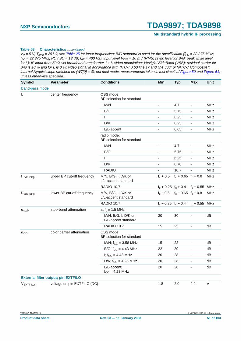
NXP Semiconductors TDA9897; TDA9898Multistandard hybrid IF processing
Band-pass mode
fc center frequency QSS mode;BP selection for standard
M/N - 4.7 - MHz
B/G - 5.75 - MHz
I - 6.25 - MHz
D/K - 6.25 - MHz
L/L-accent - 6.05 - MHz
radio mode;BP selection for standard
M/N - 4.7 - MHz
B/G - 5.75 - MHz
I - 6.25 - MHz
D/K - 6.78 - MHz
RADIO - 10.7 - MHz
f−3dB(BP)u upper BP cut-off frequency M/N, B/G, I, D/K orL/L-accent standard
fc + 0.5 fc + 0.65 fc + 0.8 MHz
RADIO 10.7 fc + 0.25 fc + 0.4 fc + 0.55 MHz
f−3dB(BP)l lower BP cut-off frequency M/N, B/G, I, D/K orL/L-accent standard
fc − 0.5 fc − 0.65 fc − 0.8 MHz
RADIO 10.7 fc − 0.25 fc − 0.4 fc − 0.55 MHz
αstpb stop-band attenuation at fc ± 1.5 MHz
M/N, B/G, I, D/K orL/L-accent standard
20 30 - dB
RADIO 10.7 15 25 - dB
αCC color carrier attenuation QSS mode;BP selection for standard
M/N; fCC = 3.58 MHz 15 23 - dB
B/G; fCC = 4.43 MHz 22 30 - dB
I; fCC = 4.43 MHz 20 28 - dB
D/K; fCC = 4.28 MHz 20 28 - dB
L/L-accent;fCC = 4.28 MHz
20 28 - dB
External filter output; pin EXTFILO
VEXTFILO voltage on pin EXTFILO (DC) 1.8 2.0 2.2 V
Table 53. Characteristics …continuedVP = 5 V; Tamb = 25 °C; see Table 25 for input frequencies; B/G standard is used for the specification (fPC = 38.375 MHz;fSC = 32.875 MHz; PC / SC = 13 dB; fAF = 400 Hz); input level Vi(IF) = 10 mV (RMS) (sync level for B/G; peak white levelfor L); IF input from 50 Ω via broadband transformer 1 : 1; video modulation: Vestigial SideBand (VSB); residual carrier forB/G is 10 % and for L is 3 %; video signal in accordance with “ITU-T J.63 line 17 and line 330” or “NTC-7 Composite”;internal Nyquist slope switched on (W7[0] = 0); not dual mode; measurements taken in test circuit of Figure 50 and Figure 51;unless otherwise specified.
Symbol Parameter Conditions Min Typ Max Unit
TDA9897_TDA9898_3 © NXP B.V. 2008. All rights reserved.
Product data sheet Rev. 03 — 11 January 2008 51 of 103

NXP Semiconductors TDA9897; TDA9898Multistandard hybrid IF processing
VEXTFILO(p-p) peak-to-peak voltage onpin EXTFILO
IF intercarrier; SC1 on;SC2 off
420 620 820 mV
IF intercarrier; L standard;without modulation
W7[5] = 0 210 310 410 mV
W7[5] = 1 105 155 205 mV
Io(max) maximum output current AC and DC 1 - - mA
FM PLL demodulator
fFMPLL FM PLL frequency see Table 18 andTable 20
- 4.5 - MHz
- 5.5 - MHz
- 6.0 - MHz
- 6.5 - MHz
- 10.7 - MHz
FM PLL filter; pin LFFM
VLFFM voltage on pin LFFM fFMPLL = 4.5 MHz 1.5 1.9 3.3 V
fFMPLL = 5.5 MHz 1.5 2.2 3.3 V
fFMPLL = 6.0 MHz 1.5 2.35 3.3 V
fFMPLL = 6.5 MHz 1.5 2.5 3.3 V
fFMPLL = 10.7 MHz 1.5 2.4 3.3 V
Tcy(dah) digital acquisition help cycletime
- 64 - µs
tw(dah) digital acquisition help pulsewidth
- 16 - µs
Io(dah) digital acquisition help outputcurrent
sink or source
W3[4] = 0; W6[3] = 0;FM windowwidth = 237.5 kHz
14 18 22 µA
W3[4] = 1; W6[3] = 0;FM windowwidth = 475 kHz
28 36 44 µA
W3[4] = 0; W6[3] = 1;FM windowwidth = 1 MHz
14 18 22 µA
W3[4] = 1; W6[3] = 1;FM windowwidth = 1 MHz
28 36 44 µA
Table 53. Characteristics …continuedVP = 5 V; Tamb = 25 °C; see Table 25 for input frequencies; B/G standard is used for the specification (fPC = 38.375 MHz;fSC = 32.875 MHz; PC / SC = 13 dB; fAF = 400 Hz); input level Vi(IF) = 10 mV (RMS) (sync level for B/G; peak white levelfor L); IF input from 50 Ω via broadband transformer 1 : 1; video modulation: Vestigial SideBand (VSB); residual carrier forB/G is 10 % and for L is 3 %; video signal in accordance with “ITU-T J.63 line 17 and line 330” or “NTC-7 Composite”;internal Nyquist slope switched on (W7[0] = 0); not dual mode; measurements taken in test circuit of Figure 50 and Figure 51;unless otherwise specified.
Symbol Parameter Conditions Min Typ Max Unit
TDA9897_TDA9898_3 © NXP B.V. 2008. All rights reserved.
Product data sheet Rev. 03 — 11 January 2008 52 of 103

NXP Semiconductors TDA9897; TDA9898Multistandard hybrid IF processing
KD(FM) FM phase detectorsteepness
∆IFMPLL / ∆ϕVCO(FM)
W3[4] = 0; W6[3] = 0;FM windowwidth = 237.5 kHz
- 4 - µA/rad
W3[4] = 1; W6[3] = 0;FM windowwidth = 475 kHz
- 10 - µA/rad
W3[4] = 0; W6[3] = 1;FM windowwidth = 1 MHz
- 4 - µA/rad
W3[4] = 1; W6[3] = 1;FM windowwidth = 1 MHz
- 10 - µA/rad
KO(FM) FM VCO steepness ∆fFMPLL / ∆VLFFM
f < 10 MHz - 3.3 - MHz/V
f = 10.7 MHz - 5.9 - MHz/V
Ioffset(FM) FM offset current W6[3] = 0; W3[4] = 0 −1.5 0 +1.5 µA
W6[3] = 0; W3[4] = 1 −2.5 0 +2.5 µA
FM intercarrier input; pins EXTFMI and EXTFILI; see Figure 15
|Zi| input impedance AC-coupled via 4 pF - 20 - kΩ
Vi(FM)(RMS) RMS FM input voltage gain controlled operation;W1[1:0] = 10 orW1[1:0] = 11 orW1[1:0] = 01
2 - 300 mV
Vlock(min)(RMS) RMS minimum lock-involtage
W1[1:0] = 10 orW1[1:0] = 11 orW1[1:0] = 01
- - 1.5 mV
Vdet(FM)min(RMS) RMS minimum FM carrierdetection voltage
W1[1:0] = 10 orW1[1:0] = 11 orW1[1:0] = 01
- - 1.8 mV
FM demodulator part; audio output; pin AUD
Vo(AF)(RMS) RMS AF output voltage QSS mode;25 kHz FM deviation;75 µs de-emphasis
400 500 600 mV
QSS mode;27 kHz FM deviation;50 µs de-emphasis
430 540 650 mV
QSS mode;55 kHz FM deviation;50 µs de-emphasis
900 - 1300 mV
radio mode;22.5 kHz FM deviation;75 µs de-emphasis
360 450 540 mV
Table 53. Characteristics …continuedVP = 5 V; Tamb = 25 °C; see Table 25 for input frequencies; B/G standard is used for the specification (fPC = 38.375 MHz;fSC = 32.875 MHz; PC / SC = 13 dB; fAF = 400 Hz); input level Vi(IF) = 10 mV (RMS) (sync level for B/G; peak white levelfor L); IF input from 50 Ω via broadband transformer 1 : 1; video modulation: Vestigial SideBand (VSB); residual carrier forB/G is 10 % and for L is 3 %; video signal in accordance with “ITU-T J.63 line 17 and line 330” or “NTC-7 Composite”;internal Nyquist slope switched on (W7[0] = 0); not dual mode; measurements taken in test circuit of Figure 50 and Figure 51;unless otherwise specified.
Symbol Parameter Conditions Min Typ Max Unit
TDA9897_TDA9898_3 © NXP B.V. 2008. All rights reserved.
Product data sheet Rev. 03 — 11 January 2008 53 of 103
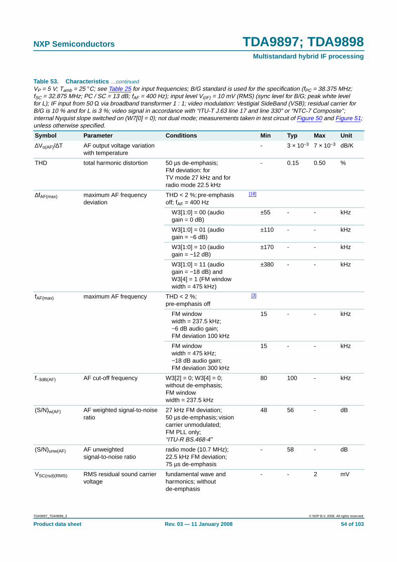
NXP Semiconductors TDA9897; TDA9898Multistandard hybrid IF processing
∆Vo(AF)/∆T AF output voltage variationwith temperature
- 3 × 10⁻³ 7 × 10⁻³ dB/K
THD total harmonic distortion 50 µs de-emphasis;FM deviation: forTV mode 27 kHz and forradio mode 22.5 kHz
- 0.15 0.50 %
∆fAF(max) maximum AF frequencydeviation
THD < 2 %; pre-emphasisoff; fAF = 400 Hz
[18]
W3[1:0] = 00 (audiogain = 0 dB)
±55 - - kHz
W3[1:0] = 01 (audiogain = −6 dB)
±110 - - kHz
W3[1:0] = 10 (audiogain = −12 dB)
±170 - - kHz
W3[1:0] = 11 (audiogain = −18 dB) andW3[4] = 1 (FM windowwidth = 475 kHz)
±380 - - kHz
fAF(max) maximum AF frequency THD < 2 %;pre-emphasis off
[3]
FM windowwidth = 237.5 kHz;−6 dB audio gain;FM deviation 100 kHz
15 - - kHz
FM windowwidth = 475 kHz;−18 dB audio gain;FM deviation 300 kHz
15 - - kHz
f−3dB(AF) AF cut-off frequency W3[2] = 0; W3[4] = 0;without de-emphasis;FM windowwidth = 237.5 kHz
80 100 - kHz
(S/N)w(AF) AF weighted signal-to-noiseratio
27 kHz FM deviation;50 µs de-emphasis; visioncarrier unmodulated;FM PLL only;“ITU-R BS.468-4”
48 56 - dB
(S/N)unw(AF) AF unweightedsignal-to-noise ratio
radio mode (10.7 MHz);22.5 kHz FM deviation;75 µs de-emphasis
- 58 - dB
VSC(rsd)(RMS) RMS residual sound carriervoltage
fundamental wave andharmonics; withoutde-emphasis
- - 2 mV
Table 53. Characteristics …continuedVP = 5 V; Tamb = 25 °C; see Table 25 for input frequencies; B/G standard is used for the specification (fPC = 38.375 MHz;fSC = 32.875 MHz; PC / SC = 13 dB; fAF = 400 Hz); input level Vi(IF) = 10 mV (RMS) (sync level for B/G; peak white levelfor L); IF input from 50 Ω via broadband transformer 1 : 1; video modulation: Vestigial SideBand (VSB); residual carrier forB/G is 10 % and for L is 3 %; video signal in accordance with “ITU-T J.63 line 17 and line 330” or “NTC-7 Composite”;internal Nyquist slope switched on (W7[0] = 0); not dual mode; measurements taken in test circuit of Figure 50 and Figure 51;unless otherwise specified.
Symbol Parameter Conditions Min Typ Max Unit
TDA9897_TDA9898_3 © NXP B.V. 2008. All rights reserved.
Product data sheet Rev. 03 — 11 January 2008 54 of 103

NXP Semiconductors TDA9897; TDA9898Multistandard hybrid IF processing
αAM AM suppression referenced to 27 kHzFM deviation;50 µs de-emphasis;AM: f = 1 kHz; m = 54 %
35 46 - dB
PSRR power supply ripple rejection fripple = 70 Hz;see Figure 11
14 20 - dB
Audio amplifier
Audio output; pin AUD
RO output resistance [3] - - 300 Ω
VO output voltage 2.0 2.4 2.7 V
RL load resistance AC-coupled [3] 10 - - kΩ
DC-coupled [3] 100 - - kΩ
CL load capacitance [3] - - 1 nF
Vo(AF)(RMS) RMS AF output voltage 25 kHz FM deviation;75 µs de-emphasis;see Table 28
0 dB 400 500 600 mV
−6 dB - 250 - mV
−12 dB - 125 - mV
−18 dB - 62.5 - mV
AM; m = 54 %;see Table 28
0 dB 400 500 600 mV
−6 dB - 250 - mV
f−3dB(AF)u upper AF cut-off frequency W3[2] = 0 (withoutde-emphasis)
[19] - 150 - kHz
f−3dB(AF)l lower AF cut-off frequency W3[2] = 0 (withoutde-emphasis)
[20] - 20 - Hz
αmute mute attenuation of AF signal 70 - - dB
∆Vjmp jump voltage difference (DC) switching AF output tomute state or vice versa;activated by digitalacquisition help W3[6] = 1or via W3[5]
- ±50 ±150 mV
PSRR power supply ripple rejection fripple = 70 Hz;see Figure 11
14 20 - dB
De-emphasis network; pin CDEEM
VO output voltage - 2.4 - V
Table 53. Characteristics …continuedVP = 5 V; Tamb = 25 °C; see Table 25 for input frequencies; B/G standard is used for the specification (fPC = 38.375 MHz;fSC = 32.875 MHz; PC / SC = 13 dB; fAF = 400 Hz); input level Vi(IF) = 10 mV (RMS) (sync level for B/G; peak white levelfor L); IF input from 50 Ω via broadband transformer 1 : 1; video modulation: Vestigial SideBand (VSB); residual carrier forB/G is 10 % and for L is 3 %; video signal in accordance with “ITU-T J.63 line 17 and line 330” or “NTC-7 Composite”;internal Nyquist slope switched on (W7[0] = 0); not dual mode; measurements taken in test circuit of Figure 50 and Figure 51;unless otherwise specified.
Symbol Parameter Conditions Min Typ Max Unit
TDA9897_TDA9898_3 © NXP B.V. 2008. All rights reserved.
Product data sheet Rev. 03 — 11 January 2008 55 of 103

NXP Semiconductors TDA9897; TDA9898Multistandard hybrid IF processing
RO output resistance W3[3:2] = 11 (50 µsde-emphasis)
8.5 - 14 kΩ
W3[3:2] = 01 (75 µsde-emphasis)
13 - 21 kΩ
VAF(RMS) RMS AF voltage fAF = 400 Hz;Vo(AF) = 500 mV (RMS);0 dB attenuation
- 170 - mV
AF decoupling
Pin CAF1
Vdec decoupling voltage (DC) fFMPLL = 4.5 MHz 1.5 1.9 3.3 V
fFMPLL = 5.5 MHz 1.5 2.2 3.3 V
fFMPLL = 6.0 MHz 1.5 2.35 3.3 V
fFMPLL = 6.5 MHz 1.5 2.5 3.3 V
fFMPLL = 10.7 MHz 1.5 2.4 3.3 V
IL leakage current ∆VAUD < ±50 mV (p-p);0 dB attenuation
- - ±25 nA
Io(max) maximum output current sink or source 1.15 1.5 1.85 µA
Pin CAF2
VO output voltage - 2.4 - V
FM operation [21] [22]
Single reference QSS AF performance; pin AUD[23]
(S/N)w(SC1) first sound carrier weightedsignal-to-noise ratio
PC / SC1 > 40 dB atpins IF1A and IF1B orIF2A and IF2B;27 kHz FM deviation;BP off; “ITU-R BS.468-4”
black picture 45 50 - dB
white picture 45 50 - dB
6 kHz sine wave(black-to-whitemodulation)
43 47 - dB
250 kHz square wave(black-to-whitemodulation)
45 50 - dB
Table 53. Characteristics …continuedVP = 5 V; Tamb = 25 °C; see Table 25 for input frequencies; B/G standard is used for the specification (fPC = 38.375 MHz;fSC = 32.875 MHz; PC / SC = 13 dB; fAF = 400 Hz); input level Vi(IF) = 10 mV (RMS) (sync level for B/G; peak white levelfor L); IF input from 50 Ω via broadband transformer 1 : 1; video modulation: Vestigial SideBand (VSB); residual carrier forB/G is 10 % and for L is 3 %; video signal in accordance with “ITU-T J.63 line 17 and line 330” or “NTC-7 Composite”;internal Nyquist slope switched on (W7[0] = 0); not dual mode; measurements taken in test circuit of Figure 50 and Figure 51;unless otherwise specified.
Symbol Parameter Conditions Min Typ Max Unit
TDA9897_TDA9898_3 © NXP B.V. 2008. All rights reserved.
Product data sheet Rev. 03 — 11 January 2008 56 of 103

NXP Semiconductors TDA9897; TDA9898Multistandard hybrid IF processing
Single reference QSS AF performance with external FM demodulator connected to OUT1A and OUT1B[24]
(S/N)w(SC1) first sound carrier weightedsignal-to-noise ratio
PC / SC1 > 40 dB atpins IF1A and IF1B orIF2A and IF2B;27 kHz FM deviation;BP off; “ITU-R BS.468-4”
black picture 53 58 - dB
white picture 50 53 - dB
6 kHz sine wave(black-to-whitemodulation)
44 48 - dB
250 kHz square wave(black-to-whitemodulation)
40 45 - dB
sound carriersubharmonics;f = 2.75 MHz ± 3 kHz
45 51 - dB
sound carriersubharmonics;f = 2.87 MHz ± 3 kHz
46 52 - dB
(S/N)w(SC2) second sound carrierweighted signal-to-noise ratio
with external referenceFM demodulator;PC / SC2 > 40 dB atpins IF1A and IF1B orIF2A and IF2B; 27 kHz(54 % FM deviation);BP off; “ITU-R BS.468-4”
black picture 48 55 - dB
white picture 46 51 - dB
6 kHz sine wave(black-to-whitemodulation)
42 46 - dB
250 kHz square wave(black-to-whitemodulation)
29 34 - dB
sound carriersubharmonics;f = 2.75 MHz ± 3 kHz
44 50 - dB
sound carriersubharmonics;f = 2.87 MHz ± 3 kHz
45 51 - dB
Table 53. Characteristics …continuedVP = 5 V; Tamb = 25 °C; see Table 25 for input frequencies; B/G standard is used for the specification (fPC = 38.375 MHz;fSC = 32.875 MHz; PC / SC = 13 dB; fAF = 400 Hz); input level Vi(IF) = 10 mV (RMS) (sync level for B/G; peak white levelfor L); IF input from 50 Ω via broadband transformer 1 : 1; video modulation: Vestigial SideBand (VSB); residual carrier forB/G is 10 % and for L is 3 %; video signal in accordance with “ITU-T J.63 line 17 and line 330” or “NTC-7 Composite”;internal Nyquist slope switched on (W7[0] = 0); not dual mode; measurements taken in test circuit of Figure 50 and Figure 51;unless otherwise specified.
Symbol Parameter Conditions Min Typ Max Unit
TDA9897_TDA9898_3 © NXP B.V. 2008. All rights reserved.
Product data sheet Rev. 03 — 11 January 2008 57 of 103

NXP Semiconductors TDA9897; TDA9898Multistandard hybrid IF processing
AM operation
L standard; pin AUD
Vo(AF)(RMS) RMS AF output voltage 54 % modulation 400 500 600 mV
THD total harmonic distortion 54 % modulation; BP on;see Figure 33
- 0.5 1.0 %
BAF(−3dB) −3 dB AF bandwidth 12 18 - kHz
(S/N)w(AF) AF weighted signal-to-noiseratio
“ITU-R BS.468-4”
BP on 38 42 - dB
BP off 44 50 - dB
composite IF; VIFmodulation = color bar;“ITU-R BS.468-4”; BP on
[3] - 40 - dB
Reference frequency
General
fref reference frequency [25] - 4 - MHz
Reference frequency generation with crystal; pin OPTXTAL
VOPTXTAL voltage on pin OPTXTAL(DC)
pin open-circuit 2.3 2.6 2.9 V
Ri input resistance [3] - 2 - kΩ
Rrsn(xtal) crystal resonance resistance - - 200 Ω
Cpull pull capacitance [26] - - - pF
Rswoff(OPTXTAL) switch-off resistance on pinOPTXTAL
to switch off crystal inputby external resistor wiredbetween pin OPTXTALand GND
0.22 - 4.7 kΩ
Iswoff switch-off current Rswoff(OPTXTAL) = 0.22 kΩ - - 1600 µA
Rswoff(OPTXTAL) = 3.3 kΩ - 500 - µA
Reference frequency input from external source; pin OPTXTAL
VOPTXTAL voltage on pin OPTXTAL(DC)
pin open-circuit 2.3 2.6 2.9 V
Ri input resistance [3] - 2 - kΩ
Vref(RMS) RMS reference voltage 80 - 400 mV
RO output resistance of external referencesignal source
[3] - 2 4.7 kΩ
Cdec decoupling capacitance to external referencesignal source
[3] 22 100 - pF
Reference frequency input from external source; W7[7] = 0; pin FREF
VFREF voltage on pin FREF (DC) pin open-circuit 2.2 2.5 2.8 V
Ri input resistance [3] 50 - - kΩ
Table 53. Characteristics …continuedVP = 5 V; Tamb = 25 °C; see Table 25 for input frequencies; B/G standard is used for the specification (fPC = 38.375 MHz;fSC = 32.875 MHz; PC / SC = 13 dB; fAF = 400 Hz); input level Vi(IF) = 10 mV (RMS) (sync level for B/G; peak white levelfor L); IF input from 50 Ω via broadband transformer 1 : 1; video modulation: Vestigial SideBand (VSB); residual carrier forB/G is 10 % and for L is 3 %; video signal in accordance with “ITU-T J.63 line 17 and line 330” or “NTC-7 Composite”;internal Nyquist slope switched on (W7[0] = 0); not dual mode; measurements taken in test circuit of Figure 50 and Figure 51;unless otherwise specified.
Symbol Parameter Conditions Min Typ Max Unit
TDA9897_TDA9898_3 © NXP B.V. 2008. All rights reserved.
Product data sheet Rev. 03 — 11 January 2008 58 of 103

NXP Semiconductors TDA9897; TDA9898Multistandard hybrid IF processing
fref reference frequency [25] - 4 - MHz
Vref(RMS) RMS reference voltage see Figure 34 15 150 500 mV
RO output resistance of external referencesignal source;AC-coupled
- - 4.7 kΩ
Cdec decoupling capacitance to external referencesignal source
22 100 - pF
Rswoff(FREF) switch-off resistance onpin FREF
to switch off referencesignal input by externalresistor wired betweenpin FREF and GND
3.9 - 27 kΩ
Iswoff switch-off current Rswoff(FREF) = 3.9 kΩ - - 100 µA
Rswoff(FREF) = 22 kΩ - 75 - µA
I2C-bus transceiver [27]
Address select; pin ADRSEL
VADRSEL voltage on pin ADRSEL (DC) pin open-circuit - 0.5VP - V
for address select
MAD1; pin connectedto GND
0 - 0.04VP V
MAD3; pin connectedto GND via RADRSEL
0.12VP - 0.30VP V
MAD4; pin connectedto VP via RADRSEL
0.66VP - 0.86VP V
MAD2; pin connectedto VP
0.96VP - VP V
Ri input resistance [3] - 35 - kΩ
RADRSEL resistance on pin ADRSEL 42.3 47 51.7 kΩ
I2C-bus voltage select; pin BVS
VBVS voltage on pin BVS (DC) pin open-circuit - 0.52VP - V
Isink(I) input sink current pin connected to VP - - 10 µA
Isource(I) input source current pin connected to GND - - 60 µA
VI input voltage VCC(I2C-bus) = 5.0 V; pinconnected to VP
0.88VP - VP V
VCC(I2C-bus) = 3.3 V; pinopen-circuit
0.46VP - 0.58VP V
VCC(I2C-bus) = 2.5 V; pinconnected to GND
0 - 0.12VP V
Table 53. Characteristics …continuedVP = 5 V; Tamb = 25 °C; see Table 25 for input frequencies; B/G standard is used for the specification (fPC = 38.375 MHz;fSC = 32.875 MHz; PC / SC = 13 dB; fAF = 400 Hz); input level Vi(IF) = 10 mV (RMS) (sync level for B/G; peak white levelfor L); IF input from 50 Ω via broadband transformer 1 : 1; video modulation: Vestigial SideBand (VSB); residual carrier forB/G is 10 % and for L is 3 %; video signal in accordance with “ITU-T J.63 line 17 and line 330” or “NTC-7 Composite”;internal Nyquist slope switched on (W7[0] = 0); not dual mode; measurements taken in test circuit of Figure 50 and Figure 51;unless otherwise specified.
Symbol Parameter Conditions Min Typ Max Unit
TDA9897_TDA9898_3 © NXP B.V. 2008. All rights reserved.
Product data sheet Rev. 03 — 11 January 2008 59 of 103

NXP Semiconductors TDA9897; TDA9898Multistandard hybrid IF processing
[1] Values of video and sound parameters can be decreased at VP = 4.5 V.
[2] Condition for secure POR is a rise or fall time greater than 2 µs.
[3] This parameter is not tested during the production and is only given as application information for designing the receiver circuit.
[4] Level headroom for input level jumps during gain control setting.
[5] BLF(−3dB) = 100 kHz (damping factor d = 1.9; calculated with sync level within gain control range). Calculation of the VIF PLL filter can bedone by use of the following formula:
, valid for d ≥ 1.2
,
where:
KO is the VCO steepness or ; KD is the phase detector steepness ;
R is the loop filter serial resistor (Ω); C is the loop filter serial capacitor (F); BLF(−3dB) is the −3 dB LF bandwidth (Hz); d is the dampingfactor.
[6] The VCO frequency offset related to the PC frequency is set to 1 MHz with white picture video modulation.
[7] AC load; CL < 20 pF and RL > 1 kΩ. The sound carrier frequencies (depending on TV standard) are attenuated by the integrated soundcarrier traps.
[8] Condition: luminance range (5 steps) from 0 % to 100 %. Measurement value is based on 4 of 5 steps.
[9] Measurement using 200 kHz high-pass filter, 5 MHz low-pass filter and subcarrier notch filter (“ITU-T J.64”).
[10] Modulation VSB; sound carrier off; fvideo > 0.5 MHz.
[11] Sound carrier on; fvideo = 10 kHz to 10 MHz.
[12] The sound carrier trap can be bypassed by setting the I2C-bus bit W2[0] to logic 0; see Table 24. In this way the full composite videospectrum appears at pin CVBS. The video amplitude is reduced to 1.1 V (p-p).
[13] Measurement condition: with transformer, transmitter pre-correction on; reference is at 1 MHz.
[14] The response time is valid for a VIF input level range from 200 µV to 70 mV.
[15] See Figure 19 to smooth current pulses.
I2C-bus transceiver; pins SCL and SDA[28]
VIH HIGH-level input voltage VCC(I2C-bus) = 5.0 V [29] 0.6VP - VP V
VCC(I2C-bus) = 3.3 V [30] 2.3 - VP V
VCC(I2C-bus) = 2.5 V [30] 1.75 - VP V
VIL LOW-level input voltage VCC(I2C-bus) = 5.0 V [29] −0.3 - +0.3VP V
VCC(I2C-bus) = 3.3 V [30] −0.3 - +1.0 V
VCC(I2C-bus) = 2.5 V [30] −0.3 - +0.75 V
IIH HIGH-level input current −10 - +10 µA
IIL LOW-level input current −10 - +10 µA
VOL LOW-level output voltage IOL = 3 mA; for datatransmission (SDA)
- - 0.4 V
fSCL SCL clock frequency 0 - 400 kHz
Table 53. Characteristics …continuedVP = 5 V; Tamb = 25 °C; see Table 25 for input frequencies; B/G standard is used for the specification (fPC = 38.375 MHz;fSC = 32.875 MHz; PC / SC = 13 dB; fAF = 400 Hz); input level Vi(IF) = 10 mV (RMS) (sync level for B/G; peak white levelfor L); IF input from 50 Ω via broadband transformer 1 : 1; video modulation: Vestigial SideBand (VSB); residual carrier forB/G is 10 % and for L is 3 %; video signal in accordance with “ITU-T J.63 line 17 and line 330” or “NTC-7 Composite”;internal Nyquist slope switched on (W7[0] = 0); not dual mode; measurements taken in test circuit of Figure 50 and Figure 51;unless otherwise specified.
Symbol Parameter Conditions Min Typ Max Unit
BLF 3dB–( )1
2π------KOKDR=
d12---R KOKDC=
radsV--------
2πHzV------
Arad--------
TDA9897_TDA9898_3 © NXP B.V. 2008. All rights reserved.
Product data sheet Rev. 03 — 11 January 2008 60 of 103

NXP Semiconductors TDA9897; TDA9898Multistandard hybrid IF processing
[16] To match the AFC output signal to different tuning systems a current output is provided. The test circuit is given in Figure 19. TheAFC steepness can be changed by resistors R1 and R2.
[17] The AFC value of the VIF and RIF frequency is generated by using digital counting methods. The used counter resolution is providedwith an uncertainty of ±1 bit corresponding to ±25 kHz. This uncertainty of ±25 kHz has to be added to the frequency accuracyparameter.
[18] Measured with an FM deviation of 25 kHz and the typical AF output voltage of 500 mV (RMS). The audio signal processing stageprovides headroom of 6 dB with THD < 1.5 %. The I2C-bus bits W3[0] and W3[1] control the AF output signal amplitude from0 dB to −18 dB in steps of −6 dB. Reducing the audio gain for handling a frequency deviation of more than 55 kHz avoids AF outputsignal clipping.
[19] Amplitude response depends on dimensioning of FM PLL loop filter.
[20] The lower AF cut-off frequency depends on the value of the capacitor at pin CAF1. A value of CAF1 = 470 nF leads to f−3dB(AF)l ≈ 20 Hzand CAF1 = 220 nF leads to f−3dB(AF)l ≈ 40 Hz.
[21] For all signal-to-noise measurements the used VIF modulator has to meet the following specifications:
a) Incidental phase modulation for black-to-white jump less than 0.5 degrees.
b) QSS AF performance, measured with the television demodulator AMF2 (audio output, weighted signal-to-noise ratio) better than60 dB (at deviation 27 kHz) for 6 kHz sine wave black-to-white video modulation.
c) Picture-to-sound carrier ratio PC / SC1 = 13 dB (transmitter).
[22] The PC / SC ratio is calculated as the addition of TV transmitter PC / SC1 ratio and SAW filter PC / SC1 ratio. This PC / SC ratio isnecessary to achieve the weighted signal-to-noise values as noted. A different PC / SC ratio will change these values.
[23] Measurement condition is SC1 / SC2 ≥ 7 dB.
[24] The differential QSS signal output on pins OUT1A and OUT1B is analyzed by a test demodulator TDA9820. The signal-to-noise ratio ofthis device is better than 60 dB. The measurement is related to an FM deviation of ±27 kHz and in accordance with “ITU-R BS.468-4”.
[25] The tolerance of the reference frequency determines the accuracy of VIF AFC, RIF AFC, FM demodulator center frequency, maximumFM deviation, sound trap frequency, LIF band-pass cut-off frequency and ZIF low-pass cut-off frequency as well as the accuracy of thesynthesizer.
[26] The value of Cpull determines the accuracy of the resonance frequency of the crystal. It depends on the used type of crystal.
[27] The AC characteristics are in accordance with the I2C-bus specification for fast mode (maximum clock frequency is 400 kHz).Information about the I2C-bus can be found in the brochure “The I2C-bus and how to use it” (order number 9398 393 40011).
[28] The SDA and SCL lines will not be pulled down if VP is switched off.
[29] The threshold is dependent on VP.
[30] The threshold is independent of VP.
Table 54. Examples to the FM PLL filter
BLF(−3dB) (kHz) Cs (nF) Cpar (pF) Rs (kΩ) Comment
210 2.2 100 8.2 recommended for single-carrier-sound,FM narrow
410 2.2 47 5.6 recommended for single-carrier-sound, FM wide
130 2.2 470 5.6 recommended for two-carrier-sound, FM narrow
210 2.2 47 8.2 used for test circuit
Table 55. Input frequencies and carrier ratios (examples)
Symbol Parameter B/G standard M/N standard L standard L-accent standard Unit
fPC picture carrier frequency 38.375 38.375 38.375 33.625 MHz
fSC1 sound carrier frequency 1 32.825 33.825 31.825 40.125 MHz
fSC2 sound carrier frequency 2 32.583 - - - MHz
PC / SC1 picture to first sound carrier ratio 13 7 10 10 dB
PC / SC2 picture to second sound carrier ratio 20 - - - dB
TDA9897_TDA9898_3 © NXP B.V. 2008. All rights reserved.
Product data sheet Rev. 03 — 11 January 2008 61 of 103

NXP Semiconductors TDA9897; TDA9898Multistandard hybrid IF processing
Fig 10. Typical video signal levels on output pin CVBS (sound carrier off)
Fig 11. Ripple rejection condition
1.20 V
1.80 V
3.20 V white level3.41 V
1.5 V
2.72 V2.6 V
1.83 V
zero carrier level
black level
sync level
mhc115
trap bypass mode
normal mode
001aae391
TDA9897TDA9898
V = VP + Vripple
VP (V)
5.050
5.000
4.950
t (s)
TDA9897_TDA9898_3 © NXP B.V. 2008. All rights reserved.
Product data sheet Rev. 03 — 11 January 2008 62 of 103

NXP Semiconductors TDA9897; TDA9898Multistandard hybrid IF processing
(1) VIF AGC.
(2) TAGC; W10 = 00h.
(3) TAGC; W10 = 10h.
(4) TAGC; W10 = 1Fh.
Fig 12. Typical VIF monitor and TAGC characteristic
Fig 13. Typical tuner takeover point as a function of I 2C-bus register W9 or W10
001aad353
Vi(VIF) (dBµV)30 13011070 9050
2
3
1
4
5
VTAGC(V)
0
(1) (2) (3) (4)2
3
1
4
5
Vmonitor(VIFAGC)(V)
0
bit pattern W9[4:0] or W10[4:0]
0 0 0 0 0 0 0 0 0 0 0 0 0 0 0 0 1 1 1 1 1 1 1 1 1 1 1 1 1 1 1 1
0 1 0 1 0 1 0 1 0 1 0 1 0 1 0 1 0 1 0 1 0 1 0 1 0 1 0 1 0 1 0 1
0 0 1 1 0 0 1 1 0 0 1 1 0 0 1 1 0 0 1 1 0 0 1 1 0 0 1 1 0 0 1 1
0 0 0 0 1 1 1 1 0 0 0 0 1 1 1 1 0 0 0 0 1 1 1 1 0 0 0 0 1 1 1 1
0 0 0 0 0 0 0 0 1 1 1 1 1 1 1 1 0 0 0 0 0 0 0 0 1 1 1 1 1 1 1 1
001aaf640
70
80
60
90
100
Vi(IF)(dBµV)
50
Integral TAGC (W9); step width: 1.3 dBµV.IF based TAGC (W10).
TDA9897_TDA9898_3 © NXP B.V. 2008. All rights reserved.
Product data sheet Rev. 03 — 11 January 2008 63 of 103

NXP Semiconductors TDA9897; TDA9898Multistandard hybrid IF processing
(1) IF based TAGC (TOP2).
Fig 14. Typical tuner takeover point as a function of resistor R TOP2
008aaa034
RTOP2 (kΩ)0 252010 155
80
70
90
100
Vi(IF)(dBµV)
60
(1)
(1) AM.
(2) FM.
Fig 15. Typical FM AGC characteristic measured atpin MPP2
Fig 16. Typical SIF AGC characteristic measured atpin MPP2
001aad356
Vi(EXTFMI) (dBµV)40 12010060 80
2
3
1
4
5
VAGC(FM)(V)
0
001aad357
Vi(SIF) (dBµV)20 12010060 8040
2
3
1
4
5
VAGC(SIF)(V)
0
(1) (2)
TDA9897_TDA9898_3 © NXP B.V. 2008. All rights reserved.
Product data sheet Rev. 03 — 11 January 2008 64 of 103

NXP Semiconductors TDA9897; TDA9898Multistandard hybrid IF processing
(1) VIF AFC via I2C-bus; accuracy is ±1 digit.
(2) Bit AFCWIN via I2C-bus (VCO is in ±1.6 MHz window) for all standards except M/N standard.
(3) Bit AFCWIN via I2C-bus (VCO is in ±0.8 MHz window) for M/N standard.
(4) VIF AFC average current.
(5) Reading via I2C-bus.
(6) Average; RC network at pin MPP2.
Fig 17. Typical analog and digital AFC characteristic for VIF
008aaa035
0
−50
50
−150
150
250
−250
0
−50
50
−150
150
250
IAFC(6)
(µA)
−250
fVIF (MHz)36.375 40.37539.87537.875 38.87537.37536.875 38.375 39.375
bit AFCWIN (R1[7]) = 1
(1)
(4)
(2)
(3)
∆fAFC(VIF)(5)
(kHz)
Characteristics of digital and analog radio AFC is mirrored with respect to center frequency when lower sideband is used(W2[3] = 0).
(1) RIF AFC via I2C-bus.
(2) FM carrier detection via I2C-bus.
(3) RIF AFC average current.
(4) Reading via I2C-bus.
(5) Average; RC network at pin MPP2.
Fig 18. Typical analog and digital AFC characteristic for RIF
001aad443
0 0
−50
50
−150
150
250
IAFC(5)
(µA)
−250
fRIF (MHz)5.0 6.05.85.4 5.65.2
AFC undefinedAFC undefined bit CARRDET (R1[5]) = 1
(1)
(3)
(2)
−50
50
−150
150
250
∆fAFC(RIF)(4)
(kHz)
−250
TDA9897_TDA9898_3 © NXP B.V. 2008. All rights reserved.
Product data sheet Rev. 03 — 11 January 2008 65 of 103

NXP Semiconductors TDA9897; TDA9898Multistandard hybrid IF processing
Fig 19. RC network for measurement of analog AFC characteristic
(1) B/G standard; weighted video S/N; using 50 % grey picture.
(2) M/N standard; unweighted video S/N; using 50 IRE grey picture.
Fig 20. Typical signal-to-noise ratio as a function of VIF input voltage
001aae392
100 nFR222 kΩ
R122 kΩ
MPP2IAFC
VP
TDA9897TDA9898
Vi(VIF) (dBµV)50 1009070 8060
001aad660
40
50
60
S/N(dB)
30
(1)
(2)
TDA9897_TDA9898_3 © NXP B.V. 2008. All rights reserved.
Product data sheet Rev. 03 — 11 January 2008 66 of 103

NXP Semiconductors TDA9897; TDA9898Multistandard hybrid IF processing
(1) Minimum requirements upper limit.
(2) Minimum requirements lower limit.
(3) Typical trap amplitude frequency response.
Fig 21. Typical amplitude frequency response for sound trap at M/N standard (includingKorea)
(1) Minimum requirements upper limit.
(2) Minimum requirements lower limit.
(3) Typical trap group delay response.
Fig 22. Typical group delay response for sound trap at M/N standard
001aad487
f (MHz)0 1 3 5 642
−25
−15
−35
−5
−10
5
0αresp(f)
(dB)
−45
−20
−30
−40
(1)
(2) (3)
f (MHz)0 621 4 53
001aad365
td(grp)(ns)
−50
−100
50
0
−150
−200
150
100
250
200
−250
(1)
(3)
(2)
TDA9897_TDA9898_3 © NXP B.V. 2008. All rights reserved.
Product data sheet Rev. 03 — 11 January 2008 67 of 103

NXP Semiconductors TDA9897; TDA9898Multistandard hybrid IF processing
(1) Minimum requirements upper limit.
(2) Minimum requirements lower limit.
(3) Typical trap amplitude frequency response.
Fig 23. Typical amplitude frequency response for sound trap at B/G standard
(1) Minimum requirements upper limit.
(2) Minimum requirements lower limit.
(3) Typical trap group delay response.
Fig 24. Typical group delay response for sound trap at B/G standard
001aad488
f (MHz)0 8642 7531
−25
−15
−35
−5
5
0αresp(f)
(dB)
−45
−20
−10
−30
−40
(1)
(2) (3)
f (MHz)0 87621 4 53
001aad361
td(grp)(ns)
0
−50
−100
50
−150
−200
150
100
250
200
−250
(1)
(3)
(2)
TDA9897_TDA9898_3 © NXP B.V. 2008. All rights reserved.
Product data sheet Rev. 03 — 11 January 2008 68 of 103

NXP Semiconductors TDA9897; TDA9898Multistandard hybrid IF processing
(1) Minimum requirements upper limit.
(2) Minimum requirements lower limit.
(3) Typical trap amplitude frequency response.
Fig 25. Typical amplitude frequency response for sound trap at I standard
(1) Minimum requirements upper limit.
(2) Minimum requirements lower limit.
(3) Typical trap group delay response.
Fig 26. Typical group delay response for sound trap at I standard
001aad489
f (MHz)0 86421 753
−25
−15
−35
−5
5
0αresp(f)
(dB)
−45
−20
−10
−30
−40
(1)
(2) (3)
f (MHz)0 87621 4 53
001aad363
td(grp)(ns)
−50
−100
50
0
−150
−200
150
100
250
200
−250
(1)
(3)
(2)
TDA9897_TDA9898_3 © NXP B.V. 2008. All rights reserved.
Product data sheet Rev. 03 — 11 January 2008 69 of 103

NXP Semiconductors TDA9897; TDA9898Multistandard hybrid IF processing
(1) Minimum requirements upper limit.
(2) Minimum requirements lower limit.
(3) Typical trap amplitude frequency response.
Fig 27. Typical amplitude frequency response for sound trap at D/K standard
(1) Minimum requirements upper limit.
(2) Minimum requirements lower limit.
(3) Typical trap group delay response.
Fig 28. Typical group delay response for sound trap at D/K standard
001aaf551
f (MHz)0 86421 753
−25
−15
−35
−5
5
0αresp(f)
(dB)
−45
−20
−10
−30
−40
(1)
(2)
(3)
001aaf552
f (MHz)0 87621 4 53
td(grp)(ns)
−50
−100
50
0
−150
−200
150
100
250
200
−250
(1)
(3)
(2)
TDA9897_TDA9898_3 © NXP B.V. 2008. All rights reserved.
Product data sheet Rev. 03 — 11 January 2008 70 of 103

NXP Semiconductors TDA9897; TDA9898Multistandard hybrid IF processing
(1) Minimum requirements upper limit.
(2) Minimum requirements lower limit.
(3) Typical trap amplitude frequency response.
Fig 29. Typical amplitude frequency response for sound trap at L standard
(1) Minimum requirements upper limit.
(2) Minimum requirements lower limit.
(3) Typical trap group delay response.
Fig 30. Typical group delay response for sound trap at L standard
001aad491
f (MHz)0 86421 753
−25
−15
−35
−5
5
0αresp(f)
(dB)
−45
−20
−10
−30
−40
(1)
(2) (3)
f (MHz)0 87621 4 53
001aad364
td(grp)(ns)
0
−50
−100
50
−150
−200
150
100
250
200
−250
(1)
(3)
(2)
TDA9897_TDA9898_3 © NXP B.V. 2008. All rights reserved.
Product data sheet Rev. 03 — 11 January 2008 71 of 103

NXP Semiconductors TDA9897; TDA9898Multistandard hybrid IF processing
(1) Center frequency.
(2) Minimum upper cut-off frequency.
(3) Minimum lower cut-off frequency.
(4) Maximum upper cut-off frequency.
(5) Maximum lower cut-off frequency.
(6) Minimum upper stop-band attenuation.
(7) Minimum lower stop-band attenuation.
Fig 31. Typical sound BP amplitude frequency response at TV mode, normalized to BPcenter frequency
f − fc (MHz)−3.0 3.01.0−1.0 2.00−2.0
001aaf579
−30
−10
−20
−40
10
0
αresp(f)(dB)
−50
(7)
(5)
(3) (2)
(1)
(4)
(6)
TDA9897_TDA9898_3 © NXP B.V. 2008. All rights reserved.
Product data sheet Rev. 03 — 11 January 2008 72 of 103

NXP Semiconductors TDA9897; TDA9898Multistandard hybrid IF processing
(1) Center frequency.
(2) Minimum upper cut-off frequency.
(3) Minimum lower cut-off frequency.
(4) Maximum upper cut-off frequency.
(5) Maximum lower cut-off frequency.
(6) Minimum upper stop-band attenuation.
(7) Minimum lower stop-band attenuation.
Fig 32. Typical sound BP amplitude frequency response at radio 10.7 mode, normalized toBP center frequency
Fig 33. Typical total harmonic distortion as a function of audio frequency at AM standard
f − fc (MHz)−3.0 3.01.0−1.0 2.00−2.0
001aaf578
−30
−10
−20
−40
10
0
αresp(f)(dB)
−50
(7)
(5)
(3) (2)
(1)
(4)
(6)
001aad359
fAF (kHz)10−2 1021010−1 1
1.0
0.5
1.5
2.0
THD(%)
0
TDA9897_TDA9898_3 © NXP B.V. 2008. All rights reserved.
Product data sheet Rev. 03 — 11 January 2008 73 of 103

NXP Semiconductors TDA9897; TDA9898Multistandard hybrid IF processing
Reference frequency input signal taken from external quartz circuit.
Fig 34. Weighted FM audio S/N versus reference frequency input level using radio mode
001aaf468
Vi(FREF)(RMS) (mV)0 20015050 100
35
45
55
(S/N)w(dB)
25
TDA9897_TDA9898_3 © NXP B.V. 2008. All rights reserved.
Product data sheet Rev. 03 — 11 January 2008 74 of 103
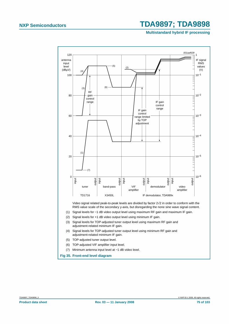
NXP Semiconductors TDA9897; TDA9898Multistandard hybrid IF processing
Video signal related peak-to-peak levels are divided by factor 2√2 in order to conform with theRMS value scale of the secondary y-axis, but disregarding the none sine wave signal content.
(1) Signal levels for −1 dB video output level using maximum RF gain and maximum IF gain.
(2) Signal levels for +1 dB video output level using minimum IF gain.
(3) Signal levels for TOP-adjusted tuner output level using maximum RF gain andadjustment-related minimum IF gain.
(4) Signal levels for TOP-adjusted tuner output level using minimum RF gain andadjustment-related minimum IF gain.
(5) TOP-adjusted tuner output level.
(6) TOP-adjusted VIF amplifier input level.
(7) Minimum antenna input level at −1 dB video level.
Fig 35. Front-end level diagram
001aaf639120
100
80
60
40
20
0
antennainputlevel
(dBµV)
videoamplifier
demodulatorVIFamplifier
band-passtuner
IF demodulator, TDA989xX3450LTD1716
inpu
t
inpu
t
outp
ut
outp
ut
outp
ut
outp
ut
outp
ut
inpu
t
inpu
t
inpu
t
IF signalRMS
values(V)
1
10−1
10−2
10−3
10−4
10−5
10−6
(7)
(1)
(3)
(4)
(2)(5)
(6)
IF gaincontrolrange
RFgain
controlrange
IF gaincontrol
range limitedby TOP
adjustment
TDA9897_TDA9898_3 © NXP B.V. 2008. All rights reserved.
Product data sheet Rev. 03 — 11 January 2008 75 of 103

NXP Semiconductors TDA9897; TDA9898Multistandard hybrid IF processing
12.2 Digital TV signal processing
Table 56. CharacteristicsVP = 5 V[1]; Tamb = 25 °C; 8 MHz system; see Table 34 and Table 35; CW test input signal is used for specification;Vi(IF) = 10 mV (RMS); fIF = 36 MHz for low IF output of 5 MHz; IF input from 50 Ω via broadband transformer 1 : 1;gain controlled amplifier adjusted to typical specified output level; measurements taken in test circuit ofFigure 50 and Figure 51 with 4 MHz crystal oscillator reference; unless otherwise specified.
Symbol Parameter Conditions Min Typ Max Unit
IF amplifier; pins IF3A and IF3B or IF1A and IF1B or IF2A and IF2B
VI input voltage 1.8 1.93 2.2 V
Ri(dif) differential inputresistance
[2] - 2 - kΩ
Ci(dif) differential inputcapacitance
[2] - 3 - pF
GIF(cr) control range IF gain [2] 60 66 - dB
DTV differential output; pins OUT1A, OUT1B, OUT2A and OUT2B
VO output voltage pin open-circuit 1.8 2.0 2.2 V
Ibias(int) internal bias current(DC)
for emitter-follower 2.0 2.5 - mA
Isink(o)(max) maximum output sinkcurrent
DC and AC; see Figure 36 [3] 1.4 1.7 - mA
Isource(o)(max) maximum outputsource current
DC and AC; see Figure 36 [3] 6.0 - - mA
RO output resistance differential; output active [2] - - 50 Ω
output inactive; internalresistance to GND
[2] - 800 - Ω
Vi(IF)(RMS) RMS IF input voltage minimum input sine wavelevel for nominal output level
- 70 100 µV
maximum input sine wavelevel for nominal output level
130 170 - mV
permissible overload [2] - - 320 mV
Direct IF; pins OUT2A and OUT2B
GIF(max) maximum IF gain output peak-to-peak level toinput RMS level ratio
[2] - 83 - dB
Vo(dif)(p-p) peak-to-peakdifferential outputvoltage
between pin OUT2A andpin OUT2B
[4]
W4[7] = 0 - 1.0 1.1 V
W4[7] = 1 - 0.50 0.55 V
C/N carrier-to-noise ratio at fo = 33.4 MHz;see Figure 37
[2][5][6]
Vi(IF) = 10 mV (RMS) 115 124 - dBc/Hz
Vi(IF) = 0.5 mV (RMS) 90 104 - dBc/Hz
αIM intermodulationsuppression
input signals: fi = 47.0 MHzand 57.5 MHz; outputsignals: fo = 36.5 MHz or68.0 MHz; see Figure 38
[2]
W4[7] = 0 40 - - dB
W4[7] = 1 40 - - dB
TDA9897_TDA9898_3 © NXP B.V. 2008. All rights reserved.
Product data sheet Rev. 03 — 11 January 2008 76 of 103

NXP Semiconductors TDA9897; TDA9898Multistandard hybrid IF processing
fIF(−1dB)l lower −1 dB IF cut-offfrequency
[2] - 7 - MHz
f−3dB(IF)u upper IF cut-offfrequency
W4[7] = 0 [4] 60 - - MHz
W4[7] = 1 [7] 60 - - MHz
PSRR power supply ripplerejection
residual spurious at nominaldifferential output voltagedependent on power supplyripple
[2]
fripple = 70 Hz - 60 - dB
fripple = 20 kHz - 60 - dB
Low or zero IF output signal; pins OUT1A and OUT1B or pins OUT2A and OUT2B; differential
GIF(max) maximum IF gain output peak-to-peak level toinput RMS level ratio
[2] - 89 - dB
fsynth synthesizer frequency see Table 35 and Table 36 - - - MHz
Vo(dif)(p-p) peak-to-peakdifferential outputvoltage
W4[7] = 0 [4] - 2 - V
W4[7] = 1 [4] - 1 - V
PSRR power supply ripplerejection
residual spurious at nominaldifferential output voltagedependent on power supplyripple
[2]
fripple = 70 Hz - 50 - dB
fripple = 20 kHz - 30 - dB
Low IF output signal; pins OUT1A and OUT1B
αripple(pb)LIF low IF pass-bandripple
6 MHz bandwidth - - 2.7 dB
7 MHz bandwidth - - 2.7 dB
8 MHz bandwidth - - 2.7 dB
B−3dB −3 dB bandwidth BP off [4] 11 15 - MHz
6 MHz bandwidth [4] - 7.8 - MHz
7 MHz bandwidth [4] - 8.8 - MHz
8 MHz bandwidth [4] - 9.8 - MHz
αstpb stop-band attenuation 6 MHz band; f = 11.75 MHz 30 40 - dB
6 MHz band; f = 20 MHz 28 35 - dB
7 MHz band; f = 13.75 MHz 30 40 - dB
7 MHz band; f = 20 MHz 28 35 - dB
8 MHz band; f = 15.75 MHz 30 40 - dB
8 MHz band; f = 20 MHz 28 35 - dB
Table 56. Characteristics …continuedVP = 5 V[1]; Tamb = 25 °C; 8 MHz system; see Table 34 and Table 35; CW test input signal is used for specification;Vi(IF) = 10 mV (RMS); fIF = 36 MHz for low IF output of 5 MHz; IF input from 50 Ω via broadband transformer 1 : 1;gain controlled amplifier adjusted to typical specified output level; measurements taken in test circuit ofFigure 50 and Figure 51 with 4 MHz crystal oscillator reference; unless otherwise specified.
Symbol Parameter Conditions Min Typ Max Unit
TDA9897_TDA9898_3 © NXP B.V. 2008. All rights reserved.
Product data sheet Rev. 03 — 11 January 2008 77 of 103

NXP Semiconductors TDA9897; TDA9898Multistandard hybrid IF processing
∆td(grp) group delay timevariation
from 1 MHz to 2 MHz [2] - 90 200 ns
from 2 MHz to end of bandwith a bandwidth of
[2]
6 MHz - 90 160 ns
7 MHz - 90 160 ns
8 MHz - 90 160 ns
αimage image rejection −10 MHz to 0 MHz
BP on 30 34 - dB
BP off 24 28 - dB
C/N carrier-to-noise ratio at fo = 4.9 MHz;see Figure 37
[2][5][6]
Vi(IF) = 10 mV (RMS) 112 118 - dBc/Hz
Vi(IF) = 0.5 mV (RMS) 90 104 - dBc/Hz
αH(ib) in-band harmonicssuppression
low IF = multiple of1.31 MHz;fi = fsynth + 1.31 MHz;see Figure 41
[2]
W4[7] = 0 40 - - dB
W4[7] = 1 40 - - dB
αIM intermodulationsuppression
input signals:fi = fsynth + 4.7 MHz andfsynth + 5.3 MHz; outputsignals: fo = 4.1 MHz or5.9 MHz; see Figure 40
[2]
W4[7] = 0 40 - - dB
W4[7] = 1 40 - - dB
αsp(ib) in-band spurioussuppression
single-ended AC load;RL = 1 kΩ; CL = 5 pF;1 MHz to end of band;BP on
[2] 50 - - dB
αsp(ob) out-band spurioussuppression
single-ended AC load;RL = 1 kΩ; CL = 5 pF; BP on
[2] 50 - - dB
Zero IF output signal; pins OUT1A and OUT1B or pins OUT2A and OUT2B
αripple(pb)ZIF zero IF pass-bandripple
3.0 MHz bandwidth - - 1.8 dB
3.5 MHz bandwidth - - 1.8 dB
4.0 MHz bandwidth - - 1.8 dB
B−3dB −3 dB bandwidth BP off [4] 11 15 - MHz
3.0 MHz bandwidth [4] - 3.7 - MHz
3.5 MHz bandwidth [4] - 4.2 - MHz
4.0 MHz bandwidth [4] - 4.7 - MHz
Table 56. Characteristics …continuedVP = 5 V[1]; Tamb = 25 °C; 8 MHz system; see Table 34 and Table 35; CW test input signal is used for specification;Vi(IF) = 10 mV (RMS); fIF = 36 MHz for low IF output of 5 MHz; IF input from 50 Ω via broadband transformer 1 : 1;gain controlled amplifier adjusted to typical specified output level; measurements taken in test circuit ofFigure 50 and Figure 51 with 4 MHz crystal oscillator reference; unless otherwise specified.
Symbol Parameter Conditions Min Typ Max Unit
TDA9897_TDA9898_3 © NXP B.V. 2008. All rights reserved.
Product data sheet Rev. 03 — 11 January 2008 78 of 103

NXP Semiconductors TDA9897; TDA9898Multistandard hybrid IF processing
αstpb stop-band attenuation 3.0 MHz band; f = 7.75 MHz 30 40 - dB
3.5 MHz band; f = 9.25 MHz 30 40 - dB
4.0 MHz band;f = 10.75 MHz
30 40 - dB
any band; f = 15 MHz 28 35 - dB
∆td(grp) group delay timevariation
from 0 MHz to end of bandwith a bandwidth of
[2]
3.0 MHz - 60 100 ns
3.5 MHz - 50 100 ns
4.0 MHz - 45 100 ns
C/N carrier-to-noise ratio at fo = 1.9 MHz;see Figure 37
[2][5][6]
Vi(IF) = 10 mV (RMS) 112 121 - dBc/Hz
Vi(IF) = 0.5 mV (RMS) 87 101 - dBc/Hz
αIM intermodulationsuppression
input signals:fi = fsynth + 1.7 MHz andfsynth + 2.3 MHz; outputsignals: fo = 1.1 MHz or2.9 MHz; see Figure 39
40 - - dB
αsp(ib) in-band spurioussuppression
0.437 MHz to end of band;BP on
[2][4] 40 - - dB
αsp(ob) out-band spurioussuppression
BP on [2][4] 50 - - dB
∆ϕ phase difference mismatch between I and Qchannel
[2] - - 6 deg
∆G gain mismatch mismatch between I and Qchannel
- - 2 dB
IF AGC control; pin AGCDIN
Isink(i)(max) maximum input sinkcurrent
[2] - - 2 µA
Vi(max) maximum inputvoltage
[2] - - VP V
VAGCDIN voltage on pinAGCDIN
[2] 0 - 3 V
∆GIF/∆VAGCDIN change of IF gain withvoltage onpin AGCDIN
VAGCDIN = 0.8 V to 2.2 V - −45 - dB/V
Table 56. Characteristics …continuedVP = 5 V[1]; Tamb = 25 °C; 8 MHz system; see Table 34 and Table 35; CW test input signal is used for specification;Vi(IF) = 10 mV (RMS); fIF = 36 MHz for low IF output of 5 MHz; IF input from 50 Ω via broadband transformer 1 : 1;gain controlled amplifier adjusted to typical specified output level; measurements taken in test circuit ofFigure 50 and Figure 51 with 4 MHz crystal oscillator reference; unless otherwise specified.
Symbol Parameter Conditions Min Typ Max Unit
TDA9897_TDA9898_3 © NXP B.V. 2008. All rights reserved.
Product data sheet Rev. 03 — 11 January 2008 79 of 103

NXP Semiconductors TDA9897; TDA9898Multistandard hybrid IF processing
Tuner AGC; pin TAGC
Integral TAGC loop mode (W6[7:6] = 10); TAGC is current output; unmodulated IF
Vi(IF)(RMS) RMS IF input voltage at starting point of tunerAGC takeover;Isink(TAGC) = 100 µA
W9[4:0] = 0 0000 - 57.9 - dBµV
W9[4:0] = 1 0000 - 78.7 - dBµV
W9[4:0] = 1 1111 - 98.2 - dBµV
αacc(set)TOP TOP setting accuracy −2 - +2 dB
Isource source current TAGC charge current
normal mode 0.20 0.27 0.34 µA
fast mode activated byinternal level detector
7 10 13 µA
Isink sink current TAGC discharge current;VTAGC = 1 V
400 500 600 µA
∆αacc(set)TOP/∆T TOP setting accuracyvariation withtemperature
Isink(TAGC) = 100 µA;W9[4:0] = 1 0000
[2] - - 0.02 dB/K
RL load resistance [2] 50 - - MΩ
Vsat(u) upper saturationvoltage
pin operating as currentoutput
[2] VP − 0.3 - - V
Vsat(l) lower saturationvoltage
pin operating as currentoutput
[2] - - 0.3 V
αth(fast)AGC AGC fast modethreshold
activated by internal fastAGC detector; I2C-bussetting corresponds toW9[4:0] = 1 0000
[2] 6 8 10 dB
td delay time before activating; Vi(IF)below αth(fast)AGC
[2] 40 60 80 ms
Filter synthesizer PLL; pin LFSYN1
VLFSYN1 voltage on pinLFSYN1
1.0 - 3.5 V
KO VCO steepness ∆fVCO / ∆VLFSYN1 - 3.75 - MHz/V
KD phase detectorsteepness
∆ILFSYN1 / ∆ϕVCO - 9 - µA/rad
Isink(o)PD(max) maximum phasedetector output sinkcurrent
- - 65 µA
Isource(o)PD(max) maximum phasedetector outputsource current
- - 65 µA
Table 56. Characteristics …continuedVP = 5 V[1]; Tamb = 25 °C; 8 MHz system; see Table 34 and Table 35; CW test input signal is used for specification;Vi(IF) = 10 mV (RMS); fIF = 36 MHz for low IF output of 5 MHz; IF input from 50 Ω via broadband transformer 1 : 1;gain controlled amplifier adjusted to typical specified output level; measurements taken in test circuit ofFigure 50 and Figure 51 with 4 MHz crystal oscillator reference; unless otherwise specified.
Symbol Parameter Conditions Min Typ Max Unit
TDA9897_TDA9898_3 © NXP B.V. 2008. All rights reserved.
Product data sheet Rev. 03 — 11 January 2008 80 of 103

NXP Semiconductors TDA9897; TDA9898Multistandard hybrid IF processing
Conversion synthesizer PLL; pin LFSYN2
VLFSYN2 voltage on pinLFSYN2
1 - 3 V
KO VCO steepness ∆fVCO / ∆VLFSYN2 - 31 - MHz/V
KD phase detectorsteepness
∆ILFSYN2 / ∆ϕVCO;see Table 57;fVCO selection:
22 MHz to 29.5 MHz - 32 - µA/rad
30 MHz to 37.5 MHz - 38 - µA/rad
38 MHz to 45.5 MHz - 47 - µA/rad
46 MHz to 53.5 MHz - 61 - µA/rad
57 MHz - 61 - µA/rad
Io(PD) phase detector outputcurrent
sink or source;fVCO selection:
22 MHz to 29.5 MHz - 200 - µA
30 MHz to 37.5 MHz - 238 - µA
38 MHz to 45.5 MHz - 294 - µA
46 MHz to 53.5 MHz - 384 - µA
57 MHz - 384 - µA
ϕn(synth) synthesizer phasenoise
fsynth = 31 MHz;fIF = 36 MHz
at 1 kHz [2] 89 99 - dBc/Hz
at 10 kHz [2] 89 99 - dBc/Hz
at 100 kHz [2] 98 102 - dBc/Hz
at 1.4 MHz [2] 115 119 - dBc/Hz
fsynth = 40 MHz;fIF = 44 MHz; external4 MHz reference signal of265 mV (RMS) and phasenoise better than120 dBc/Hz; see Figure 46
at 1 kHz [2] 89 96 - dBc/Hz
at 10 kHz [2] 89 100 - dBc/Hz
at 100 kHz [2] 96 100 - dBc/Hz
at 1.4 MHz [2] 115 118 - dBc/Hz
αsp spurious suppression multiple of ∆f = 500 kHz [2] 50 - - dBc
IL leakage current synthesizer spuriousperformance > 50 dBc
[2] - - 10 nA
Reference frequency
General
fref reference frequency [8] - 4 - MHz
Table 56. Characteristics …continuedVP = 5 V[1]; Tamb = 25 °C; 8 MHz system; see Table 34 and Table 35; CW test input signal is used for specification;Vi(IF) = 10 mV (RMS); fIF = 36 MHz for low IF output of 5 MHz; IF input from 50 Ω via broadband transformer 1 : 1;gain controlled amplifier adjusted to typical specified output level; measurements taken in test circuit ofFigure 50 and Figure 51 with 4 MHz crystal oscillator reference; unless otherwise specified.
Symbol Parameter Conditions Min Typ Max Unit
TDA9897_TDA9898_3 © NXP B.V. 2008. All rights reserved.
Product data sheet Rev. 03 — 11 January 2008 81 of 103

NXP Semiconductors TDA9897; TDA9898Multistandard hybrid IF processing
[1] Some parameters can be decreased at VP = 4.5 V.
[2] This parameter is not tested during production and is only given as application information.
Reference frequency generation with crystal; pin OPTXTAL
VOPTXTAL voltage on pinOPTXTAL (DC)
pin open-circuit 2.3 2.6 2.9 V
Ri input resistance [2] - 2 - kΩ
Rrsn(xtal) crystal resonanceresistance
- - 200 Ω
Cpull pull capacitance [9] - - - pF
Rswoff(OPTXTAL) switch-off resistanceon pin OPTXTAL
to switch off crystal input byexternal resistor wiredbetween pin OPTXTAL andGND
0.22 - 4.7 kΩ
Iswoff switch-off current Rswoff(OPTXTAL) = 0.22 kΩ - - 1600 µA
Rswoff(OPTXTAL) = 3.3 kΩ - 500 - µA
Reference frequency input from external source; pin OPTXTAL
VOPTXTAL voltage on pinOPTXTAL (DC)
pin open-circuit 2.3 2.6 2.9 V
Ri input resistance [2] - 2 - kΩ
Vref(RMS) RMS referencevoltage
80 - 400 mV
RO output resistance of external reference signalsource
[2] - 2 4.7 kΩ
Cdec decouplingcapacitance
to external reference signalsource
[2] 22 100 - pF
Reference frequency input from external source; W7[7] = 0; pin FREF
VFREF voltage on pin FREF(DC)
pin open-circuit 2.2 2.5 2.8 V
Ri input resistance [2] 50 - - kΩ
fref reference frequency [8] - 4 - MHz
Vref(RMS) RMS referencevoltage
see Figure 46 15 150 500 mV
RO output resistance of external reference signalsource; AC-coupled
- - 4.7 kΩ
Cdec decouplingcapacitance
to external reference signalsource
22 100 - pF
Rswoff(FREF) switch-off resistanceon pin FREF
to switch off reference signalinput by external resistorwired between pin FREFand GND
3.9 - 27 kΩ
Iswoff switch-off current Rswoff(FREF) = 3.9 kΩ - - 100 µA
Rswoff(FREF) = 22 kΩ - 75 - µA
Table 56. Characteristics …continuedVP = 5 V[1]; Tamb = 25 °C; 8 MHz system; see Table 34 and Table 35; CW test input signal is used for specification;Vi(IF) = 10 mV (RMS); fIF = 36 MHz for low IF output of 5 MHz; IF input from 50 Ω via broadband transformer 1 : 1;gain controlled amplifier adjusted to typical specified output level; measurements taken in test circuit ofFigure 50 and Figure 51 with 4 MHz crystal oscillator reference; unless otherwise specified.
Symbol Parameter Conditions Min Typ Max Unit
TDA9897_TDA9898_3 © NXP B.V. 2008. All rights reserved.
Product data sheet Rev. 03 — 11 January 2008 82 of 103

NXP Semiconductors TDA9897; TDA9898Multistandard hybrid IF processing
[3] Output current can be increased by application of single-ended resistor from each output pin to GND. Recommended resistor value isminimum 1 kΩ.
[4] With single-ended load for fIF < 45 MHz RL ≥ 1 kΩ and CL ≤ 5 pF to ground and for fIF = 45 MHz to 60 MHz RL = 1 kΩ and CL ≤ 3 pF toground.
[5] Noise level is measured without input signal but AGC adjusted corresponding to the given input level.
[6] Set with AGC nominal output voltage as reference. For C/N measurement switch input signal off.
[7] With single-ended load RL ≥ 1 kΩ and CL ≤ 5 pF to ground.
[8] The tolerance of the reference frequency determines the accuracy of VIF AFC, RIF AFC, FM demodulator center frequency, maximumFM deviation, sound trap frequency, LIF band-pass cut-off frequency and ZIF low-pass cut-off frequency as well as the accuracy of thesynthesizer.
[9] The value of Cpull determines the accuracy of the resonance frequency of the crystal. It depends on the used type of crystal.
[1] Calculation of the PLL loop filter by using the following formulae, valid under the condition for the damping
factor d ≥ 1.2. and with the following
parameters
KO = VCO steepness (MHz/V),
N = divider ratio: ,
KD = phase frequency detector steepness (µA/rad),
RLFSYN2 = synthesizer loop filter serial resistor (Ω),
CLFSYN2 = synthesizer loop filter serial capacitor (F),
BLF(−3dB) = −3 dB LF bandwidth (Hz),
d = damping factor.
[2] If more than one frequency range is used in the application, then the smallest resistor value should beapplied.
Table 57. Conversion synthesizer PLL; loop filter dimensions [1]
fVCO (MHz) RLFSYN2 (kΩ)[2] CLFSYN2 (nF)
22 to 29.5 1.5 4.7
30 to 37.5 1.8 4.7
38 to 45.5 2.2 4.7
46 to 53.5 2.7 4.7
57 3.3 4.7
BLF 3dB–( )KO
N-------KDRLFSYN2= d
12---RLFSYN2 2π
KO
N-------KDCLFSYN2=
NfVCO
0.5 MHz--------------------=
TDA9897_TDA9898_3 © NXP B.V. 2008. All rights reserved.
Product data sheet Rev. 03 — 11 January 2008 83 of 103

NXP Semiconductors TDA9897; TDA9898Multistandard hybrid IF processing
W4[7] = 0; nominal output level
(1) Direct IF, fmax = 40 MHz, with single-ended resistors of 1 kΩ to GND.
(2) Low IF, fmax = 9 MHz.
(3) Zero IF, fmax = 4 MHz.
Fig 36. Maximum differential load figures at OUT1/OUT2
(1) Direct IF.
(2) Low IF.
(3) Zero IF.
Fig 37. Typical C/N ratio as a function of IF input voltage
001aah343
RL(dif) (kΩ)0 321
10
20
30
CL(dif)(pF)
0
(3)
(2)
(1)
001aaf467
Vi(IF)(RMS) (dBµV)30 1109050 70
100
110
90
120
130
C/N(dBc/Hz)
80
(2)
(3)
(1)
TDA9897_TDA9898_3 © NXP B.V. 2008. All rights reserved.
Product data sheet Rev. 03 — 11 January 2008 84 of 103

NXP Semiconductors TDA9897; TDA9898Multistandard hybrid IF processing
(1) 0.25 V for W4[7] = 1.
Fig 38. Direct IF signal conditions for measurement of intermodulation at OUT2
(1) 0.5 V for W4[7] = 1.
Fig 39. Zero IF signal conditions for measurement of intermodulation at OUT1 and OUT2
(1) 0.25 V for W4[7] = 1.
Fig 40. Low IF signal conditions for measurement of intermodulation at OUT1
008aaa051input signal output signal
0 47 57.5
αIM
fi(MHz)
47 57.50 6836.5 fo(MHz)
0
74
0
0.5(1)
Vi(IF)(RMS)(dBµV)
Vo(dif)(p-p)(V)
008aaa052input signal output signal
36 37.7 38.3
αIM
fi(MHz)
1.7 2.30 2.91.1 fo(MHz)
0
74
0
1.0(1)
fsynth
Vi(IF)(RMS)(dBµV)
Vo(dif)(p-p)(V)
008aaa053input signal
fsynthoutput signal
36 40.7 41.3
αIM
fi(MHz)
4.7 5.30 5.94.1 fo(MHz)
0
74
0
0.5(1)
Vi(IF)(RMS)(dBµV)
Vo(dif)(p-p)(V)
TDA9897_TDA9898_3 © NXP B.V. 2008. All rights reserved.
Product data sheet Rev. 03 — 11 January 2008 85 of 103

NXP Semiconductors TDA9897; TDA9898Multistandard hybrid IF processing
(1) 1.0 V for W4[7] = 1.
Fig 41. Low IF signal conditions for measurement of harmonics at OUT1
(1) Channel bandwidth = 6 MHz.
(2) Channel bandwidth = 7 MHz.
(3) Channel bandwidth = 8 MHz.
Fig 42. Detailed low IF amplitude and group delay pass-band tolerance scheme
008aaa054input signal
fsynthoutput signal
36 37.31
αH(ib)
fi(MHz)
1.31 5.240 6.55 7.862.62 3.93 fo(MHz)
0
80
0
2.0(1)
Vi(IF)(RMS)(dBµV)
Vo(dif)(p-p)(V)
001aad494
−10
−8
−6
−200
−100
0
100
−4
−2
−9
−7
−5
−3
0
2
−1
1
0 6 8 102 4 12f (MHz)
(1) (2) (3)
αresp(f)(dB)
tolerance scheme:
td(grp)LIF(ns)
(3)(2)(1)
(3)
TDA9897_TDA9898_3 © NXP B.V. 2008. All rights reserved.
Product data sheet Rev. 03 — 11 January 2008 86 of 103

NXP Semiconductors TDA9897; TDA9898Multistandard hybrid IF processing
(1) Channel bandwidth = 6 MHz.
(2) Channel bandwidth = 7 MHz.
(3) Channel bandwidth = 8 MHz.
Fig 43. Low IF amplitude stop-band tolerance scheme
(1) Channel bandwidth = 6 MHz.
(2) Channel bandwidth = 7 MHz.
(3) Channel bandwidth = 8 MHz.
Fig 44. Low IF amplitude pass-band tolerance scheme
001aad495
−70−30 −25 −20 −15 −10 −5 0
−50
10
0
−10
−30
−60
−20
−40
f (MHz)
tolerance scheme:(1) (2) (3)
αresp(f)(dB)
(3)
(2)
(1)
001aad496
−700 5 10 15 20 25 30
−30
−50
−10
−40
−60
−20
10
0
f (MHz)tolerance scheme:
(1) (2) (3)
αresp(f)(dB)
(3)(2)(1)
TDA9897_TDA9898_3 © NXP B.V. 2008. All rights reserved.
Product data sheet Rev. 03 — 11 January 2008 87 of 103

NXP Semiconductors TDA9897; TDA9898Multistandard hybrid IF processing
(1) 2.0 V (p-p) differential output voltage (LIF or ZIF, W9[7] = 0, W4[7] = 0).
(2) 1.0 V (p-p) differential output voltage (LIF or ZIF, W9[7] = 0, W4[7] = 1; DIF, W9[7] = 0,W4[7] = 0).
(3) 0.5 V (p-p) differential output voltage (DIF, W9[7] = 0, W4[7] = 1).
(4) 2.0 V (p-p) differential output voltage (LIF or ZIF, W9[7] = 1, W4[7] = 0).
(5) 1.0 V (p-p) differential output voltage (LIF or ZIF, W9[7] = 1, W4[7] = 1; DIF, W9[7] = 1,W4[7] = 0).
(6) 0.5 V (p-p) differential output voltage (DIF, W9[7] = 1, W4[7] = 1).
(7) Ratio of output peak-to-peak level to input RMS level.
Fig 45. Typical gain characteristic for AGCDIN control voltage
VAGCDIN (V)0 3.53.02.00.5 2.51.51.0
008aaa089
40
60
20
80
100
G(7)
(dB)
0
(1)
(2)
(3)
(4)
(5)
(6)
TDA9897_TDA9898_3 © NXP B.V. 2008. All rights reserved.
Product data sheet Rev. 03 — 11 January 2008 88 of 103

NXP Semiconductors TDA9897; TDA9898Multistandard hybrid IF processing
fsynth = 40 MHz; fIF = 44 MHz
(1) ∆f = 100 kHz.
(2) ∆f = 10 kHz.
(3) ∆f = 1 kHz.
Fig 46. Typical synthesizer phase noise at carrier frequency plus ∆f on LIF output versusinput voltage on pin FREF
Vi(FREF)(RMS) (mV)0 500400200 300100
001aag285
85
95
105
ϕn(synth)(dBc/Hz)
75
(1)(2)
(3)
TDA9897_TDA9898_3 © NXP B.V. 2008. All rights reserved.
Product data sheet Rev. 03 — 11 January 2008 89 of 103

NXP Semiconductors TDA9897; TDA9898Multistandard hybrid IF processing
13. Application information
(1) Connect resistor if external reference signal is not used.
(2) Connect resistor if crystal is not used.
(3) Use of crystal is optional.
(4) Application depends on synthesizer frequency; see Table 57.
(5) Optional single-ended IF input possible.
(6) Optional.
(7) See Table 54.
Fig 47. Application diagram of TDA9898
008aaa092
22 pF
22 kΩ(1)
synthesizerdownconverter
loop filter(4)
100 nF
470 Ω
synthesizertrap controlloop filter
CAF2
1.5 nF
CAF1
470 nF
1
48 45
i.c.
42 38
3.3 kΩ(2)
39
n.c.
37
n.c.
44 4347
CTAGC220 nF
tunerAGC
output
470 nF
CIFAGC
390 nF
CCTAGC
2
5
3
46
CFREF100 pF
4 MHzreference
input
VP = 5 V
41 40
analogground
4
TDA9898
BP
6
7
8
n.c.
MPP2
(6)
AGC input for DIF(from channel decoder)
BVS
2 V CVBSoutput
AUD
ZIF Q or1st DIF
(b)
(a)
digital LIF orZIF I oranalog 2ndsound IF
(b)
(a)
9
10
11
12
13 14 221815 16 17
36
35
32
34
33
31
30
29
28
27
26
25MPP1
VIFloop filter
digitalground
21
ADRSEL
SDA
330 Ω
560 Ω
560Ω
220 nF
19
100 Ω
20 23
SCL
100 Ω
24
RLFSYN2 CLFSYN2
22 pF
4 MHz(3)
externalFM input
4.7 nFCde-em
n.c.
SAWVIF
X68727 MHz WINDOW
SAWVIF
X67686 MHz WINDOW
IF(5)
FM PLLloop filter(7) Rs
Cpar Cs
(6)
(6)
(6)
(6)
TDA9897_TDA9898_3 © NXP B.V. 2008. All rights reserved.
Product data sheet Rev. 03 — 11 January 2008 90 of 103

NXP Semiconductors TDA9897; TDA9898Multistandard hybrid IF processing
(1) Connect resistor if external reference signal is not used.
(2) Connect resistor if crystal is not used.
(3) Use of crystal is optional.
(4) Application depends on synthesizer frequency; see Table 57.
(5) Optional single-ended IF input possible.
(6) Optional.
(7) See Table 54.
Fig 48. Application diagram of TDA9897
008aaa093
22 pF
RLFSYN2 CLFSYN2
22 kΩ(1)
synthesizerdownconverter
loop filter(4)
100 nF
470 Ω
synthesizertrap controlloop filter
CAF2
1.5 nF
CAF1
470 nF
1
48 45
i.c.
42 38
22 pF
4 MHz(3)
3.3 kΩ(2)
39
n.c.
37
n.c.
44 4347
CTAGC220 nF
tunerAGC
output
2
5
3
46
CFREF100 pF
4 MHzreference
input
VP = 5 V
41 40
analogground
4
TDA9897
BP
6
7
SAWVIF
X68727 MHz WINDOW
n.c.
8
n.c.
MPP2
(6)
AGC input for DIF(from channel decoder)
BVS
2 V CVBSoutput
AUD
9
10
SAWVIF
X67686 MHz WINDOW
11
12
13 14 221815 16 17
36
35
32
34
33
31
30
29
28
27
26
25MPP1
VIFloop filter
externalFM input
digitalground
21
ADRSEL
SDA
330 Ω
560 Ω
560Ω
220 nF
19
100 Ω
20 23
SCL
100 Ω
24
4.7 nFCde-em
n.c.
390 nF
CCTAGC
IF(5)
FM PLLloop filter(7) Rs
Cpar Cs
ZIF Q or1st DIF
(b)
(a)
digital LIF orZIF I oranalog 2ndsound IF
(b)
(a)
(6)
(6)
(6)
(6)
TDA9897_TDA9898_3 © NXP B.V. 2008. All rights reserved.
Product data sheet Rev. 03 — 11 January 2008 91 of 103

NXP Semiconductors TDA9897; TDA9898Multistandard hybrid IF processing
(1) Connect resistor if external reference signal is not used.
(2) Connect resistor if crystal is not used.
(3) Use of crystal is optional.
(4) Application depends on synthesizer frequency; see Table 57.
(5) Value depends on application.
(6) Optional.
(7) See Table 54.
Fig 49. Application diagram of TDA9897 using SAW filter with Nyquist slope
008aaa094
22 pF
RLFSYN2 CLFSYN2
22 kΩ(1)
synthesizerdownconverter
loop filter(4)
100 nF
470 Ω
synthesizertrap controlloop filter
CAF2
1.5 nF
CAF1
470 nF
1
48 45
i.c.
42 38
22 pF
4 MHz(3)
3.3 kΩ(2)
39
n.c.
37
n.c.
44 4347
CTAGC220 nF
tunerAGC
output
2
5
3
46
CFREF100 pF
4 MHzreference
input
VP = 5 V
41 40
analogground
4
TDA9897
BP
6
7
SAWVIF
M1980NYQUIST SLOPE
n.c.
8
n.c.
MPP2
(6)
AGC input for DIF(from channel decoder)
BVS
2 V CVBSoutput
AUD
9
10
SAWSIF
X7550
11
12
13 14 221815 16 17
36
35
32
34
33
31
30
29
28
27
26
25MPP1
VIFloop filter
externalFM input
digitalground
21
ADRSEL
SDA
330 Ω
560 Ω
560Ω
220 nF
19
100 Ω
20 23
SCL
100 Ω
24
4.7 nFCde-em
n.c.
390 nF
CCTAGC
IF
FM PLLloop filter(7) Rs
Cpar Cs
ZIF Q or1st DIF
(b)
(a)
digital LIF orZIF I oranalog 2ndsound IF
(b)
(a)
(6)
(6)
(6)
(6)
1 nF
(5)
(5)(6)
TDA9897_TDA9898_3 © NXP B.V. 2008. All rights reserved.
Product data sheet Rev. 03 — 11 January 2008 92 of 103
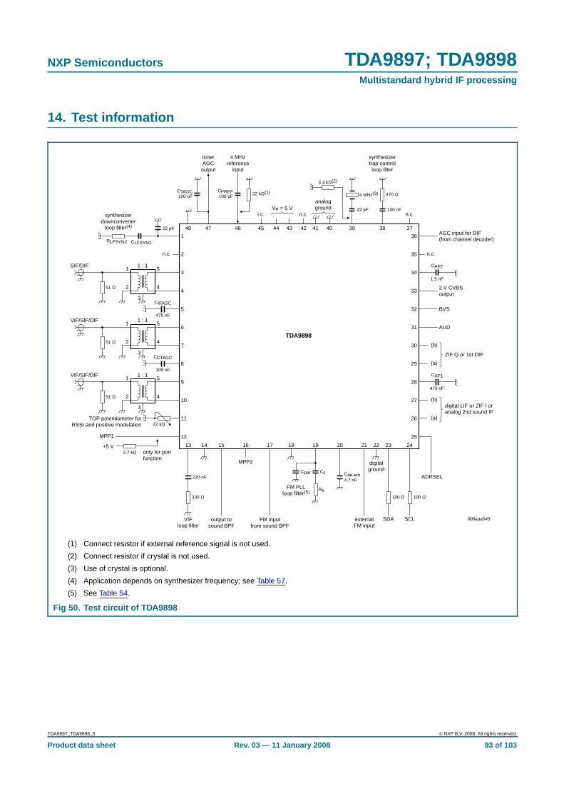
NXP Semiconductors TDA9897; TDA9898Multistandard hybrid IF processing
14. Test information
(1) Connect resistor if external reference signal is not used.
(2) Connect resistor if crystal is not used.
(3) Use of crystal is optional.
(4) Application depends on synthesizer frequency; see Table 57.
(5) See Table 54.
Fig 50. Test circuit of TDA9898
008aaa045
22 pF
22 kΩ(1)
synthesizerdownconverter
loop filter(4)
100 nF
470 Ω
synthesizertrap controlloop filter
CAF2
1.5 nF
CAF1
470 nF
SIF/DIF
1
48 45
i.c.
42 38
3.3 kΩ(2)
39
n.c.
37
n.c.
44 4347
CTAGC100 nF
tunerAGC
output
51 Ω
2
5
31
1 : 1
2
5
4
3
46
CFREF100 pF
4 MHzreference
input
VP = 5 V
41 40
analogground
4
TDA98986
7
8
n.c.
MPP2
output tosound BPF
FM inputfrom sound BPF
AGC input for DIF(from channel decoder)
BVS
2 V CVBSoutput
AUD
ZIF Q or 1st DIF
(b)
(a)
digital LIF or ZIF I oranalog 2nd sound IF
(b)
(a)
9
10
11
12
13 14 221815 16 17
36
35
32
34
33
31
30
29
28
27
26
25MPP1
+5 V
VIFloop filter
externalFM input
digitalground
21
ADRSEL
SDA
TOP potentiometer forRSSI and positive modulation
only for portfunction
22 kΩ
2.7 kΩ
330 Ω
220 nF
19
100 Ω
20 23
SCL
100 Ω
24
4.7 nFCde-em
VIF/SIF/DIF
51 Ω
11 : 1
2
5
4
3
VIF/SIF/DIF
51 Ω
11 : 1
2
5
4
3
470 nF
CIFAGC
100 nF
CCTAGC
RLFSYN2 CLFSYN2
22 pF
4 MHz(3)
n.c.
FM PLLloop filter(5) Rs
Cpar Cs
TDA9897_TDA9898_3 © NXP B.V. 2008. All rights reserved.
Product data sheet Rev. 03 — 11 January 2008 93 of 103

NXP Semiconductors TDA9897; TDA9898Multistandard hybrid IF processing
(1) Connect resistor if external reference signal is not used.
(2) Connect resistor if crystal is not used.
(3) Use of crystal is optional.
(4) Application depends on synthesizer frequency; see Table 57.
(5) See Table 54.
Fig 51. Test circuit of TDA9897
008aaa044
22 pF
22 kΩ(1)
synthesizerdownconverter
loop filter(4)
100 nF
470 Ω
synthesizertrap controlloop filter
CAF2
1.5 nF
CAF1
470 nF
SIF/DIF
1
48 45
i.c.
42 38
3.3 kΩ(2)
39
n.c.
37
n.c.
44 4347
CTAGC100 nF
tunerAGC
output
51 Ω
2
5
31
1 : 1
2
5
4
3
46
CFREF100 pF
4 MHzreference
input
VP = 5 V
41 40
analogground
4
TDA98976
7
8
n.c.
MPP2
output tosound BPF
FM inputfrom sound BPF
AGC input for DIF(from channel decoder)
BVS
2 V CVBSoutput
AUD
ZIF Q or 1st DIF
(b)
(a)
digital LIF or ZIF I oranalog 2nd sound IF
(b)
(a)
9
10
11
12
13 14 221815 16 17
36
35
32
34
33
31
30
29
28
27
26
25MPP1
+5 V
VIFloop filter
externalFM input
digitalground
21
ADRSEL
SDA
TOP potentiometer for RSSIand IF based tuner AGC
only for portfunction
22 kΩ
2.7 kΩ
330 Ω
220 nF
19
100 Ω
20 23
SCL
100 Ω
24
4.7 nFCde-em
n.c.
VIF/SIF/DIF1
1 : 1
2
5
4
3
VIF/SIF/DIF
51 Ω
11 : 1
2
5
4
3
RLFSYN2 CLFSYN2
22 pF
4 MHz(3)
n.c.
FM PLLloop filter(5) Rs
Cpar Cs
100 nF
CCTAGC
51 Ω
TDA9897_TDA9898_3 © NXP B.V. 2008. All rights reserved.
Product data sheet Rev. 03 — 11 January 2008 94 of 103

NXP Semiconductors TDA9897; TDA9898Multistandard hybrid IF processing
15. Package outline
Fig 52. Package outline SOT313-2 (LQFP48)
UNITA
max. A1 A2 A3 bp c E(1) e HE L L p Zywv θ
REFERENCESOUTLINEVERSION
EUROPEANPROJECTION ISSUE DATE
IEC JEDEC JEITA
mm 1.6 0.200.05
1.451.35
0.250.270.17
0.180.12
7.16.9 0.5
9.158.85
0.950.55
70
o
o0.12 0.10.21
DIMENSIONS (mm are the original dimensions)
Note
1. Plastic or metal protrusions of 0.25 mm maximum per side are not included.
0.750.45
SOT313-2 MS-026136E0500-01-1903-02-25
D(1) (1)(1)
7.16.9
HD
9.158.85
EZ
0.950.55
D
bp
e
E
B
12
DH
bp
EH
v M B
D
ZD
A
ZE
e
v M A
1
48
37
36 25
24
13
θ
A1A
Lp
detail X
L
(A )3A2
X
y
c
w M
w M
0 2.5 5 mm
scale
pin 1 index
LQFP48: plastic low profile quad flat package; 48 leads; body 7 x 7 x 1.4 mm SOT313-2
TDA9897_TDA9898_3 © NXP B.V. 2008. All rights reserved.
Product data sheet Rev. 03 — 11 January 2008 95 of 103

NXP Semiconductors TDA9897; TDA9898Multistandard hybrid IF processing
Fig 53. Package outline SOT619-1 (HVQFN48)
0.51
A1 EhbUNIT ye
0.2
c
REFERENCESOUTLINEVERSION
EUROPEANPROJECTION ISSUE DATE
IEC JEDEC JEITA
mm 7.16.9
Dh
5.254.95
y1
7.16.9
5.254.95
e1
5.5
e2
5.50.300.18
0.050.00
0.05 0.1
DIMENSIONS (mm are the original dimensions)
SOT619-1 MO-220 - - -- - -
0.50.3
L
0.1
v
0.05
w
0 2.5 5 mm
scale
SOT619-1HVQFN48: plastic thermal enhanced very thin quad flat package; no leads;48 terminals; body 7 x 7 x 0.85 mm
A(1)
max.
AA1
c
detail X
yy1 Ce
L
Eh
Dh
e
e1
b
13 24
48 37
36
2512
1
X
D
E
C
B A
e2
01-08-0802-10-18
terminal 1index area
terminal 1index area
1/2 e
1/2 e ACC
Bv M
w M
E(1)
Note
1. Plastic or metal protrusions of 0.075 mm maximum per side are not included.
D(1)
TDA9897_TDA9898_3 © NXP B.V. 2008. All rights reserved.
Product data sheet Rev. 03 — 11 January 2008 96 of 103

NXP Semiconductors TDA9897; TDA9898Multistandard hybrid IF processing
16. Soldering
16.1 IntroductionThere is no soldering method that is ideal for all surface mount IC packages. Wavesoldering can still be used for certain surface mount ICs, but it is not suitable for fine pitchSMDs. In these situations reflow soldering is recommended.
16.2 Through-hole mount packages
16.2.1 Soldering by dipping or by solder wave
Typical dwell time of the leads in the wave ranges from 3 seconds to 4 seconds at 250 °Cor 265 °C, depending on solder material applied, SnPb or Pb-free respectively.
The total contact time of successive solder waves must not exceed 5 seconds.
The device may be mounted up to the seating plane, but the temperature of the plasticbody must not exceed the specified maximum storage temperature (Tstg(max)). If theprinted-circuit board has been pre-heated, forced cooling may be necessary immediatelyafter soldering to keep the temperature within the permissible limit.
16.2.2 Manual soldering
Apply the soldering iron (24 V or less) to the lead(s) of the package, either below theseating plane or not more than 2 mm above it. If the temperature of the soldering iron bit isless than 300 °C it may remain in contact for up to 10 seconds. If the bit temperature isbetween 300 °C and 400 °C, contact may be up to 5 seconds.
16.3 Surface mount packages
16.3.1 Reflow soldering
Key characteristics in reflow soldering are:
• Lead-free versus SnPb soldering; note that a lead-free reflow process usually leads tohigher minimum peak temperatures (see Figure 54) than a PbSn process, thusreducing the process window
• Solder paste printing issues including smearing, release, and adjusting the processwindow for a mix of large and small components on one board
• Reflow temperature profile; this profile includes preheat, reflow (in which the board isheated to the peak temperature) and cooling down. It is imperative that the peaktemperature is high enough for the solder to make reliable solder joints (a solder pastecharacteristic). In addition, the peak temperature must be low enough that thepackages and/or boards are not damaged. The peak temperature of the packagedepends on package thickness and volume and is classified in accordance withTable 58 and 59
TDA9897_TDA9898_3 © NXP B.V. 2008. All rights reserved.
Product data sheet Rev. 03 — 11 January 2008 97 of 103

NXP Semiconductors TDA9897; TDA9898Multistandard hybrid IF processing
Moisture sensitivity precautions, as indicated on the packing, must be respected at alltimes.
Studies have shown that small packages reach higher temperatures during reflowsoldering, see Figure 54.
For further information on temperature profiles, refer to Application Note AN10365“Surface mount reflow soldering description”.
16.3.2 Wave soldering
Conventional single wave soldering is not recommended for surface mount devices(SMDs) or printed-circuit boards with a high component density, as solder bridging andnon-wetting can present major problems.
Table 58. SnPb eutectic process (from J-STD-020C)
Package thickness (mm) Package reflow temperature ( °C)
Volume (mm 3)
< 350 ≥ 350
< 2.5 235 220
≥ 2.5 220 220
Table 59. Lead-free process (from J-STD-020C)
Package thickness (mm) Package reflow temperature ( °C)
Volume (mm 3)
< 350 350 to 2000 > 2000
< 1.6 260 260 260
1.6 to 2.5 260 250 245
> 2.5 250 245 245
MSL: Moisture Sensitivity Level
Fig 54. Temperature profiles for large and small components
001aac844
temperature
time
minimum peak temperature= minimum soldering temperature
maximum peak temperature= MSL limit, damage level
peak temperature
TDA9897_TDA9898_3 © NXP B.V. 2008. All rights reserved.
Product data sheet Rev. 03 — 11 January 2008 98 of 103
NXP Semiconductors TDA9897; TDA9898Multistandard hybrid IF processing
To overcome these problems the double-wave soldering method was specificallydeveloped.
If wave soldering is used the following conditions must be observed for optimal results:
• Use a double-wave soldering method comprising a turbulent wave with high upwardpressure followed by a smooth laminar wave.
• For packages with leads on two sides and a pitch (e):
– larger than or equal to 1.27 mm, the footprint longitudinal axis is preferred to beparallel to the transport direction of the printed-circuit board;
– smaller than 1.27 mm, the footprint longitudinal axis must be parallel to thetransport direction of the printed-circuit board.
The footprint must incorporate solder thieves at the downstream end.
• For packages with leads on four sides, the footprint must be placed at a 45° angle tothe transport direction of the printed-circuit board. The footprint must incorporatesolder thieves downstream and at the side corners.
During placement and before soldering, the package must be fixed with a droplet ofadhesive. The adhesive can be applied by screen printing, pin transfer or syringedispensing. The package can be soldered after the adhesive is cured.
Typical dwell time of the leads in the wave ranges from 3 seconds to 4 seconds at 250 °Cor 265 °C, depending on solder material applied, SnPb or Pb-free respectively.
A mildly-activated flux will eliminate the need for removal of corrosive residues in mostapplications.
16.3.3 Manual soldering
Fix the component by first soldering two diagonally-opposite end leads. Use a low voltage(24 V or less) soldering iron applied to the flat part of the lead. Contact time must belimited to 10 seconds at up to 300 °C.
When using a dedicated tool, all other leads can be soldered in one operation within2 seconds to 5 seconds between 270 °C and 320 °C.
16.4 Package related soldering information
Table 60. Suitability of IC packages for wave, reflow and dipping soldering methods
Mounting Package [1] Soldering method
Wave Reflow [2] Dipping
Through-hole mount CPGA, HCPGA suitable − −
DBS, DIP, HDIP, RDBS, SDIP, SIL suitable[3] − suitable
Through-hole-surfacemount
PMFP[4] not suitable not suitable −
TDA9897_TDA9898_3 © NXP B.V. 2008. All rights reserved.
Product data sheet Rev. 03 — 11 January 2008 99 of 103

NXP Semiconductors TDA9897; TDA9898Multistandard hybrid IF processing
[1] For more detailed information on the BGA packages refer to the (LF)BGA Application Note (AN01026); order a copy from your NXPSemiconductors sales office.
[2] All surface mount (SMD) packages are moisture sensitive. Depending upon the moisture content, the maximum temperature (withrespect to time) and body size of the package, there is a risk that internal or external package cracks may occur due to vaporization ofthe moisture in them (the so called popcorn effect).
[3] For SDIP packages, the longitudinal axis must be parallel to the transport direction of the printed-circuit board.
[4] Hot bar soldering or manual soldering is suitable for PMFP packages.
[5] These transparent plastic packages are extremely sensitive to reflow soldering conditions and must on no account be processedthrough more than one soldering cycle or subjected to infrared reflow soldering with peak temperature exceeding 217 °C ± 10 °Cmeasured in the atmosphere of the reflow oven. The package body peak temperature must be kept as low as possible.
[6] These packages are not suitable for wave soldering. On versions with the heatsink on the bottom side, the solder cannot penetratebetween the printed-circuit board and the heatsink. On versions with the heatsink on the top side, the solder might be deposited on theheatsink surface.
[7] If wave soldering is considered, then the package must be placed at a 45° angle to the solder wave direction. The package footprintmust incorporate solder thieves downstream and at the side corners.
[8] Wave soldering is suitable for LQFP, QFP and TQFP packages with a pitch (e) larger than 0.8 mm; it is definitely not suitable forpackages with a pitch (e) equal to or smaller than 0.65 mm.
[9] Wave soldering is suitable for SSOP, TSSOP, VSO and VSSOP packages with a pitch (e) equal to or larger than 0.65 mm; it is definitelynot suitable for packages with a pitch (e) equal to or smaller than 0.5 mm.
[10] Image sensor packages in principle should not be soldered. They are mounted in sockets or delivered pre-mounted on flex foil.However, the image sensor package can be mounted by the client on a flex foil by using a hot bar soldering process. The appropriatesoldering profile can be provided on request.
17. Abbreviations
Surface mount BGA, HTSSON..T[5], LBGA,LFBGA, SQFP, SSOP..T[5], TFBGA,VFBGA, XSON
not suitable suitable −
DHVQFN, HBCC, HBGA, HLQFP,HSO, HSOP, HSQFP, HSSON,HTQFP, HTSSOP, HVQFN,HVSON, SMS
not suitable[6] suitable −
PLCC[7], SO, SOJ suitable suitable −
LQFP, QFP, TQFP not recommended[7][8] suitable −
SSOP, TSSOP, VSO, VSSOP not recommended[9] suitable −
CWQCCN..L[10], WQCCN..L[10] not suitable not suitable −
Table 60. Suitability of IC packages for wave, reflow and dipping soldering methods …continued
Mounting Package [1] Soldering method
Wave Reflow [2] Dipping
Table 61. Abbreviations
Acronym Description
ADC Analog-to-Digital Converter
AFC Automatic Frequency Control
AGC Automatic Gain Control
ATV Analog TV
BP Band-Pass
CW Continuous Wave
DAC Digital-to-Analog Converter
DC Direct Current
TDA9897_TDA9898_3 © NXP B.V. 2008. All rights reserved.
Product data sheet Rev. 03 — 11 January 2008 100 of 103

NXP Semiconductors TDA9897; TDA9898Multistandard hybrid IF processing
18. Revision history
DIF Digital Intermediate Frequency
DSP Digital Signal Processor
DTV Digital TV
DVB Digital Video Broadcast
ESD ElectroStatic Discharge
FPLL Frequency Phase-Locked Loop
IC Integrated Circuit
IF Intermediate Frequency
LCD Liquid Crystal Display
LIF Low Intermediate Frequency
MAD Module Address
NICAM Near Instantaneous Companded Audio Multiplex
PLL Phase-Locked Loop
POR Power-On Reset
QSS Quasi Split Sound
RIF Radio Intermediate Frequency
RSSI Received Signal Strength Indication
SAW Surface Acoustic Wave
SC Sound Carrier
SIF Sound Intermediate Frequency
TAGC Tuner Automatic Gain Control
TOP TakeOver Point
VCO Voltage-Controlled Oscillator
VIF Vision Intermediate Frequency
VITS Vertical Interval Test Signal
ZIF Zero Intermediate Frequency
Table 62. Revision history
Document ID Release date Data sheet status Change notice Supersedes
TDA9897_TDA9898_3 20080111 Product data sheet - TDA9897_TDA9898_2
Modifications: • Additional specification of features for V2/S1 version
TDA9897_TDA9898_2 20070411 Product data sheet - TDA9897_TDA9898_1
TDA9897_TDA9898_1 20060922 Product data sheet - -
Table 61. Abbreviations …continued
Acronym Description
TDA9897_TDA9898_3 © NXP B.V. 2008. All rights reserved.
Product data sheet Rev. 03 — 11 January 2008 101 of 103

NXP Semiconductors TDA9897; TDA9898Multistandard hybrid IF processing
19. Legal information
19.1 Data sheet status
[1] Please consult the most recently issued document before initiating or completing a design.
[2] The term ‘short data sheet’ is explained in section “Definitions”.
[3] The product status of device(s) described in this document may have changed since this document was published and may differ in case of multiple devices. The latest product statusinformation is available on the Internet at URL http://www.nxp.com.
19.2 Definitions
Draft — The document is a draft version only. The content is still underinternal review and subject to formal approval, which may result inmodifications or additions. NXP Semiconductors does not give anyrepresentations or warranties as to the accuracy or completeness ofinformation included herein and shall have no liability for the consequences ofuse of such information.
Short data sheet — A short data sheet is an extract from a full data sheetwith the same product type number(s) and title. A short data sheet is intendedfor quick reference only and should not be relied upon to contain detailed andfull information. For detailed and full information see the relevant full datasheet, which is available on request via the local NXP Semiconductors salesoffice. In case of any inconsistency or conflict with the short data sheet, thefull data sheet shall prevail.
19.3 Disclaimers
General — Information in this document is believed to be accurate andreliable. However, NXP Semiconductors does not give any representations orwarranties, expressed or implied, as to the accuracy or completeness of suchinformation and shall have no liability for the consequences of use of suchinformation.
Right to make changes — NXP Semiconductors reserves the right to makechanges to information published in this document, including withoutlimitation specifications and product descriptions, at any time and withoutnotice. This document supersedes and replaces all information supplied priorto the publication hereof.
Suitability for use — NXP Semiconductors products are not designed,authorized or warranted to be suitable for use in medical, military, aircraft,space or life support equipment, nor in applications where failure ormalfunction of an NXP Semiconductors product can reasonably be expected
to result in personal injury, death or severe property or environmentaldamage. NXP Semiconductors accepts no liability for inclusion and/or use ofNXP Semiconductors products in such equipment or applications andtherefore such inclusion and/or use is at the customer’s own risk.
Applications — Applications that are described herein for any of theseproducts are for illustrative purposes only. NXP Semiconductors makes norepresentation or warranty that such applications will be suitable for thespecified use without further testing or modification.
Limiting values — Stress above one or more limiting values (as defined inthe Absolute Maximum Ratings System of IEC 60134) may cause permanentdamage to the device. Limiting values are stress ratings only and operation ofthe device at these or any other conditions above those given in theCharacteristics sections of this document is not implied. Exposure to limitingvalues for extended periods may affect device reliability.
Terms and conditions of sale — NXP Semiconductors products are soldsubject to the general terms and conditions of commercial sale, as publishedat http://www.nxp.com/profile/terms, including those pertaining to warranty,intellectual property rights infringement and limitation of liability, unlessexplicitly otherwise agreed to in writing by NXP Semiconductors. In case ofany inconsistency or conflict between information in this document and suchterms and conditions, the latter will prevail.
No offer to sell or license — Nothing in this document may be interpretedor construed as an offer to sell products that is open for acceptance or thegrant, conveyance or implication of any license under any copyrights, patentsor other industrial or intellectual property rights.
19.4 TrademarksNotice: All referenced brands, product names, service names and trademarksare the property of their respective owners.
I2C-bus — logo is a trademark of NXP B.V.
20. Contact information
For additional information, please visit: http://www .nxp.com
For sales office addresses, send an email to: salesad [email protected]
Document status [1] [2] Product status [3] Definition
Objective [short] data sheet Development This document contains data from the objective specification for product development.
Preliminary [short] data sheet Qualification This document contains data from the preliminary specification.
Product [short] data sheet Production This document contains the product specification.
TDA9897_TDA9898_3 © NXP B.V. 2008. All rights reserved.
Product data sheet Rev. 03 — 11 January 2008 102 of 103
NXP Semiconductors TDA9897; TDA9898Multistandard hybrid IF processing
21. Contents
1 General description . . . . . . . . . . . . . . . . . . . . . . 12 Features . . . . . . . . . . . . . . . . . . . . . . . . . . . . . . . 12.1 General . . . . . . . . . . . . . . . . . . . . . . . . . . . . . . . 12.2 Analog TV processing. . . . . . . . . . . . . . . . . . . . 12.3 Digital TV processing . . . . . . . . . . . . . . . . . . . . 22.4 Dual mode . . . . . . . . . . . . . . . . . . . . . . . . . . . . 32.5 FM radio mode . . . . . . . . . . . . . . . . . . . . . . . . . 33 Applications . . . . . . . . . . . . . . . . . . . . . . . . . . . . 34 Quick reference data . . . . . . . . . . . . . . . . . . . . . 35 Ordering information . . . . . . . . . . . . . . . . . . . . . 76 Block diagram . . . . . . . . . . . . . . . . . . . . . . . . . . 87 Pinning information . . . . . . . . . . . . . . . . . . . . . 127.1 Pinning . . . . . . . . . . . . . . . . . . . . . . . . . . . . . . 127.2 Pin description . . . . . . . . . . . . . . . . . . . . . . . . 138 Functional description . . . . . . . . . . . . . . . . . . 148.1 IF input switch. . . . . . . . . . . . . . . . . . . . . . . . . 148.2 VIF demodulator . . . . . . . . . . . . . . . . . . . . . . . 158.3 VIF AGC and tuner AGC. . . . . . . . . . . . . . . . . 158.3.1 Mode selection of VIF AGC . . . . . . . . . . . . . . 158.3.2 VIF AGC monitor . . . . . . . . . . . . . . . . . . . . . . 158.3.3 Tuner AGC . . . . . . . . . . . . . . . . . . . . . . . . . . . 158.4 DIF/SIF FM and AM sound AGC . . . . . . . . . . 168.5 Frequency phase-locked loop for VIF . . . . . . . 168.6 DIF/SIF converter stage . . . . . . . . . . . . . . . . . 168.7 Mono sound demodulator . . . . . . . . . . . . . . . . 178.7.1 Narrow-band FM PLL demodulation. . . . . . . . 178.7.2 AM sound demodulation . . . . . . . . . . . . . . . . . 178.8 Audio amplifier . . . . . . . . . . . . . . . . . . . . . . . . 178.9 Synthesizer . . . . . . . . . . . . . . . . . . . . . . . . . . . 178.10 I2C-bus transceiver and slave address . . . . . . 189 I2C-bus control . . . . . . . . . . . . . . . . . . . . . . . . . 189.1 Read format . . . . . . . . . . . . . . . . . . . . . . . . . . 199.2 Write format . . . . . . . . . . . . . . . . . . . . . . . . . . 229.2.1 Subaddress. . . . . . . . . . . . . . . . . . . . . . . . . . . 239.2.2 Description of data bytes . . . . . . . . . . . . . . . . 2410 Limiting values. . . . . . . . . . . . . . . . . . . . . . . . . 3711 Thermal characteristics. . . . . . . . . . . . . . . . . . 3712 Characteristics . . . . . . . . . . . . . . . . . . . . . . . . . 3812.1 Analog TV signal processing . . . . . . . . . . . . . 3812.2 Digital TV signal processing . . . . . . . . . . . . . . 7613 Application information. . . . . . . . . . . . . . . . . . 9014 Test information . . . . . . . . . . . . . . . . . . . . . . . . 9315 Package outline . . . . . . . . . . . . . . . . . . . . . . . . 9516 Soldering . . . . . . . . . . . . . . . . . . . . . . . . . . . . . 9716.1 Introduction . . . . . . . . . . . . . . . . . . . . . . . . . . 97
16.2 Through-hole mount packages . . . . . . . . . . . 9716.2.1 Soldering by dipping or by solder wave . . . . . 9716.2.2 Manual soldering . . . . . . . . . . . . . . . . . . . . . . 9716.3 Surface mount packages . . . . . . . . . . . . . . . . 9716.3.1 Reflow soldering. . . . . . . . . . . . . . . . . . . . . . . 9716.3.2 Wave soldering. . . . . . . . . . . . . . . . . . . . . . . . 9816.3.3 Manual soldering . . . . . . . . . . . . . . . . . . . . . . 9916.4 Package related soldering information . . . . . . 9917 Abbreviations . . . . . . . . . . . . . . . . . . . . . . . . 10018 Revision history . . . . . . . . . . . . . . . . . . . . . . 10119 Legal information . . . . . . . . . . . . . . . . . . . . . 10219.1 Data sheet status . . . . . . . . . . . . . . . . . . . . . 10219.2 Definitions . . . . . . . . . . . . . . . . . . . . . . . . . . 10219.3 Disclaimers. . . . . . . . . . . . . . . . . . . . . . . . . . 10219.4 Trademarks . . . . . . . . . . . . . . . . . . . . . . . . . 10220 Contact information . . . . . . . . . . . . . . . . . . . 10221 Contents. . . . . . . . . . . . . . . . . . . . . . . . . . . . . 103
© NXP B.V. 2008. All rights reserved.For more information, please visit: http://www.nxp.comFor sales office addresses, please send an email to: [email protected]
Date of release: 11 January 2008
Document identifier: TDA9897_TDA9898_3
Please be aware that important notices concerning this document and the product(s)described herein, have been included in section ‘Legal information’.