Embed Size (px)
Citation preview

DATA SHEET
Product specificationSupersedes data of 2002 Jul 03
2002 Aug 27
INTEGRATED CIRCUITS
TEA1552GreenChipII SMPS control IC
2002 Aug 27 2
Philips Semiconductors Product specification
GreenChip II SMPS control IC TEA1552
FEATURES
Distinctive features
• Universal mains supply operation (70 to 276 V AC)
• High level of integration, giving a very low externalcomponent count.
Green features
• Valley or zero voltage switching for minimum switchinglosses
• Efficient quasi-resonant operation at high power levels
• Frequency reduction at low power standby for improvedsystem efficiency (<3 W)
• Cycle skipping mode at very low loads. Pi < 300 mW atno-load operation for a typical adapter application
• On-chip start-up current source
• Standby indication pin to indicate low output powerconsumption.
Protection features
• Safe restart mode for system fault conditions
• Continuous mode protection by means ofdemagnetization detection (zero switch-on current)
• Accurate and adjustable overvoltage protection(latched)
• Short winding protection
• Undervoltage protection (foldback during overload)
• Overtemperature protection (latched)
• Low and adjustable overcurrent protection trip level
• Soft (re)start
• Mains voltage-dependent operation-enabling level
• General purpose input for lock protection.
APPLICATIONS
Typical application areas are adapters and chargers (e.g.for laptops, camcorders and printers) and all applicationsthat demand an efficient and cost-effective solution up to250 W.
GENERAL DESCRIPTION
The GreenChip(1)II is the second generation of greenSwitched Mode Power Supply (SMPS) control ICsoperating directly from the rectified universal mains. A highlevel of integration leads to a cost effective power supplywith a very low number of external components.
The special built-in green functions allow the efficiency tobe optimum at all power levels. This holds forquasi-resonant operation at high power levels, as well asfixed frequency operation with valley switching at mediumpower levels. At low power (standby) levels, the systemoperates at reduced frequency and with valley detection.
The proprietary high voltage BCD800 process makesdirect start-up possible from the rectified mains voltage inan effective and green way. A second low voltageBICMOS IC is used for accurate, high speed protectionfunctions and control.
Highly efficient, reliable supplies can easily be designedusing the GreenChipII control IC.
(1) GreenChip is a trademark of Koninklijke PhilipsElectronics N.V.

2002 Aug 27 3
Philips Semiconductors Product specification
GreenChipII SMPS control IC TEA1552
ORDERING INFORMATION
TYPENUMBER
PACKAGE
NAME DESCRIPTION VERSION
TEA1552T SO14 plastic small outline package; 14 leads; body width 3.9 mm SOT108-1
handbook, full pagewidth
MBL498
TEA1552T
1
2
3
4
5
6
7
14
13
12
11
10
9
8
VCOadj
Isense
STDBY
DRIVER
HVS
HVS
DRAIN
DEM
CTRL
LOCK
VCC(5V)
GND
n.c.
VCC
Fig.1 Basic application.
2002 Aug 27 4
Philips Semiconductors Product specification
GreenChipII SMPS control IC TEA1552
BLOCK DIAGRAM
handbook, full pagewidthSUPPLY
MANAGEMENT
internalsupply
UVLO start
M-level
VCC8
10
13
300 Ω
1
3
GND
STDBY
S1
CTRL
FREQUENCYCONTROL
VOLTAGECONTROLLEDOSCILLATOR
LOGIC
LOGIC
OVER-VOLTAGE
PROTECTION
OVER-POWERPROTECTION
shortwinding
softstartS2
OVER-TEMPERATUREPROTECTION
S Q
RUVLO Q
MAXIMUMON-TIME
PROTECTION
POWER-ONRESET
−1
VALLEY
TEA1552
100 mV
clamp
DRIVER
START-UPCURRENT SOURCE
12LOCK
VCOadj
0.88 V
0.5 V
5.6 V
2
11
Isense
VCC(5V)
4DRIVER
MBL499
14DEM
7DRAIN
5, 6HVS
OCP
LEB
blank
Iss
lockdetect
2.5 V
S Q
RVCC < 4.5 V Q
5 V/1 mA(max)
Fig.2 Block diagram.
2002 Aug 27 5
Philips Semiconductors Product specification
GreenChipII SMPS control IC TEA1552
PINNING FUNCTIONAL DESCRIPTION
The TEA1552 is the controller of a compact flybackconverter, with the IC situated at the primary side.An auxiliary winding of the transformer providesdemagnetization detection and powers the IC afterstart-up.
The TEA1552 operates in multi modes (see Fig.4).
The next converter stroke is started only afterdemagnetization of the transformer current (zero currentswitching), while the drain voltage has reached the lowestvoltage to prevent switching losses (green function). Theprimary resonant circuit of primary inductance and draincapacitor ensures this quasi-resonant operation. Thedesign can be optimized in such a way that zero voltageswitching can be reached over almost the completeuniversal mains range.
To prevent very high frequency operation at lower loads,the quasi-resonant operation changes smoothly in fixedfrequency PWM control.
At very low power (standby) levels, the frequency iscontrolled down, via the VCO, to a minimum frequency ofapproximately 25 kHz.
Start-up, mains enabling operation level andundervoltage lock-out (see Figs 11 and 12)
Initially, the IC is self supplying from the rectified mainsvoltage via pin DRAIN. Supply capacitor CVCC is chargedby the internal start-up current source to a level ofapproximately 4 V or higher, depending on the drainvoltage. Once the drain voltage exceeds the M-level(mains-dependent operation-enabling level), the start-upcurrent source will continue charging capacitor CVCC(switch S1 will be opened); see Fig.2. The IC will activatethe power converter as soon as the voltage on pin VCCpasses the level VCC(start). The IC supply is taken over bythe auxiliary winding as soon as the output voltagereaches its intended level and the IC supply from themains voltage is subsequently stopped for high efficiencyoperation (green function).
The moment the voltage on pin VCC drops below theundervoltage lock-out level VUVLO, the IC stops switchingand enters a safe restart from the rectified mains voltage.Inhibiting the auxiliary supply by external means causesthe converter to operate in a stable, well defined burstmode.
Supply management
All (internal) reference voltages are derived from atemperature compensated, on-chip band gap circuit.
SYMBOL PIN DESCRIPTION
VCOadj 1 VCO adjustment input
Isense 2 programmable current sense input
STDBY 3 standby indication or control output
DRIVER 4 gate driver output
HVS 5 high voltage safety spacer, notconnected
HVS 6 high voltage safety spacer, notconnected
DRAIN 7 drain of external MOS switch, input forstart-up current and valley sensing
VCC 8 supply voltage
n.c. 9 not connected
GND 10 ground
VCC(5V) 11 5 V output
LOCK 12 lock input
CTRL 13 control input
DEM 14 input from auxiliary winding fordemagnetization timing, OVP and OPP
handbook, halfpage
TEA1552T
MBL497
1
2
3
4
5
6
7
VCOadj
Isense
STDBY
DRIVER
HVS
HVS
DRAIN
DEM
CTRL
LOCK
VCC(5V)
GND
n.c.
VCC
14
13
12
11
10
9
8
Fig.3 Pin configuration.

2002 Aug 27 6
Philips Semiconductors Product specification
GreenChipII SMPS control IC TEA1552
Current mode control
Current mode control is used for its good line regulationbehaviour.
The ‘on-time’ is controlled by the internally inverted controlpin voltage, which is compared with the primary currentinformation. The primary current is sensed across anexternal resistor. The driver output is latched in the logic,preventing multiple switch-on.
The internal control voltage is inversely proportional to theexternal control pin voltage, with an offset of 1.5 V. Thismeans that a voltage range from 1 to 1.5 V on pin CTRLwill result in an internal control voltage range from0.5 to 0 V (a high external control voltage results in a lowduty cycle).
Oscillator
The maximum fixed frequency of the oscillator is set by aninternal current source and capacitor. The maximumfrequency is reduced once the control voltage enters theVCO control window. Then, the maximum frequencychanges linearly with the control voltage until the minimumfrequency is reached (see Figs 5 and 6).
VCO adjustment
The VCOadj pin can be used to set the VCO operationpoint. As soon as the peak voltage on the sense resistor iscontrolled below half the voltage on the VCOadj pin (VCO1level), frequency reduction will start. The actual peakvoltage on sense will be somewhat higher due to switch-offdelay (see Fig.7). The frequency reduction will stopapproximately 25 mV lower (VCO2 level), when theminimum frequency is reached.
Cycle skipping
At very low power levels, a cycle skipping mode will beactivated. A high control voltage will reduce the switchingfrequency to a minimum of 25 kHz. If the voltage on thecontrol pin has raised even more, switch-on of the externalpower MOSFET will be inhibited until the voltage on thecontrol pin has dropped to a lower value again (see Fig.7).
For system accuracy, it is not the absolute voltage on thecontrol pin that will trigger the cycle skipping mode, but asignal derived from the internal VCO will be used.
Remark: If the no-load requirement of the system is suchthat the output voltage can be regulated to its intendedlevel at a switching frequency of 25 kHz or above, thecycle skipping mode will not be activated.
handbook, halfpageVCO fixed quasi resonant
P (W)
MBL500f
(kHz)
25
125
Fig.4 Multi mode operation.
handbook, halfpage
VCTRL1 V(typ)
0.52 V
1.5 V(typ)
MGU233Vsense(max)
Fig.5 Vsense(max) as a function of VCTRL.
handbook, halfpage
Vsense(max) (V)
MBL501f
(kHz)
25
125125 kHz
VCO2level
VCO1level
Fig.6 VCO frequency as a function of Vsense(max).

2002 Aug 27 7
Philips Semiconductors Product specification
GreenChipII SMPS control IC TEA1552
handbook, full pagewidth
MBL502
1.5 V − VCTRL
Isense
fosc
fmax
fmin
Vx (mV)
CTRL
VCC(5V)
VCOadj
currentcomparator
cycleskipping
X2
V
I
1
0
Vx
OSCILLATOR
DRIVERDRIVER
5 V
Vx (mV)
Vx (mV)dV4
VCOadj
dV2 dV1
dV3VSTDBY(V)
5
0
Fig.7 A functional implementation of the standby and cycle skipping circuitry.
The voltage levels dV1, dV2, dV3 and dV4 are fixed in the IC to typically 50 mV, 18 mV, 40 mV and 15 mV respectively.The level at which VCO mode of operation starts or ends can be externally controlled with the VCOadj pin.
Standby output
The STDBY output pin (VSTDBY = 5 V) can be used to drivean external NPN transistor or FET in order to e.g.switch-off a PFC circuit. The STDBY output is activated bythe internal VCO: as soon as the VCO has reduced theswitching frequency to (almost) the minimum frequency of25 kHz, the STDBY output will be activated (see Fig.7).The STDBY output will go low again as soon as the VCOallows a switching frequency close to the maximumfrequency of 125 kHz.
Demagnetization
The system will be in discontinuous conduction mode allthe time. The oscillator will not start a new primary strokeuntil the secondary stroke has ended.
Demagnetization features a cycle-by-cycle outputshort-circuit protection by immediately lowering thefrequency (longer off-time), thereby reducing the powerlevel.
Demagnetization recognition is suppressed during the firsttime (tsuppr). This suppression may be necessary inapplications where the transformer has a large leakageinductance and at low output voltages/start-up.
OverVoltage Protection (OVP)
An OVP mode is implemented in the GreenChip series.For the TEA1552, this works by sensing the auxiliaryvoltage via the current flowing into pin DEM during thesecondary stroke. The auxiliary winding voltage is awell-defined replica of the output voltage. Any voltagespikes are averaged by an internal filter.
If the output voltage exceeds the OVP trip level, the OVPcircuit switches off the power MOSFET. The controllerthen waits until the UVLO level is reached on pin VCC.When VCC drops to UVLO, capacitor CVCC will berecharged to the Vstart level, however the IC will not startswitching again. Subsequently, VCC will drop again to theUVLO level, etc.

2002 Aug 27 8
Philips Semiconductors Product specification
GreenChipII SMPS control IC TEA1552
Operation only recommences when the VCC voltage dropsbelow a level of approximately 4.5 V (practically when theVmains has been disconnected for a short period).
The output voltage (VOVP) at which the OVP function trips,can be set by the demagnetization resistor RDEM:
where Ns is the number of secondary turns and Naux is thenumber of auxiliary turns of the transformer.
Current IOVP(DEM) is internally trimmed.
The value of the demagnetization resistor (RDEM) can beadjusted to the turns ratio of the transformer, thus makingan accurate OVP possible.
Valley switching (see Fig.8)
A new cycle starts when the power switch is switched on.After the ‘on-time’ (which is determined by the ‘sense’voltage and the internal control voltage), the switch isopened and the secondary stroke starts.
After the secondary stroke, the drain voltage shows anoscillation with a frequency of approximately
where Lp is the primary self inductance of the transformerand Cd is the capacitance on the drain node.
VOVP
Ns
Naux------------ IOVP DEM( ) RDEM Vclamp DEM( ) pos( )+×[ ]×=
1
2 π× Lp Cd×( )×( )----------------------------------------------------
handbook, full pagewidth
drain
secondarystroke
MGU235
secondaryringing
primarystroke
valley
B A
secondarystroke
oscillator
A: Start of new cycle at lowest drain voltage.
B: Start of new cycle in a classical PWM system at high drain voltage.
Fig.8 Signals for valley switching.

2002 Aug 27 9
Philips Semiconductors Product specification
GreenChipII SMPS control IC TEA1552
As soon as the oscillator voltage is high again and thesecondary stroke has ended, the circuit waits for thelowest drain voltage before starting a new primary stroke.This method is called valley detection. Figure 8 shows thedrain voltage together with the valley signal, the signalindicating the secondary stroke and the oscillator signal.
In an optimum design, the reflected secondary voltage onthe primary side will force the drain voltage to zero. Thus,zero voltage switching is very possible, preventing large
capacitive switching losses , and
allowing high frequency operation, which results in smalland cost effective inductors.
OverCurrent Protection (OCP)
The cycle-by-cycle peak drain current limit circuit uses theexternal source resistor to measure the current accurately.This allows optimum size determination of the transformercore (cost issue). The circuit is activated after the leadingedge blanking time tleb. The OCP protection circuit limitsthe ‘sense’ voltage to an internal level.
OverPower Protection (OPP)
During the primary stroke, the rectified mains input voltageis measured by sensing the current drawn from pin DEM.This current is dependent on the mains voltage, according
to the following formula:
where:
The current information is used to adjust the peak draincurrent, which is measured via pin Isense. The internalcompensation is such that an almost mains independentmaximum output power can be realized.
The OPP curve is given in Fig.9.
Minimum and maximum ‘on-time’
The minimum ‘on-time’ of the SMPS is determined by theLeading Edge Blanking (LEB) time. The IC limits the‘on-time’ to 50 µs. When the system desires an ‘on-time’longer than 50 µs, a fault condition is assumed, and the ICwill stop switching and enter the safe restart mode.
Short winding protection
After the leading edge blanking time, the short windingprotection circuit is also activated. If the ‘sense’ voltageexceeds the short winding protection voltage Vswp, theconverter will stop switching. Once VCC drops below theUVLO level, capacitor CVCC will be recharged and thesupply will restart again. This cycle will be repeated untilthe short-circuit is removed (safe restart mode).
The short winding protection will also protect in case of asecondary diode short-circuit.
P12--- C V2 f×××=
IDEM
Vaux
RDEM---------------
N Vmains×RDEM
--------------------------≈ ≈
NNaux
Np------------=
handbook, halfpageMGU236
0.52 V(typ)
0.3 V(typ)
IDEM
Vsense(max)
−24 µA(typ)
−100 µA(typ)
Fig.9 OPP correction curve.
2002 Aug 27 10
Philips Semiconductors Product specification
GreenChipII SMPS control IC TEA1552
LOCK input
Pin LOCK is a general purpose (high-impedance) inputpin, which can be used to switch off the IC. As soon as thevoltage on this pin is raised above 2.5 V, switching will stopimmediately. The voltage on the VCC pin will cycle betweenVCC(start) and VCC(UVLO), but the IC will not start switchingagain until the latch function is reset. The latch is reset assoon as the VCC drops below 4.5 V (typical value). Theinternal OVP and OTP will also trigger this latch (seeFig.2).
The detection level of this input is related to the VCC(5V) pinvoltage in the following way: 0.5 × VCC(5V) ± 4%.An internal Zener diode clamp of 5.6 V will protect this pinfrom excessive voltages. No internal filtering is done onthis input.
OverTemperature Protection (OTP)
An accurate temperature protection is provided in thecircuit. When the junction temperature exceeds thethermal shutdown temperature, the IC will stop switching.When VCC drops to UVLO, capacitor CVCC will berecharged to the Vstart level, however the IC will not startswitching again. Subsequently, VCC will drop again to theUVLO level, etc.
Operation only recommences when the VCC voltage dropsbelow a level of approximately 4.5 V (practically when theVmains has been disconnected for a short period).
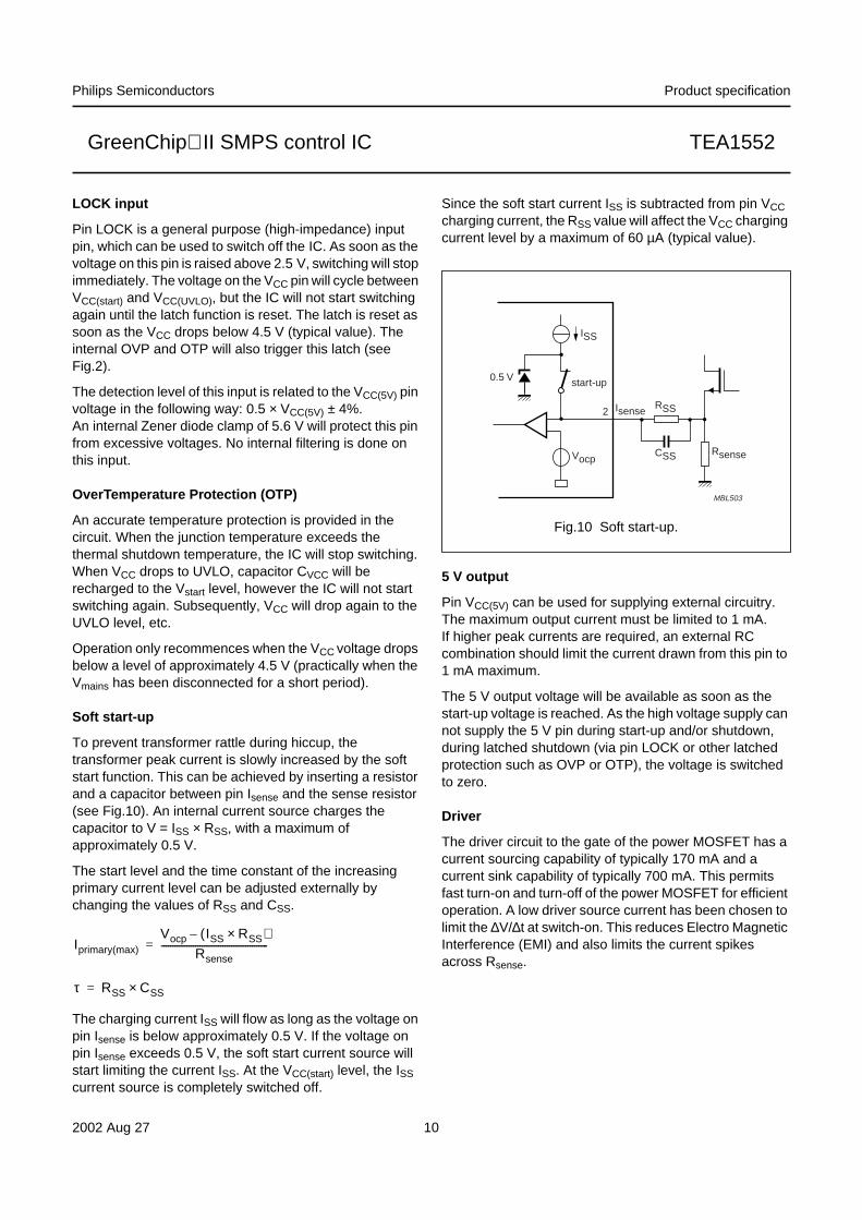
Soft start-up
To prevent transformer rattle during hiccup, thetransformer peak current is slowly increased by the softstart function. This can be achieved by inserting a resistorand a capacitor between pin Isense and the sense resistor(see Fig.10). An internal current source charges thecapacitor to V = ISS × RSS, with a maximum ofapproximately 0.5 V.
The start level and the time constant of the increasingprimary current level can be adjusted externally bychanging the values of RSS and CSS.
The charging current ISS will flow as long as the voltage onpin Isense is below approximately 0.5 V. If the voltage onpin Isense exceeds 0.5 V, the soft start current source willstart limiting the current ISS. At the VCC(start) level, the ISScurrent source is completely switched off.
Since the soft start current ISS is subtracted from pin VCCcharging current, the RSS value will affect the VCC chargingcurrent level by a maximum of 60 µA (typical value).
5 V output
Pin VCC(5V) can be used for supplying external circuitry.The maximum output current must be limited to 1 mA.If higher peak currents are required, an external RCcombination should limit the current drawn from this pin to1 mA maximum.
The 5 V output voltage will be available as soon as thestart-up voltage is reached. As the high voltage supply cannot supply the 5 V pin during start-up and/or shutdown,during latched shutdown (via pin LOCK or other latchedprotection such as OVP or OTP), the voltage is switchedto zero.
Driver
The driver circuit to the gate of the power MOSFET has acurrent sourcing capability of typically 170 mA and acurrent sink capability of typically 700 mA. This permitsfast turn-on and turn-off of the power MOSFET for efficientoperation. A low driver source current has been chosen tolimit the ∆V/∆t at switch-on. This reduces Electro MagneticInterference (EMI) and also limits the current spikesacross Rsense.
Iprimary(max)
Vocp ISS RSS×( )–
Rsense-----------------------------------------------=
τ RSS CSS×=
handbook, halfpage
CSS
RSSIsense
Rsense
ISS
Vocp
start-up
MBL503
2
0.5 V
Fig.10 Soft start-up.
2002 Aug 27 11
Philips Semiconductors Product specification
GreenChipII SMPS control IC TEA1552
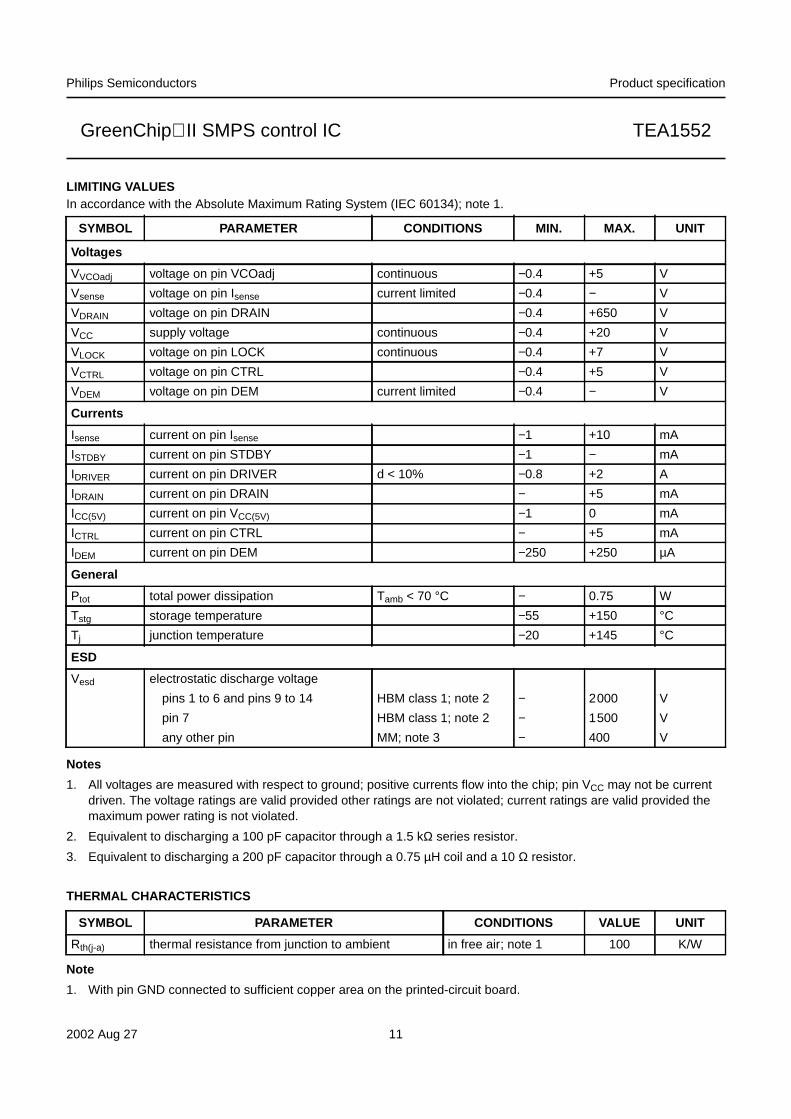
LIMITING VALUESIn accordance with the Absolute Maximum Rating System (IEC 60134); note 1.
Notes
1. All voltages are measured with respect to ground; positive currents flow into the chip; pin VCC may not be currentdriven. The voltage ratings are valid provided other ratings are not violated; current ratings are valid provided themaximum power rating is not violated.
2. Equivalent to discharging a 100 pF capacitor through a 1.5 kΩ series resistor.
3. Equivalent to discharging a 200 pF capacitor through a 0.75 µH coil and a 10 Ω resistor.
THERMAL CHARACTERISTICS
Note
1. With pin GND connected to sufficient copper area on the printed-circuit board.
SYMBOL PARAMETER CONDITIONS MIN. MAX. UNIT
Voltages
VVCOadj voltage on pin VCOadj continuous −0.4 +5 V
Vsense voltage on pin Isense current limited −0.4 − V
VDRAIN voltage on pin DRAIN −0.4 +650 V
VCC supply voltage continuous −0.4 +20 V
VLOCK voltage on pin LOCK continuous −0.4 +7 V
VCTRL voltage on pin CTRL −0.4 +5 V
VDEM voltage on pin DEM current limited −0.4 − V
Currents
Isense current on pin Isense −1 +10 mA
ISTDBY current on pin STDBY −1 − mA
IDRIVER current on pin DRIVER d < 10% −0.8 +2 A
IDRAIN current on pin DRAIN − +5 mA
ICC(5V) current on pin VCC(5V) −1 0 mA
ICTRL current on pin CTRL − +5 mA
IDEM current on pin DEM −250 +250 µA
General
Ptot total power dissipation Tamb < 70 °C − 0.75 W
Tstg storage temperature −55 +150 °CTj junction temperature −20 +145 °C
ESD
Vesd electrostatic discharge voltage
pins 1 to 6 and pins 9 to 14 HBM class 1; note 2 − 2000 V
pin 7 HBM class 1; note 2 − 1500 V
any other pin MM; note 3 − 400 V
SYMBOL PARAMETER CONDITIONS VALUE UNIT
Rth(j-a) thermal resistance from junction to ambient in free air; note 1 100 K/W

2002 Aug 27 12
Philips Semiconductors Product specification
GreenChipII SMPS control IC TEA1552
QUALITY SPECIFICATION
In accordance with ‘SNW-FQ-611D’.
CHARACTERISTICSTamb = 25 °C; VCC = 15 V; all voltages are measured with respect to ground; currents are positive when flowing intothe IC; unless otherwise specified.
SYMBOL PARAMETER CONDITIONS MIN. TYP. MAX. UNIT
Start-up current source (pin DRAIN)
IDRAIN supply current from pin DRAIN VCC = 0 V; VDRAIN > 100 V 1.0 1.2 1.4 mA
with auxiliary supply;VDRAIN > 100 V
− 100 300 µA
BVDSS breakdown voltage 650 − − V
M-level mains-dependentoperation-enabling level
60 − 100 V
Supply voltage management (pin V CC)
VCC(start) start-up voltage on VCC 10.3 11 11.7 V
VCC(UVLO) undervoltage lock-out on VCC 8.1 8.7 9.3 V
VCC(hys) hysteresis voltage on VCC VCC(start) − VCC(UVLO) 2.0 2.3 2.6 V
ICC(h) pin VCC charging current (high) VDRAIN > 100 V; VCC < 3V −1.2 −1 −0.8 mA
ICC(l) pin VCC charging current (low) VDRAIN > 100 V;3 V < VCC < VCC(UVLO)
−1.2 −0.75 −0.45 mA
ICC(restart) pin VCC restart current VDRAIN > 100 V;VCC(UVLO) < VCC < VCC(start)
−650 −550 −450 µA
ICC(oper) supply current under normaloperation
no load on pin DRIVER 1.1 1.3 1.5 mA
Demagnetization management (pin DEM)
Vth(DEM) demagnetization comparatorthreshold voltage on pin DEM
50 100 150 mV
Iprot(DEM) protection current on pin DEM VDEM = 50 mV −50(1) − −10 nA
Vclamp(DEM)(neg) negative clamp voltage on pin DEM IDEM = −150 µA −0.5 −0.25 −0.05 V
Vclamp(DEM)(pos) positive clamp voltage on pin DEM IDEM = 250 µA 0.5 0.7 0.9 V
tsuppr suppression of transformer ringingat start of secondary stroke
1.1 1.5 1.9 µs
Pulse width modulator
ton(min) minimum on-time − tleb − ns
ton(max) maximum on-time latched 40 50 60 µs
Oscillator
fosc(l) oscillator low fixed frequency VCTRL > 1.5 V 20 25 30 kHz
fosc(h) oscillator high fixed frequency VCTRL < 1 V 100 125 150 kHz
Vvco(start) peak voltage on pin Isense, wherefrequency reduction starts
see Figs 6 and 7 − VCO1 − mV
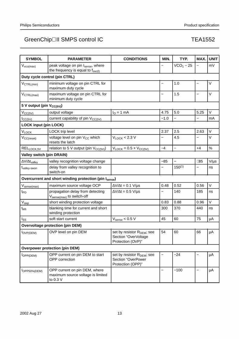
2002 Aug 27 13
Philips Semiconductors Product specification
GreenChipII SMPS control IC TEA1552
Vvco(max) peak voltage on pin Isense, wherethe frequency is equal to fosc(l)
− VCO1 − 25 − mV
Duty cycle control (pin CTRL)
VCTRL(min) minimum voltage on pin CTRL formaximum duty cycle
− 1.0 − V
VCTRL(max) maximum voltage on pin CTRL forminimum duty cycle
− 1.5 − V
5 V output (pin V CC(5V))
VCC(5V) output voltage IO = 1 mA 4.75 5.0 5.25 V
ICC(5V) current capability of pin VCC(5V) −1.0 − − mA
LOCK input (pin LOCK)
VLOCK LOCK trip level 2.37 2.5 2.63 V
VCC(reset) voltage level on pin VCC whichresets the latch
VLOCK < 2.3 V − 4.5 − V
RELLOCK,5V relation to 5 V output (pin VCC(5V)) VLOCK = 0.5 × VCC(5V) −4 − +4 %
Valley switch (pin DRAIN)
∆V/∆tvalley valley recognition voltage change −85 − +85 V/µs
tvalley-swon delay from valley recognition toswitch-on
− 150(1) − ns
Overcurrent and short winding protection (pin I sense )
Vsense(max) maximum source voltage OCP ∆V/∆t = 0.1 V/µs 0.48 0.52 0.56 V
tPD propagation delay from detectingVsense(max) to switch-off
∆V/∆t = 0.5 V/µs − 140 185 ns
Vswp short winding protection voltage 0.83 0.88 0.96 V
tleb blanking time for current and shortwinding protection
300 370 440 ns
ISS soft start current Vsense < 0.5 V 45 60 75 µA
Overvoltage protection (pin DEM)
IOVP(DEM) OVP level on pin DEM set by resistor RDEM; seeSection “OverVoltageProtection (OVP)”
54 60 66 µA
Overpower protection (pin DEM)
IOPP(DEM) OPP current on pin DEM to startOPP correction
set by resistor RDEM; seeSection “OverPowerProtection (OPP)”
− −24 − µA
IOPP50%(DEM) OPP current on pin DEM, wheremaximum source voltage is limitedto 0.3 V
− −100 − µA
SYMBOL PARAMETER CONDITIONS MIN. TYP. MAX. UNIT

2002 Aug 27 14
Philips Semiconductors Product specification
GreenChipII SMPS control IC TEA1552
Note
1. Guaranteed by design.
Standby output (pin STDBY)
VSTDBY standby output voltage 4.75 5.0 5.25 V
Isource source current capability VSTDBY = 1 V 20 22 24 µA
Isink sink current capability VSTDBY = 1 V 2 − − mA
Driver (pin DRIVER)
Isource source current capability of driver VCC = 9.5 V; VDRIVER = 2 V − −170 −88 mA
Isink sink current capability of driver VCC = 9.5 V; VDRIVER = 2 V − 300 − mA
VCC = 9.5 V;VDRIVER = 9.5 V
400 700 − mA
Vo(driver)(max) maximum output voltage of driver VCC > 12 V − 11.5 12 V
Temperature protection
Tprot(max) maximum temperature protectionlevel
130 140 150 °C
Tprot(hys) hysteresis for the temperatureprotection level
− 8(1) − °C
SYMBOL PARAMETER CONDITIONS MIN. TYP. MAX. UNIT

2002 Aug 27 15
Philips Semiconductors Product specification
GreenChipII SMPS control IC TEA1552
APPLICATION INFORMATION
A converter with the TEA1552 consists of an input filter, a transformer with a third winding (auxiliary), and an output stagewith a feedback circuit.
Capacitor CVCC (at pin VCC) buffers the supply voltage of the IC, which is powered via the high voltage rectified mainsduring start-up and via the auxiliary winding during operation.
A sense resistor converts the primary current into a voltage at pin Isense. The value of this sense resistor defines themaximum primary peak current.
handbook, full pagewidth
MBL504
TEA1552T
1
2
3
4
5
6
7
14
13
12
11
10
9
8
VCOadj
Isense
STDBY
DRIVER
HVS
HVS
DRAIN
PFC
DEM
CTRL
LOCK
−t
VCC(5V)
GND
n.c.
VCC
RSS
RDEM
RCTRL
CCTRL
Rs2
CSS
Naux
Rsense
Rreg1
Rreg2
powerMOSFET
Np
CVCC
Ns
Vi
Vmains
Vo
Co
Do
Fig.11 Configuration with controlled PFC.
The LOCK pin is used in this example for an additional external overtemperature protection.If this pin is not used, it must be tied to ground.
2002 Aug 27 16
Philips Semiconductors Product specification
GreenChipII SMPS control IC TEA1552
handbook, full pagewidth
VµC
start-upsequence
normaloperation
normaloperation
overvoltageprotection
outputshort-circuit
MBL505
Vi
Vo
VD(power
MOSFET)
VCC
M-level
Vgate
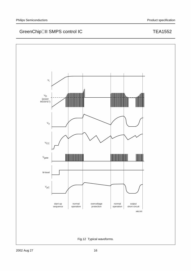
Fig.12 Typical waveforms.
2002 Aug 27 17
Philips Semiconductors Product specification
GreenChipII SMPS control IC TEA1552
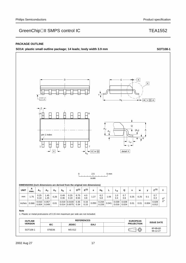
PACKAGE OUTLINE
UNITA
max. A1 A2 A3 bp c D(1) E(1) (1)e HE L Lp Q Zywv θ
REFERENCESOUTLINEVERSION
EUROPEANPROJECTION ISSUE DATE
IEC JEDEC EIAJ
mm
inches
1.750.250.10
1.451.25 0.25
0.490.36
0.250.19
8.758.55
4.03.8
1.276.25.8
0.70.6
0.70.3 8
0
o
o
0.25 0.1
DIMENSIONS (inch dimensions are derived from the original mm dimensions)
Note
1. Plastic or metal protrusions of 0.15 mm maximum per side are not included.
1.00.4
SOT108-1
X
w M
θ
AA1
A2
bp
D
HE
Lp
Q
detail X
E
Z
e
c
L
v M A
(A )3
A
7
8
1
14
y
076E06 MS-012
pin 1 index
0.0690.0100.004
0.0570.049 0.01
0.0190.014
0.01000.0075
0.350.34
0.160.15
0.050
1.05
0.0410.2440.228
0.0280.024
0.0280.0120.01
0.25
0.01 0.0040.0390.016
97-05-2299-12-27
0 2.5 5 mm
scale
SO14: plastic small outline package; 14 leads; body width 3.9 mm SOT108-1
2002 Aug 27 18
Philips Semiconductors Product specification
GreenChipII SMPS control IC TEA1552
SOLDERING
Introduction to soldering surface mount packages
This text gives a very brief insight to a complex technology.A more in-depth account of soldering ICs can be found inour “Data Handbook IC26; Integrated Circuit Packages”(document order number 9398 652 90011).
There is no soldering method that is ideal for all surfacemount IC packages. Wave soldering can still be used forcertain surface mount ICs, but it is not suitable for fine pitchSMDs. In these situations reflow soldering isrecommended.
Reflow soldering
Reflow soldering requires solder paste (a suspension offine solder particles, flux and binding agent) to be appliedto the printed-circuit board by screen printing, stencilling orpressure-syringe dispensing before package placement.
Several methods exist for reflowing; for example,convection or convection/infrared heating in a conveyortype oven. Throughput times (preheating, soldering andcooling) vary between 100 and 200 seconds dependingon heating method.
Typical reflow peak temperatures range from215 to 250 °C. The top-surface temperature of thepackages should preferable be kept below 220 °C forthick/large packages, and below 235 °C for small/thinpackages.
Wave soldering
Conventional single wave soldering is not recommendedfor surface mount devices (SMDs) or printed-circuit boardswith a high component density, as solder bridging andnon-wetting can present major problems.
To overcome these problems the double-wave solderingmethod was specifically developed.
If wave soldering is used the following conditions must beobserved for optimal results:
• Use a double-wave soldering method comprising aturbulent wave with high upward pressure followed by asmooth laminar wave.
• For packages with leads on two sides and a pitch (e):
– larger than or equal to 1.27 mm, the footprintlongitudinal axis is preferred to be parallel to thetransport direction of the printed-circuit board;
– smaller than 1.27 mm, the footprint longitudinal axismust be parallel to the transport direction of theprinted-circuit board.
The footprint must incorporate solder thieves at thedownstream end.
• For packages with leads on four sides, the footprint mustbe placed at a 45° angle to the transport direction of theprinted-circuit board. The footprint must incorporatesolder thieves downstream and at the side corners.
During placement and before soldering, the package mustbe fixed with a droplet of adhesive. The adhesive can beapplied by screen printing, pin transfer or syringedispensing. The package can be soldered after theadhesive is cured.
Typical dwell time is 4 seconds at 250 °C.A mildly-activated flux will eliminate the need for removalof corrosive residues in most applications.
Manual soldering
Fix the component by first soldering twodiagonally-opposite end leads. Use a low voltage (24 V orless) soldering iron applied to the flat part of the lead.Contact time must be limited to 10 seconds at up to300 °C.
When using a dedicated tool, all other leads can besoldered in one operation within 2 to 5 seconds between270 and 320 °C.

2002 Aug 27 19
Philips Semiconductors Product specification
GreenChipII SMPS control IC TEA1552
Suitability of surface mount IC packages for wave and reflow soldering methods
Notes
1. For more detailed information on the BGA packages refer to the “(LF)BGA Application Note” (AN01026); order a copyfrom your Philips Semiconductors sales office.
2. All surface mount (SMD) packages are moisture sensitive. Depending upon the moisture content, the maximumtemperature (with respect to time) and body size of the package, there is a risk that internal or external packagecracks may occur due to vaporization of the moisture in them (the so called popcorn effect). For details, refer to theDrypack information in the “Data Handbook IC26; Integrated Circuit Packages; Section: Packing Methods”.
3. These packages are not suitable for wave soldering. On versions with the heatsink on the bottom side, the soldercannot penetrate between the printed-circuit board and the heatsink. On versions with the heatsink on the top side,the solder might be deposited on the heatsink surface.
4. If wave soldering is considered, then the package must be placed at a 45° angle to the solder wave direction.The package footprint must incorporate solder thieves downstream and at the side corners.
5. Wave soldering is suitable for LQFP, TQFP and QFP packages with a pitch (e) larger than 0.8 mm; it is definitely notsuitable for packages with a pitch (e) equal to or smaller than 0.65 mm.
6. Wave soldering is suitable for SSOP and TSSOP packages with a pitch (e) equal to or larger than 0.65 mm; it isdefinitely not suitable for packages with a pitch (e) equal to or smaller than 0.5 mm.
PACKAGE (1)SOLDERING METHOD
WAVE REFLOW (2)
BGA, LBGA, LFBGA, SQFP, TFBGA, VFBGA not suitable suitable
HBCC, HBGA, HLQFP, HSQFP, HSOP, HTQFP, HTSSOP, HVQFN,HVSON, SMS
not suitable(3) suitable
PLCC(4), SO, SOJ suitable suitable
LQFP, QFP, TQFP not recommended(4)(5) suitable
SSOP, TSSOP, VSO not recommended(6) suitable

2002 Aug 27 20
Philips Semiconductors Product specification
GreenChipII SMPS control IC TEA1552
DATA SHEET STATUS
Notes
1. Please consult the most recently issued data sheet before initiating or completing a design.
2. The product status of the device(s) described in this data sheet may have changed since this data sheet waspublished. The latest information is available on the Internet at URL http://www.semiconductors.philips.com.
DATA SHEET STATUS (1) PRODUCTSTATUS(2) DEFINITIONS
Objective data Development This data sheet contains data from the objective specification for productdevelopment. Philips Semiconductors reserves the right to change thespecification in any manner without notice.
Preliminary data Qualification This data sheet contains data from the preliminary specification.Supplementary data will be published at a later date. PhilipsSemiconductors reserves the right to change the specification withoutnotice, in order to improve the design and supply the best possibleproduct.
Product data Production This data sheet contains data from the product specification. PhilipsSemiconductors reserves the right to make changes at any time in orderto improve the design, manufacturing and supply. Changes will becommunicated according to the Customer Product/Process ChangeNotification (CPCN) procedure SNW-SQ-650A.
DEFINITIONS
Short-form specification The data in a short-formspecification is extracted from a full data sheet with thesame type number and title. For detailed information seethe relevant data sheet or data handbook.
Limiting values definition Limiting values given are inaccordance with the Absolute Maximum Rating System(IEC 60134). Stress above one or more of the limitingvalues may cause permanent damage to the device.These are stress ratings only and operation of the deviceat these or at any other conditions above those given in theCharacteristics sections of the specification is not implied.Exposure to limiting values for extended periods mayaffect device reliability.
Application information Applications that aredescribed herein for any of these products are forillustrative purposes only. Philips Semiconductors makeno representation or warranty that such applications will besuitable for the specified use without further testing ormodification.
DISCLAIMERS
Life support applications These products are notdesigned for use in life support appliances, devices, orsystems where malfunction of these products canreasonably be expected to result in personal injury. PhilipsSemiconductors customers using or selling these productsfor use in such applications do so at their own risk andagree to fully indemnify Philips Semiconductors for anydamages resulting from such application.
Right to make changes Philips Semiconductorsreserves the right to make changes, without notice, in theproducts, including circuits, standard cells, and/orsoftware, described or contained herein in order toimprove design and/or performance. PhilipsSemiconductors assumes no responsibility or liability forthe use of any of these products, conveys no licence or titleunder any patent, copyright, or mask work right to theseproducts, and makes no representations or warranties thatthese products are free from patent, copyright, or maskwork right infringement, unless otherwise specified.

2002 Aug 27 21
Philips Semiconductors Product specification
GreenChipII SMPS control IC TEA1552
NOTES

2002 Aug 27 22
Philips Semiconductors Product specification
GreenChipII SMPS control IC TEA1552
NOTES

2002 Aug 27 23
Philips Semiconductors Product specification
GreenChipII SMPS control IC TEA1552
NOTES

© Koninklijke Philips Electronics N.V. 2002 SCA74All rights are reserved. Reproduction in whole or in part is prohibited without the prior written consent of the copyright owner.
The information presented in this document does not form part of any quotation or contract, is believed to be accurate and reliable and may be changedwithout notice. No liability will be accepted by the publisher for any consequence of its use. Publication thereof does not convey nor imply any licenseunder patent- or other industrial or intellectual property rights.
Philips Semiconductors – a worldwide company
Contact information
For additional information please visit http://www.semiconductors.philips.com . Fax: +31 40 27 24825For sales offices addresses send e-mail to: [email protected] .
Printed in The Netherlands 613502/02/pp24 Date of release: 2002 Aug 27 Document order number: 9397 750 10259