Embed Size (px)
Citation preview
TEAC 22” TFT IDTV
SERVICE MANUAL
i 22” TFT TV Service Manual 13/10/2004
TABLE OF CONTENTS
1. INTRODUCTION ...................................................................................................................................... 1 2. TUNER...................................................................................................................................................... 1 3. IF PART (TDA988X) ................................................................................................................................. 1 4. MULTI STANDARD SOUND PROCESSOR............................................................................................ 1 5. AUDIO AMPLIFIER STAGE WITH AN7522............................................................................................. 2 6. POWER .................................................................................................................................................... 2 7. MICROCONTROLLER SDA55XX............................................................................................................ 2
7.1. General Features .................................................................................................................................. 2 7.2. External Crystal and Programmable Clock Speed ............................................................................... 2 7.3. Microcontroller Features ....................................................................................................................... 2 7.4. Memory ................................................................................................................................................. 2 7.5. Display Features ................................................................................................................................... 2 7.6. ROM Characters ................................................................................................................................... 3 7.7. Acquisition Features.............................................................................................................................. 3 7.8. Ports...................................................................................................................................................... 3
8. SERIAL ACCESS CMOS 16K (2048*8) EEPROM ST24C16.................................................................. 3 9. CLASS AB STEREO HEADPHONE DRIVER TDA1308 ......................................................................... 3 10. SAW FILTERS.......................................................................................................................................... 3 11. IC DESCRIPTIONS (FOR ANALOG) ....................................................................................................... 4
11.1. LM1117.............................................................................................................................................. 4 11.1.1. General Description ................................................................................................................. 4 11.1.2. Features .................................................................................................................................... 4 11.1.3. Applications.............................................................................................................................. 4 11.1.4. Connection Diagrams .............................................................................................................. 4
11.2. LM2576.............................................................................................................................................. 5 11.2.1. General Description ................................................................................................................. 5 11.2.2. Features .................................................................................................................................... 5 11.2.3. Pin description ......................................................................................................................... 5
11.3. LM317T ............................................................................................................................................. 6 11.3.1. Description................................................................................................................................ 6 11.3.2. Features .................................................................................................................................... 6
11.4. TFMS5360......................................................................................................................................... 6 11.4.1. Description................................................................................................................................ 6 11.4.2. Features .................................................................................................................................... 6
11.5. ST24LC21 ......................................................................................................................................... 7 11.5.1. Description................................................................................................................................ 7 11.5.2. Features .................................................................................................................................... 7 11.5.3. Pin connections........................................................................................................................ 7
11.6. SST37VF040 ..................................................................................................................................... 8 11.6.1. Description................................................................................................................................ 8 11.6.2. Features .................................................................................................................................... 8 11.6.3. Pin Description ......................................................................................................................... 8
11.7. TEA5114A ......................................................................................................................................... 9 11.7.1. General description ................................................................................................................. 9 11.7.2. Features .................................................................................................................................... 9 11.7.3. Pin Connections ....................................................................................................................... 9
11.8. TEA6415.......................................................................................................................................... 10 11.8.1. General description ............................................................................................................... 10 11.8.2. 13.5.2.Features ....................................................................................................................... 10 11.8.3. 13.5.3.Pinning ......................................................................................................................... 10
11.9. VPC3230D....................................................................................................................................... 11 11.9.1. General Description ............................................................................................................... 11 11.9.2. Pin Connections and Short Descriptions ............................................................................ 11
11.10. SDA55XX (SDA5550)...................................................................................................................... 13 11.10.1. General description ............................................................................................................... 13
11.11. TDA9885/86 .................................................................................................................................... 14 11.11.1. General description ............................................................................................................... 14
ii 22” TFT TV Service Manual 13/10/2004
11.11.2. Features .................................................................................................................................. 14 11.11.3. Pinning .................................................................................................................................... 14
11.12. TDA1308 ......................................................................................................................................... 15 11.12.1. General Description ............................................................................................................... 15 11.12.2. Features .................................................................................................................................. 15 11.12.3. Pinning .................................................................................................................................... 15
11.13. AN7522N ......................................................................................................................................... 15 11.13.1. General description ............................................................................................................... 15 11.13.2. Pin Descriptions ..................................................................................................................... 15
11.14. PI5V330........................................................................................................................................... 16 11.14.1. General description ............................................................................................................... 16 11.14.2. Features .................................................................................................................................. 16 11.14.3. Pin Descriptions ..................................................................................................................... 16
11.15. GM6015........................................................................................................................................... 17 11.15.1. General description ............................................................................................................... 17 11.15.2. Features .................................................................................................................................. 17
11.16. SAA3010T ....................................................................................................................................... 18 11.16.1. Description.............................................................................................................................. 18 11.16.2. Features .................................................................................................................................. 18 11.16.3. Pinning .................................................................................................................................... 18
11.17. AD9883A ......................................................................................................................................... 19 11.17.1. General description ............................................................................................................... 19 11.17.2. Features .................................................................................................................................. 19 11.17.3. Pin Descriptions ..................................................................................................................... 19
11.18. MC141585 ....................................................................................................................................... 22 11.18.1. General description ............................................................................................................... 22 11.18.2. Features .................................................................................................................................. 22 11.18.3. Pin Description ....................................................................................................................... 22
11.19. MC34063 ......................................................................................................................................... 24 11.19.1. Description.............................................................................................................................. 24 11.19.2. Features .................................................................................................................................. 24 11.19.3. Pin connections...................................................................................................................... 24
11.20. MSP34X0G...................................................................................................................................... 25 11.20.1. Introduction ............................................................................................................................ 25 11.20.2. Features .................................................................................................................................. 25 11.20.3. Pin connections...................................................................................................................... 26
11.21. DS90C385 ....................................................................................................................................... 28 11.21.1. General Description ............................................................................................................... 28 11.21.2. Features .................................................................................................................................. 28 11.21.3. Pin Descriptions ..................................................................................................................... 28
11.22. 4053B .............................................................................................................................................. 31 11.22.1. General Description ............................................................................................................... 31 11.22.2. Pin Description ....................................................................................................................... 31
11.23. 24C16 .............................................................................................................................................. 32 11.23.1. General Description ............................................................................................................... 32 11.23.2. Features .................................................................................................................................. 32 11.23.3. Pin Description ....................................................................................................................... 32
11.24. 74LX1G86STR ................................................................................................................................ 33 11.24.1. General Description ............................................................................................................... 33 11.24.2. Features .................................................................................................................................. 33 11.24.3. Pin Description ....................................................................................................................... 33
11.25. IRF7314........................................................................................................................................... 34 11.25.1. General Description ............................................................................................................... 34 11.25.2. Features .................................................................................................................................. 34 11.25.3. Pin Description ....................................................................................................................... 34
12. IC DESCRIPTIONS (FOR DIGITAL) ...................................................................................................... 35 12.1. STI5518 ........................................................................................................................................... 35
12.1.1. General Description ............................................................................................................... 35 12.2. MAX232_SMD................................................................................................................................. 35
12.2.1. General Description ............................................................................................................... 35
iii 22” TFT TV Service Manual 13/10/2004
12.2.2. Features .................................................................................................................................. 35 12.3. 74HCU04......................................................................................................................................... 36
12.3.1. General Description ............................................................................................................... 36 12.3.2. Pin Description ....................................................................................................................... 36
12.4. TSH22 ............................................................................................................................................. 37 12.4.1. General Description ............................................................................................................... 37 12.4.2. Pin Connections ..................................................................................................................... 37
12.5. CS4334............................................................................................................................................ 37 12.5.1. General Description ............................................................................................................... 37 12.5.2. Features .................................................................................................................................. 37
12.6. AMIC A43L2616 .............................................................................................................................. 38 12.6.1. General Description ............................................................................................................... 38 12.6.2. Features .................................................................................................................................. 38 12.6.3. Pin Description ....................................................................................................................... 38
12.7. MX29LV160T................................................................................................................................... 40 12.7.1. General Description ............................................................................................................... 40 12.7.2. Features .................................................................................................................................. 40 12.7.3. Pin Description ....................................................................................................................... 40
12.8. 24C32 .............................................................................................................................................. 41 12.8.1. General Description ............................................................................................................... 41 12.8.2. Features .................................................................................................................................. 41 12.8.3. Pin Description ....................................................................................................................... 41
12.9. STV0360.......................................................................................................................................... 42 12.9.1. General Description ............................................................................................................... 42 12.9.2. Features .................................................................................................................................. 42 12.9.3. Pin Description ....................................................................................................................... 42
12.10. MAX809........................................................................................................................................... 45 12.10.1. General Description ............................................................................................................... 45 12.10.2. Features .................................................................................................................................. 45 12.10.3. Pin Description ....................................................................................................................... 45
12.11. TDCC2345TV39A............................................................................................................................ 46 12.11.1. General Description ............................................................................................................... 46 12.11.2. Pin Description ....................................................................................................................... 46
13. SERVICE MENU SETTINGS ................................................................................................................. 47 13.1. ADJUST MENU SETTINGS............................................................................................................ 47 13.2. OPTIONS MENU SETTINGS..........................................................................................................48 13.3. APS WSS TEST MENU .................................................................................................................. 53
14. BLOCK DIAGRAMS ............................................................................................................................... 54 14.1. ANALOG.......................................................................................................................................... 54 14.2. DIGITAL........................................................................................................................................... 58
15. CIRCUIT DIAGRAMS............................................................................................................................. 59 15.1. ANALOG.......................................................................................................................................... 59 15.2. DIGITAL........................................................................................................................................... 68
1 22” TFT TV Service Manual 13/10/2004
1. INTRODUCTION 22” TFT-LCD IDTV is a Progressive TV control system based on the µ-controller SDA555X, with built-in de-interlacer and scaler. It is designed to deliver digital quality pictures without the need of a separate digital terrestrial receiver. TFT IDTV is a progressive scan flicker free colour television with PC input, driving an WXGA (1280*720) panel with 16:9 aspect ratio. The chassis is capable of operation in PAL, SECAM, NTSC (playback) colour standards and multiple transmission standards as B/G, D/K, I/I’, and L/L´. Sound system output is supplying 2x3W (10%THD) for left and right outputs of 16Ω speakers. The chassis is equipped with two full SCART’s, one front-AV, one SVHS, one D-Sub 15 (PC) input, one PC stereo audio input and one line out (left and right) and one HP outputs. 2. TUNER As the thickness of the TV set has a limit, a horizontal mounted tuner is used in the product, which is suitable for CCIR systems B/G, H, L, L´, I/I´, and D/K. The tuning is available through the digitally controlled I2C bus (PLL). Below you will find info on the Tuner in use. General description of UV1316: The UV1316 tuner belongs to the UV 1300 family of tuners, which are designed to meet a wide range of applications. It is a combined VHF, UHF tuner suitable for CCIR systems B/G, H, L, L’, I and I’. The low IF output impedance has been designed for direct drive of a wide variety of SAW filters with sufficient suppression of triple transient. Features of UV1316: 1. Member of the UV1300 family small sized UHF/VHF tuners 2. Systems CCIR: B/G, H, L, L’, I and I’; OIRT: D/K 3. Digitally controlled (PLL) tuning via I2C-bus 4. Off-air channels, S-cable channels and Hyper band 5. Compact size 6. Complies to “CENELEC EN55020” and “EN55013” Pinning: 1. Gain control voltage (AGC) : 4.0V, Max: 4.5V 2. Tuning voltage 3. I²C-bus address select : Max: 5.5V 4. I²C-bus serial clock : Min:-0.3V, Max: 5.5V 5. I²C-bus serial data : Min:-0.3V, Max: 5.5V 6. Not connected 7. PLL supply voltage : 5.0V, Min: 4.75V, Max: 5.5V 8. ADC input 9. Tuner supply voltage : 33V, Min: 30V, Max: 35V 10. Symmetrical IF output 1 11. Symmetrical IF output 2 3. IF PART (TDA988X) The TDA9885 is an alignment-free single standard (without positive modulation) vision and sound IF signal PLL. The TDA9886 is an alignment-free multistandard (PAL, SECAM and NTSC) vision and sound IF signal PLL demodulator for positive and negative modulation including sound AM and FM processing. Both devices can be used for TV, VTR, PC and set-top box applications. 4. MULTI STANDARD SOUND PROCESSOR The MSP34x0G family of single-chip Multistandard Sound Processors covers the sound processing of all analog TV-Standards worldwide, as well as the NICAM digital sound standards. The full TV sound processing, starting with analog sound IF signal-in, down to processed analog AF-out, is performed on a single chip. These TV sound processing ICs include versions for processing the multichannel television sound (MTS) signal conforming to the standard recommended by the Broadcast Television Systems Committee (BTSC). The DBX noise reduction, or alternatively, Micronas Noise Reduction (MNR) is performed alignment free. Other processed standards are the Japanese FM-FM multiplex standard (EIA-J) and the FM Stereo Radio standard. Current ICs have to perform adjustment procedures in order to achieve good stereo separation for BTSC and EIA-J. The MSP 34x1G has optimum stereo performance without any adjustments.
2 22” TFT TV Service Manual 13/10/2004
5. AUDIO AMPLIFIER STAGE WITH AN7522 The AN7522 is an audio class-AB amplifier assembled in SIL-12 Pin Plastic Package specially designed for sound cards application. Using this IC chassis operates as a stereo TV set. AN7522 has stand-by feature for low stand-by power consumption and mute feature for pop noise free opening and closing the TV set. It can deliver 2*3W without clipping at 12V/16Ω applications. 6. POWER The LM2576 series of regulators are monolithic integrated circuits ideally suited for easy and convenient design of a step–down switching regulator (buck converter). All circuits of this series are capable of driving a 3.0A load with excellent line and load regulation. Two different versions (one having a fixed output voltage of 3.3 V, and one with 5.0 V) of this IC are used in the regulator board. 7. MICROCONTROLLER SDA55XX
7.1. General Features • Feature selection via special function register • Simultaneous reception of TTX, VPS, PDC, and WSS (line 23) • Supply Voltage 2.5 and 3.3 V • ROM version is used.
7.2. External Crystal and Programmable Clock Speed • Single external 6MHz crystal, all necessary clocks are generated internally • CPU clock speed selectable via special function registers. • Normal Mode 33.33 MHz CPU clock, Power Save mode 8.33 MHz
7.3. Microcontroller Features • 8bit 8051 instruction set compatible CPU. • 33.33-MHz internal clock (max.) • 0.360 µs (min.) instruction cycle • Two 16-bit timers • Watchdog timer • Capture compare timer for infrared remote control decoding • Pulse width modulation unit (2 channels 14 bit, 6 channels 8 bit) • ADC (4 channels, 8 bit) • UART (rxd, txd)
7.4. Memory • Up to 128 Kilobyte on Chip Program ROM • Eight 16-bit data pointer registers (DPTR) • 256-bytes on-chip Processor Internal RAM (IRAM) • 128bytes extended stack memory. • Display RAM and TXT/VPS/PDC/WSS-Acquisition-Buffer directly accessible via MOVX • UP to 16KByte on Chip Extended RAM (XRAM) consisting of; - 1 Kilobyte on-chip ACQ-buffer-RAM (access via MOVX) - 1 Kilobyte on-chip extended-RAM (XRAM, access via MOVX) for user software - 3-Kilobyte Display Memory
7.5. Display Features • ROM Character set supports all East and West European Languages in single device • Mosaic Graphic Character Set • Parallel Display Attributes • Single/Double Width/Height of Characters • Variable Flash Rate • Programmable Screen Size (25 Rows x 33...64 Columns) • Flexible Character Matrixes (HxV) 12 x 9...16 • Up to 256 Dynamical Redefinable Characters in standard mode; 1024 Dynamical Redefinable Characters in Enhanced Mode • CLUT with up to 4096 colour combinations • Up to 16 Colours per DRCS Character • One out of 8 Colours for Foreground and Background Colours for 1-bit DRCS and ROM Characters
3 22” TFT TV Service Manual 13/10/2004
7.6. ROM Characters • Shadowing • Contrast Reduction • Pixel by Pixel Shiftable Cursor With up to 4 Different Colours • Support of Progressive Scan and 100 Hz. • 3 X 4Bits RGB-DACs On-Chip • Free Programmable Pixel Clock from 10 MHz to 32MHz • Pixel Clock Independent from CPU Clock • Multinorm H/V-Display Synchronisation in Master or Slave Mode
7.7. Acquisition Features • Multistandard Digital Data Slicer • Parallel Multi-norm Slicing (TTX, VPS, WSS, CC, G+) • Four Different Framing Codes Available • Data Caption only limited by available Memory • Programmable VBI-buffer • Full Channel Data Slicing Supported • Fully Digital Signal Processing • Noise Measurement and Controlled Noise Compensation • Attenuation Measurement and Compensation • Group Delay Measurement and Compensation • Exact Decoding of Echo Disturbed Signals
7.8. Ports • One 8-bit I/O-port with open drain output and optional I 2 C Bus emulation support (Port0) • Two 8-bit multifunction I/O-ports (Port1, Port3) • One 4-bit port working as digital or analogue inputs for the ADC (Port2) • One 2-bit I/O port with secondary function (P4.2, 4.3, 4.7) • One 4-bit I/O-port with secondary function (P4.0, 4.1, 4.4) (Not available in P-SDIP 52) 8. SERIAL ACCESS CMOS 16K (2048*8) EEPROM ST24C16 The ST24C16 is a 16Kbit electrically erasable programmable memory (EEPROM), organised as 8 blocks of 256*8 bits. The memory is compatible with the I²C standard, two wire serial interface, which uses a bi-directional data bus and serial clock. The memory carries a built-in 4 bit, unique device identification code (1010) corresponding to the I²C bus definition. This is used together with 1 chip enable input (E) so that up to 2*8K devices may be attached to the I²C bus and selected individually. 9. CLASS AB STEREO HEADPHONE DRIVER TDA1308 The TDA1308 is an integrated class AB stereo headphone driver contained in a DIP8 plastic package. The device is fabricated in a 1 mm CMOS process and has been primarily developed for portable digital audio applications. 10. SAW FILTERS K3953M is an IF Filter for Video Applications. The package is SIP5K. Supported standards are B/G, D/K, I, L/L’. K9656M is an IF Filter for Audio Applications. The package is SIP5K. Supported standards are B/G, D/K, I, L/L’.
4 22” TFT TV Service Manual 13/10/2004
11. IC DESCRIPTIONS (FOR ANALOG)
LM1117 PI5V330 LM2576 GM6015 LM317T SAA3010T
TFMS5360 AD9883A ST24LC21 MC141585
SST37VF040 MC34063 TEA5114A MSP3410G TEA6415 DS90C385
VPC3230D 4053B SDA55XX 24C16
TDA9885/86 74LX1G86STR TDA1308T IRF7314 AN7522N
11.1. LM1117
11.1.1. General Description The LM1117 is a series of low dropout voltage regulators with a dropout of 1.2V at 800mA of load current. It has the same pin-out as National Semiconductor’s industry standard LM317. The LM1117 is available in an adjustable version, which can set the output voltage from 1.25V to 13.8V with only two external resistors. In addition, it is also available in five fixed voltages, 1.8V, 2.5V, 2.85V, 3.3V, and 5V. The LM1117 offers current limiting and thermal shutdown. Its circuit includes a zener trimmed bandgap reference to as-sure output voltage accuracy to within ±1%. The LM1117 series is available in SOT-223, TO-220, and TO-252 D-PAK packages. A minimum of 10µF tantalum capacitor is required at the output to improve the transient response and stability.
11.1.2. Features • Available in 1.8V, 2.5V, 2.85V, 3.3V, 5V, and Adjustable Versions • Space Saving SOT-223 Package • Current Limiting and Thermal Protection • Output Current 800mA • Line Regulation 0.2% (Max) • Load Regulation 0.4% (Max) • Temperature Range LM1117 0°C to 125°C LM1117I -40°C to 125°C
11.1.3. Applications • 2.85V Model for SCSI-2 Active Termination • Post Regulator for Switching DC/DC Converter • High Efficiency Linear Regulators • Battery Charger • Battery Powered Instrumentation
11.1.4. Connection Diagrams
5 22” TFT TV Service Manual 13/10/2004
11.2. LM2576
11.2.1. General Description The LM2576 series of regulators are monolithic integrated circuits ideally suited for easy and convenient design of a step–down switching regulator (buck converter). All circuits of this series are capable of driving a 3.0 A load with excellent line and load regulation. These devices are available in fixed output voltages of 3.3 V, 5.0 V, 12 V, 15 V, and an adjustable output version. These regulators were designed to minimize the number of external components to simplify the power supply design. Standard series of inductors optimized for use with the LM2576 are offered by several different inductor manufacturers. Since the LM2576 converter is a switch–mode power supply, its efficiency is significantly higher in comparison with popular three–terminal linear regulators, especially with higher input voltages. In many cases, the power dissipated is so low that no heatsink is required or its size could be reduced dramatically. A standard series of inductors optimized for use with the LM2576 are available from several different manufacturers. This feature greatly simplifies the design of switch–mode power supplies. The LM2576 features include a guaranteed ±4% tolerance on output voltage within specified input voltages and output load conditions, and ±10% on the oscillator frequency (±2% over 0°C to 125°C). External shutdown is included, featuring 80 mA (typical) standby current. The output switch includes cycle–by–cycle current limiting, as well as thermal shutdown for full protection under fault conditions.
11.2.2. Features • 3.3 V, 5.0 V, 12 V, 15 V, and Adjustable Output Versions • Adjustable Version Output Voltage Range, 1.23 to 37 V ±4% Maximum Over Line and Load Conditions • Guaranteed 3.0 A Output Current • Wide Input Voltage Range • Requires Only 4 External Components • 52 kHz Fixed Frequency Internal Oscillator • TTL Shutdown Capability, Low Power Standby Mode • High Efficiency • Uses Readily Available Standard Inductors • Thermal Shutdown and Current Limit Protection • Moisture Sensitivity Level (MSL) Equals 1
11.2.3. Pin description
6 22” TFT TV Service Manual 13/10/2004
11.3. LM317T
11.3.1. Description The LM317T is an adjustable 3 terminal positive voltage regulator capable of supplying in excess of 1.5 amps over an output range of 1.25 to 37 volts. This voltage regulator is exceptionally easy to use and requires only two external resistors to set the output voltage. Further, it employs internal current limiting, thermal shutdown and safe area compensation, making it essentially blow–out proof. The LM317 serves a wide variety of applications including local, on card regulation. This device can also be used to make a programmable output regulator, or by connecting a fixed resistor between the adjustment and output, the LM317 can be used as a precision current regulator.
11.3.2. Features • Output Current in Excess of 1.5 A • Output Adjustable between 1.2 V and 37 V • Internal Thermal Overload Protection • Internal Short Circuit Current Limiting Constant with Temperature • Output Transistor Safe–Area Compensation • Floating Operation for High Voltage Applications • Available in Surface Mount D2PAK, and Standard 3–Lead Transistor Package • Eliminates Stocking many Fixed Voltages
11.4. TFMS5360
11.4.1. Description The TFMS5360 is a miniature receiver for infrared remote control systems.
11.4.2. Features • Photo detector and preamplifier in one. • 36 KHZ • Pin diode and preamp • IR filter.
7 22” TFT TV Service Manual 13/10/2004
11.5. ST24LC21
11.5.1. Description The ST24LC21 is a 1K bit electrically erasable programmable memory (EEPROM), organized by 8 bits. This device can operate in two modes: Transmit Only mode and I2C bidirectional mode. When powered, the device is in Transmit Only mode with EEPROM data clocked out from the rising edge of the signal applied on VCLK. The device will switch to the I2C bidirectional mode upon the falling edge of the signal applied on SCL pin. The ST24LC21 can not switch from the I2C bidirectional mode to the Transmit Only mode (except when the power supply is removed). The device operates with a power supply value as low as 2.5V. Both Plastic Dual-in-Line and Plastic Small Outline packages are available.
11.5.2. Features • 1 million Erase/Write cycles • 40 years data retention • 2.5V to 5.5V single supply voltage • 400k Hz compatibility over the full range of supply voltage • Two wire serial interface I2C bus compatible • Page Write (Up To 8 Bytes) • Byte, random and sequential read modes • Self timed programming cycle • Automatic address incrementing • Enhanced ESD/Latch up • Performances
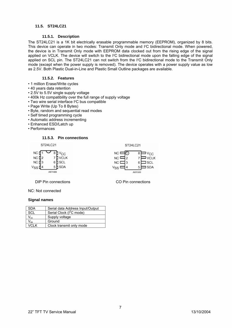
11.5.3. Pin connections
DIP Pin connections CO Pin connections NC: Not connected Signal names SDA Serial data Address Input/Output SCL Serial Clock (I2C mode) Vcc Supply voltage Vss Ground VCLK Clock transmit only mode
8 22” TFT TV Service Manual 13/10/2004
11.6. SST37VF040
11.6.1. Description The SST37VF512/010/020/040 devices are 64K x8 / 128Kx8 / 256K x8 / 512K x8 CMOS, Many-Time Programmable (MTP), low cost flash, manufactured with SST’s proprietary, high performance CMOS Super Flash technology. The split-gate cell design and thick oxide tunneling injector attain better reliability and manufacturability compared with alternate approaches. The SST37VF512/010/020/040 can be electrically erased and programmed at least 1000 times using an external programmer, e.g., to change the contents of devices in inventory. The SST37VF512/010/020/040 have to be erased prior to programming. These devices conform to JEDEC standard pinouts for byte-wide flash memories. Featuring high performance Byte-Program, the SST37VF512/010/020/040 provide a typical Byte-Pro-gram time of 10 µs. Designed, manufactured, and tested for a wide spectrum of applications, these devices are offered with an endurance of at least 1000 cycles. Data retention is rated at greater than 100 years. The SST37VF512/010/020/040 are suited for applications that require infrequent writes and low power nonvolatile storage. These devices will improve flexibility, efficiency and performance while matching the low cost in nonvolatile applications that currently use UV-EPROMs, OTPs, and mask ROMs.
11.6.2. Features • Organized as 64K x8 / 128K x8 / 256K x8 / 512K x8 • 2.7-3.6V Read Operation • Superior Reliability – Endurance: At least 1000 Cycles – Greater than 100 years Data Retention • Low Power Consumption: – Active Current: 10 mA (typical) – Standby Current: 2 µA (typical) • Fast Read Access Time: – 70 ns – 90 ns • Latched Address and Data • Fast Byte-Program Operation: – Byte-Program Time: 10 µs (typical) – Chip Program Time: 0.6 seconds (typical) for SST37VF512 1.2 seconds (typical) for SST37VF010 2.4 seconds (typical) for SST37VF020 4.8 seconds (typical) for SST37VF040 • Electrical Erase Using Programmer – Does not require UV source – Chip-Erase Time: 100 ms (typical) • CMOS I/O Compatibility • JEDEC Standard Byte-wide Flash EEPROM Pinouts • Packages Available – 32-lead PLCC – 32-lead TSOP (8mm x 14mm) – 32-pin PDIP
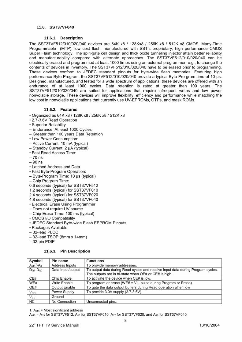
11.6.3. Pin Description Symbol Pin name Functions AMS
1-A0 Address Inputs To provide memory addresses. DQ7-DQ0 Data Input/output To output data during Read cycles and receive input data during Program cycles.
The outputs are in tri-state when OE# or CE# is high. CE# Chip Enable To activate the device when CE# is low. WE# Write Enable To program or erase (WE# = VIL pulse during Program or Erase) OE# Output Enable To gate the data output buffers during Read operation when low VDD Power Supply To provide 3.0V supply (2.7-3.6V) VSS Ground NC No Connection Unconnected pins. 1. AMS = Most significant address AMS = A15 for SST37VF512, A16 for SST37VF010, A17 for SST37VF020, and A18 for SST37VF040
9 22” TFT TV Service Manual 13/10/2004
11.7. TEA5114A
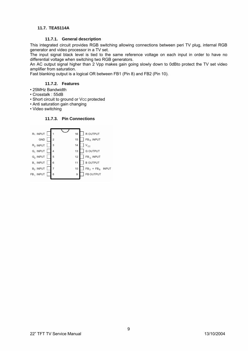
11.7.1. General description This integrated circuit provides RGB switching allowing connections between peri TV plug, internal RGB generator and video processor in a TV set. The input signal black level is tied to the same reference voltage on each input in order to have no differential voltage when switching two RGB generators. An AC output signal higher than 2 Vpp makes gain going slowly down to 0dBto protect the TV set video amplifier from saturation. Fast blanking output is a logical OR between FB1 (Pin 8) and FB2 (Pin 10).
11.7.2. Features • 25MHz Bandwidth • Crosstalk : 55dB • Short circuit to ground or VCC protected • Anti saturation gain changing • Video switching
11.7.3. Pin Connections
10 22” TFT TV Service Manual 13/10/2004
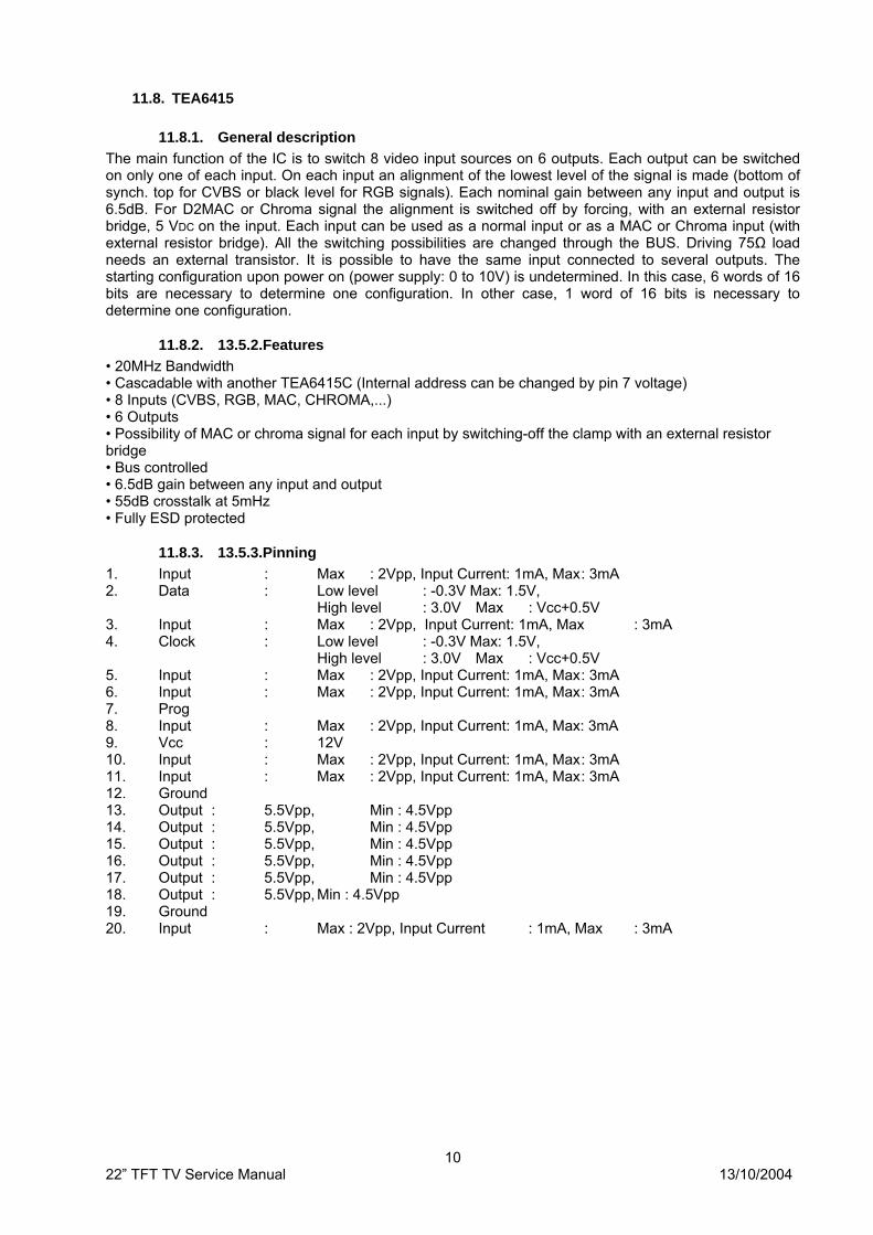
11.8. TEA6415
11.8.1. General description The main function of the IC is to switch 8 video input sources on 6 outputs. Each output can be switched on only one of each input. On each input an alignment of the lowest level of the signal is made (bottom of synch. top for CVBS or black level for RGB signals). Each nominal gain between any input and output is 6.5dB. For D2MAC or Chroma signal the alignment is switched off by forcing, with an external resistor bridge, 5 VDC on the input. Each input can be used as a normal input or as a MAC or Chroma input (with external resistor bridge). All the switching possibilities are changed through the BUS. Driving 75Ω load needs an external transistor. It is possible to have the same input connected to several outputs. The starting configuration upon power on (power supply: 0 to 10V) is undetermined. In this case, 6 words of 16 bits are necessary to determine one configuration. In other case, 1 word of 16 bits is necessary to determine one configuration.
11.8.2. 13.5.2.Features • 20MHz Bandwidth • Cascadable with another TEA6415C (Internal address can be changed by pin 7 voltage) • 8 Inputs (CVBS, RGB, MAC, CHROMA,...) • 6 Outputs • Possibility of MAC or chroma signal for each input by switching-off the clamp with an external resistor bridge • Bus controlled • 6.5dB gain between any input and output
• 55dB crosstalk at 5mHz • Fully ESD protected
11.8.3. 13.5.3.Pinning 1. Input : Max : 2Vpp, Input Current: 1mA, Max : 3mA 2. Data : Low level : -0.3V Max: 1.5V, High level : 3.0V Max : Vcc+0.5V 3. Input : Max : 2Vpp, Input Current: 1mA, Max : 3mA 4. Clock : Low level : -0.3V Max: 1.5V, High level : 3.0V Max : Vcc+0.5V 5. Input : Max : 2Vpp, Input Current: 1mA, Max : 3mA 6. Input : Max : 2Vpp, Input Current: 1mA, Max : 3mA 7. Prog 8. Input : Max : 2Vpp, Input Current: 1mA, Max: 3mA 9. Vcc : 12V 10. Input : Max : 2Vpp, Input Current: 1mA, Max : 3mA 11. Input : Max : 2Vpp, Input Current: 1mA, Max : 3mA 12. Ground 13. Output : 5.5Vpp, Min : 4.5Vpp 14. Output : 5.5Vpp, Min : 4.5Vpp 15. Output : 5.5Vpp, Min : 4.5Vpp 16. Output : 5.5Vpp, Min : 4.5Vpp 17. Output : 5.5Vpp, Min : 4.5Vpp 18. Output : 5.5Vpp, Min : 4.5Vpp 19. Ground 20. Input : Max : 2Vpp, Input Current : 1mA, Max : 3mA
11 22” TFT TV Service Manual 13/10/2004
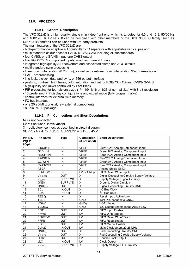
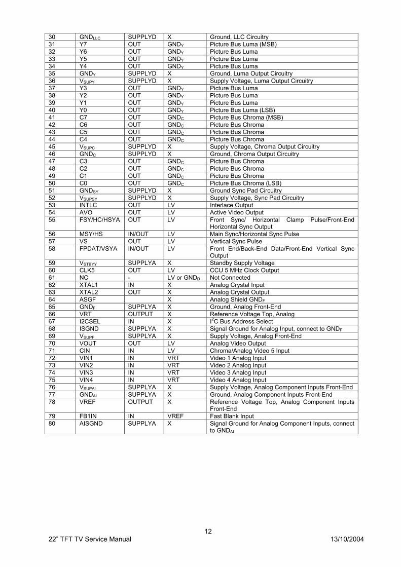
11.9. VPC3230D
11.9.1. General Description The VPC 323xD is a high-quality, single-chip video front-end, which is targeted for 4:3 and 16:9, 50/60-Hz and 100/120 Hz TV sets. It can be combined with other members of the DIGIT3000 IC family (such as DDP 331x) and/or it can be used with 3rd-party products. The main features of the VPC 323xD are • high-performance adaptive 4H comb filter Y/C separator with adjustable vertical peaking • multi-standard colour decoder PAL/NTSC/SECAM including all substandards • four CVBS, one S-VHS input, one CVBS output • two RGB/YCr Cb component inputs, one Fast Blank (FB) input • integrated high-quality A/D converters and associated clamp and AGC circuits • multi-standard sync processing • linear horizontal scaling (0.25 ... 4), as well as non-linear horizontal scaling ‘Panorama-vision’ • PAL+ preprocessing • line-locked clock, data and sync, or 656-output interface • peaking, contrast, brightness, color saturation and tint for RGB/ YC r C b and CVBS/ S-VHS • high-quality soft mixer controlled by Fast Blank • PIP processing for four picture sizes (1/4, 1/9, 1/16 or 1/36 of normal size) with 8-bit resolution • 15 predefined PIP display configurations and expert mode (fully programmable) • control interface for external field memory • I2C-bus interface • one 20.25-MHz crystal, few external components • 80-pin PQFP package
11.9.2. Pin Connections and Short Descriptions NC = not connected LV = if not used, leave vacant X = obligatory; connect as described in circuit diagram SUPPLYA = 4.75...5.25 V, SUPPLYD = 3.15...3.45 V Pin No. PQFP 80-pin
Pin Name Type Connection (if not used)
Short Description
1 B1/CB1IN IN VREF Blue1/Cb1 Analog Component Input 2 G1/Y1IN IN VREF Green1/Y1 Analog Component Input 3 R1/CR1IN IN VREF Read1/Cr1 Analog Component Input 4 B2/CB2IN IN VREF Blue2/Cb2 Analog Component Input 5 G2/Y2IN IN VREF Green2/Y2 Analog Component Input 6 R2/CR2IN IN VREF Read2/Cr2 Analog Component Input 7 ASGF X Analog Shield GNDF 8 FFRSTWIN IN LV or GNDD FIFO Reset Write Input 9 VSUPCAP OUT X Digital Decoupling Circuitry Supply Voltage 10 VSUPD SUPPLYD X Supply Voltage, Digital Circuitry 11 GNDD SUPPLYD X Ground, Digital Circuitry 12 GNDCAP OUT X Digital Decoupling Circuitry GND 13 SCL IN/OUT X I2C Bus Clock 14 SDA IN/OUT X I2C Bus Data 15 RESQ IN X Reset Input, Active Low 16 TEST IN GNDD Test Pin, connect to GNDD 17 VGAV IN GNDD VGAV Input 18 YCOEQ IN GNDD Y/C Output Enable Input, Active Low 19 FFIE OUT LV FIFO Input Enable 20 FFWE OUT LV FIFO Write Enable 21 FFRSTW OUT LV FIFO Reset Write/Read 22 FFRE OUT LV FIFO Read Enable 23 FFOE OUT LV FIFO Output Enable 24 CLK20 IN/OUT LV Main Clock output 20.25 MHz 25 GNDPA OUT X Pad Decoupling Circuitry GND 26 VSUPPA OUT X Pad Decoupling Circuitry Supply Voltage 27 LLC2 OUT LV Double Clock Output 28 LLC1 IN/OUT LV Clock Output 29 VSUPLLC SUPPLYD X Supply Voltage, LLC Circuitry
12 22” TFT TV Service Manual 13/10/2004
30 GNDLLC SUPPLYD X Ground, LLC Circuitry 31 Y7 OUT GNDY Picture Bus Luma (MSB) 32 Y6 OUT GNDY Picture Bus Luma 33 Y5 OUT GNDY Picture Bus Luma 34 Y4 OUT GNDY Picture Bus Luma 35 GNDY SUPPLYD X Ground, Luma Output Circuitry 36 VSUPY SUPPLYD X Supply Voltage, Luma Output Circuitry 37 Y3 OUT GNDY Picture Bus Luma 38 Y2 OUT GNDY Picture Bus Luma 39 Y1 OUT GNDY Picture Bus Luma 40 Y0 OUT GNDY Picture Bus Luma (LSB) 41 C7 OUT GNDC Picture Bus Chroma (MSB) 42 C6 OUT GNDC Picture Bus Chroma 43 C5 OUT GNDC Picture Bus Chroma 44 C4 OUT GNDC Picture Bus Chroma 45 VSUPC SUPPLYD X Supply Voltage, Chroma Output Circuitry 46 GNDC SUPPLYD X Ground, Chroma Output Circuitry 47 C3 OUT GNDC Picture Bus Chroma 48 C2 OUT GNDC Picture Bus Chroma 49 C1 OUT GNDC Picture Bus Chroma 50 C0 OUT GNDC Picture Bus Chroma (LSB) 51 GNDSY SUPPLYD X Ground Sync Pad Circuitry 52 VSUPSY SUPPLYD X Supply Voltage, Sync Pad Circuitry 53 INTLC OUT LV Interlace Output 54 AVO OUT LV Active Video Output 55 FSY/HC/HSYA OUT LV Front Sync/ Horizontal Clamp Pulse/Front-End
Horizontal Sync Output 56 MSY/HS IN/OUT LV Main Sync/Horizontal Sync Pulse 57 VS OUT LV Vertical Sync Pulse 58 FPDAT/VSYA IN/OUT LV Front End/Back-End Data/Front-End Vertical Sync
Output 59 VSTBYY SUPPLYA X Standby Supply Voltage 60 CLK5 OUT LV CCU 5 MHz Clock Output 61 NC - LV or GNDD Not Connected 62 XTAL1 IN X Analog Crystal Input 63 XTAL2 OUT X Analog Crystal Output 64 ASGF X Analog Shield GNDF 65 GNDF SUPPLYA X Ground, Analog Front-End 66 VRT OUTPUT X Reference Voltage Top, Analog 67 I2CSEL IN X I2C Bus Address Select 68 ISGND SUPPLYA X Signal Ground for Analog Input, connect to GNDF 69 VSUPF SUPPLYA X Supply Voltage, Analog Front-End 70 VOUT OUT LV Analog Video Output 71 CIN IN LV Chroma/Analog Video 5 Input 72 VIN1 IN VRT Video 1 Analog Input 73 VIN2 IN VRT Video 2 Analog Input 74 VIN3 IN VRT Video 3 Analog Input 75 VIN4 IN VRT Video 4 Analog Input 76 VSUPAI SUPPLYA X Supply Voltage, Analog Component Inputs Front-End 77 GNDAI SUPPLYA X Ground, Analog Component Inputs Front-End 78 VREF OUTPUT X Reference Voltage Top, Analog Component Inputs
Front-End 79 FB1IN IN VREF Fast Blank Input 80 AISGND SUPPLYA X Signal Ground for Analog Component Inputs, connect
to GNDAI
13 22” TFT TV Service Manual 13/10/2004
11.10. SDA55XX (SDA5550)
11.10.1. General description The SDA55XX is a single chip teletext decoder for decoding World System Teletext data as well as Video Programming System (VPS), Program Delivery Control (PDC), and Wide Screen Signalling (WSS) data used for PAL plus transmissions (Line 23). The device also supports Closed caption acquisition and decoding. The device provides an integrated general-purpose, fully 8051-compatible Microcontroller with television specific hardware features. Microcontroller has been enhanced to provide powerful features such as memory banking, data pointers, and additional interrupts etc. The on-chip display unit for displaying Level 1.5 teletext data can also be used for customer defined on screen displays. Internal XRAM consists of up to16 Kbytes. Device has an internal ROM of up to 128 KBytes. ROMless versions can access up to 1 MByte of external RAM and ROM. The SDA 55XX supports a wide range of standards including PAL, NTSC and contains a digital slicer for VPS, WSS, PDC, TTX and Closed Caption, an accelerating acquisition hardware module, a display generator for Level 1.5 TTX data and powerful On screen Display capabilities based on parallel attributes, and Pixel oriented characters (DRCS). The 8-bit Microcontroller runs at 360 ns. cycle time (min.). Controller with dedicated hardware does most of the internal TTX acquisition processing, transfers data to/from external memory interface and receives/ transmits data via I2C-firmware user-interface. The slicer combined with dedicated hardware stores TTX data in a VBI buffer of 1 Kilobyte. The Microcontroller firmware performs all the acquisition tasks (hamming and parity-checks, page search and evaluation of header control bits) once per field. Additionally, the firmware can provide high-end Teletext features like Packet-26-handling, FLOF, TOP and list-pages. The interface to user software is optimized for minimal overhead. SDA 55XX is realized in 0.25 micron technology with 2.5 V supply voltage and 3.3 V I/O (TTL compatible). The software and hardware development environment (TEAM) is available to simplify and speed up the development of the software and On Screen Display. TEAM stands for TVT Expert Application Maker. It improves the TV controller software quality in following aspects: – Shorter time to market – Re-usability – Target independent development – Verification and validation before targeting – General test concept – Graphical interface design requiring minimum programming and controller know how. – Modular and open tool chain, configurable by customer.
14 22” TFT TV Service Manual 13/10/2004
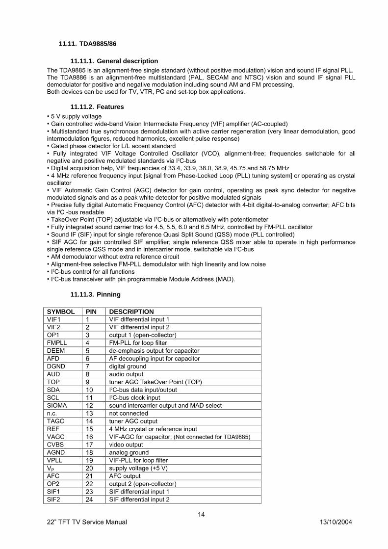
11.11. TDA9885/86
11.11.1. General description The TDA9885 is an alignment-free single standard (without positive modulation) vision and sound IF signal PLL. The TDA9886 is an alignment-free multistandard (PAL, SECAM and NTSC) vision and sound IF signal PLL demodulator for positive and negative modulation including sound AM and FM processing. Both devices can be used for TV, VTR, PC and set-top box applications.
11.11.2. Features • 5 V supply voltage • Gain controlled wide-band Vision Intermediate Frequency (VIF) amplifier (AC-coupled) • Multistandard true synchronous demodulation with active carrier regeneration (very linear demodulation, good intermodulation figures, reduced harmonics, excellent pulse response) • Gated phase detector for L/L accent standard • Fully integrated VIF Voltage Controlled Oscillator (VCO), alignment-free; frequencies switchable for all negative and positive modulated standards via I2C-bus • Digital acquisition help, VIF frequencies of 33.4, 33.9, 38.0, 38.9, 45.75 and 58.75 MHz • 4 MHz reference frequency input [signal from Phase-Locked Loop (PLL) tuning system] or operating as crystal oscillator • VIF Automatic Gain Control (AGC) detector for gain control, operating as peak sync detector for negative modulated signals and as a peak white detector for positive modulated signals • Precise fully digital Automatic Frequency Control (AFC) detector with 4-bit digital-to-analog converter; AFC bits via I2C -bus readable • TakeOver Point (TOP) adjustable via I2C-bus or alternatively with potentiometer • Fully integrated sound carrier trap for 4.5, 5.5, 6.0 and 6.5 MHz, controlled by FM-PLL oscillator • Sound IF (SIF) input for single reference Quasi Split Sound (QSS) mode (PLL controlled) • SIF AGC for gain controlled SIF amplifier; single reference QSS mixer able to operate in high performance single reference QSS mode and in intercarrier mode, switchable via I2C-bus • AM demodulator without extra reference circuit • Alignment-free selective FM-PLL demodulator with high linearity and low noise • I2C-bus control for all functions • I2C-bus transceiver with pin programmable Module Address (MAD).
11.11.3. Pinning SYMBOL PIN DESCRIPTION VIF1 1 VIF differential input 1 VIF2 2 VIF differential input 2 OP1 3 output 1 (open-collector) FMPLL 4 FM-PLL for loop filter DEEM 5 de-emphasis output for capacitor AFD 6 AF decoupling input for capacitor DGND 7 digital ground AUD 8 audio output TOP 9 tuner AGC TakeOver Point (TOP) SDA 10 I2C-bus data input/output SCL 11 I2C-bus clock input SIOMA 12 sound intercarrier output and MAD select n.c. 13 not connected TAGC 14 tuner AGC output REF 15 4 MHz crystal or reference input VAGC 16 VIF-AGC for capacitor; (Not connected for TDA9885) CVBS 17 video output AGND 18 analog ground VPLL 19 VIF-PLL for loop filter VP 20 supply voltage (+5 V) AFC 21 AFC output OP2 22 output 2 (open-collector) SIF1 23 SIF differential input 1 SIF2 24 SIF differential input 2
15 22” TFT TV Service Manual 13/10/2004
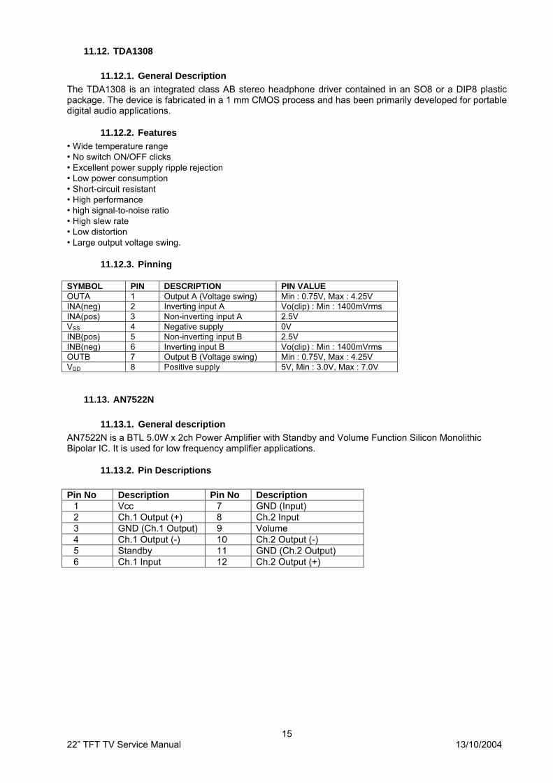
11.12. TDA1308
11.12.1. General Description The TDA1308 is an integrated class AB stereo headphone driver contained in an SO8 or a DIP8 plastic package. The device is fabricated in a 1 mm CMOS process and has been primarily developed for portable digital audio applications.
11.12.2. Features • Wide temperature range • No switch ON/OFF clicks • Excellent power supply ripple rejection • Low power consumption • Short-circuit resistant • High performance • high signal-to-noise ratio • High slew rate • Low distortion • Large output voltage swing.
11.12.3. Pinning SYMBOL PIN DESCRIPTION PIN VALUE OUTA 1 Output A (Voltage swing) Min : 0.75V, Max : 4.25V INA(neg) 2 Inverting input A Vo(clip) : Min : 1400mVrms INA(pos) 3 Non-inverting input A 2.5V VSS 4 Negative supply 0V INB(pos) 5 Non-inverting input B 2.5V INB(neg) 6 Inverting input B Vo(clip) : Min : 1400mVrms OUTB 7 Output B (Voltage swing) Min : 0.75V, Max : 4.25V VDD 8 Positive supply 5V, Min : 3.0V, Max : 7.0V
11.13. AN7522N
11.13.1. General description AN7522N is a BTL 5.0W x 2ch Power Amplifier with Standby and Volume Function Silicon Monolithic Bipolar IC. It is used for low frequency amplifier applications.
11.13.2. Pin Descriptions Pin No Description Pin No Description
1 Vcc 7 GND (Input) 2 Ch.1 Output (+) 8 Ch.2 Input 3 GND (Ch.1 Output) 9 Volume 4 Ch.1 Output (-) 10 Ch.2 Output (-) 5 Standby 11 GND (Ch.2 Output) 6 Ch.1 Input 12 Ch.2 Output (+)
16 22” TFT TV Service Manual 13/10/2004
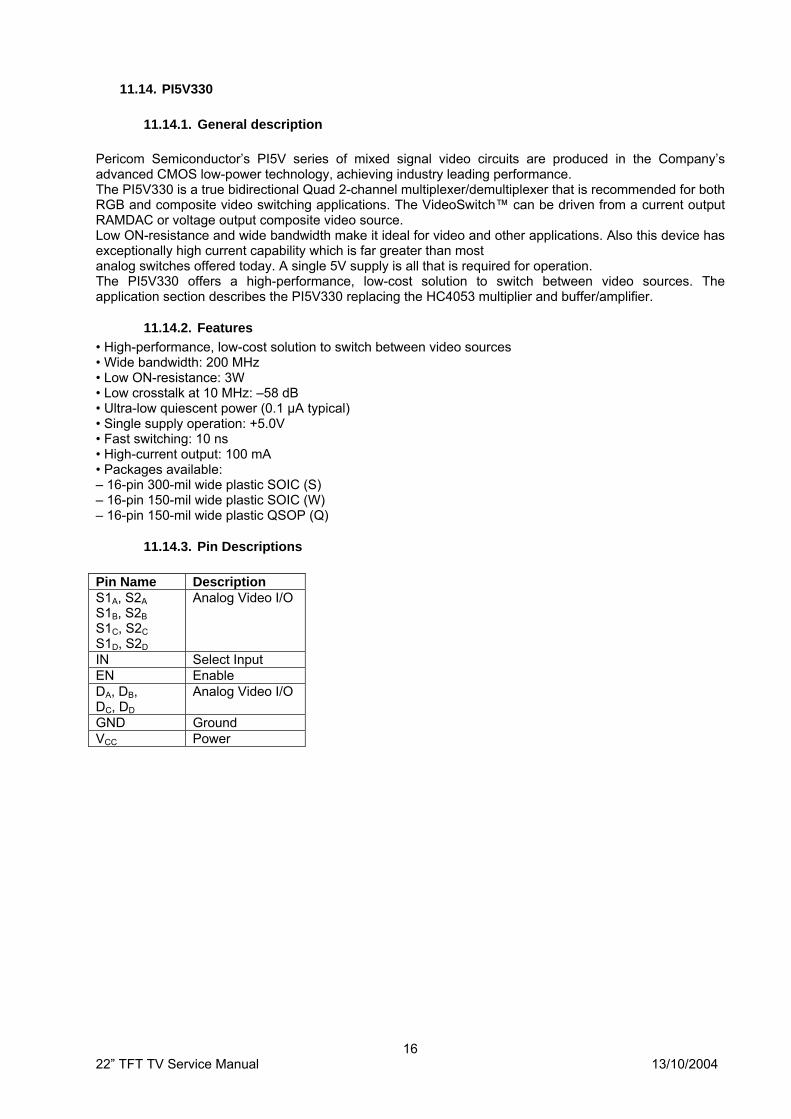
11.14. PI5V330
11.14.1. General description Pericom Semiconductor’s PI5V series of mixed signal video circuits are produced in the Company’s advanced CMOS low-power technology, achieving industry leading performance. The PI5V330 is a true bidirectional Quad 2-channel multiplexer/demultiplexer that is recommended for both RGB and composite video switching applications. The VideoSwitch™ can be driven from a current output RAMDAC or voltage output composite video source. Low ON-resistance and wide bandwidth make it ideal for video and other applications. Also this device has exceptionally high current capability which is far greater than most analog switches offered today. A single 5V supply is all that is required for operation. The PI5V330 offers a high-performance, low-cost solution to switch between video sources. The application section describes the PI5V330 replacing the HC4053 multiplier and buffer/amplifier.
11.14.2. Features • High-performance, low-cost solution to switch between video sources • Wide bandwidth: 200 MHz • Low ON-resistance: 3W • Low crosstalk at 10 MHz: –58 dB • Ultra-low quiescent power (0.1 µA typical) • Single supply operation: +5.0V • Fast switching: 10 ns • High-current output: 100 mA • Packages available: – 16-pin 300-mil wide plastic SOIC (S) – 16-pin 150-mil wide plastic SOIC (W) – 16-pin 150-mil wide plastic QSOP (Q)
11.14.3. Pin Descriptions Pin Name Description S1A, S2A S1B, S2B S1C, S2C S1D, S2D
Analog Video I/O
IN Select Input EN Enable DA, DB, DC, DD
Analog Video I/O
GND Ground VCC Power
17 22” TFT TV Service Manual 13/10/2004
11.15. GM6015
11.15.1. General description The Genesis Microchip 6015RD1 LCD TV reference board is a complete display processor for LCD, PDP and LCOS based televisions. The reference board demonstrates the processing capabilities of the Genesis Microchip gm6015 television controller IC. The gm6015 IC is a full-featured, dual-channel video processor with Genesis industry leading Crystal Ciema PlusTM video scan conversion. The 6015RD1 board inputs analog YPbPr/RGB, NTSC/PAL/SECAM CVBS/YC, UHF/VHF and outputs digital RGB to an XGA LCD panel. A convenient on-screen display system provides easy control of the board’s processing capabilities. The design kit is complete with hardware and software. Software includes G-Probe debug software, G-Wizard register calculator and G-TV application source code. The 6015RD1 is a related reference board that outputs analog YpbPr/RGB.
11.15.2. Features • Dual channel, gm6015 based LCD TV system • Industry leading Crystal Cinema Plus video scan conversion • Inputs:
i. Component analog YPbPr/RGB ii. 480/576I, 480/576P, 720P and 1080I HD iii. Dual NTSC/PAL/SECAM CVBS and YC iv. VGA, SVGA, XGA PC graphics v. Separate, composite or sync on Y/G vi. UHF/VHF RF (NTSC)
• Default output with XGA LCD interface PCB: i. Component analog YpbPr/RGB
• Other outputs: ii. 8/16/20/24-bit 4:2:2/4:4:4 digital YCbCr/RGB iii. 480/576I, 480/576P, 720P and 1080I HD iv. VGA, SVGA, XGA PC graphics v. Separate, composite or sync on Y/G
• On-screen display (OSD) user interface with automated self running demonstration • Small form factor PCB
18 22” TFT TV Service Manual 13/10/2004
11.16. SAA3010T
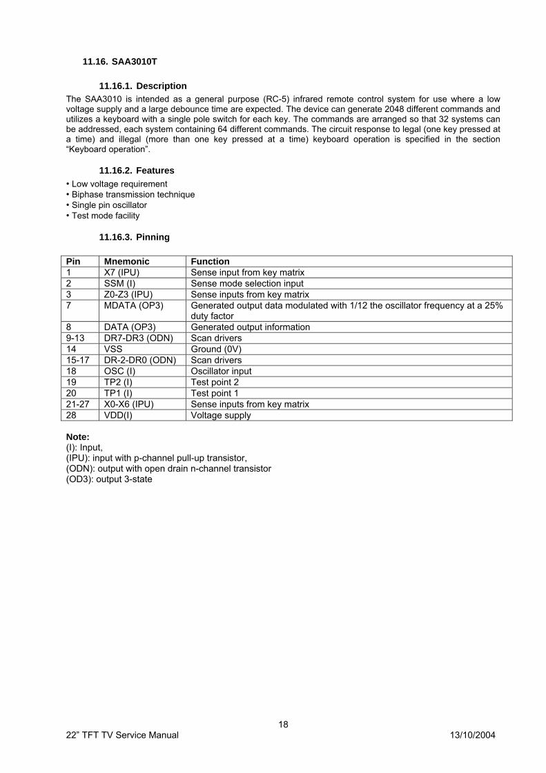
11.16.1. Description The SAA3010 is intended as a general purpose (RC-5) infrared remote control system for use where a low voltage supply and a large debounce time are expected. The device can generate 2048 different commands and utilizes a keyboard with a single pole switch for each key. The commands are arranged so that 32 systems can be addressed, each system containing 64 different commands. The circuit response to legal (one key pressed at a time) and illegal (more than one key pressed at a time) keyboard operation is specified in the section “Keyboard operation”.
11.16.2. Features • Low voltage requirement • Biphase transmission technique • Single pin oscillator • Test mode facility
11.16.3. Pinning Pin Mnemonic Function 1 X7 (IPU) Sense input from key matrix 2 SSM (I) Sense mode selection input 3 Z0-Z3 (IPU) Sense inputs from key matrix 7 MDATA (OP3) Generated output data modulated with 1/12 the oscillator frequency at a 25%
duty factor 8 DATA (OP3) Generated output information 9-13 DR7-DR3 (ODN) Scan drivers 14 VSS Ground (0V) 15-17 DR-2-DR0 (ODN) Scan drivers 18 OSC (I) Oscillator input 19 TP2 (I) Test point 2 20 TP1 (I) Test point 1 21-27 X0-X6 (IPU) Sense inputs from key matrix 28 VDD(I) Voltage supply Note: (I): Input, (IPU): input with p-channel pull-up transistor, (ODN): output with open drain n-channel transistor (OD3): output 3-state
19 22” TFT TV Service Manual 13/10/2004
11.17. AD9883A
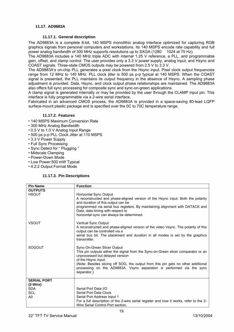
11.17.1. General description The AD9883A is a complete 8-bit, 140 MSPS monolithic analog interface optimized for capturing RGB graphics signals from personal computers and workstations. Its 140 MSPS encode rate capability and full power analog bandwidth of 300 MHz supports resolutions up to SXGA (1280 1024 at 75 Hz). The AD9883A includes a 140 MHz triple ADC with internal 1.25 V reference, a PLL, and programmable gain, offset, and clamp control. The user provides only a 3.3 V power supply, analog input, and Hsync and COAST signals. Three-state CMOS outputs may be powered from 2.5 V to 3.3 V. The AD9883A’s on-chip PLL generates a pixel clock from the Hsync input. Pixel clock output frequencies range from 12 MHz to 140 MHz. PLL clock jitter is 500 ps p-p typical at 140 MSPS. When the COAST signal is presented, the PLL maintains its output frequency in the absence of Hsync. A sampling phase adjustment is provided. Data, Hsync, and clock output phase relationships are maintained. The AD9883A also offers full sync processing for composite sync and sync-on-green applications. A clamp signal is generated internally or may be provided by the user through the CLAMP input pin. This interface is fully programmable via a 2-wire serial interface. Fabricated in an advanced CMOS process, the AD9883A is provided in a space-saving 80-lead LQFP surface-mount plastic package and is specified over the 0C to 70C temperature range.
11.17.2. Features • 140 MSPS Maximum Conversion Rate • 300 MHz Analog Bandwidth • 0.5 V to 1.0 V Analog Input Range • 500 ps p-p PLL Clock Jitter at 110 MSPS • 3.3 V Power Supply • Full Sync Processing • Sync Detect for “ Plugging ” • Midscale Clamping • Power-Down Mode • Low Power:500 mW Typical • 4:2:2 Output Format Mode
11.17.3. Pin Descriptions Pin Name Function OUTPUTS HSOUT VSOUT SOGOUT
Horizontal Sync Output A reconstructed and phase-aligned version of the Hsync input. Both the polarity and duration of this output can be programmed via serial bus registers. By maintaining alignment with DATACK and Data, data timing with respect to horizontal sync can always be determined. Vertical Sync Output A reconstructed and phase-aligned version of the video Vsync. The polarity of this output can be controlled via a serial bus bit. The placement and duration in all modes is set by the graphics transmitter. Sync-On-Green Slicer Output This pin outputs either the signal from the Sync-on-Green slicer comparator or an unprocessed but delayed version of the Hsync input. (Note: Besides slicing off SOG, the output from this pin gets no other additional processing on the AD9883A. Vsync separation is performed via the sync separator.)
SERIAL PORT (2-Wire) SDA SCL A0
Serial Port Data I/O Serial Port Data Clock Serial Port Address Input 1 For a full description of the 2-wire serial register and how it works, refer to the 2-Wire Serial Control Port section.
20 22” TFT TV Service Manual 13/10/2004
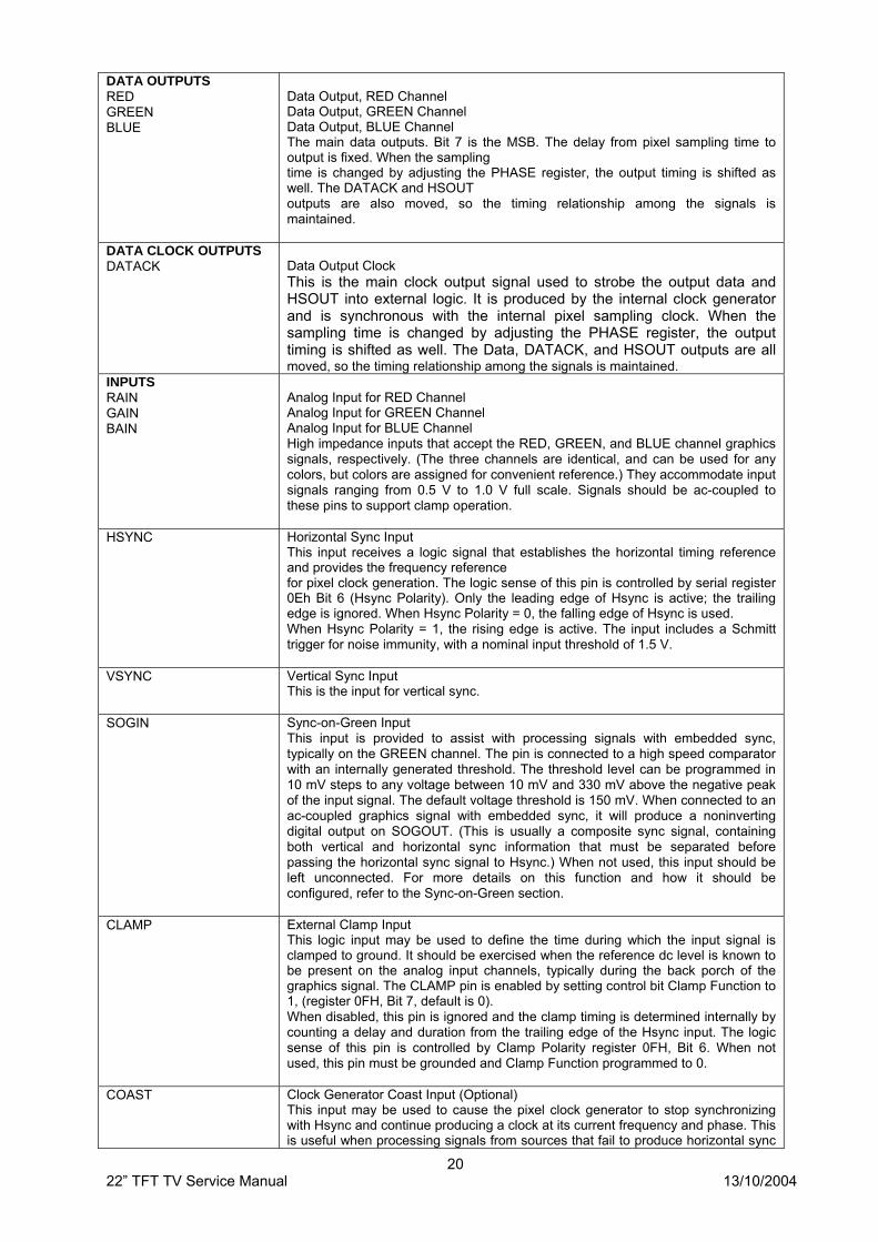
DATA OUTPUTS RED GREEN BLUE
Data Output, RED Channel Data Output, GREEN Channel Data Output, BLUE Channel The main data outputs. Bit 7 is the MSB. The delay from pixel sampling time to output is fixed. When the sampling time is changed by adjusting the PHASE register, the output timing is shifted as well. The DATACK and HSOUT outputs are also moved, so the timing relationship among the signals is maintained.
DATA CLOCK OUTPUTS DATACK
Data Output Clock This is the main clock output signal used to strobe the output data and HSOUT into external logic. It is produced by the internal clock generator and is synchronous with the internal pixel sampling clock. When the sampling time is changed by adjusting the PHASE register, the output timing is shifted as well. The Data, DATACK, and HSOUT outputs are all moved, so the timing relationship among the signals is maintained.
INPUTS RAIN GAIN BAIN
Analog Input for RED Channel Analog Input for GREEN Channel Analog Input for BLUE Channel High impedance inputs that accept the RED, GREEN, and BLUE channel graphics signals, respectively. (The three channels are identical, and can be used for any colors, but colors are assigned for convenient reference.) They accommodate input signals ranging from 0.5 V to 1.0 V full scale. Signals should be ac-coupled to these pins to support clamp operation.
HSYNC Horizontal Sync Input This input receives a logic signal that establishes the horizontal timing reference and provides the frequency reference for pixel clock generation. The logic sense of this pin is controlled by serial register 0Eh Bit 6 (Hsync Polarity). Only the leading edge of Hsync is active; the trailing edge is ignored. When Hsync Polarity = 0, the falling edge of Hsync is used. When Hsync Polarity = 1, the rising edge is active. The input includes a Schmitt trigger for noise immunity, with a nominal input threshold of 1.5 V.
VSYNC Vertical Sync Input This is the input for vertical sync.
SOGIN Sync-on-Green Input This input is provided to assist with processing signals with embedded sync, typically on the GREEN channel. The pin is connected to a high speed comparator with an internally generated threshold. The threshold level can be programmed in 10 mV steps to any voltage between 10 mV and 330 mV above the negative peak of the input signal. The default voltage threshold is 150 mV. When connected to an ac-coupled graphics signal with embedded sync, it will produce a noninverting digital output on SOGOUT. (This is usually a composite sync signal, containing both vertical and horizontal sync information that must be separated before passing the horizontal sync signal to Hsync.) When not used, this input should be left unconnected. For more details on this function and how it should be configured, refer to the Sync-on-Green section.
CLAMP External Clamp Input This logic input may be used to define the time during which the input signal is clamped to ground. It should be exercised when the reference dc level is known to be present on the analog input channels, typically during the back porch of the graphics signal. The CLAMP pin is enabled by setting control bit Clamp Function to 1, (register 0FH, Bit 7, default is 0). When disabled, this pin is ignored and the clamp timing is determined internally by counting a delay and duration from the trailing edge of the Hsync input. The logic sense of this pin is controlled by Clamp Polarity register 0FH, Bit 6. When not used, this pin must be grounded and Clamp Function programmed to 0.
COAST Clock Generator Coast Input (Optional) This input may be used to cause the pixel clock generator to stop synchronizing with Hsync and continue producing a clock at its current frequency and phase. This is useful when processing signals from sources that fail to produce horizontal sync
21 22” TFT TV Service Manual 13/10/2004
pulses during the vertical interval. The COAST signal is generally not required for PC-generated signals. The logic sense of this pin is controlled by Coast Polarity (register 0FH, Bit 3). When not used, this pin may be grounded and Coast Polarity programmed to 1, or tied HIGH (to VD through a 10 k resistor) and Coast Polarity programmed to 0. Coast Polarity defaults to 1 at power-up.
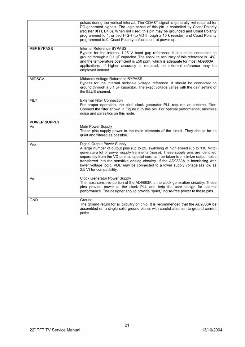
REF BYPASS Internal Reference BYPASS Bypass for the internal 1.25 V band gap reference. It should be connected to ground through a 0.1 µF capacitor. The absolute accuracy of this reference is ±4%, and the temperature coefficient is ±50 ppm, which is adequate for most AD9883A applications. If higher accuracy is required, an external reference may be employed instead.
MIDSCV Midscale Voltage Reference BYPASS Bypass for the internal midscale voltage reference. It should be connected to ground through a 0.1 µF capacitor. The exact voltage varies with the gain setting of the BLUE channel.
FILT External Filter Connection For proper operation, the pixel clock generator PLL requires an external filter. Connect the filter shown in Figure 6 to this pin. For optimal performance, minimize noise and parasitics on this node.
POWER SUPPLY VD
Main Power Supply These pins supply power to the main elements of the circuit. They should be as quiet and filtered as possible.
VDD
Digital Output Power Supply A large number of output pins (up to 25) switching at high speed (up to 110 MHz) generate a lot of power supply transients (noise). These supply pins are identified separately from the VD pins so special care can be taken to minimize output noise transferred into the sensitive analog circuitry. If the AD9883A is interfacing with lower voltage logic, VDD may be connected to a lower supply voltage (as low as 2.5 V) for compatibility.
VD
Clock Generator Power Supply The most sensitive portion of the AD9883A is the clock generation circuitry. These pins provide power to the clock PLL and help the user design for optimal performance. The designer should provide “quiet,” noise-free power to these pins.
GND Ground The ground return for all circuitry on chip. It is recommended that the AD9883A be assembled on a single solid ground plane, with careful attention to ground current paths.
22 22” TFT TV Service Manual 13/10/2004
11.18. MC141585
11.18.1. General description This is a high performance HCMOS device designed to interface with a micro controller unit to allow colored symbols or characters to be displayed onto a LCD monitor. Because of the large number of fonts, 512 fonts including 496 standard fonts and 16 multi-color fonts, LMOSD2-16 is suitable to be adopted for the multi-language monitor application especially. It minimizes the MCU’s burden through its built-in RAM. By storing a full screen of data and control information, this device has a capability to carry out ‘screen-refresh’ without any MCU supervision. Programmable hatch pattern generator is added for individual pixel inspection. Since there is no clearance between characters, special graphics oriented characters can be generated by combining two or more character blocks. The full OSD menu is formed of 15 rows x 30 columns which can by freely positioned on anywhere of the monitor screen by changing vertical or horizontal delay. Special functions such as character background color, blinking, bordering or shadowing, four-level windows with programmable size, row double height and double width, programmable vertical height of character and row-to-row spacing, and full-screen erasing and Fade-In/Fade-Out are also incorporated. There are 8 color selections for any individual character display with row intensity attribute and window intensity attribute to expand the color mixture on OSD menu.
11.18.2. Features • Totally 512 Fonts Including 496 Standard Fonts and 16 Multi-Color Fonts. • 10x18 or 12x18 Font Matrix Selection • Maximum Pixel CLK of 80MHz • Maximum input resolution of 1580 dots/line (PIXin/HSYNC ratio) • Wide Operating Frequency: max. 150KHz for Monitor • Fully Programmable Character Array of 15 Rows by 30 Columns • 8-Color Selection for Characters with Color Intensity Attribute on Each Row • 7-Color Selection for Characters background • True 16-Color Selection for Windows • Shadowing on Windows with Programmable Shadow Width/Height/Color • Fancy Fade-In/Fade-Out Effects • Programmable Height of Character to Meet Multi-Sync Requirement • Row To Row Spacing Control to Avoid Expansion Distortion • Four Programmable Windows with Overlapping Capability • Character Bordering or Shadowing • Character/Symbol Blinking Function • Programmable Vertical and Horizontal Positioning for Display Center • M_BUS (IIC) Interface with Address $7A
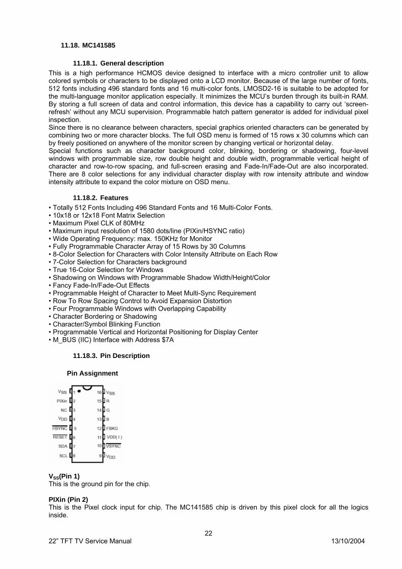
11.18.3. Pin Description
Pin Assignment
VSS(Pin 1) This is the ground pin for the chip. PIXin (Pin 2) This is the Pixel clock input for chip. The MC141585 chip is driven by this pixel clock for all the logics inside.
23 22” TFT TV Service Manual 13/10/2004
NC (Pin 3) No connection. VDD (Pin 4) This is the +5V power pin for the chip. HSYNC (Pin 5) This pin inputs a horizontal synchronize signal. It is negative polarity by default. The leading edge of HSYNC synchronizes its internal horizontal timing. The maximum input ratio between PIXin/HSYNC should not greater than 1580 for displaying 12X18 font matrix. For displaying 10X18 font matrix, this ratio should not greater than 1280. RESET (Pin 6) An active low signal will reset ROW15 and ROW16 control registers. Refer to Control Registers section for default set-tings. A proper RC network have to be tighten to this pin to ensure the device initialize properly during power up. Refer to the application diagram. SDA (Pin 7) Data and control message are being transmitted to this chip from a host MCU via M_bus systems. This wire is configurated as a uni-directional data line. (Detailed description of protocols will be discussed in the M_BUS section). SCL (Pin 8) A separate synchronizing clock input from the transmitter is required for M_Bus protocol. Data is read at the rising edge of each clock signal. VDD (Pin 9) This is the power pin for the digital logic of the chip. VSYNC (Pin 10) Similar to Pin 5, this pin inputs a vertical synchronize signal to synchronize the vertical control circuit. It is negative polarity by default. VDD (I) (Pin 11) This is the voltage supply of RGB outputs when low intensity of Windows/ROW is selected. The RBG output level would be equal to VDD(I) in this case. Please refer to Row Attribute/Window registers for more detail. The input voltage for this pin should be equal to or less than V DD (Pin 17) for normal operation. FBKG (Pin 12) This pin will output a logic high while displaying characters or windows. It is defaulted to high impedance state after power on, or when there is no output. An external 10 κΩ resistor pulled low is recommended to avoid level toggling caused by hand effect when there is no output. B,G,R (Pin 13, 14, 15) LMOSD2-16 color outputs in CMOS level to the host monitor. These three signals are open drain outputs if 3_STATE bit is set and the color intensity is inactive. Otherwise, they are active high push-pull outputs. See “REGISTERS” for more information. These pins are in high impedance state after power on. VSS (Pin 24) This is the ground pin for the digital logic of the chip.
24 22” TFT TV Service Manual 13/10/2004
11.19. MC34063
11.19.1. Description The MC34063A Series is a monolithic control circuit containing the primary functions required for DC–to–DC converters. These devices consist of an internal temperature compensated reference, comparator, controlled duty cycle oscillator with an active current limit circuit, driver and high current output switch. This series was specifically designed to be incorporated in Step–Down and Step–Up and Voltage–Inverting applications with a minimum number of external components.
11.19.2. Features • Operation from 3.0 V to 40 V Input • Low Standby Current • Current Limiting • Output Switch Current to 1.5 A • Output Voltage Adjustable • Frequency Operation to 100 kHz • Precision 2% Reference
11.19.3. Pin connections
25 22” TFT TV Service Manual 13/10/2004
11.20. MSP34X0G MSP3400G Multistandard Sound Processor Family
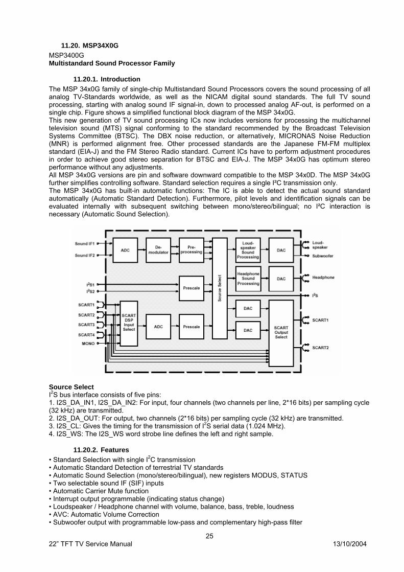
11.20.1. Introduction The MSP 34x0G family of single-chip Multistandard Sound Processors covers the sound processing of all analog TV-Standards worldwide, as well as the NICAM digital sound standards. The full TV sound processing, starting with analog sound IF signal-in, down to processed analog AF-out, is performed on a single chip. Figure shows a simplified functional block diagram of the MSP 34x0G. This new generation of TV sound processing ICs now includes versions for processing the multichannel television sound (MTS) signal conforming to the standard recommended by the Broadcast Television Systems Committee (BTSC). The DBX noise reduction, or alternatively, MICRONAS Noise Reduction (MNR) is performed alignment free. Other processed standards are the Japanese FM-FM multiplex standard (EIA-J) and the FM Stereo Radio standard. Current ICs have to perform adjustment procedures in order to achieve good stereo separation for BTSC and EIA-J. The MSP 34x0G has optimum stereo performance without any adjustments. All MSP 34x0G versions are pin and software downward compatible to the MSP 34x0D. The MSP 34x0G further simplifies controlling software. Standard selection requires a single I²C transmission only. The MSP 34x0G has built-in automatic functions: The IC is able to detect the actual sound standard automatically (Automatic Standard Detection). Furthermore, pilot levels and identification signals can be evaluated internally with subsequent switching between mono/stereo/bilingual; no I²C interaction is necessary (Automatic Sound Selection).
Source Select I2S bus interface consists of five pins: 1. I2S_DA_IN1, I2S_DA_IN2: For input, four channels (two channels per line, 2*16 bits) per sampling cycle (32 kHz) are transmitted. 2. I2S_DA_OUT: For output, two channels (2*16 bits) per sampling cycle (32 kHz) are transmitted. 3. I2S_CL: Gives the timing for the transmission of I2S serial data (1.024 MHz). 4. I2S_WS: The I2S_WS word strobe line defines the left and right sample.
11.20.2. Features • Standard Selection with single I2C transmission • Automatic Standard Detection of terrestrial TV standards • Automatic Sound Selection (mono/stereo/bilingual), new registers MODUS, STATUS • Two selectable sound IF (SIF) inputs • Automatic Carrier Mute function • Interrupt output programmable (indicating status change) • Loudspeaker / Headphone channel with volume, balance, bass, treble, loudness • AVC: Automatic Volume Correction • Subwoofer output with programmable low-pass and complementary high-pass filter
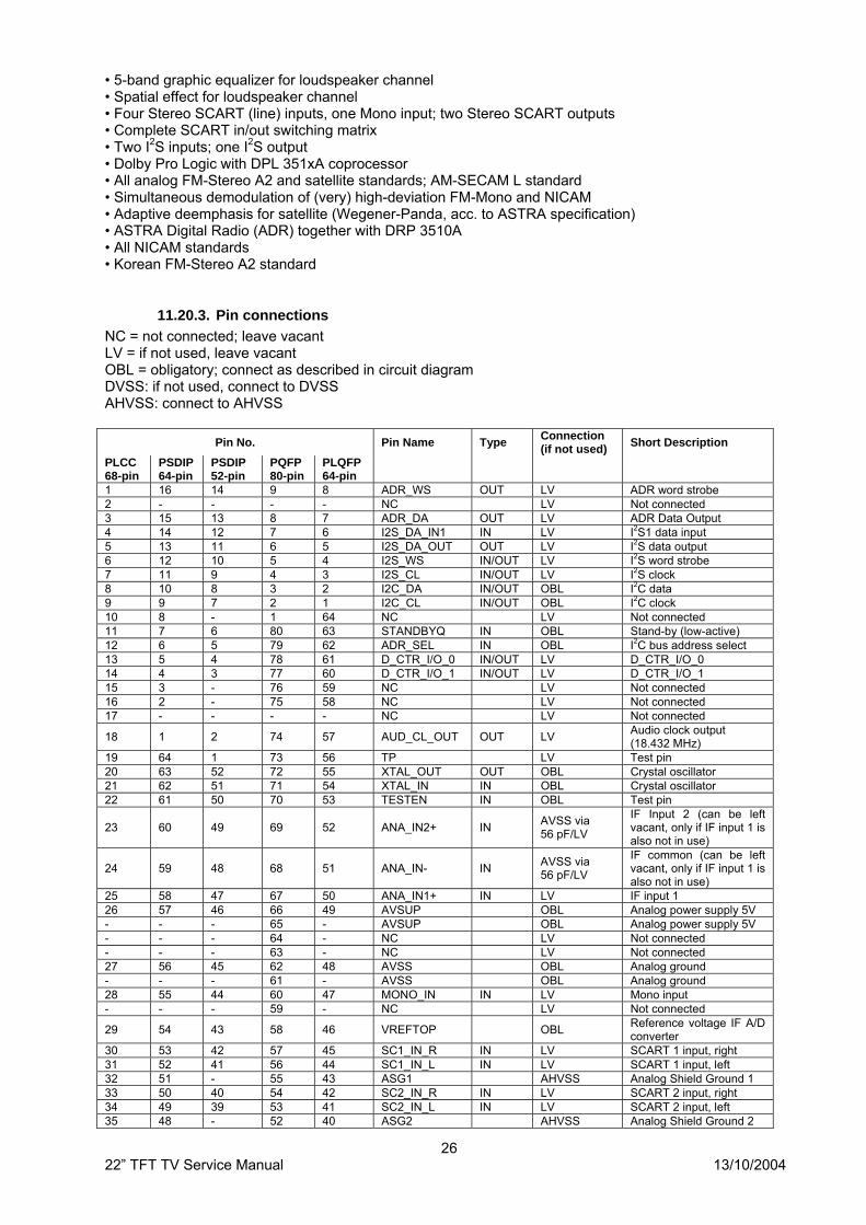
26 22” TFT TV Service Manual 13/10/2004
• 5-band graphic equalizer for loudspeaker channel • Spatial effect for loudspeaker channel • Four Stereo SCART (line) inputs, one Mono input; two Stereo SCART outputs • Complete SCART in/out switching matrix • Two I2S inputs; one I2S output • Dolby Pro Logic with DPL 351xA coprocessor • All analog FM-Stereo A2 and satellite standards; AM-SECAM L standard • Simultaneous demodulation of (very) high-deviation FM-Mono and NICAM • Adaptive deemphasis for satellite (Wegener-Panda, acc. to ASTRA specification) • ASTRA Digital Radio (ADR) together with DRP 3510A • All NICAM standards • Korean FM-Stereo A2 standard
11.20.3. Pin connections NC = not connected; leave vacant LV = if not used, leave vacant OBL = obligatory; connect as described in circuit diagram DVSS: if not used, connect to DVSS AHVSS: connect to AHVSS
Pin No. Pin Name Type Connection (if not used) Short Description
PLCC 68-pin
PSDIP 64-pin
PSDIP 52-pin
PQFP 80-pin
PLQFP 64-pin
1 16 14 9 8 ADR_WS OUT LV ADR word strobe 2 - - - - NC LV Not connected 3 15 13 8 7 ADR_DA OUT LV ADR Data Output 4 14 12 7 6 I2S_DA_IN1 IN LV I2S1 data input 5 13 11 6 5 I2S_DA_OUT OUT LV I2S data output 6 12 10 5 4 I2S_WS IN/OUT LV I2S word strobe 7 11 9 4 3 I2S_CL IN/OUT LV I2S clock 8 10 8 3 2 I2C_DA IN/OUT OBL I2C data 9 9 7 2 1 I2C_CL IN/OUT OBL I2C clock 10 8 - 1 64 NC LV Not connected 11 7 6 80 63 STANDBYQ IN OBL Stand-by (low-active) 12 6 5 79 62 ADR_SEL IN OBL I2C bus address select 13 5 4 78 61 D_CTR_I/O_0 IN/OUT LV D_CTR_I/O_0 14 4 3 77 60 D_CTR_I/O_1 IN/OUT LV D_CTR_I/O_1 15 3 - 76 59 NC LV Not connected 16 2 - 75 58 NC LV Not connected 17 - - - - NC LV Not connected
18 1 2 74 57 AUD_CL_OUT OUT LV Audio clock output (18.432 MHz)
19 64 1 73 56 TP LV Test pin 20 63 52 72 55 XTAL_OUT OUT OBL Crystal oscillator 21 62 51 71 54 XTAL_IN IN OBL Crystal oscillator 22 61 50 70 53 TESTEN IN OBL Test pin
23 60 49 69 52 ANA_IN2+ IN AVSS via 56 pF/LV
IF Input 2 (can be left vacant, only if IF input 1 is also not in use)
24 59 48 68 51 ANA_IN- IN AVSS via 56 pF/LV
IF common (can be left vacant, only if IF input 1 is also not in use)
25 58 47 67 50 ANA_IN1+ IN LV IF input 1 26 57 46 66 49 AVSUP OBL Analog power supply 5V - - - 65 - AVSUP OBL Analog power supply 5V - - - 64 - NC LV Not connected - - - 63 - NC LV Not connected 27 56 45 62 48 AVSS OBL Analog ground - - - 61 - AVSS OBL Analog ground 28 55 44 60 47 MONO_IN IN LV Mono input - - - 59 - NC LV Not connected
29 54 43 58 46 VREFTOP OBL Reference voltage IF A/D converter
30 53 42 57 45 SC1_IN_R IN LV SCART 1 input, right 31 52 41 56 44 SC1_IN_L IN LV SCART 1 input, left 32 51 - 55 43 ASG1 AHVSS Analog Shield Ground 1 33 50 40 54 42 SC2_IN_R IN LV SCART 2 input, right 34 49 39 53 41 SC2_IN_L IN LV SCART 2 input, left 35 48 - 52 40 ASG2 AHVSS Analog Shield Ground 2
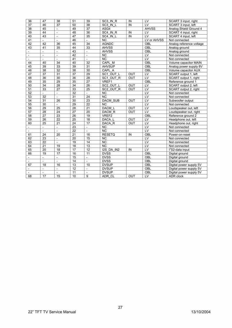
27 22” TFT TV Service Manual 13/10/2004
36 47 38 51 39 SC3_IN_R IN LV SCART 3 input, right 37 46 37 50 38 SC3_IN_L IN LV SCART 3 input, left 38 45 - 49 37 ASG4 AHVSS Analog Shield Ground 4 39 44 - 48 36 SC4_IN_R IN LV SCART 4 input, right 40 43 - 47 35 SC4_IN_L IN LV SCART 4 input, left 41 - - 46 - NC LV or AHVSS Not connected 42 42 36 45 34 AGNDC OBL Analog reference voltage 43 41 35 44 33 AHVSS OBL Analog ground - - - 43 - AHVSS OBL Analog ground - - - 42 - NC LV Not connected - - - 41 - NC LV Not connected 44 40 34 40 32 CAPL_M OBL Volume capacitor MAIN 45 39 33 39 31 AHVSUP OBL Analog power supply 8V 46 38 32 38 30 CAPL_A OBL Volume capacitor AUX 47 37 31 37 29 SC1_OUT_L OUT LV SCART output 1, left 48 36 30 36 28 SC1_OUT_R OUT LV SCART output 1, right 49 35 29 35 27 VREF1 OBL Reference ground 1 50 34 28 34 26 SC2_OUT_L OUT LV SCART output 2, left 51 33 27 33 25 SC2_OUT_R OUT LV SCART output 2, right 52 - - 32 - NC LV Not connected 53 32 - 31 24 NC LV Not connected 54 31 26 30 23 DACM_SUB OUT LV Subwoofer output 55 30 - 29 22 NC LV Not connected 56 29 25 28 21 DACM_L OUT LV Loudspeaker out, left 57 28 24 27 20 DACM_R OUT LV Loudspeaker out, right 58 27 23 26 19 VREF2 OBL Reference ground 2 59 26 22 25 18 DACA_L OUT LV Headphone out, left 60 25 21 24 17 DACA_R OUT LV Headphone out, right - - - 23 - NC LV Not connected - - - 22 - NC LV Not connected 61 24 20 21 16 RESETQ IN OBL Power-on-reset 62 23 - 20 15 NC LV Not connected 63 22 - 19 14 NC LV Not connected 64 21 19 18 13 NC LV Not connected 65 20 18 17 12 I2S_DA_IN2 IN LV I2S2-data input 66 19 17 16 11 DVSS OBL Digital ground - - - 15 - DVSS OBL Digital ground - - - 14 - DVSS OBL Digital ground 67 18 16 13 10 DVSUP OBL Digital power supply 5V - - - 12 - DVSUP OBL Digital power supply 5V - - - 11 - DVSUP OBL Digital power supply 5V 68 17 15 10 9 ADR_CL OUT LV ADR clock
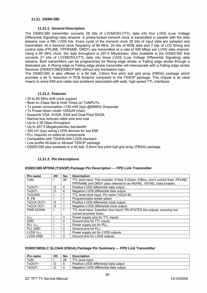
28 22” TFT TV Service Manual 13/10/2004
11.21. DS90C385
11.21.1. General Description The DS90C385 transmitter converts 28 bits of LVCMOS/LVTTL data into four LVDS (Low Voltage Differential Signaling) data streams. A phase-locked transmit clock is transmitted in parallel with the data streams over a fifth LVDS link. Every cycle of the transmit clock 28 bits of input data are sampled and transmitted. At a transmit clock frequency of 85 MHz, 24 bits of RGB data and 3 bits of LCD timing and control data (FPLINE, FPFRAME, DRDY) are transmitted at a rate of 595 Mbps per LVDS data channel. Using a 85 MHz clock, the data throughput is 297.5 Mbytes/sec. Also available is the DS90C365 that converts 21 bits of LVCMOS/LVTTL data into three LVDS (Low Voltage Differential Signaling) data streams. Both transmitters can be programmed for Rising edge strobe or Falling edge strobe through a dedicated pin. A Rising edge or Falling edge strobe transmitter will interoperate with a Falling edge strobe Receiver (DS90CF386/DS90CF366) without any translation logic. The DS90C385 is also offered in a 64 ball, 0.8mm fine pitch ball grid array (FBGA) package which provides a 44 % reduction in PCB footprint compared to the TSSOP package. This chipset is an ideal means to solve EMI and cable size problems associated with wide, high-speed TTL interfaces.
11.21.2. Features • 20 to 85 MHz shift clock support • Best–in–Class Set & Hold Times on TxINPUTs • Tx power consumption <130 mW (typ) @85MHz Grayscale • Tx Power-down mode <200µW (max) • Supports VGA, SVGA, XGA and Dual Pixel SXGA. • Narrow bus reduces cable size and cost • Up to 2.38 Gbps throughput • Up to 297.5 Megabytes/sec bandwidth • 345 mV (typ) swing LVDS devices for low EMI • PLL requires no external components • Compatible with TIA/EIA-644 LVDS standard • Low profile 56-lead or 48-lead TSSOP package • DS90C385 also available in a 64 ball, 0.8mm fine pitch ball grid array (FBGA) package
11.21.3. Pin Descriptions DS90C385 MTD56 (TSSOP) Package Pin Description — FPD Link Transmitter
Pin name I/O No. Description TxIN I 28 TTL level input. This includes: 8 Red, 8 Green, 8 Blue, and 4 control lines -FPLINE,
FPFRAME and DRDY (also referred to as HSYNC, VSYNC, Data Enable). TxOUT+ O 4 Positive LVDS differentiaI data output. TxOUT- O 4 Negative LVDS differential data output. TxCLKIN I 1 TTL Ievel clock input. Pin name TxCLK IN. R_FB I 1 Programmable strobe select TxCLK OUT+ O 1 Positive LVDS differential clock output. TxCLK OUT- O 1 Negative LVDS differential clock output. PWR DOWN I 1 TTL level input. Assertion (low input) TRI-STATES the outputs, ensuring low
current at power down. VCC I 3 Power supply pins for TTL inputs. GND I 4 Ground pins for TTL inputs. PLL VCC I 1 Power supply pin for PLL. PLL GND I 2 Ground pins for PLL. LVDS VCC I 1 Power supply pin for LVDS outputs. LVDS GND I 3 Ground pins for LVDS outputs.
DS90C385SLC SLC64A (FBGA) Package Pin Summary — FPD Link Transmitter
Pin name I/O No. Description TxIN I 28 TTL level input. TxOUT+ O 4 Positive LVDS differentiaI data output. TxOUT- O 4 Negative LVDS differential data output.
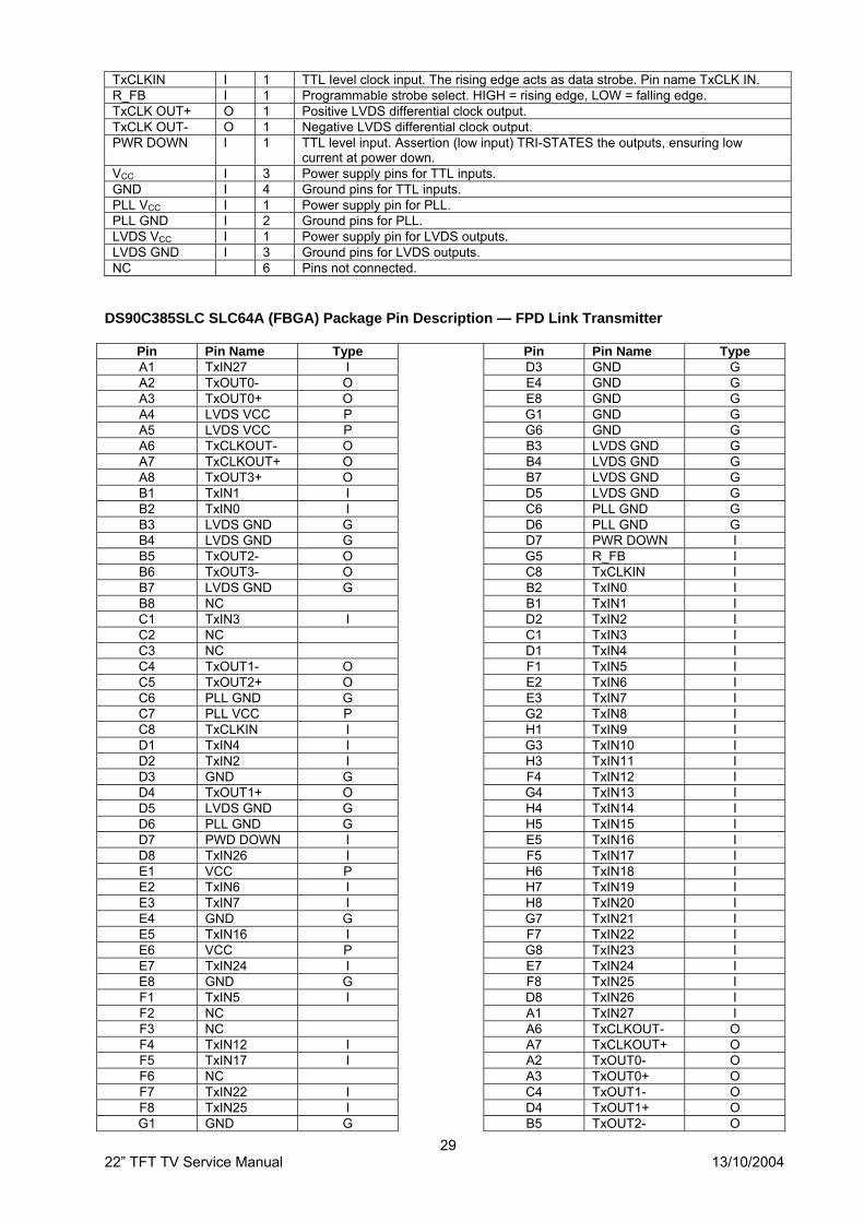
29 22” TFT TV Service Manual 13/10/2004
TxCLKIN I 1 TTL Ievel clock input. The rising edge acts as data strobe. Pin name TxCLK IN. R_FB I 1 Programmable strobe select. HIGH = rising edge, LOW = falling edge. TxCLK OUT+ O 1 Positive LVDS differential clock output. TxCLK OUT- O 1 Negative LVDS differential clock output. PWR DOWN I 1 TTL level input. Assertion (low input) TRI-STATES the outputs, ensuring low
current at power down. VCC I 3 Power supply pins for TTL inputs. GND I 4 Ground pins for TTL inputs. PLL VCC I 1 Power supply pin for PLL. PLL GND I 2 Ground pins for PLL. LVDS VCC I 1 Power supply pin for LVDS outputs. LVDS GND I 3 Ground pins for LVDS outputs. NC 6 Pins not connected.
DS90C385SLC SLC64A (FBGA) Package Pin Description — FPD Link Transmitter
Pin Pin Name Type Pin Pin Name Type A1 TxIN27 I D3 GND G A2 TxOUT0- O E4 GND G A3 TxOUT0+ O E8 GND G A4 LVDS VCC P G1 GND G A5 LVDS VCC P G6 GND G A6 TxCLKOUT- O B3 LVDS GND G A7 TxCLKOUT+ O B4 LVDS GND G A8 TxOUT3+ O B7 LVDS GND G B1 TxIN1 I D5 LVDS GND G B2 TxIN0 I C6 PLL GND G B3 LVDS GND G D6 PLL GND G B4 LVDS GND G D7 PWR DOWN I B5 TxOUT2- O G5 R_FB I B6 TxOUT3- O C8 TxCLKIN I B7 LVDS GND G B2 TxIN0 I B8 NC B1 TxIN1 I C1 TxIN3 I D2 TxIN2 I C2 NC C1 TxIN3 I C3 NC D1 TxIN4 I C4 TxOUT1- O F1 TxIN5 I C5 TxOUT2+ O E2 TxIN6 I C6 PLL GND G E3 TxIN7 I C7 PLL VCC P G2 TxIN8 I C8 TxCLKIN I H1 TxIN9 I D1 TxIN4 I G3 TxIN10 I D2 TxIN2 I H3 TxIN11 I D3 GND G F4 TxIN12 I D4 TxOUT1+ O G4 TxIN13 I D5 LVDS GND G H4 TxIN14 I D6 PLL GND G H5 TxIN15 I D7 PWD DOWN I E5 TxIN16 I D8 TxIN26 I F5 TxIN17 I E1 VCC P H6 TxIN18 I E2 TxIN6 I H7 TxIN19 I E3 TxIN7 I H8 TxIN20 I E4 GND G G7 TxIN21 I E5 TxIN16 I F7 TxIN22 I E6 VCC P G8 TxIN23 I E7 TxIN24 I E7 TxIN24 I E8 GND G F8 TxIN25 I F1 TxIN5 I D8 TxIN26 I F2 NC A1 TxIN27 I F3 NC A6 TxCLKOUT- O F4 TxIN12 I A7 TxCLKOUT+ O F5 TxIN17 I A2 TxOUT0- O F6 NC A3 TxOUT0+ O F7 TxIN22 I C4 TxOUT1- O F8 TxIN25 I D4 TxOUT1+ O G1 GND G B5 TxOUT2- O
30 22” TFT TV Service Manual 13/10/2004
G2 TxIN8 I C5 TxOUT2+ O G3 TxIN10 I B6 TxOUT3- O G4 TxIN13 I A8 TxOUT3+ O G5 R_FB I A4 LVDS VCC P G6 GND G A5 LVDS VCC P G7 TxIN21 I C7 PLL VCC P G8 TxIN23 I E1 VCC P H1 TxIN9 I E6 VCC P H2 VCC P H2 VCC P H3 TxIN11 I B8 NC H4 TxIN14 I C2 NC H5 TxIN15 I C3 NC H6 TxIN18 I F2 NC H7 TxIN19 I F3 NC H8 TxIN20 I F6 NC
G : Ground I : Input O : Output P : Power NC : No Connect DS90C365 Pin Description — FPD Link Transmitter
Pin name I/O No. Description TxIN I 21 TTL level input. This includes: 6 Red, 6 Green, 6 Blue, and 3 control lines —FPLINE,
FPFRAME and DRDY (also referred to as HSYNC, VSYNC, Data Enable). TxOUT+ O 3 Positive LVDS differentiaI data output. TxOUT- O 3 Negative LVDS differential data output. TxCLKIN I 1 TTL Ievel clock input. Pin name TxCLK IN. R_FB I 1 Programmable strobe select. TxCLK OUT+ O 1 Positive LVDS differential clock output. TxCLK OUT- O 1 Negative LVDS differential clock output. PWR DOWN I 1 TTL level input. Assertion (low input) TRI-STATES the outputs, ensuring low
current at power down. VCC I 3 Power supply pins for TTL inputs. GND I 4 Ground pins for TTL inputs. PLL VCC I 1 Power supply pin for PLL. PLL GND I 2 Ground pins for PLL. LVDS VCC I 1 Power supply pin for LVDS outputs. LVDS GND I 3 Ground pins for LVDS outputs.
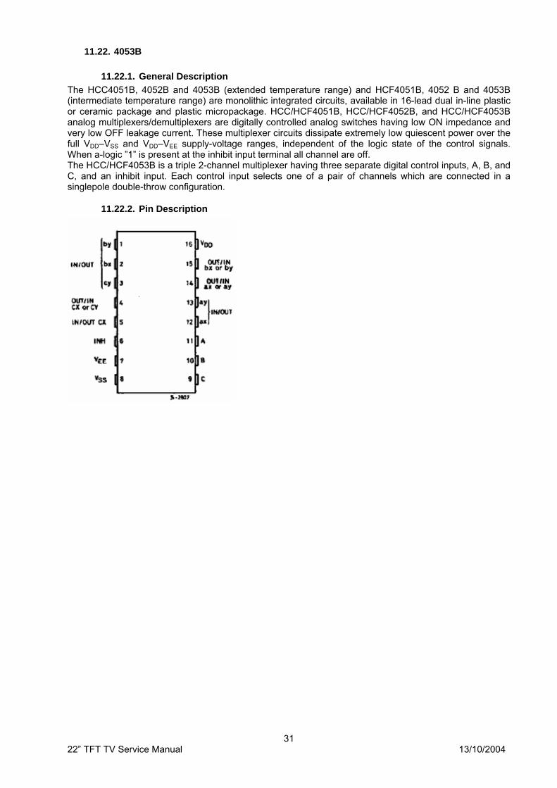
31 22” TFT TV Service Manual 13/10/2004
11.22. 4053B
11.22.1. General Description The HCC4051B, 4052B and 4053B (extended temperature range) and HCF4051B, 4052 B and 4053B (intermediate temperature range) are monolithic integrated circuits, available in 16-lead dual in-line plastic or ceramic package and plastic micropackage. HCC/HCF4051B, HCC/HCF4052B, and HCC/HCF4053B analog multiplexers/demultiplexers are digitally controlled analog switches having low ON impedance and very low OFF leakage current. These multiplexer circuits dissipate extremely low quiescent power over the full VDD–VSS and VDD–VEE supply-voltage ranges, independent of the logic state of the control signals. When a-logic ”1” is present at the inhibit input terminal all channel are off. The HCC/HCF4053B is a triple 2-channel multiplexer having three separate digital control inputs, A, B, and C, and an inhibit input. Each control input selects one of a pair of channels which are connected in a singlepole double-throw configuration.
11.22.2. Pin Description
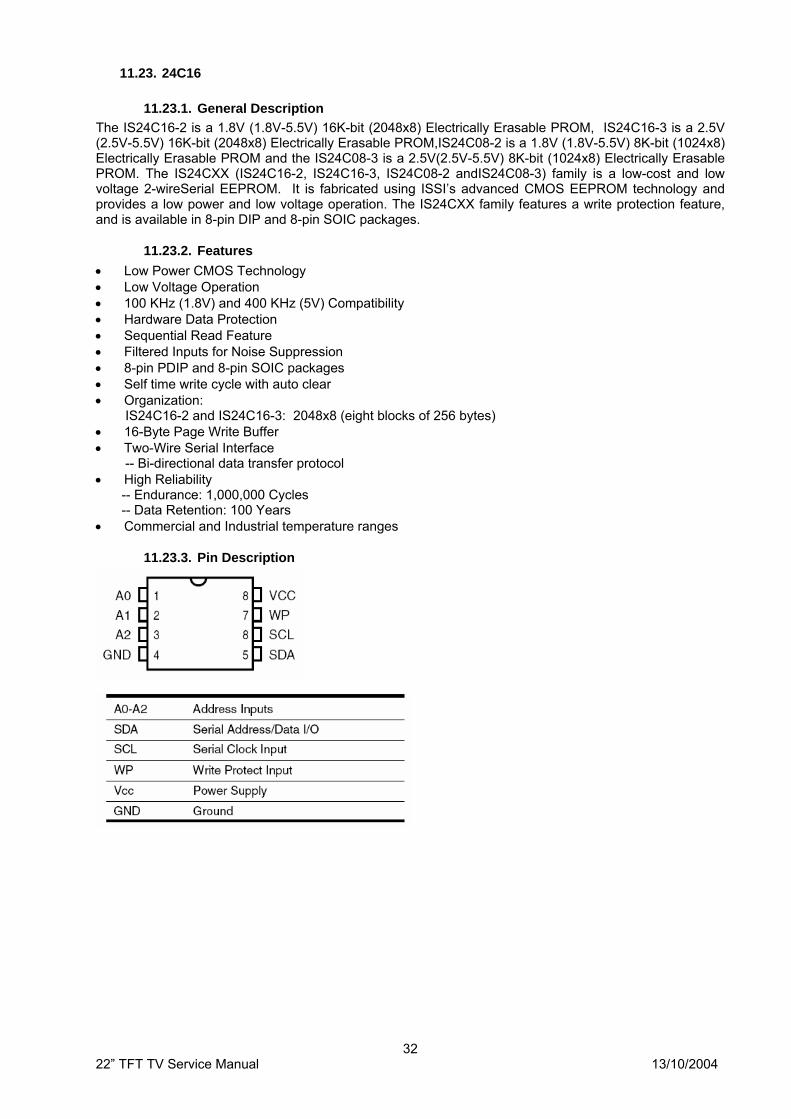
32 22” TFT TV Service Manual 13/10/2004
11.23. 24C16
11.23.1. General Description The IS24C16-2 is a 1.8V (1.8V-5.5V) 16K-bit (2048x8) Electrically Erasable PROM, IS24C16-3 is a 2.5V (2.5V-5.5V) 16K-bit (2048x8) Electrically Erasable PROM,IS24C08-2 is a 1.8V (1.8V-5.5V) 8K-bit (1024x8) Electrically Erasable PROM and the IS24C08-3 is a 2.5V(2.5V-5.5V) 8K-bit (1024x8) Electrically Erasable PROM. The IS24CXX (IS24C16-2, IS24C16-3, IS24C08-2 andIS24C08-3) family is a low-cost and low voltage 2-wireSerial EEPROM. It is fabricated using ISSI’s advanced CMOS EEPROM technology and provides a low power and low voltage operation. The IS24CXX family features a write protection feature, and is available in 8-pin DIP and 8-pin SOIC packages.
11.23.2. Features • Low Power CMOS Technology • Low Voltage Operation • 100 KHz (1.8V) and 400 KHz (5V) Compatibility • Hardware Data Protection • Sequential Read Feature • Filtered Inputs for Noise Suppression • 8-pin PDIP and 8-pin SOIC packages • Self time write cycle with auto clear • Organization: IS24C16-2 and IS24C16-3: 2048x8 (eight blocks of 256 bytes) • 16-Byte Page Write Buffer • Two-Wire Serial Interface -- Bi-directional data transfer protocol • High Reliability -- Endurance: 1,000,000 Cycles -- Data Retention: 100 Years • Commercial and Industrial temperature ranges
11.23.3. Pin Description
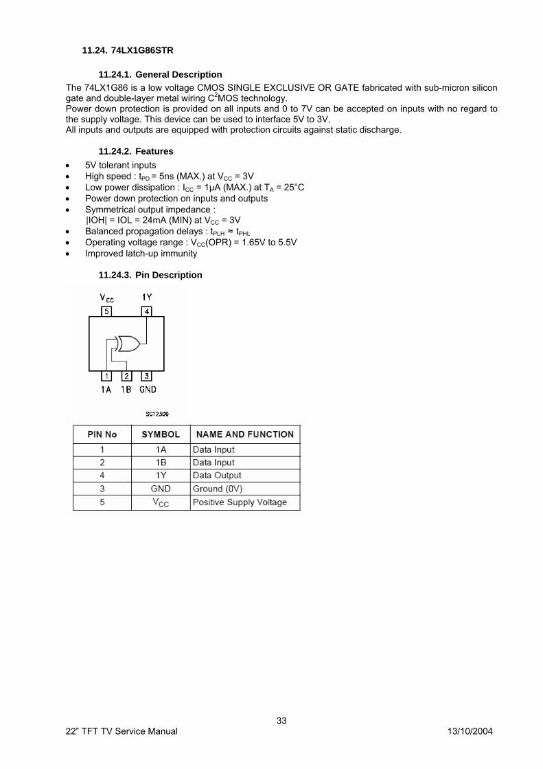
33 22” TFT TV Service Manual 13/10/2004
11.24. 74LX1G86STR
11.24.1. General Description The 74LX1G86 is a low voltage CMOS SINGLE EXCLUSIVE OR GATE fabricated with sub-micron silicon gate and double-layer metal wiring C2MOS technology. Power down protection is provided on all inputs and 0 to 7V can be accepted on inputs with no regard to the supply voltage. This device can be used to interface 5V to 3V. All inputs and outputs are equipped with protection circuits against static discharge.
11.24.2. Features • 5V tolerant inputs • High speed : tPD = 5ns (MAX.) at VCC = 3V • Low power dissipation : ICC = 1µA (MAX.) at TA = 25°C • Power down protection on inputs and outputs • Symmetrical output impedance : |IOH| = IOL = 24mA (MIN) at VCC = 3V • Balanced propagation delays : tPLH ≈ tPHL • Operating voltage range : VCC(OPR) = 1.65V to 5.5V • Improved latch-up immunity
11.24.3. Pin Description
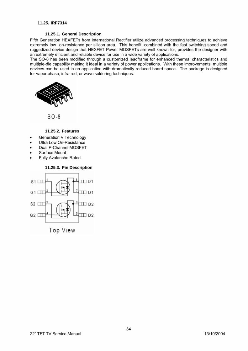
34 22” TFT TV Service Manual 13/10/2004
11.25. IRF7314
11.25.1. General Description Fifth Generation HEXFETs from International Rectifier utilize advanced processing techniques to achieve extremely low on-resistance per silicon area. This benefit, combined with the fast switching speed and ruggedized device design that HEXFET Power MOSFETs are well known for, provides the designer with an extremely efficient and reliable device for use in a wide variety of applications. The SO-8 has been modified through a customized leadframe for enhanced thermal characteristics and multiple-die capability making it ideal in a variety of power applications. With these improvements, multiple devices can be used in an application with dramatically reduced board space. The package is designed for vapor phase, infra red, or wave soldering techniques.
11.25.2. Features • Generation V Technology • Ultra Low On-Resistance • Dual P-Channel MOSFET • Surface Mount • Fully Avalanche Rated
11.25.3. Pin Description
35 22” TFT TV Service Manual 13/10/2004
12. IC DESCRIPTIONS (FOR DIGITAL)
STI5518 MX29LV160T MAX232_SMD 24C32
74HCU04 STV0360 TSH22 MAX809 CS4334 TDCC2345TV39A
AMIC A43L2616
12.1. STI5518
12.1.1. General Description The STi5518 is a highly integrated single-chip decoder, designed for use in feature-rich mass-market set-top boxes. It integrates a high-performance 32-bit CPU, a dedicated block for DVB/DirecTV transport demultiplexing and descrambling, modules for MPEG-2 video and audio decoding with 3D-surround and MP3 support, advanced display and graphics features, a digital video encoder and all of the system peripherals required in a typical low-cost interactive receiver. To cover the needs of DVD-capable set-top boxes, STi5518 integration options include a CSS decryption block, a Dolby Digital audio decoder and Macrovision copy protection. An ATAPI interface is built-in, supporting the glueless connection of standard Hard Disk Drives. In this way, the STi5518 is ideal for set-top boxes featuring trick modes such as live TV recording, pausing and time-shifting. The STi5518 is backward compatible with the popular STi5500 set-top box decoder, allowing easy migration from the previous generation. The high level of integration in a single PQFP-208 package makes the STi5518 ideally suited for low-cost, high-volume set-top box applications.
12.2. MAX232_SMD
12.2.1. General Description The MAX220–MAX249 family of line drivers/receivers is intended for all EIA/TIA-232E and V.28/V.24 communications interfaces, particularly applications where ±12V is not available. These parts are especially useful in battery-powered systems, since their low-power shutdown mode reduces power dissipation to less than 5µW. The MAX225, MAX233, MAX235, and MAX245/MAX246/MAX247 use no external components and are recommended for applications where printed circuit board space is critical.
12.2.2. Features • Operate from Single +5V Power Supply (+5V and +12V—MAX231/MAX239) • Low-Power Receive Mode in Shutdown (MAX223/MAX242) • Meet All EIA/TIA-232E and V.28 Specifications • Multiple Drivers and Receivers • 3-State Driver and Receiver Outputs • Open-Line Detection (MAX243)
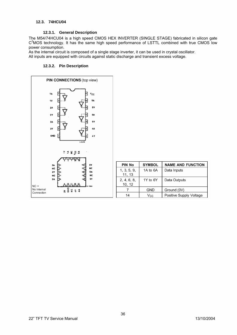
36 22” TFT TV Service Manual 13/10/2004
12.3. 74HCU04
12.3.1. General Description The M54/74HCU04 is a high speed CMOS HEX INVERTER (SINGLE STAGE) fabricated in silicon gate C2MOS technology. It has the same high speed performance of LSTTL combined with true CMOS low power consumption. As the internal circuit is composed of a single stage inverter, it can be used in crystal oscillator. All inputs are equipped with circuits against static discharge and transient excess voltage.
12.3.2. Pin Description
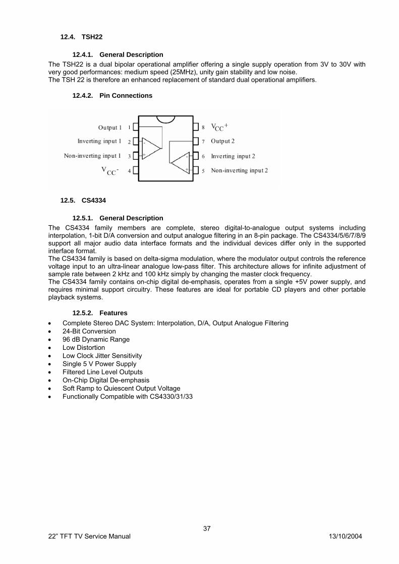
37 22” TFT TV Service Manual 13/10/2004
12.4. TSH22
12.4.1. General Description The TSH22 is a dual bipolar operational amplifier offering a single supply operation from 3V to 30V with very good performances: medium speed (25MHz), unity gain stability and low noise. The TSH 22 is therefore an enhanced replacement of standard dual operational amplifiers.
12.4.2. Pin Connections
12.5. CS4334
12.5.1. General Description The CS4334 family members are complete, stereo digital-to-analogue output systems including interpolation, 1-bit D/A conversion and output analogue filtering in an 8-pin package. The CS4334/5/6/7/8/9 support all major audio data interface formats and the individual devices differ only in the supported interface format. The CS4334 family is based on delta-sigma modulation, where the modulator output controls the reference voltage input to an ultra-linear analogue low-pass filter. This architecture allows for infinite adjustment of sample rate between 2 kHz and 100 kHz simply by changing the master clock frequency. The CS4334 family contains on-chip digital de-emphasis, operates from a single +5V power supply, and requires minimal support circuitry. These features are ideal for portable CD players and other portable playback systems.
12.5.2. Features • Complete Stereo DAC System: Interpolation, D/A, Output Analogue Filtering • 24-Bit Conversion • 96 dB Dynamic Range • Low Distortion • Low Clock Jitter Sensitivity • Single 5 V Power Supply • Filtered Line Level Outputs • On-Chip Digital De-emphasis • Soft Ramp to Quiescent Output Voltage • Functionally Compatible with CS4330/31/33
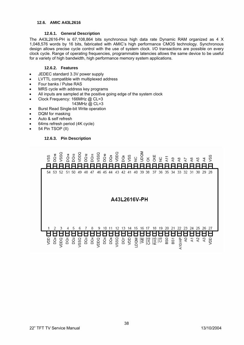
38 22” TFT TV Service Manual 13/10/2004
12.6. AMIC A43L2616
12.6.1. General Description The A43L2616-PH is 67,108,864 bits synchronous high data rate Dynamic RAM organized as 4 X 1,048,576 words by 16 bits, fabricated with AMIC’s high performance CMOS technology. Synchronous design allows precise cycle control with the use of system clock. I/O transactions are possible on every clock cycle. Range of operating frequencies, programmable latencies allows the same device to be useful for a variety of high bandwidth, high performance memory system applications.
12.6.2. Features • JEDEC standard 3.3V power supply • LVTTL compatible with multiplexed address • Four banks / Pulse RAS • MRS cycle with address key programs • All inputs are sampled at the positive going edge of the system clock • Clock Frequency: 166MHz @ CL=3 143MHz @ CL=3 • Burst Read Single-bit Write operation • DQM for masking • Auto & self refresh • 64ms refresh period (4K cycle) • 54 Pin TSOP (II)
12.6.3. Pin Description
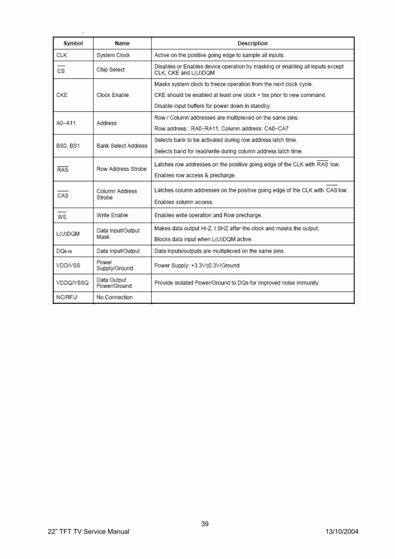
39 22” TFT TV Service Manual 13/10/2004
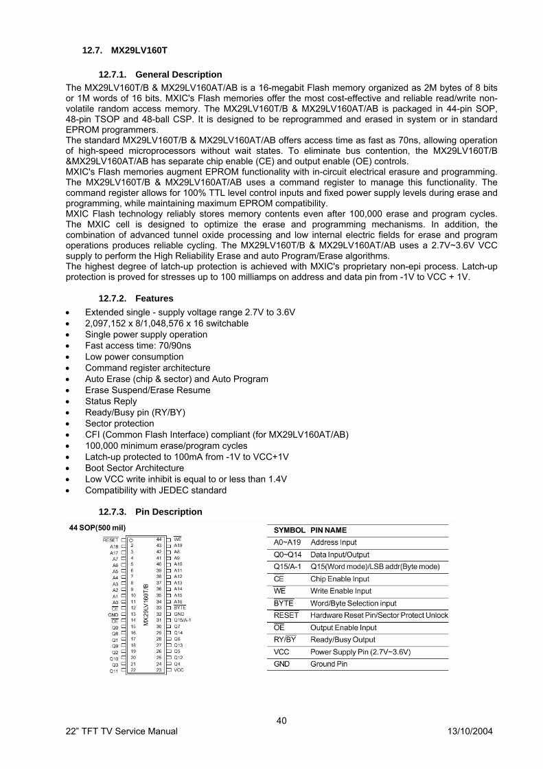
40 22” TFT TV Service Manual 13/10/2004
12.7. MX29LV160T
12.7.1. General Description The MX29LV160T/B & MX29LV160AT/AB is a 16-megabit Flash memory organized as 2M bytes of 8 bits or 1M words of 16 bits. MXIC's Flash memories offer the most cost-effective and reliable read/write non-volatile random access memory. The MX29LV160T/B & MX29LV160AT/AB is packaged in 44-pin SOP, 48-pin TSOP and 48-ball CSP. It is designed to be reprogrammed and erased in system or in standard EPROM programmers. The standard MX29LV160T/B & MX29LV160AT/AB offers access time as fast as 70ns, allowing operation of high-speed microprocessors without wait states. To eliminate bus contention, the MX29LV160T/B &MX29LV160AT/AB has separate chip enable (CE) and output enable (OE) controls. MXIC's Flash memories augment EPROM functionality with in-circuit electrical erasure and programming. The MX29LV160T/B & MX29LV160AT/AB uses a command register to manage this functionality. The command register allows for 100% TTL level control inputs and fixed power supply levels during erase and programming, while maintaining maximum EPROM compatibility. MXIC Flash technology reliably stores memory contents even after 100,000 erase and program cycles. The MXIC cell is designed to optimize the erase and programming mechanisms. In addition, the combination of advanced tunnel oxide processing and low internal electric fields for erase and program operations produces reliable cycling. The MX29LV160T/B & MX29LV160AT/AB uses a 2.7V~3.6V VCC supply to perform the High Reliability Erase and auto Program/Erase algorithms. The highest degree of latch-up protection is achieved with MXIC's proprietary non-epi process. Latch-up protection is proved for stresses up to 100 milliamps on address and data pin from -1V to VCC + 1V.
12.7.2. Features • Extended single - supply voltage range 2.7V to 3.6V • 2,097,152 x 8/1,048,576 x 16 switchable • Single power supply operation • Fast access time: 70/90ns • Low power consumption • Command register architecture • Auto Erase (chip & sector) and Auto Program • Erase Suspend/Erase Resume • Status Reply • Ready/Busy pin (RY/BY) • Sector protection • CFI (Common Flash Interface) compliant (for MX29LV160AT/AB) • 100,000 minimum erase/program cycles • Latch-up protected to 100mA from -1V to VCC+1V • Boot Sector Architecture • Low VCC write inhibit is equal to or less than 1.4V • Compatibility with JEDEC standard
12.7.3. Pin Description
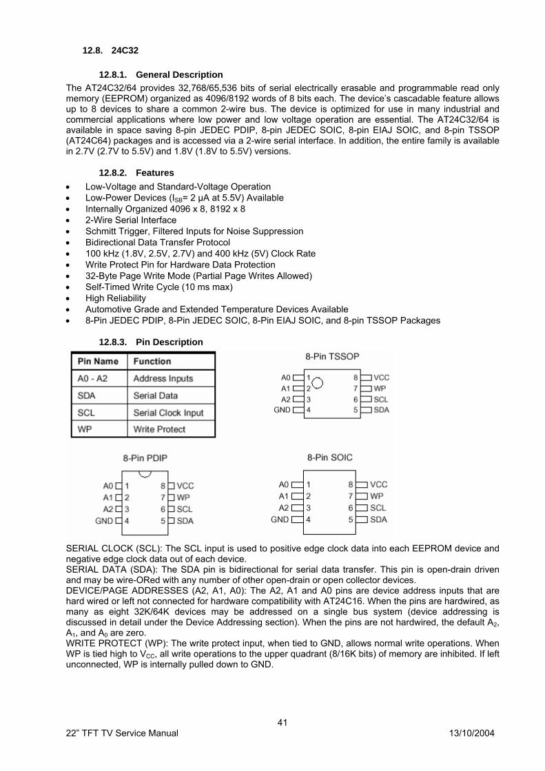
41 22” TFT TV Service Manual 13/10/2004
12.8. 24C32
12.8.1. General Description The AT24C32/64 provides 32,768/65,536 bits of serial electrically erasable and programmable read only memory (EEPROM) organized as 4096/8192 words of 8 bits each. The device’s cascadable feature allows up to 8 devices to share a common 2-wire bus. The device is optimized for use in many industrial and commercial applications where low power and low voltage operation are essential. The AT24C32/64 is available in space saving 8-pin JEDEC PDIP, 8-pin JEDEC SOIC, 8-pin EIAJ SOIC, and 8-pin TSSOP (AT24C64) packages and is accessed via a 2-wire serial interface. In addition, the entire family is available in 2.7V (2.7V to 5.5V) and 1.8V (1.8V to 5.5V) versions.
12.8.2. Features • Low-Voltage and Standard-Voltage Operation • Low-Power Devices (ISB= 2 µA at 5.5V) Available • Internally Organized 4096 x 8, 8192 x 8 • 2-Wire Serial Interface • Schmitt Trigger, Filtered Inputs for Noise Suppression • Bidirectional Data Transfer Protocol • 100 kHz (1.8V, 2.5V, 2.7V) and 400 kHz (5V) Clock Rate • Write Protect Pin for Hardware Data Protection • 32-Byte Page Write Mode (Partial Page Writes Allowed) • Self-Timed Write Cycle (10 ms max) • High Reliability • Automotive Grade and Extended Temperature Devices Available • 8-Pin JEDEC PDIP, 8-Pin JEDEC SOIC, 8-Pin EIAJ SOIC, and 8-pin TSSOP Packages
12.8.3. Pin Description
SERIAL CLOCK (SCL): The SCL input is used to positive edge clock data into each EEPROM device and negative edge clock data out of each device. SERIAL DATA (SDA): The SDA pin is bidirectional for serial data transfer. This pin is open-drain driven and may be wire-ORed with any number of other open-drain or open collector devices. DEVICE/PAGE ADDRESSES (A2, A1, A0): The A2, A1 and A0 pins are device address inputs that are hard wired or left not connected for hardware compatibility with AT24C16. When the pins are hardwired, as many as eight 32K/64K devices may be addressed on a single bus system (device addressing is discussed in detail under the Device Addressing section). When the pins are not hardwired, the default A2, A1, and A0 are zero. WRITE PROTECT (WP): The write protect input, when tied to GND, allows normal write operations. When WP is tied high to VCC, all write operations to the upper quadrant (8/16K bits) of memory are inhibited. If left unconnected, WP is internally pulled down to GND.
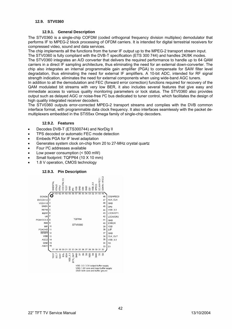
42 22” TFT TV Service Manual 13/10/2004
12.9. STV0360
12.9.1. General Description The STV0360 is a single-chip COFDM (coded orthogonal frequency division multiplex) demodulator that performs IF to MPEG-2 block processing of OFDM carriers. It is intended for digital terrestrial receivers for compressed video, sound and data services. The chip implements all the functions from the tuner IF output up to the MPEG-2 transport stream input. The STV0360 is fully compliant with the DVB-T specification (ETS 300 744) and handles 2K/8K modes. The STV0360 integrates an A/D converter that delivers the required performance to handle up to 64 QAM carriers in a direct IF sampling architecture, thus eliminating the need for an external down-converter. The chip also integrates an internal programmable gain amplifier (PGA) to compensate for SAW filter level degradation, thus eliminating the need for external IF amplifiers. A 10-bit ADC, intended for RF signal strength indication, eliminates the need for external components when using wide-band AGC tuners. In addition to all the demodulation and FEC (forward error correction) functions required for recovery of the QAM modulated bit streams with very low BER, it also includes several features that give easy and immediate access to various quality monitoring parameters or lock status. The STV0360 also provides output such as delayed AGC or noise-free I²C bus dedicated to tuner control, which facilitates the design of high quality integrated receiver decoders. The STV0360 outputs error-corrected MPEG-2 transport streams and complies with the DVB common interface format, with programmable data clock frequency. It also interfaces seamlessly with the packet de-multiplexers embedded in the STi55xx Omega family of single-chip decoders.
12.9.2. Features • Decodes DVB-T (ETS300744) and NorDig II • TPS decoded or automatic FEC mode detection • Embeds PGA for IF level adaptation • Generates system clock on-chip from 20 to 27-MHz crystal quartz • Four I²C addresses available • Low power consumption (< 500 mW) • Small footprint: TQFP64 (10 X 10 mm) • 1.8 V operation, CMOS technology
12.9.3. Pin Description
43 22” TFT TV Service Manual 13/10/2004
44 22” TFT TV Service Manual 13/10/2004
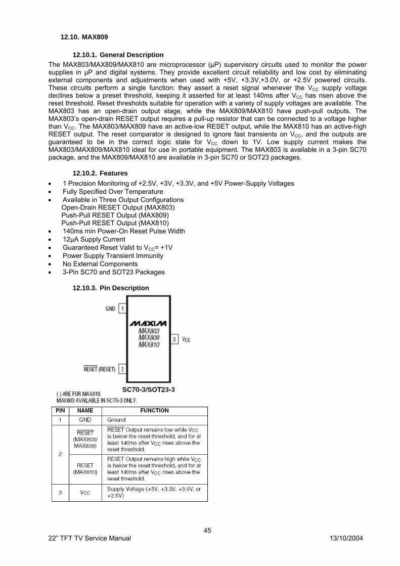
45 22” TFT TV Service Manual 13/10/2004
12.10. MAX809
12.10.1. General Description The MAX803/MAX809/MAX810 are microprocessor (µP) supervisory circuits used to monitor the power supplies in µP and digital systems. They provide excellent circuit reliability and low cost by eliminating external components and adjustments when used with +5V, +3.3V,+3.0V, or +2.5V powered circuits. These circuits perform a single function: they assert a reset signal whenever the VCC supply voltage declines below a preset threshold, keeping it asserted for at least 140ms after VCC has risen above the reset threshold. Reset thresholds suitable for operation with a variety of supply voltages are available. The MAX803 has an open-drain output stage, while the MAX809/MAX810 have push-pull outputs. The MAX803’s open-drain RESET output requires a pull-up resistor that can be connected to a voltage higher than VCC. The MAX803/MAX809 have an active-low RESET output, while the MAX810 has an active-high RESET output. The reset comparator is designed to ignore fast transients on VCC, and the outputs are guaranteed to be in the correct logic state for VCC down to 1V. Low supply current makes the MAX803/MAX809/MAX810 ideal for use in portable equipment. The MAX803 is available in a 3-pin SC70 package, and the MAX809/MAX810 are available in 3-pin SC70 or SOT23 packages.
12.10.2. Features • 1 Precision Monitoring of +2.5V, +3V, +3.3V, and +5V Power-Supply Voltages • Fully Specified Over Temperature • Available in Three Output Configurations Open-Drain RESET Output (MAX803) Push-Pull RESET Output (MAX809) Push-Pull RESET Output (MAX810) • 140ms min Power-On Reset Pulse Width • 12µA Supply Current • Guaranteed Reset Valid to VCC= +1V • Power Supply Transient Immunity • No External Components • 3-Pin SC70 and SOT23 Packages
12.10.3. Pin Description
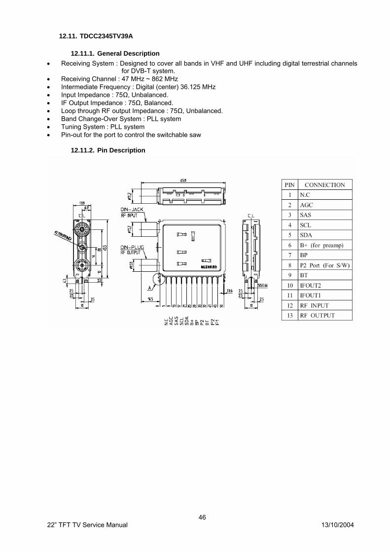
46 22” TFT TV Service Manual 13/10/2004
12.11. TDCC2345TV39A
12.11.1. General Description • Receiving System : Designed to cover all bands in VHF and UHF including digital terrestrial channels
for DVB-T system. • Receiving Channel : 47 MHz ~ 862 MHz • Intermediate Frequency : Digital (center) 36.125 MHz • Input Impedance : 75Ω, Unbalanced. • IF Output Impedance : 75Ω, Balanced. • Loop through RF output Impedance : 75Ω, Unbalanced. • Band Change-Over System : PLL system • Tuning System : PLL system • Pin-out for the port to control the switchable saw
12.11.2. Pin Description
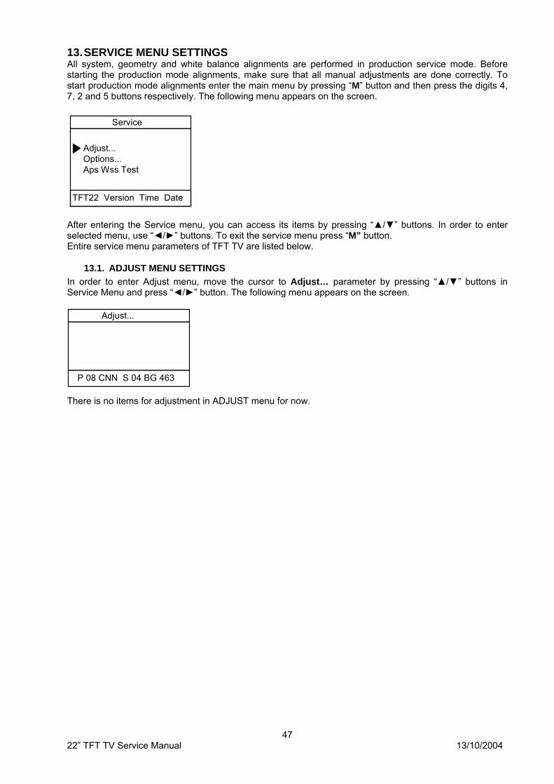
47 22” TFT TV Service Manual 13/10/2004
13. SERVICE MENU SETTINGS All system, geometry and white balance alignments are performed in production service mode. Before starting the production mode alignments, make sure that all manual adjustments are done correctly. To start production mode alignments enter the main menu by pressing “M” button and then press the digits 4, 7, 2 and 5 buttons respectively. The following menu appears on the screen. After entering the Service menu, you can access its items by pressing “/” buttons. In order to enter selected menu, use “/” buttons. To exit the service menu press “M” button. Entire service menu parameters of TFT TV are listed below.
13.1. ADJUST MENU SETTINGS In order to enter Adjust menu, move the cursor to Adjust… parameter by pressing “/” buttons in Service Menu and press “/” button. The following menu appears on the screen. There is no items for adjustment in ADJUST menu for now.
Adjust...
P 08 CNN S 04 BG 463
Service
Adjust...Options...Aps Wss Test
TFT22 Version Time Date
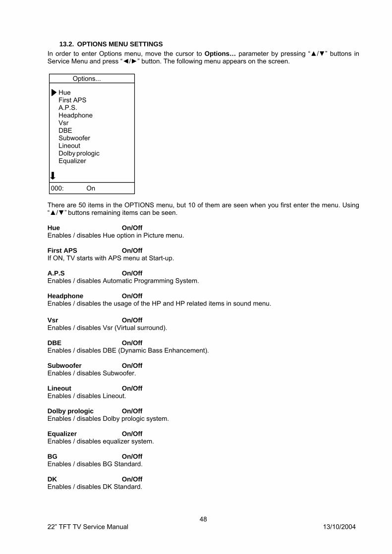
48 22” TFT TV Service Manual 13/10/2004
13.2. OPTIONS MENU SETTINGS In order to enter Options menu, move the cursor to Options… parameter by pressing “/” buttons in Service Menu and press “/” button. The following menu appears on the screen. There are 50 items in the OPTIONS menu, but 10 of them are seen when you first enter the menu. Using “/” buttons remaining items can be seen. Hue On/Off Enables / disables Hue option in Picture menu. First APS On/Off If ON, TV starts with APS menu at Start-up. A.P.S On/Off Enables / disables Automatic Programming System. Headphone On/Off Enables / disables the usage of the HP and HP related items in sound menu. Vsr On/Off Enables / disables Vsr (Virtual surround). DBE On/Off Enables / disables DBE (Dynamic Bass Enhancement). Subwoofer On/Off Enables / disables Subwoofer. Lineout On/Off Enables / disables Lineout. Dolby prologic On/Off Enables / disables Dolby prologic system. Equalizer On/Off Enables / disables equalizer system. BG On/Off Enables / disables BG Standard. DK On/Off Enables / disables DK Standard.
Options...
Hue First APS A.P.S. Headphone Vsr DBE Subwoofer Lineout Dolby prologic Equalizer
000: On
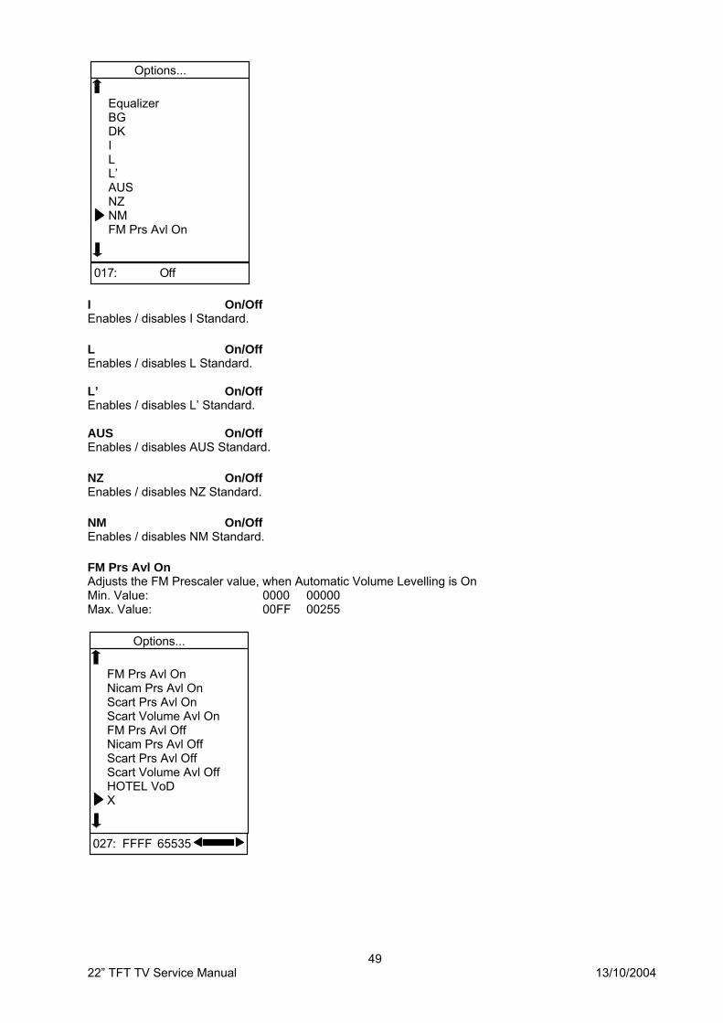
49 22” TFT TV Service Manual 13/10/2004
I On/Off Enables / disables I Standard. L On/Off Enables / disables L Standard. L’ On/Off Enables / disables L’ Standard. AUS On/Off Enables / disables AUS Standard. NZ On/Off Enables / disables NZ Standard. NM On/Off Enables / disables NM Standard. FM Prs Avl On Adjusts the FM Prescaler value, when Automatic Volume Levelling is On Min. Value: 0000 00000 Max. Value: 00FF 00255
Options...
Equalizer BG DK I L L’ AUS NZ NM FM Prs Avl On
0 17 : O ff
Options...
FM Prs Avl On Nicam Prs Avl On Scart Prs Avl On Scart Volume Avl OnFM Prs Avl Off Nicam Prs Avl Off Scart Prs Avl Off Scart Volume Avl OffHOTEL VoD X
0 27 : FFFF 65535
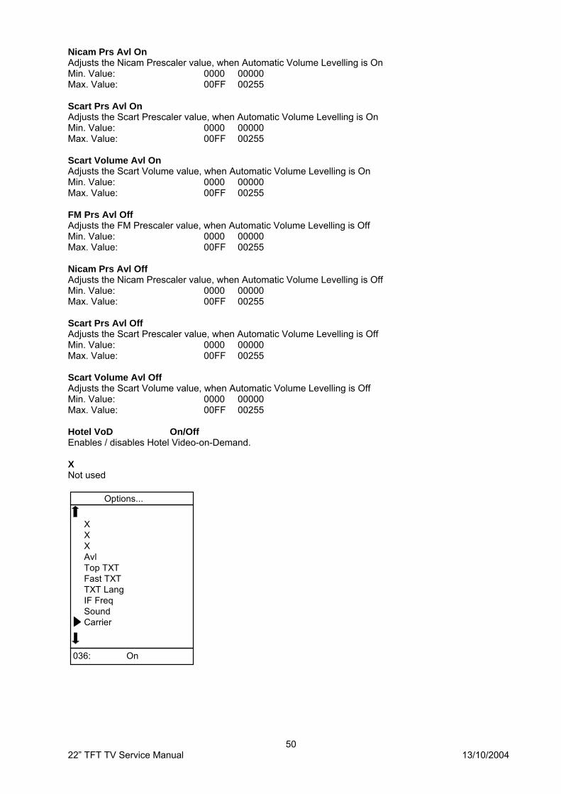
50 22” TFT TV Service Manual 13/10/2004
Nicam Prs Avl On Adjusts the Nicam Prescaler value, when Automatic Volume Levelling is On Min. Value: 0000 00000 Max. Value: 00FF 00255 Scart Prs Avl On Adjusts the Scart Prescaler value, when Automatic Volume Levelling is On Min. Value: 0000 00000 Max. Value: 00FF 00255 Scart Volume Avl On Adjusts the Scart Volume value, when Automatic Volume Levelling is On Min. Value: 0000 00000 Max. Value: 00FF 00255 FM Prs Avl Off Adjusts the FM Prescaler value, when Automatic Volume Levelling is Off Min. Value: 0000 00000 Max. Value: 00FF 00255 Nicam Prs Avl Off Adjusts the Nicam Prescaler value, when Automatic Volume Levelling is Off Min. Value: 0000 00000 Max. Value: 00FF 00255 Scart Prs Avl Off Adjusts the Scart Prescaler value, when Automatic Volume Levelling is Off Min. Value: 0000 00000 Max. Value: 00FF 00255 Scart Volume Avl Off Adjusts the Scart Volume value, when Automatic Volume Levelling is Off Min. Value: 0000 00000 Max. Value: 00FF 00255 Hotel VoD On/Off Enables / disables Hotel Video-on-Demand. X Not used
Options...
XXXAvlTop TXTFast TXTTXT LangIF FreqSoundCarrier
036: On
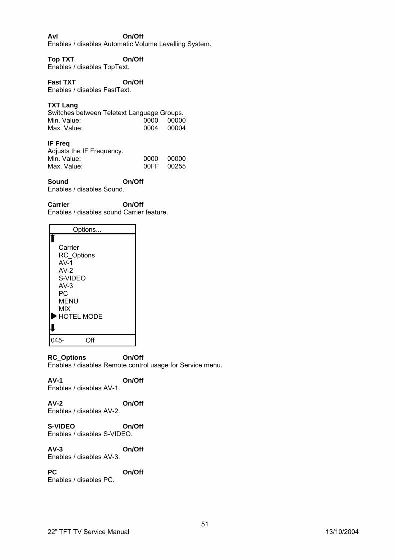
51 22” TFT TV Service Manual 13/10/2004
Avl On/Off Enables / disables Automatic Volume Levelling System. Top TXT On/Off Enables / disables TopText. Fast TXT On/Off Enables / disables FastText. TXT Lang Switches between Teletext Language Groups. Min. Value: 0000 00000 Max. Value: 0004 00004 IF Freq Adjusts the IF Frequency. Min. Value: 0000 00000 Max. Value: 00FF 00255 Sound On/Off Enables / disables Sound. Carrier On/Off Enables / disables sound Carrier feature. RC_Options On/Off Enables / disables Remote control usage for Service menu. AV-1 On/Off Enables / disables AV-1. AV-2 On/Off Enables / disables AV-2. S-VIDEO On/Off Enables / disables S-VIDEO. AV-3 On/Off Enables / disables AV-3. PC On/Off Enables / disables PC.
Options...
Carrier RC_Options AV - 1 AV - 2 S - VIDEO AV - 3 PC MENU MIX HOTEL MODE
0 45 - Off
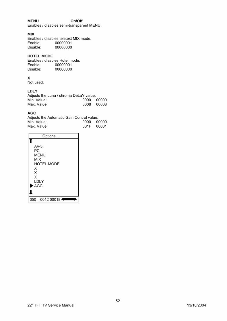
52 22” TFT TV Service Manual 13/10/2004
MENU On/Off Enables / disables semi-transparent MENU. MIX Enables / disables teletext MIX mode. Enable: 00000001 Disable: 00000000 HOTEL MODE Enables / disables Hotel mode. Enable: 00000001 Disable: 00000000 X Not used. LDLY Adjusts the Luna / chroma DeLaY value. Min. Value: 0000 00000 Max. Value: 0008 00008 AGC Adjusts the Automatic Gain Control value. Min. Value: 0000 00000 Max. Value: 001F 00031
Options...
AV - 3 PC MENU MIX HOTEL MODE X X X LDLY AGC
0 50 - 0012 00018
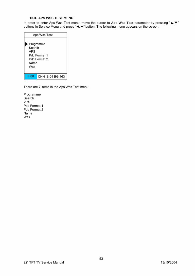
53 22” TFT TV Service Manual 13/10/2004
13.3. APS WSS TEST MENU In order to enter Aps Wss Test menu, move the cursor to Aps Wss Test parameter by pressing “/” buttons in Service Menu and press “/” button. The following menu appears on the screen. There are 7 items in the Aps Wss Test menu. Programme Search VPS Pdc Format 1 Pdc Format 2 Name Wss
Aps Wss Test
ProgrammeSearchVPSPdc Format 1Pdc Format 2NameWss
CNN S 04 BG 463P 08
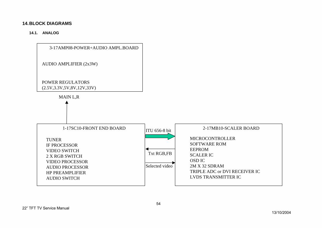
54 22” TFT TV Service Manual 13/10/2004
14. BLOCK DIAGRAMS
14.1. ANALOG
1-17SC10 - FRONT END BOARD 2-17MB10-SCALER BOARD
3-17AMP08 - POWER+AUDIO AMPL.BOARD
ITU 656-8 bit
Txt RGB,FB
MAIN L,R
POWER REGULATORS (2.5V,3.3V,5V,8V,12V,33V)
AUDIO AMPLIFIER (2x3W)
TUNER IF PROCESSOR VIDEO SWITCH 2 X RGB SWITCH VIDEO PROCESSOR AUDIO PROCESSOR HP PREAMPLIFIER AUDIO SWITCH
MICROCONTROLLERSOFTWARE ROMEEPROMSCALER IC OSD IC2M X 32 SDRAMTRIPLE ADC or DVI RECEIVER ICLVDS TRANSMITTER IC
Selected video
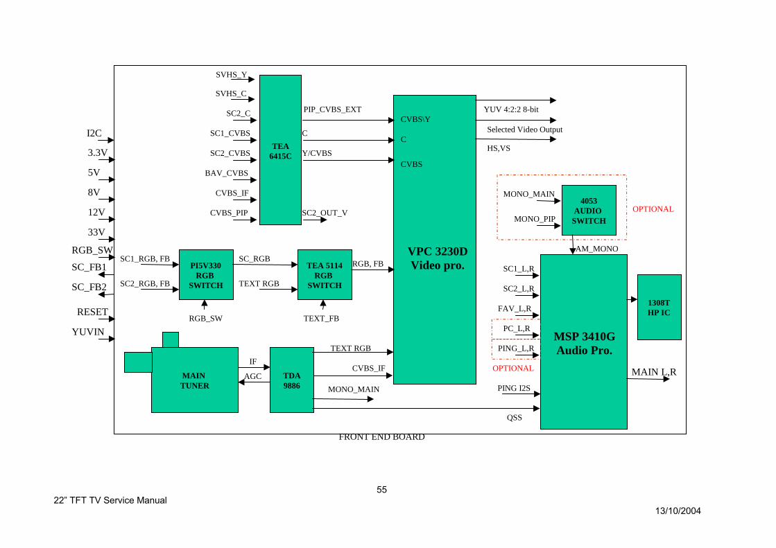
55 22” TFT TV Service Manual 13/10/2004
FRONT END BOARD
TEA6415C
SVHS_Y
SVHS_C
SC1_CVBS
SC2_C
BAV_CVBS
SC2_CVBS
C
CVBS\Y
TEXT RGB
Selected Video Output
SC1_RGB, FB
YUV 4:2:2 8-bit
CVBS_PIP
CVBS_IF
SC2_OUT_V
C
Y/CVBS
PIP_CVBS_EXT
MAIN TUNER
CVBS_IF
CVBS
TDA9886
IF
VPC 3230DVideo pro.PI5V330
RGB SWITCHSC2_RGB, FB
RGB_SW
SC_RGBTEA 5114
RGB SWITCH
TEXT_FB
RGB, FB
TEXT RGBMSP 3410GAudio Pro.
QSS
SC1_L,R
SC2_L,R
FAV_L,R
PC_L,R
MONO_MAIN4053
AUDIO SWITCHMONO_PIP
AM_MONO
1308THP IC
MAIN L,R
OPTIONAL
MONO_MAIN
PING_L,R
OPTIONAL
PING I2S
I2C
3.3V
5V
8V
12V
33V
RGB_SW
RESET
YUVIN
SC_FB1
AGC
HS,VS
SC_FB2
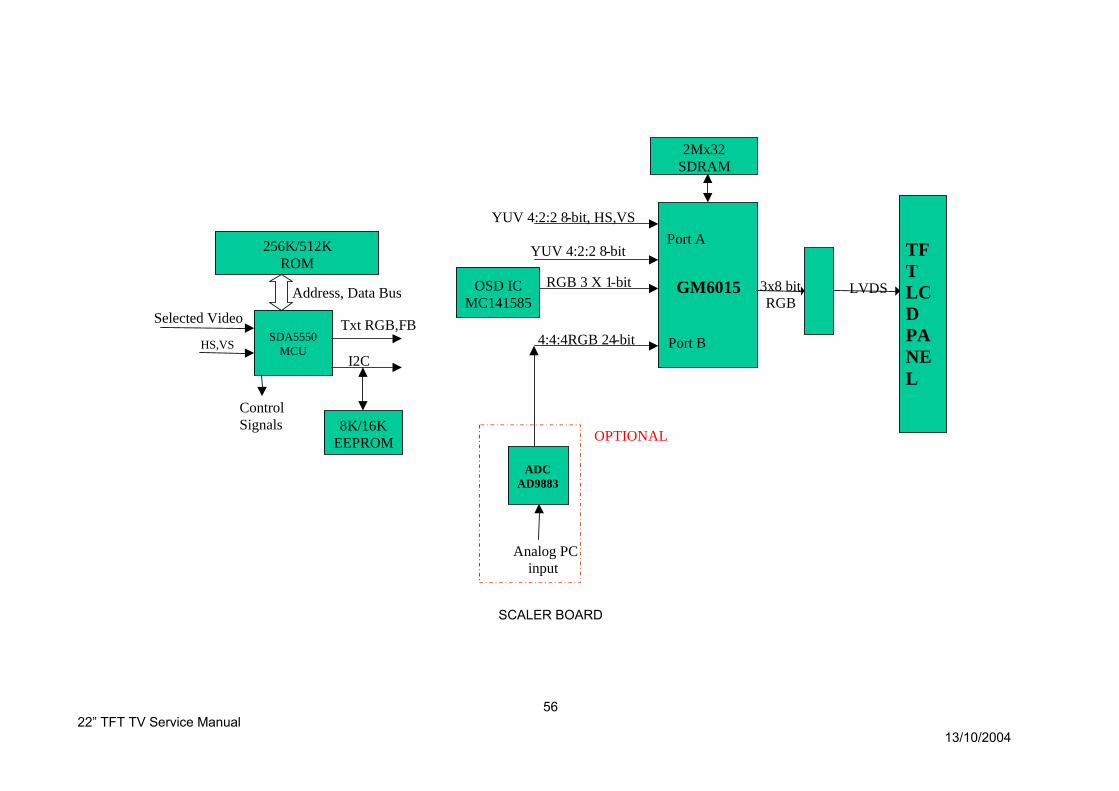
56 22” TFT TV Service Manual 13/10/2004
SCALER BOARD
GM6015
Port A
Port B
2Mx32SDRAM
ADCAD9883
YUV 4:2:2 8-bit
YUV 4:2:2 8-bit, HS,VS
SDA5550MCU
4:4:4RGB 24-bit
3x8 bitRGB
TFT LCD PANEL
Selected Video Txt RGB,FB
I2C
256K/512KROM
Address, Data Bus
8K/16KEEPROM
ControlSignals
Analog PCinput
RGB 3 X 1-bitOSD ICMC141585
OPTIONAL
HS,VS
LVDS
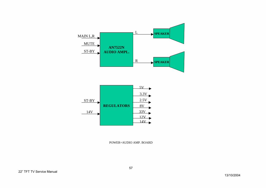
57 22” TFT TV Service Manual 13/10/2004
POWER+AUDIO AMP. BOARD
AN7522NAUDIO AMPL.
MAIN L,R
MUTE
ST-BY
SPEAKERL
SPEAKERR
REGULATORSST-BY
14V
5V
3.3V2.5V8V33V12V14V

58 22” TFT TV Service Manual 13/10/2004
14.2. DIGITAL

59 22” TFT TV Service Manual 13/10/2004
15. CIRCUIT DIAGRAMS
15.1. ANALOG
17AMP08 001

60 22” TFT TV Service Manual 13/10/2004
17AMP08 002

61 22” TFT TV Service Manual 13/10/2004
17MB10 001

62 22” TFT TV Service Manual 13/10/2004
17MB10 002

63 22” TFT TV Service Manual 13/10/2004
17MB10 003

64 22” TFT TV Service Manual 13/10/2004
17SC10-1 001

65 22” TFT TV Service Manual 13/10/2004
17SC10-1 002

66 22” TFT TV Service Manual 13/10/2004
17SC10-1 003

67 22” TFT TV Service Manual 13/10/2004
17SC10-1 004

68 22” TFT TV Service Manual 13/10/2004
15.2. DIGITAL

69 22” TFT TV Service Manual 13/10/2004

70 22” TFT TV Service Manual 13/10/2004

71 22” TFT TV Service Manual 13/10/2004

72 22” TFT TV Service Manual 13/10/2004

73 22” TFT TV Service Manual 13/10/2004

74 22” TFT TV Service Manual 13/10/2004