Embed Size (px)
Citation preview

Elsevier Science 1
Technical challenges and recent progress in CCD imagersJan T. Bosiersa*, Inge M. Petersa, Cees Draijera, Albert Theuwissenb
aDALSA Professional Imaging, High Tech Campus 12a, M/S 01 (WAD01), 5656 AE Eindhoven, The Netherlands
bDALSA Digital Imaging, High Tech Campus 12a, M/S 01 (WAD01), 5656 AE Eindhoven, The Netherlands
Elsevier use only: Received date here; revised date here; accepted date here
Abstract
This paper gives a review of the performance of CCD imagers for use in consumer, professional and scientific applications. An overview of recent developments and the current state-of-the-art are presented. An extensive list of references is included.
© 2001 Elsevier Science. All rights reserved
Keywords; CCD, imagingPACS: the PACS codes can be found at the home page of NIMA (left column, under Contents Services): http://www.elsevier.nl/inca/publications/store/5/0/5/7/0/1/
* Corresponding author. Tel.: +31-40-274 22 27; fax: +31-40-274 40 90; e-mail: [email protected]

Elsevier Science2
n-substrate
p-well
n- p+p+
channel stop
Poly-Si gate
oxide
A1
A2
A3
A4
A1
channel stops
Introduction
The purpose of using a charge-coupled device (CCD) imager in any application is to obtain a clear image of a scene with a sufficiently high signal-to-noise ratio (SNR) under given exposure conditions at a competitive cost.
This paper will give several examples from different application areas showing that CCDs continue to meet increasing demands: increasing resolution and speed, lower light levels, smaller pixel sizes, larger focal plane areas, etc. All three basic CCD imager concepts (frame transfer, full frame and interline transfer) will be reviewed.
First, the advancement of technologies and design concepts for CCD imagers will be discussed for consumer, professional and industrial imaging. Then the status, challenges and recent progress in CCD imagers for scientific imaging will be extensively reviewed.
1. Basic CCD architectures
For convenience, we will distinguish between four different CCD imager concepts: interline-transfer, frame-transfer and full-frame CCDs and ‘others’ [1].� In an interline-transfer CCD (IL-CCD), each
pixel consists of a photodiode and one cell of a CCD register. The array of photodiodes converts incident photons to electron-hole pairs. After exposure, the collected electrons are transferred from the photodiode to the adjacent CCD readout registers (‘vertical’ registers). For readout, the charge from the vertical registers is transferred line-by-line to the ‘horizontal’ register for readout through the output amplifier. Fig. 1 shows a typical cross-section of an IL-CCD pixel and adjacent vertical CCD register.
� In a full-frame CCD (FF-CCD), photon-detection, charge integration and charge transport are all done in the same area of the pixel. After exposure, the sensor needs to be shielded from light for readout. Fig. 2 shows a typical top view and cross-section of a FF-CCD pixel.
� The pixel array of frame-transfer CCD (FT-CCD) is similar to that of a FF-CCD. After exposure, the collected charge packets are transferred to a storage section where they are shielded from light.
� Other more ‘exotic’ CCD imager concepts and architectures will be discussed later.
Fig.1. Typical IL-CCD pixel. (PD=photodiode, TG=transfer gate,
CS=channel stop, V-CCD= vertical interline CCD register). From
“Optical limitations to cell size reduction in IT-CCD image
sensors”, T. Satoh et al., IEEE T-ED, Vol. 44, October 1997
Fig. 2. Typical FF-CCD pixel. Left: cross-section
perpendicular to transport direction of conventional image pixel.
Right: top view of four-phase image pixel. From “Dark current
reduction in FF-CCDs”, I.M. Peters et al., 2005 IEEE Workshop
on Charge-coupled devices and advanced image sensors,
Karuizawa Nagano), Japan

Elsevier Science 3
2. CCD imagers for consumer applications
CCDs fully entered the consumer market in camcorders since the vertical overflow drain [2] and on-chip color filters [3] were introduced.
Currently, for consumer imaging, system cost reduction and pixel race (the ambition to offer the cameras with the highest resolution) are the most important drivers. To meet both requirements, manufacturers are decreasing the pixel sizes: an 3-megapixel (3-M) FT-CCD with 1.56x1.56 µm2 pixel size for use in mobile imaging [4] as well as a 5-M IL-CCD with 2.2x2.2 µm2 pixel size for consumer digital still camera (DSC) applications [5] have been presented.
In these applications, sensitivity (expressed in mV/lux) is a key performance indicator. This is a combination of pixel performance (electrons/lux) and amplifier conversion factor (µV/e-). When shrinking the pixel size, maintaining the QE is a major challenge. In IL-CCDs, dual gap-less microlenses were introduced [6]. In FT-CCDs, virtual-phase technology [7] and single-poly electrodes with nitride-on-poly combined with gaps [8] were introduced. To balance the shrink in pixel area, amplifiers with increased conversion factor were developed; conversion factors of up to 80µV/e-
operating at 18MHz are now available [9]. Maintaining the dynamic range (DR) is another
challenge when shrinking pixel sizes. Imagers with pixel sizes smaller than 2x2µm2 have difficulties achieving 60dB DR. Because of the large fill factor (both optically and for charge storage) and better angular response [10], FT-CCDs have a performance advantage for very small pixels.
While complementary color filters [3] are still used in camcorders, the Bayer RGB pattern [11] is now almost exclusively used in DSC and mobile imaging applications.
In addition to smaller chip sizes, further improvements to reduce the overall system costs are obtained by alternative assembly approaches [12] and low-voltage operation [13].
As the pixel race slows down, designing CCDs with additional functionality to offer new ‘features’ becomes more important. Key features for the consumer DSC and mobile imaging markets are the development of CCDs with sub-sampled readout to
allow continuous video streams, e.g. for live preview on the camera LCD screen or for recording video clips [14], [15].
An overview of the key suppliers of CCD and CMOS imagers for the different applications is shown in Table 1.
Camcorders DSC Mobile imaging
IL-CCD MEC, Sony MEC MEC, Sony
FT-CCD Sanyo
CMOS Sony, Toshiba, Micron
Table 1. Overview of major CCD and CMOS imager suppliers for
consumer applications
Note that for camcorders, where low smear is important, FT-CCDs are not used, and that for consumer DSC cameras, where the pressure to reduce pixel sizes is the largest, very few CMOS imagers are being used.
3. CCD imagers for professional applications
Professional imaging applications include professional digital still cameras and digital camera backs, broadcast cameras, digital cinema, aerial photogrammetry and X-ray imaging for medical applications. In all these applications excellent image quality under a wide range of operating conditions is essential. Pixel sizes here are generally between 24x24µm2 and 6x6µm2, with resolutions from 1-M pixels to 30-M pixels. We will extensively discuss the CCDs for professional DSC applications since they have a lot in common with scientific imagers and then give a short overview of CCDs for broadcast, digital cinema and medical applications.
In professional still photography, FF-CCDs have the largest market share. A typical architecture for a CCD used in a digital SLR (D-SLR) camera or digital camera back is shown in Fig.3. The image sizes are typically 24x36mm2 or 36x48mm2 [16], [17], [18]. This is larger than the field of view of the equipment available for the photolithography process in the semiconductor industry. This implies that ‘stitching’ of several ‘building blocks’ to compose a full sensor layout is required [19], [20].
Elsevier Science4
For all professional applications, in order to increase the SNR at given operating conditions, the quantum efficiency (QE) needs to be improved and the noise levels need to be decreased. For imagers used in D-SLR cameras, this translates into the maximum achievable ISO sensitivity, a key performance indicator for this market. A typical maximum ISO value is 1600.
Fig.3. Typical architecture for a CCD used in a professional digital
SLR application
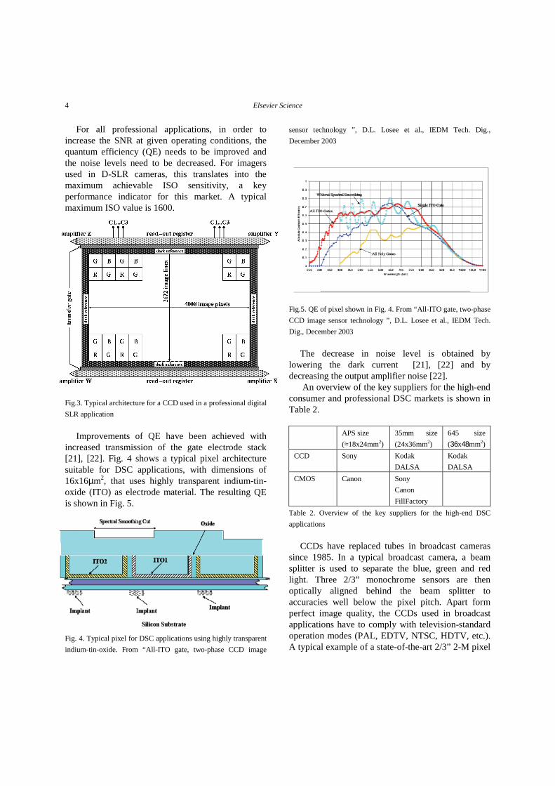
Improvements of QE have been achieved with increased transmission of the gate electrode stack [21], [22]. Fig. 4 shows a typical pixel architecture suitable for DSC applications, with dimensions of 16x16µm2, that uses highly transparent indium-tin-oxide (ITO) as electrode material. The resulting QE is shown in Fig. 5.
Fig. 4. Typical pixel for DSC applications using highly transparent
indium-tin-oxide. From “All-ITO gate, two-phase CCD image
sensor technology ”, D.L. Losee et al., IEDM Tech. Dig.,
December 2003
Fig.5. QE of pixel shown in Fig. 4. From “All-ITO gate, two-phase
CCD image sensor technology ”, D.L. Losee et al., IEDM Tech.
Dig., December 2003
The decrease in noise level is obtained by lowering the dark current [21], [22] and by decreasing the output amplifier noise [22].
An overview of the key suppliers for the high-end consumer and professional DSC markets is shown in Table 2.
APS size
(≈18x24mm2)
35mm size
(24x36mm2)
645 size
(36x48mm2)
CCD Sony Kodak
DALSA
Kodak
DALSA
CMOS Canon Sony
Canon
FillFactory
Table 2. Overview of the key suppliers for the high-end DSC
applications
CCDs have replaced tubes in broadcast cameras since 1985. In a typical broadcast camera, a beam splitter is used to separate the blue, green and red light. Three 2/3” monochrome sensors are then optically aligned behind the beam splitter to accuracies well below the pixel pitch. Apart form perfect image quality, the CCDs used in broadcast applications have to comply with television-standard operation modes (PAL, EDTV, NTSC, HDTV, etc.). A typical example of a state-of-the-art 2/3” 2-M pixel

Elsevier Science 5
FT-CCD sensor with switchable aspect ratio is shown in Fig. 6 [23]. The use of a 12-phase image structure allows switchability between 4:3 and 16:9 aspect ratio with a constant horizontal field-of-view.
The major challenge for applying CCDs to cinematographic applications is to combine perfect image quality with very high resolution and high frame rates. An 8M-pixel FT-CCD with on-chip RGB color filters and 16 parallel outputs has been presented that complies with the demands for a digital cinema camera [24], fig 7. The sensor, with 8.4x8.4µm2 pixels, achieves 12 bit DR and is compatible with existing optical systems. The minimum requirement of 24 frames per second is achieved with a reset frequency of the amplifiers of 20MHz. The maximum frame rate is 60 fps.
Fig. 6. Example of a 2/3” 2-M pixel FT-CCD for broadcast
applications. From “CCD Imagers for broadcast applications”. H.
Stoldt et al., IEDM Tech. Dig., pp. 899 - 902, December 1996
For static medical X-ray imaging, high-resolution (>16M pixels) FF-CCD imagers with very large imaging arrays are required, typically 5x5cm2. For dynamic medical X-ray imaging, at least 15 fps, but
preferably 30 fps are required with a resolution of >1M pixels and with image diagonals between ½” and 1”. Most applications use FT-CCDs. For more details, see the overview paper [25] in this issue.
Fig. 7. 8M-pixel FT-CCD for digital cinema applications. From
“Ultra-high resolution image capturing and processing for digital
cinematography”, A. Theuwissen et al., ISSCC Tech. Digest,
2003.
4. CCD imagers for industrial applications
Some of the of industrial applications can be covered by area sensors that are very similar to those used in medical or consumer DSC applications.
However, for specific industrial and most of the scientific applications, the sensor requirements differ too much from mainstream CCD developments. Specific CCDs need to be designed and dedicated technologies need to be developed.
4.1. Line scan sensors
For industrial inspection, often line scan sensors are used e.g. for inspection of moving objects on a conveyor belt. The sensor is scanning in one dimension and the mechanical movement results in scanning in the perpendicular direction.
The state-of-the art line scan sensors can have up to 12000 pixels on a 5µm pitch, with up to 320 MHz data rate [26]. Whereas in the past, monochrome

Elsevier Science6
applications dominated this market, color line scan sensors are becoming more widely used.
4.2. TDI image sensors
A TDI CCD (time-delay and integrate) can be considered a full-frame CCD sensor that is continuously being read out [1]. By synchronizing the vertical transport speed of the array with the movement of the object that is being imaged, the sensitivity can be increased by a factor N (from 1 for a line sensor to N, the number of lines, in a TDI sensor) without any degradation of resolution. Since the increase in sensitivity is relying on the summation of charge packets in the charge domain, this is a noise-free operation [1]. Most TDI imagers have a very wide aspect ratio, e.g. 100:1. Both for line scan and TDI sensors, increasing the data rate is a major challenge, that needs to be addressed by higher-speed output amplifiers (e.g. from 25MHz to 40MHz) or more taps (e.g. for every 512 columns in stead of for every 1024 columns). Current state-of-the art are TDI imagers with 8192 columns and 96 rows, a pixel size of 7x7µm2 and with up to 640MHz data rate by the use of 16 parallel outputs [27].
4.3. Area image sensors
In industrial applications, low-smear requirements make IL-CCDs often the preferred choice. In other industrial applications where smear [1] is less important, but high pixel aperture and wide DR are appreciated, FF- and FT-CCDs are often used.
5. CCD imagers for scientific applications
Specially developed area image sensors for scientific applications are mainly used when the requirements of focal plane size, resolution, pixel size, spectral range, dark current, dynamic range, speed and radiation-hardness differ too much from mainstream CCD developments [28].
5.1. Size and resolution
The largest CCDs cover an entire 6” CCD wafer. CCDs with 7168x8192 pixels of 12x12 µm2 size [29] and 9216 x 9216 pixels of 8.75x8.75µm2 size have been reported [28],[30]. Special design techniques are needed to achieve sufficient yield and to obtain the required extremely high transport efficiency. A typical example of a FT-CCD design adapted to the 4” wafer size is shown in fig. 8 [31]. To assemble even large-size focal plane arrays, three-side buttable CCD imagers have been presented [32].
Fig. 8. FT-CCD design adapted to the wafer size. From “Large
format backside illuminated CCD imager for space surveillance ”,
John R. Tower et al., IEEE T-ED, vol. 50, January 2003.
5.2. Spectral range
Fig. 9 shows the absorption length of photons in silicon.
The spectral range in silicon-based imagers is limited at long wavelengths to about 1100nm, when the energy of the photons becomes smaller than the bandgap (1.1eV in silicon) . For wavelengths shorter than 400nm (>3.1eV in silicon) more than one electron-hole pair is generated per incident photon. [28].
The very short absorption depths for UV photons (10 to 100 nm in silicon) seriously limits the QE of

Elsevier Science 7
front-side illuminated CCDs for the detection of wavelengths between 120nm and 400nm. Initial results of CCD detection of 157nm photons on frontside-illuminated CCD line scan sensor have been reported [33], where most of the stack was etched away above the photodiode to limit the absorption.
Fig. 9. Absorption length of photons in silicon. From “Deep-
depletion CCDs with improved UV sensitivity”, Jan T. Bosiers et
al., IEDM Tech. Dig., December 1985
Non-silicon based CCD imagers have been developed to image in the infrared spectral range. Monolithic InSb CCD imagers were reported as early as 1978 [34] for operation from 2.0µm to 5.5µm wavelengths. A monolithic InSb wafer-scale FF-CCD with 25x25µm2 pixels and 2Kx2K resolution was presented recently [35].
The composition of HgCdTe can be tuned for use in wavelength ranges from 1.0µm to 2.5µm, from 3.0µm to 5.0µm and from 8.0µm to 12µm. [36]. A wafer-scale monolithic HgCdTe CCD imager with 2Kx2K resolution and 20x20µm2 pixels was presented for operation in the 1.0 to 2.5µm wavelength range [37].
Another approach for IR-detection is to attach detector arrays made in e.g. InSb or MgCdTe to a mono-silicon area-CCD readout circuit.
5.3. High Resistivity and Deep Depletion
Since the absorption lengths in silicon are quite long for infra-red light (700nm-1100nm) and for a wide range of X-ray irradiation, this can degrade both the sensitivity and MTF [38]. By building imagers on high-resistivity substrates, the depletion depths can be increased from typically 4-10µm to 100-300 µm [28]. [39], [40], [41], [42]. This extends the usable X-ray range to 15keV and significantly improves the QE for the near infrared (700-1100nm).
5.4. Backside Illumination
Backside illumination to improve the quantum efficiency for CCDs for visible light applications was first presented in 1973 [43]. The approach is still occasionally used for CCDs for visible-light imaging, e.g. in space applications where a lateral overflow drain structure can be incorporated to avoid image degradation by overexposure [31], (Fig.10). An excellent QE can be achieved over a wide wavelength range, as shown in Fig.11.
Fig.10. Backside thinned CCD with lateral overflow drain
structure. From “Large format backside illuminated CCD imager
for space surveillance”, John R. Tower et al., IEEE T-ED, vol. 50,
January 2003
To overcome the problems arising from the very short absorption depths for UV photons (10 to

Elsevier Science8
100nm), backside illumination is often preferred for imaging at these wavelengths. Thus the absorption of UV photons in the front-side layer stack needed to build the CCD structure can be avoided [44], [45]. The drive for lower-wavelength sensitivity comes from space applications but also from the semiconductor inspection equipment, where ever smaller particles need to be detected.
Fig.11. Typical QE for back-illuminated backside-thinned CCDs.
From “Large format backside illuminated CCD imager for space
surveillance”, John R. Tower et al., IEEE T-ED, vol. 50, January
2003
Two approaches are currently used to manufacture devices with high QE in the 120nm-400nm range: backside thinning and high-resistivity substrates. In backside thinned devices [46], the wafers or individual CCDs are thinned to about 10mm. The advantage of using thinned devices is that standard CCD wafers and process technology can be used. However, once the wafer or the individual devices has been thinned, only a small range of process options can still be used.
The advantage of using high-resistivity wafers is that more process options are available after thinning. However, special care needs to be taken to ensure that the high resistivity is not degraded during processing [45]. Fig. 12 shows a typical backside illuminated CCD. The QE obtained on this device is shown in fig.13.
In all backside illuminated CCDs, a special backside treatment is required to control the dark
current and to obtain sufficient operating stability [28],[46],[47].
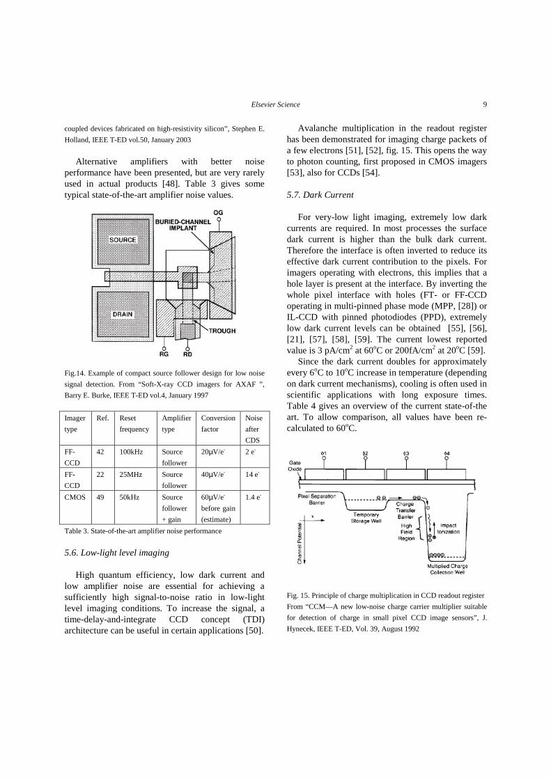
5.5. Low-noise readout
A very low amplifier noise floor of only a few electrons can be achieved at low pixel frequencies (100kHz or less) with a compact design of the source-follower amplifier. Noise levels as low as 2 electrons at 100kHz have been reported for a traditional source-follower combined with correlated double sampling noise reduction, fig. 14 [42].
Fig.12. Example of back-illuminated CCD on high-resistivity
silicon. From ““Fully depleted, back-illuminated charge-coupled
devices fabricated on high-resistivity silicon”, Stephen E. Holland,
IEEE T-ED vol.50, January 2003
Fig.13. Typical QE curve for back-illuminated CCD built on high-
resistivity silicon. From “Fully depleted, back-illuminated charge-
Elsevier Science 9
coupled devices fabricated on high-resistivity silicon”, Stephen E.
Holland, IEEE T-ED vol.50, January 2003
Alternative amplifiers with better noise performance have been presented, but are very rarely used in actual products [48]. Table 3 gives some typical state-of-the-art amplifier noise values.
Fig.14. Example of compact source follower design for low noise
signal detection. From “Soft-X-ray CCD imagers for AXAF ”,
Barry E. Burke, IEEE T-ED vol.4, January 1997
Imager
type
Ref. Reset
frequency
Amplifier
type
Conversion
factor
Noise
after
CDS
FF-
CCD
42 100kHz Source
follower
20µV/e- 2 e-
FF-
CCD
22 25MHz Source
follower
40µV/e- 14 e-
CMOS 49 50kHz Source
follower
+ gain
60µV/e-
before gain
(estimate)
1.4 e-
Table 3. State-of-the-art amplifier noise performance
5.6. Low-light level imaging
High quantum efficiency, low dark current and low amplifier noise are essential for achieving a sufficiently high signal-to-noise ratio in low-light level imaging conditions. To increase the signal, a time-delay-and-integrate CCD concept (TDI) architecture can be useful in certain applications [50].
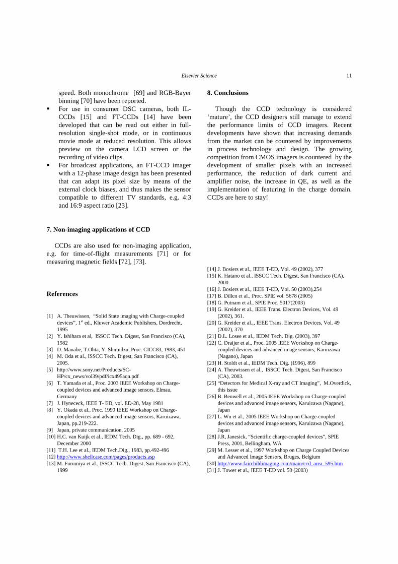
Avalanche multiplication in the readout register has been demonstrated for imaging charge packets of a few electrons [51], [52], fig. 15. This opens the way to photon counting, first proposed in CMOS imagers [53], also for CCDs [54].
5.7. Dark Current
For very-low light imaging, extremely low dark currents are required. In most processes the surface dark current is higher than the bulk dark current. Therefore the interface is often inverted to reduce its effective dark current contribution to the pixels. For imagers operating with electrons, this implies that a hole layer is present at the interface. By inverting the whole pixel interface with holes (FT- or FF-CCD operating in multi-pinned phase mode (MPP, [28]) or IL-CCD with pinned photodiodes (PPD), extremely low dark current levels can be obtained [55], [56], [21], [57], [58], [59]. The current lowest reported value is 3 pA/cm2 at 60oC or 200fA/cm2 at 20oC [59].
Since the dark current doubles for approximately every 6oC to 10oC increase in temperature (depending on dark current mechanisms), cooling is often used in scientific applications with long exposure times. Table 4 gives an overview of the current state-of-the art. To allow comparison, all values have been re-calculated to 60oC.
Fig. 15. Principle of charge multiplication in CCD readout register
From “CCM—A new low-noise charge carrier multiplier suitable
for detection of charge in small pixel CCD image sensors”, J.
Hynecek, IEEE T-ED, Vol. 39, August 1992

Elsevier Science10
5.8. Dynamic range
Large pixel sizes and low-noise readout allow dynamic ranges of up to 100dB [28]. For use in DSC applications, an IL-CCD has been presented in which every pixel comprises one large and one small photodiode enabling a four times higher dynamic range at the expense of more complicated image processing [60].
Ref
.
Reported
dark
current
[pA/cm2]
Reported
Temp.
[oC]
Device type Estimated
dark current
at 60oC
[pA/cm2]
28 40 35 FF-CCD
with MPP
320
22 100 60 FF-CCD w/o
MPP
100
21 41 55 FF-CCD
with MPP
60
57 60 60 CMOS with
PPD
60
58 6 60 IL-CCD,
PPD only,
excluding
readout
6
59 3 60 FF-CCD
with MPP
3
Table 4. Overview of dark current performance figures
5.9. High-speed image readout
Most CCDs use a (single or multiple) source-follower type amplifier. This generally limits the pixel frequency to 25-40MHz, with an amplifier bandwidth in the range of 75MHz to 120MHz. A CCD with a triple source follower operating at 118MHz pixel frequency with more than 250MHz bandwidth for use in broadcast applications has been presented [61].
Multiple outputs are often used to increase the pixel rate: two output amplifiers are common in FT-CCDs [62], four outputs are used in FF-CCDs [14], and up to 16 outputs in TDI imagers [27].
5.10. High-speed image capture
The concept of a high-speed image capture CCD in which each photo site is provided with a number of storage cells, was first presented in 1997 [63]. Currently, imagers have shown image capture rates of up to 1M fps, for up to 140 consecutive images, with a resolution of 300k pixels [64], [65]. To overcome the problem of the reduction in fill factor, a back-side illuminated concept has been proposed that should yield 100% fill factor [66].
5.11. Radiation hardness
Radiation effects can divided in [67]:� Transient charge production � Ionization damage. The trapping of charge in the
gate dielectric, which is dependent on the electric field, creates potential shifts and can lead to generation of interface states.
� Bulk displacement damage will generate higher bulk dark current and degradation in transport efficiency.
Radiation hardening is often needed for space applications and medical or scientific X-ray imaging. This can be achieved both by adapted designs and by optimized process technologies. See [68] in this issue for an overview.
6. Featuring in CCD imagers
Several ‘features’ can be implemented in CCD imagers. � By adapting the clock pulses in FF-CCDs the
user can often chose between read out through one, two or four amplifiers. This offers a trade-off between speed and system complexity [14], [19].
� Another specific advantage of CCD imagers is ‘binning’: the charge of e.g. 2x2 neighboring pixels is added before readout. This allows increasing the sensitivity by a factor of four without increasing noise, since the operation is performed in the charge domain. Thus it is possible to exchange resolution for SNR in low-light conditions, or to exchange resolution for
Elsevier Science 11
speed. Both monochrome [69] and RGB-Bayer binning [70] have been reported.
� For use in consumer DSC cameras, both IL-CCDs [15] and FT-CCDs [14] have been developed that can be read out either in full-resolution single-shot mode, or in continuous movie mode at reduced resolution. This allows preview on the camera LCD screen or the recording of video clips.
� For broadcast applications, an FT-CCD imager with a 12-phase image design has been presented that can adapt its pixel size by means of the external clock biases, and thus makes the sensor compatible to different TV standards, e.g. 4:3 and 16:9 aspect ratio [23].
7. Non-imaging applications of CCD
CCDs are also used for non-imaging application, e.g. for time-of-flight measurements [71] or for measuring magnetic fields [72], [73].
8. Conclusions
Though the CCD technology is considered ‘mature’, the CCD designers still manage to extend the performance limits of CCD imagers. Recent developments have shown that increasing demands from the market can be countered by improvements in process technology and design. The growing competition from CMOS imagers is countered by the development of smaller pixels with an increased performance, the reduction of dark current and amplifier noise, the increase in QE, as well as the implementation of featuring in the charge domain. CCDs are here to stay!
References
[1] A. Theuwissen, “Solid State imaging with Charge-coupled devices”, 1st ed., Kluwer Academic Publishers, Dordrecht, 1995
[2] Y. Ishihara et al, ISSCC Tech. Digest, San Francisco (CA), 1982
[3] D. Manabe, T.Ohta, Y. Shimidzu, Proc. CICC83, 1983, 451[4] M. Oda et al., ISSCC Tech. Digest, San Francisco (CA),
2005. [5] http://www.sony.net/Products/SC-
HP/cx_news/vol39/pdf/icx495aqn.pdf[6] T. Yamada et al., Proc. 2003 IEEE Workshop on Charge-
coupled devices and advanced image sensors, Elmau, Germany
[7] J. Hynececk, IEEE T- ED, vol. ED-28, May 1981[8] Y. Okada et al., Proc. 1999 IEEE Workshop on Charge-
coupled devices and advanced image sensors, Karuizawa, Japan, pp.219-222.
[9] Japan, private communication, 2005[10] H.C. van Kuijk et al., IEDM Tech. Dig., pp. 689 - 692,
December 2000[11] T.H. Lee et al., IEDM Tech.Dig., 1983, pp.492-496[12] http://www.shellcase.com/pages/products.asp[13] M. Furumiya et al., ISSCC Tech. Digest, San Francisco (CA),
1999
[14] J. Bosiers et al., IEEE T-ED, Vol. 49 (2002), 377[15] K. Hatano et al., ISSCC Tech. Digest, San Francisco (CA),
2000.[16] J. Bosiers et al., IEEE T-ED, Vol. 50 (2003),254 [17] B. Dillen et al., Proc. SPIE vol. 5678 (2005) [18] G. Putnam et al., SPIE Proc. 5017(2003)[19] G. Kreider et al., IEEE Trans. Electron Devices, Vol. 49
(2002), 361.[20] G. Kreider et al.,, IEEE Trans. Electron Devices, Vol. 49
(2002), 370[21] D.L. Losee et al., IEDM Tech. Dig. (2003), 397[22] C. Draijer et al., Proc. 2005 IEEE Workshop on Charge-
coupled devices and advanced image sensors, Karuizawa (Nagano), Japan
[23] H. Stoldt et al., IEDM Tech. Dig. )1996), 899[24] A. Theuwissen et al., ISSCC Tech. Digest, San Francisco
(CA), 2003. [25] “Detectors for Medical X-ray and CT Imaging”, M.Overdick,
this issue[26] B. Benwell et al., 2005 IEEE Workshop on Charge-coupled
devices and advanced image sensors, Karuizawa (Nagano), Japan
[27] L. Wu et al., 2005 IEEE Workshop on Charge-coupled devices and advanced image sensors, Karuizawa (Nagano), Japan
[28] J.R, Janesick, “Scientific charge-coupled devices”, SPIE Press, 2001, Bellingham, WA
[29] M. Lesser et al., 1997 Workshop on Charge Coupled Devices and Advanced Image Sensors, Bruges, Belgium
[30] http://www.fairchildimaging.com/main/ccd_area_595.htm[31] J. Tower et al., IEEE T-ED vol. 50 (2003)

Elsevier Science12
[32] B. Burke et al., IEEE T-ED vol. 38 (1991)[33] F. Li et al., Proc 2003 IEEE Workshop on Charge-coupled
devices and advanced image sensors, Elmau, Germany[34] R.D. Thom et al., IEDM Tech. Dig., pp. 501 - 504, December
1978.[35] A. Hoffman et al. Proc. SPIE, vol. 5499, 2004[36] D.D. Buss et al., IEDM Tech. Dig. (1978) 496[37] P. Love et al., Proc. SPIE, vol. 5499 (2004)[38] W.F. Kosonocky, IEDM Tech. Dig.(1983)[39] M.C Peckerar et al., IEEE T-ED (1979)[40] J. Janesick et al., Proc. SPIE 570 (1985).[41] J.T. Bosiers et al., IEDM Tech. Dig. (1985)[42] B.Burke et al., IEEE T-ED. (1997)[43] S.R. Shortes et al., IEDM Tech. Digest (1973), 415[44] B. E. Burke, 1997 IEEE Workshop on Charge-coupled
devices and advanced image sensors, Bruges, Belgium,[45] S. Holland et al., IEEE T-ED (2003)[46] M. Lesser, Proc. SPIE, vol. 5499 (2004).[47] M. Muramatsu et al., Proc SPIE vol. 3019. 1997[48] E. Roks, P.. Centen, J. Bosiers, W. Huinink, IEEE T-ED, vol.
43 (1996), 1583[49] A. Krymski, N. Khaliullin and H. Rhodes, Proc. 2003 IEEE
Workshop on Charge-coupled devices and advanced image sensors, Elmau, Germany
[50] M Farrier and R. Dyck, IEEE_T-ED, vol 27 (1980)[51] J. Hynecek, IEEE T-ED, vol. 39 (1992)[52] P. Jerram et al., Proc. SPIE, vol. 4306 (2001)[53] M.Campbell et al, Proc. 2003 IEEE Workshop on Charge-
coupled devices and advanced image sensors, Elmau, Germany
[54] J. Hynecek, IEEE T-ED, vol. 48 (2001)[55] N.S. Saks, IEEE ED-L, vol EDL-1 (1980)
[56] J. Bosiers et al, IEDM Tech. Dig. (1992), 97[57] S. Inoue et al., Proc. 2001 IEEE Workshop on Charge-
coupled devices and advanced image sensors, Lake Tahoe, USA, 16.
[58] C. Parks and D.S. Losee, Proc. SPIE vol. 5017 (2003), 167[59] I.M. Peters et al., Proc. 2005 IEEE Workshop on Charge-
coupled devices and advanced image sensors, Karuizawa (Nagano), Japan
[60] N. Kubo et al., Proc. SPIE vol. 5301 (2004)[61] T. Honda et al., Proc. 2005 IEEE Workshop on Charge-
coupled devices and advanced image sensors, Karuizawa (Nagano), Japan
[62] A. Stravers et al., Proc. SPIE vol. 5677 (2005)[63] F.W. Kosonocky et al., IEEE T-ED vol. 44 (1997)[64] T.G. Etoh et al., IEEE T-ED vol. 50 (2003) [65] K. Reich et al., IEEE T-ED, vol. 48 (2001)[66] T.G. Etoh ety al., Proc. 2005 IEEE Workshop on Charge-
coupled devices and advanced image sensors,, Karuizawa, Japan, pp.113-116.
[67] R.R. Hopkinson, Radiat. Phys. Chem. Vol. 43 (1994)[68] “Radiation Tolerant Sensors for Pixel Detectors”, M. Moll,
this issue[69] G.R. Sims, SPSE’s Conference & Exhibition on Electronic
Imaging, October 1986, Arlington, VA[70] C. Draijer et al., IEDM Tech.Dig. 2005, to be published[71] R. Lange and P. Seitz, IEEE Journal of Quantum Electronics,
vol. 37 no. 3 (2003), 390[72] A. Honda and K. Shirae, IEEE Transactions on Magnetics,
1981[73] N. O. and A. Nathan, IEDM Tech. Dig. (1995), 167.