Embed Size (px)
Citation preview

This document may contain technologies regulated by law [ECCN: 5E001.c.1, 5E001.c.2.d, 5E991 as of April 2005]. In the case of the export of product(s) and/or technologies described in this document, please take the appropriate procedure in conforming to all regulations related to the export.
Technical Data (Rev. 0.2, Mar. 2nd 2009) TRF2001FN-GA000-x
XFP 850 nm wavelength 10Gbit/s serial Transceiver All specifications described herein are subject to change without prior notice
10GBASE-S in 10Gigabit Ethernet [1] & 1200-MX-SN-I in 10Gigabit Fiber Channel [2] Dual Protocol Transceiver with or without FEC
Sample Categories and Disclaimer
Functional sample that has the suffix of “-F” or “-Fx” to the product number is a sample that is designed according to the customer’s request. The purpose of this sample is to check and confirm the product feasibility. Thus the sample may be an R&D prototype or may be a modified current product. This sample may not be manufactured in qualified production lines nor using qualified parts. Basically Opnext guarantees the requested performance of BOL (Beginning Of Life). Any qualification will not be applied.
Working sample that has the suffix of “-W” or “-Wx” to the product number is a sample to evaluate, confirm and finalize the product specifications. Basically Opnext guarantees the performance of BOL (Beginning Of Life). Not all qualifications may be completed. This sample may not be manufactured in qualified production lines nor be using qualified components. Until Opnext Inc. releases the products for general sales, Opnext Inc. reserves the right to change prices, features, functions, specifications, capabilities and release schedule.
FEATURES
· 10Gigabit Ethernet (10GbE) and 10Gigabit Fiber Channel (10GFC) Dual Protocol Transceiver
· 9.95328Gbit/s, 10.3125Gbit/s (10GbE) , 10.51875Gbit/s (10GFC), 11.09 Gbit/s (10GbE over G.709) and 11.318 Gbit/s (10GFC over G.709) Multi Rate Capability
· 10Gbit/s Electrical Serial Interface (XFI): 9.95, 10.31, 10.51, 11.09 and 11.32 Gbit/s · Up to 300m reach over 50/125 µm MMF with Minimum modal bandwidth @850 nm of
2,000 MHz•km [1][2]
· Compliant to IEEE 802.3ae 10GBASE-S and 10GFC 1200-MX-SN-I Application [1][2]
· Compliant to XFP MSA [3]
· 850 nm wavelength VCSEL for Optical light source
· PIN Photo detector for Optical receiver
· Low power consumption: 1.5 W maximum
· Operating Case Temperature: -5 to 70 deg C
· Compact size (18.35 x 78.0 x 8.5 mm3)
· LC-Duplex Optical Receptacle
· Hot Z-Pluggable to 30-pin electrical connector
· Latching mechanism: Lever Latch
· I2C Interface for Management Signal [4]
· XFI Loopback function available

Confidential: Technical Data of TRF2001FN-GA000-x (Rev. 0.2/March 2nd 2009) Opnext
- 2 -
REFERENCE
[1] IEEE 802.3ae D5.0 as 10GBASE-L [2] ANSI 10 Gigabit Fiber Channel, Rev 3.2 [3] XFP MSA, Rev.4.5 [4] Opnext TRF20xx/50xx/70xx I2C Specifications OPN-DST-04026-1.4 (Mar. 12th, 2007)

Confidential: Technical Data of TRF2001FN-GA000-x (Rev. 0.2/March 2nd 2009) Opnext
- 3 -
DESCRIPTION
Opnext’s 10 Gbit/s serial transceiver module TRF2001FN-GA000-x enables a dense-port and high-throughput solution in favor of its compact size and low power consumption. The TRF2001FN-GA000-x modules can be used in Datacom applications, such as 10Gigabit Ethernet (10GbE) and 10Gigbit Fiber Channel (10G FC). The maximum transmission length of TRF2001FN-GA000-x is x is defined from 26m to 300m, depending on multimode fiber types [1][2]. TRF2001FN-GA000-x is a fully integrated 10Gbit/s serial optical transceiver module that consists of a 850 nm wavelength VCSEL, Driver IC, PIN photo-diode, pre-amplifier, Transceiver IC including signal conditioner of electrical interface with post-amplifier. The 10Gbit/s electrical serial interface (XFI) to ASIC/SerDes circuit in Customer’s board is compliant with 10Gbits Small Form Factor Pluggable Module Multi–Source Agreement (XFP MSA) [3]. Mechanical dimensions, connecters and footprint of TRF2001FN-GA000-x conform to XFP MSA. The module size is 18.35 mm x 78.0 mm x 8.5 mm and hot pluggable in Z-direction by 30-pin connector. The maximum power consumption is 1.5 W and power supply voltage is +3.3 V.
Example of XFP module application
TRF2001FN-GA000-x
Heat Sink (option)
Cage Assembly
Host Board
Clip (option)
Confidential: Technical Data of TRF2001FN-GA000-x (Rev. 0.2/March 2nd 2009) Opnext
- 4 -
Block Diagram
LD Driver LD
Pre- amplifier
Optical Output
GND
TD+/-
RefCLK+/-
Rx_LOS
Mod_NR
Pin-PD Signal
Conditioner
Signal
Conditioner
RD+/-
Optical Input
VCC3
SDA
VCC5
VCC2
TX_DIS
Interrupt
2-wire interface Control
Mod_ABS
Mod_DeSel
SCL
P_Down/RST
Control/ Status
Figure 1 Schematic block diagram of the transceiver module

Confidential: Technical Data of TRF2001FN-GA000-x (Rev. 0.2/March 2nd 2009) Opnext
- 5 -
Functional Description
Data and Clock
(1) Transmitter Data Interface (XFI interface at point B’ in Figure 2) No. Symbol Function I/O Logic Remarks 1 TD +/- Transmitter Data Input I CML
(2) Receiver Data Interface (XFI interface at point C’ in Figure 2)
No. Symbol Function I/O Logic Remarks 1 RD +/- Receiver Data Output O CML
50
Connector
50
ASIC/SerDes Transceiver
50
50
50
50
50
50
C C’ D
A B’ B
Host Board
Figure 2 Interface to ASIC/SerDer
The Transceiver module’s XFI Electrical interface are specified at the Point C’ and B’, shown as Table 7, 8, 9 and10.
(3) Reference Clock (Note 1)
No. Symbol Function I/O Logic Remarks 1 Ref CLK +/- Reference Clock I LVPECL AC coupled
Note 1: Reference clock is not used in this product. But maybe used in future products. It is highly recommended to have the reference clock available on the host board.
Transceiver Module
REFCLK
Z= 50
Z= 50
VDD
VBB
50 or Z= 100 balanced
Ref_CLK
Figure 3 Interface of Reference Clock

Confidential: Technical Data of TRF2001FN-GA000-x (Rev. 0.2/March 2nd 2009) Opnext
- 6 -
Control
(1) TX_DIS No. TX_DIS Function Logic Termination 1 H Transmitter laser source
Turn off 2 L Normal
LV-TTLPulled up to VCC3 by(>=10k ohm) resistor
(2) P_DOWN/RST No. P_Down/RST Function Logic Termination
Transceiver Reset (Negative edge of this signal)
1 H
Standby (Low Power) mode with a maximum power dissipation of 1.5 W
2 L Normal
LV-TTLPulled up to VCC3 by(>=10k ohm) resistor
Status
(1) Mod_NR No. Mod_NR Function Logic Termination 1 H Module Operational Fault 2 L Normal
LV-TTL Open collector
(2) Interrupt
No. Interrupt Function Logic Termination 1 H Normal 2 L Possible module Operational fault or
a status critical to the Host SystemLV-TTL Open collector
(3) Mod_ABS Mod_ABS is pulled up to VCC3 on the Host board and grounded in the transceiver module. This pin is then asserted “H” when the Transceiver module is physically absent from a host slot. (4) RX_LOS
No. RX_LOS Function Logic Termination 1 H Insufficient optical power 2 L Normal
LV-TTL Open corrector
2-Wire Interface
(1) SDA and SCA (Note 1) No. Symbol Function I/O Logic Remark 1 SDA 2-Wire Serial Interface Data Line I/O LV-TTL I2C Compatible2 SCL 2-Wire Serial Interface Clock I LV-TTL I2C Compatible
Note1: Refer to Opnext TRF20xx/50xx/70xx I2C Specifications OPN-DST-04026-1.4 (Mar. 12th, 2007) [4] for I2C Management interface. See Appendix A for the serial ID memory map located in Lower Table in the lower address and Table 01h in the upper address defined in the Opnext TRF20xx/50xx/70xx I2C Specifications.

Confidential: Technical Data of TRF2001FN-GA000-x (Rev. 0.2/March 2nd 2009) Opnext
- 7 -
(2) Mod_DeSel
No. MOD_DeSel Function I/O Logic Termination 1 H 2-Wire Serial Interface is
used by other device 2 L to respond to 2-Wire Serial
Interface
I LV-TTLPulled up to VCC3 by(>=10k ohm) resistor
Voltage Supply
VCC3 V Digital
Module GND
Transceiver
FIL +3.3 V
+5V (Vcc5), +1.8V (Vcc2),
-5.2 V(VEE5) : Internally open
FIL : example
30-pin
Con-
nector
Pin 8, 9
Pin 1, 7, 15, 16, 19, 23, 26, 27, 30
0.1 uF 0.1 uF22 uF
4.7 uH
Transceiver
(Note) The module is tested with a high quality power supply connected through the filter shown in this figure.
Figure 4 Recommended power supply connection

Confidential: Technical Data of TRF2001FN-GA000-x (Rev. 0.2/March 2nd 2009) Opnext
- 8 -
PERFORMANCE SPECIFICATIONS
Absolute Maximum Ratings
Stresses in excess of the Absolute Maximum Ratings can cause permanent damage to the device.
Table 1. Absolute Maximum Ratings
No. Parameter Symbol Min. Max. Unit Remarks 1 Supply Voltage VCC3 0 +3.6 V +3.3 V 2 Storage Temperature Tstr -40 85 °C 3 Optical Receiver Input Pimax - +1 dBm Average
Operating Environment Electrical and optical characteristics below are defined under this operating environment, unless otherwise specified.
Table 2. Operating Environment
No. Parameter Symbol Min. Typ. Max. Unit Remarks 1 Supply Voltage VCC3 3.13 3.3 3.47 V 2 Supply Voltage Noise
Tolerance VNTTC
Note 1 - - mVpp
3 Case Temperature TC -5 25 70 °C
Note 1: Min. 2% noise of VCC3 at less than 1 MHz, min 3% noise at 1MHz to 10 MHz

Confidential: Technical Data of TRF2001FN-GA000-x (Rev. 0.2/March 2nd 2009) Opnext
- 9 -
Optical Characteristics Table 3.1 10GbE/10GFC Optical Characteristics (Note1)
No. Parameter Symbol Min. Typ. Max. Unit Remarks - 9.95328 - Gbit/s IEEE 802.3ae- 10.3125 - Gbit/s IEEE 802.3ae
1
Signaling speed (nominal)
fD
- 10.51875 - Gbit/s ANSI 10GFC - 11.09 - Gbit/s IEEE 807.5ae - 11.318 - Gbit/s ANSI 10GFC
2 Signal speed variation from nominal fD -100 - 100 ppm 3 Center Wavelength C 840 - 860 nm 4 Maximum RMS spectral width rms Table 3.2 nm 5 Average launch power Po -7.3 - -1.3 dBm Min. is
informative 6 Minimum Launch power in OMA OMA Table 3.2 dBm Note 2 7 Off Transmit Power Poff - - -30 dBm Average 8 Extinction Ratio Er 3 - - dB 9 RIN12 OMA RIN - - -128 dB/Hz Note 2 10 Optical Return Loss Tolerance RLtol - - 12 dB 11 Transmitter eye mask - Figure 5 IEEE 802.3ae12 Transmitter and dispersion penalty - - - 3.9 dB 13 Receiver Overload Pro -1.0 - - dBm Average 14 Receiver Sensitivity in OMA Prav - - -11.1 dBm Informative 15 Stressed Receiver
Sensitivity in OMA OMArmin - - -7.5
0.18dBm mW
Note 2
16 Receiver Reflectance RL - - -12 dB 17 Vertical eye closure penalty Veyecl 3.5 - - dB Note 3 18 Stressed eye jitter Pro 0.3 - - UIpp Note 3 19 Receiver electrical 3dB upper
cutoff frequency fr - - 12.3 GHz
Note 1: Data Rate; NRZ at 9.95328 Gbit/s (10GBASE-SW), 10.3125 Gbit/s (10GBASE-SR) and 10.51875 Gbit/s (1200-MX-SN-I), 11.09 Gbit/s (10GBASE-SR over G.709) and 11.318 Gbit/s (1200-MX-SN-I over G.709) Mark Ratio 50%, PRBS=231-1, 1x10-12 BER
Note 2: OMA=10log10[2P{(A-1)/(A+1)}], A = 10(Er/10), P = 10(Pf/10)
Note 3: Those are test conditions for measuring stressed receiver sensitivity. Those are not required receiver characteristics.

Confidential: Technical Data of TRF2001FN-GA000-x (Rev. 0.2/March 2nd 2009) Opnext
- 10 -
Table 3.2 Minimum OMA (dBm) as function of center wavelength and RMS spectral width
RMS Spectral width (nm) Center wavelength
(nm) Up to 0.05 0.05 to 0.1 0.1 to 0.15 0.15 to 0.2 0.2 to 0.25 0.25 to 0.3 0.3 to 0.35 0.35 to 0.4 0.4 to 0.45
840 to 842 -4.2 -4.2 -4.1 -4.1 -3.9 -3.8 -3.5 -3.2 -2.8
842 to 844 -4.2 -4.2 -4.2 -4.1 -3.9 -3.8 -3.6 -3.3 -2.9
844 to 846 -4.2 -4.2 -4.2 -4.1 -4.0 -3.8 -3.6 -3.3 -2.9
846 to 848 -4.3 -4.2 -4.2 -4.1 -4.0 -3.8 -3.6 -3.3 -2.9
848 to 850 -4.3 -4.2 -4.2 -4.1 -4.0 -3.8 -3.6 -3.3 -3.0
850 to 852 -4.3 -4.2 -4.2 -4.1 -4.0 -3.8 -3.6 -3.4 -3.0
852 to 854 -4.3 -4.2 -4.2 -4.1 -4.0 -3.9 -3.7 -3.4 -3.1
854 to 856 -4.3 -4.3 -4.2 -4.1 -4.0 -3.9 -3.7 -3.4 -3.1
856 to 858 -4.3 -4.3 -4.2 -4.1 -4.0 -3.9 -3.7 -3.5 -3.1
858 to 860 -4.3 -4.3 -4.2 -4.2 -4.1 -3.9 -3.7 -3.5 -3.2
Table 3.3 Operating range for each optical fiber type
Fiber type Minimum modal bandwidth @ 850 nm
(MHz•km) Operating range
(m)
50 µm MMF 2000 2 to 300
50 µm MMF 500 2 to 82 (Note 1)
62.5 µm MMF 200 2 to 33 (Note 1)
Note 1: 500MHz·km and 200MHz·km modal bandwidth fiber link is guaranteed based on DELAIRE USA - Test Link System [DE27186-00].
0.250.28
0.5
0.720.75
1
0
-0.4
1.4
0.25 0.4 0.45
Time (U.I.)
0.55 0.6 0.75 0 1
Logic “0”Level
Logic “1”Level
Figure 5 Mask of Eye Diagram
Normalized Amplitude
Confidential: Technical Data of TRF2001FN-GA000-x (Rev. 0.2/March 2nd 2009) Opnext
- 11 -
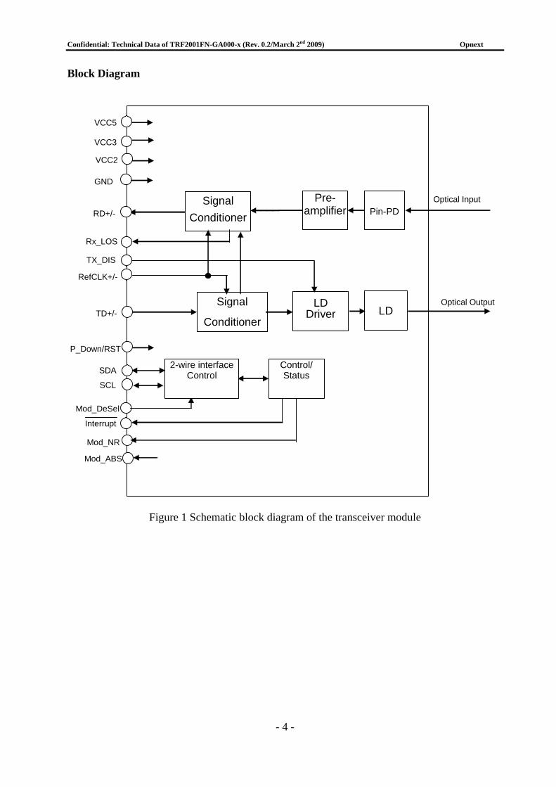
Electrical Performance
Table 4. Power supply Characteristics
No. Parameter Symbol Min. Typ. Max. Unit Remarks1 Vcc3 Supply Current Icc3 - - 0.43 A +3.3 V
Note 1
2 Vcc3 Supply Current during power down
- - - 0.43 A +3.3 V
3 Power Consumption PDS - - 1.5 W 4 Power Consumption during Power
down - - - 1.5 W
Note 1: Including in rush current. Maximum module current ramp rate is 100 mA /s.
Table 5. LVTTL level
No. Parameter Symbol Min. Typ. Max. Unit Remarks1 Input High Voltage VIH 2.0 - Vcc3+0.3 V IIH(max)=10uA
2 Input Low Voltage VIL -0.3 - 0.8 V IIL(max)=-10uA
3 Output High Voltage VOH host_Vcc-0.5
- host_Vcc+0.3
V Pulled up to host_Vcc.
4 Output Low Voltage VOL 0.0 - 0.4 V Pulled up to host_Vcc, IOL(max)=-3mA
Table6. Reference Clock Characteristics
No. Parameter Symbol Min. Typ. Max. Unit Remarks 1 Clock Differential Input
Impedance Zd 80 100 120 ohm
2 Differential Input Clock Amplitude (pp)
- 640 1600 mV AC coupled PECL
3 Reference Clock Duty Cycle - 40 60 % 4 Reference Clock Rise/Fall
Time Tr/Tf 200 1250 ps 20% to 80%
5 Reference Clock Frequency fo fD/64 MHz Note1 6 RMS Jitter Random Jitter 10 ps Up to
100MHz 7 Reference Clock Frequency
Tolerance f -100 - 100 ppm
Note1: Reference clock frequency is not locked to the data frequency and may deviate by f. fD: Nominal Bit Rate (9.95328 Gbit/s, 10.3125 Gbit/s, 10.51875 Gbit/, 11.09 Gbit/s or 11.318 Gbit/s)

Confidential: Technical Data of TRF2001FN-GA000-x (Rev. 0.2/March 2nd 2009) Opnext
- 12 -
Table 7. Transceiver Module’s XFI Transmitter Input Electrical Specification at B’
No. Parameter Symbol Min. Typ. Max. Unit Remarks 1 Differential Input Impedance Zd - 100 - ohm 2 Termination Mismatch - - - 5 %
3 Source to Sink DC Potential Difference
Vcm 0 - 3.6 V
4 Input AC Common Mode Voltage
- - - 25 mV(RMS)
20 8
- -
- -
dB dB
0.05 – 0.1GHz0.1 - 5.5GHz
5 Differential Input Return Loss SDD11
Note1 - - dB 5.5-12GHz 6 Common Mode Input Return
Loss SCC11
3 - - dB 0.1 - 15GHz
7 Differential to Common Mode Conversion
SCD11
10 - - dB 0.1 - 15GHz
Note 1 Return Loss given be equation SDD11(dB) = 8 - 20.66 log10 (f/5.5), with f in GHz.
Table 8. Transceiver Module’s XFI Transmitter Input Jitter Specification at B’
No. Parameter Symbol Min. Typ. Max. Unit Remarks 1 Total Non-DDJ Jitter - - - 0.41 UIpp 2 Total Jitter Tj - - 0.61 UIpp 3 Sinusoidal Jitter Tolerance SJ - - Note1
4 Eye Mask X1 - - 0.305 UI 5 Eye Mask Y1 60 - - mV 6 Eye Mask Y2 - - 410 mV
Note 1 Sinusoidal jitter tolerance is given by Figure 7.
Figure 6 Transceiver Module’s XFI Transmitter Differential Input compliance Mask at B’

Confidential: Technical Data of TRF2001FN-GA000-x (Rev. 0.2/March 2nd 2009) Opnext
- 13 -
Figure 7 Transceiver Module’s XFI Transmitter Input Margin Mask at B’
Table 9. Transceiver Module’s XFI Receiver Output Electrical Specification at C’
No. Parameter Symbol Min. Typ. Max. Unit Remarks 1 Differential Output
Impedance Zd - 100 - ohm
2 Termination Mismatch - - - 5 %
3 DC Common Mode Potential Vcm 0 - 3.6 V 4 Output AC Common Mode
Voltage - - - 15 mV(RM
S)
5 Output Rise and Fall time tRH,tFH 24 - - ps 20% to 80%20 8
- -
- -
dB dB
0.05-0.1GHz0.1- 5.5GHz
6 Differential output Return Loss
SDD22
Note1 - - dB 5.5-12GHz 7 Common Mode Output
Return Loss SCC22
3 - - dB 0.1 - 15GHz
Note 1 Return Loss given be equation SDD22(dB) = 8 - 20.66 log10 (f/5.5), with f in GHz.
Table10. Transceiver Module’s XFI Receiver Output Jitter Specification at C’
No. Parameter Symbol Min. Typ. Max. Unit Remarks 1 Deterministric Jitter DJ - - 0.18 UIpp 2 Total Jitter TJ - - 0.34 UIpp 3 Eye Mask X1 - - 0.17 -
4 Eye Mask X2 - - 0.42 UI 5 Eye Mask Y1 170 - - mV 6 Eye Mask Y2 - - 425 mV

Confidential: Technical Data of TRF2001FN-GA000-x (Rev. 0.2/March 2nd 2009) Opnext
- 14 -
Figure 8 Transceiver Module’s XFI Reciever Differential Output Compliance Mask at C’
Table 11. Alarm Characteristics
No. Parameter Symbol Min. Typ. Max. Unit Remarks1 Receiver Loss of Signal
Indicator Assert BER Level
Deassert BER Level
Activation Time
Deactivation Time
RX_LOS
1E-5
1E-10
2.3 -
-
-
-
100 100
-
-
s s

Confidential: Technical Data of TRF2001FN-GA000-x (Rev. 0.2/March 2nd 2009) Opnext
- 15 -
Jitter Characteristics
Table 12. Transmitter Jitter Characteristics
No. Parameter Symbol Min. Typ. Max. Unit Remarks 1 Jitter Transfer Bandwidth BW - - 8 MHz PRBS231-12 Jitter Peaking - - 1 dB freq.>50kHz
Table 13. Receiver Jitter Characteristics
No. Parameter Symbol Min. Typ. Max. Unit Remarks 1 Jitter Transfer Bandwidth BW - - 8 MHz PRBS231-12 Jitter Peaking - - 1 dB freq.>50kHz
Confidential: Technical Data of TRF2001FN-GA000-x (Rev. 0.2/March 2nd 2009) Opnext
- 16 -
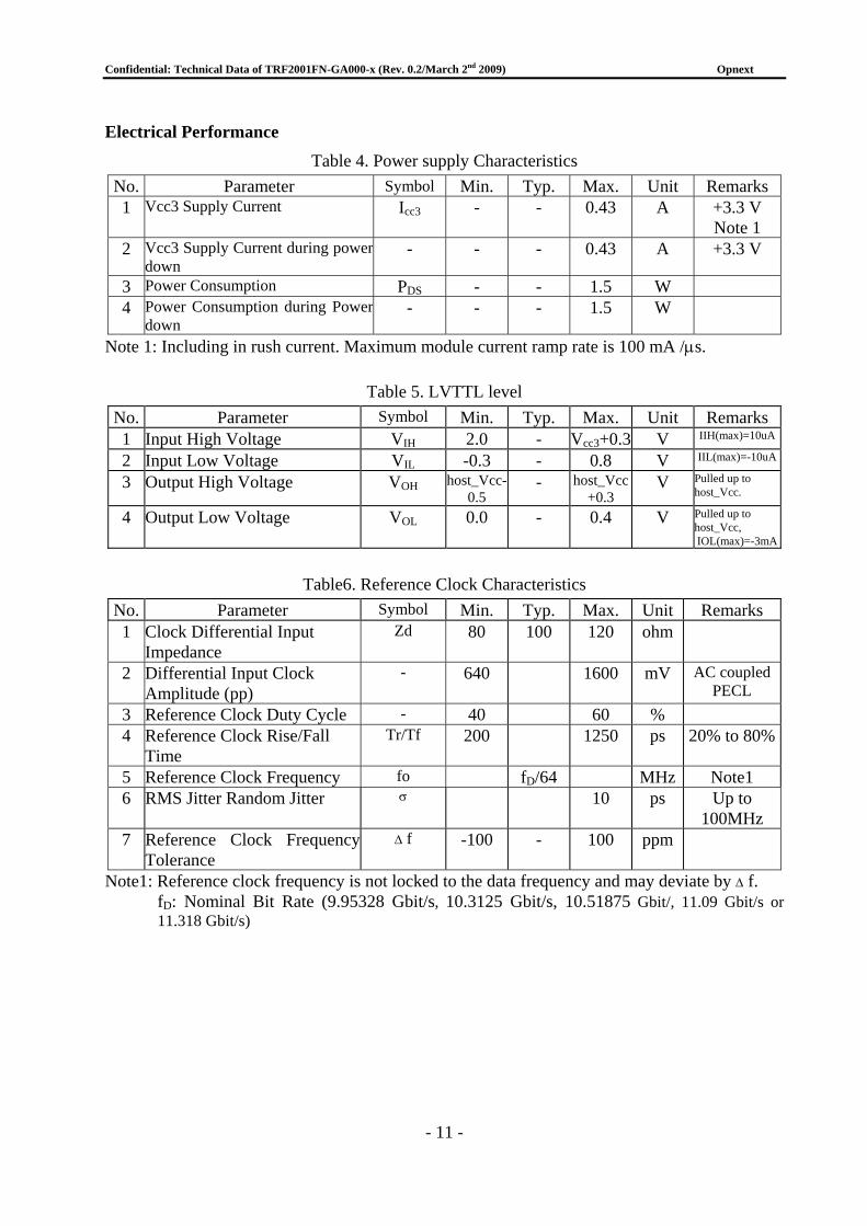
Figure 9. Pin Configuration
GND 1
GND 15
VEE5 2
MOD_DESEL 3
INT ERRUPT 4
TX_DIS 5
VCC5 6
GND 7
VCC3 8
VCC3 9
SCL 10
SDA 11
MOD_ABS 12
MOD_NR 13
RX_LOS 14
GND 30
GND 16
TD+ 29
TD- 28
GND 27
GND 26
REFCLK- 25
REFCLK+ 24
GND 23
VCC2 22
P_DOWN/RST21
VCC2 20
GND 19
RD+ 18
RD- 17
Bottom of Board (As viewed thru top of board)
Top of Board

Confidential: Technical Data of TRF2001FN-GA000-x (Rev. 0.2/March 2nd 2009) Opnext
- 17 -
Table 14. Pin Description Pin# Symbol I/O Logic Description Remarks
1 GND Supply Module Ground Note2 2 VEE5 Supply Internally open Note1 3 Mod_Desel I LVTTL Module De-select; When held low allows the module
to respond to 2-wire serial interface commands”
4 Interrupt O LVTTL Interrupt; Indicates presence of an important condition which can be read over the 2-wire serial interface
Note3
5 TX_DIS I LVTTL Transmitter Disable; Transmitter Laser Source Turned Off
6 VCC5 Supply Internally open 7 GND Supply Module Ground Note 2 8 VCC3 Supply +3.3V Power Supply 9 VCC3 Supply +3.3V Power Supply 10 SCL I/O LVTTL 2-Wire Serial Interface Clock Note3 11 SDA I/O LVTTL 2-Wire Serial Interface Data Line Note3 12 Mod_ABS O LVTTL Indicates Module is not present. Grounded in the
Module Note3
13 Mod_NR O LVTTL Module Not Ready; Indicating Module Operational Fault
Note3
14 RX_LOS O LVTTL Receiver Loss of Signal Indicator Note3 15 GND Supply Module Ground Note2 16 GND Supply Module Ground Note2 17 RD- O CML Receiver Inverted Data Output 18 RD+ O CML Receiver Non-Inverted Data Output 19 GND Supply Module Ground Note2 20 VCC2 Supply Internally open 21 P_Down/RST I LVTTL Power down; When high, requires the module to limit
power consumption to 1.5W or below. 2-Wire serial interface must be functional in the low power mode.
Reset; The falling edge initiates a complete reset of the module including the 2-wire serial interface, equivalent to a power cycle.
22 VCC2 Supply Internally open 23 GND Supply Module Ground Note2 24 RefCLK+ I PECL Reference Clock Non-Inverted Input Note 4 25 RefCLK- I PECL Reference Clock Inverted Input Note 4 26 GND Supply Module Ground Note2 27 GND Supply Module Ground Note2 28 TD- I CML Transmitter Inverted Data Input 29 TD+ I CML Transmitter Non-Inverted Data Input 30 GND Supply Module Ground Note2
Note 1. Optional – 5.2 V Power Supply in XFP MSA specification. Note 2. To isolate Module ground pin GND are isolated from module case and chassis ground within the module.(Target) Note 3. Shall be pulled up with 4.7K-10Kohms to a voltage between 3.15V and 3.45V on the host board. Note 4. AC coupled on the host board. Reference clock is not used in this product. But maybe used in future products. It is highly recommended to have the reference clock available on the host board.
Confidential: Technical Data of TRF2001FN-GA000-x (Rev. 0.2/March 2nd 2009) Opnext
- 18 -
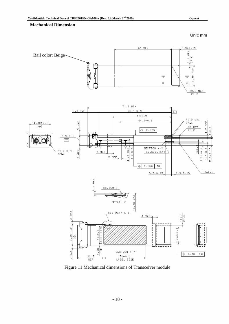
Mechanical Dimension
Unit: mm
Figure 11 Mechanical dimensions of Transceiver module
Bail color: Beige

Confidential: Technical Data of TRF2001FN-GA000-x (Rev. 0.2/March 2nd 2009) Opnext
- 19 -
Optical Interface
No. Parameter Specifications Remarks 1 Connector LC-Duplex Optical Receptacle
Electrical Connector for the customer board
No. Part name Maker Remarks 1 TYCO 788862C Or equivalent
Mechanical Parts for the customer board
No. Maker Part name Remarks 1 TYCO XFP Heat-sink Or equivalent 2 TYCO XFP Heat Sink Clip Or equivalent 3 TYCO XFP Cage Assembly Or equivalent
USER INFORMATION
Handling Precautions
CAUTION: Take proper electrostatic-discharge (ESD) precautions while handling these devices. These devices are sensitive to ESD.
EMI Compliance
This product meets Electromagnetic Interference (EMI) specifications of following standards.
No. Standards Criteria Remarks 1 FCC Class B Target 2 EN55002 Class B Target
Laser Safety
This product is complied with IEC 60825-1 as Class 1 and with FDA 21 CFR as Class I laser product. Because of size constraints, laser safety labeling is not affixed to the module but is attached to the outside of the shipping box.

Confidential: Technical Data of TRF2001FN-GA000-x (Rev. 0.2/March 2nd 2009) Opnext
- 20 -
ORDERING INFORMATION
TRF 0
1 3
x
4
w
2
x
5
x
6
x
7
x
9
x
10
x abcd
8 11
x
12
x
13
x
14
Item Parameter Symbol 1 Product Category TRF: XFP 2 Wavelength Category 3 Bit-rate Category
4
Product Code (Application/ Range)
5 Product Code
TRF2001: 850 nm wavelength VCSEL (uncooled) / PIN transceiver
6 Product Code (Function)
7 Custom/ Operating Temperature Range
FN: 10GBASE-S in 10Gigabit Ethernet and 1200-MX-SN-I in 10Gigabit Fiber Channel dual protocol transceiver with Normal operation case temperature (-5 to 70 deg C)
8 Wavelength “-”: non-WDM
9
Product Type G: General/ Standard specification (Standard includes customer designed label and ROM specifications) C: Custom specs.
10
Specification Code A: Multi Rate/ Protocol/ Product 9.95328Gbit/s, 10.3125Gbit/s (10GbE) , 10.51875Gbit/s (10GFC), 11.09 Gbit/s (10GbE over G.709) and 11.318 Gbit/s (10GFC over G.709)
11 12
Customized specification 00: Standard specification
13 Product Revision 0: Standard Full Specification
1 – 9, A-Z: custom part
14
Product Status Mn: Mechanical Sample Fn: Functional Sample (n: null or Version number) Wn: Working Sample (n: null or Version number) En: Engineering Sample Null: Mass Production

Confidential: Technical Data of TRF2001FN-GA000-x (Rev. 0.2/March 2nd 2009) Opnext
- 21 -
Document number: OPN-DST-07023-0.2 Document Category: Product Specifications (Data Sheet) Serial number OPN-DST-07023-0.2 Revision: 0.2 (March 2nd, 2009) Product Name: TRF2001FN-GA000-x
XFP 850 nm Wavelength 10 Gbits/s serial Transceiver TRF2001FN-GA000-x
Revision History
Rev. Date Page/Line/Fig/Table Modification Note 0.0 Jul. 24th, 2007 - - - 0.1 Sep. 10th,2007 All Changed the Operating Case Temperature from
0(-5 Target)℃ to -5℃. -
0.2 Mar. 2nd, 2009 Page 1 Delete “Preliminary Data Sheet Disclaimer”

Appendix A
XFP MSA Management Interface Lower Memory Map
DEC HEX Classify Name Function DescriptionVolatileor NV R or W
Volatileor NV R or W 7 6 5 4 3 2 1 0
0 00 Identifier Identifier values - R 0 0 0 0 0 1 1 0 06 61 01 Signal Conditioner Control Signale Conditioner Control Field V R/W - R 0 0 0 0 0 0
XFILoop back
0 00
2 02 Threshold Values for ALM & WRN Temp High AAlarm - R 0 1 0 1 1 0 1 0 5A 90 903 03 Threshold Values for ALM & WRN - R 0 0 0 0 0 0 0 0 0 0 deg C
4 04 Threshold Values for ALM & WRN Temp Low Alarm - R 1 1 1 1 0 1 1 0 F6 -10 -105 05 Threshold Values for ALM & WRN - R 0 0 0 0 0 0 0 0 0 0 deg C
6 06 Threshold Values for ALM & WRN Temp High Warning - R 0 1 0 1 0 1 0 1 55 85 857 07 Threshold Values for ALM & WRN - R 0 0 0 0 0 0 0 0 0 0 deg C
8 08 Threshold Values for ALM & WRN Temp Low Warning - R 1 1 1 1 1 0 1 1 FB -5 -59 09 Threshold Values for ALM & WRN - R 0 0 0 0 0 0 0 0 0 0 deg C
10 0A Threshold Values for ALM & WRN Reserved - R 0 0 0 0 0 0 0 0 0 011 0B Threshold Values for ALM & WRN - R 0 0 0 0 0 0 0 0 0 012 0C Threshold Values for ALM & WRN - R 0 0 0 0 0 0 0 0 0 013 0D Threshold Values for ALM & WRN - R 0 0 0 0 0 0 0 0 0 014 0E Threshold Values for ALM & WRN - R 0 0 0 0 0 0 0 0 0 015 0F Threshold Values for ALM & WRN - R 0 0 0 0 0 0 0 0 0 016 10 Threshold Values for ALM & WRN - R 0 0 0 0 0 0 0 0 0 017 11 Threshold Values for ALM & WRN - R 0 0 0 0 0 0 0 0 0 0
18 12 Threshold Values for ALM & WRN Bias High Alarm - R 0 0 0 1 1 0 0 1 19 6500 1319 13 Threshold Values for ALM & WRN - R 0 1 1 0 0 1 0 0 64 [0.002mA] [mA]
20 14 Threshold Values for ALM & WRN Bias Low Alarm - R 0 0 0 0 0 0 1 1 3 1000 221 15 Threshold Values for ALM & WRN - R 1 1 1 0 1 0 0 0 E8 [0.002mA] [mA]
22 16 Threshold Values for ALM & WRN Bias High Warning - R 0 0 0 1 0 1 1 1 17 6000 1223 17 Threshold Values for ALM & WRN - R 0 1 1 1 0 0 0 0 70 [0.002mA] [mA]
24 18 Threshold Values for ALM & WRN Bias Low Warning - R 0 0 0 0 0 1 0 1 5 1500 325 19 Threshold Values for ALM & WRN - R 1 1 0 1 1 1 0 0 DC [0.002mA] [mA]
26 1A Threshold Values for ALM & WRN TX Power High Alarm - R 0 0 1 0 0 0 0 0 20 8317.6 -0.827 1B Threshold Values for ALM & WRN - R 0 1 1 1 1 1 0 1 7D [0.1uW] [dBm]
28 1C Threshold Values for ALM & WRN TX Power Low Alarm - R 0 0 0 0 0 1 1 0 6 1659.6 -7.829 1D Threshold Values for ALM & WRN - R 0 1 1 1 1 0 1 1 7B [0.1uW] [dBm]
30 1E Threshold Values for ALM & WRN TX Power High Warning - R 0 0 0 1 1 1 0 0 1C 7413.1 -1.331 1F Threshold Values for ALM & WRN - R 1 1 1 1 0 1 0 1 F5 [0.1uW] [dBm]
32 20 Threshold Values for ALM & WRN TX Power Low Warning - R 0 0 0 0 0 1 1 1 7 1862.1 -7.333 21 Threshold Values for ALM & WRN - R 0 1 0 0 0 1 1 0 46 [0.1uW] [dBm]
34 22 Threshold Values for ALM & WRN RX Power High Alarm - R 0 0 1 0 0 0 1 0 22 8912.5 -0.535 23 Threshold Values for ALM & WRN - R 1 1 0 1 0 0 0 0 D0 [0.1uW] [dBm]
36 24 Threshold Values for ALM & WRN RX Power Low Alarm - R 0 0 0 0 0 0 1 1 3 912.0 -10.437 25 Threshold Values for ALM & WRN - R 1 0 0 1 0 0 0 0 90 [0.1uW] [dBm]
38 26 Threshold Values for ALM & WRN RX Power High Warning - R 0 0 0 1 1 1 1 1 1F 7943.3 -139 27 Threshold Values for ALM & WRN - R 0 0 0 0 0 1 1 1 7 [0.1uW] [dBm]
40 28 Threshold Values for ALM & WRN RX Power Low Warning - R 0 0 0 0 0 0 1 1 3 1023.3 -9.941 29 Threshold Values for ALM & WRN - R 1 1 1 1 1 1 1 1 FF [0.1uW] [dBm]
42 2A Threshold Values for ALM & WRN AUX1 High Alarm - R 1 0 0 0 1 0 0 1 89 35310.0 3.53143 2B Threshold Values for ALM & WRN - R 1 1 1 0 1 1 1 0 EE [100uV] [V]44 2C Threshold Values for ALM & WRN AUX1 Low Alarm - R 0 1 1 1 0 1 1 1 77 30690.0 3.06945 2D Threshold Values for ALM & WRN - R 1 1 1 0 0 0 1 0 E2 [100uV] [V]46 2E Threshold Values for ALM & WRN AUX1 High Warning - R 1 0 0 0 0 1 1 1 87 34650.0 3.46547 2F Threshold Values for ALM & WRN - R 0 1 0 1 1 0 1 0 5A [100uV] [V]48 30 Threshold Values for ALM & WRN AUX1 Low Warning - R 0 1 1 1 1 0 1 0 7A 31350.0 3.13549 31 Threshold Values for ALM & WRN - R 0 1 1 1 0 1 0 1 75 [100uV] [V]50 32 Threshold Values for ALM & WRN AUX2 High Alarm - R 0 0 0 0 0 0 0 0 0 051 33 Threshold Values for ALM & WRN - R 0 0 0 0 0 0 0 0 0 052 34 Threshold Values for ALM & WRN AUX2 Low Alarm - R 0 0 0 0 0 0 0 0 0 053 35 Threshold Values for ALM & WRN - R 0 0 0 0 0 0 0 0 0 054 36 Threshold Values for ALM & WRN AUX2 High Warning - R 0 0 0 0 0 0 0 0 0 055 37 Threshold Values for ALM & WRN - R 0 0 0 0 0 0 0 0 0 056 38 Threshold Values for ALM & WRN AUX2 Low Warning - R 0 0 0 0 0 0 0 0 0 057 39 Threshold Values for ALM & WRN - R 0 0 0 0 0 0 0 0 0 0
58 3A Optional VPS Control Resisters - R 0 0 0 0 0 0 0 0 0 059 3B Optional VPS Control Resisters - R 0 0 0 0 0 0 0 0 0 060 3C Reserved - R 0 0 0 0 0 0 0 0 0 061 3D Reserved - R 0 0 0 0 0 0 0 0 0 062 3E Reserved - R 0 0 0 0 0 0 0 0 0 063 3F Reserved - R 0 0 0 0 0 0 0 0 0 064 40 Reserved - R 0 0 0 0 0 0 0 0 0 065 41 Reserved - R 0 0 0 0 0 0 0 0 0 066 42 Reserved - R 0 0 0 0 0 0 0 0 0 067 43 Reserved - R 0 0 0 0 0 0 0 0 0 068 44 Reserved - R 0 0 0 0 0 0 0 0 0 069 45 Reserved - R 0 0 0 0 0 0 0 0 0 0
70 46 BER reporting - R 0 0 0 0 0 0 0 0 0 071 47 BER reporting - R 0 0 0 0 0 0 0 0 0 072 48 Wavelength Control Registers V R/MW - R 0 0 0 0 0 0 0 0 0 073 49 Wavelength Control Registers V - R 0 0 0 0 0 0 0 0 0 074 4A Wavelength Control Registers - R 0 0 0 0 0 0 0 0 0 075 4B Wavelength Control Registers - R 0 0 0 0 0 0 0 0 0 076 4C FEC Control Registers V R/MW - R 0 0 0 0 0 0 0 0 0 077 4D FEC Control Registers V - R 0 0 0 0 0 0 0 0 0 078 4E FEC Control Registers - R 0 0 0 0 0 0 0 0 0 079 4F FEC Control Registers - R 0 0 0 0 0 0 0 0 0 0
80 50 Latched InterruptB Flag FlagRead operation
-> Clear(Reset) operation - R
L-TempHighAlarm
L-TempLow
Alarm0
Reserved0
Reserved
L-TX BiasHighAlarm
L-TX BiasLow
AlarmL-TX PowerHigh Alarm
L-TXPowerLow
Alarm
81 51 Latched InterruptB Flag FlagRead operation
-> Clear(Reset) operation - R
L-RXPowerhigh
Alarm
L-RXPowe Low
Alarm
L-AUX1HighAlarm
L-AUX1Low
Alarm
L-AUX2HighAlarm
L-AUX2Low
Alarm0
Reserved0
Reserved
82 52 Latched InterruptB Flag FlagRead operation
-> Clear(Reset) operation - R
L-TempHigh
Warning
L-TempLow
Warning0
Reserved0
Reserved
L-TX BiasHigh
Warning
L-TX Bias Low
Warning
L-TX PowerHigh
Warning
L-TXPowerLow
Warning
83 53 Latched InterruptB Flag FlagRead operation
-> Clear(Reset) operation - R
L-RXPowerhigh
Warning
L-RXPowe LowWarning
L-AUX1High
Warning
L-AUX1Low
Warning
L-AUX2High
Warning
L-AUX2Low
Warning0
Reserved0
Reserved
84 54 Latched InterruptB Flag FlagRead operation
-> Clear(Reset) operation - RL-TX_NR
L-TX_Fault
L-TXCDR notLocked
L-RX_NR
L-RX_LOS
L-RXCDR notLocked
L-MOD_NR
L-ResetComplete
85 55 Latched InterruptB Flag FlagRead operation
-> Clear(Reset) operation - R
L- APDSupplyFault
L- TECFault
L- Wavelength
Unlocked0
Reserved0
Reserved0
Reserved0
Reserved0
Reserved
86 56 Latched InterruptB Flag FlagRead operation
-> Clear(Reset) operation - R
L-VCC5HighAlarm
L-VCC5Low
Alarm
L-VCC3HighAlarm
L-VCC3Low
Alarm
L-VCC2HighAlarm
L-VCC2Low
AlarmL-Vee5
High Alarm
L-Vee5Low
Alarm
87 57 Latched InterruptB Flag FlagRead operation
-> Clear(Reset) operation - R
L-VCC5High
Warning
L-VCC5Low
Warning
L-VCC3High
Warning
L-VCC3Low
Warning
L-VCC2High
Warning
L-VCC2Low
Warning
L-Vee5High
Warning
L-Vee5Low
Warning
88 58 InterruptB Masking Bits InterruptB Control V R/MW V R/MW
M-TempHighAlarm
M-TempLow
Alarm0
Reserved0
Reserved
M-TXBias High
Alarm
M-TXBias Low
Alarm
M-TXPower High
Alarm
M-TXPowerLow
Alarm
Fixed "0". Not implemented.
ADDRESS XFP MSA - Based on Rev 4.5 (August 31, 2005)
Fixed "0". Not implemented.
TRF2001FN-GA000-x
Fixed "0". Not implemented.
Bit
VPS Fields
BER Control Fields
Wavelength Control Fields
FEC Control Fields
Type Type
Fixed "0". Not implemented.
Fixed "0". Not implemented.
Fixed "0". Not implemented.
Fixed "0". Not implemented.
HEX DEC Remark
Fixed "0". Not implemented.

DEC HEX Classify Name Function DescriptionVolatileor NV R or W
Volatileor NV R or W 7 6 5 4 3 2 1 0
ADDRESS XFP MSA - Based on Rev 4.5 (August 31, 2005) TRF2001FN-GA000-x
BitType TypeHEX DEC Remark
89 59 InterruptB Masking Bits InterruptB Control V V
M-RXPowerhigh
Alarm
M-RXPowe Low
Alarm
M-AUX1HighAlarm
M-AUX1Low
Alarm
M-AUX2HighAlarm
M-AUX2Low
Alarm0
Reserved0
Reserved
90 5A InterruptB Masking Bits InterruptB Control V V
M-TempHigh
Warning
M-TempLow
Warning0
Reserved0
Reserved
M-TXBias HighWarning
M-TXBias Low
Warning
M-TXPower High
Warning
M-TXPowerLow
Warning
91 5B InterruptB Masking Bits InterruptB Control V V
M-RXPowerhigh
Warning
M-RXPowe LowWarning
M-AUX1High
Warning
M-AUX1Low
Warning
M-AUX2High
Warning
M-AUX2Low
Warning0
Reserved0
Reserved
92 5C InterruptB Masking Bits InterruptB Control V VM-TX_NR
M-TX_Fault
M-TXCDR notLocked
M-RX_NR
M-RX_LOS
M-RXCDR notLocked
M-MOD_NR
M-ResetComplete
93 5D InterruptB Masking Bits InterruptB Control V - R
M- APDSupplyFault
M- TECFault
M- Wavelength
Unlocked0
Reserved0
Reserved0
Reserved0
Reserved0
Reserved
94 5E InterruptB Masking Bits InterruptB Control - R
M-VCC5HighAlarm
M-VCC5Low
Alarm
M-VCC3HighAlarm
M-VCC3Low
Alarm
M-VCC2HighAlarm
M-VCC2Low
AlarmM-Vee5
High Alarm
M-Vee5Low
Alarm
95 5F InterruptB Masking Bits InterruptB Control - R
M-VCC5High
Warning
M-VCC5Low
Warning
M-VCC3High
Warning
M-VCC3Low
Warning
M-VCC2High
Warning
M-VCC2Low
Warning
M-Vee5High
Warning
M-Vee5Low
Warning
96 60 Temp MSB AD readout - R
97 61 Temp LSB AD readout - R
98 62 Reserved AD readout - R 0 0 0 0 0 0 0 0 0 099 63 Reserved AD readout - R 0 0 0 0 0 0 0 0 0 0
100 64 TX Bias MSB AD readout - R
101 65 TX Bias LSB AD readout - R
102 66 TX Power MSB AD readout - R
103 67 TX Power LSB AD readout - R
104 68 RX Power MSB AD readout - R
105 69 RX POwer LSB AD readout - R
106 6A AUX1 MSB AD readout - R
107 6B AUX1 LSB AD readout - R
108 6C AUX2 MSB AD readout Defined in Byte222 Page01h - R 0 0 0 0 0 0 0 0 0 0109 6D AUX2 LSB AD readout - R 0 0 0 0 0 0 0 0 0 0
110 6E General Control / Status General Control / Status Bits V R/W V R/W TXDisableState
Soft TXDisable
MON_NRSTATE
P_DownState
SoftP_Down
InterruptB RX_LOS Data_Not_Ready
111 6F General Control / Status General Control / Status Bits - R TX_NRState
TX_FaultState
TX_CDRnot
Locked
RX_NRState
RX_CDRnot
Locked0
Reserved0
Reserved0
Reserved
112 70 Reserved - R 0 0 0 0 0 0 0 0 0 0113 71 Reserved - R 0 0 0 0 0 0 0 0 0 0114 72 Reserved - R 0 0 0 0 0 0 0 0 0 0115 73 Reserved - R 0 0 0 0 0 0 0 0 0 0116 74 Reserved - R 0 0 0 0 0 0 0 0 0 0117 75 Reserved - R 0 0 0 0 0 0 0 0 0 0
118 76 Interface R/W error checking Packet Error Checking V R/W V R/W 0Reserved
0Reserved
0Reserved
0Reserved
0Reserved
0Reserved
0Reserved
PacketErrorCHK
119 77 Password Password Change Area V R/MW V R/MW
120 78 Change Password Change Area V V
121 79 Password Change Area V V
122 7A Password Change Area V V
123 7B Password Password V R/MW V R/MW
124 7C Entry Password V V
125 7D Password V V
126 7E Password V V
127 7F Page Select Page select V R/W V R/W
Note 1 The shadowed area is fixed "0" and is not implementedNote 2 The initial vaue of the control bit which is writable is "0" except for the "01h" of the AdressByte12
Internally measured +3.3V SupplyVoltage
Measured TX bias curremt in µA
Measured TX output power in mW
Measured RX received opticalpower in mW (average)
Password and TableSelect Entry Bytes
General Control / Status Bits
Internally measured transceivertemperature
Fixed "0". Not implemented.
Fixed "0". Not implemented.
Represented as a 16 bit unsigned integer with thevoltage defined as the full 16 bit value(0 - 65535)
with LSB equal to 100 μV.
Fixed "0". Not implemented.
Temperature in deg C given by the signed two'scomplement value with lsb equal to 1/256C
Represented as a 16 bit unsigned integer withthecurrent defined as the full 16 bit value (0 – 65535)
with LSB equal to 2 μA.
Represented as a 16 bit unsigned integer withthepower defined as the full 16 bit value(0 - 65535)
with LSB equal to 0.1 μW.
Represented as a 16 bit unsigned integer withthepower defined as the full 16 bit value(0 - 65535)
with LSB equal to 0.1 μW.

Appendix A
XFP MSA Management Interface Upper Memory Map
ADDRESS
DEC HEX Classify Name Function DescriptionVolatileor NV
R or W 7 6 5 4 3 2 1 0 HEX DEC Remark
128 80 Base ID Field Identifier Type of serial transceiver 0 0 0 0 0 1 1 0 06 6 XFP
129 81 Ext. Identifier Extended identifier of type of serial transceiver 0 0 0 1 0 0 0 0 10 161.5W/CDR/
NON-Ref
130 82 Connector Code for conecter type 0 0 0 0 0 1 1 1 7 7 LC
131 83 Transceiver 1 0 0 0 1 0 0 0 88 136 10GBASE-SR/W
132 84 1 0 0 0 0 0 0 0 80 128 1200-MX-SN-I
133 85 0 0 0 0 0 0 0 0 0 0
134 86 0 0 0 0 0 0 0 0 0 0
135 87 0 0 0 0 0 0 0 0 0 0
136 88 0 0 0 0 0 0 0 0 0 0
137 89 0 0 0 0 0 0 0 0 0 0
138 8A 0 0 0 0 0 0 0 0 0 0
139 8B Encording Code for serial encoding algorithm 0 0 0 1 0 0 0 0 10 16 NRZ
140 8C BR-Min Minimum bit rate, units of 100 MBits/s. [100Mbit/s] 0 1 1 0 0 1 0 0 64 100 9.95
141 8D BR-Max Maximum bit rate, units of 100 MBits/s. [100Mbit/s] 0 1 1 1 0 0 0 1 71 113 11.32
142 8E Length (SMF)-km Link length supported for SMF fiber in km 0 0 0 0 0 0 0 0 0 0 [km]
143 8F Length (E-50um) Link length supported for EBW 50/125 µm fiber, units of 2 m 1 0 0 1 0 1 1 0 96 150 [2m] 50um, 2,000MHzkm MMF
144 90 Length (50 um) Link length supported for 50/125 µm fiber, units of 1 m 0 1 0 1 0 0 1 0 52 82 [m] 50um, 500MHzkm MMF
145 91 Length (62.5 um) Link length supported for 62.5/125 µm fiber, units of 1 m 0 0 1 0 0 0 0 1 21 33 [m] 62.5um, 200MHzkm MMF
146 92 Length (Copper) Link length supported for copper, units of 1m 0 0 0 0 0 0 0 0 0 0 [m]
147 93 Device Tech Device technology 0 0 0 0 0 0 0 0 0 0
850nm VCSEL/NO-wave-cont/Uncooled/PIN/
No-tunable
148 94 Vendor Name XFP vendor name (ASCII) 0 1 0 0 1 1 1 1 4F 79 O
149 95 0 1 1 1 0 0 0 0 70 112 p
150 96 0 1 1 0 1 1 1 0 6E 110 n
151 97 0 1 1 0 0 1 0 1 65 101 e
152 98 0 1 1 1 1 0 0 0 78 120 x
153 99 0 1 1 1 0 1 0 0 74 116 t
154 9A 0 0 1 0 0 0 0 0 20 32
155 9B 0 1 0 0 1 0 0 1 49 73 I
156 9C 0 1 1 0 1 1 1 0 6E 110 n
157 9D 0 1 1 0 0 0 1 1 63 99 c
158 9E 0 0 1 0 1 1 1 0 2E 46 .
159 9F 0 0 1 0 0 0 0 0 20 32
160 A0 0 0 1 0 0 0 0 0 20 32
161 A1 0 0 1 0 0 0 0 0 20 32
162 A2 0 0 1 0 0 0 0 0 20 32
163 A3 0 0 1 0 0 0 0 0 20 32
164 A4 CDR Support CDR Rate Supprt 1 1 1 0 1 0 0 1 E9 233
165 A5 Vendor OUI XFP vendor IEEE company ID 0 0 0 0 0 0 0 0 0 IEEE Company code
166 A6 0 0 0 0 1 0 1 1 0B IEEE Company code
167 A7 0 1 0 0 0 0 0 0 40 IEEE Company code
168 A8 Vendor PN Part number provided by XFP vendor (ASCII) 0 1 0 1 0 1 0 0 54 84 T
169 A9 0 1 0 1 0 0 1 0 52 82 R
170 AA 0 1 0 0 0 1 1 0 46 70 F
171 AB 0 0 1 1 0 0 1 0 32 50 2
172 AC 0 0 1 1 0 0 0 0 30 48 0
173 AD 0 0 1 1 0 0 0 0 30 48 0
174 AE 0 0 1 1 0 0 0 1 31 49 1
175 AF 0 1 0 0 0 1 1 0 46 70 F
176 B0 0 1 0 0 1 1 1 0 4E 78 N
177 B1 0 0 1 0 1 1 0 1 2D 45 -
178 B2 0 1 0 0 0 1 1 1 47 71 G
179 B3 0 1 0 0 0 0 0 1 41 65 A
180 B4 0 0 1 1 0 0 0 0 30 48 0
181 B5 0 0 1 1 0 0 0 0 30 48 0
182 B6 0 0 1 1 0 0 0 0 30 48 0
183 B7 0 0 1 0 0 0 0 0 20 32
184 B8 Vendor rev Revision level for part number provided by vendor (ASCII) 0 0 1 1 0 0 0 0 30 48 0 Rev
185 B9 0 0 1 1 0 0 0 1 31 49 1
186 BA Wavelength Nominal laser wavelength (Wavelength = value / 20 in nm) 0 1 0 0 0 0 1 0 42 17000 850
187 BB 0 1 1 0 1 0 0 0 68 [0.05nm] [nm]
188 BC Wavelength ToleranceGuaranteed range of laser wavelength (+/- value)
from Nominal wavelength. 0 0 0 0 0 1 1 1 7 2000 10
189 BD (Wavelength Tol. = value/200 in nm) 1 1 0 1 0 0 0 0 D0 [0.005nm] [nm]
190 BE Max Case Temp Maximum Case Temperature in Degrees C. 0 1 0 0 0 1 1 0 46 70 [degC]
191 BF CC_BASECheck code for Base ID Fields
(Chk code: low order 8bits of sum = addresses 128-190) Check_code
192 C0 Extended Power Supply Maximum Power issipation 0 1 0 0 1 0 1 1 4B 75 1.5 Maximum power is 8 bit value*20mW.
193 C1 ID Field Maximum Total Power Dissipation in Power Down Mode 1 0 0 1 0 1 1 0 96 150 1.5 Maximum power is 8 bit value*10mW.
194 C2Maximum current required by +5V Supply (bit: 7-4)
Maximum current required by +3.3V Supply (bit: 3-0) 0 0 0 0 1 0 0 0 8 8 0 800Maximum current is 4 bit value*50mA for +5V.
Maximum current is 4 bit value*100mA for +3.3V.
195 C3Maximum current required by +1.8V Supply (bit: 7-4)Maximum current required by -5.2V Supply (bit: 3-0) 0 0 0 0 0 0 0 0 0 0 0 0
Maximum current is 4 bit value*100mA for +1.8V.Maximum current is 4 bit value*50mA for -5.2V.
196 C4 Vender SN Serial number provided by vendor (ASCII)
197 C5
198 C6
199 C7
200 C8
201 C9
202 CA
203 CB
204 CC
205 CD 0 0 1 0 0 0 0 0 20 32
206 CE 0 0 1 0 0 0 0 0 20 32
207 CF 0 0 1 0 0 0 0 0 20 32
208 D0 0 0 1 0 0 0 0 0 20 32
209 D1 0 0 1 0 0 0 0 0 20 32
210 D2 0 0 1 0 0 0 0 0 20 32
211 D3 0 0 1 0 0 0 0 0 20 32
212 D4 Date code
213 D5
214 D6
215 D7
216 D8
217 D9
218 DA 0 0 1 0 0 0 0 0 20 32
219 DB 0 0 1 0 0 0 0 0 20 32
Code for electronic compatibility or optical compatibility
Vender's manufacturing date code
Module date code
Module serial number
9.95/10.3/10.5/11.1XFI Loopback Mode
supported
Note
Bit
XFP MSA - Based on Rev 4.5 (August 31, 2005) TRF2001FN-GA000-x

220 DC Diagnostic Monitoring Type Indicates which type of diagnostic monitoring is implemented 0 0 0 0 1 0 0 0 8 8No BER Supprt
Rx pow type = avg
221 DD Enhanced Options Indicates which optical enhanced features are implemented 0 1 1 0 0 0 0 0 60 96
222 DE Aux Monitoring Defines quantities reported by Aux 0 1 1 1 0 0 0 0 70 112
223 DF CC_EXTCheck code for the Extended ID Fields
(Chk code: low order 8bits of sum = addresses 192 to 222) Check_code
224 E0 Vender Vender Specific ID Vender Specific EEPROM
225 E1 Specific Vender Specific ID
226 E2 EEPROM Vender Specific ID
227 E3 Vender Specific ID
228 E4 Vender Specific ID
229 E5 Vender Specific ID
230 E6 Vender Specific ID
231 E7 Vender Specific ID
232 E8 Vender Specific ID
233 E9 Vender Specific ID
234 EA Vender Specific ID
235 EB Vender Specific ID
236 EC Vender Specific ID
237 ED Vender Specific ID
238 EE Vender Specific ID
239 EF Vender Specific ID
240 F0 Vender Specific ID
241 F1 Vender Specific ID
242 F2 Vender Specific ID
243 F3 Vender Specific ID
244 F4 Vender Specific ID
245 F5 Vender Specific ID
246 F6 Vender Specific ID
247 F7 Vender Specific ID
248 F8 Vender Specific ID
249 F9 Vender Specific ID
250 FA Vender Specific ID
251 FB Vender Specific ID
252 FC Vender Specific ID
253 FD Vender Specific ID
254 FE Vender Specific ID
255 FF Vender Specific ID
Note All bits are NoVolatile/ReadOnly.
+3.3V Supply Voltage
Soft TX_Disable, Soft P_down