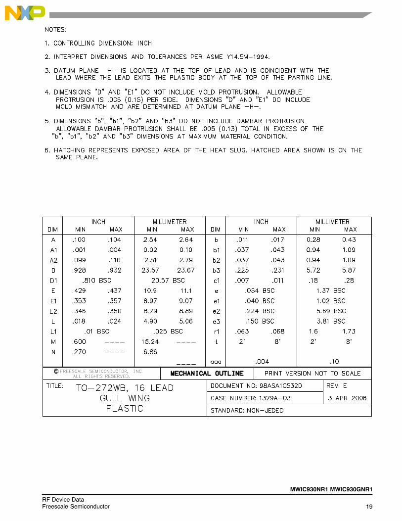
Embed Size (px)
Citation preview
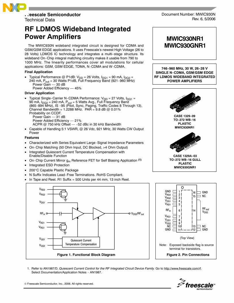
MWIC930NR1 MWIC930GNR1
1RF Device DataFreescale Semiconductor
RF LDMOS Wideband Integrated Power Amplifiers
The MWIC930N wideband integrated circuit is designed for CDMA andGSM/GSM EDGE applications. It uses Freescale�s newest High Voltage (26 to28 Volts) LDMOS IC technology and integrates a multi -stage structure. Itswideband On-Chip integral matching circuitry makes it usable from 790 to 1000 MHz. The linearity performances cover all modulations for cellularapplications: GSM, GSM EDGE, TDMA, N-CDMA and W-CDMA.
Final Application• Typical Performance @ P1dB: VDD = 26 Volts, IDQ1 = 90 mA, IDQ2 =
240 mA, Pout = 30 Watts P1dB, Full Frequency Band (921-960 MHz)Power Gain � 30 dBPower Added Efficiency � 45%
Driver Application
• Typical Single-Carrier N-CDMA Performance: VDD = 27 Volts, IDQ1 = 90 mA, IDQ2 = 240 mA, Pout = 5 Watts Avg., Full Frequency Band(865-894 MHz), IS -95 (Pilot, Sync, Paging, Traffic Codes 8 Through 13),Channel Bandwidth = 1.2288 MHz. PAR = 9.8 dB @ 0.01% Probability on CCDF.
Power Gain � 31 dBPower Added Efficiency � 21% ACPR @ 750 kHz Offset � -52 dBc in 30 kHz Bandwidth
• Capable of Handling 5:1 VSWR, @ 26 Vdc, 921 MHz, 30 Watts CW OutputPower
Features• Characterized with Series Equivalent Large-Signal Impedance Parameters• On-Chip Matching (50 Ohm Input, DC Blocked, >4 Ohm Output)• Integrated Quiescent Current Temperature Compensation with
Enable/Disable Function• On-Chip Current Mirror gm Reference FET for Self Biasing Application (1)
• Integrated ESD Protection
• 200°C Capable Plastic Package• N Suffix Indicates Lead-Free Terminations. RoHS Compliant.• In Tape and Reel. R1 Suffix = 500 Units per 44 mm, 13 inch Reel.
1. Refer to AN1987/D, Quiescent Current Control for the RF Integrated Circuit Device Family. Go to http://www.freescale.com/rf.Select Documentation/Application Notes - AN1987.
Document Number: MWIC930NRev. 6, 5/2006
Freescale SemiconductorTechnical Data
746-960 MHz, 30 W, 26-28 VSINGLE N-CDMA, GSM/GSM EDGE
RF LDMOS WIDEBAND INTEGRATEDPOWER AMPLIFIERS
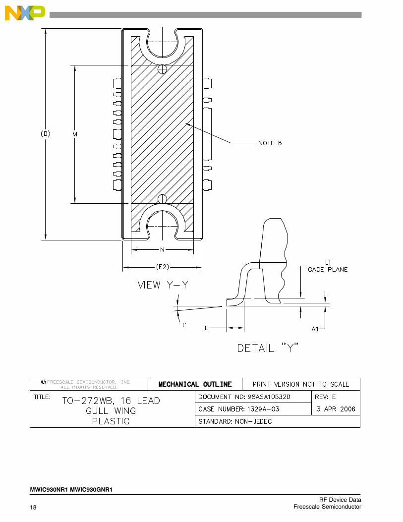
CASE 1329-09TO-272 WB-16
PLASTICMWIC930NR1
MWIC930NR1MWIC930GNR1
CASE 1329A-03TO-272 WB-16 GULL
PLASTICMWIC930GNR1
Figure 1. Functional Block Diagram Figure 2. Pin Connections
(Top View)
GND
VRD1
RFin
VGS1
GNDVRD2
RFout/VDS2
GND
VGS2
GND
VRG2VDS1
VRG1
NCNC
NC
VGS1
RFin
VDS1
VGS2
VDS2/RFout
Quiescent Current
Temperature Compensation
VRD2
VRG2 2345
6
78
16
15
14
1312
910
11
1
Note: Exposed backside flag is sourceterminal for transistors.
VRD1
VRG1
© Freescale Semiconductor, Inc., 2006. All rights reserved.
2RF Device Data
Freescale Semiconductor
MWIC930NR1 MWIC930GNR1
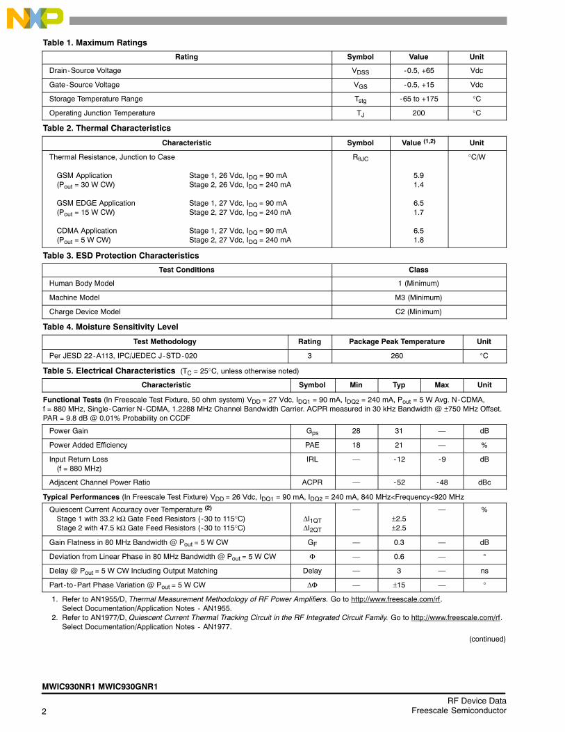
Table 1. Maximum Ratings
Rating Symbol Value Unit
Drain-Source Voltage VDSS -0.5, +65 Vdc
Gate-Source Voltage VGS -0.5, +15 Vdc
Storage Temperature Range Tstg -65 to +175 °C
Operating Junction Temperature TJ 200 °C
Table 2. Thermal Characteristics
Characteristic Symbol Value (1,2) Unit
Thermal Resistance, Junction to Case
GSM Application Stage 1, 26 Vdc, IDQ = 90 mA(Pout = 30 W CW) Stage 2, 26 Vdc, IDQ = 240 mA
GSM EDGE Application Stage 1, 27 Vdc, IDQ = 90 mA(Pout = 15 W CW) Stage 2, 27 Vdc, IDQ = 240 mA
CDMA Application Stage 1, 27 Vdc, IDQ = 90 mA(Pout = 5 W CW) Stage 2, 27 Vdc, IDQ = 240 mA
RθJC
5.91.4
6.51.7
6.51.8
°C/W
Table 3. ESD Protection Characteristics
Test Conditions Class
Human Body Model 1 (Minimum)
Machine Model M3 (Minimum)
Charge Device Model C2 (Minimum)
Table 4. Moisture Sensitivity Level
Test Methodology Rating Package Peak Temperature Unit
Per JESD 22-A113, IPC/JEDEC J-STD-020 3 260 °C
Table 5. Electrical Characteristics (TC = 25°C, unless otherwise noted)
Characteristic Symbol Min Typ Max Unit
Functional Tests (In Freescale Test Fixture, 50 ohm system) VDD = 27 Vdc, IDQ1 = 90 mA, IDQ2 = 240 mA, Pout = 5 W Avg. N-CDMA, f = 880 MHz, Single-Carrier N-CDMA, 1.2288 MHz Channel Bandwidth Carrier. ACPR measured in 30 kHz Bandwidth @ ±750 MHz Offset.PAR = 9.8 dB @ 0.01% Probability on CCDF
Power Gain Gps 28 31 � dB
Power Added Efficiency PAE 18 21 � %
Input Return Loss(f = 880 MHz)
IRL � -12 -9 dB
Adjacent Channel Power Ratio ACPR � -52 -48 dBc
Typical Performances (In Freescale Test Fixture) VDD = 26 Vdc, IDQ1 = 90 mA, IDQ2 = 240 mA, 840 MHz<Frequency<920 MHz
Quiescent Current Accuracy over Temperature (2)
Stage 1 with 33.2 kΩ Gate Feed Resistors ( -30 to 115°C) Stage 2 with 47.5 kΩ Gate Feed Resistors ( -30 to 115°C)
ΔI1QTΔI2QT
�±2.5±2.5
� %
Gain Flatness in 80 MHz Bandwidth @ Pout = 5 W CW GF � 0.3 � dB
Deviation from Linear Phase in 80 MHz Bandwidth @ Pout = 5 W CW Φ � 0.6 � °
Delay @ Pout = 5 W CW Including Output Matching Delay � 3 � ns
Part - to-Part Phase Variation @ Pout = 5 W CW ΔΦ � ±15 � °
1. Refer to AN1955/D, Thermal Measurement Methodology of RF Power Amplifiers. Go to http://www.freescale.com/rf. Select Documentation/Application Notes - AN1955.
2. Refer to AN1977/D, Quiescent Current Thermal Tracking Circuit in the RF Integrated Circuit Family. Go to http://www.freescale.com/rf.Select Documentation/Application Notes - AN1977.
(continued)

MWIC930NR1 MWIC930GNR1
3RF Device DataFreescale Semiconductor
Table 5. Electrical Characteristics (TC = 25°C, unless otherwise noted) (continued)
Characteristic Symbol Min Typ Max Unit
Typical GSM/GSM EDGE Performances (In Freescale GSM/GSM EDGE Test Fixture, 50 οhm system) VDD = 27 Vdc, IDQ1 = 90 mA, IDQ2 =240 mA, 921 MHz<Frequency<960 MHz
Output Power, 1dB Compression Point P1dB � 30 � W
Power Gain @ Pout = 30 W CW Gps � 30 � dB
Power Added Efficiency @ Pout = 30 W CW PAE � 45 � %
Input Return Loss @ Pout = 30 W CW IRL � -12 � dB
Intermodulation Distortion(15 W, 2-Tone, 100 kHz Tone Spacing)
IMD � -30 � dBc
Intermodulation Distortion(1 W, 2-Tone, 100 kHz Tone Spacing)
IMDbackoff
� -45 � dBc
Gain Flatness in 40 MHz Bandwidth @ Pout = 30 W CW GF � 0.3 � dB
Deviation from Linear Phase in 40 MHz Bandwidth @ Pout = 30 W CW Φ � 0.6 � °
4RF Device Data
Freescale Semiconductor
MWIC930NR1 MWIC930GNR1
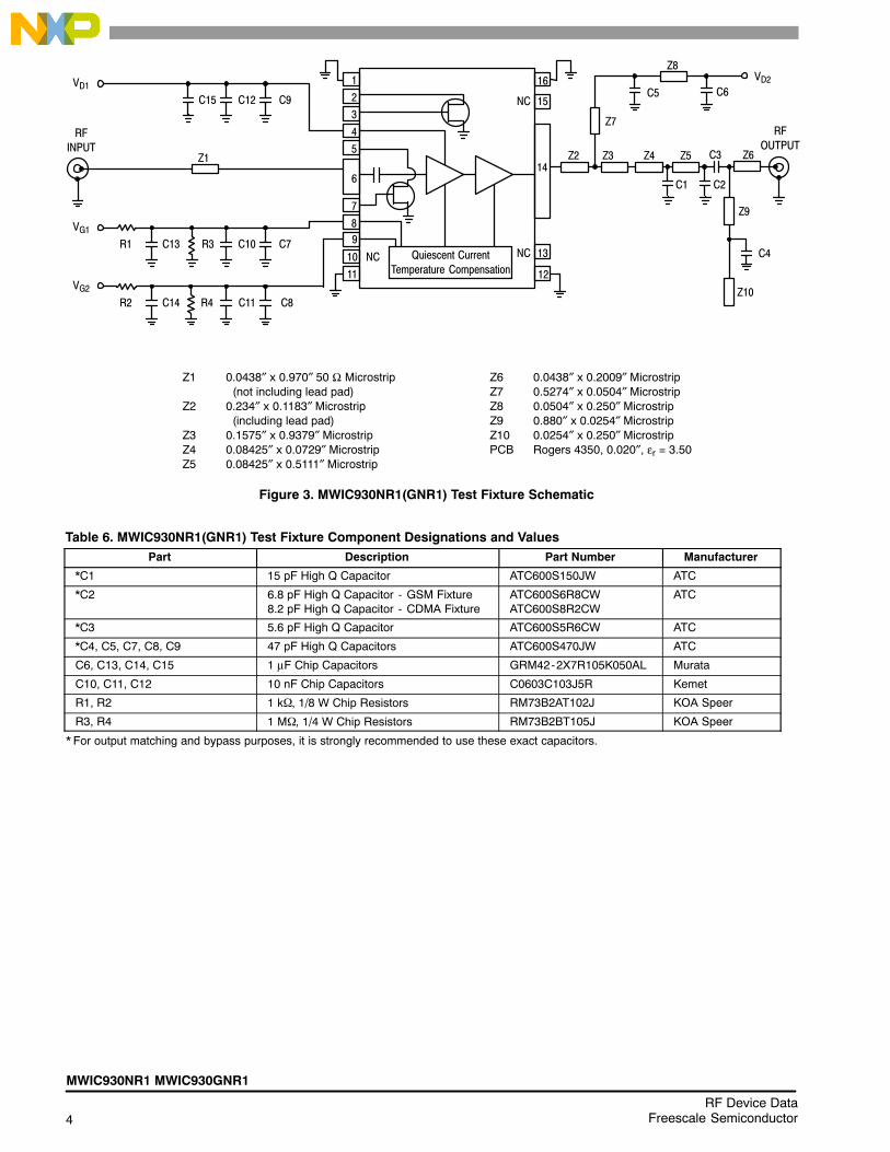
Z6 0.0438″ x 0.2009″ MicrostripZ7 0.5274″ x 0.0504″ MicrostripZ8 0.0504″ x 0.250″ MicrostripZ9 0.880″ x 0.0254″ MicrostripZ10 0.0254″ x 0.250″ MicrostripPCB Rogers 4350, 0.020″, εr = 3.50
Figure 3. MWIC930NR1(GNR1) Test Fixture Schematic
Z1 0.0438″ x 0.970″ 50 Ω Microstrip (not including lead pad)
Z2 0.234″ x 0.1183″ Microstrip (including lead pad)
Z3 0.1575″ x 0.9379″ MicrostripZ4 0.08425″ x 0.0729″ MicrostripZ5 0.08425″ x 0.5111″ Microstrip
RF
OUTPUTRF
INPUTZ1
VD2
Z8
Z7
C5 C6
VG1
R1 R3C13 C10 C7
Z2 Z3 Z4 Z5
Z9
Z10
C3
C4
C2C1
VG2
R2 R4C14 C11 C8
VD1
C15 C12 C9
1
2
3
4
5
6
7
8
14
13
1211
10
9
15
16
NC
NC
NCQuiescent Current
Temperature Compensation
Z6
Table 6. MWIC930NR1(GNR1) Test Fixture Component Designations and ValuesPart Description Part Number Manufacturer
*C1 15 pF High Q Capacitor ATC600S150JW ATC
*C2 6.8 pF High Q Capacitor - GSM Fixture8.2 pF High Q Capacitor - CDMA Fixture
ATC600S6R8CWATC600S8R2CW
ATC
*C3 5.6 pF High Q Capacitor ATC600S5R6CW ATC
*C4, C5, C7, C8, C9 47 pF High Q Capacitors ATC600S470JW ATC
C6, C13, C14, C15 1 μF Chip Capacitors GRM42-2X7R105K050AL Murata
C10, C11, C12 10 nF Chip Capacitors C0603C103J5R Kemet
R1, R2 1 k�, 1/8 W Chip Resistors RM73B2AT102J KOA Speer
R3, R4 1 M�, 1/4 W Chip Resistors RM73B2BT105J KOA Speer
* For output matching and bypass purposes, it is strongly recommended to use these exact capacitors.
MWIC930NR1 MWIC930GNR1
5RF Device DataFreescale Semiconductor
C15
VD2
VD1
RF
Input
RF
Output
C12
C9
C5
C6
C3
C2C1
C4
VG2
R2
R4
C14
VG1
R1
C13
R3C10
C11
C8
C7
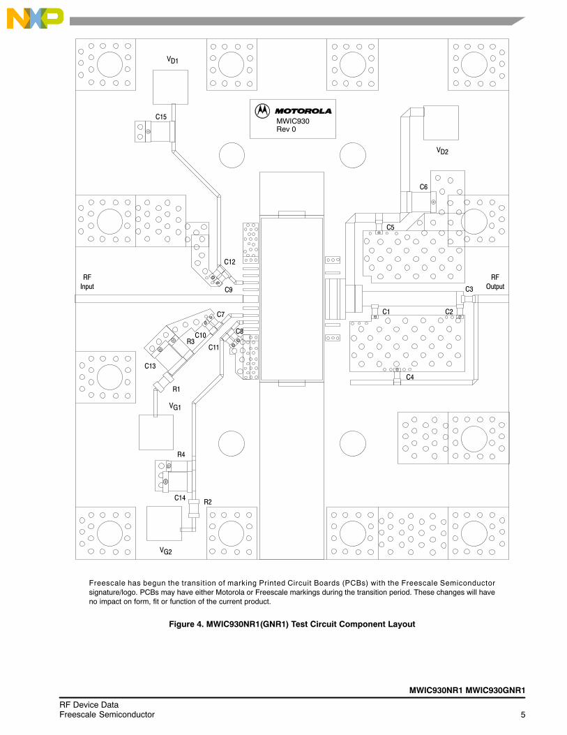
Figure 4. MWIC930NR1(GNR1) Test Circuit Component Layout
MWIC930Rev 0
Freescale has begun the transition of marking Printed Circuit Boards (PCBs) with the Freescale Semiconductorsignature/logo. PCBs may have either Motorola or Freescale markings during the transition period. These changes will haveno impact on form, fit or function of the current product.
6RF Device Data
Freescale Semiconductor
MWIC930NR1 MWIC930GNR1
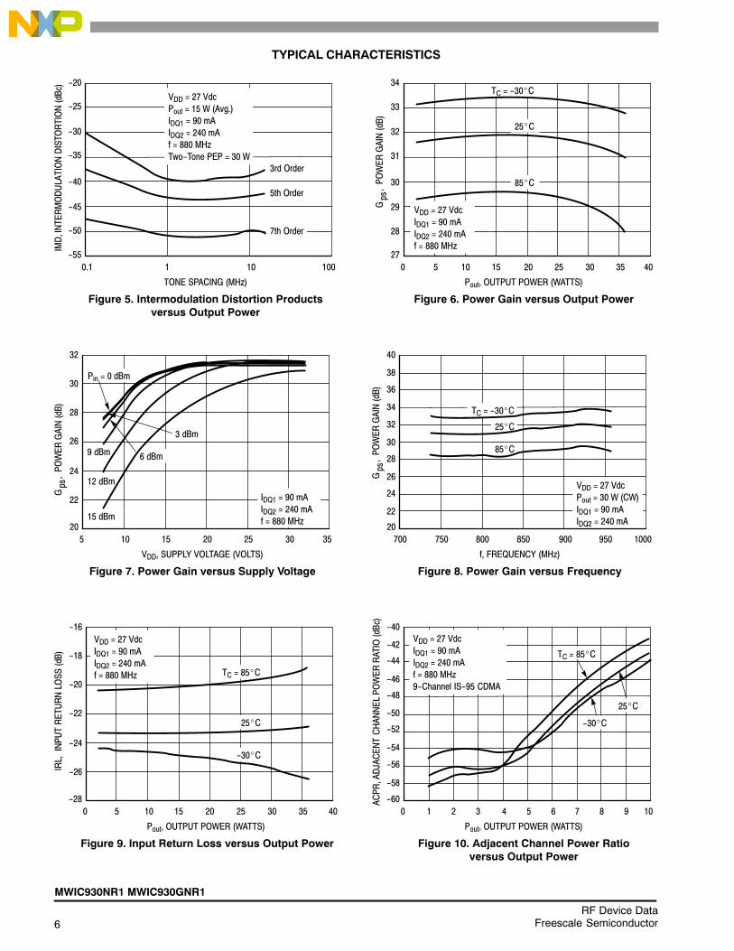
TYPICAL CHARACTERISTICS
100
−55
−20
0.1
7th Order
TONE SPACING (MHz)
Figure 5. Intermodulation Distortion Productsversus Output Power
INT
ER
MO
DU
LAT
ION
DIS
TO
RT
ION
(dB
c)IM
D,
VDD = 27 Vdc
Pout = 15 W (Avg.)
IDQ1 = 90 mA
IDQ2 = 240 mA
f = 880 MHz
Two−Tone PEP = 30 W
5th Order
3rd Order
−25
−30
−35
−40
−45
−50
1 10 40
27
34
0
25�C
Pout, OUTPUT POWER (WATTS)
Figure 6. Power Gain versus Output Power
Gps
, P
OW
ER
GA
IN (
dB)
VDD = 27 Vdc
IDQ1 = 90 mA
IDQ2 = 240 mA
f = 880 MHz
33
32
31
30
29
28
5 10 15 20 25 30 35
TC = −30�C
85�C
35
20
32
5
Pin = 0 dBm
VDD, SUPPLY VOLTAGE (VOLTS)
Figure 7. Power Gain versus Supply Voltage
Gps
, P
OW
ER
GA
IN (
dB)
IDQ1 = 90 mA
IDQ2 = 240 mA
f = 880 MHz
3025201510
30
28
26
24
22
6 dBm9 dBm
12 dBm
15 dBm
3 dBm
1000
20
40
700
f, FREQUENCY (MHz)
Figure 8. Power Gain versus Frequency
Gps
, P
OW
ER
GA
IN (
dB)
VDD = 27 Vdc
Pout = 30 W (CW)
IDQ1 = 90 mA
IDQ2 = 240 mA
25�C
TC = −30�C
85�C
38
36
34
32
30
28
26
24
22
750 800 850 900 950
40
−28
−16
0
Pout, OUTPUT POWER (WATTS)
Figure 9. Input Return Loss versus Output Power
INP
UT
RE
TU
RN
LO
SS
(dB
)IR
L,
VDD = 27 Vdc
IDQ1 = 90 mA
IDQ2 = 240 mA
f = 880 MHz
−30�C
TC = 85�C
−18
−20
−22
−24
−26
5 10 15 20 25 30 35
25�C
10
−60
−40
0
Pout, OUTPUT POWER (WATTS)
Figure 10. Adjacent Channel Power Ratioversus Output Power
AC
PR
, AD
JAC
EN
T C
HA
NN
EL
PO
WE
R R
AT
IO (
dBc)
−42
−44
−46
−48
−50
−52
−54
−56
−58
1 2 3 4 5 6 7 8 9
VDD = 27 Vdc
IDQ1 = 90 mA
IDQ2 = 240 mA
f = 880 MHz
9−Channel IS−95 CDMA
25�C
−30�C
TC = 85�C
MWIC930NR1 MWIC930GNR1
7RF Device DataFreescale Semiconductor
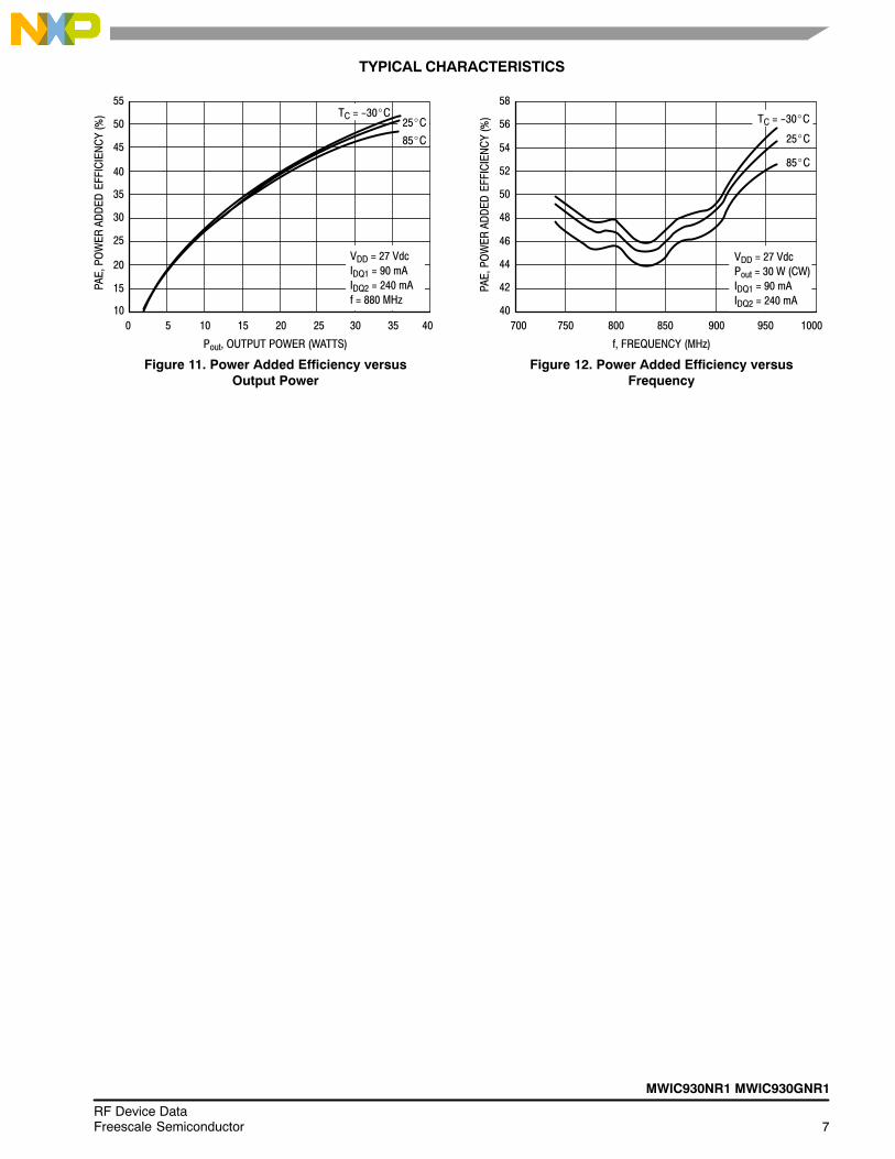
TYPICAL CHARACTERISTICS
40
10
55
0
Pout, OUTPUT POWER (WATTS)
Figure 11. Power Added Efficiency versusOutput Power
PA
E, P
OW
ER
AD
DE
D E
FF
ICIE
NC
Y (
%)
50
45
40
35
30
25
20
15
5 10 15 20 25 30 35
25�CTC = −30�C
85�C
1000
40
58
700
f, FREQUENCY (MHz)
Figure 12. Power Added Efficiency versusFrequency
750 800 850 900 950
56
54
52
50
48
46
44
42PA
E, P
OW
ER
AD
DE
D E
FF
ICIE
NC
Y (
%)
VDD = 27 Vdc
IDQ1 = 90 mA
IDQ2 = 240 mA
f = 880 MHz
25�C
TC = −30�C
85�C
VDD = 27 Vdc
Pout = 30 W (CW)
IDQ1 = 90 mA
IDQ2 = 240 mA
8RF Device Data
Freescale Semiconductor
MWIC930NR1 MWIC930GNR1
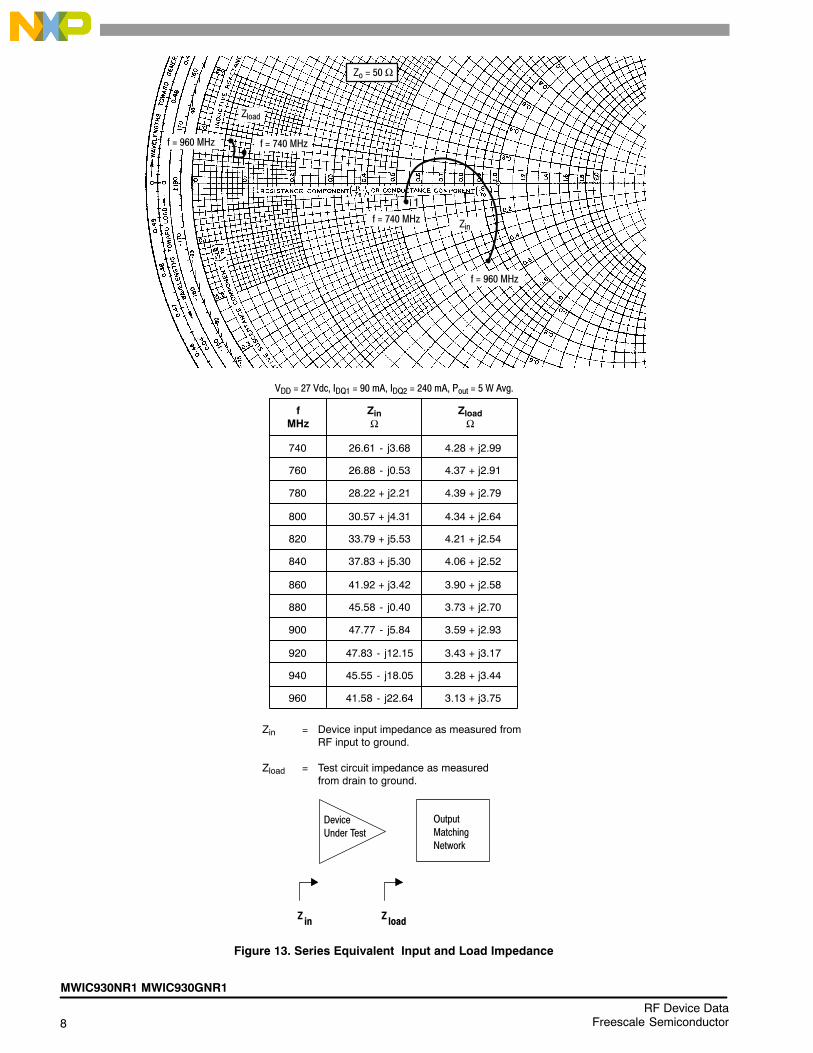
Figure 13. Series Equivalent Input and Load Impedance
fMHz
ZinΩ
ZloadΩ
740
760
780
26.61 - j3.68
28.22 + j2.21
26.88 - j0.53
4.28 + j2.99
4.37 + j2.91
4.39 + j2.79
VDD = 27 Vdc, IDQ1 = 90 mA, IDQ2 = 240 mA, Pout = 5 W Avg.
Zin = Device input impedance as measured from RF input to ground.
Zload = Test circuit impedance as measured from drain to ground.
Zin
Zload
Device
Under Test
Output
Matching
Network
800
820
840
30.57 + j4.31
37.83 + j5.30
33.79 + j5.53
4.34 + j2.64
4.21 + j2.54
4.06 + j2.52
860
880
900
41.92 + j3.42
47.77 - j5.84
45.58 - j0.40
3.90 + j2.58
3.73 + j2.70
3.59 + j2.93
920
940
960
47.83 - j12.15
41.58 - j22.64
45.55 - j18.05
3.43 + j3.17
3.28 + j3.44
3.13 + j3.75
1
f = 960 MHz
f = 740 MHz
Zo = 50 Ω
Zin
Zload
f = 960 MHz f = 740 MHz
MWIC930NR1 MWIC930GNR1
9RF Device DataFreescale Semiconductor
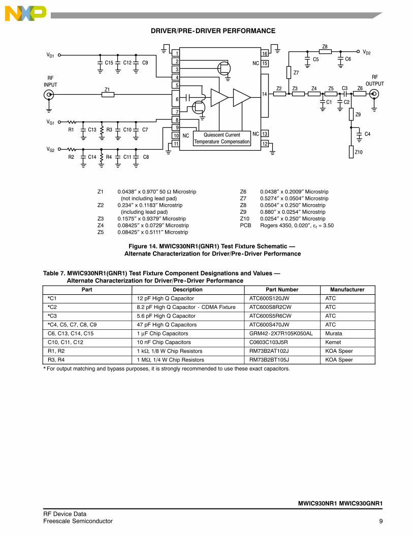
DRIVER/PRE-DRIVER PERFORMANCE
Z6 0.0438″ x 0.2009″ MicrostripZ7 0.5274″ x 0.0504″ MicrostripZ8 0.0504″ x 0.250″ MicrostripZ9 0.880″ x 0.0254″ MicrostripZ10 0.0254″ x 0.250″ MicrostripPCB Rogers 4350, 0.020″, εr = 3.50
Figure 14. MWIC930NR1(GNR1) Test Fixture Schematic � Alternate Characterization for Driver/Pre-Driver Performance
Z1 0.0438″ x 0.970″ 50 Ω Microstrip (not including lead pad)
Z2 0.234″ x 0.1183″ Microstrip (including lead pad)
Z3 0.1575″ x 0.9379″ MicrostripZ4 0.08425″ x 0.0729″ MicrostripZ5 0.08425″ x 0.5111″ Microstrip
RF
OUTPUTRF
INPUTZ1
VD2
Z8
Z7
C5 C6
VG1
R1 R3C13 C10 C7
Z2 Z3 Z4 Z5
Z9
Z10
C3
C4
C2C1
VG2
R2 R4C14 C11 C8
VD1
C15 C12 C9
1
2
3
4
5
6
7
8
14
13
1211
10
9
15
16
NC
NC
NCQuiescent Current
Temperature Compensation
Z6
Table 7. MWIC930NR1(GNR1) Test Fixture Component Designations and Values � Alternate Characterization for Driver/Pre-Driver Performance
Part Description Part Number Manufacturer
*C1 12 pF High Q Capacitor ATC600S120JW ATC
*C2 8.2 pF High Q Capacitor - CDMA Fixture ATC600S8R2CW ATC
*C3 5.6 pF High Q Capacitor ATC600S5R6CW ATC
*C4, C5, C7, C8, C9 47 pF High Q Capacitors ATC600S470JW ATC
C6, C13, C14, C15 1 μF Chip Capacitors GRM42-2X7R105K050AL Murata
C10, C11, C12 10 nF Chip Capacitors C0603C103J5R Kemet
R1, R2 1 k�, 1/8 W Chip Resistors RM73B2AT102J KOA Speer
R3, R4 1 M�, 1/4 W Chip Resistors RM73B2BT105J KOA Speer
* For output matching and bypass purposes, it is strongly recommended to use these exact capacitors.
10RF Device Data
Freescale Semiconductor
MWIC930NR1 MWIC930GNR1
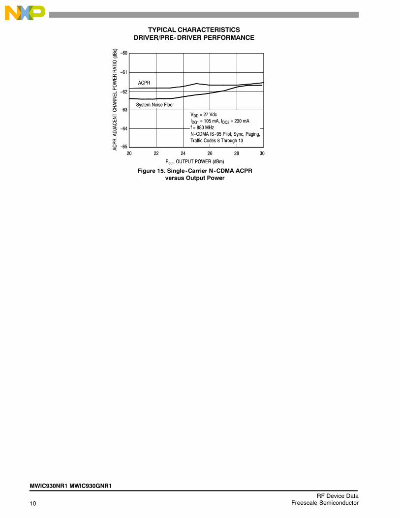
TYPICAL CHARACTERISTICSDRIVER/PRE-DRIVER PERFORMANCE
30
−65
−60
20
System Noise Floor
Pout, OUTPUT POWER (dBm)
Figure 15. Single-Carrier N-CDMA ACPRversus Output Power
AC
PR
, AD
JAC
EN
T C
HA
NN
EL
PO
WE
R R
AT
IO (
dBc)
VDD = 27 Vdc
IDQ1 = 105 mA, IDQ2 = 230 mA
f = 880 MHz
N−CDMA IS−95 Pilot, Sync, Paging,
Traffic Codes 8 Through 13
ACPR
−61
−62
−63
−64
22 24 26 28
MWIC930NR1 MWIC930GNR1
11RF Device DataFreescale Semiconductor
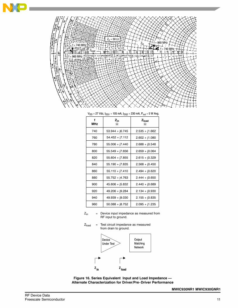
f = 960 MHzf = 740 MHz
Zo = 50 ΩZin
Zload
Figure 16. Series Equivalent Input and Load Impedance �Alternate Characterization for Driver/Pre-Driver Performance
fMHz
ZinΩ
ZloadΩ
740
760
780
53.944 + j6.745
55.006 + j7.440
54.452 + j7.112
2.535 + j1.662
2.602 + j1.080
2.688 + j0.548
VDD = 27 Vdc, IDQ1 = 105 mA, IDQ2 = 230 mA, Pout = 5 W Avg.
Zin = Device input impedance as measured from RF input to ground.
Zload = Test circuit impedance as measured from drain to ground.
Zin
Zload
Device
Under Test
Output
Matching
Network
800
820
840
55.549 + j7.656
55.190 + j7.835
55.604 + j7.855
2.659 + j0.064
2.615 + j0.329
2.568 + j0.450
860
880
900
55.110 + j7.410
45.606 + j5.832
55.752 + j4.763
2.494 + j0.620
2.444 + j0.650
2.440 + j0.689
920
940
960
49.206 + j9.284
50.088 + j8.752
49.939 + j9.030
2.134 + j0.930
2.155 + j0.835
2.095 + j1.235
f = 740 MHz
f = 960 MHz

12RF Device Data
Freescale Semiconductor
MWIC930NR1 MWIC930GNR1
NOTES

MWIC930NR1 MWIC930GNR1
13RF Device DataFreescale Semiconductor
NOTES
14RF Device Data
Freescale Semiconductor
MWIC930NR1 MWIC930GNR1
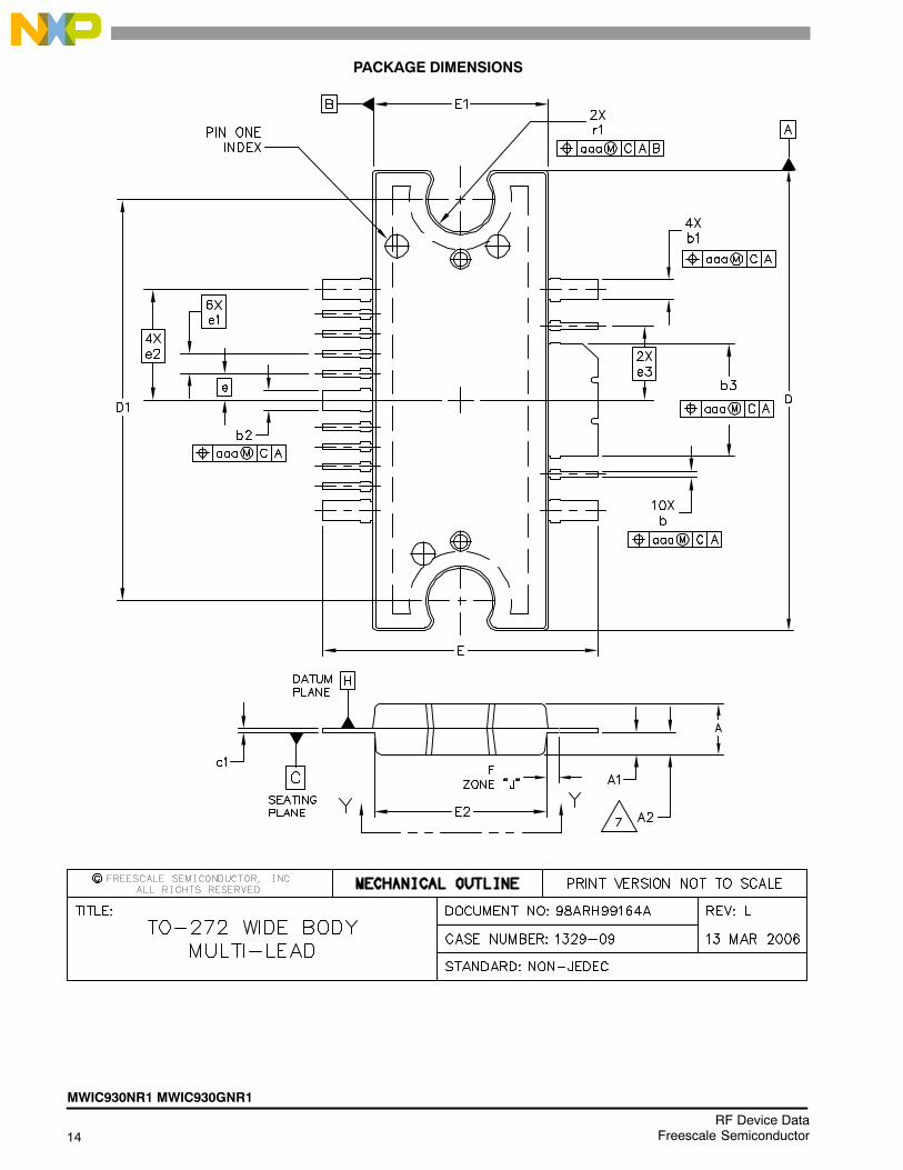
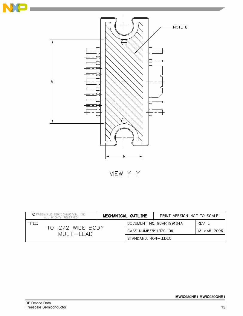
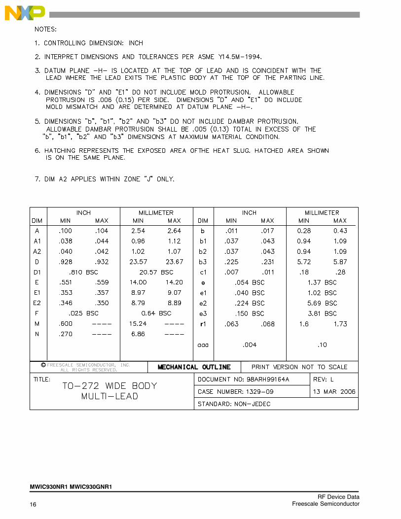
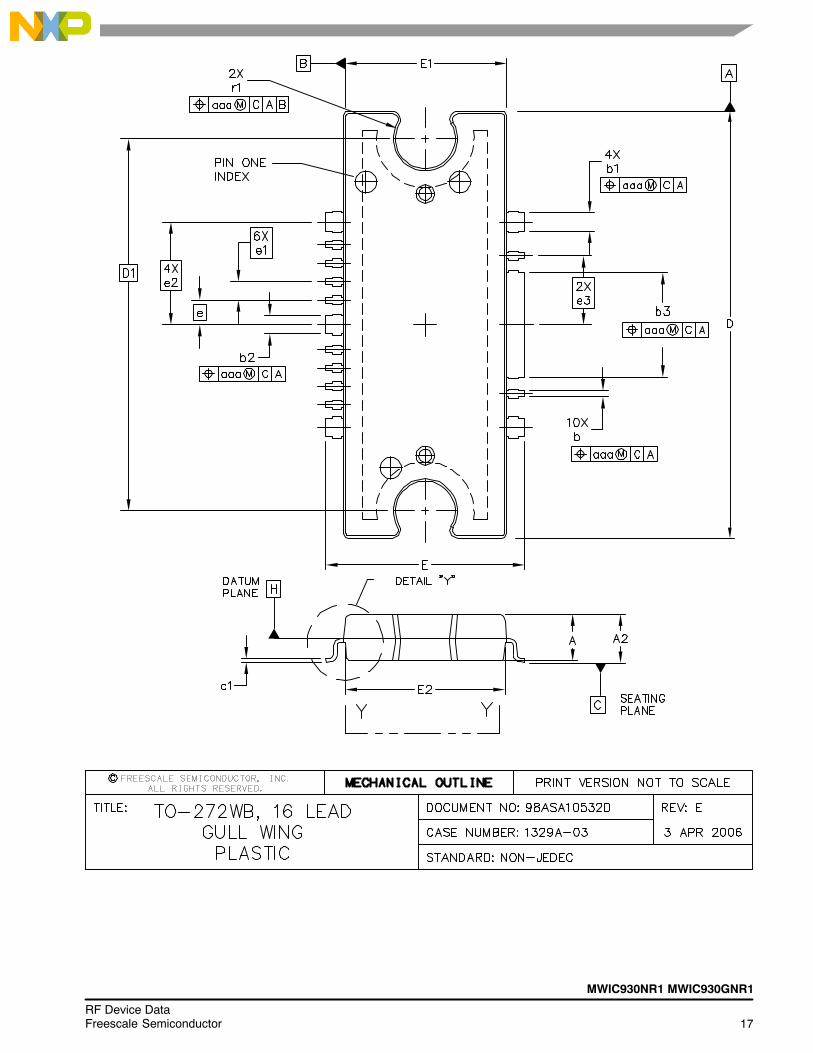
PACKAGE DIMENSIONS
MWIC930NR1 MWIC930GNR1
15RF Device DataFreescale Semiconductor
16RF Device Data
Freescale Semiconductor
MWIC930NR1 MWIC930GNR1
MWIC930NR1 MWIC930GNR1
17RF Device DataFreescale Semiconductor
18RF Device Data
Freescale Semiconductor
MWIC930NR1 MWIC930GNR1
MWIC930NR1 MWIC930GNR1
19RF Device DataFreescale Semiconductor

20RF Device Data
Freescale Semiconductor
MWIC930NR1 MWIC930GNR1
Information in this document is provided solely to enable system and softwareimplementers to use Freescale Semiconductor products. There are no express orimplied copyright licenses granted hereunder to design or fabricate any integratedcircuits or integrated circuits based on the information in this document.
Freescale Semiconductor reserves the right to make changes without further notice toany products herein. Freescale Semiconductor makes no warranty, representation orguarantee regarding the suitability of its products for any particular purpose, nor doesFreescale Semiconductor assume any liability arising out of the application or use ofany product or circuit, and specifically disclaims any and all liability, including withoutlimitation consequential or incidental damages. �Typical� parameters that may beprovided in Freescale Semiconductor data sheets and/or specifications can and dovary in different applications and actual performance may vary over time. All operatingparameters, including �Typicals�, must be validated for each customer application bycustomer�s technical experts. Freescale Semiconductor does not convey any licenseunder its patent rights nor the rights of others. Freescale Semiconductor products arenot designed, intended, or authorized for use as components in systems intended forsurgical implant into the body, or other applications intended to support or sustain life,or for any other application in which the failure of the Freescale Semiconductor productcould create a situation where personal injury or death may occur. Should Buyerpurchase or use Freescale Semiconductor products for any such unintended orunauthorized application, Buyer shall indemnify and hold Freescale Semiconductorand its officers, employees, subsidiaries, affiliates, and distributors harmless against allclaims, costs, damages, and expenses, and reasonable attorney fees arising out of,directly or indirectly, any claim of personal injury or death associated with suchunintended or unauthorized use, even if such claim alleges that FreescaleSemiconductor was negligent regarding the design or manufacture of the part.
Freescale� and the Freescale logo are trademarks of Freescale Semiconductor, Inc.All other product or service names are the property of their respective owners.© Freescale Semiconductor, Inc. 2006. All rights reserved.
How to Reach Us:
Home Page:www.freescale.com
E-mail:[email protected]
USA/Europe or Locations Not Listed:Freescale SemiconductorTechnical Information Center, CH3701300 N. Alma School RoadChandler, Arizona 85224+1-800-521-6274 or [email protected]
Europe, Middle East, and Africa:Freescale Halbleiter Deutschland GmbHTechnical Information CenterSchatzbogen 781829 Muenchen, Germany+44 1296 380 456 (English)+46 8 52200080 (English)+49 89 92103 559 (German)+33 1 69 35 48 48 (French)[email protected]
Japan:Freescale Semiconductor Japan Ltd.HeadquartersARCO Tower 15F1-8-1, Shimo-Meguro, Meguro-ku,Tokyo 153-0064Japan0120 191014 or +81 3 5437 [email protected]
Asia/Pacific:Freescale Semiconductor Hong Kong Ltd.Technical Information Center2 Dai King StreetTai Po Industrial EstateTai Po, N.T., Hong Kong+800 2666 [email protected]
For Literature Requests Only:Freescale Semiconductor Literature Distribution CenterP.O. Box 5405Denver, Colorado 802171-800-441-2447 or 303-675-2140Fax: [email protected]
Document Number: MWIC930NRev. 6, 5/2006
RoHS-compliant and/or Pb-free versions of Freescale products have the functionality and electricalcharacteristics of their non-RoHS-compliant and/or non-Pb-free counterparts. For furtherinformation, see http://www.freescale.com or contact your Freescale sales representative.
For information on Freescale�s Environmental Products program, go to http://www.freescale.com/epp.