Embed Size (px)
Citation preview

IBM
Technical Information Manual PC 300GL (6272 and 6282)


IBM Technical Information Manual PC 300GL (6272 and 6282)

Note
Before using this information and the product it supports, be sure to read the general information underAppendix E, “Notices and Trademarks” on page 55.
First Edition (October 1997)
The following paragraph does not apply to the United Kingdom or any country where such provisions are inconsistent withlocal law: INTERNATIONAL BUSINESS MACHINES CORPORATION PROVIDES THIS PUBLICATION “AS IS” WITHOUTWARRANTY OF ANY KIND, EITHER EXPRESS OR IMPLIED, INCLUDING, BUT NOT LIMITED TO, THE IMPLIED WARRANTIESOF MERCHANTABILITY OR FITNESS FOR A PARTICULAR PURPOSE. Some states do not allow disclaimer of express or impliedwarranties in certain transactions, therefore, this statement may not apply to you.
This publication could include technical inaccuracies or typographical errors. Changes are periodically made to the informationherein; these changes will be incorporated in new editions of the publication. IBM may make improvements and/or changes in theproduct(s) and/or the program(s) described in this publication at any time.
This publication was developed for products and services offered in the United States of America. IBM may not offer the products,services, or features discussed in this document in other countries, and the information is subject to change without notice. Consultyour local IBM representative for information on the products, services, and features available in your area.
Requests for technical information about IBM products should be made to your IBM reseller or IBM marketing representative.
Copyright International Business Machines Corporation October 1997. All rights reserved.Note to U.S. Government Users — Documentation related to restricted rights — Use, duplication or disclosure is subject torestrictions set forth in GSA ADP Schedule Contract with IBM Corp.

Contents
Preface . . . . . . . . . . . . . . . . . . . . . . . . . . . . . . . . . . . . . . . . . . . . . . . . . . . . . . . vRelated Publications . . . . . . . . . . . . . . . . . . . . . . . . . . . . . . . . . . . . . . . . . . . . . . . . viManual Style . . . . . . . . . . . . . . . . . . . . . . . . . . . . . . . . . . . . . . . . . . . . . . . . . . . . vii
Chapter 1. System Overview . . . . . . . . . . . . . . . . . . . . . . . . . . . . . . . . . . . . . . . . . . 1Major Features . . . . . . . . . . . . . . . . . . . . . . . . . . . . . . . . . . . . . . . . . . . . . . . . . . . 1Other Features . . . . . . . . . . . . . . . . . . . . . . . . . . . . . . . . . . . . . . . . . . . . . . . . . . . 2
Wake on LAN . . . . . . . . . . . . . . . . . . . . . . . . . . . . . . . . . . . . . . . . . . . . . . . . . . 2Wake Up On Ring . . . . . . . . . . . . . . . . . . . . . . . . . . . . . . . . . . . . . . . . . . . . . . . . 2Network Enablement . . . . . . . . . . . . . . . . . . . . . . . . . . . . . . . . . . . . . . . . . . . . . . 2
Chapter 2. System Board Features . . . . . . . . . . . . . . . . . . . . . . . . . . . . . . . . . . . . . . 3Microprocessor . . . . . . . . . . . . . . . . . . . . . . . . . . . . . . . . . . . . . . . . . . . . . . . . . . . 3Chipset Control . . . . . . . . . . . . . . . . . . . . . . . . . . . . . . . . . . . . . . . . . . . . . . . . . . . 4
L2 Cache . . . . . . . . . . . . . . . . . . . . . . . . . . . . . . . . . . . . . . . . . . . . . . . . . . . . . 4System Memory . . . . . . . . . . . . . . . . . . . . . . . . . . . . . . . . . . . . . . . . . . . . . . . . . 5PCI Bus . . . . . . . . . . . . . . . . . . . . . . . . . . . . . . . . . . . . . . . . . . . . . . . . . . . . . . 6Bus Master IDE Interface . . . . . . . . . . . . . . . . . . . . . . . . . . . . . . . . . . . . . . . . . . . 6PCI to ISA Bridge . . . . . . . . . . . . . . . . . . . . . . . . . . . . . . . . . . . . . . . . . . . . . . . . 6USB Interface . . . . . . . . . . . . . . . . . . . . . . . . . . . . . . . . . . . . . . . . . . . . . . . . . . 7
Video Subsystem . . . . . . . . . . . . . . . . . . . . . . . . . . . . . . . . . . . . . . . . . . . . . . . . . . 8Cirrus CL-GD5446 Chip . . . . . . . . . . . . . . . . . . . . . . . . . . . . . . . . . . . . . . . . . . . . 8Video Memory . . . . . . . . . . . . . . . . . . . . . . . . . . . . . . . . . . . . . . . . . . . . . . . . . . 8
Input/Output Controller . . . . . . . . . . . . . . . . . . . . . . . . . . . . . . . . . . . . . . . . . . . . . . . 9Diskette Drive Support . . . . . . . . . . . . . . . . . . . . . . . . . . . . . . . . . . . . . . . . . . . . . 9Serial Port . . . . . . . . . . . . . . . . . . . . . . . . . . . . . . . . . . . . . . . . . . . . . . . . . . . . 9Parallel Port . . . . . . . . . . . . . . . . . . . . . . . . . . . . . . . . . . . . . . . . . . . . . . . . . . . 10Keyboard and Mouse Ports . . . . . . . . . . . . . . . . . . . . . . . . . . . . . . . . . . . . . . . . . . 10Network Connection . . . . . . . . . . . . . . . . . . . . . . . . . . . . . . . . . . . . . . . . . . . . . . 11General Purpose I/O Ports . . . . . . . . . . . . . . . . . . . . . . . . . . . . . . . . . . . . . . . . . . . 11Real-Time Clock and CMOS . . . . . . . . . . . . . . . . . . . . . . . . . . . . . . . . . . . . . . . . . . 11
Flash EEPROM . . . . . . . . . . . . . . . . . . . . . . . . . . . . . . . . . . . . . . . . . . . . . . . . . . . 12Riser Card . . . . . . . . . . . . . . . . . . . . . . . . . . . . . . . . . . . . . . . . . . . . . . . . . . . . . . 12Physical Layout . . . . . . . . . . . . . . . . . . . . . . . . . . . . . . . . . . . . . . . . . . . . . . . . . . . 13
System Board . . . . . . . . . . . . . . . . . . . . . . . . . . . . . . . . . . . . . . . . . . . . . . . . . . 13Jumpers . . . . . . . . . . . . . . . . . . . . . . . . . . . . . . . . . . . . . . . . . . . . . . . . . . . . . 14Switches . . . . . . . . . . . . . . . . . . . . . . . . . . . . . . . . . . . . . . . . . . . . . . . . . . . . . 14Connectivity . . . . . . . . . . . . . . . . . . . . . . . . . . . . . . . . . . . . . . . . . . . . . . . . . . . 15
Chapter 3. Physical Specifications . . . . . . . . . . . . . . . . . . . . . . . . . . . . . . . . . . . . . . 16PC 300GL 6272 . . . . . . . . . . . . . . . . . . . . . . . . . . . . . . . . . . . . . . . . . . . . . . . . . . 17PC 300GL 6282 . . . . . . . . . . . . . . . . . . . . . . . . . . . . . . . . . . . . . . . . . . . . . . . . . . 19
Chapter 4. Power Supply . . . . . . . . . . . . . . . . . . . . . . . . . . . . . . . . . . . . . . . . . . . . 21Power Input . . . . . . . . . . . . . . . . . . . . . . . . . . . . . . . . . . . . . . . . . . . . . . . . . . . . . 21Power Output . . . . . . . . . . . . . . . . . . . . . . . . . . . . . . . . . . . . . . . . . . . . . . . . . . . . 22
PC 300GL 6272 . . . . . . . . . . . . . . . . . . . . . . . . . . . . . . . . . . . . . . . . . . . . . . . . . 22PC 300GL 6282 . . . . . . . . . . . . . . . . . . . . . . . . . . . . . . . . . . . . . . . . . . . . . . . . . 22
Component Outputs . . . . . . . . . . . . . . . . . . . . . . . . . . . . . . . . . . . . . . . . . . . . . . . . 23Output Protection . . . . . . . . . . . . . . . . . . . . . . . . . . . . . . . . . . . . . . . . . . . . . . . . . . 24
Copyright IBM Corp. October 1997 iii

Connector Description . . . . . . . . . . . . . . . . . . . . . . . . . . . . . . . . . . . . . . . . . . . . . . . 24
Chapter 5. System Software . . . . . . . . . . . . . . . . . . . . . . . . . . . . . . . . . . . . . . . . . . 25BIOS . . . . . . . . . . . . . . . . . . . . . . . . . . . . . . . . . . . . . . . . . . . . . . . . . . . . . . . . . 25Plug and Play . . . . . . . . . . . . . . . . . . . . . . . . . . . . . . . . . . . . . . . . . . . . . . . . . . . . 25POST . . . . . . . . . . . . . . . . . . . . . . . . . . . . . . . . . . . . . . . . . . . . . . . . . . . . . . . . 25Configuration/Setup Utility . . . . . . . . . . . . . . . . . . . . . . . . . . . . . . . . . . . . . . . . . . . . . 25Advanced Power Management (APM) . . . . . . . . . . . . . . . . . . . . . . . . . . . . . . . . . . . . . . 26Flash Update Utility . . . . . . . . . . . . . . . . . . . . . . . . . . . . . . . . . . . . . . . . . . . . . . . . 26Diagnostic Programs . . . . . . . . . . . . . . . . . . . . . . . . . . . . . . . . . . . . . . . . . . . . . . . . 26
Chapter 6. System Compatibility . . . . . . . . . . . . . . . . . . . . . . . . . . . . . . . . . . . . . . . 27Hardware Compatibility . . . . . . . . . . . . . . . . . . . . . . . . . . . . . . . . . . . . . . . . . . . . . . 27
Hardware Interrupts . . . . . . . . . . . . . . . . . . . . . . . . . . . . . . . . . . . . . . . . . . . . . . . 28Diskette Drives and Controller . . . . . . . . . . . . . . . . . . . . . . . . . . . . . . . . . . . . . . . . . 29Hard Disk Drives and Controller . . . . . . . . . . . . . . . . . . . . . . . . . . . . . . . . . . . . . . . . 29
Software Compatibility . . . . . . . . . . . . . . . . . . . . . . . . . . . . . . . . . . . . . . . . . . . . . . . 30Software Interrupts . . . . . . . . . . . . . . . . . . . . . . . . . . . . . . . . . . . . . . . . . . . . . . . 30Machine-Sensitive Programs . . . . . . . . . . . . . . . . . . . . . . . . . . . . . . . . . . . . . . . . . 30
Appendix A. Connector Pin Assignments . . . . . . . . . . . . . . . . . . . . . . . . . . . . . . . . . . 31System Memory Connector . . . . . . . . . . . . . . . . . . . . . . . . . . . . . . . . . . . . . . . . . . . . 32IDE Connectors . . . . . . . . . . . . . . . . . . . . . . . . . . . . . . . . . . . . . . . . . . . . . . . . . . . 34USB Connectors . . . . . . . . . . . . . . . . . . . . . . . . . . . . . . . . . . . . . . . . . . . . . . . . . . 35Monitor Connector . . . . . . . . . . . . . . . . . . . . . . . . . . . . . . . . . . . . . . . . . . . . . . . . . 35Diskette Drive Connector . . . . . . . . . . . . . . . . . . . . . . . . . . . . . . . . . . . . . . . . . . . . . 35Serial Port Connectors . . . . . . . . . . . . . . . . . . . . . . . . . . . . . . . . . . . . . . . . . . . . . . . 37Parallel Port Connector . . . . . . . . . . . . . . . . . . . . . . . . . . . . . . . . . . . . . . . . . . . . . . 37Keyboard and Mouse Port Connectors . . . . . . . . . . . . . . . . . . . . . . . . . . . . . . . . . . . . . 38ISA Connectors . . . . . . . . . . . . . . . . . . . . . . . . . . . . . . . . . . . . . . . . . . . . . . . . . . . 39PCI Connector . . . . . . . . . . . . . . . . . . . . . . . . . . . . . . . . . . . . . . . . . . . . . . . . . . . 41Wake on LAN and Modem/Ring Wakeup Connectors . . . . . . . . . . . . . . . . . . . . . . . . . . . . . 43Power Supply Connectors . . . . . . . . . . . . . . . . . . . . . . . . . . . . . . . . . . . . . . . . . . . . . 43
Appendix B. System Address Maps . . . . . . . . . . . . . . . . . . . . . . . . . . . . . . . . . . . . . 44System Memory Map . . . . . . . . . . . . . . . . . . . . . . . . . . . . . . . . . . . . . . . . . . . . . . . 44Input/Output Address Map . . . . . . . . . . . . . . . . . . . . . . . . . . . . . . . . . . . . . . . . . . . . 45DMA I/O Address Map . . . . . . . . . . . . . . . . . . . . . . . . . . . . . . . . . . . . . . . . . . . . . . . 48
Appendix C. IRQ and DMA Channel Assignments . . . . . . . . . . . . . . . . . . . . . . . . . . . . 50
Appendix D. Error Codes . . . . . . . . . . . . . . . . . . . . . . . . . . . . . . . . . . . . . . . . . . . . 52POST Error Codes . . . . . . . . . . . . . . . . . . . . . . . . . . . . . . . . . . . . . . . . . . . . . . . . . 52Beep Codes . . . . . . . . . . . . . . . . . . . . . . . . . . . . . . . . . . . . . . . . . . . . . . . . . . . . . 54
Appendix E. Notices and Trademarks . . . . . . . . . . . . . . . . . . . . . . . . . . . . . . . . . . . . 55
References . . . . . . . . . . . . . . . . . . . . . . . . . . . . . . . . . . . . . . . . . . . . . . . . . . . . . 56
Index . . . . . . . . . . . . . . . . . . . . . . . . . . . . . . . . . . . . . . . . . . . . . . . . . . . . . . . . . 57
iv Technical Information Manual

Figures
1. L2 Cache Characteristics . . . . . . . . . . . . . . . . . . . . . . . . . . . . . . . . . . . . . . . . . . 42. L2 Cache Timings . . . . . . . . . . . . . . . . . . . . . . . . . . . . . . . . . . . . . . . . . . . . . . 43. System Memory Configuration . . . . . . . . . . . . . . . . . . . . . . . . . . . . . . . . . . . . . . . 54. Serial Port Assignments . . . . . . . . . . . . . . . . . . . . . . . . . . . . . . . . . . . . . . . . . . 95. Parallel Port Assignments . . . . . . . . . . . . . . . . . . . . . . . . . . . . . . . . . . . . . . . . . 106. Riser Card Characteristics . . . . . . . . . . . . . . . . . . . . . . . . . . . . . . . . . . . . . . . . . 127. J6 CMOS Clear/Password Jumper . . . . . . . . . . . . . . . . . . . . . . . . . . . . . . . . . . . . 148. Microprocessor Speed (SW1 1-4) . . . . . . . . . . . . . . . . . . . . . . . . . . . . . . . . . . . . . 149. Ethernet Disable/Enable (SW1 5) . . . . . . . . . . . . . . . . . . . . . . . . . . . . . . . . . . . . . 14
10. Diskette-Write Protection (SW1 6) . . . . . . . . . . . . . . . . . . . . . . . . . . . . . . . . . . . . . 1411. Size (PC 300GL 6272) . . . . . . . . . . . . . . . . . . . . . . . . . . . . . . . . . . . . . . . . . . . 1712. Weight (PC 300GL 6272) . . . . . . . . . . . . . . . . . . . . . . . . . . . . . . . . . . . . . . . . . 1713. Cables (PC 300GL 6272) . . . . . . . . . . . . . . . . . . . . . . . . . . . . . . . . . . . . . . . . . 1714. Air Temperature (PC 300GL 6272) . . . . . . . . . . . . . . . . . . . . . . . . . . . . . . . . . . . . 1715. Humidity (PC 300GL 6272) . . . . . . . . . . . . . . . . . . . . . . . . . . . . . . . . . . . . . . . . 1816. Heat Output (PC 300GL 6272) . . . . . . . . . . . . . . . . . . . . . . . . . . . . . . . . . . . . . . 1817. Electrical (PC 300GL 6272) . . . . . . . . . . . . . . . . . . . . . . . . . . . . . . . . . . . . . . . . 1818. Size (PC 300GL 6282) . . . . . . . . . . . . . . . . . . . . . . . . . . . . . . . . . . . . . . . . . . . 1919. Weight (PC 300GL 6282) . . . . . . . . . . . . . . . . . . . . . . . . . . . . . . . . . . . . . . . . . 1920. Cables (PC 300GL 6282) . . . . . . . . . . . . . . . . . . . . . . . . . . . . . . . . . . . . . . . . . 1921. Air Temperature (PC 300GL 6282) . . . . . . . . . . . . . . . . . . . . . . . . . . . . . . . . . . . . 2022. Humidity (PC 300GL 6282) . . . . . . . . . . . . . . . . . . . . . . . . . . . . . . . . . . . . . . . . 2023. Heat Output (PC 300GL 6282) . . . . . . . . . . . . . . . . . . . . . . . . . . . . . . . . . . . . . . 2024. Electrical (PC 300GL 6282) . . . . . . . . . . . . . . . . . . . . . . . . . . . . . . . . . . . . . . . . 2025. Power Input Requirements . . . . . . . . . . . . . . . . . . . . . . . . . . . . . . . . . . . . . . . . . 2126. Power Output (85 Watt) . . . . . . . . . . . . . . . . . . . . . . . . . . . . . . . . . . . . . . . . . . . 2227. Power Output (145 Watt) . . . . . . . . . . . . . . . . . . . . . . . . . . . . . . . . . . . . . . . . . . 2228. System Board . . . . . . . . . . . . . . . . . . . . . . . . . . . . . . . . . . . . . . . . . . . . . . . . 2329. Keyboard Port . . . . . . . . . . . . . . . . . . . . . . . . . . . . . . . . . . . . . . . . . . . . . . . . 2330. Auxiliary Device Port . . . . . . . . . . . . . . . . . . . . . . . . . . . . . . . . . . . . . . . . . . . . 2331. ISA-Bus Adapters (Per Slot) . . . . . . . . . . . . . . . . . . . . . . . . . . . . . . . . . . . . . . . . 2332. PCI-Bus Adapters (Per Slot) . . . . . . . . . . . . . . . . . . . . . . . . . . . . . . . . . . . . . . . . 2333. Internal DASD . . . . . . . . . . . . . . . . . . . . . . . . . . . . . . . . . . . . . . . . . . . . . . . . 2434. 5.25-Inch Diskette Drive Reading, Writing, and Formatting Capabilities . . . . . . . . . . . . . . . 2935. 3.5-Inch Diskette Drive Reading, Writing, and Formatting Capabilities . . . . . . . . . . . . . . . . 2936. System Memory Connector Pin Assignments . . . . . . . . . . . . . . . . . . . . . . . . . . . . . . 3237. IDE Connector Pin Assignments . . . . . . . . . . . . . . . . . . . . . . . . . . . . . . . . . . . . . . 3438. USB Connector Pin Assignments . . . . . . . . . . . . . . . . . . . . . . . . . . . . . . . . . . . . . 3539. Monitor Connector Pin Assignments . . . . . . . . . . . . . . . . . . . . . . . . . . . . . . . . . . . 3540. Diskette Drive Connector Pin Assignments . . . . . . . . . . . . . . . . . . . . . . . . . . . . . . . . 3541. Serial Port Connectors Pin Assignments . . . . . . . . . . . . . . . . . . . . . . . . . . . . . . . . . 3742. Parallel Port Connector Pin Assignments . . . . . . . . . . . . . . . . . . . . . . . . . . . . . . . . . 3743. Keyboard and Mouse Connectors Pin Assignments . . . . . . . . . . . . . . . . . . . . . . . . . . 3844. ISA Connector Pin Assignments . . . . . . . . . . . . . . . . . . . . . . . . . . . . . . . . . . . . . . 3945. PCI Connector Pin Assignments . . . . . . . . . . . . . . . . . . . . . . . . . . . . . . . . . . . . . . 4146. J27 Modem Ring . . . . . . . . . . . . . . . . . . . . . . . . . . . . . . . . . . . . . . . . . . . . . . . 4347. J28 Wake on LAN . . . . . . . . . . . . . . . . . . . . . . . . . . . . . . . . . . . . . . . . . . . . . . 4348. Pin Assignments for Power Supply Connectors . . . . . . . . . . . . . . . . . . . . . . . . . . . . . 4349. System Memory Map . . . . . . . . . . . . . . . . . . . . . . . . . . . . . . . . . . . . . . . . . . . . 4450. I/O Address Map . . . . . . . . . . . . . . . . . . . . . . . . . . . . . . . . . . . . . . . . . . . . . . . 45
Copyright IBM Corp. October 1997 v

51. DMA I/O Addresses . . . . . . . . . . . . . . . . . . . . . . . . . . . . . . . . . . . . . . . . . . . . . 4852. IRQ Channel Assignments . . . . . . . . . . . . . . . . . . . . . . . . . . . . . . . . . . . . . . . . . 5053. DMA Channel Assignments . . . . . . . . . . . . . . . . . . . . . . . . . . . . . . . . . . . . . . . . 5154. POST Error Codes . . . . . . . . . . . . . . . . . . . . . . . . . . . . . . . . . . . . . . . . . . . . . 5255. Beep Codes . . . . . . . . . . . . . . . . . . . . . . . . . . . . . . . . . . . . . . . . . . . . . . . . . 54
vi Technical Information Manual

Preface
This Technical Information Manual provides information for the IBM PC 300GL (6272 and 6282). It isintended for developers who want to provide hardware and software products to operate with these IBMcomputers and provides a more in-depth view of how these IBM computers work. Users of this publicationshould have an understanding of computer architecture and programming concepts.
Copyright IBM Corp. October 1997 vii
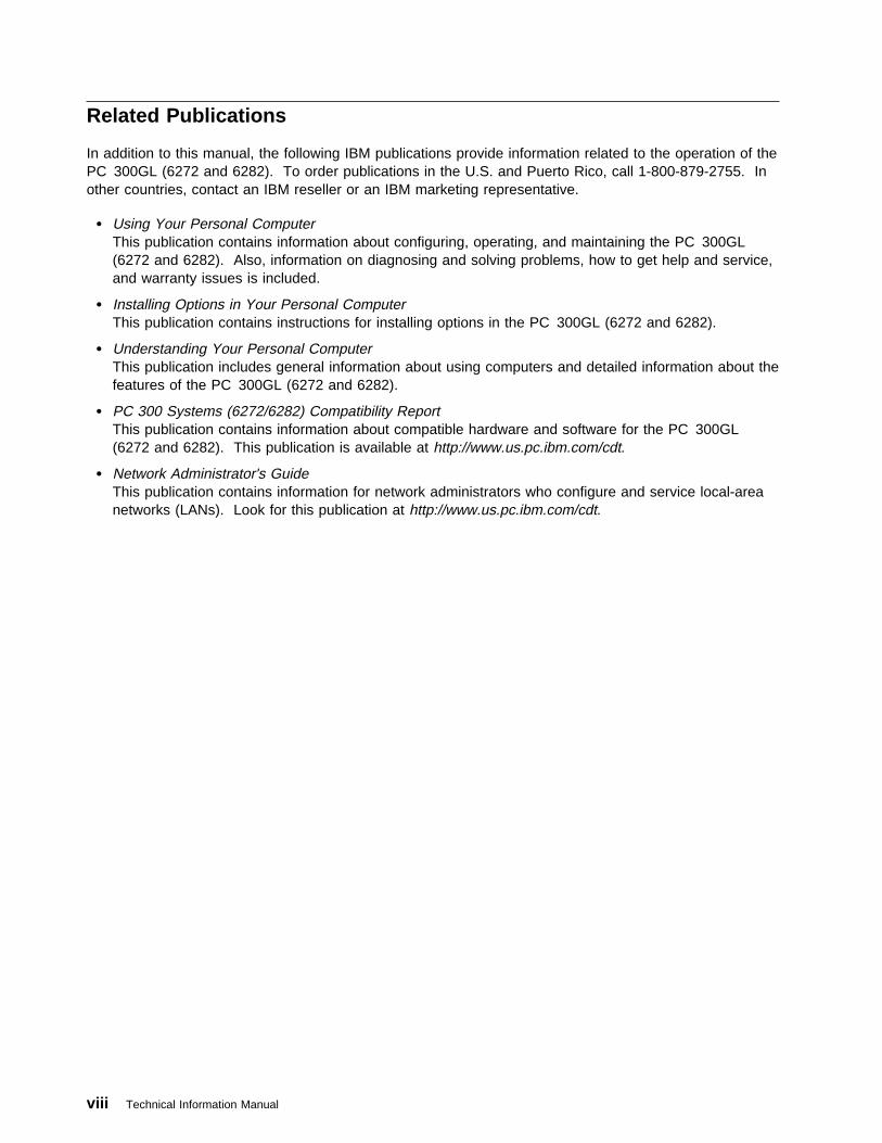
Related Publications
In addition to this manual, the following IBM publications provide information related to the operation of thePC 300GL (6272 and 6282). To order publications in the U.S. and Puerto Rico, call 1-800-879-2755. Inother countries, contact an IBM reseller or an IBM marketing representative.
� Using Your Personal ComputerThis publication contains information about configuring, operating, and maintaining the PC 300GL(6272 and 6282). Also, information on diagnosing and solving problems, how to get help and service,and warranty issues is included.
� Installing Options in Your Personal ComputerThis publication contains instructions for installing options in the PC 300GL (6272 and 6282).
� Understanding Your Personal ComputerThis publication includes general information about using computers and detailed information about thefeatures of the PC 300GL (6272 and 6282).
� PC 300 Systems (6272/6282) Compatibility ReportThis publication contains information about compatible hardware and software for the PC 300GL(6272 and 6282). This publication is available at http://www.us.pc.ibm.com/cdt.
� Network Administrator's GuideThis publication contains information for network administrators who configure and service local-areanetworks (LANs). Look for this publication at http://www.us.pc.ibm.com/cdt.
viii Technical Information Manual

Manual Style
Warning: The term reserved describes certain signals, bits, and registers that should not be changed.Use of reserved areas can cause compatibility problems, loss of data, or permanent damage to thehardware. When the contents of a register are changed, the state of the reserved bits must be preserved.When possible, read the register first and change only the bits that must be changed.
In this manual, some signals are represented in a small, all-capital-letter format (-ACK). A minus sign infront of the signal indicates that the signal is active low. No sign in front of the signal indicates that thesignal is active high.
The use of the letter “h” indicates a hexadecimal number. Also, when numerical modifiers such as “K”,“M” and “G“ are used, they typically indicate powers of 2, not powers of 10. For example, 1 KB equals1 024 bytes (2 10), 1 MB equals 1 048 576 bytes (2 20), and 1 GB equals 1 073 741 824 bytes (230).
When expressing storage capacity, MB equals 1 000 KB (1 024 000). The value is determined by countingthe number of sectors and assuming that every two sectors equals 1 KB.
Note: Depending on the operating system and other system requirements, the storage capacity availableto the user might vary.
Preface ix

x Technical Information Manual

Chapter 1. System Overview
Chapter 1. System Overview
The IBM PC 300GL (6272 and 6282) are versatile products designed to provide state-of-the-art computingpower with room for future growth. Several model variations are available.
Major Features
The major features are:
� Intel Pentium Processor or Intel Pentium Processor with MMX Technology
� 256 KB of external L2 cache (expandable to 512 KB)
� Up to 128 MB of system memory
� Cirrus CL-GD5446 video subsystem
� 1 MB of video memory expandable to 2 MB or 2 MB standard
� Industry-standard compatibility
� Network connection
– Integrated 10BASE-T Ethernet controller (some models only)– Ethernet Wake on LAN adapter (some models only)– Token-ring Wake on LAN adapter (some models only)
� ISA/PCI I/O-bus compatibility
� ISA/PCI expansion slots
� Enhanced IDE drives
� Bus master IDE controller
� Two 16550-UART serial ports
� Two USB ports
� One 15-pin monitor port
� One infrared port
� One parallel port
� Ports for keyboard and mouse
� Preinstalled 16X Max CD-ROM drive (some models only)
� Preinstalled SoundBlaster compatible audio adapter (some models only)
� EnergyStar compliant
� Choice of system unit size
– The PC 300GL 6272 has two expansion slots and three drive bays– The PC 300GL 6282 has four expansion slots and four drive bays
� PC 300GL 6272 Without Diskette Drive is shipped with a cover torx screw for extra security andwithout a diskette or CD-ROM drive
Copyright IBM Corp. October 1997 1

Chapter 1. System Overview
Other Features
The following features are supported by the PC 300GL (6272 and 6282). Optional hardware is requiredfor these features.
Wake on LAN
The power supply of the computer supports Wake on LAN. Wake on LAN allows the computer to turn onwhen a specific LAN frame is passed to the PC over the LAN.
To use Wake on LAN, the computer must be equipped with a network subsystem that also supports Wakeon LAN. The integrated Ethernet feature provided with some computers supports Wake on LAN. If IBMhas equipped your computer with an Ethernet or token ring adapter, it also supports Wake on LAN.
The menu used for setting the Wake on LAN feature is found in the Configuration/Setup Utility program.
Wake Up On RingAll models are configurable to turn on the computer after a ring is detected from an external or internalmodem. The menu used for setting the Wake Up On Ring feature is found in the Configuration/SetupUtility program. Two options control this feature:
� Serial Ring Detect: Use this option if the computer has an external modem connected to the serialport.
� Modem Ring Detect: Use this option if the computer has an internal modem.
Network Enablement
The PC 300GL (6272 and 6282) is enabled to support management over the network. The following is alist of functions that are supported:
� Selectable startup sequence� Selectable Automatic Power On Startup Sequence� Update POST/BIOS form network
� Ethernet setup� Wake on LAN� CMOS Save/Restore utility� CMOS setup over LAN
2 Technical Information Manual

Chapter 2. System Board Features
Chapter 2. System Board Features
This section includes information about system board features. For an illustration of the system board,see “System Board” on page 13.
Microprocessor
The microprocessor in the PC 300GL (6272 and 6282) is the Intel Pentium Processor or the Intel PentiumProcessor with MMX Technology. The microprocessor features are:
� Intel Pentium Processor
– 8 KB write-through code cache (internal)– 8 KB write-back data cache (internal)
� Intel Pentium Processor with MMX Technology
– 16 KB write-through code cache (internal)– 16 KB write-back data cache (internal)– Split power supplies (VIO = 3.3 V, VCORE = 2.8 V)– Support for Intel architecture MMX technology
� Superscalar architecture
� Branch prediction
� Power management capabilities
� Enhanced floating point capabilities
� 64-bit data bus, 32-bit address bus
The system board operates with a 3.3 volt microprocessor. The microprocessor plugs directly into a321-pin zero-insertion-force (ZIF) socket (Socket 7). Socket 7 allows for a performance upgrade. Afterinstalling an upgrade, the internal speed of the microprocessor is updated by setting switches on thesystem board. For information on switch configuration, see “Switches” on page 14.
Copyright IBM Corp. October 1997 3

Chapter 2. System Board Features
Chipset Control
The Intel Triton-VX chipset is the interface between the microprocessor and the following:
� L2 cache controller � Memory subsystem � PCI bus� Bus master IDE connection� High performance PCI to ISA bridge
� USB port
L2 Cache
The chipset supports an L2 cache that uses pipeline-burst, synchronous random access memory (SRAM).L2 cache modules are removable and the base size module of 256 KB is upgradeable to 512 KB. Inaddition to these sizes, a "cacheless" state with 0 KB of L2 cache is supported. Characteristics of eachL2 cache size are shown below.
The L2 cache is a look-aside, direct-mapped (one-way associativity) cache architecture. The L2 cacheoperates in write-back mode, and by default, is implemented as unified cache (stores code and data). TheL2 cache supports the cache timings shown below.
Figure 1. L2 Cache Characteristics
Cache Characteristics 256 KB L2 Cache 512 KB L2 Cache
Cacheable Memory 64 MB 64 MB
Line Size 32 bytes 32 bytes
SRAM Type 2 chips 32K x 32 4 chips 32K x 32
SRAM Voltage 3.3 V with 3.3 V output 3.3 V with 3.3 V output
SRAM Speed 8.5 ns 8.5 ns
Tag RAM Type 1 chip 8K x 8 2 chips 8K x 8 or 1 chip 16K x 8
Tag RAM Voltage 5 V 5 V
Tag RAM Speed 15 ns 15 ns
Tag RAM Tag Address A(25:18) A(25:19)
Tag RAM Set Address A(17:5) A(18:5)
Figure 2. L2 Cache Timings
Cycle 256 KB L2 (60/66 MHz) 512 KB L2 (60/66 MHz)
Single Read 3 3
Burst Read Hit 3-1-1-1 3-1-1-1
Burst Read Hit Pipelined 3-1-1-1-1-1-1-1 3-1-1-1-2-1-1-1
Single Write 3 3
Burst Write Hit 3-1-1-1 3-1-1-1
Write Miss NA NA
4 Technical Information Manual

Chapter 2. System Board Features
System Memory
The system memory interface is controlled by the chipset. Synchronous dynamic random access memory(SDRAM) is standard.
The maximum amount of system memory is 128 MB. For memory expansion, the system board providestwo dual inline memory module (DIMM) connectors. DIMM sizes of 8MB, 16MB, 32MB, and 64MB with aspeed of 60ns are supported. The amount of memory preinstalled varies by model.
The following information applies to system memory:
� SDRAM, nonparity memory is standard.� Extended data output (EDO), nonparity DRAM is also supported.� The maximum height of memory modules is 3.18 cm (1.25 in.).� Only industry-standard, gold-lead DIMMs are supported.� A mix of parity and nonparity types configures as nonparity.
For information on the pin assignments for the memory module connectors, see “System MemoryConnector” on page 32.
The following figure shows configuration information for the supported DIMMs.
Figure 3. System Memory Configuration
Total Memory (MB) DIMM 0 DIMM 1
8 8 0
16 8 8
16 16 0
24 16 8
24 8 16
32 32 0
32 16 16
40 8 32
48 16 32
64 32 32
72 8 64
80 16 64
96 32 64
128 64 64
Chapter 2. System Board Features 5

Chapter 2. System Board Features
PCI Bus
The fully synchronous 30/33 MHz PCI bus originates in the chipset. Features of the PCI bus are:
� Zero wait state microprocessor-to-PCI write interface for high performance graphics� Built-in PCI bus arbiter with support for up to five masters� Microprocessor-to-PCI memory write posting with 5 Dword deep buffers� Converts back-to-back sequential microprocessor-to-PCI memory write to PCI burst write� PCI-to-DRAM posting 18 Dwords� PCI-to-DRAM up to 120 MB/sec bandwidth� Multi-transaction timer to support multiple short PCI transactions within one PCI ARB cycle� PCI 2.1 compliant
Bus Master IDE Interface
The system board incorporates a PCI-to-IDE interface that complies with the AT Attachment Interface withExtensions. The subsystem that controls direct access storage devices (DASD) is integrated with the IDEinterface.
The chipset functions as a bus master for the IDE interface. The chipset is PCI 2.1 compliant; it connectsdirectly to the PCI bus and is designed to allow concurrent operations on the PCI bus and IDE bus. Thechipset is capable of supporting PIO mode 0-4 devices and IDE DMA mode 0-2 devices.
A ribbon cable provided with the computer can attach up to four IDE devices to the IDE connectors on thesystem board. The IDE devices receive their power through a four-position power cable containing +5,+12, and ground voltage. When adding devices to the IDE interface, one device is designated as theprimary or master device and another is designated as the secondary or subordinate device. Thesedesignations are determined by switches or jumpers on each device.
For the IDE interface, no resource assignments are given in the system memory or the direct memoryaccess (DMA) channels. For information on the resource assignments, see “Input/Output Address Map”on page 45 and Figure 52 on page 50 (for IRQ assignments).
Two connectors are provided on the system board for the IDE interface. For information on the connectorpin assignments, see “IDE Connectors” on page 34.
PCI to ISA Bridge
On the system board, the chipset provides the interface between the peripheral component interface (PCI)and industry standard architecture (ISA) buses. The chipset is used to convert PCI bus cycles to ISA buscycles; the chipset also includes all the subsystems of the ISA bus, including two cascaded interruptcontrollers, two DMA controllers with four 8-bit and three 16-bit channels, three counters equivalent to aprogrammable interval timer, and power management. The ISA bus operates at speeds of 7.5 MHz with a60 MHz microprocessor bus and 8.25 MHz with a 66 MHz microprocessor bus (one-quarter of the PCI busspeed).
For the ISA bus, no resource assignments are given in the system memory or the DMA channels. Forinformation on resource assignments, see “Input/Output Address Map” on page 45 and Figure 52 onpage 50 (for IRQ assignments).
6 Technical Information Manual

Chapter 2. System Board Features
USB Interface
Universal serial bus (USB) technology is a standard feature of the computer. Using the chipset, thesystem board provides the USB interface with two connectors. A USB-enabled device can attach to eachconnector, and if that device is a hub, multiple peripherals can attach to the hub and be used by thesystem. The USB connectors use Plug and Play technology for installed devices. The speed of the USBis up to 12 Mb/s with a maximum of 127 peripherals.
Features provided by USB technology include:
� Hot pluggable� Support for concurrent operation of multiple devices� Suitable for different device bandwidths� Up to five meters length from host to hub or hub to hub� Guaranteed bandwidth and low latencies appropriate for specific devices� Wide range of packet sizes� Limited power to hubs
For information on the connector pin assignments for the USB interface, see “USB Connectors” onpage 35.
Chapter 2. System Board Features 7

Chapter 2. System Board Features
Video Subsystem
The video subsystem on the system board includes the Cirrus CL-GD5446 chip and up to 2 MB of EDODRAM.
Cirrus CL-GD5446 Chip
The CL-GD5446 chip supports all video graphics array (VGA) modes and is compliant with super videographics array (SVGA) modes, Video Electronics Standards Association (VESA) 1.2. Some enhancedfeatures of the chip are:
� Plug and Play support� 50 nanosecond (ns) single-cycle EDO DRAM support� Advanced Power Management support� Color space conversion
� Hardware scaling
The chip is connected to the PCI bus and is PCI 2.1 compliant. The CL-GD5446 video subsystemsupports the VESA Display Data Channel (DDC) standard 1.1 and uses DDC1 and DDC2B to determineoptimal values during automatic monitor detection.
For information on resource assignments, see Appendix B, “System Address Maps” on page 44 andAppendix C, “IRQ and DMA Channel Assignments” on page 50.
The video subsystem provides a 15-pin monitor port on the system board; For information on connectorpin assignments, see “Monitor Connector” on page 35.
Video Memory
The video memory modules used are 256 KB x 16 (512 KB total) 50 nanosecond (ns) EDO DRAMs.
The maximum amount of video memory that can be used with the video subsystem is 2 MB. Systems areshipped standard with either two modules that total 1 MB and create a 32-bit data path to video memoryor four modules that total 2 MB and create a 64-bit data path to video memory. For systems with 1 MB ofvideo memory, an upgrade is available.
8 Technical Information Manual

Chapter 2. System Board Features
Input/Output Controller
Control of the integrated input/output (I/O) ports and diskette drive controller is provided by a single chip,the National Semiconductor PC87307. This chip, which supports Plug and Play, controls the followingfeatures:
� Diskette drive support � Serial port � Parallel port� Keyboard and mouse ports
� Infrared port� General purpose I/O ports
� Real-time clock� Advanced Power Management support
The chip requires an external 24 MHz frequency.
Diskette Drive Support
A maximum of two diskette drives and one tape backup drive is supported on the system board. Theactual number of diskette drives that can be installed is dependent upon the system unit size (thePC 300GL 6272 has three drive bays for installing devices and the PC 300GL 6282 has four drive baysfor installing internal devices). The following is a list of devices that the diskette drive subsystem supports:
� 1.44 MB, 3.5" diskette drive� 2.88 MB, 3.5" diskette drive� 1.2 MB, 5.25" diskette drive
One connector is provided on the system board for diskette drive support. For information on theconnector pin assignments, see “Diskette Drive Connector” on page 35.
Serial Port
Integrated into the system board are two universal asynchronous receiver/transmitter (UART) serial ports.The serial ports include a 16-byte data, first-in first-out (FIFO) buffer, and have programmable baud rategenerators. The serial ports are NS16450 and PC16550A compatible.
For information on the connector pin assignments, see “Serial Port Connectors” on page 37.
Note: Current loop interface is not supported.
The following figure shows the serial port assignments used in configuration.
Figure 4. Serial Port Assignments
Port Assignment Address Range IRQ Level
Serial 1 03F8h–03FFh IRQ4
Serial 2 02F8h–02FFh IRQ3
Serial 3 03E8h–03FFh IRQ4
Serial 4 02E8h–02FFh IRQ3
Chapter 2. System Board Features 9

Chapter 2. System Board Features
Parallel Port
Integrated in the system board is support for extended capabilities port (ECP), enhanced parallel port(EPP) and standard parallel port (SPP) modes. The modes of operation are selected through theConfiguration/Setup Utility program with the default mode set to SPP.
The following figure shows the parallel port assignments used in configuration.
The system board has one connector for the parallel port. For information on the connector pinassignments, see “Parallel Port Connector” on page 37.
Keyboard and Mouse Ports
The keyboard and mouse subsystem is controlled by a general purpose 8-bit microcontroller; it iscompatible with 8042AH. The controller consists of 256 bytes of data memory and 2 KB of read onlymemory (ROM).
The controller has two logical devices: one controls the keyboard and the other controls the mouse. Thekeyboard has two fixed I/O addresses and a fixed IRQ line and can operate without the mouse. Themouse cannot operate without the keyboard because, although it has a fixed IRQ line, the mouse relies onthe addresses of the keyboard for operation. For the keyboard and mouse interfaces, no resourceassignments are given in the system memory addresses or DMA channels. For information on theresource assignments, see “Input/Output Address Map” on page 45 and Figure 52 on page 50 (for IRQassignments).
The system board has one connector for the keyboard port and one connector for the mouse port. Forinformation on the connector pin assignments, see “Keyboard and Mouse Port Connectors” on page 38.
Figure 5. Parallel Port Assignments
Port Assignment Address Range IRQ Level
Parallel 1 03BCh–03BEh IRQ7
Parallel 2 0378h–037Fh IRQ5
Parallel 3 0278h–027Fh IRQ5
10 Technical Information Manual
Chapter 2. System Board Features
Network Connection
Some models have a Crystal CS8920 Ethernet 10BASE-T controller and an RJ-45 connector integrated onthe system board that provides a high-performance LAN connection. This integrated Ethernet is an ISAPlug and Play device with built-in support for Wake on LAN.
Some models are equipped with an Ethernet or token-ring adapter.
Features of the Ethernet adapter are:
� Operation in shared 10BASE-T or 100BASE-TX environment� Transmits and receives data at 10 Mbps or 100 Mbps� RJ-45 connector for LAN attachment� Operates in symmetrical multiprocessing (SMP) environments� Wake on LAN support� Remote Program Load (RPL) support
Note: The following information is for PC 300GL 6272 Without Diskette Drive computers:
For operation of the computer within FCC Class A limits, you must use category 5 network cablingat 10 Mbps or 100 Mbps.
Features of the token-ring adapter are:
� Transmits and receives data at 4 Mbps or 16 Mbps� RJ-45 and D-shell connectors for LAN attachment� Wake on LAN support� Remote Program Load (RPL) support
General Purpose I/O Ports
The system board has up to 16 general purpose input/output (GPIO) pins which are implemented by two8-bit GPIO ports. The use of GPIO pins is dependent upon system design. Features of the GPIO portsare:
� Open-drain outputs with internal pull-ups and transistor-transistor logic (TTL) inputs� Base address is software configurable� Direction is programmable� Occupies 4-byte I/O address
Real-Time Clock and CMOS
The real-time clock is a low-power clock that provides a time-of-day clock and a calendar. The clocksettings are maintained by an external battery source of 3 V.
The system uses 242 bytes of memory to store complementary metal-oxide semiconductor (CMOS)memory. Moving a jumper (J6) on the system board erases CMOS memory.
To locate the battery or J18, see “System Board” on page 13.
Chapter 2. System Board Features 11

Chapter 2. System Board Features
Flash EEPROM
The system board uses a flash electrically-erasable, programmable, read-only memory (EEPROM) chip tostore the basic input/output system (BIOS), video BIOS, IBM logo, Configuration/Setup Utility, and Plugand Play data.
If necessary, the EEPROM can be easily updated using a standalone utility program that is available on a3.5" diskette.
Riser Card
The system board uses a riser card to route PCI and ISA bus signals to the expansion connectors. EachISA-expansion connector is 16-bits, and each PCI-expansion connector is 32-bits. PCI-expansionconnectors support the 32-bit 5-V dc local-bus signalling environment that is defined in PCI Local BusSpecification 2.1. The ISA bus is buffered to provide sufficient drive for the ISA-expansion connectors,assuming two low-power Schottky (LS) loads per slot.
The system board uses one of two riser cards. Different riser cards provide a different configuration ofPCI and ISA connectors and are representative of the different mechanical sizes. The following figuresummarizes the characteristics of the two riser cards.
For information on the connector pin assignments, see “ISA Connectors” on page 39 and “PCI Connector”on page 41.
Figure 6. Riser Card Characteristics
Expansion Slots 2x3 Riser Card 4x4 Riser Card
Shared ISA/PCI 2 2
Dedicated ISA 0 1
Dedicated PCI 0 1
12 Technical Information Manual

Chapter 2. System Board Features
Physical Layout
The system board might look slightly different from the one shown.
Note: A diagram of the system board, including switch and jumper settings, is attached to the undersideof the computer cover.
System Board.1/ Monitor port.2/ Parallel port.3/ Universal Serial Bus Port.4/ Universal Serial Bus Port.5/ Mouse port.6/ Keyboard port.7/ Serial port 1.8/ Ethernet port (some models only).9/ Serial port 2 connector.1ð/ Main power connector (J2).11/ Clear CMOS jumper (J6).12/ Diskette drive connector (J3).13/ Primary IDE connector (J12).14/ Secondary IDE connector (J13).15/ Power LED connector (J8).16/ DIMM sockets (J14 and J16).17/ Configuration switch (SW1).18/ 3.3 V power connector (J22).19/ Fan connector (J18).2ð/ LAN activity LED connector (J24) (some models only).21/ COAST cache module socket (J26).22/ Pentium processor socket 7.23/ Riser connector.24/ Battery.25/ Video RAM expansion sockets (U20 and U25).26/ Wake on LAN connector (J28).27/ Wakeup on Modem/Ring connector (J27)
Chapter 2. System Board Features 13

Chapter 2. System Board Features
Jumpers
Jumpers on the system board are used for custom configurations. The following figures show thedescription of pin numbers for specific jumpers. To locate these jumpers, see “System Board” onpage 13.
Switches
The switches (SW1) are used for setting the microprocessor speed and diskette-write protection.
The following figure shows the configuration of switches 1–4 for the different microprocessor speeds.
The following figure shows the configuration of switch 5 for disabling or enabling the Ethernet controller.
Note: This switch is functional only on models with integrated/on-board Ethernet only.
Note: This switch should not be used to disable the Ethernet controller under normal conditions. BIOSwill disable it if selected in setup. This switch should only be used to aid in diagnosing problems.
The following figure shows the configuration of switch 6 for diskette-write protection.
Figure 7. J6 CMOS Clear/Password Jumper
Pins Description
1 and 2 Normal
2 and 3 Clear CMOS/Password
Figure 8. Microprocessor Speed (SW1 1-4)
Switch 100 MHz 120 MHz 133 MHz 150 MHz 166 MHz 200 MHz 233 MHz
1 Off On On On On Off Off
2 Off Off Off On On On Off
3 Off On Off On Off Off Off
4 On Off On Off On On On
Figure 9. Ethernet Disable/Enable (SW1 5)
Switch Enabled Disabled
5 On Off
Figure 10. Diskette-Write Protection (SW1 6)
Switch Diskette Write-Enabled Diskette Write-Protected
6 Off On
14 Technical Information Manual

Chapter 2. System Board Features
Connectivity
The connections the computer provides are at the back of the computer. The connectors are:
� Network
– Ethernet integrated with the system board (some models only)– Ethernet or token ring adapter (some models only)
� Keyboard
� Mouse
� Serial (2)
� Parallel
� Monitor
� USB (2)
� Audio (some models only)
Connections integrated with the system board can be identified by a symbol directly above the connection.Connectors provided by an adapter might not have an identifying symbol, as shown in the followingillustration.
MonitorKeyboard
MouseSerial USB ParallelEthernet
(Audio Adapter)
Serial
B
1 2A
Game/MIDI MicrophoneLine In
Line Out
The following illustration shows the connections for the PC 300GL 6272 Without Diskette Drive.
MonitorKeyboard
MouseSerial USB Parallel
AudioAdapter
NetworkAdapter
Serial
B
1 2A
MicrophoneMIDI/Game
SpeakersLineIn
LineOut
Note: Connections can vary by computer.
Chapter 2. System Board Features 15

Chapter 3. Physical Specifications
Chapter 3. Physical Specifications
This section lists the physical specifications for the PC 300GL (6272 and 6282). The PC 300GL 6272has two expansion slots and three drive bays, and the PC 300GL 6282 has four expansion slots and fourdrive bays.
Note:
� The maximum altitude for the PC 300GL (6272 and 6282) is 2133.6 m (7000 ft.). This is themaximum altitude at which the specified air temperatures apply. At higher altitudes, themaximum air temperatures are lower than those specified.
� The PC 300GL (6272 and 6282) computers are electromagnetic compatible with FCC Class B.
� The PC 300GL 6272 Without Diskette Drive computers are electromagnetic compatible withFCC Class A.
16 Copyright IBM Corp. October 1997

Chapter 3. Physical Specifications
PC 300GL 6272
The following figures list the physical attributes for the PC 300GL 6272.
Figure 11. Size (PC 300GL 6272)
Description Measurement
Width 369 mm (14.5 in)
Depth 400 mm (15.8 in)
Height 95 mm (3.7 in)
Figure 12. Weight (PC 300GL 6272)
Description Measurement
Minimum configuration 6.8 kg (15.0 lb)
Maximum configuration (fully populated with typical options) 10.4 kg (23.0 lb)
Figure 13. Cables (PC 300GL 6272)
Description Measurement
Power cable 1.8 m (6 ft)
Keyboard cable 2 m (6 ft 6.7 in)
Figure 14. Air Temperature (PC 300GL 6272)
Description Measurement
System on 10.0 to 32.0°C (50 to 90°F)
System off 10.0 to 43.0°C (50 to 110°F)
Chapter 3. Physical Specifications 17

Chapter 3. Physical Specifications
Figure 15. Humidity (PC 300GL 6272)
Description Measurement
System on 8% to 80%
System off 8% to 80%
Figure 16. Heat Output (PC 300GL 6272)
Description Measurement
Minimum configuration 35 W (120 Btu per hour)
Maximum configuration (based on 145-watt maximum capacity of the power supply) 200 W (685 Btu per hour)
Figure 17. Electrical (PC 300GL 6272)
Description Measurement
Low range 90 (min) to 137 (max) V ac
High range 180 (min) to 265 (max) V ac
Frequency 50 ± 3 Hz or 60 ± 3 Hz
Input, Minimum configuration 0.08 kVA
Input, Maximum configuration 0.30 kVA
18 Technical Information Manual
Chapter 3. Physical Specifications
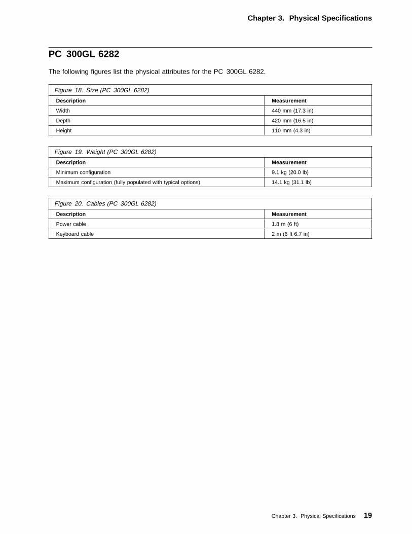
PC 300GL 6282
The following figures list the physical attributes for the PC 300GL 6282.
Figure 18. Size (PC 300GL 6282)
Description Measurement
Width 440 mm (17.3 in)
Depth 420 mm (16.5 in)
Height 110 mm (4.3 in)
Figure 19. Weight (PC 300GL 6282)
Description Measurement
Minimum configuration 9.1 kg (20.0 lb)
Maximum configuration (fully populated with typical options) 14.1 kg (31.1 lb)
Figure 20. Cables (PC 300GL 6282)
Description Measurement
Power cable 1.8 m (6 ft)
Keyboard cable 2 m (6 ft 6.7 in)
Chapter 3. Physical Specifications 19
Chapter 3. Physical Specifications
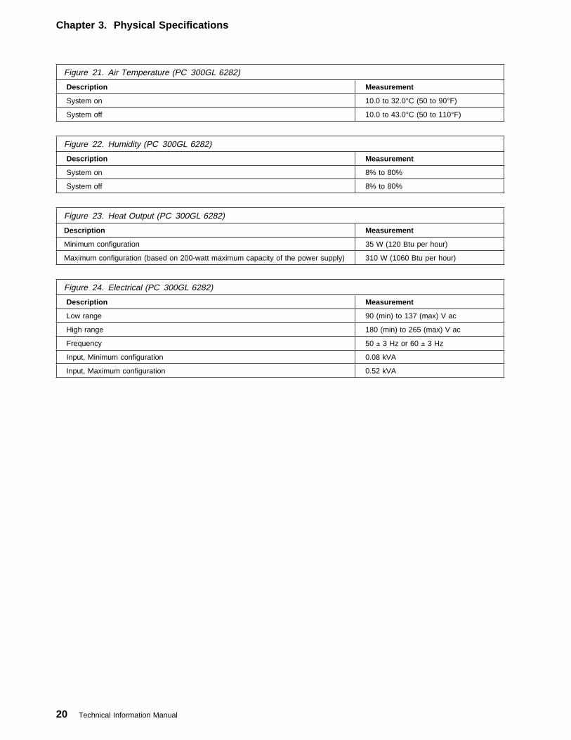
Figure 21. Air Temperature (PC 300GL 6282)
Description Measurement
System on 10.0 to 32.0°C (50 to 90°F)
System off 10.0 to 43.0°C (50 to 110°F)
Figure 22. Humidity (PC 300GL 6282)
Description Measurement
System on 8% to 80%
System off 8% to 80%
Figure 23. Heat Output (PC 300GL 6282)
Description Measurement
Minimum configuration 35 W (120 Btu per hour)
Maximum configuration (based on 200-watt maximum capacity of the power supply) 310 W (1060 Btu per hour)
Figure 24. Electrical (PC 300GL 6282)
Description Measurement
Low range 90 (min) to 137 (max) V ac
High range 180 (min) to 265 (max) V ac
Frequency 50 ± 3 Hz or 60 ± 3 Hz
Input, Minimum configuration 0.08 kVA
Input, Maximum configuration 0.52 kVA
20 Technical Information Manual

Chapter 4. Power Supply
Chapter 4. Power Supply
The power supply requirements are supplied by a 85-watt (PC 300GL 6272) or 145-watt (PC 300GL6282) power supply. The power supply converts the ac input voltage into four dc output voltages andprovides power for the following:
� System board � Adapters� Internal DASD drives� Keyboard and auxiliary devices
A logic signal on the power connector controls the power supply; the front panel switch is not directlyconnected to the power supply.
Power Input
The following figure shows the input power specifications. The power supply has a manual switch toselect the correct input voltage.
Figure 25. Power Input Requirements
Specification Measurements
Input voltage, low range 90 (min)–137 (max) V ac
Input voltage, high range 180 (min)–265 (max) V ac
Input frequency 50 Hz ± 3 Hz or 60 Hz ± 3 Hz
Copyright IBM Corp. October 1997 21

Chapter 4. Power Supply
Power Output
The power supply outputs shown in the following figures include the current supply capability of all theconnectors, including system board, DASD, PCI, and auxiliary outputs.
Note: Simultaneous loading of +5 V and +3.52 V must not exceed 50 watts.
PC 300GL 6272
PC 300GL 6282
Figure 26. Power Output (85 Watt)
Output Voltage Regulation Minimum Current Maximum Current
+5 volts +5% to -4% 1.0 A 10.0 A
+12 volts +5% to -5% 0.2 A 2.5 A
-12 volts +10% to -9% 0.0 A 0.4 A
-5 volts +10% to -10% 0.0 A 0.3 A
+3.52 volts +2% to -2% 0.0 A 7.0 A
+5 volt (auxiliary) +5% to -10% 0.0 A .02 A
+5 volt (LAN Wake-Up) +5% to -10% 0.0 A .25 A
Figure 27. Power Output (145 Watt)
Output Voltage Regulation Minimum Current Maximum Current
+5 volts +5% to -4% 1.5 A 18.0 A
+12 volts +5% to -5% 0.2 A 4.2 A
-12 volts +10% to -9% 0.0 A 0.4 A
-5 volts +10% to -10% 0.0 A 0.3 A
+3.52 volts +2% to -2% 0.0 A 10.0 A
+5 volt (auxiliary) +5% to -10% 0.0 A .02 A
+5 volt (Wake on LAN) +5% to -10% 0.0 A .50 A
22 Technical Information Manual

Chapter 4. Power Supply
Component Outputs
The power supply provides separate voltage sources for the system board and internal storage devices.The following figures show the approximate power that is provided for specific system components. Manycomponents draw less current than the maximum shown.
Note: For each PCI connector, the maximum power consumption is rated at 25 watts for +5 V and+3.52 V combined.
Figure 28. System Board
Supply Voltage Maximum Current Regulation Limits
+3.52 V dc 3000 mA +2% to −2.0%
+5.0 V dc 4000 mA +5.0% to −4.0%
+12.0 V dc 25.0 mA +5.0% to −5.0%
−12.0 V dc 25.0 mA +10.0% to −9.0%
Figure 29. Keyboard Port
Supply Voltage Maximum Current Regulation Limits
+5.0 V dc 275 mA +5.0% to −4.0%
Figure 30. Auxiliary Device Port
Supply Voltage Maximum Current Regulation Limits
+5.0 V dc 300 mA +5.0% to −4.0%
Figure 31. ISA-Bus Adapters (Per Slot)
Supply Voltage Maximum Current Regulation Limits
+5.0 V dc 4500 mA +5.0% to −4.0%
−5.0 V dc 200 mA +5.0% to −5.0%
+12.0 V dc 1500 mA +5.0% to −5.0%
−12.0 V dc 300 mA +10.0% to −9.0%
Figure 32. PCI-Bus Adapters (Per Slot)
Supply Voltage Maximum Current Regulation Limits
+5.0 V dc 5000 mA +5.0% to −4.0%
+3.52 V dc 5000 mA +5.0% to −4.0%
Chapter 4. Power Supply 23
Chapter 4. Power Supply
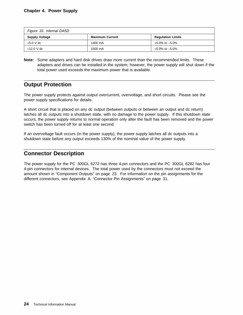
Note: Some adapters and hard disk drives draw more current than the recommended limits. Theseadapters and drives can be installed in the system; however, the power supply will shut down if thetotal power used exceeds the maximum power that is available.
Output Protection
The power supply protects against output overcurrent, overvoltage, and short circuits. Please see thepower supply specifications for details.
A short circuit that is placed on any dc output (between outputs or between an output and dc return)latches all dc outputs into a shutdown state, with no damage to the power supply. If this shutdown stateoccurs, the power supply returns to normal operation only after the fault has been removed and the powerswitch has been turned off for at least one second.
If an overvoltage fault occurs (in the power supply), the power supply latches all dc outputs into ashutdown state before any output exceeds 130% of the nominal value of the power supply.
Connector Description
The power supply for the PC 300GL 6272 has three 4-pin connectors and the PC 300GL 6282 has four4-pin connectors for internal devices. The total power used by the connectors must not exceed theamount shown in “Component Outputs” on page 23. For information on the pin assignments for thedifferent connectors, see Appendix A, “Connector Pin Assignments” on page 31.
Figure 33. Internal DASD
Supply Voltage Maximum Current Regulation Limits
+5.0 V dc 1400 mA +5.0% to −5.0%
+12.0 V dc 1500 mA +5.0% to −5.0%
24 Technical Information Manual

Chapter 5. System Software
Chapter 5. System Software
This section briefly describes some of the system software included with the computer.
BIOS
The system uses the IBM SurePath basic input/output system (BIOS), which is stored in flash electricallyerasable programmable read only memory (EEPROM). Some features of the BIOS are:
� PCI support according to PCI BIOS Specification 2.1� Plug and Play support according to Plug and Play BIOS Specification 1.1� Advanced Power Management (APM) support according to APM BIOS Interface Specification 1.2� PCI Bus Master IDE interface with device specific performance tuning� IDE LBA support� Cirrus video BIOS for the video chip� Bootable CD-ROM support� Flash over LAN support
Plug and Play
Support for Plug and Play conforms to the following:
� Plug and Play BIOS Specification 1.1 and 1.0� Plug and Play BIOS Extension Design Guide 1.0� Plug and Play BIOS Specification, Errata and Clarifications 1.0� Guide to Integrating the Plug and Play BIOS Extensions with system BIOS 1.2� Plug and Play Kit for DOS and Windows
POST
IBM power-on self test (POST) code is used. Also, initialization code is included for the Intel 54Cmicroprocessor, the National PC87307 chip, the I/O chip, and the Cirrus video chip.
POST error codes include text messages for determining the cause of an error. For more information, seeAppendix D, “Error Codes” on page 52.
Configuration/Setup Utility
The Configuration/Setup Utility program provides menus for selecting options for devices, I/O ports, dateand time, system security, start options, advanced setup, ISA legacy resources, and power management.
More information on using the Configuration/Setup Utility program is provided in Using Your PersonalComputer.
Copyright IBM Corp. October 1997 25

Chapter 5. System Software
Advanced Power Management (APM)
The PC 300GL (6272 and 6282) come with built-in energy-saving capabilities. Advanced PowerManagement (APM) is a feature that reduces the power consumption of systems when they are not beingused. When enabled, APM initiates reduced-power modes for the monitor, microprocessor, and hard diskdrive after a specified period of inactivity.
The BIOS supports APM 1.1. This enables the system to enter a power managed state, which reducesthe power drawn from the ac wall outlet. Advanced Power Management is enabled through theConfiguration/Setup Utility program and is controlled by the individual operating system.
For more information on APM, see Using Your Personal Computer and Understanding Your PersonalComputer.
Flash Update Utility
The flash update utility is a standalone program to support flash code updates. This utility programupdates the BIOS code in flash and the MRI to different languages.
The flash update utility program is available on a 3.5" diskette.
Diagnostic Programs
Two diagnostic products are supplied with the PC 300GL (6272 and 6282): QAPlus/WIN-WIN, a Windowsprogram which provides the best software coverage, and QAPlus/PRO for DOS which provides the besthardware coverage. For more information on these diagnostic programs, see Using Your PersonalComputer.
PC 300GL 6272 Without Diskette Drive computers use the PC Doctor programs and IBM advanceddiagnostics. See About Your Software and Using Your Personal Computer for more information.
26 Technical Information Manual
Chapter 6. System Compatibility
Chapter 6. System Compatibility
This chapter discusses some of the hardware, software, and BIOS compatibility issues for the computer.Refer to PC 300 Systems (6272/6282) Compatibility Report for a list of compatible hardware and softwareoptions.
Hardware Compatibility
This section discusses hardware, software, and BIOS compatibility issues that must be considered whendesigning application programs.
Many of the interfaces are the same as those used by the IBM Personal Computer AT. In most cases,the command and status organization of these interfaces is maintained.
The functional interfaces are compatible with the following interfaces:
� The Intel 8259 interrupt controllers (edge-triggered mode)
� The National Semiconductor NS16450 and NS16550A serial communication controllers
� The Motorola MC146818 Time of Day Clock command and status (CMOS reorganized)
� The Intel 8254 timer, driven from a 1.193 MHz clock (channels 0, 1, and 2)
� The Intel 8237 DMA controller, except for the Command and Request registers and the Rotate andMask functions; the Mode register is partially supported
� The Intel 8272 or 82077 diskette drive controllers
� The Intel 8042 keyboard controller at addresses 0060h and 0064h
� All video standards using VGA, EGA, CGA, MDA, and Hercules modes
� The parallel printer ports (Parallel 1, Parallel 2, and Parallel 3) in compatibility mode
Use the following information to develop application programs. Whenever possible, use the BIOS as aninterface to hardware to provide maximum compatibility and portability of applications among systems.
Copyright IBM Corp. October 1997 27

Chapter 6. System Compatibility
Hardware Interrupts
Hardware interrupts are level sensitive for PCI interrupts and edge sensitive for ISA interrupts. Theinterrupt controller clears its in-service register bit when the interrupt routine sends an End-of-Interrupt(EOI) command to the controller. The EOI command is sent regardless of whether the incoming interruptrequest to the controller is active or inactive.
The interrupt-in-progress latch is readable at an I/O-address bit position. This latch is read during theinterrupt service routine and might be reset by the read operation or it might require an explicit reset.
Note: For performance and latency considerations, designers might want to limit the number of devicessharing an interrupt level.
With level-sensitive interrupts, the interrupt controller requires that the interrupt request be inactive at thetime the EOI command is sent; otherwise, a new interrupt request will be detected. To avoid this, alevel-sensitive interrupt handler must clear the interrupt condition (usually by a read or write operation toan I/O port on the device causing the interrupt). After processing the interrupt, the interrupt handler:
1. Clears the interrupt
2. Waits one I/O delay
3. Sends the EOI
4. Waits one I/O delay
5. Enables the interrupt through the Set Interrupt Enable Flag command
Hardware interrupt IRQ9 is defined as the replacement interrupt level for the cascade level IRQ2.Program interrupt sharing is implemented on IRQ2, interrupt 0Ah. The following processing occurs tomaintain compatibility with the IRQ2 used by IBM Personal Computer products:
1. A device drives the interrupt request active on IRQ2 of the channel.
2. This interrupt request is mapped in hardware to IRQ9 input on the second interrupt controller.
3. When the interrupt occurs, the system microprocessor passes control to the IRQ9 (interrupt 71h)interrupt handler.
4. This interrupt handler performs an EOI command to the second interrupt controller and passes controlto the IRQ2 (interrupt 0Ah) interrupt handler.
5. This IRQ2 interrupt handler, when handling the interrupt, causes the device to reset the interruptrequest before performing an EOI command to the master interrupt controller that finishes servicingthe IRQ2 request.
28 Technical Information Manual

Chapter 6. System Compatibility
Diskette Drives and Controller
The following figures show the reading, writing, and formatting capabilities of each type of diskette drive.
Notes:
1. Do not use 5.25-inch diskettes that are designed for the 1.2MB mode in either a 250/500 KB or300/500 KB diskette drive.
2. Low-density 5.25-inch diskettes that are written to or formatted by a high-capacity 1.2 MB diskettedrive can be reliably read only by another 1.2 MB diskette drive.
3. Do not use 3.5-inch diskettes that are designed for the 2.88 MB mode in a 1.44MB diskette drive.
Copy Protection
The following methods of copy protection might not work in systems using the 3.5-inch 1.44 MB diskettedrive.
� Bypassing BIOS routines:
– Data transfer rate: BIOS selects the proper data transfer rate for the media being used.
– Diskette parameter table: Copy protection, which creates its own diskette parameter table, mightnot work in these drives.
� Diskette drive controls:
– Rotational speed: The time between two events in a diskette drive is a function of the controller.
– Access time: Diskette BIOS routines must set the track-to-track access time for the different typesof media that are used in the drives.
– ‘Diskette change’ signal: Copy protection might not be able to reset this signal.
� Write-current control: Copy protection that uses write-current control does not work, because thecontroller selects the proper write current for the media that is being used.
Hard Disk Drives and Controller
Reading from and writing to the hard disk is initiated in the same way as in IBM Personal Computerproducts; however, new functions are supported.
Figure 34. 5.25-Inch Diskette Drive Reading, Writing, and Formatting Capabilities
Diskette Drive Type 250/500 KB Mode 300/500 KB Mode 1 MB Mode
Single sided (48 TPI) RWF — —
Double sided (48 TPI) RWF RWF —
High capacity (1.2 MB) RWF RWF RWF
Figure 35. 3.5-Inch Diskette Drive Reading, Writing, and Formatting Capabilities
Diskette Drive Type 720 KB Mode 1.44 MB Mode 2.88 MB Mode
1.44 MB drive RWF RWF —
2.88 MB drive RWF RWF RWF
Chapter 6. System Compatibility 29

Chapter 6. System Compatibility
Software Compatibility
To maintain software compatibility, the interrupt polling mechanism that is used by IBM Personal Computerproducts is retained. Software that interfaces with the reset port for the IBM Personal Computerpositive-edge interrupt sharing (hex address 02Fx or 06Fx, where x is the interrupt level) does not createinterference.
Software Interrupts
With the advent of software interrupt sharing, software interrupt routines must daisy chain interrupts. Eachroutine must check the function value, and if it is not in the range of function calls for that routine, it musttransfer control to the next routine in the chain. Because software interrupts are initially pointed toaddress 0:0 before daisy chaining, check for this case. If the next routine is pointed to address 0:0 andthe function call is out of range, the appropriate action is to set the carry flag and do a RET 2 to indicatean error condition.
Machine-Sensitive Programs
Programs can select machine-specific features, but they must first identify the machine and model type.IBM has defined methods for uniquely determining the specific machine type. The machine model bytecan be found through Interrupt 15H, Return System Configuration Parameters function ((AH)=C0H).
30 Technical Information Manual
Appendix A. Connector Pin Assignments
Appendix A. Connector Pin Assignments
The following figures show the pin assignments for various system board connectors.
Copyright IBM Corp. October 1997 31

Appendix A. Connector Pin Assignments
System Memory Connector
1
85
84
168
Figure 36 (Page 1 of 3). System Memory Connector Pin Assignments
Pin Signal I/O Pin Signal I/O
1 GND NA 85 GND NA
2 MD0 I/O 86 MD32 I/O
3 MD1 I/O 87 MD33 I/O
4 MD2 I/O 88 MD34 I/O
5 MD3 I/O 89 MD35 I/O
6 VDD I/O 90 VDD NA
7 MD4 I/O 91 MD36 NA
8 MD5 I/O 92 MD37 I/O
9 MD6 I/O 93 MD38 I/O
10 MD7 I/O 94 MD39 I/O
11 PAR0 I/O 95 PAR4 I/O
12 GND NA 96 GND NA
13 MD16 I/O 97 MD48 I/O
14 MD17 I/O 98 MD49 I/O
15 MD18 I/O 99 MD50 I/O
16 MD19 I/O 100 MD51 I/O
17 MD20 I/O 101 MD52 I/O
18 VDD NA 102 VDD NA
19 MD21 I/O 103 MD53 I/O
20 MD22 I/O 104 MD54 I/O
21 MD23 I/O 105 MD55 I/O
22 PAR2 I/O 106 PAR6 I/O
23 GND I/O 107 GND NA
24 NC NA 108 NC NA
25 NC NA 109 NC NA
26 VDD NA 110 VDD NA
27 WE0 I 111 NC NA
28 CAS0 I 112 CAS2 I
29 CAS2 I 113 CAS3 I
30 RAS0 I 114 RAS1 I
31 OE0 I 115 NC NA
32 GND NA 116 GND NA
33 A0A I 117 A1 I
34 A2 I 118 A3 I
35 A4 I 119 A5 I
36 A6 I 120 A7 I
32 Technical Information Manual

Appendix A. Connector Pin Assignments
Figure 36 (Page 2 of 3). System Memory Connector Pin Assignments
Pin Signal I/O Pin Signal I/O
37 A8 I 121 A9 I
38 A10 I 122 A11 I
39 A12 I 123 A13 I
40 VDD NA 124 VDD NA
41 NC NA 125 NC NA
42 NC NA 126 B0 O
43 GND NA 127 GND NA
44 OE1 I 128 NC NA
45 RAS2 I 129 RAS3 I
46 CAS4 I 130 CAS6 I
47 CAS5 I 131 CAS7 I
48 WE1 I 132 PDE I
49 VDD NA 133 VDD NA
50 NC NA 134 NC NA
51 NC NA 135 NC NA
52 MD8 I/O 136 MD40 I/O
53 MD9 I/O 137 MD41 I/O
54 GND NA 138 GND NA
55 MD10 I/O 139 MD42 I/O
56 MD11 I/O 140 MD43 I/O
57 MD12 I/O 141 MD44 I/O
58 MD13 I/O 142 MD45 I/O
59 VDD NA 143 VDD NA
60 MD14 I/O 144 MD46 I/O
61 NC NA 145 NC NA
62 DU NA 146 NC NA
63 NC NA 147 NC NA
64 NC NA 148 GND NA
65 MD15 I/O 149 MD47 I/O
66 PAR1 I/O 150 PAR5 I/O
67 MD24 I/O 151 MD56 I/O
68 GND NA 152 GND NA
69 MD25 I/O 153 MD57 I/O
70 MD26 I/O 154 MD58 I/O
71 MD27 I/O 155 MD59 I/O
72 MD28 I/O 156 MD60 I/O
73 VDD NA 157 VDD NA
74 MD29 I/O 158 MD61 I/O
75 MD30 I/O 159 MD62 I/O
76 MD31 I/O 160 MD63 I/O
77 PAR3 I/O 161 PAR7 I/O
78 GND NA 162 GND NA
79 PD1 O 163 PD2 O
Appendix A. Connector Pin Assignments 33

Appendix A. Connector Pin Assignments
IDE Connectors
1
2 40
39
Figure 36 (Page 3 of 3). System Memory Connector Pin Assignments
Pin Signal I/O Pin Signal I/O
80 PD3 O 164 PD4 O
81 PD5 O 165 PD6 O
82 PD7 O 166 PD8 O
83 ID0 O 167 ID1 O
84 VDD NA 168 VDD NA
Figure 37. IDE Connector Pin Assignments
Pin Signal I/O Pin Signal I/O
1 RESET O 21 NC NA
2 Ground NA 22 Ground NA
3 Data bus bit 7 I/O 23 IO Write O
4 Data bus bit 8 I/O 24 Ground NA
5 Data bus bit 6 I/O 25 IO Read O
6 Data bus bit 9 I/O 26 Ground NA
7 Data bus bit 5 I/O 27 IO Channel Ready I
8 Data bus bit 10 I/O 28 ALE O
9 Data bus bit 4 I/O 29 NC NA
10 Data bus bit 11 I/O 30 Ground NA
11 Data bus bit 3 I/O 31 IRQ I
12 Data bus bit 12 I/O 32 CS16# I
13 Data bus bit 2 I/O 33 SA1 O
14 Data bus bit 13 I/O 34 PDIAG# I
15 Data bus bit 1 I/O 35 SA0 O
16 Data bus bit 14 I/O 36 SA2 O
17 Data bus bit 0 I/O 37 CS0# O
18 Data bus bit 15 I/O 38 CS1 O
19 Ground NA 39 Active# I
20 Key (Reserved) NA 40 Ground NA
34 Technical Information Manual

Appendix A. Connector Pin Assignments
USB Connectors
43
21
Monitor Connector
5 1
10 6
15 11
Diskette Drive Connector
Figure 38. USB Connector Pin Assignments
Pin Signal
1 VCC
2 -Data
3 +Data
4 Ground
Figure 39. Monitor Connector Pin Assignments
Pin Signal I/O Pin Signal I/O
1 Red O 2 Green O
3 Blue O 4 Monitor ID 2 - Notused
I
5 Ground NA 6 Red ground NA
7 Green ground NA 8 Blue ground NA
9 +5 V, used by DDC2B NA 10 Ground NA
11 Monitor ID 0 - Notused
I 12 DDC2B serial data I/O
13 Horizontal sync O 14 Vertical sync O
15 DDC2B clock I/O
Figure 40 (Page 1 of 2). Diskette Drive Connector Pin Assignments
Pin Signal I/O Pin Signal I/O
1 Drive 2 installed # I 2 High density select O
3 Not connected NA 4 Not connected NA
5 Ground NA 6 Data rate 0 NA
7 Ground NA 8 Index# I
9 Reserved NA 10 Motor enable 0# O
11 Ground NA 12 Drive select 1# O
13 Ground NA 14 Drive select 0# O
15 Ground NA 16 Motor enable 1# O
Appendix A. Connector Pin Assignments 35

Appendix A. Connector Pin Assignments
Figure 40 (Page 2 of 2). Diskette Drive Connector Pin Assignments
Pin Signal I/O Pin Signal I/O
17 MSEN1 I 18 Direction in# O
19 Ground NA 20 Step# O
21 Ground NA 22 Write data# O
23 Ground NA 24 Write enable# O
25 Ground NA 26 Track0# I
27 MSEN0 I 28 Write protect# I
29 Ground NA 30 Read data# I
31 Ground NA 32 Head 1 select# O
33 Data rate 1 NA 34 Diskette change# I
36 Technical Information Manual

Appendix A. Connector Pin Assignments
Serial Port Connectors
1 5
6 9
Parallel Port Connector
13 1
25 14
Figure 41. Serial Port Connectors Pin Assignments
Pin Signal I/O Pin Signal I/O
1 Data carrier detect I 2 Receive data# I
3 Transmit data# O 4 Data terminal read O
5 Ground NA 6 Data set ready I
7 Request to send O 8 Clear to send I
9 Ring indicator I
Figure 42. Parallel Port Connector Pin Assignments
Pin Signal I/O Pin Signal I/O
1 STROBE# I/O 2 Data bit 0 I/O
3 Data bit 1 I/O 4 Data bit 2 I/O
5 Data bit 3 I/O 6 Data bit 4 I/O
7 Data bit 5 I/O 8 Data bit 6 I/O
9 Data bit 7 I/O 10 ACK# I
11 BUSY I 12 PE I
13 SLCT I 14 AUTO FD XT# O
15 ERROR# I 16 INIT# O
17 SLCT IN# O 18 Ground NA
19 Ground NA 20 Ground NA
21 Ground NA 22 Ground NA
23 Ground NA 24 Ground NA
25 Ground NA
Appendix A. Connector Pin Assignments 37
Appendix A. Connector Pin Assignments
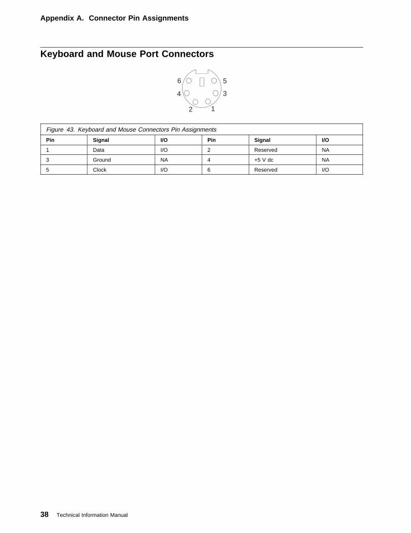
Keyboard and Mouse Port Connectors
6
4
2 1
3
5
Figure 43. Keyboard and Mouse Connectors Pin Assignments
Pin Signal I/O Pin Signal I/O
1 Data I/O 2 Reserved NA
3 Ground NA 4 +5 V dc NA
5 Clock I/O 6 Reserved I/O
38 Technical Information Manual

Appendix A. Connector Pin Assignments
ISA Connectors
A1
B1
A31
B31
C1
D1
C18
D18
Note: The ISA connectors are part of the riser card.
Figure 44 (Page 1 of 2). ISA Connector Pin Assignments
Pin Signal I/O Pin Signal I/O
B1 GROUND NA A1 IOCHCK# I
B2 RESET DRV O A2 SD7 I/O
B3 +5 V dc NA A3 SD6 I/O
B4 IRQ2 I A4 SD5 I/O
B5 -5 V dc NA A5 SD4 I/O
B6 DRQ2 I A6 SD3 I/O
B7 -12 V dc NA A7 SD2 I/O
B8 OWS# I A8 SD1 I/O
B9 +12 V dc NA A9 SD0 I/O
B10 GROUND NA A10 IOCHRDY I
B11 SMEMW# O A11 AEN O
B12 SMEMR# O A12 SA19 I/O
B13 IOW# I/O A13 SA18 I/O
B14 IOR# I/O A14 SA17 I/O
B15 DACK3# O A15 SA16 I/O
B16 DRQ3 I A16 SA15 I/O
B17 DACK1# O A17 SA14 I/O
B18 DRQ1 I A18 SA13 I/O
B19 REFRESH# I/O A19 SA12 I/O
B20 CLK O A20 SA11 I/O
B21 IRQ7 I A21 SA10 I/O
B22 IRQ6 I A22 SA9 I/O
B23 IRQ5 I A23 SA8 I/O
B24 IRQ4 I A24 SA7 I/O
B25 IRQ3 I A25 SA6 I/O
B26 DACK2# O A26 SA5 I/O
B27 TC O A27 SA4 I/O
B28 BALE O A28 SA3 I/O
B29 +5 V dc NA A29 SA2 I/O
B30 OSC O A30 SA1 I/O
B31 GROUND NA A31 SA0 I/O
D1 MEMCS16# I C1 SBHE# I/O
D2 IOCS16# I C2 LA23 I/O
D3 IRQ10 I C3 LA22 I/O
Appendix A. Connector Pin Assignments 39

Appendix A. Connector Pin Assignments
Figure 44 (Page 2 of 2). ISA Connector Pin Assignments
Pin Signal I/O Pin Signal I/O
D4 IRQ11 I C4 LA21 I/O
D5 IRQ12 I C5 LA20 I/O
D6 IRQ15 I C6 LA19 I/O
D7 IRQ14 I C7 LA18 I/O
D8 DACK0# O C8 LA17 I/O
D9 DRQ0 I C9 MEMR# I/O
D10 DACK5# O C10 MEMW# I/O
D11 DRQ5 I C11 SD8 I/O
D12 DACK6# O C12 SD9 I/O
D13 DRQ6 I C13 SD10 I/O
D14 DACK7# O C14 SD11 I/O
D15 DRQ7 I C15 SD12 I/O
D16 +5 V dc NA C16 SD13 I/O
D17 MASTER# I C17 SD14 I/O
D18 GROUND NA C18 SD15 I/O
40 Technical Information Manual

Appendix A. Connector Pin Assignments
PCI Connector
Note: The PCI connectors are part of the riser card.
Figure 45 (Page 1 of 2). PCI Connector Pin Assignments
Pin Signal I/O Pin Signal I/O
A1 TRST# O B1 −12 V dc NA
A2 +12 V dc NA B2 TCK O
A3 TMS O B3 Ground NA
A4 TDI O B4 TDO I
A5 +5 V dc NA B5 +5 V dc NA
A6 INTA# I B6 +5 V dc NA
A7 INTC# I B7 INTB# I
A8 +5 V dc NA B8 INTD# I
A9 Reserved NA B9 PRSNT1# I
A10 +5 V dc (I/O) NA B10 Reserved NA
A11 Reserved NA B11 PRSNT2 I
A12 Ground NA B12 Ground NA
A13 Ground NA B13 Ground NA
A14 Reserved NA B14 Reserved NA
A15 RST# O B15 Ground NA
A16 +5 V dc (I/O) NA B16 CLK O
A17 GNT# O B17 Ground NA
A18 Ground NA B18 REQ# I
A19 Reserved NA B19 +5 V dc (I/O) NA
A20 Address/Data 30 I/O B20 Address/Data 31 I/O
A21 +3.3 V dc NA B21 Address/Data 29 I/O
A22 Address/Data 28 I/O B22 Ground NA
A23 Address/Data 26 I/O B23 Address/Data 27 I/O
A24 Ground I/O B24 Address/Data 25 NA
A25 Address/Data 24 I/O B25 +3.3 V dc NA
A26 IDSEL O B26 C/BE 3# I/O
A27 +3.3 V dc NA B27 Address/Data 23 I/O
A28 Address/Data 22 I/O B28 Ground NA
A29 Address/Data 20 I/O B29 Address/Data 21 I/O
A30 Ground I/O B30 Address/Data 19 NA
A31 Address/Data 18 I/O B31 +3.3 V dc NA
A32 Address/Data 16 I/O B32 Address/Data 17 I/O
A33 +3.3 V dc NA B33 C/BE 2# I/O
A34 FRAME# I/O B34 Ground NA
A35 Ground NA B35 IRDY# I/O
A36 TRDY# I/O B36 +3.3 V dc NA
A37 Ground NA B37 DEVSEL# I/O
A38 STOP# I/O B38 Ground NA
A39 +3.3 V dc NA B39 LOCK# I/O
Appendix A. Connector Pin Assignments 41

Appendix A. Connector Pin Assignments
Figure 45 (Page 2 of 2). PCI Connector Pin Assignments
Pin Signal I/O Pin Signal I/O
A40 SDONE I/O B40 PERR# I/O
A41 SBO# I/O B41 +3.3 V dc NA
A42 Ground NA B42 SERR# I/O
A43 +3.3 V dc NA B43 +3.3 V dc NA
A44 C/BE(1)# I/O B44 C/BE 1# I/O
A45 Address/Data 14 I/O B45 Address/Data 14 I/O
A46 Ground NA B46 Ground NA
A47 Address/Data 12 I/O B47 Address/Data 12 I/O
A48 Address/Data 10 I/O B48 Address/Data 10 I/O
A49 Ground NA B49 Ground NA
A50 Key NA B50 Key NA
A51 Key NA B51 Key NA
A52 Address/Data 8 I/O B52 Address/Data 8 I/O
A53 Address/Data 7 I/O B53 Address/Data 7 I/O
A54 +3.3 V dc NA B54 +3.3 V dc NA
A55 Address/Data 5 I/O B55 Address/Data 5 I/O
A56 Address/Data 3 I/O B56 Address/Data 3 I/O
A57 Ground NA B57 Ground NA
A58 Address/Data 1 I/O B58 Address/Data 1 I/O
A59 +5 V dc (I/O) NA B59 +5 V dc (I/O) NA
A60 ACK64# I/O B60 ACK64# I/O
A61 +5 V dc NA B61 +5 V dc NA
A62 +5 V dc NA B62 +5 V dc NA
42 Technical Information Manual

Appendix A. Connector Pin Assignments
Wake on LAN and Modem/Ring Wakeup Connectors
Power Supply Connectors
Figure 46. J27 Modem Ring
Pin Description
1 Ground
2 External Wake Up on Ring
Figure 47. J28 Wake on LAN
Pin Description
1 Ground
2 External Wake on LAN
Figure 48. Pin Assignments for Power Supply Connectors
Connector Location Pin 1 Pin 2 Pin 3 Pin 4 Pin 5 Pin 6
P1 System Board PWRGOOD +5 V +12 V -12 V GND GND
P2 System Board GND GND -5 V +5 V +5 V +5 V
P3 3.5" Diskette Drive +5 V GND GND +12 V – –
P4 DASD +12 V GND GND +5 V – –
P5 1 DASD +12 V GND GND +5 V – –
P9 2 System Board +5 V CONTROL GND – – –
P10 Riser 3 V +3.3 V +3.3 V +3.3 V GND GND GND
P11 System Board 3 V +3.3 V +3.3 V +3.3 V GND GND GND
P12 LAN +5 V CONTROL GND – – –
1 Connectors provided only with the 145W power supply.
2 AUX 5
Appendix A. Connector Pin Assignments 43
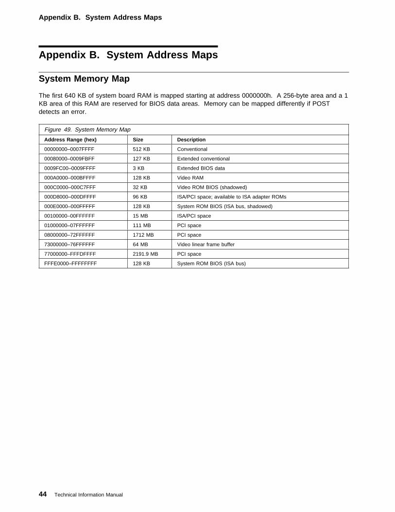
Appendix B. System Address Maps
Appendix B. System Address Maps
System Memory Map
The first 640 KB of system board RAM is mapped starting at address 0000000h. A 256-byte area and a 1KB area of this RAM are reserved for BIOS data areas. Memory can be mapped differently if POSTdetects an error.
Figure 49. System Memory Map
Address Range (hex) Size Description
00000000–0007FFFF 512 KB Conventional
00080000–0009FBFF 127 KB Extended conventional
0009FC00–0009FFFF 3 KB Extended BIOS data
000A0000–000BFFFF 128 KB Video RAM
000C0000–000C7FFF 32 KB Video ROM BIOS (shadowed)
000D8000–000DFFFF 96 KB ISA/PCI space; available to ISA adapter ROMs
000E0000–000FFFFF 128 KB System ROM BIOS (ISA bus, shadowed)
00100000–00FFFFFF 15 MB ISA/PCI space
01000000–07FFFFFF 111 MB PCI space
08000000–72FFFFFF 1712 MB PCI space
73000000–76FFFFFF 64 MB Video linear frame buffer
77000000–FFFDFFFF 2191.9 MB PCI space
FFFE0000–FFFFFFFF 128 KB System ROM BIOS (ISA bus)
44 Technical Information Manual
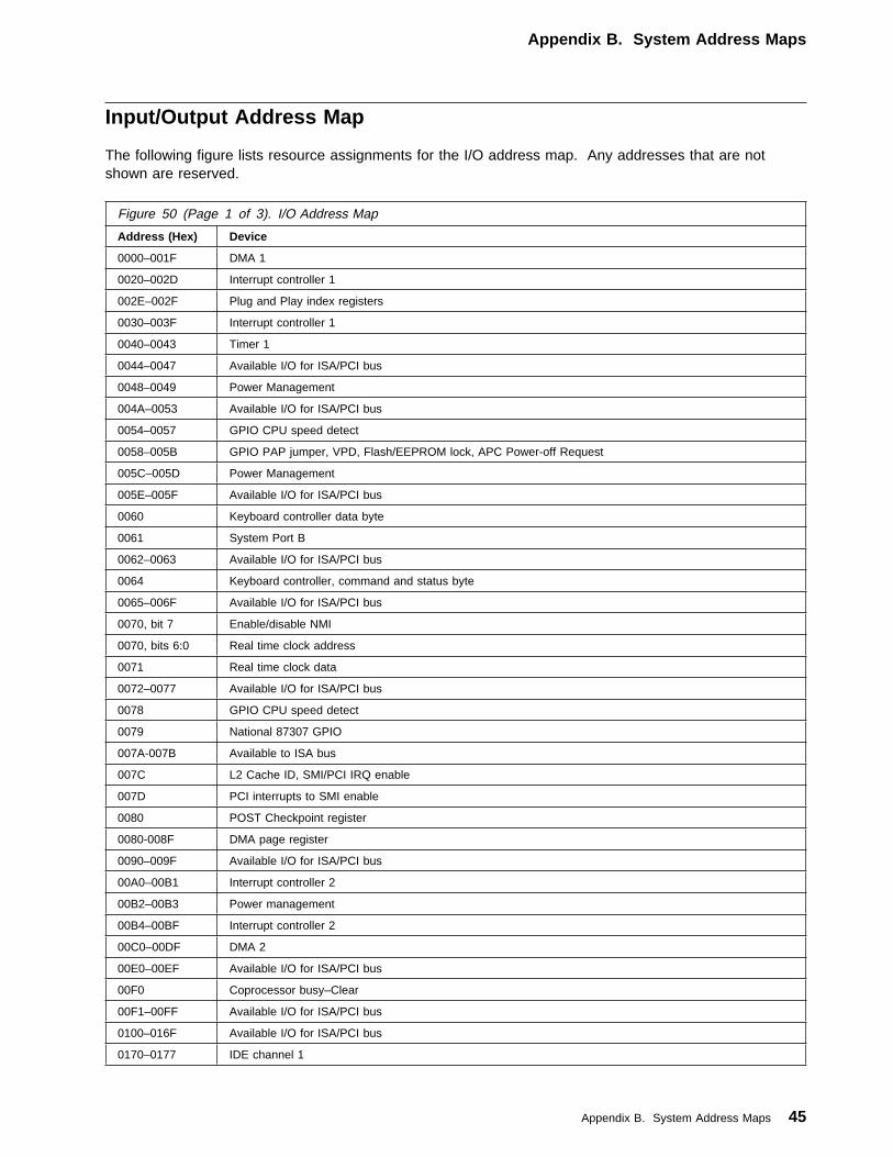
Appendix B. System Address Maps
Input/Output Address Map
The following figure lists resource assignments for the I/O address map. Any addresses that are notshown are reserved.
Figure 50 (Page 1 of 3). I/O Address Map
Address (Hex) Device
0000–001F DMA 1
0020–002D Interrupt controller 1
002E–002F Plug and Play index registers
0030–003F Interrupt controller 1
0040–0043 Timer 1
0044–0047 Available I/O for ISA/PCI bus
0048–0049 Power Management
004A–0053 Available I/O for ISA/PCI bus
0054–0057 GPIO CPU speed detect
0058–005B GPIO PAP jumper, VPD, Flash/EEPROM lock, APC Power-off Request
005C–005D Power Management
005E–005F Available I/O for ISA/PCI bus
0060 Keyboard controller data byte
0061 System Port B
0062–0063 Available I/O for ISA/PCI bus
0064 Keyboard controller, command and status byte
0065–006F Available I/O for ISA/PCI bus
0070, bit 7 Enable/disable NMI
0070, bits 6:0 Real time clock address
0071 Real time clock data
0072–0077 Available I/O for ISA/PCI bus
0078 GPIO CPU speed detect
0079 National 87307 GPIO
007A-007B Available to ISA bus
007C L2 Cache ID, SMI/PCI IRQ enable
007D PCI interrupts to SMI enable
0080 POST Checkpoint register
0080-008F DMA page register
0090–009F Available I/O for ISA/PCI bus
00A0–00B1 Interrupt controller 2
00B2–00B3 Power management
00B4–00BF Interrupt controller 2
00C0–00DF DMA 2
00E0–00EF Available I/O for ISA/PCI bus
00F0 Coprocessor busy–Clear
00F1–00FF Available I/O for ISA/PCI bus
0100–016F Available I/O for ISA/PCI bus
0170–0177 IDE channel 1
Appendix B. System Address Maps 45

Appendix B. System Address Maps
Figure 50 (Page 2 of 3). I/O Address Map
Address (Hex) Device
01F0–01F7 IDE channel 0
0220–0227 National 87307, serial port 3 or 4
0278–027F National 87307, parallel port 3
02E8–02EF National 87307, serial port 3 or 4
02F8–02FF National 87307, serial port 2
0338–033F National 87307, serial port 3 or 4
0340–0373 Available I/O for ISA/PCI bus
0374–0377 IDE channel 1
0377, bit 7 IDE, diskette change
0378–037F National 87307, parallel port 2
03B4–03BB CL-GD5446 Video chip
03BC–03BE National 87307, parallel port 1 (system board)
03BF–03DF CL-GD5446 Video chip
03E8–03EF National 87307, serial port 3 or 4
03F0–03F5 National 87307, diskette channel 0
03F6 IDE channel 0
03F7, bit 7 IDE, diskette change
03F7, bits 6:0 IDE channel 0
03F8–03FF National 87307, serial port 1 (system board)
04D0–04D1 Interrupt Edge/level control 1 and 2
0CF8–0CFB PCI configuration address register
0CF9 Reset control register
0CFC–0CFF PCI configuration data registers
42E8–42E9 CL-GD5446 Video
4AE8–4AE9 CL-GD5446 Video
8180–8187 CL-GD5446 Video
8190–819B CL-GD5446 Video
81A0 CL-GD5446 Video
81C0–81FF CL-GD5446 Video
82E8 CL-GD5446 Video
86E8 CL-GD5446 Video
8AE8 CL-GD5446 Video
8EE8 CL-GD5446 Video
92E8 CL-GD5446 Video
96E8 CL-GD5446 Video
9AE8 CL-GD5446 Video
9EE8 CL-GD5446 Video
A2E8 CL-GD5446 Video
A6E8 CL-GD5446 Video
AAE8 CL-GD5446 Video
AEE8 CL-GD5446 Video
B2E8 CL-GD5446 Video
B6E8 CL-GD5446 Video
46 Technical Information Manual

Appendix B. System Address Maps
Figure 50 (Page 3 of 3). I/O Address Map
Address (Hex) Device
BAE8 CL-GD5446 Video
BEE8 CL-GD5446 Video
E2E8 CL-GD5446 Video
E2EA CL-GD5446 Video
Appendix B. System Address Maps 47

Appendix B. System Address Maps
DMA I/O Address Map
The following figure lists resource assignments for the DMA address map. Any addresses that are notshown are reserved.
Figure 51 (Page 1 of 2). DMA I/O Addresses
Address (Hex) Description Bits Byte Pointer
0000 Channel 0, Memory Address register 00–15 Yes
0001 Channel 0, Transfer Count register 00–15 Yes
0002 Channel 1, Memory Address register 00–15 Yes
0003 Channel 1, Transfer Count register 00–15 Yes
0004 Channel 2, Memory Address register 00–15 Yes
0005 Channel 2, Transfer Count register 00–15 Yes
0006 Channel 3, Memory Address register 00–15 Yes
0007 Channel 3, Transfer Count register 00–15 Yes
0008 Channels 0–3, Read Status/Write Command register 00–07
0009 Channels 0–3, Write Request register 00–02
000A Channels 0–3, Write Single Mask register bits 00–02
000B Channels 0–3, Mode register (write) 00–07
000C Channels 0–3, Clear byte pointer (write) N/A
000D Channels 0–3, Master clear (write)/temp (read) 00–07
000E Channels 0–3, Clear Mask register (write) 00–03
000F Channels 0–3, Write All Mask register bits 00–03
0081 Channel 2, Page Table Address register 3 00–07
0082 Channel 3, Page Table Address register 3 00–07
0083 Channel 1, Page Table Address register 3 00–07
0087 Channel 0, Page Table Address register 3 00–07
0089 Channel 6, Page Table Address register 3 00–07
008A Channel 7, Page Table Address register 3 00–07
008B Channel 5, Page Table Address register 3 00–07
008F Channel 4, Page Table Address/Refresh register 00–07
00C0 Channel 4, Memory Address register 00–15 Yes
00C2 Channel 4, Transfer Count register 00–15 Yes
00C4 Channel 5, Memory Address register 00–15 Yes
00C6 Channel 5, Transfer Count register 00–15 Yes
00C8 Channel 6, Memory Address register 00–15 Yes
00CA Channel 6, Transfer Count register 00–15 Yes
00CC Channel 7, Memory Address register 00–15 Yes
00CE Channel 7, Transfer Count register 00–15 Yes
00D0 Channels 4–7, Read Status/Write Command register 00–07
00D2 Channels 4–7, Write Request register 00–02
00D4 Channels 4–7, Write Single Mask register bit 00–02
00D6 Channels 4–7, Mode register (write) 00–07
00D8 Channels 4–7, Clear byte pointer (write) N/A
00DA Channels 4–7, Master clear (write)/temp (read) 00–07
48 Technical Information Manual

Appendix B. System Address Maps
Figure 51 (Page 2 of 2). DMA I/O Addresses
Address (Hex) Description Bits Byte Pointer
00DC Channels 4–7, Clear Mask register (write) 00–03
00DE Channels 4–7, Write All Mask register bits 00–03
00DF Channels 5–7, 8- or 16-bit mode select 00–07
3 Upper byte of memory address register.
Appendix B. System Address Maps 49

Appendix C. IRQ and DMA Channel Assignments
Appendix C. IRQ and DMA Channel Assignments
The following figures list the interrupt request (IRQ) and direct memory access (DMA) channelassignments.
Figure 52. IRQ Channel Assignments
IRQ System Resource
NMI Critical system error
SMI System/power management interrupt
0 Reserved (internal timer)
1 Reserved (keyboard)
2 Reserved (cascade interrupt from slave)
3 Serial port 2 4
4 Serial port 1 4
5 Parallel port 2 4
6 Diskette controller 4
7 Parallel port 1 4
8 Reserved (real-time clock)
9 Video adapter 4
10 ISA/PCI bus
11 ISA/PCI bus
12 Mouse port 4
13 Reserved (math coprocessor)
14 IDE Channel 1 4
15 IDE Channel 2 4
4 If not assigned, this resource is available for the ISA/PCI bus.
50 Copyright IBM Corp. October 1997

Appendix C. IRQ and DMA Channel Assignments
Figure 53. DMA Channel Assignments
DMA Channel Data Width SystemResource
0 ISA bus 8 bits
1 ISA bus 8 bits
2 Reserved (diskette drive) 8 bits
3 ECP parallel port 5 8 bits
4 Reserved (cascade channel) –
5 ISA bus 16 bits
6 ISA bus 16 bits
7 ISA bus 16 bits
5 If not assigned, this resource is available for the ISA bus.
Appendix C. IRQ and DMA Channel Assignments 51

Appendix D. Error Codes
Appendix D. Error Codes
The following figures list the POST error codes and beep error codes for the computer.
POST Error Codes
POST error messages appear when POST finds problems with the hardware during power-on or when achange in the hardware configuration is found. POST error messages are 3-, 4-, 5-, 8-, or 12-characteralphanumeric messages. An x in an error message can represent any number.
Figure 54 (Page 1 of 2). POST Error Codes
Code Description
101 Interrupt failure
102 Timer failure
103 Timer-interrupt failure
104 protected mode failure
105 last 8042 command not accepted –keyboard failure
106 System board failure
108 Timer bus failure
109 low MB chip select test
110 System board parity error 1 (system board parity latch set)
111 I/O parity error 2 (I/O channel check latch set)
112 I/O channel check error
113 I/O channel check error
114 external ROM checksum error
115 DMA error
116 System board port read/write error
120 Microprocessor test error
121 Hardware error
151 Real time clock failure
161 Bad CMOS Battery
162 CMOS RAM checksum/configuration error
163 Clock not updating
164 CMOS RAM memory size does not match
167 Clock not updating
175 Riser card or system board error
176 System cover has been removed
177 Corrupted administrator password
178 Riser card or system board error
183 Administrator password has been set and must be entered
184 Password removed due to checksum error
185 Corrupted boot sequence
186 System board or hardware security error
189 More than three password attempts were made to access system
201 Memory date error
52 Copyright IBM Corp. October 1997

Appendix D. Error Codes
Figure 54 (Page 2 of 2). POST Error Codes
Code Description
202 Memory address line error 00-15
203 Memory address line error 16-23
221 ROM to RAM remapping error
225 Unsupported memory type installed or memory pair mismatch
301 Keyboard error
302 Keyboard error
303 Keyboard to system board interface error
304 Keyboard clock high
305 No keyboard +5 V
601 Diskette drive or controller error
602 Diskette IPL boot record not valid
604 Unsupported diskette drive installed
605 POST cannot unlock diskette drive
662 Diskette drive configuration error
762 Math coprocessor configuration error
11xx Serial port error (xx = serial port number)
1762 Hard disk configuration error
1780 Hard disk 0 failed
1781 Hard disk 1 failed
1782 Hard disk 2 failed
1783 Hard disk 3 failed
1800 PCI adapter has requested an unavailable hardware interrupt
1801 PCI adapter has requested an unavailable memory resource
1802 PCI adapter has requested an unavailable I/O address space, or a defective adapter
1803 PCI adapter has requested an unavailable memory address space, or a defective adapter
1804 PCI adapter has requested unavailable memory addresses
1805 PCI adapter ROM error
1962 Boot sequence error
2401 System board video error
8601 System board - keyboard/pointing device error
8602 Pointing device error
8603 Pointing device or system board error
12092 Level 1 cache error (Processor chip)
12094 Level 2 cache error
16101 Riser card battery is dead
I9990301 Hard disk failure
I9990305 No operating system found
Appendix D. Error Codes 53

Appendix D. Error Codes
Beep Codes
For the following beep codes, the numbers indicate the sequence and number of beeps. For example, a“2-3-2” error symptom (a burst of two beeps, three beeps, then a burst of two beeps) indicates a memorymodule problem.
Figure 55. Beep Codes
Beep Code Probable Cause
1-1-3 CMOS write/read failure
1-1-4 BIOS ROM checksum failure
1-2-1 Programmable interval timer test failure
1-2-2 DMA initialization failure
1-2-3 DAM page register write/read test failure
1-2-4 RAM refresh verification failure
1-3-1 1st 64 K RAM test failure
1-3-2 1st 64 K RAM parity test failure
2-1-1 Slave DMA register test in progress or failure
2-1-2 Master DMA register test in progress or failure
2-1-3 Master interrupt mask register test failure
2-1-4 Slave interrupt mask register test failure
2-2-2 Keyboard controller test failure
2-3-2 Screen memory test in progress or failure
2-3-3 Screen retrace tests in progress or failure
3-1-1 Timer tick interrupt test failure
3-1-2 Interval timer channel 2 test failure
3-1-4 Time-of-Day clock test failure
3-2-4 Comparing CMOS memory size against actual
3-3-1 Memory size mismatch occurred
54 Technical Information Manual

Appendix E. Notices and Trademarks
Appendix E. Notices and Trademarks
References in this publication to IBM products, programs, or services do not imply that IBM intends tomake these available in all countries in which IBM operates. Any reference to an IBM product, program,or service is not intended to state or imply that only that IBM product, program, or service may be used.Subject to IBM’s valid intellectual property or other legally protectable rights, any functionally equivalentproduct, program, or service may be used instead of the IBM product, program, or service. The evaluationand verification of operation in conjunction with other products, except those expressly designated by IBM,are the responsibility of the user.
IBM may have patents or pending patent applications covering subject matter in this document. Thefurnishing of this document does not give you any license to these patents. You can send licenseinquiries, in writing, to:
IBM Director of Licensing IBM Corporation
500 Columbus Avenue Thornwood, NY 10594 U.S.A.
The following terms are trademarks of the IBM Corporation in the United States or other countries or both:
Microsoft and Windows are trademarks or registered trademarks of Microsoft Corporation.
Other company, product, and service names may be trademarks or service marks of others.
AT Personal Computer ATIBM SurePathPC 300 Wake on LAN
Copyright IBM Corp. October 1997 55

References
� 82439HX PCISet System Controller (TXC)Source: Intel Corporation; available athttp://www.intel.com/design/pcisets/datashts
� 82371SB PCI ISA IDE Xcelerator (PIIX3)Source: Intel Corporation; available athttp://www.intel.com/design/pcisets/datashts
� Advanced Power Management (APM) BIOSInterface Specification 1.2/Source: Intel Corporation
� AT Attachment Interface with ExtensionsSource: American National Standard of AccreditedStandards Committee
� Extended Capabilities Port: Specification KitSource: Microsoft Corporation
� Intel Microprocessor and Peripheral ComponentLiteratureSource: Intel Corporation
� PCI BIOS Specification 2.0Source: PCI Special Interest Group
� PCI Local Bus Specification 2.1Source: PCI Special Interest Group
� Plug and Play BIOS Specification 1.1Source: Microsoft Corporation; available athttp://www.microsoft.com/hwdev
� Plug and Play BIOS Specification, Errata andClarifications 1.0Source: Microsoft Corporation
� Universal Serial Bus SpecificationsSource: http://www.teleport.com/˜usb
� Video Electronics Standards Association 1.2Source: http://www.vesa.org
56 Copyright IBM Corp. October 1997

Index
Index
Aaddress map
DMA 48I/O 45system memory 44
advanced power management 26altitude 17APM 26
Bbeep codes 54BIOS 25BIOS data areas 44bus
IDE 6ISA 6, 12PCI 6, 12universal serial bus 7
bypassing BIOS 29
Ccables 17, 19chipset 4, 9clock, real-time 11CMOS RAM 11compatibility
hardware 27software 30
component maximum current 23configuration/setup utility 25connector
DIMM 32diskette drive 35IDE 34ISA bus 39keyboard/mouse ports 38modem/ring wakeup 43monitor 35parallel port 37PCI 41power supply 43serial ports 37USB 35Wake on LAN 43
controllerdiskette drive 9, 29I/O 9keyboard/mouse 10parallel 10serial 9
copy protection 29current, electrical 18, 20
Ddepth, system unit 17, 19diagnostic programs 26DIMM connectors 5diskette drive
change signal 29compatibility 29controller 9write current 29
diskette drives 29DMA (direct memory access) channel assignments 51
Eelectromagnetic compatibility 17environment, operating 16, 19error codes, POST 52ethernet port 11external cache (L2) 4
Ffault, overvoltage 24flash EEPROM 12flash update 26frequency 18, 20frequency, input power 21
GGPIO ports 11
Hhard disk drive
compatibility 29controller 29
hardware compatibility 27hardware interrupts 28heat output 18, 20height, system unit 17, 19humidity 18, 20
II/O
controller 9features 15
Copyright IBM Corp. October 1997 57

Index
I/O address map 45IDE interface 6information, related viiiinput power
frequency 21requirements 21voltage 21
interrupt request assignments 50ISA
bus 6connectors 12
Jjumper
configuration 14locations (system board) 13
Kkeyboard cable 17, 19
LL2 cache (external) 4level-sensitive interrupts 28load currents 23
Mmachine-sensitive programs 30measurements, system unit 17, 19memory
error in 44map, system 44RAM 44system memory map 44
messages, POST error 52microprocessor
features 3upgrade socket 3
modes, power management 26
Nnetwork enablement 2
Oordering publications viiioutputs, power supply 23overvoltage fault 24
Pparallel port 10
PCIbus 6connectors 12
Pentium microprocessor 3Plug and Play 25polling mechanism 30port
ethernet 11GPIO 11keyboard/mouse 10parallel 10serial 9
POST 25, 44POST error codes 52power
cable 17, 19consumption 26description 21for components 23load currents 23management modes 26output protection 24outputs 23specifications 18, 20
protection, power supply 24publications, related viii
QQAPlus/PRO 26QAPlus/WIN-WIN 26
RRAM (random access memory) 44random access memory (RAM) 44references 56related information viiireserved
areas ixriser card 12
SSDRAM (synchronous dynamic random access
memory) 5serial port 9short circuit 24size, system unit 17, 19socket, microprocessor upgrade 3software
compatibility 30interrupts 30
specificationsmechanical 16physical 19
58 Technical Information Manual
Index
switches, configuration 14system
memory maps 44specifications 16, 19
system board
Ttemperature 17, 20token ring port 11
Uuniversal serial bus
connectors 35port 7technology 7
Vvideo
subsystem 8voltage, input power 21voltage, output power 22
WWake on LAN 2Wake Up On Ring 2warning, reserved areas ixweight, system unit 17, 19width, system unit 17, 19write current, diskette 29
Index 59

IBM
Part Number:
Printed in U.S.A.