Embed Size (px)
Citation preview

TECHNICAL MANUAL
TM 11-6625-3135-12
OPERATOR’S AND ORGANIZATIONALMAINTENANCE MANUAL
OSCILLOSCOPEAN/USM-488
(NSN 6625 -01-1 87-7847)4
This copy is a reprint which includes current
pages from Change 1.
HEADQUARTERS, DEPARTMENT OF THE ARMY
1 OCTOBER 1986
TM 11-6625-3135-12
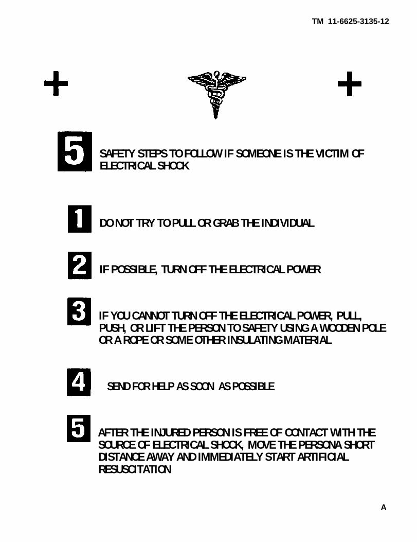
SAFETY STEPS TO FOLLOW IF SOMEONE IS THE VICTIM OFELECTRICAL SHOCK
DO NOT TRY TO PULL OR GRAB THE INDIVIDUAL
IF POSSIBLE, TURN OFF THE ELECTRICAL POWER
IF YOU CANNOT TURN OFF THE ELECTRICAL POWER, PULL,PUSH, OR LIFT THE PERSON TO SAFETY USING A WOODEN POLEOR A ROPE OR SOME OTHER INSULATING MATERIAL
SEND FOR HELP AS SOON AS POSSIBLE
AFTER THE INJURED PERSON IS FREE OF CONTACT WITH THESOURCE OF ELECTRICAL SHOCK, MOVE THE PERSONA SHORTDISTANCE AWAY AND IMMEDIATELY START ARTIFICIALRESUSCITATION
A

TM 11-6625-3135-12
WARNING
HIGH VOLTAGE
is used in the operation of this equipment
DEATH ON CONTACT
may result if personnel fail to observe safety precautions
Never work on electronic equipment unless there is another person nearby who is familiar with theopera! ion and hazards of the equipment and who is competent in administering first aid. When thetechnician is aided by operators, they must be warned about dangerous areas.
A periodic review of safety precautions in TB 385-4, Safety Precautions for Maintenance ofElectrical/Electronic Equipment, is recommended. When the equipment is operated with coversremoved, DO NOT TOUCH exposed connections or components. MAKE CERTAIN you are notgrounded when making connections or adjusting components inside the test instrument.
Be careful not to contact high-voltage connections or 115 volt ac input connections wheninstalling or operating this equipment.
Whenever the nature of the operation permits, keep one hand away from the equipment to reducethe hazard of current flowing through the body.
WARNING Do not be misled by the term “low voltage”. Potentials as low as50 volts may cause death under adverse conditions.
For Artficial Respiration. refer to FM 21-11.
B

INTRODUCTION
OPERATING INSTRUCTIONS
ORGANIZATIONAL MAINTENANCE INSTRUCTIONS
SUBJECT INDEX
TM 11-6625-3135-12
Technical Manual HEADQUARTERSDEPARTMENT OF THE ARMY
No. 11-6625-3135-12 Washington, DC, 1 October 1986
OPERATOR’S AND ORGANIZATIONAL MAINTENANCE MANUALFOR
OSCILLOSCOPE AN/USM-488(NSN 6625-01-187-7847)
REPORTING ERRORS AND RECOMMENDING IMPROVEMENTS
You can help improve this manual. If you find any mistakes or if you know of a way to improve theprocedures, please let us know. Mail your letter, DA Form 2028 (Recommended Changes toPublications and Blank Forms), or DA Form 2028-2 located in the back of this manual direct to:Commander, US Army Communications-Electronics Command and Fort Monmouth, ATTN:AMSEL-LC-LM-LT, Fort Monmouth, New Jersey 07703-5000. In either case, a reply will befurnished direct to you.
PageHOW TO USE THIS MANUAL . . . . . . . . . . . . . . . . . . . . .
. . . . . . . . . . . . . . . . . . . . . . . . . . .CHAPTER 1Section I General Information . . . . . . . . . . . . . . . . . . . . . . . . . . . . . . . . . . . . . . . . . . . . . . . . . .
II EQUIPPMENT DESCRIPTION . . . . . . . . . . . . . . . . . . . . . . . . . . . . . . . . . . . . . . . . . . . . . . .III Technical Principles of Operation . . . . . . . . . . . . . . . . . . . . . . . . . . . . . . . . . . . .
iii1-11-11-41-10
CHAPTER 2 . . . . . . . . . . . . . . . . .Section I Description and Use of Operator’s Controls and Indicators . . . . . . . . . .
II Operator Preventive Maintenance Checks and Services (PMCS) . . . . . .III Operation Under Usual Conditions . . . . . . . . . . . . . . . . . . . . . . . . . . . . . . . . . . . IV Operation Under Unusual Conditions . . . . . . . . . . . . . . . . . . . . . . . . . . . . . . . .
2-12-22-82-112-44
CHAPTER 3Section I
IIIIIIVV
APPENDIX ABCD
. . . .Repair Parts, Special Tools; (TMDE); and Support Equipment . . . . . .Service Upon Receipt . . . . . . . . . . . . . . . . . . . . . . . . . . . . . . . . . . . . . . . . . . . . . . . . .Troubleshooting . . . . . . . . . . . . . . . . . . . . . . . . . . . . . . . . . . . . . . . . . . . . . . . . . . . . . .Maintenance Procedures . . . . . . . . . . . . . . . . . . . . . . . . . . . . . . . . . . . . . . . . . . . . . .Preparation for Storage or Shipment . . . . . . . . . . . . . . . . . . . . . . . . . . . . . . .
3-13-13-23-33-53-12
A-1
B-1C-1
D-1I-1
Change 1 i/(ii blank)


TM 11-6625-3135-12
HOW TO USE THIS MANUAL
This manual tells you about your Oscilloscope AN/USM-488 andcontains instructions about how to use it while testing and maintainingother equipment.
The technical manual for the equipment you are maintaining will giveyou some guidance in the correct method to make certain connectionswhen testing and troubleshooting with the oscilloscope.
When you first receive your oscilloscope, start at the front of themanual and go all the way through to the back, and become familiarwith every part of the manual and the oscilloscope.
This manual has an edge index which will help you find specificinformation in a hurry. Simply spread the pages on the right edge of themanual until the printed blocks can be seen. Open the manual where theblock on the edge of the page lines up with your selected topic printed inthe front cover block.
iii

TM 11-6625-3135-12
Figure 1-1. Oscilloscope AN/USM-488
1-0

TM 11-6625-3135-12
CHAPTER 1INTRODUCTION
Para Page
Consolidated Index of Army Publications and Blank Forms. . . . . . . . . . . . . . . . . Destruction of Army Materiel to Prevent Enemy Use . . . . . . . . . . . . . . . . . . . . . . . . . . . .Euipment Characteristics, Capabilities, and Features. . . . . . . . . . . . . . . . . . . . . . . .Euipment Data . . . . . . . . . . . . . . . . . . . . . . . . . . . . . . . . . . Functional Description . . . . . . . . . . . . . . . . . . . . . . . . . . . . . . . . . . . . . . . . . . . . . . . . . . . . . . . .List of Abbreviations . . . . . . . . . . . . . . . . . . . . . . . . . . . . . . . . . . Location and Description of Major Components . . . . . . . . . . . . . . . . . . . . . . . . . . . .Maintenance Forms,Records,and Reports . . . . . . . . . . . . . . . . . . . . . . . . . . . . . . .Nomenclature Cross-Reference List . . . . . . . . . . . . . . . . . . . . . . . . . . . . . . . . . . . . .Preparation for Storage or Shipment . . . . . . . . . . . . . . . . . . . . . . . . . . . . .Reporting Equipment Improvement Recommendations (EIR) . . . . . . . . . . . . . .Safety, Care, and Handling . . . . . . . . . . . . . . . . . . . . . . . . . . . . . . . . . . . . . . . . . . .Scope . . . . . . . . . . . . . . . . . . . . . . . . . . . . . . . . . . . .Warranty Information . . . . . . . . . . . . . . . . . . . . . . . . . . . . . . . . . . . . . . . . . . . . . . . . . . . . . . . .
1-21-41-111-131-141-101-121-31-71-51-81-61-11-9
1-11-11-41-61-101-31-41-11-11-11-11-11-11-2
Section I. GENERAL INFORMATION1-1.SCOPEThis manual describes the Oscilloscope AN/USM-488 (oscilloscope) and provides instructions for operation, cleaning,inspection, and maintenance. Testing, troubleshooting, and repair procedures are provided for organizationalmaintenance personnel. The oscilloscope (fig. 1-1) is a portable, bench-type oscilloscope designed for general purposewaveform measurements using single-or dual-trace displays with normal or delayed sweep.1-2. CONSOLIDATED INDEX OF ARMY PUBLICATIONS AND BLANK FORMSRefer to the latest issue of DA Pam 25-30 to determine whether there are new editions, changes, or additional publicationspertaining to the equipment.1-3. MAINTENANCE FORMS, RECORDS, AND REPORTS
a. Reports of Maintenance and Unsatisfactory Equipment. Department of the Army forms andprocedures used for equipment maintenance will be those prescribed by DA Pam738-750, as contained in MaintenanceManagement Update.
b. Reporting of ltem and Packaging Discrepancies. Fill out and forward SF 364 (Report of Discrepancy(ROD)) as prescribed in AR 735-11-2/DLAR 4140.55/SECNAVINST 4355.18/AFR 400-54/MCO 4430.3J.
C. Transportation Discrepancy Report (TDR) (SF 361). Fill out and forward Transportation DiscrepancyReport (TDR) (SF 361) as prescribed in AR 55–38/NAVSUPINST 4610.33C/AFR 75-18/MCO P4610.19D/DLAR4500.15.1-4. DESTRUCTION OF ARMY ELECTRONICS MATERIEL TO PREVENT ENEMY USEDestruction of Army electronics materiel to prevent enemy use shall be in accordance with TM 750-244-2.1-5. PREPARATION FOR STORAGE OR SHIPMENTStorage and shipment procedures are in Chapter 3, Section V.1-6. SAFETY, CARE, AND HANDLINGObserve all WARNINGS, CAUTIONS, and NOTES in this manual. This equipment can be extremely dangerous ifthese instructions are not followed.1-7. NOMENCLATURE CROSS-REFERENCE LISTThis listing identifies approved nomenclature usage that is different from the official nomenclature:
Common Name Official NomenclatureOsccilloscope . . . . . . . . . . . . . . . . . . . . . . . . . .Oscilloscope AN/USM-488
Change 1 1-1

TM 11-6625-3135-12
1-8. REPORTING EQUIPMENT IMPROVEMENT RECOMMENDATIONS (EIR)If your oscillscope needs improvement, let us know. Send us an EIR. You, the user, are the only one who can tell us whatyou don’t like about your equipment. Let us know why you don’t like the design or performance. Put it on an SF 368(Product Quality Deficiency Report). Mail it to: Commander, US Army Communications-Electronics Command andFort Monmouth, ATTN: AMSEL-ED-PH, Fort Monmouth, New Jersey 07703-5000. We’ll send you a reply.
1-9. WARRANTY INFORMATION
Oscilloscope AN/USM488 is warranted by Tektronix Inc. for 1 year. The warranty starts on the date of purchase by theoriginal owner. Report all defects immaterial or workmanship to your supervisor who will take appropriate action throughyour organizational maintenance shop.
1-2
TM 11-6625-3135-12
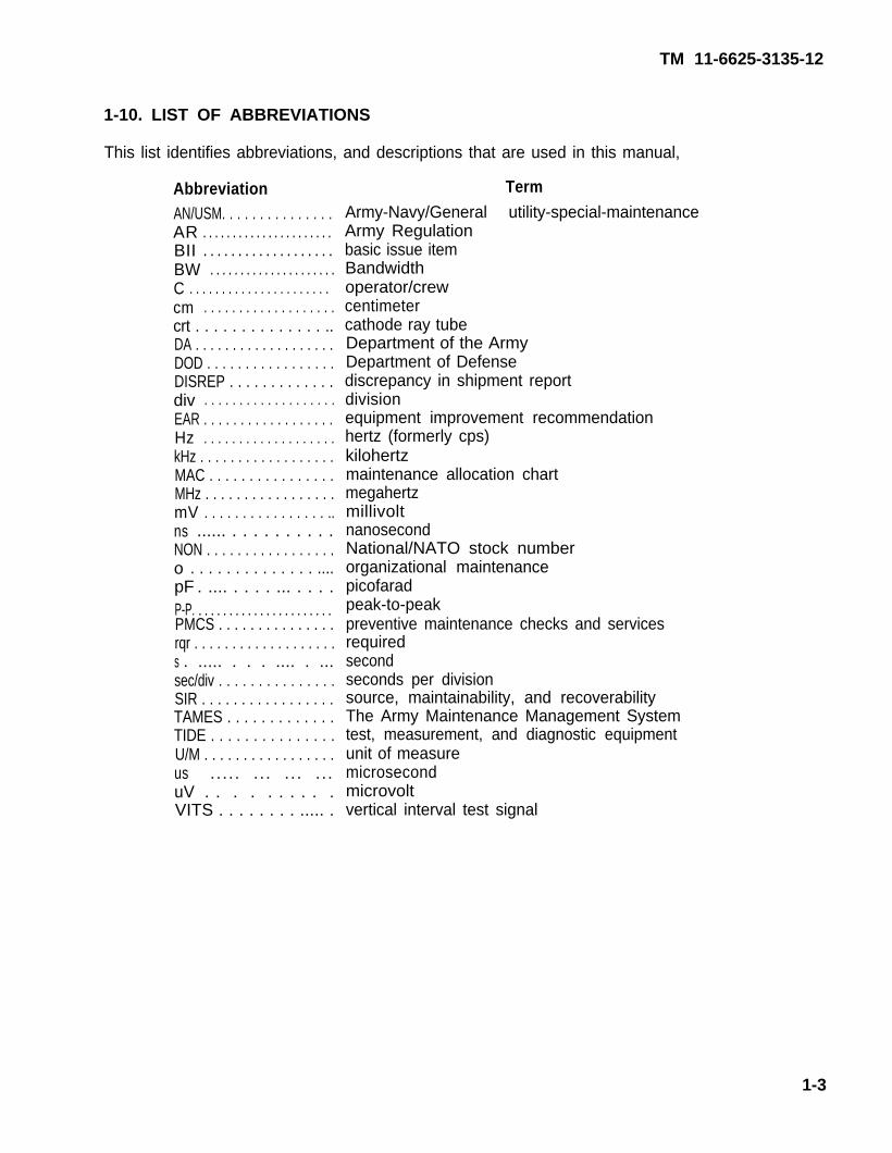
1-10. LIST OF ABBREVIATIONS
This list identifies abbreviations, and descriptions that are used in this manual,
AbbreviationAN/USM. . . . . . . . . . . . . . .AR . . . . . . . . . . . . . . . . . . . . . . BII . . . . . . . . . . . . . . . . . . .BW . . . . . . . . . . . . . . . . . . . . .C . . . . . . . . . . . . . . . . . . . . . . cm . . . . . . . . . . . . . . . . . . .crt . . . . . . . . . . . . . . ..DA . . . . . . . . . . . . . . . . . . .DOD . . . . . . . . . . . . . . . . .DISREP . . . . . . . . . . . . .div . . . . . . . . . . . . . . . . . . .EAR . . . . . . . . . . . . . . . . . .Hz . . . . . . . . . . . . . . . . . . .kHz . . . . . . . . . . . . . . . . . .MAC . . . . . . . . . . . . . . . .MHz . . . . . . . . . . . . . . . . .mV . . . . . . . . . . . . . . . . ..ns ...... . . . . . . . . . .NON . . . . . . . . . . . . . . . . .o . . . . . . . . . . . . . . ....pF . .... . . . . ... . . . .P-P. . . . . . . . . . . . . . . . . . . . . . . PMCS . . . . . . . . . . . . . . .rqr . . . . . . . . . . . . . . . . . . .s . ..... . . . .... . ...sec/div . . . . . . . . . . . . . . .SIR . . . . . . . . . . . . . . . . .TAMES . . . . . . . . . . . . .TIDE . . . . . . . . . . . . . . .U/M . . . . . . . . . . . . . . . . .us ..... . . . . . . . . .uV . . . . . . . . . .VITS . . . . . . . . ..... .
Term
Army-Navy/General utility-special-maintenanceArmy Regulationbasic issue itemBandwidthoperator/crewcentimetercathode ray tubeDepartment of the ArmyDepartment of Defensediscrepancy in shipment reportdivisionequipment improvement recommendationhertz (formerly cps)kilohertzmaintenance allocation chartmegahertzmillivoltnanosecondNational/NATO stock numberorganizational maintenancepicofaradpeak-to-peakpreventive maintenance checks and servicesrequiredsecondseconds per divisionsource, maintainability, and recoverabilityThe Army Maintenance Management Systemtest, measurement, and diagnostic equipmentunit of measuremicrosecondmicrovoltvertical interval test signal
1-3
TM 11-6625-3135-12
Section Il. EQUIPMENT DESCRIPTION
1-11. EQUIPMENT CHARACTERISTICS, CAPABILITIES, AND FEATURES
The oscilloscope is a rugged, lightweight, dual-channel instrument allowing visual evaluation ofelectrical circuits.
a. Characteristics.
Measures ac voltage and dc voltage
Measures frequency
Measures nondelayed time
Measures rise and fall times
Algebraically adds signals applied to channels 1 and 2
b. Capabilities and Features.
Vertical system provides calibrated deflection factors from 2 inV per division to 5 V per division
Trigger circuits enable stable triggering over full bandwidth of vertical system
Horizontal system provides calibrated sweep speeds from 0.5s per division to 50 ns per division
Horizontal system provides delayed sweep feature
. Magnifier circuit extends maximum sweep speed to 5 ns per division
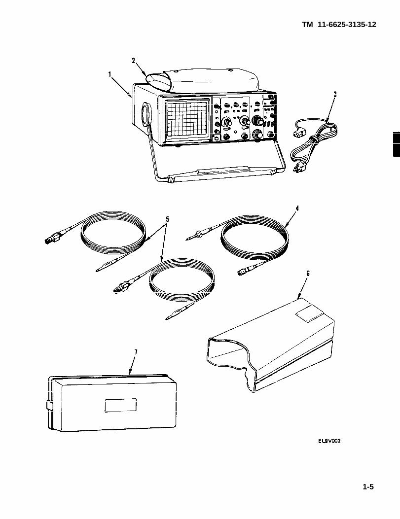
1-12. LOCATION AND DESCRIPTION OF MAJOR COMPONENTS
OSCILLOSCOPE (1) — A self-contained, multi-range measuring instrument that allows visualevaluation of electrical circuits. It measures and indicates various electrical characteristics needed totest and troubleshoot electrical equipment. The handle can be adjusted as a stand.
POUCH (2) — Provides storage for probes and small components.
AC POWER CORD (3) — Provides for operation from the ac power line.
1X PROBE PACKAGE (4) — Provides nonattenuated input to oscilloscope.
10X PROBE PACKAGE (5) – Attenuates input signal by factor of 10.
VIEWING HOOD (6) — Allows operator to view crt display in bright light.
COVER (7) — Protects crt screen and front panel controls.
1-4
TM 11-6625-3135-12
1-5

TM 11-6625-3135-12
1-13. EQUIPMENT DATA
VERTICAL DEFLECTION SYSTEM:Deflection Factor
Range . . . . . . . . . . . . . . . . . 2 m V to 5 V per divisionAccuracy at 52-95°F(15-350C) ±2%Accuracy at 32-122°F(0-500C). . . . . . . .. ±3%Range of VOLTS/DIV Control . . . . . . . . . . . . Continuously variable between settings, Increases
deflection factor by at least 2.5 to 1Step Response (Rise Time)
32-95° F (0-35° C)5 mV to 5 V per Division . . . . . . . . . . . . . . . . . 3.5 ns or less2 m V per Division . . . . . . . . . . . . . . . . . . . . . . . . 3.9 ns or less
52-122° F (35-50° C)5 mV to 5 V per Division . . . . . . . . . . . . . . . . . 3.9 ns or less2 m V per Division, . . . . . . . . . . . . . . . . . . . . . . . 4.4 ns or less
Aberrations (Positive-going Step)2 m V to 0.5 V per Division . . . . . . . . . . . . . . . . . 4% peak-to-peak1 V to 5 V per Division . . . . . . . . . . . . . . . . . . . . . 12% peak-to-peak
Bandwidth (-3 dB Point)32-95° F (0-35° C)
5 m V to5 V per Division ..... . . . . . . . . . . . dc to at least 100 MHz2 m V per Division . . . . . . . . . . . . . . . . . . . . . . . . dc to at least 90 MHz
95-122° F (35-500C)5 m V to 5 V per Division . . . . . . . . . . . . . . . . . dc to at least 90 MHz2 m V per Division . . . . . . . . . . . . . . . . . . . . . . . . dc to at least 80 MHz
AC Coupled Lower Limit . . . . . . . . . . . . . . . . . . . 10 Hz or less at -3 dBBandwidth Limiter . . . . . . . . . . . . . . . . . . . . . . . . . . . . Upper limits (-3 dB bandpass at 20 MHz, ± 10%)Chop Mode Switching Rate . . . . . . . . . . . . . . . . . . . 500 kHz ±30%Input Characteristics
Resistance .. . . . . . . . . . 1 Megohm ±2%Capacitance . . . . ... . . . . ..... . . . . . . . . . . . 20 pF ±2 pF
Maximum Safe Input VoltageDC Coupled . . . . . . . . . . . . . . . . . . .. . .. 400 V (dc + peak ac) or 800 V peak-to-peak to 10
kHz or lessAC Coupled . . . . . . . . . . . .. . . . .. . . 400 V (dc + peak ac) or 800 V peak-to-peak to 10
kHz or lessCommon Mode Rejection Ratio . . . . . . . . . . . . . . At least 20 to 1 at 80 MHzInput Current . .. . . .. . . . . . . . . . . . . 1.0 nA or less (0.5 division trace shift at 2 m V per
division)Trace Shift with VOLTS/DIV Switch
Rotation . . . . . . . . . . . . . 0.75 division or lessTrace Shift as VOLTS/DIV Variable Control
is Rotated . . .. . . . . . . . . . . . . . . . . . . . 1.0 division or lessTrace Shift With Invert. . . . . . . .. . .. . .. . .. . 1.5 divisions or lessChannel Isolation . . . . . . . . . . . . Greater than 100 to 1 at 50 MHzPOSITION Control Range ............. At least ±11 divisions from graticule center
1-6

TM 11-6625-3135-12
TRIGGER SYSTEM:A Trigger Sensitivity
P-P AUTO/TV LINE and NORM ModesInternal . . . . . . . . . . . . . . . . . . . . . . ..
External . . . . . . . . . . . . . . . . . . . . . . . . . . . . . . . . .
High-Frequency Rejection . . . . . . . . . . . . . . . .
Low-Frequency Rejection . . . . . . . . . . . . . . . .
Lowest Useable Frequency in P-PAUTO Mode . . . . . . . . . . . . . . . . . . . . . . . . . . . . .
TV FIELD Mode . . . . . . . . . . . . . . . . . . . . . . . . . . .External Trigger Input
Maximum Input Voltage . . . . . . . . . . . . . . . . . . .Input Resistance . . . . . . . . . . . . . . . . . . . . . . . . . . . .Input Capacitance . . . . . . . . . . . . . . . . . . . . . . . . . .AC Coupled . . . . . . . . . . . . . . . . . . . . . . . . . . .
Level Control RangeA TRIGGER (Normal)
INT . . . . . . . . . . ... . . . . . . . . . . . . . . . . . . . . . . . . .
EXT. DC . . . . . . . . . . . . . . . . . . . . . . .... . . . . . .EXT. DC 10 . . . . . . . . . . . . . . . . . . . . . . . . . . .
B TRIGGER (Internal) . . . . . . . . . . . . . . . . . . . . .
VAR HOLDOFF Control . . . . . . . . . . . . . . . . . .
TRIGGER VIEW SYSTEM:Deflection Factor
Internal . . . . . . . . . . . . . . . . . . . . . . . . . . . . ...... .External
AC and DC . . . . . . . . . . . . . . . . . . . ...... ...DC 10 . . . . . . . . . . . . . . . . . . . . . . . . . . . . . . . . . .
Accuracy . . . . . . . . . . . . . . . . . . . . . . . . . . . . . ...Delay Difference Between EXT INPUT and
Either Vertical Channel . . . . . . . . . . . . . . ...
0.35 division at 10 MHz, 1.0 division at 60 MHz,1.5 divisions at 100 MHz35 m V at 10 MHz, 120 m V at 60 MHz, 150 m V at100 MHzAttenuates signals above 40 kHz(-3 dB point at 40 kHz ±25%)Attenuates signals below 40 kHz(--3 dB point at 40 kHz ±25%)
20 Hz with 1.0 division internal or 100 m V external1.0 division of composite sync
400 V (dc + peak ac) or 800 V ac peak-to-peak1 Megohm ±2%20 pF ±2.5 pF10 Hz or less at lower -3 dB point
Can be set to any point of the trace that can bedisplayedAt least+ 1.6 V (3.2 V peak-to-peak)At least ±16 V (32 V peak-to-peak)Can be set to any point of trace that can bedisplayedIncreases A sweep holdoff time by at least afactor of 10
Same as vertical
100 m V per division1 V per division±20%
Less than 2.0 ns
1-7
TM 11-6625-3135-12
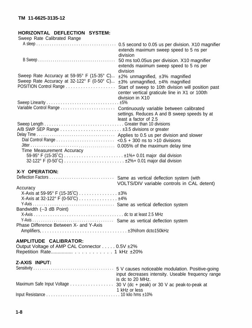
HORIZONTAL DEFLECTION SYSTEM:Sweep Rate Calibrated Range
A sleep . . . . . . . . . . . . . . . . . . . . . . . . . . . . . . . . . . . . 0.5 second to 0.05 us per division. X10 magnifierextends maximum sweep speed to 5 ns perdivision
B Sweep . . . . . . . . . . . . . . . . . . . . . . . . . . . . . . . . . . . . . 50 ms to0.05us per division. X10 magnifierextends maximum sweep speed to 5 ns perdivision
Sweep Rate Accuracy at 59-95° F (15-35° C)... ±2% unmagnified, ±3% magnifiedSweep Rate Accuracy at 32-122° F (0-50° C)... ±3% unmagnified, ±4% magnifiedPOSITION Control Range . . . . . . . . . . . . . . . . . . . . Start of sweep to 10th division will position past
center vertical graticule line in X1 or 100thdivision in X10
Sweep Linearity . . . . . . . . . . . . . . . . . . . . . . . . . . . . . . . ±5%Variable Control Range . . . . . . . . . . . . . . . . . . . . . . . Continuously variable between calibrated
settings. Reduces A and B sweep speeds by atleast a factor of 2.5
Sweep Length . . . . . . . . . . . . . . . . . . . . . . . . . . . . . . . . . Greater than 10 divisionsA/B SWP SEP Range . . . . . . . . . . . . . . . . . . . . . . . . ±3.5 divisions or greaterDelay Time . . . . . . . . . . . . . . . . . . . . . . . . . . . . . . . . . . . . Applies to 0.5 us per division and slower
Dial Control Range . . . . . . . . . . . . . . . . . . . . . . . . . <0.5 + 300 ns to >10 divisionsJitter . . . . . . . . . . . . . . . . . . . . . . . . . . . . . . . . . . . . . . . . 0.005% of the maximum delay timeTime Measurement Accuracy
59-95° F (15-350 C) . . . . . . . . . . . . . . . . . . . . . . . . ±1%+ 0.01 major dial division32-122° F (0-500 C) . . . . . . . . . . . . . . . . . . . . . . . . ±2%+ 0.01 major dial division
X-Y OPERATION:Deflection Factors . . . . . . . . . . . . . . . . . . . . . . . . . . . . . Same as vertical deflection system (with
VOLTS/DIV variable controls in CAL detent)Accuracy
X-Axis at 59-95° F (15-350C) . . . . . . . . . . . . . . . ±3%X-Axis at 32-122° F (0-500C) . . . . . . . . . . . . . . . ±4%Y-Axis . . . . . . . . . . . . . . . . . . . . . . . . . . . . . . . . . . . . . . Same as vertical deflection system
Bandwidth (--3 dB Point)X-Axis . . . . . . . . . . . . . . . . . . . . . . . . . . . . . . . . . . . . . . dc to at least 2.5 MHzY-Axis . . . . . . . . . . . . . . . . . . . . . . . . . . . . . . . . . . . . . . Same as vertical deflection system
Phase Difference Between X- and Y-AxisAmplifiers, . . . . . . . . . . . . . . . . . . . . . . . . . . . . . . . . . . ±3%from dcto150kHz
AMPLITUDE CALIBRATOR:Output Voltage of AMP CAL Connector . . . . . 0.5V ±2%Repetition Rate................ . . . . . . . . . . . 1 kHz ±20%
Z-AXIS INPUT:Sensitivity . . . . . . . . . . . . . . . . . . . . . . . . . . . . . . . . . . . . . 5 V causes noticeable modulation. Positive-going
input decreases intensity. Useable frequency rangeis dc to 20 MHz.
Maximum Safe Input Voltage . . . . . . . . . . . . . . . . . 30 V (dc + peak) or 30 V ac peak-to-peak at1 kHz or less
Input Resistance . . . . . . . . . . . . . . . . . . . . . . . . . . . . . . . 10 kilo hms ±10%
1-8

TM 11-6625-3135-12
POWER SOURCE:Line Voltage Ranges . . . . . . . . . . . . . . . . . . . . . . . . . .Line Frequency . . . . . . . . . . . . . . . . . . . . . . . . . . . . . . . .Maximum Power Consumption . . . . . . . . . . . . . . .Line Fuse . . . . . . . . . . . . . . . . . . . . . . . . . . . . . . . . . . . . . .
CATHODE RAY TUBE:Display Area . . . . . . . . . . . . . . . . . . . . . . . . . . . . . . . . . .Standard Phosphor . . . . . . . . . . . . . . . . . . . . . . . . . . .Nominal Accelerating Voltage . . . . . . . . . . . . . . . . .
ENVIRONMENTAL CHARACTERISTICS:Operating Temperature . . . . . . . . . . . . . . . . . . . . . . .Nonoperating Temperature . . . . . . . . . . . . . . . . . . .Operating Altitude . . . . . . . . . . . . . . . . . . . . . . . . . . . .
Nonoperating Altitude . . . . . . . . . . . . . . . . . . . . . . . .Operating Humidity . . . . . . . . . . . . . . . . . . . . ... . . .Nonoperating Humidity . . . . . . . . . . . . . . . . . . . . . . .Vibration (Operating) . . . . . . . . . . . . . . . . . . . . . . . . .
Electromagnetic Interference . . . . . . . . . . . . . . . . . .
PHYSICAL CHARACTERISTICS:Weight with Accessories . . . . . . . . . . . . . . . . . . . . . . .Weight without Accessories . . . . . . . . . . . . . . . . . . .Domestic Shipping Weight . . . . . . . . . . . . . . . . . . . .Height with Empty Pouch . . . . . . . . . . . . . . . . . . . . .Height without Pouch . . . . . . . . . . . . . . . . . . . . . . . . .Width with Handle . . . . . . . . . . . . . . . . . . . . . . . . . . . .Width without Handle . . . . . . . . . . . . . . . . . . . . . . . .Length with Front Cover . . . . . . . . . . . . . . . . . . . . . .Length without Front Cover.. . . . . . . . . . . . . . . . .Length with Handle Extended . . . . . . . . . . . . . . . . .
90 V ac to 250 V ac48 to 440 Hz40 W (70 VA)1.0 A, 250 V, Slow-blow
80mmx100mmP3114 kV
32-122° F (0-50° C)-67 to +167°F (--55 to + 75°C)Up to 15,000 ft (4,500m). Maximum temperaturedecreased 1° C per 1,000 ft above 5,000 ftTo 50,000 ft (15,000 m)95% at 86-122° F (30-50° C)95% at 86-140° F (30-60° C)Can withstand total displacement of 0.01 5 inchp-p (2.4 g’s at 55 Hz) along all three axes, withfrequency varied from 10 Hz to 55 Hz, for periodof 15 minutesMeets requirements of MIL STD-461B Pt 4
20.0 lb (9.1 kg)13.5 lb (6.1 kg)24.1 lb (10.9 kg)5.9 in. (150 mm)5.4 in. (137 mm)14.2 in. (360 mm)12.9 in. (328 mm)17.5 in. (445 mm)17.3 in. (440 mm)20.1 in. (511 mm)
1-9

TM 11-6625-3135-12
Section Ill. TECHNICAL PRINCIPLES OF OPERATION
1-14. FUNCTIONAL DESCRIPTION
The following is a basic functional description of the oscilloscope. Refer to fig. 1-2 for a blockdiagram.
There are two vertical attenuators (one for each channel). The attenuator circuits providecontrol of input coupling, vertical deflection factor, and variable volts-per-division gain. Aninvert circuit in the channel 2 attenuator allows you to invert the channel 2 input signal.
The vertical preamp and output circuit amplifies the input signals. This makes the signal levelhigh enough for vertical deflection of the electron beam in the crt. The dynamic range of theamplifier can be limited with the beam find switch. The amplifier also intensifies the trace andlimits horizontal deflection.
The A sweep generator and logic circuit produces a linear voltage ramp for horizontaldeflection of the crt beam. The sweep generator also produces signals that generate correcttiming of the crt unblinking and intensity levels.
The A trigger circuitry uses either an internal signal, external trigger, or ac line trigger signal todevelop a gate signal for the A sweep generator. The B trigger circuitry uses only the internaltrigger signal to gate the B signal generator.
The alternate B sweep circuitry produces a linear voltage ramp that is amplified by thehorizontal amplifier. This provides the B sweep horizontal deflection on the crt. The alternateB sweep circuitry also produces sweep-switching signals that control the display of the A andB sweeps, and gate signals used to establish the crt unblinking and intensity levels for the Aintensified and B sweep displays.
The X-Y amplifier amplifies the channel 1 signal from the internal circuit and applies it to thehorizontal amplifier. The horizontal amplifier provides output signals to drive the crthorizontal deflection plates.
The power supply converts ac power-line voltage into voltages needed for oscilloscopeoperation. The Z-axis amplifier uses several input signal sources to control the crt intensitylevel.
The crt provides a visual display of the electrical properties of the circuit or signal underexamination.
1-10

TM 11-6625-3135-12
Figure 1-2. AN/USM-488 Oscilloscope Block Diagram
1-11/(1-12 Blank)


TM 11-6625-3135-12
CHAPTER 2OPERATING INSTRUCTIONS
Para Page
General Operator Preventive Maintenance Checks and Services . . . . . . . . .Operating Procedures . . . . . . . . . . . . . . . . . . . . . . . . . . . . . . . . . . . . . . . . . . . . . . . . . . . . . . Operation in Unusual Weather . . . . . . . . . . . . . . . . . . . . . . . . . . . . . . . . . . . . . . . . . . . . .PMCS Table . . . . . . . . . . . . . . . . . . . . . . . . . . . . . . . . . . . . . . . . . . . . . . . . . . . . . . . . . . . . . . .
2-12-32-42-2
2-82-112-442-8
2-1

TM 11-6625-3135-12
Section I. DESCRIPTION AND USE OF OPERATOR’S CONTROLSAND INDICATORS
Key Control Or Indicator Function
1
2
3
4
5
6
7
8
9
2-2
Cathode Ray Tube
A INTENSITYControl
B INTENSITYControl
TRACE ROTATIONControl
BEAM FIND Switch
SCALE ILLUMControl
FOCUS Control
POWER Switch
POWER Indicator
Provides visual display of electrical properties of circuitunder examination
Controls brightness of A sweep trace
Controls brightness of B sweep trace
Screwdriver adjustment used to align trace with horizontalgraticule line
When held depressed, compresses display to within graticulearea to aid in locating off-screen displays
Adjusts brightness of graticule illumination
Adjusts for optimum display definition
Turns oscilloscope power on and off
When illuminated, indicates power applied to oscilloscope
TM 11-6625-3135-12
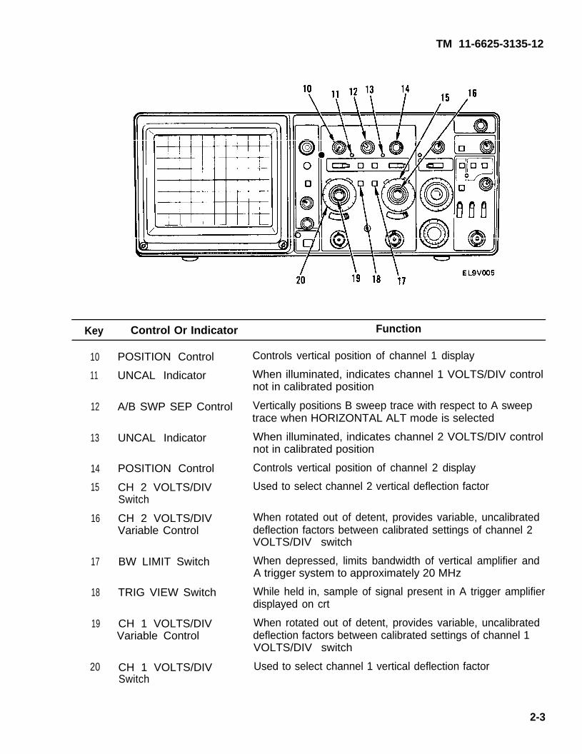
Key Control Or Indicator Function
10
11
12
13
14
15
16
17
18
19
20
POSITION Control
UNCAL Indicator
A/B SWP SEP Control
UNCAL Indicator
POSITION Control
CH 2 VOLTS/DIVSwitch
CH 2 VOLTS/DIVVariable Control
BW LIMIT Switch
TRIG VIEW Switch
CH 1 VOLTS/DIVVariable Control
CH 1 VOLTS/DIVSwitch
Controls vertical position of channel 1 display
When illuminated, indicates channel 1 VOLTS/DIV controlnot in calibrated position
Vertically positions B sweep trace with respect to A sweeptrace when HORIZONTAL ALT mode is selected
When illuminated, indicates channel 2 VOLTS/DIV controlnot in calibrated position
Controls vertical position of channel 2 display
Used to select channel 2 vertical deflection factor
When rotated out of detent, provides variable, uncalibrateddeflection factors between calibrated settings of channel 2VOLTS/DIV switch
When depressed, limits bandwidth of vertical amplifier andA trigger system to approximately 20 MHz
While held in, sample of signal present in A trigger amplifierdisplayed on crt
When rotated out of detent, provides variable, uncalibrateddeflection factors between calibrated settings of channel 1VOLTS/DIV switch
Used to select channel 1 vertical deflection factor
2-3

TM 11-6625-3135-12
Key Control Or Indicator Function
21 VERTICAL MODECH 1/BOTH/CHSwitch
22 CH 1 TRIGGERSOURCE Switch
22-23 COMPOSITE
2
23
24
25
26
CH 2 TRIGGERSOURCE Switch
VERTICAL MODEADD/ALT/CHOPSwitch
AC/GND/DC Switch
AC/GND/DC Switch
When set to CH 1, selects only channel 1 input signalfor display. When set to BOTH, selects both channel 1and channel 2 input signals for display. When set to CH 2,selects only channel 2 input signal for display
When depressed, selects signal applied to CH 1 OR XINPUT connector as trigger source
When CH 1 and CH 2 switches are either both depressed orboth released, composite trigger source is selected, Triggersource is then determined by signals selected for display bythe VERTICAL MODE switches
When depressed, selects signal applied to CH 2 OR YINPUT connector as trigger source
When set to ADD, displays algebraic sum of channel 1and channel 2 input signals. When set to ALT, displayschannel 1 and channel 2 input signals alternately at end ofeach trace. When set to CHOP, displays channel 1 andchannel 2 input signals alternately during sweep time
Three-position switch to select method of coupling inputsignal to channel 2 deflection system. It also establishes DCground reference line on crt.
Three-position switch to select method of coupling inputsignal to channel 1 deflection system. It also establishes DCground reference line on crt.
2-4

TM 11-6625-3135-12
Key Control Or Indicator Function
27
28
29
30A
30B
31
32
UNCAL Indicator
POSITION Control
HORIZONTAL MODEA/ALT/B Switch
A SEC/DIV Switch
B SEC/DIV Switch
SEC/DIV VariableControl and X10Multiplier Switch
B DELAY TIMEPOSITION Control
When illuminated, indicates SEC/DIV variable control isnot in calibrated position
Moves A sweep and B sweep displays horizontally andhorizontally positions X-axis in X-Y mode of operation
Determines mode of operation for horizontal deflectionsystem. When set to A, horizontal deflection is provided byA sweep generator. When set to ALT, display alternatesbetween A sweep and B delayed sweep. When set to B,horizontal deflection is provided by B sweep generator
Used to select sweep speeds for A and B sweep generators ina 1, 2, 5 sequence. To lock A and B sweeps together, pull theB SEC/DIV switch out and align the pointer on the BSEC/DIV switch between the two markers on the ASEC/DIV switch, then release the switch. If the twoswitches are not locked together, B sweep can be delayed.Setting A SEC/DIV switch to X-Y locks the A sweep inhorizontal mode.
Provides continuously variable, uncalibrated sweep speeds.Pulling control out actuates X 10 magnifier switch, whichexpands crt display by a factor of 10
Selects amount of delay time between start of A sweep andstart of B sweep. Delay time is variable from 0.5 to 10 timesA SEC/DIV switch setting
2-5

TM 11-6625-3135-12
Key Control Or Indicator Function
33
34
35
35-36
36
37
38
39
VAR HOLDOFFControl
B TRIGGER LEVELControl
A TRIGGER NORMSwitch
TV FIELD
A TRIGGERP-P AUTO/TV LINESwitch
A TRIGGER SGL SWPRESET Switch
A TRIGGER LEVELControl
A EXTSwitch
COUPLING
Provides continuous control of hold off time between sweepsand increases hold off time by at least a factor of 10
Selects amplitude pointtriggered
When depressed,signal is applied
sweep
on trigger signal at which B sweep is
is initiated when adequate trigger
Depressing both P-Ppermits triggering on
AUTO and NORM pushbuttonstelevision field signals
Permits triggering on waveforms and television lines havingrepetition rate of at least 20 Hz. Sweep free-runs in absenceof adequate trigger signal
When momentarily depressed, arms A trigger circuit forsingle-sweep display
Selects amplitude point on trigger signal at which A sweep istriggered
Three-position switch that determines method used tocouple external signals from EXT INPUT connector to Atrigger circuit
2-6

TM11-6625-3135-12
Key Control Or Indicator Function
40 B TRIGGER SLOPE Selects slope of signal that triggers B channel sweepSwitch
41 TRIG’D/READYIndicator
42 A TRIGGER SLOPESwitch
43 A SOURCE Switch
44 A TRIG BW Switch
Illuminates when either P-P AUTO or NORM trigger modeis selected
Selects slope of signal that triggers A channel sweep
Three-position switch that determines source of triggersignal coupled to input of A trigger circuit. When set toINT, permits triggering on signal applied to CH 1 OR Xconnector or CH 2 OR Y connector. When set to LINE,selects ac line voltage as trigger signal. When set to EXT,permits triggering on signals applied to EXT INPUTconnector
Three-position switch that selects trigger bandpassfrequencies for A trigger circuit. When set to FULL, allowsall frequency components to pass. When set to HF REJ,attenuates all trigger signals above approximately 40 kHz.When set to LF REJ, attenuates all trigger signals belowapproximately 40 kHz
2-7

TM 11-6625-3135-12
Section Il. OPERATOR PREVENTIVE MAINTENANCE CHECKSAND SERVICES (PMCS)
2-1. GENERAL
Operator Preventive Maintenance Checks and Services (PMCS) is the required inspection and careof your equipment necessary to keep it in good operating condition.
a. Before You Operate. Always keep in mind the CAUTIONS and WARNINGS. Perform yourbefore - PMCS.
b. While YOU Operate. Always keep in mind the CAUTIONS and WARNINGS. Perform yourduring - PMCS.
c. After YOU Operate. Be sure to perform your after-operation PMCS.
d. If Your Equipment Falls to Operate. Troubleshoot with proper equipment. Report anydeficiencies using the proper forms. See DA PAM 738-750.
2-2. PMCS TABLE
The PMCS are shown in table 2-1.
a. Item Number Column. The numbers appearing in this column are in the order the workshould be performed. The numbers are keyed to fig. 2-1 to identify work locations. This column shallalso be used as a source of item numbers for the TM Number Column on DA Form 2404 (EquipmentInspection and Maintenance Worksheet) in recording results of PMCS.
b. Interval Column. This column indicates whether PMCS are performed before operation (B),during operation (D), after operation (A), or weekly (W).
c. Item to be Inspected Column. This column identifies the item to be inspected.
d. Procedures Column. This column contains a brief description of the check or service to beperformed and step-by-step procedures.
e. Equipment is Not Ready If Column. This column identifies the condition that prevents theequipment from being ready for operation.
2-8
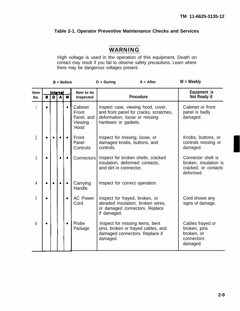
ItemNo.
1
2
3
4
5
6
TM 11-6625-3135-12
Table 2-1. Operator Preventive Maintenance Checks and Services
WARNINGHigh voltage is used in the operation of this equipment. Death oncontact may result if you fail to observe safety precautions. Learn wherethere may be dangerous voltages present.
B = Before D = During A = After
Item to beInspected
CabinetFrontPanel, andViewing‘Hood
FrontPanelControls
Connectors
CarryingHandle
AC PowerCord
ProbePackage
Procedure
Inspect case, viewing hood, cover,and front panel for cracks, scratches,deformation, loose or missinghardware or gaskets.
Inspect for missing, loose, ordamaged knobs, buttons, andcontrols.
Inspect for broken shells, crackedinsulation, deformed contacts,and dirt in connector.
Inspect for correct operation.
Inspect for frayed, broken, orabraded insulation, broken wires,or damaged connectors. Replaceif damaged.
Inspect for missing items, bentpins, broken or frayed cables, anddamaged connectors. Replace ifdamaged.
W = Weekly
Equipment isNot Ready if:
Cabinet or frontpanel is badlydamaged.
Knobs, buttons, orcontrols missing ordamaged.
Connector shell isbroken, insulation iscracked, or contactsdeformed.
Cord shows anysigns of damage.
Cables frayed orbroken, pinsbroken, orconnectorsdamaged.
2-9

TM 11-6625-3135-12
Figure 2-1. Oscilloscope PMCS Location Diagram
2-10
TM 11-6625-3135-12
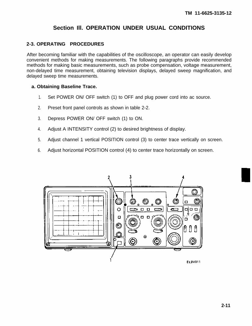
Section Ill. OPERATION UNDER USUAL CONDITIONS
2-3. OPERATING PROCEDURES
After becoming familiar with the capabilities of the oscilloscope, an operator can easily developconvenient methods for making measurements. The following paragraphs provide recommendedmethods for making basic measurements, such as probe compensation, voltage measurement,non-delayed time measurement, obtaining television displays, delayed sweep magnification, anddelayed sweep time measurements.
a. Obtaining Baseline Trace.
1.
2.
3.
4.
5.
6.
Set POWER ON/ OFF switch (1) to OFF and plug power cord into ac source.
Preset front panel controls as shown in table 2-2.
Depress POWER ON/ OFF switch (1) to ON.
Adjust A INTENSITY control (2) to desired brightness of display.
Adjust channel 1 vertical POSITION control (3) to center trace vertically on screen.
Adjust horizontal POSITION control (4) to center trace horizontally on screen.
2-11

TM 11-6625-3135-12
Table 2-2. Controls, Preset Positions
Control
Display
A AND B INTENSITYFOCUS
Vertical (Both Channels)
POSITIONPOSITION and INVERT (Channel 2 only)VERTICAL MODE CH 1/BOTH/CH 2TRIGGER SOURCEBW LIMITVOLTS/DIV SwitchVOLTS/DIV Variable ControlAC/GND/DC
Horizontal
B
A/B SWP SEPPOSITIONMODEA AND B SEC/DIV SwitchSEC/DIV Variable ControlX10 MultiplierB DELAY TIME POSITION
Trigger
SLOPELEVEL
A TriggerVAR HOLDOFFTRIGGER MODE P-P AUTO/TV LINESLOPELEVELA TRIG BWA SOURCEA EXT COUPLING
Position
Fully counterclockwiseMidrange
MidrangeMidrange and pushed inCH 1COMPOSITE (both in or both out)Off (button out)50 mVCAL detentAC
MidrangeMidrangeA0.5 msCAL detentOff (knob in)Fully counterclockwise
outFully clockwise
NORMInoutMidrangeFULLINTAC
2-12

TM 11-6625-3135-12
b. Probe Compensation.
1.
2.
3.
4.
5.
6.
7.
8.
9.
NOTE
Misadjustment of probe compensation is a common source of meas-urement error. To ensure optimum measurement accuracy, alwayscompensate the oscilloscope probes before making measurements.
Obtain baseline trace as described in para 2-3a.
Connect one 10X probe to CH 1 OR X connector (1) and one 10X probe to CH 2 OR Yconnector (2).
Set both CH 1 and CH 2 VOLTS/DIV switches (3 and 4) to 0.1 10X PROBE.
Set both AC/GND/DC switches (5 and 6) to DC.
Set VERTICAL MODE CH 1/BOTH/CH 2 switch (7) to CH 1.
Insert tip of channel 1 probe into AMP CAL connector (8) and adjust CH 1 VOLTS/DIVvariable control (9) to obtain display amplitude of five vertical divisions.
Set A SEC/DIV switch (10) to display 5 cycles of AMP CAL signal.
Using channel 1 vertical POSITION control (11), vertically center display on crt screen.
Using low-reactance alignment tool, adjust low-frequency compensation control on probecompensation box to obtain best wave orm with flattest top.
2-13

TM 11-6625-3135-12
2-14
10. Set VERTICAL MODE CH 1/BOTH/CH 2 switch (7) to CH2.
11. Insert tip of channel 2 probe into AMP CAL connector and adjust CH 2 VOLTS/DIVvariable control (12) to obtain display amplitude of five vertical divisions.
12. Set A SEC/DIV switch (10) to display five cycles of AMP CAL signal.
13. Using channel 2 vertical POSITION control (13), vertically center disp
14. Using low-reactance alignment tool, adjust low-frequency compensationcompensation box to obtain best waveform with flattest top.
15. Probes are now properly compensated.
lay on crt screen.
control on probe

TM11-6625-3135-12
C. Peak-To-Peak Voltage Measurements.
1. Obtain baseline trace as described in para 2-3a.
2. Apply ac signal to either CH 1 OR X connector (1) or CH 2 OR Y connector (2) and setVERTICAL MODE CH 1/BOTH/CH 2 switch (3) to display channel used.
3. Set CH 1 or CH 2 VOLTS/DIV variable control (4 or 5) for appropriate channel to CALdetent position, and set appropriate VOLTS/DIV switch (6 or 7) to display about fivevertical divisions of waveform.
4. Adjust A TRIGGER LEVEL control (8) to obtain stable display.
5. Set A SEC/DIV switch (9) to position that allows several cycles of waveform to bedisplayed.
6. Rotate appropriate vertical POSITION control (10 or 11) until waveform negative peakcoincides with one horizontal graticule line.
7. Rotate horizontal POSITION control (12) until one positive peak coincides with centervertical graticule line.
2-15

TM 11-6625-3135-12
8. Measure deflection from negative point A to positive point B.
N O T E
If amplitude measurement is critical or trace is thick because of noise orhum on the signal, a more accurate value can be obtained by measuringfrom the top of the peak to the top of the valley. This eliminates tracethickness from the measurement.
9. Calculate the voltage, using the following formula:
vertical VOLTS/DIV switch setting indicatedvolts (p-p) = deflection x 1X (or 10X PROBE when 10X probe is
(divisions) used)
EXAMPLE: Measured peak-to-peak vertical deflection is 4.6 divisions, a 10X attenuatorprobe is used and VOLTS/DIV switch is set to 5 at the 10X PROBE setting. Substitutingthe given values:
volts (p-p) = 4.6 div x 5 volts/div = 23 volts
2-16
TM 11-6625-3135-12
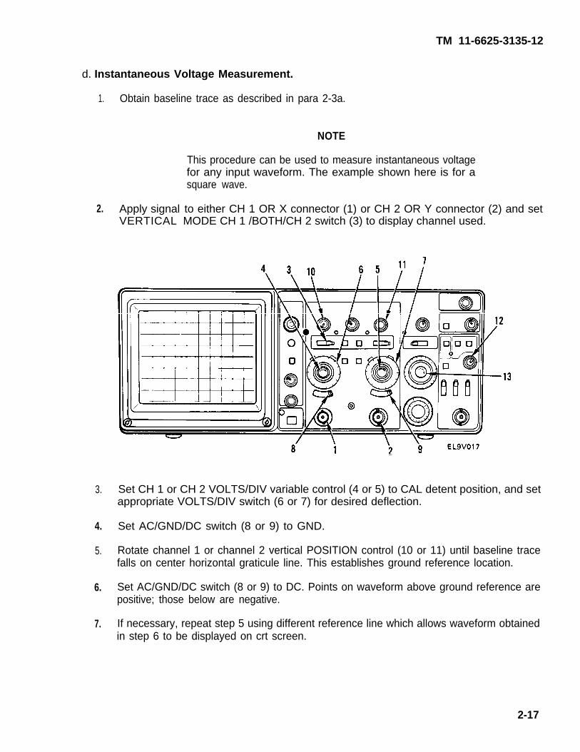
d. Instantaneous Voltage Measurement.
1. Obtain baseline trace as described in para 2-3a.
2. Apply signalVERTICAL
NOTE
This procedure can be used to measure instantaneous voltagefor any input waveform. The example shown here is for asquare wave.
to either CH 1 OR X connector (1) or CH 2 OR Y connector (2) and setMODE CH 1 /BOTH/CH 2 switch (3) to display channel used.
3. Set CH 1 or CH 2 VOLTS/DIV variable control (4 or 5) to CAL detent position, and setappropriate VOLTS/DIV switch (6 or 7) for desired deflection.
4. Set AC/GND/DC switch (8 or 9) to GND.
5. Rotate channel 1 or channel 2 vertical POSITION control (10 or 11) until baseline tracefalls on center horizontal graticule line. This establishes ground reference location.
6. Set AC/GND/DC switch (8 or 9) to DC. Points on waveform above ground reference arepositive; those below are negative.
7. If necessary, repeat step 5 using different reference line which allows waveform obtainedin step 6 to be displayed on crt screen.
2-17

TM 11-6625-3135-12
8.
9.
10.
11.
12.
If using channel 2, ensure that channel 2 vertical POSITION control (11) is pushed in.
Adjust A TRIGGER LEVEL control (12) to obtain stable display.
Set A SEC/DIV switch (13) to position that allows several cycles of waveform to bedisplayed.
Count number of divisions of vertical deflection between ground reference line and pointon waveform at which voltage level is to be determined.
Calculate voltage using formula:
Verticalinstantaneous = deflection x polarity xvoltage (divisions) (+ or --)
VOLTS/DIV switch setting indicatedby 1X (or 10X PROBE when 10X probeis used)
EXAMPLE: Vertical deflection from reference line is 4.6 divisions. The waveform point isabove the reference line, a 10X attenuator probe is used, and VOLTS/ DIV switch is set to 2at the 10X PROBE position. Substituting given values:
instantaneous voltage = 4.6 div x (+1) x 2 volts/div = +9.2 volts
2-18
TM 11-6625-3135-12
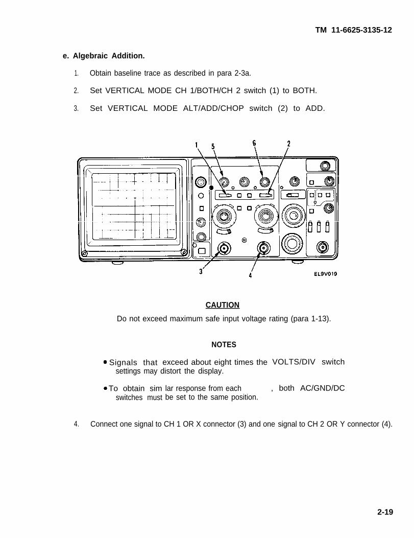
e. Algebraic Addition.
1. Obtain baseline trace as described in para 2-3a.
2. Set VERTICAL MODE CH 1/BOTH/CH 2 switch (1) to BOTH.
3. Set VERTICAL MODE ALT/ADD/CHOP switch (2) to ADD.
CAUTION
Do not exceed maximum safe input voltage rating (para 1-13).
Signals thatsettings may
NOTES
exceed about eight times thedistort the display.
To obtain simswitches must
VOLTS/DIV switch
lar response from each , both AC/GND/DCbe set to the same position.
4. Connect one signal to CH 1 OR X connector (3) and one signal to CH 2 OR Y connector (4).
2-19

TM 11-6625-3135-12
5. Set VERTICAL MODE CH 1/BOTH/CH 2 switch (1) to CH 1 and adjust channel 1vertical POSITION control (5) to center display vertically on crt screen.
6. Set VERTICAL MODE CH 1/BOTH CH 2 switch (1) to CH 2 and adjust channel 2vertical POSITION control (6) to center display vertically on crt screen.
7. Set VERTICAL MODE CH 1/BOTH/CH 2 switch (1) to BOTH.
NOTES
If the channel 2 vertical POSITION control is pushed in, theresultant waveform is the sum of the two applied signals.
If the channel 2 vertical POSITION control is pulled out, theresultant waveform is the difference between the two signals.
2-20

TM 11-6625-3135-12
f. Common-Mode Rejection.
1.
2.
3.
4.
5.
6.
7.
Obtain baseline trace as described in para 2-3a.
NOTE
This procedure can be used to measure instantaneous voltage for anyinput waveform. The example shown here is for a square wave.
Connect signal containing unwanted line-frequency components to CH 1 OR X connector (1).
Connect line-frequency signal to CH 2 OR Y connector (2).
Set
Set
Set
NOTE
For maximum cancellation, the signal connected to channel 2 must bein phase with the unwanted line-frequency component connected tochannel 1.
VERTICAL MODE CH 1/BOTH/CH 2 switch (3) to BOTH.
VERTICAL MODE ADD/ALT/CHOP switch (4) to ALT.
both CH 1 and CH 2 VOLTS/DIV switches (5 and 6) to produce displays four or fivedivisions in amplitude.
Adjust either CH 1 or CH 2 VOLTS/DIV switch (5 or 6) and appropriate VOLTS/DIVvariable control (7 or 8) so that both displays are of equal amplitude.
2-21

TM 11-6625-3135-12
8.
9.
10.
11.
Adjust CH 2 VOLTS/DIV switch (6) and CH 2 VOLTS/DIV variable control (8) so thatchannel 2 display amplitude is approximately same amplitude as undesired portion ofchannel 1 display.
Set VERTICAL MODE ADD/ALT/CHOP switch (4) to ADD.
Pull out channel 2 vertical POSITION control (9) to invert signal.
Slightly readjust CH 2 VOLTS/DIV variable control (8) for maximum cancellation ofunwanted signal.
2-22
TM 11-6625-3135-12
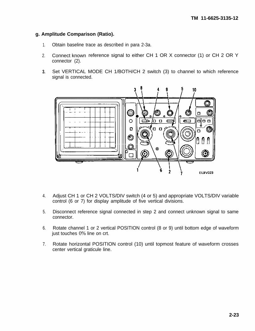
g. Amplitude Comparison (Ratio).
1. Obtain baseline trace as described in para 2-3a.
2. Connect knownconnector (2).
reference signal to either CH 1 OR X connector (1) or CH 2 OR Y
3. Set VERTICAL MODE CH 1/BOTH/CH 2 switch (3) to channel to which referencesignal is connected.
4. Adjust CH 1 or CH 2 VOLTS/DIV switch (4 or 5) and appropriate VOLTS/DIV variablecontrol (6 or 7) for display amplitude of five vertical divisions.
5. Disconnect reference signal connected in step 2 and connect unknown signal to sameconnector.
6. Rotate channel 1 or 2 vertical POSITION control (8 or 9) until bottom edge of waveformjust touches 0% line on crt.
7. Rotate horizontal POSITION control (10) until topmost feature of waveform crossescenter vertical graticule line.
2-23

TM 11-6625-3135-12
8. Read percent ratio directly from graduations of center vertical graticule line, referring to0% and 100% marks on left edge of graticule. (One minor division equals 4% for five-division display.)
2-24

TM 11-6625-3135-12
h. Time Duration Measurement.
1. Obtain baseline trace as described in para 2-3a.
NOTE
This procedure can be used to measure instantaneous voltage for anyinput waveform. The example shown here is for a square wave.
2. Connect signal to either CH 1 OR X connector (1) or CH 2 OR Y connector (2).
3. Set VERTICAL MODE CH 1/BOTH/CH 2 switch (3) to appropriate channel.
4. Adjust A TRIGGER LEVEL control (4) to obtain stable display.
5. Set A and B SEC/DIV variable control (5) to CAL detent, and set A SEC/DIV switch (6)to display one complete cycle of waveform.
6. Rotate channel 1 or channel 2 vertical POSITION control (7 or 8) until time measurementpoints fall on center horizontal graticule.
7. Count horizontal divisions between time measurement points.
2-25
TM 11-6625-3135-12
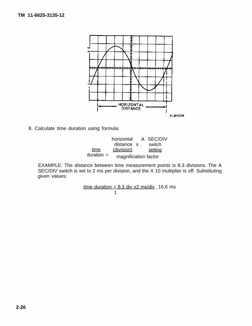
8. Calculate time duration using formula:
horizontal A SEC/DIVdistance x switch
time (division) settingduration = magnification factor
EXAMPLE: The distance between time measurement points is 8.3 divisions. The ASEC/DIV switch is set to 2 ms per division, and the X 10 multiplier is off. Substitutinggiven values:
time duration = 8.3 div x2 ms/div = 16.6 ms1
2-26

TM 11~6625-3135-12
i. Frequency Measurement.
1.
2.
j. Rise
1.
2.
3.
4.
5.
Measure time duration of one cycle of waveform as described in paragraph 2-3h.
Calculate reciprocal of time duration determined in step 2-3h(8) to determine frequency ofwaveform.
EXAMPLE: The signal obtained has a time duration of 16.6 ms. Substituting given values:
frequency =1 = 1
q 60 Hztime duration 16.6 ms
Time Measurement.
Obtain baseline trace as described in paragraph 2-3a.
Set BW LIMIT switch (1) to off (pushbutton out).
Connect signal to either CH 1 OR X connector (2) or CH 2 OR Y connector (3).
Set VERTICAL MODE CH 1/BOTH/CH 2 switch (4) to appropriate channel.
Set appropriate CH 1 or CH 2 VOLTS/DIV switch (5 or 6) and VOLTS/DIV variablecontrol (7 or 8) for an exact five-division display.
2-27
TM 11-6625-3135-12
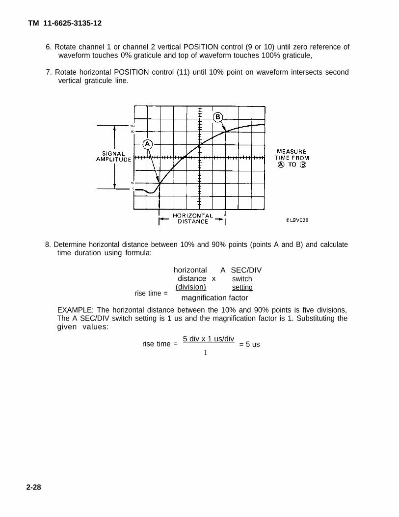
6. Rotate channel 1 or channel 2 vertical POSITION control (9 or 10) until zero reference ofwaveform touches 0% graticule and top of waveform touches 100% graticule,
7. Rotate horizontal POSITION control (11) until 10% point on waveform intersects secondvertical graticule line.
8. Determine horizontal distance between 10% and 90% points (points A and B) and calculatetime duration using formula:
horizontal A SEC/DIVdistance x switch
(division) settingrise time =
magnification factor
EXAMPLE: The horizontal distance between the 10% and 90% points is five divisions,The A SEC/DIV switch setting is 1 us and the magnification factor is 1. Substituting thegiven values:
5 div x 1 us/divrise time = = 5 us
1
2-28

TM 11-6625-3135-12
k. Rise Time Measurement in Delayed-Sweep Mode.
1.
2.
3.
4.
5.
6.
7.
8.
Obtain baseline trace as described in para 2-3a.
Connect signal to either CH 1 OR X connector (1) or CH 2 OR Y connector (2).
Set VERTICAL MODE CH 1 /BOTH/CH 2 switch (3) to selected channel.
Set appropriate CH 1 or CH 2 VOLTS/DIV switch (4 or 5) and VOLTS, DIV variablecontrol (6 or 7) to provide display amplitude of exactly five divisions.
Rotate appropriate channel 1 or 2 vertical POSITION control (8 or 9) until zero referenceline of waveform touches 0% graticule line and top of waveform touches 100% graticuleline.
Set SEC/DIV variable control (10) to CAL detent position and set A SEC/DIV switch(11) so one rise time of interest is displayed.
Set HORIZONTAL MODE switch (12) to ALT.
Adjust B DELAY TIME POSITION control (13) to intensify rise time of interest on Atrace.
2-29

TM 11-6625-3135-12
9.
10.
11.
12.
13.
Set B SEC/DIV switch (11) so portion of A trace being measured is spread as much aspossible on B sweep.
Set HORIZONTAL MODE switch (12) to B.
Adjust B DELAY TIME POSITION control (13) until display intersects 10% point atcenter vertical graticule line. Record B DELAY TIME POSITION control dial reading.
THE 10% POINT ON THE WAVEFORM INTERSECTS THE 90% POINT ON THE WAVEFORM INTERSECTSTHE CENTER VERTICAL GRATICULE LINE. THE CENTER VERTICAL GRATICULE LINE.
EL9V043
Adjust B DELAY TIME POSITION control (13) until display intersects the 90% point at center vertical graticule line. Record B DELAY TIME POSITION control dial reading.
Calculate rise time using the formula:
time second first A SEC/DIVdifference = dial – dial x switch(duration) setting setting setting
EXAMPLE: A SEC/ DIV switch is set to 1 us per division, first B DELAY TIMEPOSITION control is set to 2.50, and second B DELAY TIME POSITION control is setto 7.50. Substituting given values:
rise time =(7.03 - 2.50)(1 us/div) = 5 us\ /. /
2-30

TM 11-6625-3135-12
1. Phase Difference Measurement.
1. Obtain baseline trace as described in para 2-3a.
2. Depress CH 1 TRIGGER SOURCE switch (1).
3. Set both AC/GND/DC switches (2 and 3) to desired positions and ensure that both are setto same position.
4. Using either probes or cables with equal time delays, connect known reference signal to CH1 OR X connector (4) and comparison signal to CH 2 OR Y connector (5).
5. Set both CH 1 and CH 2 VOLTS/DIV switches (6 and 7) for four- or five-division display.
6. Set VERTICAL MODE CH 1/BOTH/CH 2 switch (8) to BOTH.
7. Set VERTICAL MODE ADD/ALT/CHOP switch (9) to either ALT or CHOP,depending on frequency of input signals.
NOTE
The reference signal should precede the comparison signal in time.
8. If two signals are opposite polarities, pull out channel 2 vertical POSITION control (10) toinvert channel 2 display.
2-31

TM11-6625-3135-12
9.
10.
11.
12.
13.
14.
Adjust both CH 1 and CH 2 VOLTS/DIV variable controls (1 1 and 12) until two displaysare equal in amplitude.
Adjust A TRIGGER LEVEL control (13) for stable display.
Set A SEC/DIV switch (14) to sweep speed setting which provides display of one full cycleof reference signal.
Using horizontal POSITION control (15), center display.
Adjust SEC/DIV variable control (16) until one reference signal cycle occupies exactlyeight horizontal graticule divisions at 50% rise-time points. Each graticule division nowrepresents 45° and graticule calibration can be stated as 45° per division.
Determine horizontal difference between corresponding points on waveforms at commonhorizontal graticule line and calculate phase difference using formula:
horizontal horizontalphase difference = difference x calibration
(divisions) (deg/div)
EXAMPLE: The horizontal difference is 0.6 division with a graticule calibration of 45° perdivision. Substituting given values:
Phase difference = 0.6 div x 45° / div = 27°
2-32

TM 11-6625-3135-12
m. Magnified B Sweep Runs After Delay.
1.
2.
3.
4.
5.
6.
7.-
8.
9.
10.
Obtain baseline trace as described in para 2-3a.
Connect signal to either CH 1 OR X connector (1) or CH 2 OR Y connector (2).
Set VERTICAL MODE CH 1/BOTH/ CH 2 switch (3) to selected channel.
Set appropriate CH 1 or CH 2 VOLTS/DIV switch (4 or 5) to provide display amplitude oftwo or three divisions.
Set A SEC/DIV switch (6) to sweep speed setting which provides display of at least onecomplete waveform cycle.
Set HORIZONTAL MODE switch (7) to ALT.
Adjust B INTENSITY control (8) to display B trace.
Adjust appropriate vertical POSITION control (9 or 10) and A/BSWP SEP control (11)to display A trace above B trace.
Adjust B DELAY TIME POSITION control ( 12) to position start of intensified zone toportion of display to be magnified.
Set B SEC/DIV switch (6) to setting which intensifies full portion of A trace to bemagnified. Intensified zone is displayed as B trace.
2-33

TM 11-6625-3135-12
11. Calculate apparent sweep magnification using formula:
apparent A SEC/DIV switch settingdelayed sweep =magnification B SEC/DIV switch setting
EXAMPLE: Determine the apparent delayed sweep magnification of a display with an ASEC/DIV switch setting of 0.1 ms per division and a B SEC/DIV switch setting of 1 us perdivision. Substituting the given values:
2-34
apparentdelayed sweep = — =
1 x 10⁻⁴
102 = 100magnification 1 x 10⁻⁶

TM 11-6625-3135-12
n. Pulse Jitter Time Measurement.
1. Perform Magnified Sweep Runs After Delay, para 2-3m, steps 1 through 10.
2. Determine number of divisions difference between points C and D and calculate pulsejitter time using formula:
pulse jitter time = horizontal difference (divisions) x B SEC/ DIV switch setting
2-35

TM 11-6625-3135-12
p. Triggered Magnified Sweep Measurement.
1. Perform Magnified Sweep Runs After Delay, para 2-3m, steps 1 through 10.
NOTE
The intensified zone seen in the ALT HORIZONTAL MODE displaywill move from trigger point to trigger point as B DELAY TIMEPOSITION CONTROL is rotated.
2. Adjust B TRIGGER LEVEL control (1) to stabilize intensified portion of A trace.
3. Calculate apparent magnification factor using formula:
apparent A SEC/DIV switch settingmagnification =factor B SEC/DIV switch setting
EXAMPLE: Determine apparent magnification factor of a display with an A SEC/DIVswitch setting of 0.1 ms per division and a B SEC/DIV switch setting of 1 us per division.Substituting given values:
apparent 1 x 10⁻⁴
magn i f i ca t ion = — = 102
= 100factor 1 x 10⁻⁶
2-36
TM 11-6625-3135-12
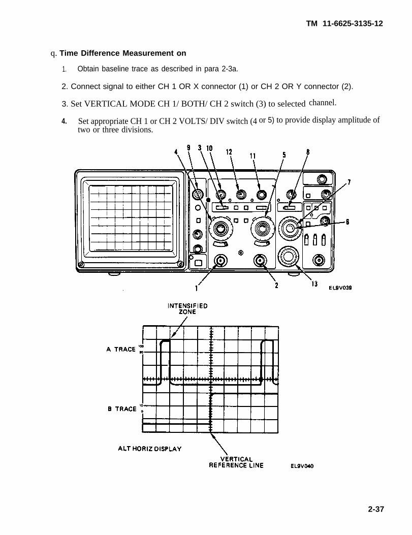
q. Time Difference Measurement on
1. Obtain baseline trace as described in para 2-3a.
2. Connect signal to either CH 1 OR X connector (1) or CH 2 OR Y connector (2).
3. Set VERTICAL MODE CH 1/ BOTH/ CH 2 switch (3) to selected channel.
4. Set appropriate CH 1 or CH 2 VOLTS/ DIV switch (4two or three divisions.
or 5) to provide display amplitude of
2-37

TM 11-6625-3135-12
5.
6.
7.
8.
9.
10.
11.
12.
Ensure that SEC/DIV variable control (6) is in CAL detent position and set A SEC/DIVSwitch (7) to sweep speed setting that displays measurement points on waveform.
Set HORIZONTAL MODE switch (8) to ALT.
Adjust B INTENSITY control (9) to display trace.
Adjust appropriate channel 1 or 2 vertical POSITION control (10 or 11) and A/B SWPSEP control ( 12) to display A trace above B trace.
Set B SEC/DIV control (7) to fastest sweep speed that provides visibleintensified zone.
Adjust B DELAY TIME POSITION control (13) to move intensified zone to leading edgeof first point of interest on A trace; then fine adjust until selected portion on B trace iscentered on any vertical graticule line. Record B DELAY POSITION control reading.
Adjust B DELAY TIME POSITION control clockwise to move intensified zone to leadingedge of second point of interest on A trace, then fine adjust until rising portion on B trace iscentered at same vertical graticule used in step (10). Record B DELAY TIME POSITIONcontrol (13) dial reading.
Calculate time difference between repetitive pules using formula
time seconddifference = dial -(duration) setting
first A SEC/DIVdial x switch
setting setting
EXAMPLE: A SEC/DIV switch is set to 0.2 ms per division, first B DELAY TIMEPOSITION control is set to 1.20, and second B DELAY TIME POSITION control is setto 9.53. Substituting given values:
Time difference = (9.53 - 1.20)(0.2 ms/div) = 1.666 ms
2-38 Change 1

TM 11-6625-3135-12
r. Measurement of Time Difference Between Pulses on Time-Related Signals.
1. Obtain baseline trace as described in para 2-3a.
2. Depress CH 1 TRIGGER SOURCE switch (1).
3. Set both AC/ GND/ DC switches (2 and 3) to desired position and ensure that both are setto same position.
4. Using either probes or cables with equal time delays, connect known reference signal to CH1 OR X connector (4) and comparison signal to CH 2 OR Y connector (5).
5. Set both CH 1 and CH 2 VOLTS/ DIV switches (6 and 7) for four- or five-division display.
6. Set VERTICAL MODE CH 1/BOTH/CH 2 switch (8) to BOTH.
7. Set VERTICAL MODE ADD/ALT/ CHOP switch (9) to either ALT or CHOP,depending on frequency of input signals.
8. If two signals are opposite polarities, pull out channel 2 vertical POSITION control (10) toinvert channel 2 display.
2-39

TM 11-6625-3135-12
9.
10.
11.
12.
Adjust A TRIGGER LEVEL control (11) for stable display.
Set A SEC/DIV switch (12) to sweep speed setting which provides three or more divisions of horizontal separation between reference points on two displays.
Rotate both vertical POSITION controls (10 and 13) to vertically center both displays.
Determine horizontal distance between two signal reference points and calculate timedifference using formula:
A SEC/DIV horizontalswitch setting x difference (divisions)
time difference =magnification factor
EXAMPLE: The A SEC/DIV switch is set to 50 us per division, the X10 magnifier is on(button out), and horizontal difference between signal measurement points is 4.5 divisions.Substituting the given values:
50 us/div x 4.5 div = 22.5 ustime difference =
10
2-40

TM 11-6625-3135-12
S. Time Difference Measurement Between Two Pulses on Two Time-Related Signals inDelayed Sweep Mode.
1. Obtain baseline trace as described in para 2-3a.
2. Depress CH 1 TRIGGER SOURCE switch (l).
3. Set VERTICAL MODE CH 1/BOTH/ CH 2 switch (2) to BOTH.
4. Set VERTICAL MODE ADD/ ALT/ CHOP switch (3) to ALT.
5. Using either probes or cables with equal time delays, connect known reference signal to CH1 OR X connector (4) and comparison signal to CH 2 OR Y connector (5).
6. Set both CH 1 and CH 2 VOLTS/DIV switches (6 and 7) for two- or three-division display.
7. Set
8. Set
9. Set
A SEC/DIV switch (8) to display measurement points within graticule area.
HORIZONTAL MODE switch (9) to ALT.
VERTICAL MODE CH 1/BOTH/CH 2 switch (2) to CH 1.
2-41
TM 11-66Z5-3135-12
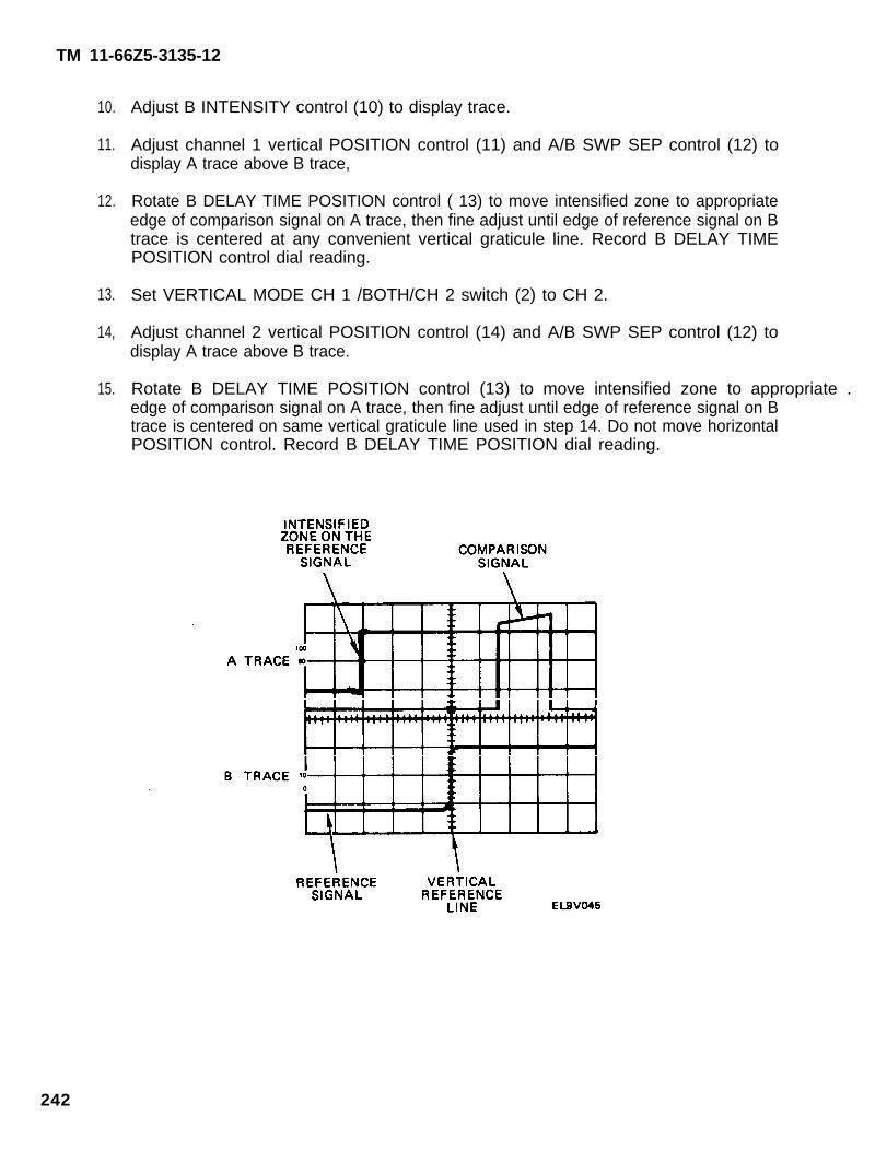
10.
11.
12.
13.
14,
15.
Adjust B INTENSITY control (10) to display trace.
Adjust channel 1 vertical POSITION control (11) and A/B SWP SEP control (12) todisplay A trace above B trace,
Rotate B DELAY TIME POSITION control ( 13) to move intensified zone to appropriateedge of comparison signal on A trace, then fine adjust until edge of reference signal on Btrace is centered at any convenient vertical graticule line. Record B DELAY TIMEPOSITION control dial reading.
Set VERTICAL MODE CH 1 /BOTH/CH 2 switch (2) to CH 2.
Adjust channel 2 vertical POSITION control (14) and A/B SWP SEP control (12) todisplay A trace above B trace.
Rotate B DELAY TIME POSITION control (13) to move intensified zone to appropriate .edge of comparison signal on A trace, then fine adjust until edge of reference signal on Btrace is centered on same vertical graticule line used in step 14. Do not move horizontalPOSITION control. Record B DELAY TIME POSITION dial reading.
242

TM 11-6625-3135-12
16. Calculate time difference between reference signal and comparison
time second first A SEC/DIVdifference = dial - dial x switch(duration) setting setting setting
signal using formula:
EXAMPLE: A SEC/DIV switch is set to 50 us per division, first B DELAY TIMEPOSITION control is set to 2.60, and second B DELAY TIME POSITION control is setto 7.10. Substituting given values:
time difference = (7.10 - 2.60)(50 us/div) = 225 us
2-43

TM 11-6625-3135-12
Section IV. OPERATION UNDER UNUSUAL CONDITIONS
2-4. OPERATION IN UNUSUAL WEATHER
The oscilloscope was designed as a bench-type instrument to be used in a controlled environment. Itdoes not have a weatherproof or waterproof case. It may be used outdoors as long as it is protectedfrom extreme heat, excessive cold, water, sand, mud, or similar conditions. Refer to chapter 1, para1-13, for oscilloscope specifications that should not be exceeded.
2-44

TM 11-6625-3135-12
CHAPTER 3ORGANIZATIONAL MAINTENANCE
Para Page
A and B Intensity Knobs Replacement. . . . . . . . . . . . . . . . . . . . . . . . . . . . . . . . . . . . .A and B SEC/DIV Knob Replacement . . . . . . . . . . . . . . . . . . . . . . . . . . . . . . . . . . . . CH 1 VOLTS/DIV and CH 2 VOLTS/DIV Knob Replacement . . . . . . . . . . Checking Unpacked Equipment . . . . . . . . . . . . . . . . . . . . . . . . . . . . . . . . . . . . . . Cleaning . . . . . . . . . . . . . . . . . . . . . . . . . . . . . . . . . . . . . . . . . . . . . . . . . . . .Common Tools and Equipment. . . . . . . . . . . . . . . . . . . . . . . . . . . . . . . . . . . . . . . . . . . .Initial Checks, Adjustments and Tests . . . . . . . . . . . . . . . . . . . . . . . . . . . . . . Line Fuse Replacement. . . . . . . . . . . . . . . . . . . . . . . . . . . . . . . . . . . . . . . . . . . .Operational Test. . . . . . . . . . . . . . . . . . . . . . . . . . . . . . . . . . . . . . . . . . . . . . . . . . . . . . . .Preparation for Storage or Shipment. . . . . . . . . . . . . . . . . . . . . . . . . . . . . . . . . . .Repair Parts. . . . . . . . . . . . . . . . . . . . . . . . . . . . . . . . . . . . . . . . . . . . . . . . . . . . . . . . . . .Safety Precautions. . . . . . . . . . . . . . . . . . . . . . . . . . . . . . . . . . . . . . . . . . . . . .Special Tools, TMDE, and Support Equipment . . . . . . . . . . . . . . . . .Troubleshooting Procedures. . . . . . . . . . . . . . . . . . . . . . . . . . . . . . . . . . . . . . . . . . . . . . .Types of Storage. . . . . . . . . . . . . . . . . . . . . . . . . .. . . . . . . . . . . . . . . . . . . . . . . . . . . .Unpacking . . . . . . . . . . . . . . . . . . . . . . . . . . . . . . . . . . . . . . . . . . . . . . . . . . . . .
3-113-133-123-53-143-13-63-103-93-153-33-73-23-83-163-4
3-83-103-93-23-113-13-23-73-53-123-13-33-13-33-123-2
Section I. REPAIR PARTS, SPECIAL TOOLS; TEST, MEASUREMENT,AND DIAGNOSTIC EQUIPMENT (TMDE); AND SUPPORT EQUIPMENT
3-1. COMMON TOOLS AND EQUIPMENT
Common tools and equipment required for organizational maintenance of Oscilloscope AN/USM-488 are listed in Appendix B (Maintenance Allocation Chart).
3-2. SPECIAL TOOLS, TMDE, AND SUPPORT EQUIPMENT
No special tools, TMDE, or support equipment are required.
3-3. REPAIR PARTS
Repair parts are listed and illustrated in the Repair Parts and Special Tools List (TM 11-6625-3135-24P).
3-1

TM 11-6625-3135-12
Section II. SERVICE UPON RECEIPT
3-4. UNPACKING
The oscilloscope is shipped assembled in its original packing container. Unpack carefully and do notdamage the container while unpacking. Save the container for use in reshipment.
3-5. CHECKING UNPACKED EQUIPMENT
a. Inspect the equipment for damage incurred during shipment. If the equipment has beendamaged, report the damage on Form SF 364, Report of Discrepancy.
b. Check the equipment against the packing slip to see if the shipment is complete. Report alldiscrepancies in accordance with the instructions of DA PAM 738-750.
c. Check to see whether the equipment has been modified.
3-6. INITIAL CHECKS, ADJUSTMENTS AND TESTS
a. Checks. Check that installed fuse in 1.0 amp, 250 volt, slow-blow.
b. Adjustments. Compensate probes as described in para 2-3b.
c. Tests. Perform complete operational test detailed in para 3-9.
3-2

TM 11-6625-3135-12
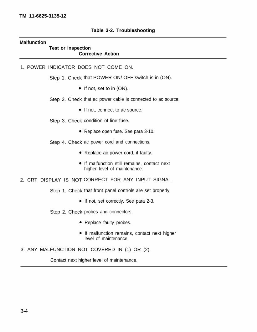
Section Ill. TROUBLESHOOTING
3-7. SAFETY PRECAUTIONS
WARNINGHigh voltage is used in the operation of this equipment. Death oncontact may result if you fail to observe safety precautions.
3-8. TROUBLESHOOTING PROCEDURES
The troubleshooting procedures listed in table 3-1 are those that may be done by organizationalmaintenance level personnel. Problems that may arise during operation are listed under malfunction.Tests or inspections to conduct and corrective actions to take to repair the malfunction are listed inthe two columns to the right of the malfunction column.
3-3
TM 11-6625-3135-12
Table 3-2. Troubleshooting
MalfunctionTest or inspection
Corrective Action
1. POWER INDICATOR DOES NOT COME ON.
Step 1. Check
Step 2. Check
Step 3. Check
Step 4. Check
2. CRT DISPLAY IS NOT
Step 1. Check
Step 2. Check
that POWER ON/ OFF switch is in (ON).
If not, set to in (ON).
that ac power cable is connected to ac source.
If not, connect to ac source.
condition of line fuse.
Replace open fuse. See para 3-10.
ac power cord and connections.
Replace ac power cord, if faulty.
If malfunction still remains, contact nexthigher level of maintenance.
CORRECT FOR ANY INPUT SIGNAL.
that front panel controls are set properly.
If not, set correctly. See para 2-3.
probes and connectors.
Replace faulty probes.
If malfunction remains, contact next higherlevel of maintenance.
3. ANY MALFUNCTION NOT COVERED IN (1) OR (2).
Contact next higher level of maintenance.
3-4

TM 11-6625-3135-12
Section IV. MAINTENANCE PROCEDURES
3-9. OPERATIONAL TEST
DESCRIPTION
This procedure covers: Operational readiness check of oscilloscope.
1.
2.
3.
4.
WARNINGDo not attempt to measure input signals that exceed the maximuminput signals listed in para 1-13.
Set POWER ON/ Off switch (1) to OFF (out).
Connect oscilloscope power cord to proper ac power source
Depress POWER ON/OFF switch (1).
POWER indicator comes on.
Obtain baseline trace as described in
Straight-line trace appears on
para 2-3a.
crt screen,
3-5

TM 1
5.
6.
7.
8.
9.
10.
11.
12.
13.
14.
15.
16.
1-6625-3135-12
Adjust A INTENSITY control (2) for desired display brightness.
Using channel 1 vertical POSITION control (3) and horizontal POSITION control (4), center trace on crt.
NOTE
If the trace is not parallel with the center horizontal graticule, adjustTRACE ROTATION pot (5).
Connect 10X probe to CH 1 OR X connector (5).
Set CH 1 VOLTS/DIV switch (6) to 0.1 10X PROBE.
Set channel 1 AC/ GND/ DC switch (7) to DC.
Set VERTICAL MODE CH 1/BOTH/CH 2 switch (8) to CH 1 and connect tip of 10X probe toAMP CAL connector (9).
. Trace on crt is square wave approximately five divisions in amplitude and 1 kHz infrequency.
Disconnect 10X probe from CH 1 OR X connector (5) and connect to CH 2 OR Y connector ( 10).
Set CH 2 VOLTS/DIV switch (11) to 0.1 10X PROBE.
Set CH 2 AC/GND/DC switch (12) to DC.
Set VERTICAL MODE CH 1/BOTH/CH 2 switch (8) to CH 2 and connect tip of 10 X probe toAMP CAL connector (9).
Trace on crt is square wave approximately five divisions in amplitude and 1 kHz infrequency.
Pull channel 2 vertical POSITION INVERT switch (13).
Crt display inverts.
Disconnect 10X probe and shut off oscilloscope, if desired.
END OF TASK
3-6

TM 11-6625-3135-12
3-10. LINE FUSE REPLACEMENT
DESCRIPTION
This procedure covers: Remove and Install.
REMOVE
1.
2.
3.
4.
5.
Ensure that POWER ON/ OFF switch (1)is set to OFF (out).
Disconnect ac power cord (2) from acsource.
Using common screwdriver, press in andslightly rotate fuseholder cap (3) in counter-clockwise direction to release fuseholdercap.
Withdraw fuseholder cap (3) with fuse (4)from fuseholder.
Remove fuse (4) from fuseholder cap (3).
INSTALL
1. Install new 1.0 A, 250 V, slow-blow fuse(4) into fuseholder cap (3).
2. Insert fuse F1 and fuseholder cap (3) intofuseholder.
3. Press in and slightly rotate fuseholder cap(3) in clockwise direction to secure fuse- holder cap.
4. Connect ac power cord (2) to ac source.
END OF TASK
3-7
TM 11-6625-3135-12
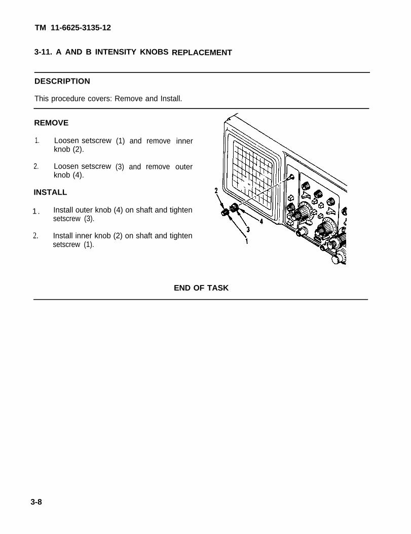
3-11. A AND B INTENSITY KNOBS REPLACEMENT
DESCRIPTION
This procedure covers: Remove and Install.
REMOVE
1. Loosen setscrewknob (2).
2. Loosen setscrewknob (4).
INSTALL
(1)
(3)
and
and
remove
remove
inner
outer
1 .
2.
Install outer knob (4) on shaft and tightensetscrew (3).
Install inner knob (2) on shaft and tightensetscrew (1).
END OF TASK
3-8

TM 11-6625-3135-12
3-12. CH 1 VOLTS/DIV AND CH 2 VOLTS/DIV KNOB REPLACEMENT
DESCRIPTION
This procedure covers: Remove and Install .
REMOVE
1. Loosen setscrew (1) and remove red calknob (2).
2. Remove outer knob (3)
INSTALL
1. Install outer knob (3) on plastic shaft.
2. Install red cal knob (2) and tightensetscrew (1).
END OF TASK
3-9

TM 11-6625-3135-12
3-13. A AND B SEC/DIV KNOB REPLACEMENT
DESCRIPTION
This procedure covers: Remove and Install.
REMOVE
1. Rotate control fully counterclockwise,then loosen setscrew (1) and remove redcal knob (2).
2. Loosen two setscrews (3) and remove grayknob (4).
3. Loosen two setscrewsclear plastic knob (6).
INSTALL
(5) and remove
1. Install clear plastic knob (6) and tightentwo setscrews (5).
2. Install gray knob (4) and tighten twosetscrews (3).
3. Install red knob (2) and tighten setscrew(1).
END OF TASK
3-10

TM 11-6825-313S-12
3-14. CLEANING
Loose dirt on the outside of the oscilloscope may be removed with a soft cloth or small soft-bristlebrush. Dirt that remains can be removed with a soft cloth dampened in a mild detergent and watersolution. Clean the light filter face with soft lint-free cloth dampened with either isopropyl alcohol,denatured ethyl alcohol, or mild detergent and water solution. The crt filter mesh should be cleanedonly with isopropyl or ethyl alcohol.
3-11

TM 11-6625-3135-12
Section V. PREPARATION FOR STORAGE OR SHIPMENT
3-15. PREPARATION FOR STORAGE OR SHIPMENT
If original packing material was saved, pack the oscilloscope in the same manner as it was received.When using packing materials other than the original, use the following guidelines:
a. Wrap oscilloscope in polyethylene sheeting before placing in container.
b. Select corrugated cardboard container having inside dimensions at least 6 inches greater thanoscilloscope dimensions and having a carton test strength of at least 275 pounds.
c. Use plenty of shock-absorbing material all around the oscilloscope to protect it againstdamage.
d. Seal the carton with shipping tape or an industrial stapler.
e. Mark container “FRAGILE-DELICATE INSTRUMENT” to insure proper handling.
3-16. TYPES OF STORAGE
a. Short-term (administrative) = 1 to 45 days. All equipment in this type must be made readywithin 24 hours for use on a mission. Make sure the next scheduled PMCS is done and all deficienciescorrected before placing in storage. The storage site should provide protection from extreme weatherconditions and allow you to reach it for inspections or exercises, if needed.
b. Intermediate = 46 to 180 days.
c. Long-term = over 180 days.
3-12

TM 11-6625-3135-12
APPENDIX AREFERENCES
A-1. SCOPEThis appendix lists all forms, field manuals, technical manuals, and miscellaneous publications referenced in this manual.
A-2. FORMSRecommended Changes to Publications and Blank Forms . . . . . . . . . . . . . . . . . . . . . . . . . . . . . . . .
Recommended Changes to Equipment Technical Manuals . . . . . . . . . . . . . . . . . . . . . . . . . . . . . . . .
Equipment Inspection and Maintenance Worksheet . . . . . . . . . . . . . . . . . . . . . . . . . . . . . . . . . . . . .Report of Discrepancy . . . . . . . . . . . . . . . . . . . . . . . . . . . . . . . . . . . . . . . . . . . . . . . . . . . . . . . . . . . .
Product QualityDeficiencyReport. . . . . . . . . . . . . . . . . . . . . . . . . . . . . . . . . . . . . . . . . . . . . . . . . .
A-3. TECHNICAL MANUALSThe Army Maintenance Management Systems (TAMMS) . . . . . . . . . . . . . . . . . . . . . . . . . . . . . . . .
Procedures for Destruction of Electronics Materiel to PreventEnemy Use (Electronics Command) . . . . . . . . . . . . . . . . . . . . . . . . . . . . . . . . . . . . . . . . . . . . . . . . .
Organizational, Direct Support and General Support Repair Parts andSpecial Tools List,Oscilloscope AN/USM-488 (NSN 6625-01–187-7847) . . . . . . . . . . . . . . . . . .
A-4. MISCELLANEOUS
Common Table of Allowances . . . . . . . . . . . . . . . . . . . . . . . . . . . . . . . . . . . . . . . . . . . . . . . . . . . . . .
Consolidated Index of Army Publications and Blank Forms . . . . . . . . . . . . . . . . . . . . . . . . . . . . . . .
Safety Precautions for Maintenance of Electrical/ElectronicEquipment . . . . . . . . . . . . . . . . . . . . .
First Aid for Soldiers . . . . . . . . . . . . . . . . . . . . . . . . . . . . . . . . . . . . . . . . . . . . . . . . . . . . . . . . . . . . .
Abbreviations for Use on Drawings, Specifications, Standardsand in Technical Documents . . . . . . . . . . . . . . . . . . . . . . . . . . . . . . . . . . . . . . . . . . . . . . . . . . . . . . .
DA Form 2028
DA Form 2028-2
DA Form 2404
Form SF 364
Form SF 368
DA Pam 738-750
TM 750-2442
TM11-6625-3135-24P
CTA 50-970
DA Pam 25-30
TB 385-4
FM 21-11
MIL-STD-12
Change 1 A-1/(A-2blank)

TM 11-6625-3135-12
APPENDIX BMAINTENANCE ALLOCATION CHART
Sectlon l. INTRODUCTION
B-1. General
a. This section provides a general explanation of allmaintenance and repair functions authorized at variousmaintenance categories.
b. The Maintenance Allocation Chart (MAC) in sec-tion II designates overall authority and responsibility forthe performance of maintenance functions on the identi-fied end item or component. The application of the main-tenance functions to the end item or component will beconsistent with the capacities and capabilities of the desig-nated maintenance categories,
c. Section III lists the tools and test equipment (bothspecial tools and common tool sets) required for eachmaintenance function as referenced from section II.
d. Section IV contains supplemental instructions andexplanatory notes for a particular maintenance function.
B-2. Maintenance Functions
Maintenance functions will be limited to and defined asfollows:
a. Inspect. To determine the serviceability of an item bycomparing its physical, mechanical, and /or electrical char-acteristics with established standards through examination(e.g., by sight, sound, or feel).
b, Test. To verify serviceability by measuring the mechan-ical and electrical characteristics of the oscilloscope andcomparing these characteristics with prescribed standards.
c. Service, Operations required periodically to keep theoscilloscope in proper operating condition; i.e., to clean (ordecontaminate), to preserve, etc.
d. Adjust. To maintain, within prescribed limits, bybringing into proper or exact position, or by setting theoperating characteristics to specified parameters,
e. Replace. To remove an unserviceable item and installa serviceable counterpart in its place. Replace is authorizedby the MAC and is shown as the third position code of theSMR code.
f. Repair. The application of maintenance services,including fault location/ troubleshooting, removal/ instal-lation, and disassembly/ assembly procedures, and main-tenance actions to identify troubles and restore serviceabil-ity to an item by correcting specific damage, fault, malfunc-tion, or failure in a part, subassembly, module, or end itemor system.
B-3. Explanation of Columnsin the MAC (Section II)
a. Column 1, Group Number. Column 1 lists functionalgroup code numbers, the purpose of which is to identifymaintenance significant components, assemblies, subas-semblies, and modules with the next higher assembly. Enditem group number shall be 00.
b. Column 2, Component/Assembly. Column 2 con-tains the names of components, assemblies, subassemblies,and modules for which maintenance is authorized.
c. Column 3, Maintenance Function. Column 3 liststhe functions to be performed on the item listed in column 2(see para B-2).
d. Column 4, Maintenance Category. Column 4 speci-fies, by the listing of a “worktime’’ figure in the appropriatesubcolumn(s), the category of maintenance authorized toperform the function listed in column 3. This figure repres-ents the active time required to perform that maintenancefunction at the indicated category of maintenance. If thenumber or complexity of the tasks within the listed main-tenance function vary at different maintenance categories,appropriate “worktime” figures will be shown for eachcategory. The “worktime” figure represents the averagetime required to restore an item (assembly, subassem-bly, component, module, end item, or system) to a service-able condition under typical field operating conditions.This time includes preparation time (including any neces-sary disassembly/ assembly time), troubleshooting/faultlocation time, and quality assurance/ quality control time
B-1

TM 11-6625-3135-12
in addition to the time required to perform the specifictasks identified for the maintenance functions authorizedin the MAC. The symbol designations for the maintenancecategories are as follows:
c — Operator or CrewO — Organizational MaintenanceF — Direct Support MaintenanceH — General Support MaintenanceD — Depot Maintenance
e. Column 5, Tools and Equipment. Column 5 specifiesby code, those common tool sets (not individual tools) andspecial tools, TM DE, and support equipment required toperform the designated function.
f. Column 6, Remarks. This column shall, when appli-cable, contain a letter code, in alphabetic order, which shallbe keyed to the remarks contained in section IV.
B-4. Explanation of Columns inTool and Test Equipment Requirement(Section Ill)
a. Column 1, Reference Code. The tool and test equip-ment reference code correlates with a code used in theMAC, section II, column 5.
b. Column 2, Maintenance Category. The lowest cate-gory of maintenance authorized to use the tool or testequipment.
c. Column 3, Nomenclature. Name or identification ofthe tool or test equipment
d. Column 4, National Stock Number, The nationalstock number of the tool or test equipment.
e. Column 5, Tool Number. The manufacturer’s partnumber.
B-5. Explanation of Columns in Remarks(Section IV)
a. Column 1, Reference Code. The code recorded incolumn 6, section II.
b. Column 2, Remarks, This column lists informationpertinent to the maintenance function being performed asindicated in the MAC, section II.
B-2

TM11-6625-3135-12
SECTION II. MAINTENANCE ALLOCATION CHARTFOR
OSCILLOSCOPE AN/USM-488
B-3

TM 11-6625-313S-12
SECTION Ill. TOOL AND TEST EQUIPMENT REQUIREMENTSFOR
OSCILLOSCOPE AN/USM-488
B-4

TM11-6625-313S-12
SECTION IV. REMARKS
B-5(B-6 blank)


TM 11-6625-3135-12
APPENDIX CCOMPONENTS OF END ITEM AND BASIC ISSUE ITEMS LISTS
Section i. INTRODUCTION
C-1. SCOPE
This appendix lists components of end item and basic issue items for the Oscilloscope AN/ USM-488to help you inventory items required for safe and efficient operation.
C-2. GENERAL
The Components of End Item and Basic Issue Items Lists are divided into the following sections:
a. Section Il. Components of End Item. This listing is for informational purposes only, and isnot authority to requisition replacements. These items are part of the end item, but are removed andseparately packaged for transportation or shipment. As part of the end item, these items must be withthe end item whenever it is issued or transferred between property accounts. Illustrations arefurnished to assist you in identifying the items.
b. Section Ill. Basic Issue Items (Bll). These are the minimum essential items required to placethe oscilloscope in operation, to operate it, and to perform emergency repairs. Although shippedseparately packaged, BII must be with the oscilloscope during operation and whenever it is trans-ferred between property accounts. The illustrations will assist you with hard-to-identify items. Thismanual is your authority to request/requisition replacement BII, based on TOE/MTOE authoriza-tion of the end item.
C-3. EXPLANATION OF COLUMNS
The following is an explanation of columns found in the tabular listings:
a. Column (1) - Illustration Number (Illust. No.). This column indicates the number of theillustration in which the item is shown.
b. ‘Column (2) - National Stock Number. Indicates the National stock number assigned to theitem and will be used for requisitioning purposes.
c. Column (3) - Description. Indicates the Federal item name and, if required, a minimumdescription to identify and locate the item. The last line for each item indicates the Federal SupplyCode for Manufacturer (FSCM) (in parentheses) followed by the part number. If item needed differsfor different models of this equipment, the model is shown under the Usable On heading in this column.
d. Column (4) - Unit of Measure (U/M). Indicates the measure used in performing the actualoperational/ maintenance function. This measure is expressed by a two-character alphabeticalabbreviation (e.g., ea, in, pr).
e. Column (5) - Quantity Required (Qty Rqr). Indicates the quantity of the item authorized tobe used with the oscilloscope.
C-1
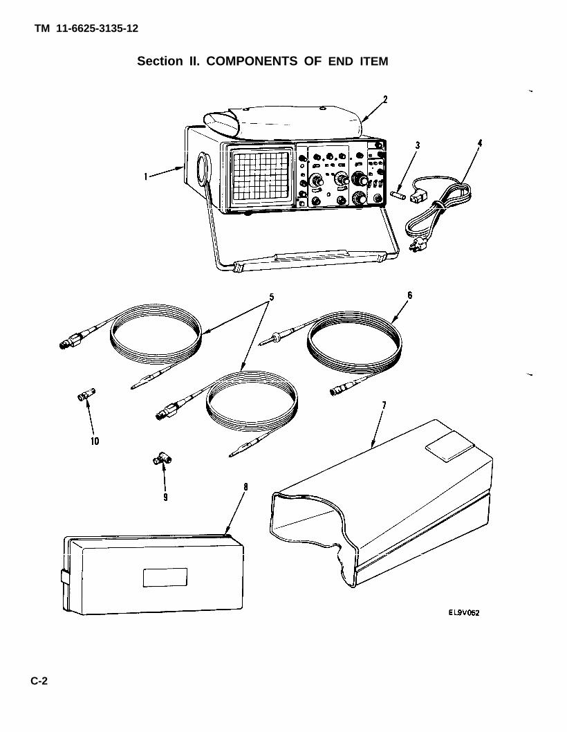
TM 11-6625-3135-12
Section II. COMPONENTS OF END ITEM
C-2
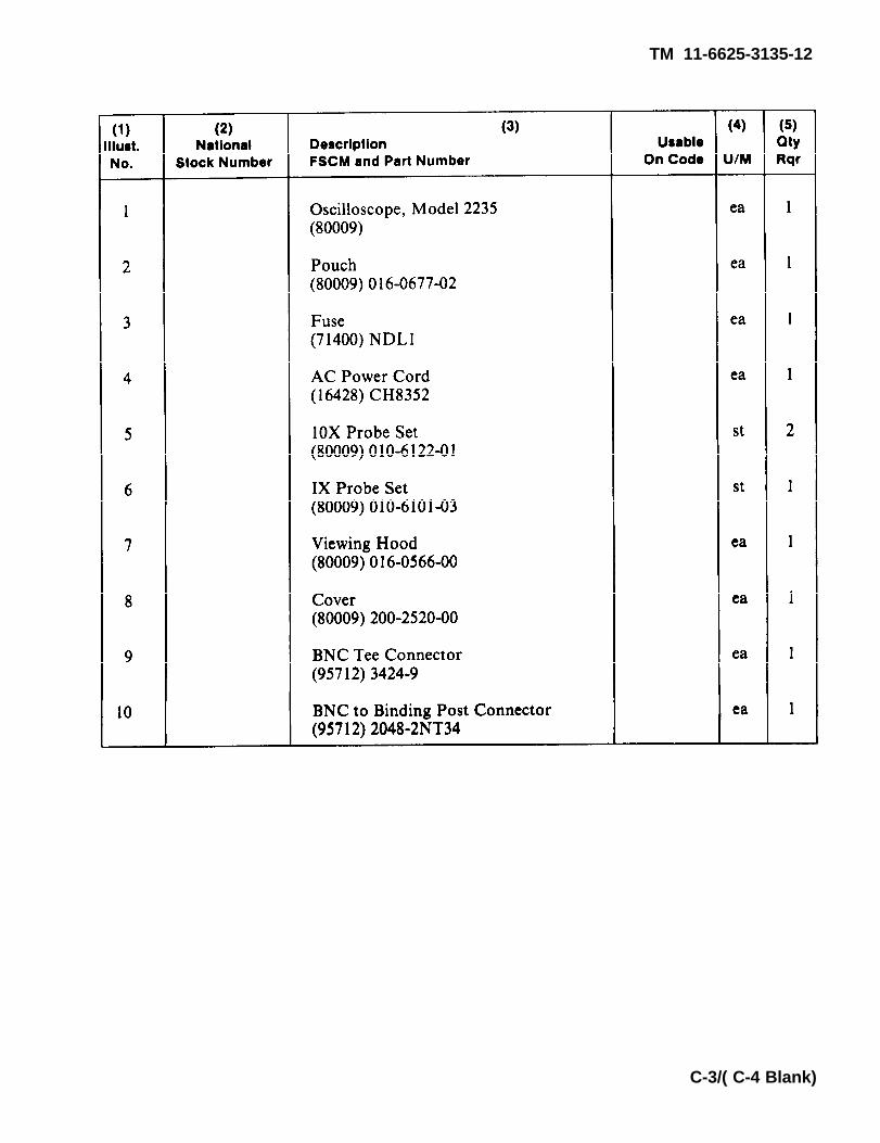
TM 11-6625-3135-12
C-3/( C-4 Blank)

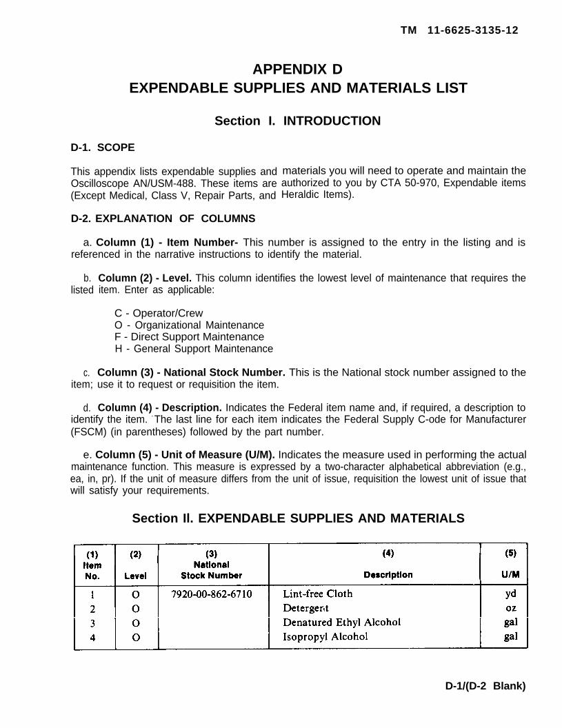
TM 11-6625-3135-12
APPENDIX DEXPENDABLE SUPPLIES AND MATERIALS LIST
Section I. INTRODUCTION
D-1. SCOPE
This appendix lists expendable supplies andOscilloscope AN/USM-488. These items are(Except Medical, Class V, Repair Parts, and
D-2. EXPLANATION OF COLUMNS
materials you will need to operate and maintain theauthorized to you by CTA 50-970, Expendable itemsHeraldic Items).
a. Column (1) - Item Number- This number is assigned to the entry in the listing and isreferenced in the narrative instructions to identify the material.
b.listed
c.item;
d.
Column (2) - Level. This column identifies the lowest level of maintenance that requires theitem. Enter as applicable:
C - Operator/CrewO - Organizational MaintenanceF - Direct Support MaintenanceH - General Support Maintenance
Column (3) - National Stock Number. This is the National stock number assigned to theuse it to request or requisition the item.
Column (4) - Description. Indicates the Federal item name and, if required, a description toidentify the item. - The last line for each item indicates the Federal Supply C-ode for Manufacturer(FSCM) (in parentheses) followed by the part number.
e. Column (5) - Unit of Measure (U/M). Indicates the measure used in performing the actualmaintenance function. This measure is expressed by a two-character alphabetical abbreviation (e.g.,ea, in, pr). If the unit of measure differs from the unit of issue, requisition the lowest unit of issue thatwill satisfy your requirements.
Section Il. EXPENDABLE SUPPLIES AND MATERIALS
D-1/(D-2 Blank)


TM 11-6625-3135-12
I N D E X
Subject
A
A and B Intensity Knobs Replacement . . . . . . . . . . . . . . . . . . . . . . . . . . . . . . . . . . . . . . . . . . .A and B Sec/Div Knob Replacement . . . . . . . . . . . . . . . . . . . . . . . . . . . . . . . . . . . . . . . . . . . .Abbreviations. List of . . . . . . . . . . . . . . . . . . . . . . . . . . . . . . . . . . . . . . . . . . . . . . . . . . . . . . . . . . . .Algebraic Addition, Operating Procedures . . . . . . . . . . . . . . . . . . . . . ..... . . . . . . . . . . . .
Amplitude Comparison (Ratio), Operating Procedures . . . . . . . . . . . . . . . . . . . . . . . . . .AN/USM-488 Oscilloscope Block Diagram . . . . . . . . . . . . . . . . . . . . . . . . . . . . . . . . . . . . . .Appendices
A — References . . . . . . . . . . . . . . .. .. . . . . . . . . . . . . . . . . . . . . . . . . . . . . . . . . . . . . . . . . . . . . . . . . . . . . . .B— Maintenance Allocation Chart . . . . . . . . . . . . . . . . . . . . . ...... . . . . . . . . . . . . . . .C — Components of End Item and Basic Issue Items Lists . . . . . . . . . . . . . . . . . . . .D — Expendable Supplies and Materials List . . . . . . . . . . . ..... . . . . . . . . . . . .
C
CH 1 Volts/Div and CH2 Volts/Div Knob Replacement . . . . . . . . . . . . . . . . . . . . . . .Checking Unpacked Equipment . . . . . . . . . . . . . . . . . . . . . . . . . . . . . . . . . . . . . . . . . . . . . . . . . .Cleaning . . . . .. . . . . . . . . . . . . . . . . . . . . . . . . .. . . . . . . . . . . . . . . . . . . . . . . . . . . . . . . . . . . .. . . . . . . . . . . . .Common Tools and Equipment . . . . . . . . . . . . . . . ... . .. . . . .. . . . . . .. . . . . . . . . . . . .. . . . . . . . . . . .. . .Common-Mode Rejection, Operating Procedures . . . . . .. ... .... . . . .... . . . . . . . .Components of End Item and Basic Issue Items Lists . . . .... . . . . . . . . .. . . .Consolidated Index of Army Publications and Blank Forms . . . . . . . . . . . . . . . . . . . . .Controls, Preset Positions . . . . . . . . . . . . . . . . . . . . . . . . . . . . . . . . . . . ..... . . . . . . . . . . . . . . .
D
Destruction of Army Material to Prevent Enemy Use . . . . . . . . .
E
Equipment DescriptionEquipment Characteristics, Capabilities, and Features . . . . . . . . . . . . . . . . . . . . . . . .Equipment Data . . . . . . . . . . . . . . . ...... . ...... . . . . . . . . . . . . . . . . . . . . . . . ... . . . . . .Location and Description of Major Components . ....... . . . . . . . . . . . . . . . . . . . . .
Expendable Supplies and Materials List . . . . . . . . . . . . . . . ...... . . . . . . . . . . .
F
Frequency Measurement, Operating Procedures . . . . . . . . . . . . . . . . . . . . . . . . . .. .Functional Description . . . . . . . . . . . . . . . . . . . . . . . . . . . . . . . . . . . . . . . ..... .
Paragraph,Figure, Table,
Number
3-113-131-102-3e2-3g
F 1-2
A-1B-1C-1D-1
3-123-53-143-12-3fC-11-2
T 2-2
1-4
1-111-131-12D-1
2-3i1-14— .
Index-1

TM 11-6625-3135-12
Subject
Paragraph,Figure, Table,
Number
G
General InformationConsolidated Index of Army Publications and Blank Forms . . . . . . . . . . . . . . . . . .Destruction of Army Material to Prevent Enemy Use . . . . . . . . . . . . . . . . . . . . . . . . .List of Abbreviations . . . . . . . . . . . . . . . . . . . . . . . . . . . . . . . . . . . . . . . . . . . . . . . . . . . . . . . . . .Maintenance Forms, Records, and Reports . . . . . . . . . . . . . . . . . . . . . . . . . . . . . . . . . . . .Nomenclature Cross-Reference List . . . . . . . . . . . . . . . . . . . . . . . . . . . . . . . . . . . . . . . . . . . .Preparation for Storage or Shipment . . . . . . . . . . . . . . . . . . . . . . . . . . . . . . . . . . . . . . . . . .Reporting Equipment Improvement Recommendations (EIR) . . . . . . . . . . . . . . . .Safety .Care. and Handling . . . . . . . . . . . . . . . . . . . . . . . . . . . . . . . . . . . . . . . . . . . . . . . . . . . .Scope . . . . . . . . . . . . . . . . . . . . . . . . . . . . . . . . . . . . . . . . . . . . . . . . . . . . . . . . . .. . . . . . . . .....Warranty Information . . . . . . . . . . . . . . . . . . . . . . . . . . . . . . . . . . . . . . . . . . . . . . . . . . . . . . . . .
I
Initial Checks, Adjustments and Tests.. . . . . . . . . . . . . . . . . . . . . . . . . . . . . . . . . . . . . . . . . . .Instantaneous Voltage Measurement, Operating Procedures . . . . . . . . . . . . . . . . . . . . .
L
Line Fuse Replacement . . . . . . . . . . . . . . . . . . . . . . . . . . . . . . . . . . . . . . . . . . . . . . . . . . . . . . . . . .List of Abbreviations . . . . . . . . . . . . . . . . . . . . . . . . . . . . . . . . . . . . . . . . . . . . . . . . . . . . . . . . . . . . .Location and Description of Major Components . . . . . . . . . . . . . . . . . . . . . . . . . . . . . . . .
M
Magnified Sweep Runs After Delay, Operating Procedures . . . . . . . . . . . . . . . . . . . . . .Maintenance Allocation Chart . . . . . . . . . . . . . . . . . . . . . . . . . . . . . . . . . . . . . . . . . . . . . . . . . . .Maintenance Forms, Records, and Reports . . . . . . . . . . . . . . . . . . . . . . . . . . . . . . . . . . . . . .Maintenance Procedures
A and B Intensity Knobs Replacement . . . . . . . . . . . . . . . . . . . . . . . . . . . . . . . . . . . . . . . .A and B Sec/DivKnobReplacement . . . . . . . . . . . . . . . . . . . . . . . . . . . . . . . . . . . . . . . . . .CH 1 Volts/ Div and CH 2 Volts/Div Knob Replacement . . . . . . . . . . . . . . . . . . . . .Cleaning . . . . . . . .. . . .. . . . . . ... . . . . . . . . . . . . . . . . . . . . . .. . . .. . . . . .. . . . . .Line Fuse Replacement . . . . . . . . . . . . . . . . . . . . . . . . . . . . . . . . . . . . . . . . . . . . . . . . . . . . . . . .Operational Test . . . . . . . . . . . . . . . . . . . . . . . . . . . . . . . . . . . . . . . . . . . . . . . . . . . . . . . . . . . . . . .
Measurement of Time Difference Between Pulses on Time-Related Signals,Operating Procedures . . . . . . . . . . . . . . . . . . . . . . . . . . . . . . . . . . . . . . . . . . . . . . . . . . . . . . . . . . . .
N
Nomenclature Cross-Reference List . . . . . . . . . . . . . . . . . . . . . . . . . . . . . . . . . . . . . . . . . . . . . .
1-21-41-101-31-71-51-81-81-11-9
3-62-3d
3-101-101-12
2-3mB-11-3
3-113-133-123-143-103-9
2-3r
1-7
Index-2

Subject
TM 11-6625-3135-12
O
Obtaining Baseline Trace, Operating Procedures . . . . . . . . . . . . . . . . . . . . . . . . . . . . . . . . .Operating Procedures . . . . . . . . . . . . . . . . . . . . . . . . . . . . . . . . . . . . . . . . . . . . . . . . . . . . . . . . . . . .Operation in Unusual Weather . . . . . . . . . . . . . . . . . . . . . . . . . . . . . . . . . . . . . . . . . . . . . . . . . . .Operation Under Usual Conditions
Operating Procedures . . . . . . . . . . . . . . . . . . . . . . . . . . . . . . . . . . . . . . . . . . . . . . . . . . . . . . . . . .Algebraic Addition . . . . . . . . . . . . . . . . . . . . . . . . . . . . . . . . . . . . . . . . . . . . . . . . . . . . . . . . . .Amplitude Comparison (Ratio) . . . . . . . . . . . . . . . . . . . . . . . . . . . . . . . . . . . . . . . . . . . . .Common-Mode Rejection . . . . . . . . . . . . . . . . . . . . . . . . . . . . . . . . . . . . . . . . . . . . . . . . . . .Frequency Measurement . . . . . . . . . . . . . . . . . . . . . . . . . . . . . . . . . . . . . . . . . . . . . . . . . . . .Instantaneous Voltage Measurement . . . . . . . . . . . . . . . . . . . . . . . . . . . . . . . . . . . . . . . .Magnified Sweep Runs After Delay . . . . . . . . . . . . . . . . . . . . . . . . . . . . . . . . . . . . . . . . .Measurement of Time Difference Between Pulses onTime-Related Signals . . . . . . . . . . . . . . . . . . . . . . . . . . . . . . . . . . . . . . . . . . . . . . . . . . . . . . . .Obtaining Baseline Trace . . . . . . . . . . . . . . . . . . . . . . . . . . . . . . . . . . . . . . . . . . . . . . . . . . . .Peak-To-Peak Voltage Measurements . . . . . . . . . . . . . . . . . . . . . . . . . . . . . . . . . . . . . . .Phase Difference Measurement . . . . . . . . . . . . . . . . . . . . . . . . . . . . . . . . . . . . . . . . . . . . . .Probe Compensation . . . . . . . . . . . . . . . . . . . . . . . . . . . . . . . . . . . . . . . . . . . . . . . . . . . . . . . .Pulse Jitter Time Measurement . . . . . . . . . . . . . . . . . . . . . . . . . . . . . . . . . . . . . . . . . . . . . .Rise Time Measurement in Delayed-Sweep Mode . . . . . . . . . . . . . . . . . . . . . . . . . . .Rise Time Measurement . . . . . . . . . . . . . . . . . . . . . . . . . . . . . . . . . . . . . . . . . . . . . . . . . . . . .Time Difference Measurement Between Two Pulses on TwoTime-Related Signals in Delayed Sweep Mode . . . . . . . . . . . . . . . . . . . . . . . . . . . . . .Time Difference Measurement on Single Waveform . . . . . . . . . . . . . . . . . . . . . . . .Time Duration Measurement. . . . . . . . . . . . . . . . . . . . . . . . . . . . . . . . . . . . . . . . . . . . . . . .Triggered Magnified Sweep Measurement . . . . . . . . . . . . . . . . . . . . . . . . . . . . . . . . . . .
Operational Test . . . . . . . . . . . . . . . . . . . . . . . . . . . . . . . . . . . . . . . . . . . . . . . . . . . . . . . . . . . . . . . . .Operator Preventive Maintenance Checks and Services (PMCS)
General . . . . . . . . . . . . . . . . . . . . . . . . . . . . . . . . . . . . . . . . . . . . . . . . ..PMCS Table . . . . . . . . . . . . . . . . . . . . . . . . . . . . . . . . . . . . . . . . . . .
Oscilloscope AN/USM-488 . . . . . . . . . . . . . . . . . . . . . . . . . . . . . . . . . . . . . . . . . . . . . . . . . . . . . .Oscilloscope PMCS Location Diagram . . . . . . . . . . . . . . . . . . . . . . . . . . . . . . . . . . . . . . . . .
P
Peak-To-Peak Voltage Measurements, Operating Procedures . . . . . . . . . . . . . . . . . . . .Phase Difference Measurement, Operating Procedures . . . . . . . . . . . . . . . . . . . . . . . . . .PMCS Table . . . . . . . . . . . . . . . . . . . . . . . . . . . . . . . . . . . . . . . . . . . . . . . . ...Preparation for Storage or Shipment
Preparation for Storage or Shipment . . . . . . . . . . . . . . . . . . . . . . . . . . . . . . . . . . . . . . . . . .Types of Storage . . . . . . . . . . . . . . . . . . . . . . . . . . . . . . . . . . . . . . . . . . . . . . . . . . . . . . . . . . . . . . .
Intermediate . . . . . . . . . . . . . . . . . . . . . . . . . . . . . . . . . . . . . . . . . . . . . . . . . . .Long-term . . . . . . . . . . . . . . . . . . . . . . . . . . . . . . . . . . . . . . . . . . . . . . . . . . . . Short-term (administrative) . . . . . . . . . . . . . . . . . . . . . . . . . . . . . . . . . . . . . . . . . . . . . . . . . .
Paragraph,Figure, Table,
Number
2-3a2-32-4
2-32-3e2-3g2-3f2-3i2-3d2-3m
2-3r2-3a2-3c2-312-3b2-3n2-3k2-3j
2-3s2-3q2-3h2-3p3-9
2-12-2
F 1-1F 2-1
2-3c2-312-2
3-153-163-16b3-16c3-16a
Index-3
TM 11-6625-3135-12
Subject
Preparation for Storage or Shipment . . . . . . . . . . . . . . . . . . . . . . . . . . . . . . . . . . . . . . . . . . . .Probe Compensation, Operating Procedures . . . . . . . . . . . . . . . . . . . . . . . . . . . . . . . . . . . . .Pulse Jitter Time Measurement, Operating Procedures . . . . . . . . . . . . . . . . . . . . . . . . . .
R
References . . . . . . . . . . . . . . . . . . . . . . . . . . . . . . . . . . . . . . . . . . . . . . . . . . . . . . . . . . . . . . . . . . . . . . . .Remarks . . . . . . . . . . . . . . . . . . . . . . . . . . . . . . . . . . . . . . . . . . . . . . . . . . . . . . . . . . . . . . . . . . . . . . . . . .Repair Parts, Special Tools; Test, Measurement, and DiagnosticEquipment (TMDE); and Support Equipment
Common Tools and Equipment . . . . . . . . . . . . . . . . . . . . . . . . . . . . . . . . . . . . . . . . . . . . . . . .Repair Parts . . . . . . . . . . . . . . . . . . . . . . . . . . . . . . . . . . . . . . . . . . . . . . . . . . . . . . . . . . . . . . . . . . .Special Tools, TMDE, and Support Equipment . . . . . . . . . . . . . . . . . . . . . . . . . . . . . . .
Reporting Equipment Improvement Recommendations (EAR) . . . . . . . . . . . . . . . . . . .Rise Time Measurement in Delayed-Sweep Mode, Operating Procedures . . . . . . .Rise Time Measurement, Operating Procedures . . . . . . . . . . . . . . . . . . . . . . . . . . . . . . . . . .
Safety Precautions . . . .Safety, Care, and Hand
S
. . . . . . . . . . . . . . . . . . . . . . . . . . . . . . . . . . . . . . . . . . . . . . . . . . . . . . . . . .ing . . . . . . . . . . . . . . . . . . . . . . . . . . . . . . . . . . . . . . . . . . . . . . . . . . . . . .
Scope . . . . . . . . . . . . . . . . . . . . . . . . . . . . . . . . . . . . . . . . . . . . . . . . . . . . . . . . . . . . . . . . . . . . . . . . . . . . .Service Upon Receipt
Checking Unpacking Equipment . . . . . . . . . . . . . . . . . . . . . . . . . . . . . . . . . . . . . . . . . . . . . . .Initial Checks, Adjustments and Tests . . . . . . . . . . . . . . . . . . . . . . . . . . . . . . . . . . . . . . . . .Unpacking . . . . . . . . . . . . . . . . . . . . . . . . . . . . . . . . . . . . . . . . . . . . . . . . . . . . . . . . . . . . . . . . . . . . .
Special Tools, TMDE, and Support Equipment . . . . . . . . . . . . . . . . . . . . . . . . . . . . . . . . .
T
Technical Principles of OperationFunctional Description . . . . . . . . . . . . . . . . . . . . . . . . . . . . . . . . . . . . . . . . . . . . . . . . . . . . . . . .
Time Difference Measurement Between Two Pulses on TwoTime-Related Signals in Delayed Sweep Mode, Operating Procedures . . . . . . . . . . .Time Difference Measurement on Single Waveform, Operating Procedures . . . . .Time Duration Measurement, Operating Procedures . . . . . . . . . . . . . . . . . . . . . . . . . . . .Tool and Test Equipment Requirements for Oscilloscope AN/USM-488... . . . . .Triggered Magnified Sweep Measurement, Operating Procedures . . . . . . . . . . . . . . .Troubleshooting
Safety Precautions . . . . . . . . . . . . . . . . . . . . . . . . . . . . . . . . . . . . . . . . . . . . . . . . . . . . . . . . . .Troubleshooting Procedures.. . . . . . . . . . . . . . . . . . . . . . . . . . . . . . . . . . . . . . . . . . . . . . . . . .
Types of Storage . . . . . . . . . . . . . . . . . . . . . . . . . . . . . . . . . . . . . . . . . . . . . . . . . . . . . . . . . . . . . . . . .
Paragraph,Figure, Table,
Number
1-5, 3-152-3b2-3n
A-1B-5
3-13-33-21-82-3k2-3j
3-71-61-1
3-53-63-43-2
1-14
2-3Ss2-3q2-3hB-42-3p
3-73-83-16
Index-4

TM11-6625-3135-12
Paragraph,Figure, Table,
NumberSubject
U
Unpacking . . . . . . . . ...... .. . . .. . . . .. . . . . . . . . . . . . . . . . . . . . . . . . . . . . . . . . . . . . . . . . . . . . . . . . . . . . . . .
W
3-4
Warranty Information . . . . . . . . . . . . . . . . . . . . . . . . . . . . . . . . . . . . . . . . . . . 1-8
Index-5/(lndex-6 Blank)

TM 11-6625-3135-40
TECHNICAL MANUAL
This copy is a reprint which includes current
G E N E R A L S U P P O R T
M A I N T E N A N C E M A N U A L
OSCILLOSCOPEAN/USM-488
(NSN 6625-01-187-7847)
EQUIPMENTDESCRIPTION
PAGE 1-4
SERVICE UPONRECEIPT
PAGE 2-2
MAINTENANCEPROCEDURES
PAGE 2-36
HEADQUARTERS, DEPARTMENT OF THE ARMY
15 OCTOBER 1986
pages from change 1.
S Y M P T O MINDEX
PAGE 2-3
S U B J E C TINDEX
PAGE INDEX-1

TM 11-6625-3135-40
SAFETY STEPS TO FOLLOW IF SOMEONE IS THE VICTIM OFELECTRICAL SHOCK
DO NOT TRY TO PULL OR GRAB THE INDIVIDUAL
IF POSSIBLE, TURN OFF THE ELECTRICAL POWER
IF YOU CANNOT TURN OFF THE ELECTRICAL POWER, PULL,PUSH, OR LIFT THE PERSON TO SAFETY USING A WOODEN POLEOR A ROPE OR SOME OTHER INSULATING MATERIAL
SEND FOR HELP AS SOON AS POSSIBLE
AFTER THE INJURED PERSON IS FREE OF CONTACT WITH THESOURCE OF ELECTRICAL SHOCK, MOVE THE PERSON A SHORTDISTANCE AWAY AND IMMEDIATELY START ARTIFICIALRESUSCITATION

TM 11-6625-3135-40
W A R N I N G
HIGH VOLTAGE
is used in the operation of this equipment
DEATH ON CONTACT
may result if personnel fail to observe safety precautions
Never work on electronic equipment unless there is is another person nearly who is familiar withthe operation and hazards of the equipment and who is competent in administering first aid. Whentechnicians are aided by operators, they must be warned about dangerous areas.
A periodic review of safety precautions in TB 385-4, Safety Precautions for Maintenance ofElectrical/Electronic Equipment, is recommended. When the equipment is operated with coversremoved, DO NOT TOUCH exposed connections or components, MAKE CERTAIN you are notgrounded when making connections or adjusting components inside the test instrument.
Be careful not to contact high-voltage connections or 115 volt ac input connections wheninstalling or operating this equipment.
Whenever the nature of the operation permits, keep one hand away from the equipment to reducethe hazard of current flowing through the body.
WARNING Do not be misled by the term “low voltage”, Potentials as low as50 volts may cause death under adverse conditions.
For Artificial Respiration, refer to FM 21-1 I
B

TM 11-6625-3135-40
W A R N I N G
Use care when handling a crt. Breaking it may cause high-velocityscattering of glass fragments (implosion). Protective clothing and safetyglasses should be worn. Avoid striking the crt on any object which maycause it to crack or implode. When storing a crt, either place it in aprotective carton or set it face down on a smooth surface in a protectedlocation with a soft mat under the faceplate.
W A R N I N G
The crt anode lead and the High-Voltage Multiplier output leads retaina high-voltage charge after the oscilloscope is turned off. To avoidelectric shock, disconnect the High-Voltage Multiplier lead from the crtanode lead and ground both leads to the main chassis.
W A R N I N G
With cover removed, several dangerous voltage points may be exposed.Contact with these points could cause serious injury or death.
W A R N I N G
Use approved personal protective equipment (goggles/ face shield) whenusing compressed air. Provide protection from flying particles. Do notdirect airstream toward self or other personnel, as injury may result.
W A R N I N G
Isopropyl alcohol is flammable and harmful to eyes, skin, and breathingpassages. Provide adequate ventilation. Keep ignition sources away andwear protective clothing.
c

TM 11-6625-3135-40
C A U T I O N
T H I S E Q U I P M E N T C O N T A I N S P A R T S
A N D A S S E M B L I E S S E N S I T I V E T O
D A M A G E B Y E L E C T R O S T A T I C D I S C H A R G E ( E S D ) .
U S E E S D P R E C A U T I O N A R Y P R O C E D U R E S
W H E N T O U C H I N G , R E M O V I N G O R I N S E R T I N G
P R I N T E D C I R C U I T B O A R D S .
E S D
C L A S S 1
GENERAL HANDLING PROCEDURES FOR ESDS ITEMS
• USE WRIST GROUND STRAPS OR
MANUAL GROUNDING PROCEDURES KEEP ESDS ITEMS IN PROTECTIVE
COVERING WHEN NOT IN USE •• GROUND ALL ELECTRICAL TOOLS
AND TEST EQUIPMENT
MANUAL GROUNDING
MAKE CERTAIN EQUIPMENT IS
POWERED DOWN TOUCH GROUND PRIOR TO
REMOVING ESDS ITEMS
PERIODICALLY CHECK CONTINUITY ANDRESISTANCE OF GROUNDING SYSTEMUSE ONLY METALIZED SOLDER SUCKERSHANDLE ESDS ITEMS ONLY IN PROTECTEDAREAS
PROCEDURES
TOUCH PACKAGE OF REPLACEMENTS ESDSITEM TO GROUND BEFORE OPENINGTOUCH GROUND PRIOR TO INSERTINGREPLACEMENT ESDS ITEMS
ESD PROTECTIVE PACKAGING AND LABELING
INTIMATE COVERING OF ANTISTATIC MATERIAL WITH AN OUTER WRAP OFEITHER TYPE 1 ALUMINIZED MATERIAL OR CONDUCTIVE PLASTIC FILM- OR-HYBRID LAMINATED BAGS HAVING AN INTERIOR OF ANTISTATIC MATERIALWITH AN OUTER METALIZED LAYERLABEL WITH SENSITIVE ELECTRONIC SYMBOL AND CAUTION NOTE
D
TM 11-6625-3135-40
CAUTION
Devices such as CMOS, NMOS, MNOS, VMOS, HMOS, thin-film resistors PMOS, andMOSFET used in many equipments can be damaged by static voltages present in mostrepair facilities. Most of the components contain internal gate protection circuits thatare partially effective, but sound maintenance practice and the cost of equipmentfailure in time and money dictate careful handling of all electrostatic sensitivecomponents.
The following precautions should be observed when handling all electrostatic sensitive components andunits containing such components.
CAUTION
Failure to observe all of these precautions can cause permanent damage to theelectrostatic sensitive device. This damage can cause the device to fail immediately orat a later date when exposed to an adverse environment.
STEP1 Turn off and/or disconnect all power and signal sources and loads used with the unit.
STEP2 Place the unit on grounded conductive work surfaces.
STEP3
STEP4
STEP5
STEP6
STEP7
STEP8
Ground the repair operator using a conductive wrist strap or other device using a 1 -M seriesresistor to protect the operator.
Ground any tools (including soldering equipment) that will contact the unit. Contact with theoperator’s hand provides a sufficient ground for tools that are otherwise electrically isolated.
All electrostatic sensitive replacement components are shipped in conductive foam or tubesand must be stored in the original shipping container until installed.
When these devices and assemblies are removed from the unit, they should be placed an theconductive work surface or in conductive containers.
When not being worked on wrap disconnected circuit boards in aluminum foil or in plasticbags that have been coated or impregnated with a conductive material.
Do not handle these devices unnecessarily or remove from their packages until actually usedor tested.
E/(F Blank)
TECHNICAL MANUALNo. 11-6625-3135-40 HEADQUARTERS
DEPARTMENT OF THE ARMYWashington, DC, 15 0ctober 1986
G E N E R A L S U P P O R T M A I N T E N A N C E M A N U A LF O R
O S C I L L O S C O P E A N / U S M - 4 8 8(NSN 6625-01-187-7847)
R E P O R T I N G E R R O R S A N D R E C O M M E N D I N G I M P R O V E M E N T S
You can help improve this manual. If you find any mistakes or if youknow of a way to improve the procedures, please let us know. Mail yourletter, DA Form 2028 (Recommended Changes to Publications andBlank Forms), or DA Form 2028-2 located in the back of this manualdirect to: Commander, US Army Communication—ElectronicsCommand and Fort Monmouth, ATTN: AM SEL-ME-MP, FortMonmouth, New Jersey 07703-5000.
A reply will be furnished to you.
CHAPTER 1Section I
IIIII
CHAPTER 2Section I
IIIII
IVV
APPENDIX AB
PageINTRODUCTION. . . . . . . . . . . . . . . . . . . . . . . . . . . . . . . . . . . . . . . . . .General Information . . . . . . . . . . . . . . . . . . . . . . . . . . . . . . . . . . . . . . . . . . . . . . . . . .Equipment Description . . . . . . . . . . . . . . . . . . . . . . . . . . . . . . . . . . . . . . . . . . . . . . .Principles of Operation . . . . . . . . . . . . . . . . . . . . . . . . . . . . . . . . . . . . . . . . . . . . . . .
MAINTENANCE INSTRUCTIONS . . . . . . . . . . . . . . . . . . . . . . . . . . . . . . . .Repair Parts; Special Tools; Test, Measurement, andDiagnostic Equipment (TMDE); and Support Equipment . . . . . . . . . . . .Service Upon Receipt . . . . . . . . . . . . . . . . . . . . . . . . . . . . . . . . . . . . . . . . . . . . . . . . .Troubleshooting . . . . . . . . . . . . . . . . . . . . . . . . . . . . . . . . . . . . . . . . . . . . . . . . . . . . . .
Symptom Index . . . . . . . . . . . . . . . . . . . . . . . . . . . . . . . . . . . . . . . . . . . . . . . . . . . .Maintenance Procedures . . . . . . . . . . . . . . . . . . . . . . . . . . . . . . . . . . . . . . . . . . . . . .Preparation for Storage or Shipment . . . . . . . . . . . . . . . . . . . . . . . . . . . . . . . . .
1-11-11-41-6
2-1
2-12-22-32-32-362-112
REFERENCES . . . . . . . . . . . . . . . . . . . . . . . . . . . . . . . . . . . . . . . . . . . . . . . . . . . . . . . A-1EXPENDABLE SUPPLIES AND MATERIALS LIST. . . . . . . . . . . . . B-1
SUBJECT INDEX. . . . . . . . . . . . . . . . . . . . . . . . . . . . . . . . . . . . . . . . . . . . . . . . . . . 1-1
TM 11-6625-3135-40
i

TM 11-6625-3135-40
Figure 1-1. Oscilloscope AN/USM-488
1-0

TM 11-6625-3135-40
CHAPTER 1INTRODUCTION
Para
Calibration . . . . . . . . . . . . . . . . . . . . . . . . . . . . . . . . . . . . . . . . . . . . . . . . . . . . . . . . . . . . . . . . 1-4Consolidated Index of Army Publications and Blank Forms . . . . . . . . . . . . . . 1-2Destruction of Army Material to Prevent Enemy Use . . . . . . . . . . . . . . . . . . . . . 1-5Detailed Functional Description . . . . . . . . . . . . . . . . . . . . . . . . . . . . . . . . . . . . . . . . . . . 1-16Equipment Characteristics, Capabilities, and Features . . . . . . . . . . . . . . . . . . . . 1-12Equipment Data . . . . . . . . . . . . . . . . . . . . . . . . . . . . . . . . . . . . . . . . . . . . . . . . . . . . . . . . . . . 1-14General Functional Description . . . . . . . . . . . . . . . . . . . . . . . . . . . . . . . . . . . . . . . . . . . 1-15List of Abbreviations . . . . . . . . . . . . . . . . . . . . . . . . . . . . . . . . . . . . . . . . . . . . . . . . . . . . . . 1-11Location and Description of Major Internal Components . . . . . . . . . . . . . . . . . 1-13Maintenance Forms, Records, and Reports . . . . . . . . . . . . . . . . . . . . . . . . . . . . . . . 1-3Nomenclature Cross-Reference List . . . . . . . . . . . . . . . . . . . . . . . . . . . . . . . . . . . . . . . 1-8Preparation for Storage or Shipment . . . . . . . . . . . . . . . . . . . . . . . . . . . . . . . . . . . . . . 1-6Reporting Equipment Improvement Recommendations (EIR) . . . . . . . . . . . . 1-9Safety, Care, and Handling. . . . . . . . . . . . . . . . . . . . . . . . . . . . . . . . . . . . . . . . . . . . . . . . 1-7Scope . . . . . . . . . . . . . . . . . . . . . . . . . . . . . . . . . . . . . . . . . . . . . . . . . . . . . . . . . . . . . . . . . . . . . . 1-1Warranty Information . . . . . . . . . . . . . . . . . . . . . . . . . . . . . . . . . . . . . . . . . . . . . . . . . . . . . 1-10
Section 1. GENERAL INFORMATION
1-1. SCOPE
Page
1-21-11 -21-81-41-51-61-31-4l-l1-21-21-21-2l-l1-2
This manual describes the Oscilloscope, AN/USM-488(oscilloscope) and provides instructions forgeneral support maintenance personnel. The oscilloscope (fig. 1-1) is used to visually evaluateelectronic circuity.
1-2. CONSOLIDATED INDEX OF ARMY PUBLICATIONS AND BLANK FORMS
Refer to-the-latest issue of DA Pam 310-1 to-determine whether there are new editions, changes, oradditional publications pertaining to the equipment.
1-3. MAINTENANCE FORMS, RECORDS, AND REPORTS
a. Reports of Maintenance and Unsatisfactory Equipment. Department of the Army formsand procedures used for equipment maintenance will be those prescribed by DA PAM 738-750, ascontained in Maintenance Management Update.
b. Report of Packaging and Handling Deficiencies. Fill out and forward SF 364 [Report ofDiscrepancy (ROD)]as prescribed in AR 735-1 1-2/ DLAR 4140.55/ NAVMATINST 4355.73A/AFR400-54/ MCO 4430.3F.
c. Discrepancy in Shipment Report (DISREP) (SF 361). Fill out and forward Discrepancy inShipment Report (DISREP) (SF 361) as prescribed in AR 55-38/NAVSUPINST 4610.33C/AFR 75-18/MCO P4610.19D/DLAR 4500.15.
1-1
TM 11-6625-3135-40
1-4. CALIBRATION
Procedures for calibrating Oscilloscope AN/USM-488 are found in TB 43-180.
1-5. DESTRUCTION OF ARMY MATERIAL TO PREVENT ENEMY USE
Demolition and destruction of electronic equipment will be under the direction of the Commanderand in accordance with TM 750-244-2.
1-6. PREPARATION FOR STORAGE OR SHIPMENT
Storage and shipment procedures are in Chapter 2, Section V.
1-7. SAFETY, CARE, AND HANDLING
Observe all WARNINGS, CAUTIONS, AND NOTES in this manual. This equipment can beextremely dangerous if these instructions are not followed.
1-8. NOMENCLATURE CROSS-REFERENCE LIST
This listing identifies approved nomenclature usage that is different from the official nomenclature:
Common Name Official NomenclatureOscilloscope . . . . . . . . . . . . . . . . . . . . . . . . . Oscilloscope AN,/ USM-488
1-9. REPORTING EQUIPMENT IMPROVEMENT RECOMMENDATIONS (EIR)
If your oscilloscope needs improvement, let us know. Send us an EIR. You, the user, are the onlyone who can tell us what you don’t like about the design or performance. Put it on an SF 368(Quality Deficiency Report). Mail it to: Commander, US Army Communications-ElectronicsCommand and Fort Monmouth, ATTN: AMSEL-PA-MA-D, Fort Monmouth, New Jersey07703-5000. We’ll send you a reply.
1-10. WARRANTY INFORMATION
Oscilloscope AN/ USM-488 is warranted by Tektronix Inc. for 1 year. The warranty starts on thedate of purchase by the original owner. Report all defects in material or workmanship to yoursupervisor who will take appropriate action through your organizational maintenance shop.
1-2

TM 11-6625-3135-40
1-11. LIST OF ABBREVIATIONS
This list identifies abbreviations, and descriptions that are used in this manual.
AbbreviationAN/ US M . . . . . . . . . . . .AR . . . . . . . . . . . . . . . . . . .cm . . . . . . . . . . . . . . . . . . .CMOS . . . . . . . . . . . . . . .DA . . . . . . . . . . . . . . . . . . .DISREP . . . . . . . . . . . . .DOD . . . . . . . . . . . . . . . . .ECL . . . . . . . . . . . . . . . . . .EIR . . . . . . . . . . . . . . . . . .EMI . . . . . . . . . . . . . . . . . .FET . . . . . . . . . . . . . . . . . .H . . . . . . . . . . . . . . . . . . . .Hz . . . . . . . . . . . . . . . . . . .Ic . . . . . . . . . . . . . . . . . . . .kg . . . . . . . . . . . . . . . . . . . .kHz . . . . . . . . . . . . . . . . . .mA . . . . . . . . . . . . . . . . . . .MAC . . . . . . . . . . . . . . . .MHz . . . . . . . . . . . . . . . . .mm . . . . . . . . . . . . . . . . . .mV . . . . . . . . . . . . . . . . . . .mW . . . . . . . . . . . . . . . . . .NSN . . . . . . . . . . . . . . . . .P-P . . . . . . . . . . . . . . . . . . .pF . . . . . . . . . . . . . . . . . . . .S.S . . . . . . . . . . . . . . . . . . .TTL . . . . . . . . . . . . . . . . . .
TermArmy-Navy/ General utility-special-maintenanceArmy RegulationCentimeterComplementary metal-oxide-semiconductorDepartment of the ArmyDiscrepancy in shipment reportDepartment of DefenseEmitter-coupled levelEquipment improvement recommendationElectromagnetic interferenceField effect transistorGeneral support maintenanceHertz (formerly cps)Integrated circuitKilogramKilohertzMilliampereMaintenance allocation chartMegahertzMillimeterMillivoltMilliwattNational/ NATO stock numberPeak-to-peakPicofaradStatic sensitiveTransistor-transistor logic
U/ M . . . . . . . . . . . . . . . . . Unit of measure
1-3
TM 11-6625-3135-40
Section Il. EQUIPMENT DESCRIPTION
1-12. EQUIPMENT CHARACTERISTICS, CAPABILITIES, AND FEATURES
Equipment characteristics, capabilities, and features are described in TM-11-6625-3135-12.
1-13. LOCATION AND DESCRIPTION OF MAJOR INTERNAL COMPONENTS
A2 ATTENUATOR CIRCUIT BOARD ASSEMBLY (A) — Attenuates vertical channel inputsignals.
CRT (CATHODE-RAY TUBE) (B) — Provides visual presentation of input signals.
Al MAIN CIRCUIT BOARD ASSEMBLY (C) — Provides instrument working voltages andprocesses vertical and horizontal signals.
A5 ALTERNATE SWEEP CIRCUIT BOARD ASSEMBLY (D) — Processes Alternate B Sweephorizontal signals.
A6 EM I FILTER CIRCUIT BOARD ASSEMBLY (E) — Provides electromagnetic interferencefiltering of input ac line power.
A8 TIMING POT CIRCUIT BOARD ASSEMBLY (F) — Provides sweep timing adjustment.
A4 TIMING CIRCUIT BOARD ASSEMBLY (G) — Generates horizontal timing signals.
A3 FRONT PANEL CIRCUIT BOARD ASSEMBLY (H) — Provides mounting for front panelcontrols.
A7 CHANNEL 2 POSITION POT CIRCUIT BOARD ASSEMBLY (I) — Provides Channel 2vertical position adjustment.
A10 SCALE ILLUMINATION CIRCUIT BOARD ASSEMBLY(J) — Provides crt graticule scalelighting.
1-4

TM 11-6625-3135-40
1-14. EQUIPMENT DATA
Refer to TM 11-6625-3135-12 for oscilloscope equipment data.
1-5
TM 11-6625-3135-40
Section Ill. PRINCIPLES
1-15. GENERAL FUNCTIONAL DESCRIPTION
OF OPERATION
Oscilloscope AN/ USM-488 is a self-contained multi-range measuring instrument that allows visualevaluation of electrical circuits. Figure 1-2 shows the major operating sections of the oscilloscope.
o1 The front panel contains all controls for selecting the desired crt display. It also contains fiveindicators to show power on, uncalibrated, and triggered ready conditions. Three inputconnectors are provided; channel 1 or X input signal, channel 2 or Y input signal, and externaltrigger input. An output connector provides the amplitude calibrate signal.
o2 The internal circuitry amplifies the input signals, generates an internal sync signal, andprocesses input signals for display on the crt. Setting the front panel controls establishes theamplitude, polarity, and type of display. An internal power supply provides all voltagesneeded by the other internal circuits and the crt.
o3 The rear panel contains the input connector for input power, a fuse, and an input connectorfor the external Z-axis input.
o4 The crt provides a visual display of the signal being examined.
1-6

TM11-6625+-3135-40
FIGURE 1-2. OSCILLOSCOPE GENERAL BLOCK DIAGRAM
1-7
TM 11-6625-3135-40
1-16. DETAILED FUNCTIONAL DESCRIPTION
This functional description covers the major circuits of the oscilloscope, and is keyed to the blockdiagram (fig. FO-1) and the functional blocks of A1 (fig. FO-2). These circuits are also shown in detailon the schematic diagrams (figs. FO-5 through FO-11). The following circuits are covered in thisfunctional description:
1. Vertical Attenuator Circuit (fig. FO-5).2. Vertical Preamplifier and Output Amplifier Circuit (fig. FO-6).3. Triggering-Circuit (fig. FO-7).4. A Sweep Generator and Logic Circuit (fig. FO-8).5. Alternate Sweep Logic Circuit (fig. FO-9).6. Amplitude Calibrator and Horizontal Output Amplifier Circuits (fig. FO-10).7. Power Supply, Z-Axis and CRT Circuits (fig. FO-I1).
o1 VERTICAL ATTENUATOR CIRCUIT. Input signals are applied to either CH 1 OR X orCH 2 OR Y input connectors. They may be directly (DC) coupled to the attenuator circuit,(AC) coupled through an input-coupling capacitor, or electrically disconnected (GND). Thechannel 2 attenuator can invert the channel 2 crt display. The output signal is applied to thevertical preamplifier for amplification.
o2 VERTICAL PREAMPLIFIER AND OUTPUT AMPLIFIER CIRCUIT. Each channelcan supply an internal trigger signal to the internal trigger amplifier. Front panel VERTICALMODE switches and the channel switching circuit select input signals for display. The delayline produces approximately 90 ns of delay in the vertical signal. This gives the horizontalcircuitry time to start the sweep so that the operator can see the signal that triggered the sweep.It also provides the vertical position control of crt display. The vertical output amplifierprovides final amplification of vertical signals. Bandwidth limit (BW) circuitry reducesamplifier upper frequency response. To help locate the position of off-screen displays,amplifier dynamic range can be limited with the beam find circuitry. This circuitry alsobrightens the trace and limits horizontal deflection. The A/B sweep separation circuitvertically positions the B trace with respect to the A trace when ALT horizontal mode isselected.
o3 TRIGGERING CIRCUIT. The triggering circuit uses either an internal, external, or linetrigger signal to develop the input for the A sweep generator. The B trigger circuitry uses onlyan internal trigger. A P-P auto trigger circuit allows triggering on most signals without ATRIGGER LEVEL adjustment. In NORM mode, A TRIGGER LEVEL control is adjustedfor correct trigger signal level before a sweep can be generated. When the TRIG VIEW switchis pressed, the A trigger circuit input signal is displayed.
o4 A SWEEP GENERATOR AND LOGIC CIRCUIT. The A sweep generator logic circuitcontrols A Sweep generation and Z-Axis unblinking. When the A TRIGGER mode switchesare set to either P-P AUTO or TV FIELD (with no trigger signal present), a reference sweep isproduced. In the NORM setting, sweeps are inhibited until a trigger input is present. This isuseful for low-repetition-rate triggering. The SGL SWP setting allows only one sweep at atime to be generated. The sweep signal is applied to the horizontal amplifier.
1-8

TM 11-6625-3135-40
o5 ALTERNATE SWEEP LOGIC CIRCUIT. The alternate sweep logic circuit controls thealternate and B horizontal mode displays, intensity, Z-Axis amplifier drive level, and includesthe B Miller sweep generator and B sweep logic circuitry. It also provides the B sweepsawtooth waveform and generates signals to control switching between the A and B displays.
o6 AMPLITUDE CALIBRATOR AND HORIZONTAL OUTPUT AMPLIFIER C1RCU1TS.The X 10 magnifier can increase horizontal preamplifier gain by a factor of 10. Thepreamplifier also controls horizontal positioning of the display. In the X-Y mode (A AND BSEC/DIV switch), the channel 1 internal trigger signal passes to the horizontal preamplifierto supply the horizontal deflection to the crt. A front-panel AMP CAL output provides probecompensation adjustment. Voltage at the AMP CAL connector is a negative-going squarewave about 0.5 V peak-to-peak in amplitude and a I kHz repetition rate.
o7 POWER SUPPLY, Z-AXIS AND CRT CIRCUITS. The A sweep logic and alternate Bsweep circuits and chop oscillator drive the Z-Axis amplifier. The chop oscillator provides acrt display blanking signal while switching between the vertical channels. The Z-Axisamplifier circuit output signal sets the crt intensity. The power supply provides necessaryoperating voltages. The power supply consists of a preregulator, inverter and transformer,and rectifiers and filters. The preregulator produces approximately 43 vdc from the ac powerline to drive the 20 kHz inverter stage. The transformer secondary windings provide various aclevels that are rectified and filtered to produce the operating voltages. A high-voltagemultiplier circuit supplies the crt accelerating, focus, and cathode potentials. The DC restorerapplies the Z-Axis amplifier output voltage between the crt cathode and grid. There are highdc potentials on these elements that prohibit direct coupling to the crt.
1-9/(1-10 Blank)


TM 11-6625-3135-40
CHAPTER 2MAINTENANCE INSTRUCTIONS
Para
Adjustment Procedure . . . . . . . . . . . . . . . . . . . . . . . . . . . . . . . . . . . . . . . . . . . . . . . . . . . . . 2-28Al Main Circuit Board Assembly Replacement . . . . . . . . . . . . . . . . . . . . . . . . . . . . 2-25A2 Attenuator Circuit Board Assembly Replacement . . . . . . . . . . . . . . . . . . . . . . 2-19A3 Front Panel Circuit Board Assembly Replacement . . . . . . . . . . . . . . . . . . . . . 2-23A4 Timing Circuit Board Assembly Replacement . . . . . . . . . . . . . . . . . . . . . . . . . . 2-20A5 Alternate Sweep Circuit Board Assembly Replacement . . . . . . . . . . . . . . . . 2-18A6 EMI Filter Circuit Board Assembly Replacement . . . . . . . . . . . . . . . . . . . . . . 2-17A7 Channel 2 Position Pot Circuit Board Assembly Replacement . . . . . . . . . 2-24A8 Timing Pot Circuit Board Assembly Replacement . . . . . . . . . . . . . . . . . . . . . . 2-21A10 Scale Illumination Circuit Board Assembly Replacement . . . . . . . . . . . . . 2-15Bottom Shield Module Removal . . . . . . . . . . . . . . . . . . . . . . . . . . . . . . . . . . . . . . . . . . . 2-21Power Supply Shield Removal . . . . . . . . . . . . . . . . . . . . . . . . . . . . . . . . . . . . . . . . . . . . . 2-16Cabinet Removal . . . . . . . . . . . . . . . . . . . . . . . . . . . . . . . . . . . . . . . . . . . . . . . . . . . . . . . . . . . 2-13Checking Unpacked Equipment . . . . . . . . . . . . . . . . . . . . . . . . . . . . . . . . . . . . . . . . . . . . 2-5Circuit Board Inspection . . . . . . . . . . . . . . . . . . . . . . . . . . . . . . . . . . . . . . . . . . . . . . . . . . . 2-8Cleaning . . . . . . . . . . . . . . . . . . . . . . . . . . . . . . . . . . . . . . . . . . . . . . . . . . . . . . . . . . . . . . . . . . . . 2-26Common Tools and Equipment . . . . . . . . . . . . . . . . . . . . . . . . . . . . . . . . . . . . . . . . . . . . 2-1Crt Replacement . . . . . . . . . . . . . . . . . . . . . . . . . . . . . . . . . . . . . . . . . . . . . . . . . . . . . . . . . . . 2-14Performance Tests . . . . . . . . . . . . . . . . . . . . . . . . . . . . . . . . . . . . . . . . . . . . . . . . . . . . . . . . . . 2-27Power Supply Fault Isolation Test . . . . . . . . . . . . . . . . . . . . . . . . . . . . . . . . . . . . . . . . . 2-12Power Supply Shield Removal . . . . . . . . . . . . . . . . . . . . . . . . . . . . . . . . . . . . . . . . . . . . . 2-16Preliminary Servicing and Adjustments of Equipment . . . . . . . . . . . . . . . . . . . . . 2-6Preparation for Storage or Shipment . . . . . . . . . . . . . . . . . . . . . . . . . . . . . . . . . . . . . . 2-26Repair Parts . . . . . . . . . . . . . . . . . . . . . . . . . . . . . . . . . . . . . . . . . . . . . . . . . . . . . . . . . . . . . . . . 2-3Special Tools, TMDE, and Support Equipment . . . . . . . . . . . . . . . . . . . . . . . . . . . 2-2Troubleshooting Procedures. . . . . . . . . . . . . . . . . . . . . . . . . . . . . . . . . . . . . . . . . . . . . . . 2-11Troubleshooting Table . . . . . . . . . . . . . . . . . . . . . . . . . . . . . . . . . . . . . . . . . . . . . . . . . . . . . 2-10Types of Storage . . . . . . . . . . . . . . . . . . . . . . . . . . . . . . . . . . . . . . . . . . . . . . . . . . . . . . . . . . . 2-27Unpacking . . . . . . . . . . . . . . . . . . . . . . . . . . . . . . . . . . . . . . . . . . . . . . . . . . . . . . . . . . . . . . . . . . 2-4Using The Troubleshooting Section . . . . . . . . . . . . . . . . . . . . . . . . . . . . . . . . . . . . . . . . 2-9
Page
2-932-562-452-522-472-442-422-552-492-392-502-422-36
2-22-4
2-602-1
2-372-612-322-41
2-22-112
2-22-12-52-5
2-1122-22-4
Section 1. REPAIR PARTS; SPECIAL TOOLS; TEST, MEASUREMENT,AND DIAGNOSTIC EQUIPMENT (TMDE); AND SUPPORT EQUIPMENT
2-1. COMMON TOOLS AND EQUIPMENT
Common tools and equipment required for general support maintenance of Oscilloscope AN/USM-488 are listed in the Maintenance Allocation Chart (MAC), TM 11-6625-3135-12, Appendix B.
2-2. SPECIAL TOOLS, TMDE, AND SUPPORT EQUIPMENT
No special tools or support equipment are required.
2-1

TM 11-6625-3135-40
2-3. REPAIR PARTS
Repair parts are listed and illustrated in the Repair Parts and Special Tools List (TM 11-6625-3135-24P).
Section Il. SERVICE UPON RECEIPT
2-4. UNPACKING
The oscilloscope is shipped assembled in its original packing container. Unpack carefully and do notdamage the container while unpacking. Save the container for use in reshipment.
2-5. CHECKING UNPACKED EQUIPMENT
a. Inspect for damage incurred during shipment. If oscilloscope has been damaged, report thedamage on Form SF 364, Report of Discrepancy.
b. Check the oscilloscope against the packing slip to see if the shipment is complete. Report alldiscrepancies in accordance with the instructions of DA PAM 738-750.
c. Check to see whether the oscilloscope has been modified.
2-6. PRELIMINARY SERVICING AND ADJUSTMENTS OF EQUIPMENT
Run the performance test, (para 2-24).
2-2

TM 11-6625-3135-40
Section Ill. TROUBLESHOOTING
1.
2.
3.
4.
5.
6.
7.
8.
9.
10.
11.
12.
13.
14.
15.
16.
17.
18.
19.
20.
21.
SYMPTOM INDEX
Symptom Page
POWER INDICATOR DOES NOT COME ON . . . . . . . . . . . . . . . . . . . . . . . . . . . . . . . . . . . . 2-7
NO BASELINE TRACE APPEARS ON CRT . . . . . . . . . . . . . . . . . . . . . . . . . . . . . . . . . . . . . 2-7
NO VERTICAL iDEFLECTIONON CHANNEL . . . . . . . . . . . . . . . . . . . . . . . . . . . . . . . . . 2-14
NO VERTICAL DEFLECTION ON CHANNEL 2 . . . . . . . . . . . . . . . . . . . . . . . . . . . . . . . . . 2-15
INVERT FUNCTION FAULTY . . . . . . . . . . . . . . . . . . . . . . . . . . . . . . . . . . . . . . . . . . . . . . . . . . . . 2-16
CHANNEL 1 OR 2 DOES NOT CENTER VERTICALLY . . . . . . . . . . . . . . . . . . . . . . . . 2-16
TRIG VIEW FUNCTION FAULTY . . . . . . . . . . . . . . . . . . . . . . . . . . . . . . . . . . . . . . . . . . . . . . . . 2-17
VERTICAL BANDWIDTH FUNCTION FAULTY . . . . . . . . . . . . . . . . . . . . . . . . . . . . . . . . 2-20
VERTICAL BANDWIDTH LIMIT FUNCTION FAULTY . . . . . . . . . . . . . . . . . . . . . . . . 2-20
HORIZONTAL TIMING INACCURATE . . . . . . . . . . . . . . . . . . . . . . . . . . . . . . . . . . . . . . . . . . 2-21
POOR HORIZONTAL LINEARITY . . . . . . . . . . . . . . . . . . . . . . . . . . . . . . . . . . . . . . . . . . . . . . . 2-21
SWEEP SEPARATION FAULTY . . . . . . . . . . . . . . . . . . . . . . . . . . . . . . . . . . . . . . . . . . . . . . . . . . 2-22
B TIME DELAY RANGE FAULTY... . . . . . . . . . . . . . . . . . . . . . . . . . . . . . . . . . . . . . . . . . . . . . 2-23
TRACE DOES NOT CENTER HORIZONTALLY . . . . . . . . . . . . . . . . . . . . . . . . . . . . . . . . 2-25
LOW X GAIN . . . . . . . . . . . . . . . . . . . . . . . . . . . . . . . . . . . . . . . . . . . . . . . . . . . . . . . . . . . . . . . . . . . . . . . 2-27
IMPROPER SWEEP LENGTH . . . . . . . . . . . . . . . . . . . . . . . . . . . . . . . . . . . . . . . . . . . . . . . . . . . . 2-27
A INTERNAL TRIGGER FUNCTION FAULTY . . . . . . . . . . . . . . . . . . . . . . . . . . . . . . . . . . 2-29
B INTERNAL TRIGGER FUNCTION FAULTY . . . . . . . . . . . . . . . . . . . . . . . . . . . . . . . . . . 2-30
FOCUS DOES NOT WORK . . . . . . . . . . . . . . . . . . . . . . . . . . . . . . . . . . . . . . . . . . . . . . . . . . . . . . . . 2-30
TRACE DRIFTS . . . . . . . . . . . . . . . . . . . . . . . . . . . . . . . . . . . . . . . . . . . . . . . . . . . . . . . . . . . . . . . . . . . . 2-31
X10 MAGNIFIER DOES NOT WORK . . . . . . . . . . . . . . . . . . . . . . . . . . . . . . . . . . . . . . . . . . . . 2-31
2-3
TM 11-6625-3135-40
2-7. INTRODUCTION.
Troubleshooting at general support maintenance level requires that all troubles be located as quicklyas possible. The amount of troubleshooting permitted is based on the Maintenance Allocation Chart(MAC) allowance for your activity. Because of this, the only trouble symptoms contained here arethose that could be caused by defects you can repair.
NOTE
Before using this troubleshooting section, check equipment work orderand talk to organizational maintenance, if possible, for description ofsymptoms and steps taken to correct them. Check all forms and tagsattached to, or accompanying equipment to determine reason forremoval from service.
2-8. CIRCUIT BOARD INSPECTION.
a. Inspect for loose or damaged parts. If circuit board is not damaged, tighten loose parts. Replaceall damaged parts. Check that problem still exists and troubleshoot.
b. Inspect for loose or damaged wires. If circuit board is not damaged, fix loose or damaged wires.Check that problem still exists and troubleshoot.
2-9. USING THE TROUBLESHOOTING SECTION.
The troubleshooting section has been divided into three main parts. These main parts are explained inthe following text and referenced to the troubleshooting table example shown below.
MalfunctionTest or Inspection
Corrective Action
2. NO BASELINE TRACE APPEARS ON CRT.
Step 1. Check for +100Y±3 vdc at W955 (37, FO-1).
If voltage is correct, go to step 2.
. If voltage is incorrect, check T948 (116) and C954 (92).
2-4

TM 11-6625-3135-40
2-10. TROUBLESHOOTING TABLE
General Support Maintenance troubleshooting initial setup of controls is in table 2-1, and thetroubleshooting procedures are in table 2-2. Location of troubleshooting test points are shown on fig.FO-1. A performance test (para 2-27) can be used to determine what part of the instrument has amalfunction. If any indication is out of tolerance during the performance test, go to the comparablepart of the adjustment procedure (para 2-28) and perform adjustment. The symptom index liststroubleshooting symptoms and the page where the appropriate troubleshooting procedure is located.If the exact symptom is not known when you receive the oscilloscope, run the performance test (para2-27) first. After troubleshooting has been completed and the instrument repaired, run both theperformance test and adjustment procedure.
NOTE
After replacing defective component, recheck voltage or resistancereadings. If problem remains, continue troubleshooting procedures asappropriate.
2-11. TROUBLESHOOTING PROCEDURES.
Each troubleshooting procedure referenced to is to be followed in order until told to do another stepor paragraph, or to replace a part. After replacing part, return to the original malfunction and verifythat the problem has been corrected.
With cover removed, several dangerous voltage points may be exposed.Contact with these points could cause serious injury or death.
CAUTION
The oscilloscope power source must be connected through an isolationtransformer or damage to equipment could result.
. All measurements and waveforms are to chassis ground unlessotherwise noted.
. All reference designations are on Al unless otherwise noted.
. All test point locations in ( ) are located on fig. FO-3.
2-5

TM 11-6625-3135-40
Table 2-1. Troubleshooting Initial Setup
Control
. Vertical (Both Channels)POSITIONINVERTVERTICAL MODETRIGGER SOURCEBW LIMITVOLTS/ DIVVOLTS/ DIV VariableAC/GND/DC
. HorizontalPOSITIONHORIZONTAL MODEA AND B SEC/DIVSEC/ DIV VariableX 10 Magnifier
. A TriggerVAR HOLDOFFModeSLOPELEVELA TRIG BWA SOURCEA EXT COUPLING
Setting
MidrangeOff (knob in)CH 1COMPOSITEOff (switch out)2 mVCAL detentAC
MidrangeA0.2 msCAL detentOff (knob in)
NORMP-P AUTOOUTMidrangeFULLINTAC
2-6

TM 11-6625-3135-40
Table 2-2. Troubleshooting
MalfunctionTest or Inspection
Corrective Action
1. POWER INDICATOR DOES NOT COME ON.
NOTE
Before performing troubleshooting, make sure all controls are set topositions listed in table 2-1.
Step 1. Check continuity of fuse F9001.
. Replace if open (TM 11-6625 -3135-1 2).
Step 2. Check rectifier output.
Connect oscilloscope to power source through an isolation transformer.
Measure for +170 ±10 vdc between C906 (100) and TP950 (ground).
. If voltage is incorrect, go to step 3,
. If voltage is correct, troubleshoot power supply (para 2-1 2).
Step 3. Measure for 120 ±5 vac between A6W9041 (165) and chassis ground.
. If voltage is correct, go to step 4.
. If voltage is incorrect, replace A6 (para 2-14).
Step 4. Measure for 120 ±5 vac between POWER switch S901-1 (35) and ground.
. If voltage is correct, check and replace defective rectifiers CR901through CR904 ( 101 through 104).
. If voltage is incorrect, replace POWER switch S901.
2. NO BASELINE TRACE APPEARS ON CRT.
NOTE
Before performing troubleshooting, make sure all controls are set topositions listed in table 2-1.
Step 1. Perform power supply troubleshooting (para 2-12).
. Replace defective part,
2-7
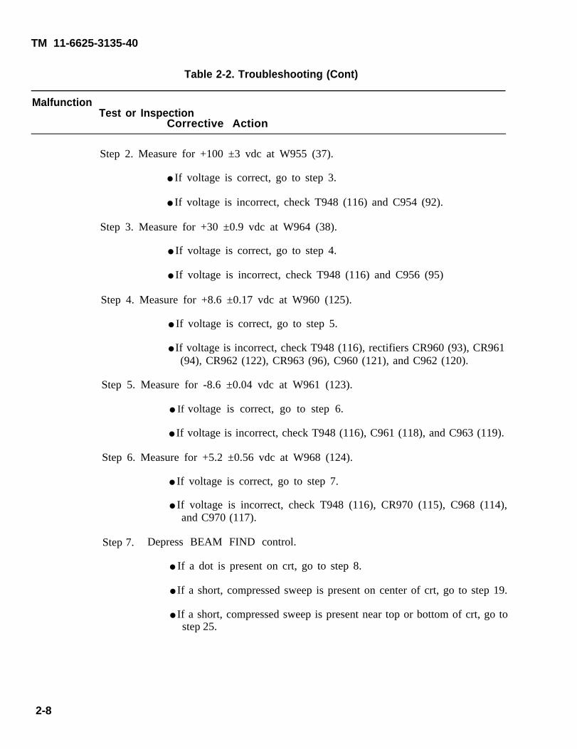
TM 11-6625-3135-40
Table 2-2. Troubleshooting (Cont)
MalfunctionTest or Inspection
Corrective Action
Step 2. Measure for +100 ±3 vdc at W955 (37).
If voltage is correct, go to step 3.
If voltage is incorrect, check T948 (116) and C954 (92).
Step 3. Measure for +30 ±0.9 vdc at W964 (38).
If voltage is correct, go to step 4.
If voltage is incorrect, check T948 (116) and C956 (95)
Step 4. Measure for +8.6 ±0.17 vdc at W960 (125).
If voltage is correct, go to step 5.
If voltage is incorrect, check T948 (116), rectifiers CR960 (93), CR961(94), CR962 (122), CR963 (96), C960 (121), and C962 (120).
Step 5. Measure for -8.6 ±0.04 vdc at W961 (123).
If voltage is correct, go to step 6.
If voltage is incorrect, check T948 (116), C961 (118), and C963 (119).
Step 6. Measure for +5.2 ±0.56 vdc at W968 (124).
If voltage is correct, go to step 7.
If voltage is incorrect, check T948 (116), CR970 (115), C968 (114),and C970 (117).
Step 7. Depress BEAM FIND control.
If a dot is present on crt, go to step 8.
If a short, compressed sweep is present on center of crt, go to step 19.
If a short, compressed sweep is present near top or bottom of crt, go tostep 25.
2-8

TM 11-6625-3135-40
Table 2-2. Troubleshooting (Cont)
MalfunctionTest or Inspection
Corrective Action
Step 8. Check for the following waveforms at W9705 (84) pin 2 and W9705 (84) pin 3.
E L9VP004
If either waveform is incorrect, go to step 9.
. If both waveforms are correct, go to step 11.
Step 9. Check for the following waveform at A4R707 ( 159).
If waveform is correct, go to step 10. EL9VP016
If waveform is incorrect, go to step 12.
Step 10. Measure a DISP voltage (+5 vdc) at A4P9700 ( 160) pin 1.
. If correct, replace A4 (para 2-20),
. If incorrect, go to step 16.
Step 11. Check for the following waveforms at W9788 (48) and W9778 (47).
. If both waveforms are correct, check crt wiring.
. If either waveform is incorrect, check horizontal output amplifierQ770 (24), Q775 (44), Q779 (43), Q780 (23), Q785 (20), Q789 (42), andassociated components.
2-9

TM 11-6625-3135-40
Table 2-2. Troubleshooting (Cont)
MalfunctionTest or Inspection
Corrective Action
Step 12. Check A GATE at A4P9700 (160) pin 8 and A SWP at A4P9700 pin 7 forhigh or low (pin 7 high is+ 12 vdc, low is +0.7 vdc; pin 8 high is + 1.5 vdc, low iszero).
If both are either high or low, replace A4 (para 2-20).
If one is high and the other low, go to step 13.
Step 13. Check W9001 (145) pin 25 for high or low.
If high, go to step 14.
If low. check A TRIGGER MODE switch S401 on A3 at pins 2 and 3for open, C505 (136) for short, and R505 (77) for open. If S401 isdefective, replace A3 (para 2-23); if not, replace defective component.
Step 14. Measure W9001 (146) pin 24 for approximately -8.3 •0.3 vdc.
❵ If voltage is not correct, replace A3 (para 2-23).
If voltage is correct, go to step 15.
Step 15. Measure W9001 (145) pin 30 for approximately +8.6 ±0.3 vdc.
If voltage is not correct, replace A3 (para 2-23).
• If voltage is correct, check A Sweep Generator Logic Circuitcomponents U502 (138), U504 (78), U506 (135), U532 ( 132), andassociated components.
Step 16. Check for high at J9400 pin 15 (88) (high is +5 vdc).
If high is present, check R566 (83).
If high is not present, check resistor R676 (82). If resistor is good, goto step 17.
Step 17. Check J9400 (28) pin 13 for low (low is zero).
If low, replace A5 (para 2-18).
If high, go to step 18.
2-10

TM 11-6625-3135-40
Table 2-2. Troubleshooting (Cont)
MalfunctionTest or Inspection
Corrective Action
Step 18. Check W9001 (148) pin 16 for low(low is zero).
If low, check A1 printed circuit between A1W9001A1J9400 pin 13.
If high, replace A3 (para 2-23).
Step 19. Check TP842 (33) for a pulse with
If present, go to step 20.
If not present, go to step 23.
an amplitude of 40-60V.
Step 20. Check for the following waveform at junction of R854 (98’
pin 15 and
and CR853 (99
V A R I E S W I T H INTENSITY SETTING
If incorrect, check GRIDcomponents.
EL9VP018
BIAS pot R851 (34) and associated
Step 21. Measure for approximately -2 kv at W9870 pins 1, 2, 3, and 14 (39).
If present, go to step 22. If not present, check U975 (91) and associated components.
Step 22. Measure for approximately -1500 vdc at W9870 pin 4 (40).
If present, replace crt (para 2-14). If not present, go to step 22a.
Step 22a. Check R888, R889, R890, R891, R892, and R894.
If faulty, replace all 6 resistors. If not faulty, check FOCUS pot R893 (41) and associated components.
Step 23. Check for the following waveform at Q825 (28) emitter.
EL9VP019
If not present, go to step 24.
If present, check Z-Axis circuit components Q829 (29), Q835 (31), Q840 (32), Q845 (30), and associated components.
Change 1 2-11

TM 11-6625-3135-40
Table 2-2. Troubleshooting (Cont)
MalfunctionTest or Inspection
Corrective Action
Step 24. Measure voltage at Q804 (69) emitter. Voltage should be +3 to -8 vdc,depending on position of intensity control.
If voltage is correct, replace A5 (para 2-18).
If not, check Q804 (69), Q586 (130), and associated components.
Step 25. Disconnect A3P9103.
If trace centers, replace A3 (para 2-23).
If trace does not center, reconnect A3P9103 and go to step 26.
Step 26. Measure for +0.7 vdc at U130 (63), pin 14.
If voltage is present, go to step 29.
If voltage is not present, go to step 27.
Step 27. Check for low at U540 pin 4 (26) (low is +0.7 vdc).
If pin 4 is low, check U540 (26), U537 (27), and associatedcomponents.
If pin 4 is not low, go to step 28.
Step 28. Check for low at A4P9250 pin 3 (162) (low is zero).
If pin 3 is low, replace A3 (para 2-23).
If pin 3 is not low, replace A4 (para 2-20).
Step 29. Measure for 0 volts at DL9210 (both + and - sides).
If no voltage is present, go to step 36.
If voltage is present, go to step 30.
Step 30. Measure for +2.7 ±0.1 vdc at base of Q202 (3) and Q203 (4).
If voltage is correct, check Q202 (3), Q203 (4), Q206 (2), Q207 (5),U225 (l), and associated components.
If voltage is not correct, go to step 31.
2-12
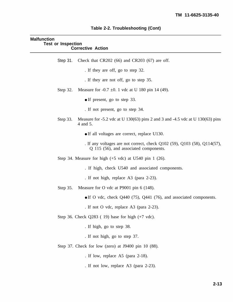
TM 11-6625-3135-40
Table 2-2. Troubleshooting (Cont)
MalfunctionTest or Inspection
Corrective Action
Step 31. Check that CR202 (66) and CR203 (67) are off.
. If they are off, go to step 32.
. If they are not off, go to step 35.
Step 32. Measure for -0.7 ±0. 1 vdc at U 180 pin 14 (49).
If present, go to step 33.
. If not present, go to step 34.
Step 33. Measure for -5.2 vdc at U 130(63) pins 2 and 3 and -4.5 vdc at U 130(63) pins4 and 5.
If all voltages are correct, replace U130.
. If any voltages are not correct, check Q102 (59), Q103 (58), Q114(57),Q 115 (56), and associated components.
Step 34. Measure for high (+5 vdc) at U540 pin 1 (26).
. If high, check U540 and associated components.
. If not high, replace A3 (para 2-23).
Step 35. Measure for O vdc at P9001 pin 6 (148).
If O vdc, check Q440 (75), Q441 (76), and associated components.
. If not O vdc, replace A3 (para 2-23).
Step 36. Check Q283 ( 19) base for high (+7 vdc).
. If high, go to step 38.
. If not high, go to step 37.
Step 37. Check for low (zero) at J9400 pin 10 (88).
. If low, replace A5 (para 2-18).
. If not low, replace A3 (para 2-23).
2-13

TM 11-6625-3135-40
Table 2-2. Troubleshooting (Cont)
MalfunctionTest or Inspection
Corrective Action
Step 38. Check for low (zero) at Q284 (16) base.
If low, go to step 39.
If not low, check Q283 (19) and associated components.
Step 39. Disconnect one end of R288 ( 15) and R289 ( 14).
If trace centers, check Q284 (16), Q285 ( 11), and associatedcomponents. Reconnect R288 and R289.
If trace does not center, go to step 40.
Step 40. Measure for +8.8 vdc at Q256 (22) and Q257 (21) collectors.
If correct, check crt wiring.
If not correct, check Q230 (12), Q231 (13), Q254 (18), Q255 (17),Q256 (22), Q257 (21), Q283 (19), Q284 (16), Q285 (1 1), and associatedcomponents.
3. NO VERTICAL DEFLECTION ON CHANNEL 1.
NOTE
Before performing troubleshooting, make sure all controls are set topositions listed in table 2-1.
Step 1. Measure for +8.6 ±0.2 vdc at A2P9991 (155) pin 1 and for -8.6 ±0.2 vdc atA2P9991 pin 3.
If voltage is correct, go to step 2.
If voltage is not correct, check wiring between A2P9991 (155) andA1 W9991.
Step 2. Apply 10 mv, 50 kHz signal to CH 1 OR X INPUT and check for signal atA2U30 pin 4 (154).
If signal is present, go to step 3.
If signal is not present, replace A2 (para 2-19).
2-14

TM 11-6625-3135-40
Table 2-2. Troubleshooting (Cont)
MalfunctionTest or Inspection
Corrective Action
Step 3. Measure for +4.8 ±0.1 vdc at A2P9103 (153) pins 2 and 3.
If voltage is correct, go to Malfunction 2 (steps 25-40).
If voltage is not correct, replace A2 (para 2-19).
4. NO VERTICAL DEFLECTION ON CHANNEL 2.
NOTE
Before performing troubleshooting, make sure all controls are set topositions listed in table 2-1.
Step 1. Measure for +8.6 ±0.2 vdc at A2P9991 (155) pin 1 and for -8.6 ±0.2 vdc atA2P9991 pin 3.
If voltage is correct, go to step 2.
If voltage is not correct, check wiring between A2P9991 (155) andA1W9991.
Step 2. Apply 10 mv, 50 kHz signal to CH 2 OR Y INPUT and check for signal atA2U80 pin 4 (158).
If signal is present, go to step 3.
If signal is not present, replace A2 (para 2-19).
Step 3. Measure for +4.8 ±0.1 vdc at A2P9108 (153) pins 2 and 3.
If voltage is correct, go to Malfunction 2 (steps 25-40).
If voltage is not correct, replace A2 (para 2-19).
2-15

TM 11-6625-3135-40
Table 2-2. Troubleshooting (Cont)
MalfunctionTest or Inspection
Corrective Action
5. INVERT FUNCTION FAULTY.
NOTE
Before performing troubleshooting, make sure all controls are set topositions listed in table 2-1.
Step 1. Measure for +2.5 ±0.1 vdc at A7P9200 pin 2 (151) and +3.4 ±0.2 vdc atA7W9200 pin 1 (150).
If voltage is correct, replace A2 (para 2-19).
If voltage is not correct, go to step 2.
Step 2. Check for +8.6 vdc at W9161-5 (149).
If present, replace A7 (para 2-24).
If not present, replace A3 (para 2-23).
6. CHANNEL 1 OR 2 DOES NOT CENTER VERTICALLY.
NOTE
Before performing troubleshooting, make sure all controls are set topositions listed in table 2-1.
Perform Malfunction 2 Troubleshooting, steps 25-40.
2-16

TM 11-6625-3135-40
Table 2-2. Troubleshooting (Cont)
MalfunctionTest or Inspection
Corrective Action
7. TRIG VIEW FUNCTION FAULTY.
NOTES
Before performing troubleshooting, make sure all controls are set topositions listed in table 2-1.
All measurements and checks must be done with TRIG VIEW switchheld in.
Step 1. Set Trig source to CH 1.Apply 10 mv, 50 kHz signal to CH 1 OR X INPUT.Measure for -8.6 ±0.2 vdc at W9001 pin 6 (148).
If present, go to step 2.
If not, replace A3 (para 2-23).
Step 2. Measure for -0.7 ±0.l vdc at U130 pin 14 (63) and U180 pin 14 (49) (U130 andU 180 should be off).
Step 3. Check
If correct, go to step 3.
If not, check R138 (62) and R188 (61).
that CR202 (66) and CR203 (67) are turned on.
If they are, go to step 4.
If not, check VR200 (60), CR200 (64), CR201 (65), CR202 (66), andCR203 (67).
Step 4. Measure for 100 mV or less at base of Q440 (75).
If correct, go to step 12.
If not correct, go to step 5.
2-17
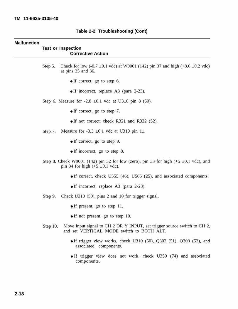
TM 11-6625-3135-40
Table 2-2. Troubleshooting (Cont)
MalfunctionTest or Inspection
Corrective Action
Step 5. Check for low (-0.7 ±0.1 vdc) at W9001 (142) pin 37 and high (+8.6 ±0.2 vdc)at pins 35 and 36.
If correct, go to step 6.
If incorrect, replace A3 (para 2-23).
Step 6. Measure for -2.8 ±0.1 vdc at U310 pin 8 (50).
If correct, go to step 7.
If not correct, check R321 and R322 (52).
Step 7. Measure for -3.3 ±0.1 vdc at U310 pin 11.
If correct, go to step 9.
If incorrect, go to step 8.
Step 8. Check W9001 (142) pin 32 for low (zero), pin 33 for high (+5 ±0.1 vdc), andpin 34 for high (+5 ±0.1 vdc).
If correct, check U555 (46), U565 (25), and associated components.
If incorrect, replace A3 (para 2-23).
Step 9. Check U310 (50), pins 2 and 10 for trigger signal.
If present, go to step 11.
If not present, go to step 10.
Step 10. Move input signal to CH 2 OR Y INPUT, set trigger source switch to CH 2,and set VERTICAL MODE switch to BOTH ALT.
If trigger view works, check U310 (50), Q302 (51), Q303 (53), andassociated components.
If trigger view does not work, check U350 (74) and associatedcomponents.
2-18
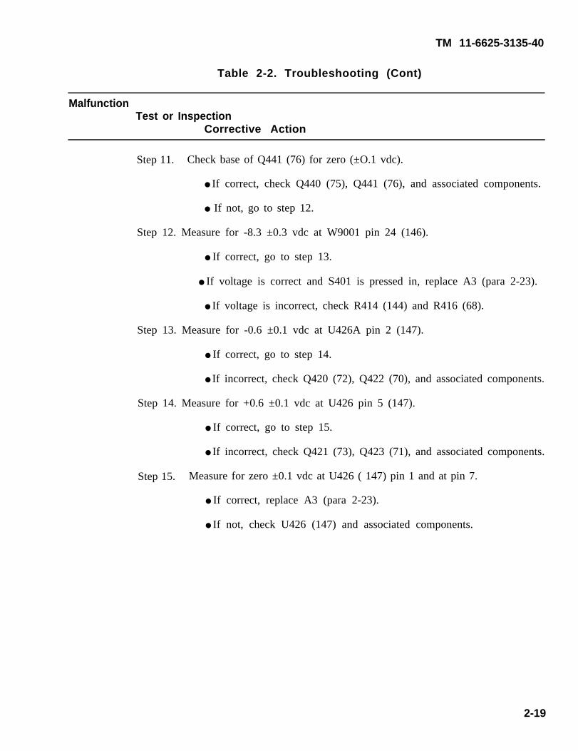
TM 11-6625-3135-40
Table 2-2. Troubleshooting (Cont)
MalfunctionTest or Inspection
Corrective Action
Step 11. Check base of Q441 (76) for zero (±O.1 vdc).
If correct, check Q440 (75), Q441 (76), and associated components.
If not, go to step 12.
Step 12. Measure for -8.3 ±0.3 vdc at W9001 pin 24 (146).
If correct, go to step 13.
If voltage is correct and S401 is pressed in, replace A3 (para 2-23).
If voltage is incorrect, check R414 (144) and R416 (68).
Step 13. Measure for -0.6 ±0.1 vdc at U426A pin 2 (147).
If correct, go to step 14.
If incorrect, check Q420 (72), Q422 (70), and associated components.
Step 14. Measure for +0.6 ±0.1 vdc at U426 pin 5 (147).
If correct, go to step 15.
If incorrect, check Q421 (73), Q423 (71), and associated components.
Step 15. Measure for zero ±0.1 vdc at U426 ( 147) pin 1 and at pin 7.
If correct, replace A3 (para 2-23).
If not, check U426 (147) and associated components.
2-19

TM 11-6625-3135-40
Table 2-2. Troubleshooting (Cont)
MalfunctionTest or Inspection
Corrective Action
8. VERTICAL BANDWIDTH FUNCTION FAULTY.
NOTES
Before performing troubleshooting, make sure all controls are set topositions listed in table 2-1.
This procedure is for channel 1. Channel 2 is the same except forreference designators.
Set up oscilloscope for band pass measurement.Apply signal to CH 1 OR X INPUT.Reverse A2P9103 (153) and A2P9108 (157). Set VERTICAL MODE to CH 2.
. If band pass is still faulty, replace A2 (para 2-19).
. If band pass is not still faulty, check Cl 30, C180, C210, C237, C250,and C251.
9. VERTICAL BANDWIDTH LIMIT FUNCTION FAULTY.
Before performing troubleshooting, make sure all controls are set topositions listed in table 2-1.
Press in BW LIMIT switch.Measure for +8.6 ±0.2 vdc at W9OO1-10 (148).
. If not correct, replace A3 (para 2-23).
. If correct, check CR226 (6), CR227 (7), CR228 (9), CR229 (8), C228,C229, and associated components.
2-20

TM 11-6625-3135-40
Table 2-2. Troubleshooting (Cont)
MalfunctionTest or Inspection
Corrective Action
10. HORIZONTAL TIMING INACCURATE.
NOTE
Before performing troubleshooting, make sure all controls are set topositions listed in table 2-1.
Step 1. Monitor A4R701 (161) pin 1 for approximately -8 vdc ±50 mv, as switch isturned through all TIMING ranges.
If voltage varies more than 5 mV, replace A4 (para 2-20).
11. POOR HORIZONTAL LINEARITY.
NOTE
Before performing troubleshooting, make sure all controls are set topositions listed in table 2-1.
Check horizontal linearity of both A and B sweeps.
If both are bad, replace crt (para 2-14).
If one is bad, replace A4 (para 2-20).
2-21

TM 11-6625-3135-40
Table 2-2. Troubleshooting (Cont)
MalfunctionTest or Inspection
Corrective Action
12. SWEEP SEPARATION FAULTY.
NOTE
Before performing troubleshooting, make sure all controls are set topositions listed in table 2-1.
Step 1. Set HORIZ mode to ALT.Set B trigger level to RUNS AFTER DELAY.
Step 2. Check for the following waveform at W282 (45).
If correct, go to step 3.
If not correct, go to step 6.
Step 3. Check that W9001 (55), pin 4 goes from +8.6 to 0 to 8.6 vdcwhen A/ BSWP SEP control is turned from clockwise to counter-clockwise.
If correct, go to step 4.
If not correct, - A/B SWP SEP control is defective;replace A3 (para 2-23).
Step 4. Set A/B SWP SEP control to clockwise position.Check Q284 (16) base for +0.3 vdc when waveform in step 2 islow and 0 when waveform in step 2 is high.
If correct, go to step 5.
If not correct, check Q283 (11), Q284 (16), andassociated components.
2-22

TM 11-6625-3135-40
Table 2-2. Troubleshooting (Cont)
MalfunctionTest or Inspection
Corrective Action
Step 5. Check base of Q285 (11) for low.
If correct, check Q285 (11) and associated components.
If not correct, replace R285 (10).
Step 6. Check J9400 pin 10 (88) for high.
If correct, replace A5 (paragraph 2-18).
If not correct, go to step 7.
Step 7. Disconnect one end of C647 (87) and check W9001 pin 27 (145) for high.
If correct, check C647 (87) and R649 (133).
If not correct, replace A3 (para 2-23) and reconnect C647.
13. B TIME DELAY RANGE FAULTY.
N O T E
Before performing troubleshooting, make sure all controls are set topositions listed in table 2-1.
Step 1. Set HORIZ MODE to ALT.Set B trigger level to RUNS AFTER DELAY.
Step 2. Check J9400 (88) pin 14 for +6.2 to less than +1.0 vdc as B DELAY TIMEPOSITION control is rotated from stop to stop.
If correct, go to step 3.
If incorrect, check B DELAY TIME POSITION control, R646 (131),C646 (126), and R647 (127).
2-23

TM 11-6625-3135-40
Table 2-2. Troubleshooting (Cont)
MalfunctionTest or Inspection
Corrective Action
Step 3. Check for following waveform at J9400-20 (88).
If incorrect, go to Malfunction 2, steps 9-18.
Step 4. Measure J9400 pin 13 (88) for +5 vdc.
If correct, go to step 6.
If incorrect, go to step 5.
Step 5. Check continuity from W9100 pin 15 (148) to ground.
If continuity is there, replace A3 (para 2-23).
If no continuity, check R648 (134) and C648 (128).
Step 6. Check for following waveform at J9400 pin 21 (88).
If not correct, go to Malfunction 2, steps 9-18.
Step 7. Check J9400 pin 4 (88) for +8.6 ±0.2 vdc.
If correct, go to step 8.
If not correct, replace A3 (para 2-23).
2-24

TM 11-6625-3135-40
Table 2-2. Troubleshooting (Cont)
MalfunctionTest or Inspection
Corrective Action
Step 8. Check for following waveforms at J9400 pin 22 (88) and J9400 pin 22 (88).
If correct, replace A5 (para 2-18).
If not correct (both high or low at the same time), replace A4 (para 2-20).
14. TRACE DOES NOT ENTER HORIZONTALLY.
NOTE
Before performing troubleshooting, make sure all controls are set topositions listed in table 2-1.
Step 1. Check for following waveforms at A4P9705 (164) pins 2 and 3.
A4P9705-2
A4P9705-3
EL9VP038
If correct, go to step 3.
If not correct, go to step 2.
2-25
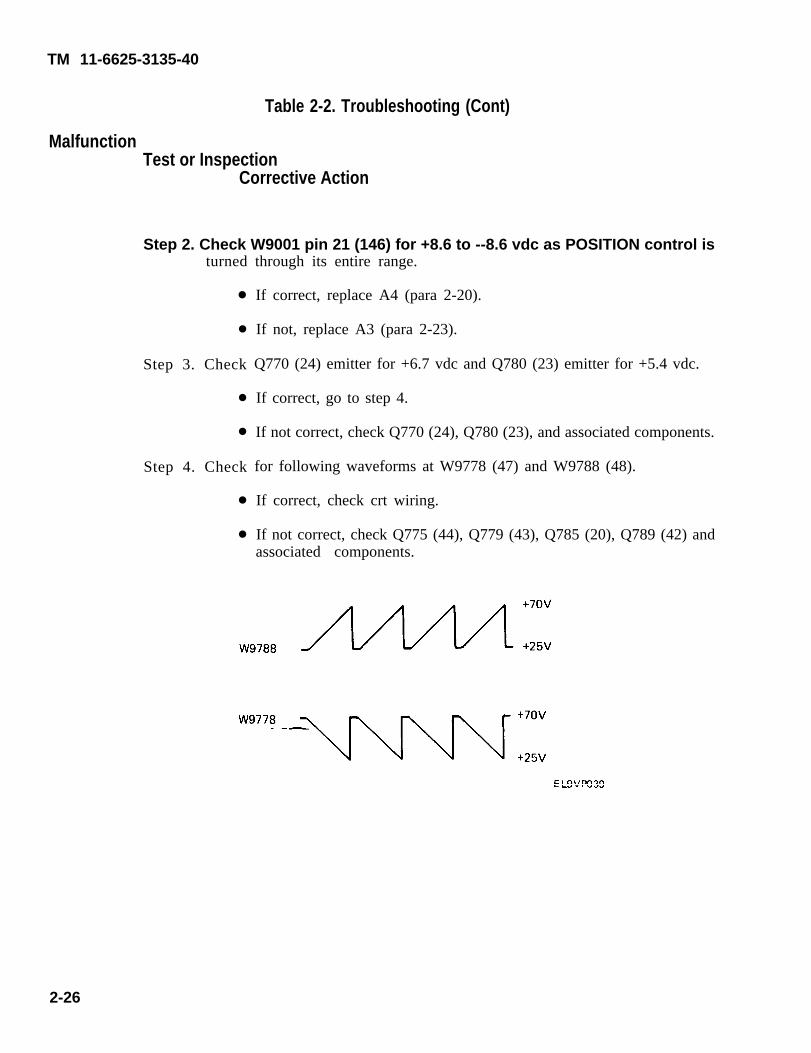
TM 11-6625-3135-40
Table 2-2. Troubleshooting (Cont)
MalfunctionTest or Inspection
Corrective Action
Step 2. Check W9001 pin 21 (146) for +8.6 to --8.6 vdc as POSITION control isturned
Step 3. Check
Step 4. Check
through its entire range.
If correct, replace A4 (para 2-20).
If not, replace A3 (para 2-23).
Q770 (24) emitter for +6.7 vdc and Q780 (23) emitter for +5.4 vdc.
If correct, go to step 4.
If not correct, check Q770 (24), Q780 (23), and associated components.
for following waveforms at W9778 (47) and W9788 (48).
If correct, check crt wiring.
If not correct, check Q775 (44), Q779 (43), Q785 (20), Q789 (42) andassociated components.
2-26

TM 11-6625-3135-40
Table 2-2. Troubleshooting (Cent)
MalfunctionTest or Inspection
Corrective Action
15. LOW X GAIN.
NOTE
Before performing troubleshooting, make sure all controls are set topositions listed in table 2-1.
Step 1. Set A AND B SEC/ DIV switch to X-Y.Connect 10 mv square wave signal to CH 1 OR X.
Step 2. Check A4U760 pin 11 (163) for approximately 200 mv square wave.
. If correct, replace A4 (para 2-20).
. If not correct, check U758 (81), Q756 (79), and associated components.
16. IMPROPER SWEEP LENGTH.
NOTE
Before performing troubleshooting, make sure all controls are set topositions listed in table 2-1.
Step 1. Check for following waveform at A4R707 (159).
2-27

TM 11-6625-3135-40
Table 2-2. Troubleshooting (Cent)
MalfunctionTest or Inspection
Corrective Action
Step 2. Check for following waveforms at A4P9705 pins 2 and 3 ( 164),
Step 3. Check for following waveform at U504-9 (78).
. If correct, check R525 (85), C525 (129), Q525 (80), R524 (86), andassociated components.
. If not correct, check U504 (78) and associated components.
2-28
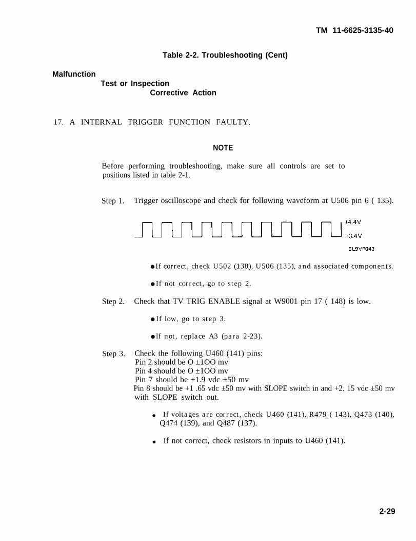
TM 11-6625-3135-40
Table 2-2. Troubleshooting (Cent)
MalfunctionTest or Inspection
Corrective Action
17. A INTERNAL TRIGGER FUNCTION FAULTY.
NOTE
Before performing troubleshooting, make sure all controls are set topositions listed in table 2-1.
Step 1.
Step 2.
Step 3.
Trigger oscilloscope and check for following waveform at U506 pin 6 ( 135).
If correct, check U502 (138), U506 (135), and associated components.
If not correct, go to step 2.
Check that TV TRIG ENABLE signal at W9001 pin 17 ( 148) is low.
If low, go to step 3.
lf not, replace A3 (para 2-23).
Check the following U460 (141) pins:Pin 2 should be O ±1OO mvPin 4 should be O ±1OO mvPin 7 should be +1.9 vdc ±50 mvPin 8 should be +1 .65 vdc ±50 mv with SLOPE switch in and +2. 15 vdc ±50 mvwith SLOPE switch out.
. If voltages are correct, check U460 (141), R479 ( 143), Q473 (140),Q474 (139), and Q487 (137).
. If not correct, check resistors in inputs to U460 (141).
2-29

TM 11-6625-3135-40
Table 2-2. Troubleshooting (Cent)
MalfunctionTest or Inspection
Corrective Action
18. B INTERNAL TRIGGER FUNCTION FAULTY.
NOTE
Before performing troubleshooting, make sure all controls are set topositions listed in table 2-1.
Step 1. Check A trigger function.
If it is correct, go to step 2.
If not, go to malfunction 17.
Step 2. Check that J9400-4 (88) voltage is +8.6 ±0.2 vdc to -8.6 ±O.2 vdc when BTRIGGER LEVEL control is rotated through its range.
If correct, go to step 3.
If not, replace A3 (para 2-23).
Step 3. Check voltage at A5U605 pin 8 (152). It should be +1.65 vdc ±50 mv withSLOPE switch in, and +2.15 vdc ±5O mv with SLOPE switch out.
If correct, replace A5 (para 2-18).
If not, replace A3 (para 2-23).
19. FOCUS DOES NOT WORK.
Go to Malfunction 2 (steps 21 and 22).
2-30
TM 11-6625-3135-40
Table 2-2. Troubleshooting (Cent)
MalfunctionTest or Inspection
Corrective Action
20. TRACE DRIFTS.
Before performing troubleshooting, make sure all controls are set topositions listed in table 2-1.
This procedure is for channel 1. Channel 2 is the same except forreference designators.
Reverse A2P9103 (153) and A2P9108 (157).
If trace still drifts, check U130 (63), Q102 (59), Q102 (59), Q103 (58),Q114 (57), Q115 (56), and associated components.
If trace does not drift, replace A2 (para 2-19).
21. X10 MAGNIFIER DOES NOT WORK.
CAUTION
Make sure power to oscilloscope is off to prevent damage to multimeter.
With power off and X 10 magnifier switch closed (pulled out), check for continuitybetween A8W9726 (166) and A8W9724 (167).
If continuity exists, replace A4 (para 2-20).
If continuity does not exist, replace A8 (para 2-21).
2-31

TM 11-6625-3135-40
2-12. POWER SUPPLY FAULT ISOLATION TEST
DESCRIPTION
This test locates the faulty power supply component.
INITIAL SETUP
With cover removed, several dangerous voltage points may be exposed.Contact with these points could cause serious injury or death.
The oscilloscope power source must be connected through an isolationtransformer or damage to equipment could result.
All measurements and waveforms are to chassis ground unlessotherwise noted.
All reference designations are on A 1 unless otherwise noted.
All test point locations in ( ) are located on fig. FO-1.
NOTE
After replacing failed part, do functional check to verify original faulthas been corrected.
1. Set all controls to positions listed in table 2-1.
2. Check for +43 ±1 vdc between TP940 ( 109) and TP950 (105) (ground).
If voltage is incorrect, go to step 3.
If voltage is correct, go to step 4.
2-32

TM 11-6625-3135-40
2-12. POWER SUPPLY FAULT ISOLATION TEST (CONT)
3. Check for the foIlowing waveform at U930, pin IO ( 106).
If waveform is correct, check Q928, Q930, Q908, Q907, and assorted components.
If waveform is incorrect, go to step 5.
4. Check for the following waveform at R949 (111).
If waveform is incorrect, go to step 5.
If waveform is correct, go to step 6.
5. Disconnect one end of R949 (111 ) and check for +43 ±1 vdc between TP940 ( 109) and TP950( 105) (ground).
If voltage is correct, reconnect R949 and go to step 6.
If voltage is incorrect, check Q938 (110), Q939 (108), Q944 (107), Q946 (113), Q947 (112), andtheir associated components. Replace defective component and reconnect R949.
6. Disconnect wire between T948 (116) and U975 (91), and check if POWER indicator DS901comes on.
If POWER indicator comes on, check U975 or associated components. Replace defectivecomponent and reconnect wire.
If POWER indicator does not come on, reconnect wire and go to step 7.
7. Disconnect jumpers W955 (37) and W954 (90) (+100 vdc supply) and check if POWER indicatorcomes on.
If POWER indicator comes on, trace +100 vdc distribution (fig. FO-12), replace defectivecomponent, and reconnect jumpers.
If POWER indicator does not come on, go to step 11.
2-33
TM 11-6625-3135-40
2-12. POWER SUPPLY FAULT ISOLATION TEST (CONT)
8. Check C954 (92) for short.
If shorted, replace C954 and reconnect jumpers.
If C954 is not shorted, reconnect jumpers and go to step 9.
9. Disconnect jumpers W956 (89) and W964 (38) (+30 vdc supply) and check if POWER indicatorcomes on.
If POWER indicator comes on, trace +30 vdc distribution (fig. FO-12), replace defectivecomponent, and reconnect jumpers.
If POWER indicator does not come on, go to step 10.
10, Check C956 (95) for short.
If shorted, replace C956 and reconnect jumpers,
If C956 is not shorted, reconnect jumpers and go to step 11.
11. Disconnect jumper W960 (125) (+8.6 vdc supply) and check if POWER indicator comes on.
If POWER indicator comes on, trace +8.6 vdc distribution (fig. FO-12), replace defectivecomponent and reconnect jumper.
If POWER indicator does not come on, go to step 12.
12. Check C960 (125) and C962 (120) for short.
If shorted, replace defective capacitor and reconnect jumper.
If neither capacitor is shorted, reconnect jumper and go to step 13.
13. Disconnect jumper W961 (123) ( 8.6 vdc supply) and check if POWER indicator comes on.
If POWER indicator comes on, trace -8.6 vdc distribution (fig. FO-12), replace defectivecomponent and reconnect jumper.
If POWER indicator does not come on, go to step 14.
14. Check C961 (118) and C963 (119) for short.
If shorted, replace defective component and reconnect jumper.
If neither capacitor is shorted, reconnect jumper and go to step 15.
2-34

TM 11-6625-3135-40
2-12. POWER SUPPLY FAULT ISOLATION TEST (CONT)
15. Disconnect jumper W968 (124) and resistor R964 (36) (+5.2 vdc supply) and check for +5.2±O.l6vdc between C970 (117) and chassis ground.
If voltage is correct, trace +5.2 vdc distribution (fig. FO-12), replace defective component, andreconnect jumper and resistor.
If POWER voltage is correct, check capacitors C968 (114) and C970 (117) for short.Reconnect jumper and resistor.
END OF TASK
2-35

TM 11-6625-3135-40
Section IV. MAINTENANCE PROCEDURES
2-13. CABINET REMOVAL
DESCRIPTION
This procedure covers: Remove and Install
To avoid electrical shock, disconnect oscilloscope from ac power sourcebefore removing or replacing any component or assembly.
REMOVE
1. Disconnect power cord and accessories from oscilloscope.
2. Remove screws at right rear side (1), bottom front (2), and rear panel (3). Remove rear panel (4).
3. Pull chassis (5) forward and out of cabinet (6). 3
2-36
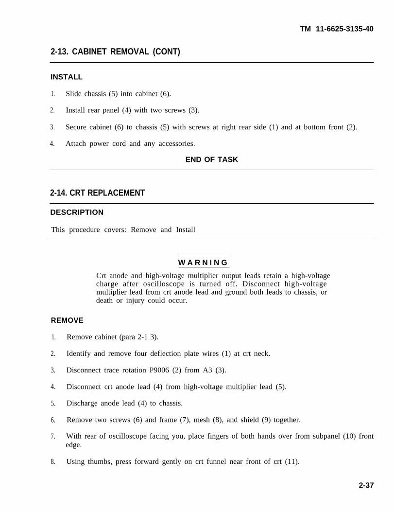
TM 11-6625-3135-40
2-13. CABINET REMOVAL (CONT)
INSTALL
1. Slide chassis (5) into cabinet (6).
2. Install rear panel (4) with two screws (3).
3. Secure cabinet (6) to chassis (5) with screws at right rear side (1) and at bottom front (2).
4. Attach power cord and any accessories.
END OF TASK
2-14. CRT REPLACEMENT
DESCRIPTION
This procedure covers: Remove and Install
W A R N I N G
Crt anode and high-voltage multiplier output leads retain a high-voltagecharge after oscilloscope is turned off. Disconnect high-voltagemultiplier lead from crt anode lead and ground both leads to chassis, ordeath or injury could occur.
REMOVE
1.
2.
3.
4.
5.
6.
7.
8.
Remove cabinet (para 2-1 3).
Identify and remove four deflection plate wires (1) at crt neck.
Disconnect trace rotation P9006 (2) from A3 (3).
Disconnect crt anode lead (4) from high-voltage multiplier lead (5).
Discharge anode lead (4) to chassis.
Remove two screws (6) and frame (7), mesh (8), and shield (9) together.
With rear of oscilloscope facing you, place fingers of both hands over from subpanel (10) frontedge.
Using thumbs, press forward gently on crt funnel near front of crt (11).
2-37

TM 11-6625-3135-40
2-14. CRT REPLACEMENT (CONT).
9. When crt base pins disengage from socket ( 12), remove crt (11) and crt shield ( 13) through frontsubpanel (10).
10. Place crt (11) in safe place for installation.
11. If corner pads (14) fall out, save them for installation.
12. Remove two nuts (15) and crt cover ( 16).
2-38

TM 11-6625-3135-40
2-14. CRT REPLACEMENT (CONT)
INSTALL
1.
2.
3.
4.
5.
6.
7.
8.
9.
10.
11.
Install corner pads ( 14).
Ensure crt (11) pins are straight.
Insert crt shield (13) and crt (11) through front subpanel (10).
Ensure crt shield ( 13) and base socket (12) index keys are aligned.
Carefully align and seat crt (11) pins with socket ( 12).
Install crt cover (16) and two nuts (1 5).
Assemble shield (9), mesh (8), and crt frame (7), then install and secure with two screws (6).
Connect crt anode lead (4) to high-voltage multiplier lead (5).
Connect P9006 (2) to A3 (3).
Connect four deflection plate wires (1) to crt neck.
Install cabinet (para 2-1 3).
END OF TASK
2-15. A10 SCALE ILLUMINATION CIRCUIT BOARD ASSEMBLY REPLACEMENT
DESCRIPTION
This procedure covers: Remove and Install
REMOVE
1. Remove cabinet (para 2-13).
2. Disconnect P9882 (1) from A1O (2).
3. Remove two screws (3), frame (4), mesh (5), and shield (6) together.
4. Remove screw (7), eyelet, A 10 (2), and light reflector (8).
2-39

TM 11-6625-3135-40
2-15. A10 SCALE ILLUMINATION CIRCUIT BOARD ASSEMBLY REPLACEMENT (CONT)
INSTALL
1. Install light reflector (8), eyelet, and A10 (2) with screw (7).
2. Assemble shield (6), mesh (5), and frame (4). Secure with two screws (3),
3. Attach P9882 (1) to A10 (2).
4. Install cabinet (paragraph 2-13).
END OF TASK
2-40

TM 11-6625-3135-40
2-16. POWER SUPPLY SHIELD REMOVAL
DESCRIPTION
This procedure covers: Remove and Install
REMOVE
1. Remove cabinet (para 2-13).
2. Remove screw ( 1). Press gently on rear of cover (2) and slide it forward.
3. Remove A5 (para 2-18).
4. Remove five screws (3). Remove crt anode lead from clip (4).
5. Lift shield (5) out of chassis (6) by tilting right rear corner up.
2-41

TM 11-6625-3135-40
2-16. POWER SUPPLY SHIELD REMOVAL (CONT)
INSTALL
1. Set shield (5) down and into chassis (6).
2. Install crt anode lead to clip (4). Install all five screws (3) loosely, then tighten.
3. Install A5 (para 2-18).
4. Press on front of cover (2) and slide it rearward. Install screw (1).
5. Install cabinet (para 2-1 3).
END OF TASK
2-17. A6 EMI FILTER CIRCUIT BOARD ASSEMBLY REPLACEMENT
DESCRIPTION
This procedure covers: Remove and Install
REMOVE
1.
2.
3.
4.
Remove cabinet (para 2-13) and power supply shield (para 2-16).
Pull off cover (l).
CAUTION
Cap (2) must be slid off fuseholder (3) before wires are unsoldered, ordamage to the cap could occur.
Slide cap (2) off fuseholder (3) and unsolder two wires from A1 (4), one from line filter (5), andone from fuseholder (3).
Remove two screws (6) and lift off A6 (7), with two nuts (8) and spacers (9) attached.
2-42

TM 11-6625-3135-40
2-17. A6 EMI FILTER CIRCUIT BOARD ASSEMBLY REPLACEMENT (CONT)
1. Install A6 (7) with two nuts (8), spacers (9), and screws (6).
2. Solder two wires from A 1 (4), one from line filter (5), and one from fuseholder (3). Slide cap (2)on fuseholder after soldering.
3. Install cover ( 1).
4. Install power supply shield (para 2-16) and cabinet (para 2-13),
END OF TASK
2-43

TM 11-6625-3135-40
2-18. A5 ALTERNATE SWEEP CIRCUIT BOARD ASSEMBLY REPLACEMENT
DESCRIPTION
This procedure covers: Remove and Install
REMOVE
1. Remove cabinet (para 2-13).
2. Unclip A5 (1) from holder (2) on shield (3).
3. Pull A5 (1) up and from Al connector (4).
INSTALL
1. Align A5 (1) with Al connector (4) and seat firmly.
2. Clip A5 (1) into holder (2) on shield (3).
3. Install cabinet (para 2-1 3).
END OF TASK
2-44

TM 11-6625-3135-40
2-19. A2 ATTENUATOR CIRCUIT BOARD ASSEMBLY REPLACEMENT
DESCRIPTION
This procedure covers: Remove and Install
REMOVE
1.
2.
3.
4.
5.
6.
7.
8.
9.
Remove cabinet (para 2-13).
Place oscilloscope on side and unsolder resistors (1) from CH 1 OR X and CH 2 OR Y inputconnectors (2).
Remove two screws (3) from bracket (4).
Loosen CH 1 and CH 2 VOLTS/ DIV variable knob setscrews (5) and remove knobs (6).
Set CH 1 and CH 2 VOLTS/ DIV switches to same setting and note for installation. Removeknobs (7) by pulling them straight from front panel.
Disconnect P9103 (8), P9108 (9), P9091 (10), P9405 (11), and P9200 ( 12).
Remove two screws (13), screw (14), screw (15), and shield (16).
Remove screw (17) and ground strap (18).
Remove screw (19) and pull A2 (20) straight back until switch shafts are clear.
2-45

TM 11-6625-3135-40
2-19. A2 ATTENUATOR CIRCUIT BOARD ASSEMBLY REPLACEMENT (CONT)
INSTALL
1. Position resistors (1) so leads will be accessible from bottom of oscilloscope after A2 (20) isinstalled.
2. Insert A2 (20).
3. Install screw (19), ground strap (18), and screw (17).
4. Install shield (16) and four screws (13, 14, and 15).
5. Install P9200 (12), P9405 ( 11), P9091 (10), P9108 (9) and P9103 (8).
6. Install switch knobs (7).
7. Install knobs (6) and tighten setscrews (5).
2-46

TM 11-6625-3135-40
2-19. A2 ATTENUATOR CIRCUIT BOARD ASSEMBLY REPLACEMENT (CONT)
8. Install two screws (3) in bracket (4). Tighten securely.
9. Solder resistors (1) to CH 1 OR X and CH 2 OR Y input connectors (2).
10. Install cabinet (para 2-13).
END OF TASK
2-20. A4 TIMING CIRCUIT BOARD ASSEMBLY REPLACEMENT
DESCRIPTION
This procedure covers: Remove and Install
1.
2.
3.
4.
5.
6.
7.
8.
Remove cabinet (para 2-13).
Loosen setscrew (1) and remove knob (2).
Lock A and B SEC/ DIV knobs (4 and 6) together in XY position.
Loosen two setscrews (3) and remove knob (4).
Loosen two setscrews (5) and remove knob (6).
Remove P9705 (7), P9700 (8), and P9723 (9).
Remove screw (10) securing ground strap.
Remove three screws (12) and pull A4 (13) back until pins disengage and switch shaft is clear offront panel.
2 - 4 7
REMOVE

TM 11-6625-3135-40
2-20. A4 TIMING CIRCUIT BOARD ASSEMBLY REPLACEMENT (CONT)
INSTALL
1. Insert A4 (13) by aligning switch shaft through front panel and engaging interconnecting pins.
2. Secure A4 (13) with three screws (12).
3. Install ground strap (11) and secure with screw (10).
4. Connect P9723 (9), P9700 (8) and P9705 (7).
5. Install knob (6) in XY position and tighten two setscrews (5).
6. Install knob (4) in XY position and tighten two setscrews (3).
7. Install knob (2) and tighten setscrew (1).
8. Install cabinet (para 2-13).
END OF TASK
2-48

TM
2-21. A8 TIMING POT CIRCUIT BOARD ASSEMBLY REPLACEMENT
11-6625-3135-40
DESCRIPTION
This procedure covers: Remove and Install
REMOVE
1. Remove cabinet (para 2-13) and A4 (para 2-20).
2. Unsolder wire W9722 (1) and wire (2) on A8 (3).
3. Unsolder two bus conductors (4) and leads (5).
4. Loosen setscrew (7).
5. Remove nut (6) and A8 (3) from A4 (8).
2 - 4 9
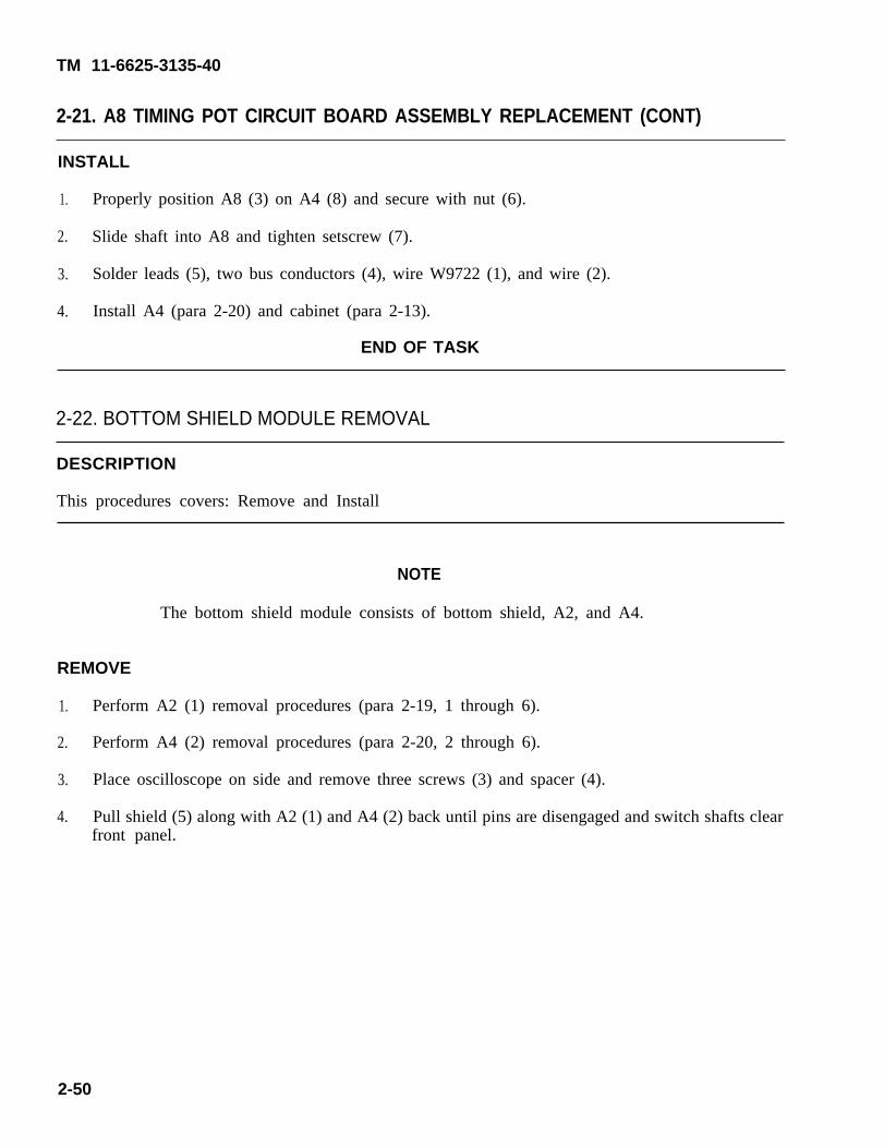
TM 11-6625-3135-40
2-21. A8 TIMING POT CIRCUIT BOARD ASSEMBLY REPLACEMENT (CONT)
INSTALL
1. Properly position A8 (3) on A4 (8) and secure with nut (6).
2. Slide shaft into A8 and tighten setscrew (7).
3. Solder leads (5), two bus conductors (4), wire W9722 (1), and wire (2).
4. Install A4 (para 2-20) and cabinet (para 2-13).
END OF TASK
2-22. BOTTOM SHIELD MODULE REMOVAL
DESCRIPTION
This procedures covers: Remove and Install
NOTE
The bottom shield module consists of bottom shield, A2, and A4.
REMOVE
1. Perform A2 (1) removal procedures (para 2-19, 1 through 6).
2. Perform A4 (2) removal procedures (para 2-20, 2 through 6).
3. Place oscilloscope on side and remove three screws (3) and spacer (4).
4. Pull shield (5) along with A2 (1) and A4 (2) back until pins are disengaged and switch shafts clearfront panel.
2-50
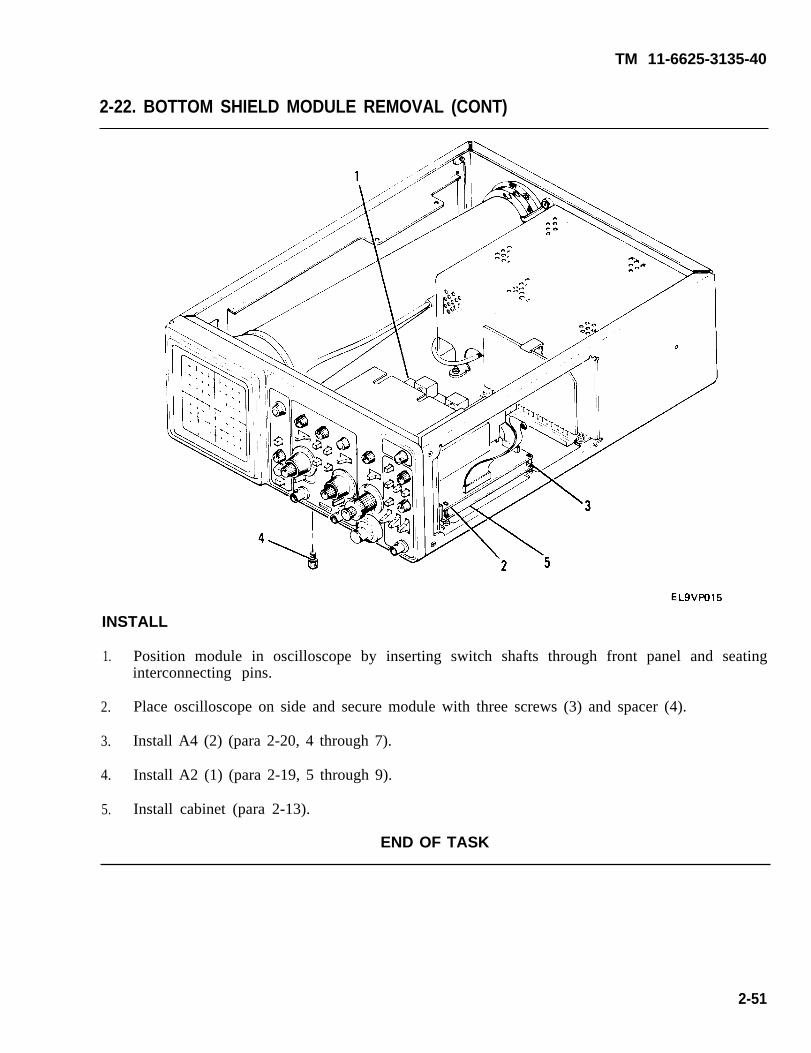
TM 11-6625-3135-40
2-22. BOTTOM SHIELD MODULE REMOVAL (CONT)
INSTALL
1. Position module in oscilloscope by inserting switch shafts through front panel and seatinginterconnecting pins.
2. Place oscilloscope on side and secure module with three screws (3) and spacer (4).
3. Install A4 (2) (para 2-20, 4 through 7).
4. Install A2 (1) (para 2-19, 5 through 9).
5. Install cabinet (para 2-13).
END OF TASK
2-51

TM 11-6625-3135-40
2-23. A3 FRONT PANEL CIRCUIT BOARD ASSEMBLY REPLACEMENT
REMOVE
1.
2.
3.
4.
5
6.
7.
8.
9.
10.
11.
12.
13.
14.
15.
16.
Remove cabinet (para 2-13), crt (para 2-14), and bottom shield module (para 2-22).
Pull six knobs (1).
Loosen setscrew (2) and remove knob (3), nut (4), and washer (5).
Pull FOCUS pot shaft (6) and remove from front panel.
Unsolder resistor (7), wire strap (8), AMP CAL lead (9) at A3 (10) (located between front paneland A3), and VAR HOLDOFF wires (11) at potentiometer.
Disengage POWER indicator DS9150 (12) from front panel.
Disconnect P9802 (13) and W9644 (14) from A1.
Disconnect P9882 (15) from A10.
Set front panel switches to center position.
Remove three screws (16) from A3, two screws (17) from chassis, two screws ( 18) from Al, onescrew (19) from delay line, and two screws (20) at right front corner.
Pull front-left frame (21) from chassis.
Unsolder leads (22) from W9409 (located on back of A3).
Unsolder 39 wire straps (23) (located between A1 and A3).
Unsolder W9881 (24) (located on front of A3).
Remove A3 (10). Clean wire strap holes in Al.
Remove A7 (25) (para 2-24).
2-52

TM 11-6625-3135-40
2-23. A3 FRONT PANEL CIRCUIT BOARD ASSEMBLY REPLACEMENT (CONT)
EL9VP046
2-53

TM 11-6625-3135-40
2-23. A3 FRONT PANEL CIRCUIT BOARD ASSEMBLY REPLACEMENT (CONT)
INSTALL
1.
2.
3.
4.
5.
6.
7.
8.
9.
10.
11.
12.
13.
14.
15.
Install A7 (25) on A3 (10) (para 2-24).
Position A3 (10) on Al and solder 39 wire straps (23).
Solder W9881 (24) to front of A3 (10).
Solder W9409 to back of A3.
Position front-left assembly (18) with chassis.
Install two screws (20) at right front corner, screw ( 19) at delay line, two screws ( 18) at A 1, twoscrews (17) at left rear corner, and three screws (16) at front panel.
Connect P9882 (15) to A1O.
Connect P9802 (13) and W9644 (14) to Al.
Insert POWER indicator DS9150 (12) in front panel.
Solder resistor (7), wire strap (8), and AMP CAL lead (9) to A3 (between A3 and front panel.
Solder wires (11) to VAR HOLDOFF pot.
Insert FOCUS pot shaft (6) through front panel and connect to pot.
Install washer (5), nut (4), and knob (3). Tighten setscrew (2).
Install six knobs (l).
Install bottom shield module (para 2-22), crt (para 2-14), and cabinet (para 2-13).
END OF TASK
2-54
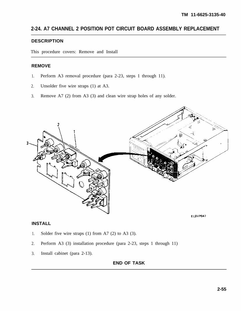
TM 11-6625-3135-40
2-24. A7 CHANNEL 2 POSITION POT CIRCUIT BOARD ASSEMBLY REPLACEMENT
DESCRIPTION
This procedure covers: Remove and Install
REMOVE
1. Perform A3 removal procedure (para 2-23, steps 1 through 11).
2. Unsolder five wire straps (1) at A3.
3. Remove A7 (2) from A3 (3) and clean wire strap holes of any solder.
INSTALL
1. Solder five wire straps (1) from A7 (2) to A3 (3).
2. Perform A3 (3) installation procedure (para 2-23, steps 1 through 11)
3. Install cabinet (para 2-13).
END OF TASK
2-55

TM 11-6625-3135-40
2-25. Al MAIN CIRCUIT BOARD ASSEMBLY REPLACEMENT
DESCRIPTION
This procedure covers: Remove and Install
REMOVE
1.
2.
3.
4.
5.
6.
7.
8.
9.
10.
11.
12.
13.
14.
15.
Remove cabinet (para 2-13).
Disconnect P9644 (1) from Al (2).
Remove pcb A5 (para 2-18) and power supply shield (para 2-16).
Unsolder two wires from A6 at W9190 (3) and W9040 (4).
Disconnect cables that go between A1 and A2, and between A1 and A4. Note locations.
Disconect P9802 (5).
Pull focus shaft (6) straight out from front panel.
Disengage POWER LED (7) from front panel.
Press POWER switch (8) to ON. Insert a scribe or similar tool into notch between end of switchshaft (9) and extension (10) and gently pry apart. Push extension ( 10) forward, then sideways toclear shaft (9), then pull extension back and out.
Unsolder wire W9800 (11) from EXT Z AXIS INPUT BNC connector located on rear panel.
Remove two screws ( 12).
W A R N I N G
Crt anode and high-voltage multiplier output leads retain a high-voltagecharge after oscilloscope is turned off. Disconnect high-voltage multiplierlead from crt anode lead and ground both leads.
Carefully disconnect crt anode lead (13) and ground to chassis.
Disconnect horizontal and vertical deflection wires (14) from crt.
Unsolder two sets of socket wires (15). Note location for installation.
Unsolder two sets of delay line wires (16). Note location for installation.
2-56

TM 11-6625-3135-40
2-25. Al MAIN CIRCUIT BOARD ASSEMBLY REPLACEMENT (CONT)
16. Remove three screws (17) and spacer (18) at bottom shield (19) and three screws (20) at chassis.
17. Identify and unsolder two leads (21) at W941O and one lead (22) at W9880 on A1.
18. Unsolder 39 wire straps (23) (located between A1 and A3).
19. Push wire-strap connection end of A1 (2) down until clear of all strap ends. Remove A1 (2)through bottom of chassis.
2-57

TM 11-6625-3135-40
2-25. Al MAIN CIRCUIT BOARD ASSEMBLY REPLACEMENT (CONT)
INSTALL
1. Position Al (2) into bottom of chassis.
2. Solder 39 wire straps (23) to A1 (2) (located between Al and A3).
3. Solder two leads (22) at W9880 and one lead (21) at W941O.
4. Secure A 1 with three screws (20).
5. Secure shield (19) to Al with three screws (17) and spacer (18).
6. Solder two sets of wires (16) from delay line to Al.
7. Solder two sets of wires (15) from crt socket to Al.
8. Connect horizontal and vertical deflection wires (14) to crt.
9. Connect crt anode lead (13) to high-voltage multiplier lead.
2-58

TM 11-6625-3135-40
2-25. Al MAIN CIRCUIT BOARD ASSEMBLY REPLACEMENT (CONT)
10.
11.
12.
13.
14.
15.
16.
17.
18.
19.
20.
Secure heatsink assembly to chassis with two screws (12).
Solder wire W9800 (11) to EXT Z AXIS BNC connector located on rear panel.
Position extension ( 10) into front panel. Push extension forward, then sideways to line up withshaft (9). Snap extension and shaft together.
Insert POWER LED (7) into front panel.
Insert focus shaft (6) into front panel.
Connect cables that go from Al to A2 and from Al to A4.
Connect P9802 (5).
Solder two wires from A6 to A1 at W9190 (3) and W9040 (4).
Install power supply shield (para 2-16) and A5 (para 2-18).
Connect P9644 (1) to Al (2).
Install cabinet (para 2-13).
END OF TASK
2-59
TM 11-6625-3135-40
2-26. CLEANING
DESCRIPTION
This procedure covers: Cleaning
1.
2.
3.
4.
Unplug power cord and remove cabinet (para 2-13).
Use approved personal protective equipment (goggles/ face shield) whenusing compressed air. Provide protection from flying particles. Do notdirect airstream toward self or other personnel, as injury may result.
Use dry, low-pressure air (approximately 9 psi) to blow off dirt.
Remove any remaining dirt with soft-bristle brush or soft cloth dampened in a mild detergentand water solution. Use cotton-tipped applicator for cleaning in narrow spaces and on pcb’s.
Isopropyl alcohol is flammable and harmful to eyes, skin, and breathingpassages. Provide adequate ventilation. Keep ignition sources away,and wear protective clothing.
CAUTION
Use only isopropyl alcohol as a cleaning solution, especially aroundattenuator A2. Carbon-based solvents damage board material.
Clean the switch contacts by applying alcohol with a small camel hair brush. Do not usecotton-tip applicators for cleaning contacts.
END OF TASK
2-60

TM 11-6625-3135-40
2-27. PERFORMANCE TESTS
The performance tests are broken into five parts:
Initial Setup
Vertical Circuits Tests
Horizontal Circuits Tests
Trigger Circuits Tests
External Z-Axis and Amplitude Calibrator Circuits Tests
NOTES
. Each section of the performance tests must be done in order and intheir entirety to ensure correct control settings.
. Allow an inital 20 minute warm up period when performing the firsttest to ensure the equipment stabilizes.
2-61

TM 11-6625-3135-40
INITIAL SETUP
1. Plug oscilloscope ac power cord into 115 V ac source.
2. Press POWER ON/OFF switch to ON and allow at least 20 minutes for oscilloscope to warm upand stabilize before first test.
3. Set oscilloscope controls as follows:
Control
l Vertical (Both Channels)POSITIONINVERTVERTICAL MODETRIGGER SOURCEBW LIMITVOLTS/DIVVOLTS/DIV VariableAC/ GND/DC
. HorizontalPOSITIONHORIZONTAL MODEA AND B SEC/DIVSEC/ DIV VariableX 10 Magnifier
. A TriggerVAR HOLDOFFModeSLOPELEVELA TRIG BWA SOURCEA EXT COUPLING
Setting
MidrangeOff (knob in)CH 1COMPOSITEOn (switch in)2 mVCAL detentAC
MidrangeA0.2 msCAL detentOff (knob in)
NORMP-P AUTOOUTMidrangeFULLINTAC
a. Vertical Circuits Tests. perform vertical circuit tests in their entirety and in the following order:
. Vertical Deflection and Variable Range Test. Vertical Position Range Test. Trigger View Gain Test. Vertical Aberration Test. Vertical Bandwidth Test. Vertical Bandwidth Limit Test. Vertical Common-Mode Rejection Ratio Test. Vertical Channel Isolation Test
2-62

TM 11-6625-3135-40
VERTICAL DEFLECTION AND VARIABLE RANGE TEST
1. Perform Initial Setup Procedure.
2. Connect test equipment as shown, connection A.
3. Select each oscilloscope channel 1 and oscilloscope calibrator setting combination listedbelow and verify that oscilloscope vertical deflection and accuracy is within the limitsshown.
4. Move cable to connection 2.
5. Set oscilloscope VERTICAL MODE switch to CH 2. Repeat step 3 using channel 2controls.
2-63
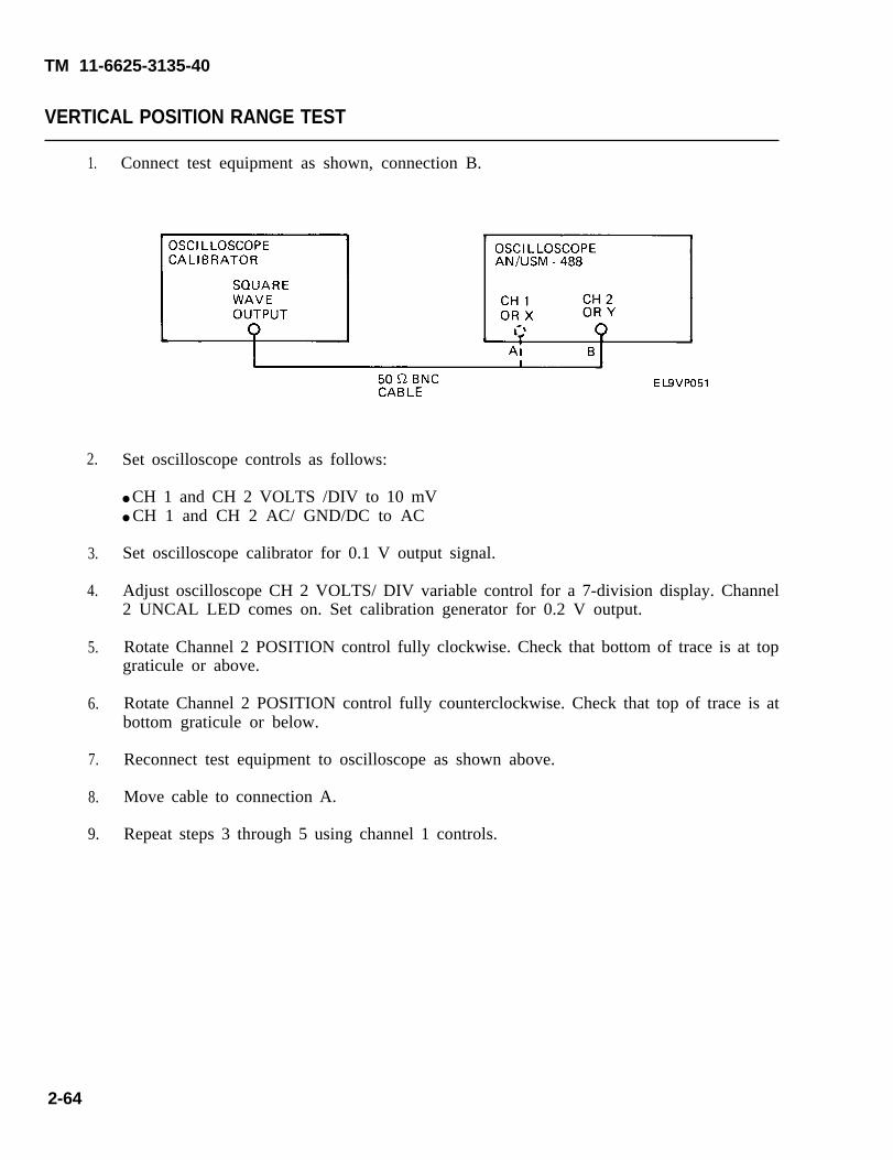
TM 11-6625-3135-40
VERTICAL POSITION RANGE TEST
1. Connect test equipment as shown, connection B.
2.
3.
4.
5.
6.
7.
8.
9.
Set oscilloscope controls as follows:
CH 1 and CH 2 VOLTS /DIV to 10 mV CH 1 and CH 2 AC/ GND/DC to AC
Set oscilloscope calibrator for 0.1 V output signal.
Adjust oscilloscope CH 2 VOLTS/ DIV variable control for a 7-division display. Channel2 UNCAL LED comes on. Set calibration generator for 0.2 V output.
Rotate Channel 2 POSITION control fully clockwise. Check that bottom of trace is at topgraticule or above.
Rotate Channel 2 POSITION control fully counterclockwise. Check that top of trace is atbottom graticule or below.
Reconnect test equipment to oscilloscope as shown above.
Move cable to connection A.
Repeat steps 3 through 5 using channel 1 controls.
2-64

TM 11-6625-3135-40
TRIGGER VIEW GAIN TEST
1. Connect test equipment as shown below, connection A.
2. Set oscilloscope controls as follows:
. Channel 1 and Channel 2 POSITION to midrange. CH 1 and CH 2 VOLTS /DIV to 0.1 V. CH I and CH 2 VOLTS/ DIV variable control to CAL detent
3. Set oscilloscope calibrator for an 0.5 V output.
4. While holding oscilloscope TRIG VIEW switch in, vertically center display with ATRIGGER LEVEL control.
5. Check that display amplitude is 4 to 6 divisions high while holding TRIG VIEW switch in.
6. Move cable to connection B.
7. Set VERTICAL MODE to CH 2.
8. Repeat steps 3 through 5 using channel 2 controls.
9. Connect test equipment as shown below.
2-65

TM 11-6625-3135-40
TRIGGER VIEW GAIN TEST (CONT)
10. Set A SOURCE switch to EXT and repeat steps 3 through 5.
11. Set A EXT COUPLING switch to DC and repeat steps 3 through 5.
12. Set A EXT COUPLING switch to DC÷10, oscilloscope calibrator for a 5 V output, andrepeat steps 3 through 5.
13. Disconnect test equipment.
VERTICAL ABERRATION TEST
1.
2.
3.
4.
5.
6.
7.
2-66
Set oscilloscope controls as follows:
VERTICAL MODE to CH 1BW LIMIT to OffCH 1 and CH 2 VOLTS/DIV to 2 mVCH 1 and CH 2 AC/GND/DC to DCA SOURCE to INTA SEC/ DIV switch to 0.05 us
Connect test equipment as shown below, connection A.
Set oscilloscope calibrator for 1 MHz, 5-division display.
Use vertical POSITION control to set display at center graticule.
Check that display aberrations are within 4% (0.2 division or less).
Repeat step 4 for all VOLTS/DIV switch settings from 5 mV position to 0.2 V position.Adjust calibration generator and attach or remove 10X Attenuator to maintain 5-divisiondisplay at each VOLTS/DIV switch setting.
Set oscilloscope calibrator for minimum output.

TM 11-6625-3135-40
VERTICAL ABERRATION TEST (CONT)
8. Move cable to connection B.
9. Set oscilloscope VERTICAL MODE to CH 2.
10. Set calibration generator for l-MHz, 5 division display.
11. Use vertical POSITION control to set display top at center graticule.
12. Repeat steps 5 and 6 using channel 2 controls.
13. Disconnect test equipment.
VERTICAL BANDWIDTH TEST
1. Set oscilloscope controls as follows:
CH 1 and CH 2 VOLTS/DIV to 2 mV A SEC/DIV to 20 US
2. Connect test equipment as shown below, connection B.
3. Set oscilloscope calibrator for 50 kHz, 6-division display.
2-67
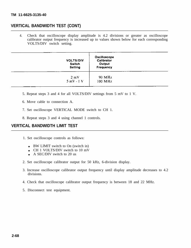
TM 11-6625-3135-40
VERTICAL BANDWIDTH TEST (CONT)
4. Check that oscilloscope display amplitude is 4.2 divisions or greater as oscilloscopecalibrator output frequency is increased up to values shown below for each correspondingVOLTS/DIV switch setting.
5. Repeat steps 3 and 4 for all VOLTS/DIV settings from 5 mV to 1 V.
6. Move cable to connection A.
7. Set oscilloscope VERTICAL MODE switch to CH 1.
8. Repeat steps 3 and 4 using channel 1 controls.
VERTICAL BANDWIDTH LIMIT TEST
1. Set oscilloscope controls as follows:
. BW LIMIT switch to On (switch in). CH 1 VOLTS/DIV switch to 10 mV. A SEC/DIV switch to 20 us
2. Set oscilloscope calibrator output for 50 kHz, 6-division display.
3. Increase oscilloscope calibrator output frequency until display amplitude decreases to 4.2divisions.
4. Check that oscilloscope calibrator output frequency is between 18 and 22 MHz.
5. Disconnect test equipment.
2-68

TM 11-6625-3135-40
VERTICAL COMMON-MODE REJECTION RATlO TEST
1.
2.
3.
4.
5.
6.
7.
8.
9.
10.
11.
12.
13.
Set oscilloscope controls as follows:
. BW LIMIT switch to Off (switch out). CH 2 VOLTS/DIV switch to 10 mV. INVERT switch to On
Connect test equipment as shown below.
Set oscilloscope calibrator for 80 MHz, 6-division display.
Adjust Channel 1 POSITION control to vertically center display.
Set VERTICAL MODE switch to CH 2 and use Channel 2 POSITION control tovertically center display.
Set VERTICAL MODE switches to BOTH and ADD.
Check that display amplitude is 0.6 division or less.
If display amplitude is 0.6 division or less, go to step 17. If display amplitude is more than0.6 division, go to step 9.
Set VERTICAL MODE switch to CH 1.
Set oscilloscope calibrator for 50 kHz, 6-division display.
Set VERTICAL MODE switch to BOTH.
Adjust CH 1 or CH 2 VOLTS/DIV variable control for minimum display amplitude.
Set VERTICAL MODE switch to CH 1.
2-69
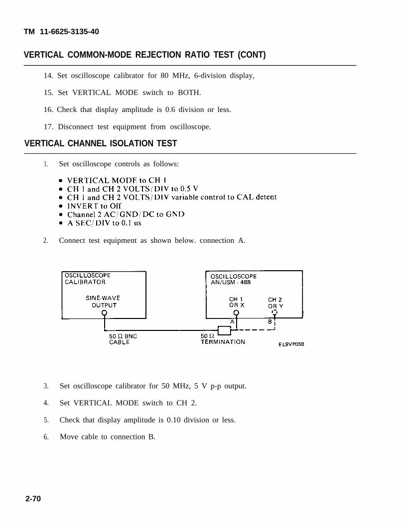
TM 11-6625-3135-40
VERTICAL COMMON-MODE REJECTION RATIO TEST (CONT)
14. Set oscilloscope calibrator for 80 MHz, 6-division display,
15. Set VERTICAL MODE switch to BOTH.
16. Check that display amplitude is 0.6 division or less.
17. Disconnect test equipment from oscilloscope.
VERTICAL CHANNEL ISOLATION TEST
1. Set oscilloscope controls as follows:
2. Connect test equipment as shown below. connection A.
3. Set oscilloscope calibrator for 50 MHz, 5 V p-p output.
4. Set VERTICAL MODE switch to CH 2.
5. Check that display amplitude is 0.10 division or less.
6. Move cable to connection B.
2-70

TM 11-6625-3135-40
VERTICAL CHANNEL ISOLATION TEST (CONT)
7. Set oscilloscope controls as follows:
8. Check that display amplitude is 0.10 division or less.
9. Disconnect test equipment.
END OF TASK
b. Horizontal Circuits Tests. Horizontal circuit tests are structured as one task, and should beperformed in their entirety and in the order presented to ensure correct control settings for each test.
2-71
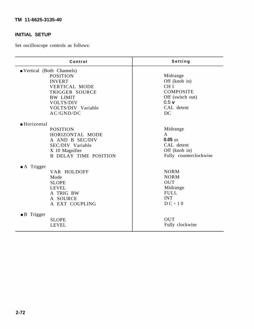
TM 11-6625-3135-40
INITIAL SETUP
Set oscilloscope controls as follows:
Contro l
Vertical (Both Channels)POSITIONINVERTVERTICAL MODETRIGGER SOURCEBW LIMITVOLTS/DIVVOLTS/DIV VariableAC/GND/DC
HorizontalPOSITIONHORIZONTAL MODEA AND B SEC/DIVSEC/DIV VariableX 10 MagnifierB DELAY TIME POSITION
A TriggerVAR HOLDOFFModeSLOPELEVELA TRIG BWA SOURCEA EXT COUPLING
B TriggerSLOPELEVEL
S e t t i n g
MidrangeOff (knob in)CH 1COMPOSITEOff (switch out)0.5 vCAL detentDC
MidrangeA0.05 usCAL detentOff (knob in)Fully counterclockwise
NORMNORMOUTMidrangeFULLINTD C ÷ 1 0
OUTFully clockwise
2-72
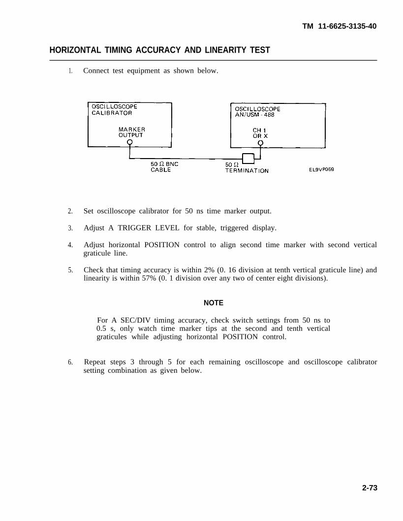
TM 11-6625-3135-40
HORIZONTAL TIMING ACCURACY AND LINEARITY TEST
1. Connect test equipment as shown below.
2. Set oscilloscope calibrator for 50 ns time marker output.
3. Adjust A TRIGGER LEVEL for stable, triggered display.
4. Adjust horizontal POSITION control to align second time marker with second verticalgraticule line.
5. Check that timing accuracy is within 2% (0. 16 division at tenth vertical graticule line) andlinearity is within 57% (0. 1 division over any two of center eight divisions).
NOTE
For A SEC/DIV timing accuracy, check switch settings from 50 ns to0.5 s, only watch time marker tips at the second and tenth verticalgraticules while adjusting horizontal POSITION control.
6. Repeat steps 3 through 5 for each remaining oscilloscope and oscilloscope calibratorsetting combination as given below.
2-73
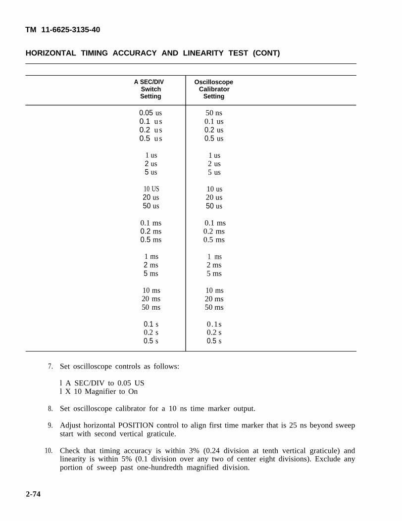
TM 11-6625-3135-40
HORIZONTAL TIMING ACCURACY AND LINEARITY TEST (CONT)
A SEC/DIVSwitchSetting
0.05 us0.1 u s0.2 u s0.5 u s
1 us2 us5 us
10 US20 us50 us
0.1 ms0.2 ms0.5 ms
1 ms2 ms5 ms
10 ms20 ms50 ms
0.1 s0.2 s0.5 s
OscilloscopeCalibrator
Setting
50 ns0.1 us0.2 us0.5 us
1 us2 us5 us
10 us20 us50 us
0.1 ms0.2 ms0.5 ms
1 ms2 ms5 ms
10 ms20 ms50 ms
0.1s0.2 s0.5 s
7.
8.
9.
10.
Set oscilloscope controls as follows:
l A SEC/DIV to 0.05 USl X 10 Magnifier to On
Set oscilloscope calibrator for a 10 ns time marker output.
Adjust horizontal POSITION control to align first time marker that is 25 ns beyond sweepstart with second vertical graticule.
Check that timing accuracy is within 3% (0.24 division at tenth vertical graticule) andlinearity is within 5% (0.1 division over any two of center eight divisions). Exclude anyportion of sweep past one-hundredth magnified division.
2-74

TM 11-6625-3135-40
HORIZONTAL TIMING ACCURACY AND LINEARITY TEST (CONT)
11. Repeat steps 9 and 10 for each remaining A SEC/ DIV and oscilloscope calibrator settingcombination given below.
A SEC/DIVSwitchSetting
0.05 us0.1 us0.2 us0.5 us
1 us2 us5 us
10 us20 us50 us
0.1 ms0.2 ms0.5 ms
1 ms2 ms5 ms
10 ms20 ms50 ms
0.1 s0.2 s0.5 s
12. Set oscilloscope controls as follows:
HORIZONTAL MODE to B A SEC/DIV to 0.1 U S
B SEC/DIV to 0.05 U S
X 10 Magnifier to Off
OscilloscopeCalibrator
Setting
10 ns10 ns20 ns50 ns
0.1 us0.2 us0.5 us
1 us2 us5 us
10 US20 us50 us
0.1 ms0.2 ms0.5 ms
1 ms2 ms5 ms
10 ms20 ms50 ms
13. Repeat steps 2 through 6 using each B SEC/DIV and oscilloscope calibrator settingcombination given below. Keep A SEC/DIV switch at one setting slower than BSEC/ DIV switch for the 0.05 us and 0.1 us steps.
2-75

TM 11-6625-3135-40
HORIZONTAL TIMING ACCURACY AND LINEARITY TEST (CONT)
B SEC/DIVSwitchSetting
0.05 us0.1 us0.2 us0.5 us
1 us2 us5 us
10 us20 us50 us
0.1 ms0.2 ms0.5 ms
1 ms2 ms5 ms
10 ms20 ms50 ms
OscilloscopeCalibrator
Setting
50 ns0.1 us0.2 us0.5 us
1 us2 us5 us
10 us20 us50 us
0.1 ms0.2 ms0.5 ms
1 ms2 ms5 ms
10 ms20 ms50 ms
14.
15.
16.
17.
18.
Set oscilloscope controls as
l B SEC/DIV to 0.05 USl X 10 Magnifier to On
follows:
Set oscilloscope calibrator for 10 ns time marker output.
Adjust horizontal POSITION control to align first time marker that is 25 ns beyond sweepstart with second vertical graticule.
Check that timing accuracy is within 3% (0.24 division at tenth vertical graticule) andlinearity is within 5% (O. 1 division over any two of center eight divisions). Exclude anyportion of sweep past one-hundredth magnified division.
Repeat steps 16 and 17 for each remaining B SEC/DIV and oscilloscope calibrator settingcombination given below.
2-76

TM 11-6625-3135-40
HORIZONTAL TIMING ACCURACY AND LINEARITY TEST (CONT)
B SEC/DIV OscilloscopeSwitch CalibratorSetting Setting
0.05 us0.1 us0.2 us0.5 us
1 us2 us5 us
10 us20 us50 us
0.1 ms0.2 ms0.5 ms
1 ms2 ms5 ms
10 ms20 ms50 ms
10 ns10 ns20 ns50 ns0.1 us0.2 us0.5 us
1 us2 us5 us10 us20 us50 us
0.1 ms0.2 ms0.5 ms
1 ms2 ms5 ms
HORIZONTAL VARIABLE RANGE AND SWEEP SEPARATION TEST
1. Set oscilloscope controls as follows:
HORIZONTAL MODE to A A AND B SEC/DIV to 0.2 ms SEC/ DIV variable control to fully counterclockwise X 10 Magnifier to Off A TRIGGER mode to P-P AUTO
2. Set oscilloscope calibrator for 0.5 ms time marker output.
3. Check that time markers in display are 1 division or less apart.
4. Set oscilloscope controls as follows:
CH 1 AC/GND/DC to GND SEC/DIV variable control to CAL detent HORIZONTAL MODE to ALT
2-77
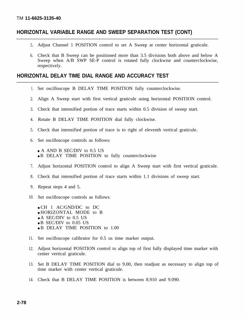
TM 11-6625-3135-40
HORIZONTAL VARIABLE RANGE AND SWEEP SEPARATION TEST (CONT)
5.
6.
Adjust Channel 1 POSITION control to set A Sweep at center horizontal graticule.
Check that B Sweep can be positioned more than 3.5 divisions both above and below ASweep when A/B SWP SE-P control is rotated fully clockwise and counterclockwise,respectively.
HORIZONTAL DELAY TIME DIAL RANGE AND ACCURACY TEST
1.
2.
3.
4.
5.
6.
7.
8.
9.
10.
11.
12.
13.
14.
2-78
Set oscilloscope B DELAY TIME POSITION fully counterclockwise.
Align A Sweep start with first vertical graticule using horizontal POSITION control.
Check that intensified portion of trace starts within 0.5 division of sweep start.
Rotate B DELAY TIME POSITION dial fully clockwise.
Check that intensified portion of trace is to right of eleventh vertical graticule.
Set oscilloscope controls as follows:
A AND B SEC/DIV to 0.5 US B DELAY TIME POSITION to fully counterclockwise
Adjust horizontal POSITION control to align A Sweep start with first vertical graticule.
Check that intensified portion of trace starts within 1.1 divisions of sweep start.
Repeat steps 4 and 5.
Set oscilloscope controls as follows:
CH 1 AC/GND/DC to DC HORIZONTAL MODE to B A SEC/DIV to 0.5 US B SEC/DIV to 0.05 US B DELAY TIME POSITION to 1.00
Set oscilloscope calibrator for 0.5 us time marker output.
Adjust horizontal POSITION control to align top of first fully displayed time marker withcenter vertical graticule.
Set B DELAY TIME POSITION dial to 9.00, then readjust as necessary to align top oftime marker with center vertical graticule.
Check that B DELAY TIME POSITION is between 8.910 and 9.090.

TM 11-6625-3135-40
HORIZONTAL DELAY TIME DIAL RANGE AND ACCURACY TEST (CONT)
15. Repeat steps 12 through 14 for each remaining A AND B SEC/DIV and oscilloscopecalibrator setting combination given below.
A SEC/DIV B SEC/DIV MarkerSwitch Setting Switch Setting Output Setting
0.5 us 0.05 us 0.5 us5 us 0.5 us 5 us
0.5 ms 50 us 0.5 ms5 ms 0.5 ms 5 ms
16.
17.
18.
19.
20.
21.
22.
Set oscilloscope controls as follows:
A SEC/DIV to 0.5 ms B SEC/DIV to 50 US B DELAY TIME POSITION to 1.00
Set oscilloscope calibrator for 0.5 ms time marker output.
Adjust horizontal POSITION control to align time marker rising edge with center verticalgraticule.
Turn B DELAY TIME POSITION dial to position the next time marker leading edge oncenter vertical graticule.
Check that B DELAY TIME POSITION dial setting is 0.980 to 1.020 greater thanprevious setting.
Set B DELAY TIME POSITION dial to the exact integer setting.
Repeat steps 18 through 21 for each successive time marker up to marker corresponding toB DELAY TIME POSITION setting of 10.00.
2-79

TM 11-6625-3135-40
HORIZONTAL DELAY JITTER TEST
1.
2.
3.
4.
Set oscilloscope controls as follows:
A SEC/DIV to 0.5 ms B SEC/DIV to 0.5 US B DELAY TIME POSITION to 10.00
Set oscilloscope calibrator for 50 us time marker output.
Rotate B DELAY TIME POSITION dial counterclockwise to position a time markerwithin graticule area for each major dial division.
Check that time marker leading edge jitter does not exceed 0.5 division. Disregard slowdrift.
HORIZONTAL POSITION RANGE TEST
1.
2.
3.
4.
5.
6.
7.
8.
9.
10.
Set oscilloscope controls as follows:
HORIZONTAL MODE to A A SEC/DIV to 10 US
Set oscilloscope calibrator for 10 us time marker output.
Set horizontal POSITION control fully clockwise. Check that sweep start is to right ofcenter vertical graticule.
Set horizontal POSITION control fully counterclockwise. Check that eleventh timemarker is to left of center vertical graticule.
Set oscilloscope calibrator for 50 us time marker output.
Adjust horizontal POSITION control to align third time marker with center verticalgraticule.
Set X1O Magnifier to On.
Set horizontal POSITION control fully counterclockwise. Check that magnified timemarker is left of center vertical graticule.
Set horizontal POSITION control fully clockwise. Check that sweep start is to right ofcenter vertical graticule.
Disconnect test equipment.
2-80

TM 11-6625-3135-40
HORIZONTAL X GAIN TEST
1. Set oscilloscope controls as follows:
CH 1 VOLTS/DIV to 10 mVHorizontal POSITION to MidrangeA SEC/DIV to X-YX 10 Magnifier to Off
2. Connect test equipment as shown below.
3. Set oscilloscope calibrator for 50 mV output signal.
4. Use Channel 2 POSITION control to vertically center trace.
5. Check that X display is 4.85 to 5.15 horizontal divisions.
6. Disconnect test equipment.
2-81

TM 11-6625-3135-40
HORIZONTAL X BANDWIDTH TEST
1. Connect test equipment as shown below.
2. Set oscilloscope calibrator for 50 kHz, 5-division horizontal display.
3. Increase oscilloscope calibrator output frequency to 2.5 MHz.
4. Check that display is at least 3.5 horizontal divisions.
HORIZONTAL SWEEP LENGTH TEST
1. Set A SEC/DIV to 0.l ms and use horizontal POSITION control to set sweep start at firstvertical graticule.
2. Check that sweep end is to right of eleventh vertical graticule.
3. Disconnect test equipment.
END OF TASK
2-82

TM 11-6625-3135-40
c. Trigger Circuits Tests. Trigger circuit tests are structured as one task, and should beperformed in their entirety and in the order presented to ensure correct control settings for each test.
Initial Setup Internal A and B Triggering Test H F and LF Reject A Triggering Test External Triggering Test External Triggering Ranges Test Single Sweep Operation Test
INITIAL SETUP
Set oscilloscope controls as follows:
Control
Vertical (Both Channels)POSITIONINVERTVERTICAL MODETRIGGER SOURCEBW LIMITVOLTS/DIVVOLTS/DIV VariableAC/GND/DC
HorizontalPOSITIONHORIZONTAL MODEA AND B SEC/DIVSEC/DIV VariableX10 MagnifierB DELAY TIME POSITION
A TriggerVAR HOLDOFFModeSLOPELEVELA TRIG BWA SOURCEA EXT COUPLING
B TriggerSLOPELEVEL
Setting
MidrangeOff (knob in)CH 1COMPOSITEOff (switch out)5 mVCAL detentDC
MidrangeA0.2 usCAL detentOff (knob in)Fully counterclockwise
NORMP-P AUTOOUTMidrangeFULLINTDC
OUTMidrange
2-83
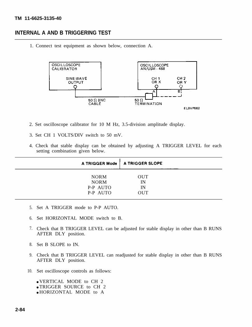
TM 11-6625-3135-40
INTERNAL A AND B TRIGGERING TEST
1. Connect test equipment as shown below, connection A.
2. Set oscilloscope calibrator for 10 M Hz, 3.5-division amplitude display.
3. Set CH 1 VOLTS/DIV switch to 50 mV.
4. Check that stable display can be obtained by adjusting A TRIGGER LEVEL for eachsetting combination given below.
NORM OUTNORM IN
P-P AUTO INP-P AUTO OUT
5.
6.
7.
8.
9.
10.
Set A TRIGGER mode to P-P AUTO.
Set HORIZONTAL MODE switch to B.
Check that B TRIGGER LEVEL can be adjusted for stable display in other than B RUNSAFTER DLY position.
Set B SLOPE to IN.
Check that B TRIGGER LEVEL can readjusted for stable display in other than B RUNSAFTER DLY position.
Set oscilloscope controls as follows:
VERTICAL MODE to CH 2 TRIGGER SOURCE to CH 2 HORIZONTAL MODE to A
2-84

TM 11-6625-3135-40
INTERNAL A AND B TRIGGERING TEST (CONT)
11.
12.
13.
14.
15.
16.
17.
18.
19.
20.
21.
22.
23.
24.
25.
Move cable to connection B.
Repeat steps 3 through 9 using channel 2 controls.
Set oscilloscope controls as follows:
HORIZONTAL MODE to A A SEC/DIV to 0.1 US X 10 Magnifier to On.
Set oscilloscope calibrator for 60 MHz, l-division amplitude display.
Repeat steps 4 through 9 using channel 2 controls.
Set oscilloscope controls as follows:
VERTICAL MODE to CH 1 TRIGGER SOURCE to COMPOSITE HORIZONTAL MODE to A
Move cable to conection A.
Repeat steps 4 through 9 using channel 1 controls.
Set oscilloscope controls as follows:
HORIZONTAL MODE to A A SEC/DIV to 0.05 US
Set oscilloscope calibrator for 100 MHz, 1.5-division display.
Repeat steps 4 through 9 using channel 1 controls.
Set oscilloscope controls as follows:
VERTICAL MODE to CH 2 HORIZONTAL MODE to A
Move cable to connection B.
Repeat steps 4 through 9 using channel 2 controls.
Disconnect test equipment.
2-85

TM 11-6625-3135-40
HF AND LF REJECT A TRIGGERING TEST
1.
2.
3.
4.
5.
6.
7.
8.
9.
10.
11.
12.
Set oscilloscope controls as follows:
VERTICAL MODE to CH 1 HORIZONTAL MODE to A A TRIG BW to HF REJ A SEC/DIV to 0.5 ms X 10 Magnifier to Off (knob in)
Connect test equipment as shown below.
FUNCTION OSCILLOSCOPEGENERATOR AN/USM-488
SI N E-WAVE CH 1OUTPUT OR X
50 Ω BNC 10 XCABLE ATTENUATOR
EL9VP063
Push in and hold TRIG VIEW switch.
Set function generator for 1 kHz, 6-division display.
Increase function generator frequency for a 4.2-division display.
Check that function generator reads between 30 and 50 kHz.
Set A TRIG BW switch to LF REJ.
Push in and hold TRIG VIEW switch.
Set function generator for 500 kHz, 6-division display.
Decrease function generator frequency for 4.2-division display.
Check that function generator reads between 30 and 50 kHz.
Disconnect test equipment.
2-86

TM 11-6625-3135-40
EXTERNAL TRIGGERING TEST
1. Set oscilloscope controls as follows:
VERTICAL MODE to CH 1 HORIZONTAL MODE to A A SOURCE to EXT A SEC/DIV to 0.05 US A TRIG BW to FULL
2. Connect test equipment as shown below.
3.
4.
5.
Set oscilloscope calibrator for 10 MHz, 35 mV output.
Push and hold TRIG VIEW switch.
Check that adjusting A TRIGGER LEVEL produces stable display for each settingcombination given below.
A TRIGGER Mode I A TRIGGER SLOPE
NORM OUTNORM IN
P-P AUTO INP-P AUTO OUT
6.
7.
8.
9.
10.
Set oscillosocpe calibrator for 60 MHz, 120 mV output and X 10 Magnifier to On,
Repeat steps 4 and 5.
Set oscilloscope calibrator for 100 MHz, 150 mV output.
Repeat steps 4 and 5.
Disconnect test equipment.
2-87

TM 11-6625-3135-40
EXTERNAL TRIGGER RANGES TEST
1.
2.
3.
4.
5.
6.
2-88
Set oscilloscope controls as follows:
CH 1 VOLTS/DIV to 0.5 V A SEC/DIV to 20 US X 10 Magnifier to Off A TRIGGER Mode to NORM
Connect test equipment as shown below.
Set oscilloscope calibrator for 50 kHz, 6.4-division display.
Check that display is triggered along entire positive slope throughoutLEVEL range, except not triggered (no trace) for fully clockwise andclockwise.
Set A TRIGGER SLOPE to IN.
Check that display is triggered along entire negative slope throughoutLEVEL range, except not triggered (no trace) for fully clockwise andclockwise.
A TRIGGERfully counter-
A TRIGGERfully counter-
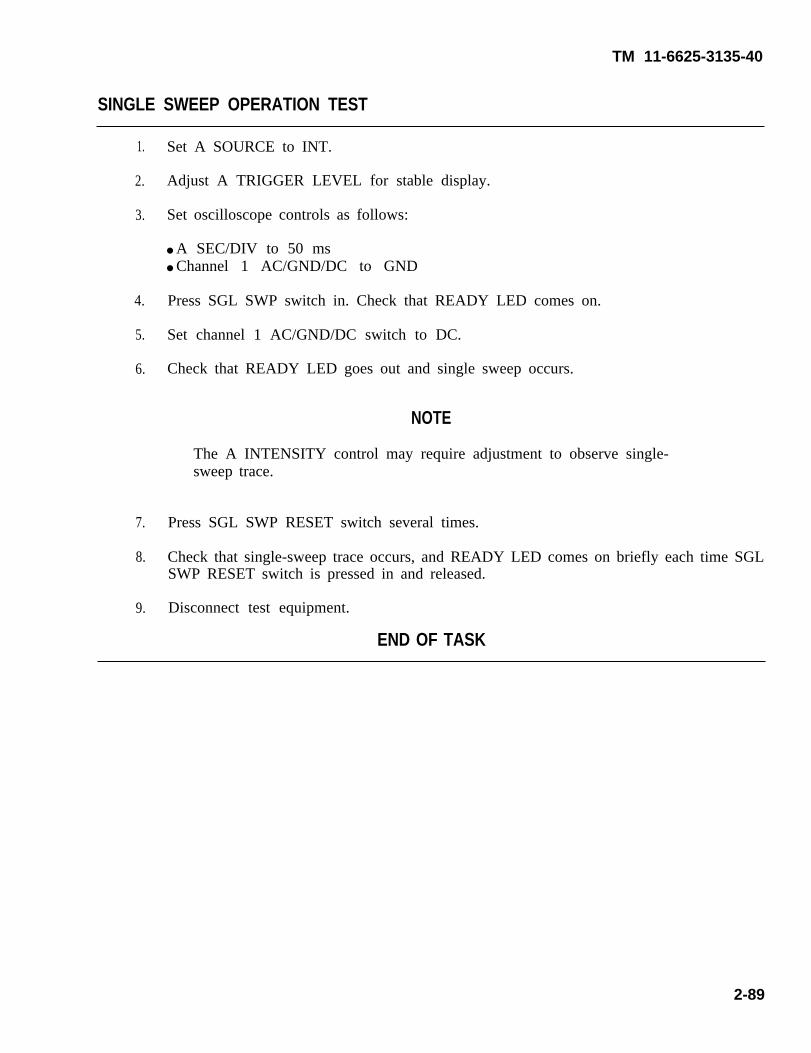
TM 11-6625-3135-40
SINGLE SWEEP OPERATION TEST
1. Set A SOURCE to INT.
2. Adjust A TRIGGER LEVEL for stable display.
3. Set oscilloscope controls as follows:
A SEC/DIV to 50 ms Channel 1 AC/GND/DC to GND
4. Press SGL SWP switch in. Check that READY LED comes on.
5. Set channel 1 AC/GND/DC switch to DC.
6. Check that READY LED goes out and single sweep occurs.
NOTE
The A INTENSITY control may require adjustment to observe single-sweep trace.
7. Press SGL SWP RESET switch several times.
8. Check that single-sweep trace occurs, and READY LED comes on briefly each time SGLSWP RESET switch is pressed in and released.
9. Disconnect test equipment.
END OF TASK
2-89
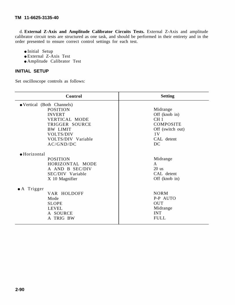
TM 11-6625-3135-40
d. External Z-Axis and Amplitude Calibrator Circuits Tests. External Z-Axis and amplitudecalibrator circuit tests are structured as one task, and should be performed in their entirety and in theorder presented to ensure correct control settings for each test.
Initial Setup External Z-Axis Test Amplitude Calibrator Test
INITIAL SETUP
Set oscilloscope controls as follows:
Control
Vertical (Both Channels)POSITIONINVERTVERTICAL MODETRIGGER SOURCEBW LIMITVOLTS/DIVVOLTS/DIV VariableAC/GND/DC
HorizontalPOSITIONHORIZONTAL MODEA AND B SEC/DIVSEC/DIV VariableX 10 Magnifier
A TriggerVAR HOLDOFFModeSLOPELEVELA SOURCEA TRIG BW
Setting
MidrangeOff (knob in)CH 1COMPOSITEOff (switch out)1VCAL detentDC
MidrangeA20 usCAL detentOff (knob in)
NORMP-P AUTOOUTMidrangeINTFULL
2-90

TM 11-6625-3135-40
EXTERNAL Z-AXIS TEST
1. Connect test equipment as shown below.
2.
3.
4.
5.
Set oscilloscope calibrator for 50 kHz, 5 V output.
Adjust A INTENSITY control as necessary.
Check for noticeable intensity modulation; positive part of sine wave has lower intensitythan negative part.
Disconnect test equipment.
2.91

TM 11-6625-3135-40
AMPLITUDE CALIBRATOR TEST
1.
2.
3.
4.
5.
6.
7.
Set oscilloscope controls as follows:
CH 1 VOLTS/DIV to 10 mV A SEC/DIV to 0.5 ms
Connect X10 probe to oscilloscope as shown below.
Adjust probe compensation for a flat-topped square-wave display.
Check that display amplitude is 4.90 to 5.10 divisions.
Disconnect probe from instrument.
Set POWER switch to OFF.
Remove power cord plug from line source socket.
END OF TASK
2-92

TM 11-6625-3135-40
2-28. ADJUSTMENT PROCEDURE
This section contains adjustment procedures that make sure the oscilloscope meets performancespecifications after replacement of parts. The adjustment procedures are divided into five majorsections, each of which can be performed individually. For example, if only the vertical section hasbeen repaired, it can be adjusted without effect on other sections. After completion of the adjustmentprocedure, do the performance test in para 2-27. The five sections are:
Power Supply and CRT Display Adjustment
Vertical Circuits Adjustments
Horizontal Circuits Adjustments
Trigger Circuits Adjustments
Amplitude Calibrator Adjustment
NOTES
Each section of an adjustment procedure must be done in order and intheir entirety to ensure correct control settings.
All reference designations are on A1 main printed circuit board unlessotherwise noted.
All adjustment points listed in these procedures are located onfig F0-4.
2-93

TM 11-6625-3135-40
INDEX TO ADJUSTMENT PROCEDURE
PagePower Supply and CRT Display Adjustments
Initial Setup . . . . . . . . . . . . . . . . . . . . . . . . . . . . . . . . . . . . . . . . . . . . . . . . . . . . . . . . . . . . . . 2-95Power Supply DC Level Adjustment . . . . . . . . . . . . . . . . . . . . . . . . . . . . . . . . . . . . . . . . . 2-96CRT Grid Bias Adjustment.. . . . . . . . . . . . . . . . . . . . . . . . . . . . . . . . . . . . . . . . . . . . . . . . 2-96Astigmatism Adjustment . . . . . . . . . . . . . . . . . . . . . . . . . . . . . . . . . . . . . . . . . . . . . . . . . . . . 2-96Trace Alignment Adjustment. . . . . . . . . . . . . . . . . . . . . . . . . . . . . . . . . . . . . . . . . . . . . . . . 2-97Geometry Adjustment . . . . . . . . . . . . . . . . . . . . . . . . . . . . . . . . . . . . . . . . . . . . . . . . . . . . . . 2-97
Vertical Circuits AdjustmentsInitial Setup . . . . . . . . . . . . . . . . . . . . . . . . . . . . . . . . . . . . . . . . . . . . . . . . . . . . . . . . . . . . . .Attenuator Step Balance Adjustment . . . . . . . . . . . . . . . . . . . . . . . . . . . . . . . . . . . . . . . . .2/5 mV DC Balance Adjustment . . . . . . . . . . . . . . . . . . . . . . . . . . . . . . . . . . . . . . . . . . . . .Channel l Variable Balance and CH 1 UNCALLED Adjustment. . . . . . . . . . . . . . . . .Channe1 2 Invert Balance and CH 2 UNCALLED Adjustment . . . . . . . . . . . . . . . . . . .MF/LF Compensation and Gain Balance Adjustment . . . . . . . . . . . . . . . . . . . . . . . . . .Vertical Gain Adjustment . . . . . . . . . . . . . . . . . . . . . . . . . . . . . . . . . . . . . . . . . . . . . . . . . . .Attenuator Compensation Adjustment . . . . . . . . . . . . . . . . . . . . . . . . . . . . . . . . . . . . . . . .High-Frequency Compensation, Delay Line Compensation,
and Channel 2 High-Frequency Compensation Adjustment . . . . . . . . . . . . . . . . . . . .2-mV Peaking Compensation Adjustment . . . . . . . . . . . . . . . . . . . . . . . . . . . . . . . . . . . . .
Horizontal Circuits AdjustmentsInitial Setup . . . . . . . . . . . . . . . . . . . . . . . . . . . . . . . . . . . . . . . . . . . . . . . . . . . . . . . . . . . . . .Horizontal Amplifier Gain Adjustment . . . . . . . . . . . . . . . . . . . . . . . . . . . . . . . . . . . . . . .X10 Horizontal Amplifier Gain Adjustment . . . . . . . . . . . . . . . . . . . . . . . . . . . . . . . . . . .Magnifier Registration Adjustment . . . . . . . . . . . . . . . . . . . . . . . . . . . . . . . . . . . . . . . . . . .Delay Dial Timing Adjustment . . . . . . . . . . . . . . . . . . . . . . . . . . . . . . . . . . . . . . . . . . . . . .High-Speed Timing Adjustment . . . . . . . . . . . . . . . . . . . . . . . . . . . . . . . . . . . . . . . . . . . . .5-ns Timing and Linearity Adjustment . . . . . . . . . . . . . . . . . . . . . . . . . . . . . . . . . . . . . . . .X Gain Adjustment . . . . . . . . . . . . . . . . . . . . . . . . . . . . . . . . . . . . . . . . . . . . . . . . . . . . . . . .
2-982-992-992-992-1002-1002-1012-101
2-1032-103
2-1042-1052-1052-1052-1062-1062-1072-107
Trigger Circuits AdjustmentsInitial Setup . . . . . . . . . . . . . . . . . . . . . . . . . . . . . . . . . . . . . . . . . . . . . . . . . . . . . . . . . . . . . . 2-108Trigger Offset Adjustment . . . . . . . . . . . . . . . . . . . . . . . . . . . . . . . . . . . . . . . . . . . . . . . . . . 2-109A Trigger Sensitivity Adjustment . . . . . . . . . . . . . . . . . . . . . . . . . . . . . . . . . . . . . . . . . . . . 2-109P-P Auto Trigger Centering Adjustment . . . . . . . . . . . . . . . . . . . . . . . . . . . . . . . . . . . . . . 2-109B Trigger Sensitivity Adjustment . . . . . . . . . . . . . . . . . . . . . . . . . . . . . . . . . . . . . . . . . . . . . 2-110
External Z-Axis and Amplitude Calibrator AdjustmentInitial Setup . . . . . . . . . . . . . . . . . . . . . . . . . . . . . . . . . . . . . . . . . . . . . . . . . . . . . . . . . . . . . . 2-111External Z-Axis and Amplitude Calibrator Adjustment . . . . . . . . . . . . . . . . . . . . . . . . . 2-111
2-94

TM 11-6625-3135-40
a. Power Supply and CRT Display Adjustments. Perform the power supply and crt displayadjustments in the following order:
Initial Setup Power Supply DC Level Adjustment CRT Grid Bias Adjustment Astigmatism Adjustment Trace Alignment Adjustment Geometry Adjustment
INITIAL SETUP
1.. Plug oscilloscope ac power cord into 115 vac source.
2.. Press POWER ON/ OFF switch to ON and allow at least 20 minutes for oscilloscope towarm up and stabilize before first test.
3. Set oscilloscope controls as follows:
Control
Vertical (Both Channels)POSITIONINVERTVERTICAL MODETRIGGER SOURCEBW LIMITVOLTS/DIVVOLTS/DIV VariableAC/GND/DC
HorizontalPOSITIONHORIZONTAL MODEA AND B SEC/DIVSEC/DIV VariableX 10 Magnifier
A TriggerVAR HOLDOFFModeSLOPELEVELA TRIG BWA SOURCE
Setting
MidrangeOff (knob in)CH 1COMPOSITEOff (switch out)5 mVCAL detentGND
MidrangeAx-YCAL detentOff (knob in)
NORMP-P AUTOOUTMidrangeFULLINT
2-95

TM 11-6625-3135-40
POWER SUPPLY DC LEVEL ADJUSTMENT
1. Connect digital multimeter low lead to chassis ground and connect volts lead to TP961.
2. Check that voltage is -8.6 ±0.04 vdc. If it is, go to step 3. If it is not, adjust R938.
3. Check all other power supply voltages listed below:
Power Supply Test Point Indication
+5.2 vdc Al W968 +5.1 ±0.16 vdc+8.6 vdc A1 W960 +8.6 ±0.17 vdc+30 vdc Al W956 +30 ±0.9 vdc+100 vdc Al W954 +100 ±3.0 vdc
CRT GRID BIAS ADJUSTMENT
1. Connect 50-ohm termination to EXT Z AXIS INPUT connector on the oscilloscope rearpanel,
2. Adjust FOCUS control until well-defined dot is on crt.
3. Rotate A INTENSITY control fully counterclockwise.
4. Adjust R851 for visible dot, then back off until dot just disappears,
5. Disconnect 50-ohm termination.
ASTIGMATISM ADJUSTMENT
1. Set controls to following positions:
A INTENSITY to provide a visible display on crtCH 1 VOLTS/DIV to 5 mVChannel 1 Input Coupling to DCA SEC/DIV to 5 US
2. Connect oscilloscope calibrator sine-wave output to oscilloscope CH 1 OR X inputconnector through 50-ohm cable and 50-ohm termination.
3. Set oscilloscope calibrator for a 50-kHz, 4-division display on oscilloscope crt.
4. Adjust R874 and FOCUS control for best defined waveform.
5. Disconnect termination, cable, and oscilloscope calibrator.
2-96

TM 11-6625-3135-40
TRACE ALIGNMENT ADJUSTMENT
1. Position trace on center horizontal graticule line.
2. Adjust TRACE ROTATION control for optimum alignment of trace with centerhorizontal graticule line.
GEOMETRY ADJUSTMENT
1. Set oscilloscope controls to following positions:
CH 1 VOLTS/DIV to 50 mVA SEC/DIV to 0.1 ms
2. Connect oscilloscope calibrator l-volt, 10-KHZ square-wave signal to oscilloscope CH 1OR X connector through 50-ohm cable.
3. Adjust channel 1 POSITION control to position baseline part of display below the bottomhorizontal graticule line.
4. Adjust SEC/DIV control for 5 markers per division.
5. Adjust R870 for minimum curvature of the time markers at the left and right edges ofgraticule.
6. Turn off and disconnect all equipment.
END OF TASK
b. Vertical Circuits Adjustments. Perform the vertical circuits adjustments in the followingorder:
. Initial Setup. Attenuator Step Balance Adjustment. 2/5 mV DC Balance Adjustment. Channel 1 Variable Balance and CH 1 UNCAL LED Adjustment. Channel 2 Invert Balance and CH 2 UNCAL LED Adjustment. MF/LF Compensation and Gain Balance Adjustment. Vertical Gain Adjustment. Attenuator Compensation Adjustment. High-Frequency Compensation, Delay Line Compensation, and Channel 2 High-FrequencyCompensation Adjustment. 2-mV Peaking Compensation Adjustment
2-97
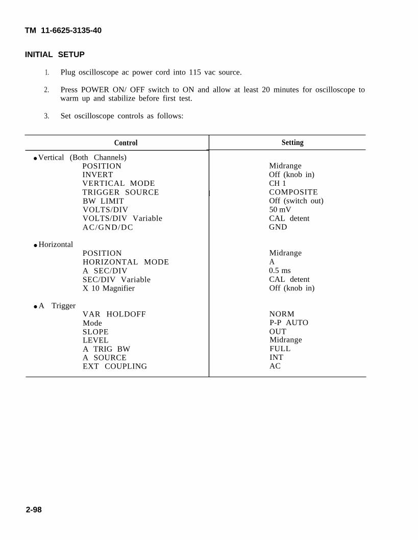
TM 11-6625-3135-40
INITIAL SETUP
1. Plug oscilloscope ac power cord into 115 vac source.
2. Press POWER ON/ OFF switch to ON and allow at least 20 minutes for oscilloscope towarm up and stabilize before first test.
3. Set oscilloscope controls as follows:
Control
Vertical (Both Channels)POSITIONINVERTVERTICAL MODE
Horizontal
A Trigger
Setting
MidrangeOff (knob in)CH 1
TRIGGER SOURCE I COMPOSITEBW LIMITVOLTS/DIVVOLTS/DIV VariableAC/GND/DC
POSITIONHORIZONTAL MODEA SEC/DIVSEC/DIV VariableX 10 Magnifier
VAR HOLDOFFModeSLOPELEVELA TRIG BWA SOURCEEXT COUPLING
Off (switch out)50 mVCAL detentGND
MidrangeA0.5 msCAL detentOff (knob in)
NORMP-P AUTOOUTMidrangeFULLINTAC
2-98

TM 11-6625-3135-40
ATTENUATOR STEP BALANCE ADJUSTMENT
1. Position trace on center horizontal graticule line using channel 1 POSITION control.
2. Set CH 1 VOLTS/DIV switch to 5 mV.
3. Adjust A2R 10 to set trace on center horizontal graticule line.
4. Set CH 1 VOLTS/DIV switch to 50 mV.
5. Set VERTICAL MODE switch to CH 2.
6. Repeat steps 1 through 4 for channnel 2, adjusting A2R60 instead of A2R10.
2/5 MV DC BALANCE ADJUSTMENT
1. Set CH 2 VOLTS/DIV switch to 5 mV.
2. Position trace on center horizontal graticule line using channel 2 POSITION control.
3. Set CH 2 VOLTS/DIV switch to 2 mV.
4. Adjust A2R83 to set trace on center horizontal graticule line.
5. Set VERTICAL MODE switch to CH 1.
6. Repeat steps 1 through 4 for channnel 1, adjusting A2R33 instead of A2R83.
CHANNEL 1 VARIABLE BALANCE AND CH 1 UNCAL LED ADJUSTMENT
1. Set both VOLTS/DIV switches to 10 mV.
2. Rotate CH 1 VOLTS/DIV variable control fully counterclockwise.
3. Check that CH 1 UNCAL LED is on.
4. Position trace on center horizontal graticule line using channel 1 POSITION control.
5. Rotate CH 1 VOLTS/DIV variable control clockwise to CAL detent.
6. Adjust A2R25 to set trace to center horizontal graticule line.
2-99

TM 11-6625-3135-40
CHANNEL 2 INVERT BALANCE AND CH 2 UNCAL LED ADJUSTMENT
1. Set VERTICAL MODE switch to CH 2.
2. Position trace on center horizontal graticule line using channel 2 POSITION control.
NOTE
Once trace is aligned with center horizontal graticule line, do not touchchannel 2 POSITION control when switching INVERT control betweenon and off positions. When pulling INVERT control out (on position),apply pressure around the end of the control. When pushing control in(off position), apply pressure at the end of the control.
3. Set INVERT control to on position (out).
4. Adjust A2R75 to position trace on center graticule line.
5. Set INVERT control to off position (in).
6. Rotate CH 2 VOLTS/DIV variable control fully counterclockwise.
7. Check that CH 2 UNCAL LED is on.
8. Rotate CH 2 VOLTS/DIV variable control clockwise to CAL detent.
MF/LF COMPENSATION AND GAIN BALANCE ADJUSTMENT
1. Set controls to following positions:
INVERT to off (in) positionVERTICAL MODE to CH 2VOLTS/DIV (both) to 10 mVInput Coupling (both) to DCA SEC/DIV to 20 US
2. Connect oscilloscope calibrator high-amplitude square wave output to oscilloscope CH 2OR Y connector through 50-ohm cable, X 10 attenuator, and a 50-ohm termination.
3. Set oscilloscope calibrator output to produce a 10-kHz, 5-division display on oscilloscope.
4. Set top of display on center horizontal graticule line using channel 2 POSITION control.
5. Adjust A2C53 and A2R97 for best front corner and flat top of display.
2-100

TM 11-6625-3135-40
MF/LF COMPENSATION AND GAIN BALANCE ADJUSTMENT (CONT)
6. Move cable to CH 1 or X and set VERTICAL MODE switch to CH 1.
7. Set top of display on center horizontal graticule line using channel 1 POSITION control.
8. Adjust A2C3 and A2R47 for best front corner and flat top of display.
VERTICAL GAIN ADJUSTMENT
1. Connect 50-mv standard-amplitude signal from oscilloscope calibrator to oscilloscope CH1 OR X connector through 50-ohm cable.
2. Set A SEC/DIV switch to 0.2 ms.
3. Adjust R 145 for an exact 5-division display.
4. Move cable to CH 2 or Y and set VERTICAL MODE switch to CH 2.
5. Adjust R 195 for an exact 5-division display.
6. Change oscilloscope calibrator output to IO millivolts and set both oscilloscopeVOLTS/DIV switches to 2 mV.
7. Adjust A2R76 for an exact 5-division display.
8. Move cable to CH 1 or X and set VERTICAL MODE switch to CH 1.
9. Adjust A2R26 for an exact 5-division display.
ATTENUATOR COMPENSATION ADJUSTMENT
1.
2.
3.
4.
5.
6.
Set both input coupling switches to DC and both oscilloscope VOLTS/DIV switches to10 mV.
Connect oscilloscope calibrator high-amplitude square wave output to oscilloscope CH 1OR X connector through a 10X attenuator and a X 10 probe. Ground probe to oscilloscopecalibrator output connector.
Set oscilloscope calibrator output to produce a 1-kHz, 5-division display on oscilloscopeand compensate the probe (TM 11-6625-3 135-12).
Set CH 1 VOLTS/DIV switch to 0.1 V.
Replace probe with a 50-ohm cable.
Set oscilloscope calibrator to produce a 5-division display.
2-101

TM 11-6625-3135-40
ATTENUATOR COMPENSATION ADJUSTMENT (CONT)
7.
8.
9.
10.
11.
12.
13.
14.
15.
16.
17.
18.
19.
NOTE
Use the capacitors listed below, for adjustments in this procedure. Seefig. FO-2 for location of capacitors.
Adjustment Channel 1 Channel 2
10X LF Comp A2C12 A2C6210X Input C A2C11 A2C61100X LF Comp A2C5 A2C55100X Input C A2C4 A2C54
Adjust 10X LF Comp capacitor for best front corner of display.
Replace 50-ohm cable and 10X attenuator with probe.
Set oscilloscope calibrator to produce a 5-division display.
Adjust 10X Input C capacitor for best flat top of display.
Set CH 1 VOLTS/DIV switch to 1 V.
Replace probe with 50-ohm cable.
Set oscilloscope calibrator to produce a 5-division display.
Adjust 100X LF Comp capacitor for best front corner.
Replace 50-ohm cable with probe.
Set oscilloscope calibrator to produce a 5-division display.
Adjust 100X Input C capacitor for best flat top of display.
Set VERTICAL MODE s-witch to CH 2.
Repeat steps 2 through 17 for channel 2.
2-102
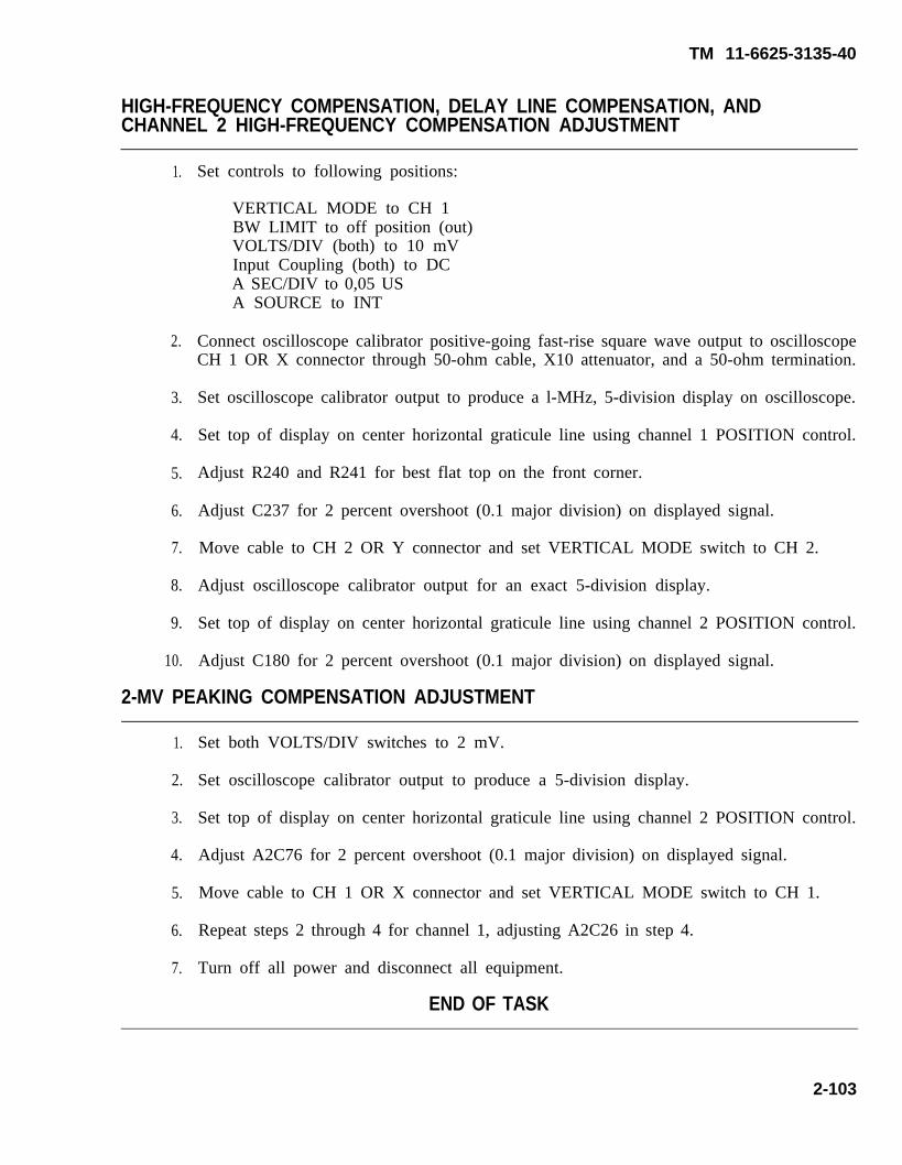
TM 11-6625-3135-40
HIGH-FREQUENCY COMPENSATION, DELAY LINE COMPENSATION, ANDCHANNEL 2 HIGH-FREQUENCY COMPENSATION ADJUSTMENT
1.
2.
3.
4.
5.
6.
7.
8.
9.
10.
Set controls to following positions:
VERTICAL MODE to CH 1BW LIMIT to off position (out)VOLTS/DIV (both) to 10 mVInput Coupling (both) to DCA SEC/DIV to 0,05 USA SOURCE to INT
Connect oscilloscope calibrator positive-going fast-rise square wave output to oscilloscopeCH 1 OR X connector through 50-ohm cable, X10 attenuator, and a 50-ohm termination.
Set oscilloscope calibrator output to produce a l-MHz, 5-division display on oscilloscope.
Set top of display on center horizontal graticule line using channel 1 POSITION control.
Adjust R240 and R241 for best flat top on the front corner.
Adjust C237 for 2 percent overshoot (0.1 major division) on displayed signal.
Move cable to CH 2 OR Y connector and set VERTICAL MODE switch to CH 2.
Adjust oscilloscope calibrator output for an exact 5-division display.
Set top of display on center horizontal graticule line using channel 2 POSITION control.
Adjust C180 for 2 percent overshoot (0.1 major division) on displayed signal.
2-MV PEAKING COMPENSATION ADJUSTMENT
1.
2.
3.
4.
5.
6.
7.
Set both VOLTS/DIV switches to 2 mV.
Set oscilloscope calibrator output to produce a 5-division display.
Set top of display on center horizontal graticule line using channel 2 POSITION control.
Adjust A2C76 for 2 percent overshoot (0.1 major division) on displayed signal.
Move cable to CH 1 OR X connector and set VERTICAL MODE switch to CH 1.
Repeat steps 2 through 4 for channel 1, adjusting A2C26 in step 4.
Turn off all power and disconnect all equipment.
END OF TASK
2-103
TM 11-6625-3135-40
c. Horizontal Circuits Adjustments. Perform the horizontal circuits adjustments in thefollowing order:
Initial Setup. Horizontal Amplifier Gain Adjustment. X 10 Horiontal Amplifier Gain Adjustment. Magnifier Resgistration Adjustment. Delay Dial Time Adjustment. High-Speed Timing Adjustment. 5-ns Timing and Linearity Adjustment. X Gain Adjustment
INITIAL SETUP
1. Plug oscilloscope ac power cord into 115 vac source.
2. Press POWER ON/OFF switch to ON and allow at least 20 minutes for oscilloscope towarm up and stabilize before first test.
3. Set oscilloscope controls as follows:
Control
Vertical (Both Channels)POSITIONINVERTVERTICAL MODETRIGGER SOURCEBW LIMITCH 1 VOLTS/DIVVOLTS/DIV VariableAC/GND/DC
HorizontalPOSITIONHORIZONTAL MODEA SEC/DIVSEC/DIV VariableX10 MagnifierB DELAY TIME POSITION
A TriggerVAR HOLDOFFModeSLOPELEVELA TRIG BWA SOURCE
Setting
MidrangeOff (knob in)CH 1COMPOSITEOff (switch out)0.5 vCAL detentDC
MidrangeA0.1 msCAL detentOff (knob in)Fully Counterclockwise
NORMP-P AUTOOUTMidrangeFULLINT
2-104

TM 11-6625-3135-40
HORIZONTAL AMPLIFIER GAIN ADJUSTMENT
1. Connect oscilloscope calibrator time-mark generator 0.1-ms time markers to oscilloscopeCH 1 OR X connector through 50-ohm cable and 50-ohm termination.
2. Align first time marker with the first (extreme left) vertical graticule line using horizontalPOSITION control.
3. Adjust A4R740 for 1 time marker per division over the center 8 divisions,
NOTE
When making timing measurements, use as a reference the tips of thetime markers positioned at the center horizontal graticule line.
4. Set HORIZONTAL MODE switch to B.
5. Adjust A4R730 for 1 time marker per division.
X1O HORIZONTAL AMPLIFIER GAIN ADJUSTMENT
1. Set controls to following positions:
HORIZONTAL MODE to AX10 Magnifier to on position (out)
2. Select 10-US time markers from the oscilloscope calibrator.
3. Align the nearest time marker to the first vertical graticule line with the horizontalPOSITION control.
4. Adjust A4R754 for 1 time marker per division.
MAGNIFIER REGISTRATION ADJUSTMENT
1. Set A SEC/DIV switch to 0.2 ms.
2. Select 1 ms time markers from the oscilloscope calibrator.
3. Position the middle time marker rising edge to the center vertical graticule line using thehorizontal POSITION control.
4. Set X10 Magnifier to off position (in).
5. Adjust A4R749 to position the middle time marker to the center vertical graticule line.
6. Set X10 Magnifier to on position (out) and check for no horizontal shift in the time marker.
2-105
11-6625-3135-40
DELAY DIAL TIME ADJUSTMENT
1.
2.
3.
4.
5.
6.
7.
Set controls to following positions:
HORIZONTAL MODE to ALTA SEC/DIV to 0.1 msB SEC/DIV to 1 USSEC/DIV variable to CAL detentB DELAY TIME POSITION to 1.00
Select 0.l-ms time markers from the oscilloscope calibrator.
Adjust the A/B SWP SEP control to separate A and B sweeps.
Adjust R646 to that the 2nd A-sweep time marker is intensified and the B-sweep timemarker’s rising edge starts at the beginning of the B sweep.
Set B DELAY TIME POSITION dial to 9.00.
Adjust A5R652 to that the 10th A-sweep time marker is intensified and the B-sweep timemarker’s rising edge starts at the beginning of the B sweep.
Set B DELAY TIME POSITION dial to 1.00.
HIGH-SPEED TIMING ADJUSTMENT
1. Set controls to following positions:
HORIZONTAL MODE to AA SEC/DIV to 1 US
2. Select l-us time markers from the oscilloscope calibrator.
3. Adjust A4C703 for 1 time marker per division over the center 8 divisions.
4. Set HORIZONTAL MODE to B.
5. Adjust A4C713 for 1 time marker per division over the center 8 divisions.
2-106
TM 11-6625-3135-40
5-NS TIMING AND LINEARITY ADJUSTMENT
1. Set controls to following positions:
CH 1 VOLTS/DIV to 0.2 VHORIZONTAL MODE to AA SEC/DIV to 0.05 USX10 Magnifier to on position (out)
2. Select 10-ns time markers from the oscilloscope calibrator.
3. Align the time markers with the vertical graticule lines using the horizontal POSITIONcontrol.
4. Adjust C775 and C785 alternately for one time marker every 2 divisions over the center 8divisions of the magnified sweep.
X GAIN ADJUSTMENT
1. Set controls to following positions:
X10 Magnifier to off position (in)CH 1 VOLTS/DIV to 10 mVA SEC/DIV to X-Y
2. Connect a 50-mV standard-amplitude square-wave signal from the oscilloscope calibratorto the oscilloscope CH 1 OR X input connector through a 50-ohm cable.
3. Adjust R760 for exactly 5-divisions of horizontal deflection.
4. Turn off all power and disconnect all equipment.
END OF TASK
2-107

TM 11-6625-3135-40
d. Trigger Circuits Adjustments. Perform the trigger circuits adjustments in the followingorder:
Initial Setup Trigger Offset Adjustment A Trigger Sensitivity Adjustment P-P Auto Trigger Centering Adjustment B Trigger Sensitivity Adjustment
INITIAL SETUP
1. Plug oscilloscope ac power cord into 115 vac source.
2. Press POWER ON/OFF switch to ON and allow at least 20 minutes for oscilloscope towarm up and stabilize before first test.
3. Set oscilloscope controls as follows:
Control
Vertical (Both Channels)POSITIONINVERTVERTICAL MODETRIGGER SOURCEBW LIMITVOLTS/DIVVOLTS/DIV VariableAC/GND/DC
HorizontalPOSITIONHORIZONTAL MODEA SEC/DIVSEC/DIV VariableX 10 MagnifierB DELAY TIME POSITION
A TriggerVAR HOLDOFFModeSLOPELEVELA TRIG BWA SOURCEA EXT COUPLING
B TriggerSLOPELEVEL
Setting
MidrangeOff (knob in)BOTH-ALTCH 2Off (switch out)0.5 vCAL detentGND
MidrangeA1 msCAL detentOff (knob in)Fully Counterclockwise
NORMP-P AUTOOUTMidrangeFULLINTDC
OUTMidrange
2-108
TM 11-6625-3135-40
TRIGGER OFFSET ADJUSTMENT
1. Set both traces to center horizontal graticule using POSITION controls.
2. Connect digital multimeter low lead to chassis ground and high (volts) lead to A5J9400-1.
3. Check offset voltage reading. It should be less than 100 millivolts. Record reading for usein step 5.
4. Set TRIGGER SOURCE switch to CH 1.
5. Adjust R309 so that voltage reading is the same as in step 3.
A TRIGGER SENSITIVITY ADJUSTMENT
1. Set controls to following positions:
VERTICAL MODE to CH 1CH 1 VOLTS/DIV to 0.1 VInput Coupling (both) to ACA SEC/DIV to 10 US
2. Connect oscilloscope calibrator sine-wave signal through a 50-ohm cable and 50-ohmtermination to the CH 1 OR X input connector.
3. Set oscilloscope calibrator output to produce a 50-kHz, 2.4-division display.
4. Set CH 1 VOLTS/DIV switch to 1 V.
5. Adjust R479 while rotating A TRIGGER LEVEL control slowly, so that A trigger is justable to be maintained.
P-P AUTO TRIGGER CENTERING ADJUSTMENT
1. Set controls to following positions:
CH 1 VOLTS/DIV to 50 mVA TRIGGER SLOPE to outA TRIGGER LEVEL to fully clockwise
2. Set oscilloscope calibrator output to produce a 50-kHz, 5-division display.
3. Set CH 1 VOLTS/DIV switch to 0.5 V.
4. Adjust R434 so that vertical display just solidly triggers on the positive peak of the signal.
2-109
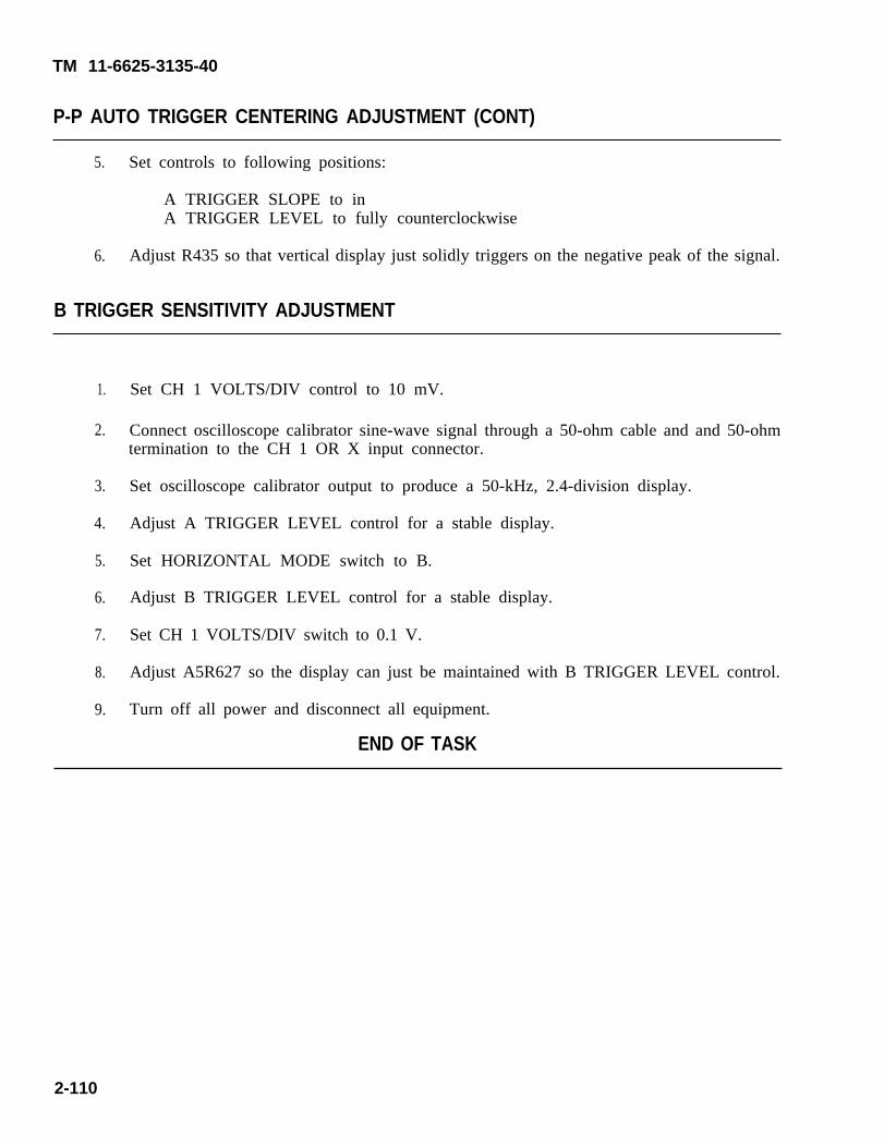
TM 11-6625-3135-40
P-P AUTO TRIGGER CENTERING ADJUSTMENT (CONT)
5. Set controls to following positions:
A TRIGGER SLOPE to inA TRIGGER LEVEL to fully counterclockwise
6. Adjust R435 so that vertical display just solidly triggers on the negative peak of the signal.
B TRIGGER SENSITIVITY ADJUSTMENT
1.
2.
3.
4.
5.
6.
7.
8.
9.
Set CH 1 VOLTS/DIV control to 10 mV.
Connect oscilloscope calibrator sine-wave signal through a 50-ohm cable and and 50-ohmtermination to the CH 1 OR X input connector.
Set oscilloscope calibrator output to produce a 50-kHz, 2.4-division display.
Adjust A TRIGGER LEVEL control for a stable display.
Set HORIZONTAL MODE switch to B.
Adjust B TRIGGER LEVEL control for a stable display.
Set CH 1 VOLTS/DIV switch to 0.1 V.
Adjust A5R627 so the display can just be maintained with B TRIGGER LEVEL control.
Turn off all power and disconnect all equipment.
END OF TASK
2-110

TM 11-6625-3135-40
e. External Z-Axis and Amplitude Calibrator Adjustment.
INITIAL SETUP
1. Plug oscilloscope ac power cord into 115 vac source.
2. Press POWER ON/OFF switch to ON and allow at least 20 minutes for oscilloscope towarm up and stabilize before first test.
3. Set oscilloscope controls as follows:
Control
Vertical (Both Channels)POSITIONVERTICAL MODETRIGGER SOURCEBW LIMITCH 1 VOLTS/DIVCH 1 VOLTS/DIV VariableAC/GND/DC
HorizontalPOSITIONHORIZONTAL MODEA SEC/DIVSEC/DIV VariableX10 Magnifier
A TriggerVAR HOLDOFFModeSLOPELEVELA TRIG BWA SOURCE
Setting
MidrangeCH 1COMPOSITEOff (switch out)10 mVCAL detentAC
MidrangeA0.5 msCAL detentOff (knob in)
NORMP-P AUTOOUTMidrangeFULLINT
EXTERNAL Z-AXIS AND AMPLITUDE CALIBRATOR ADJUSTMENT
Connect 10X probe to CH 1 OR X input connector and insert probe tip in AMP CALoutput jack.
Adjust A3R984 for 5-division display.
Turn off all power and disconnect all equipment.
END OF TASK
2-111

TM 11-6625-3135-40
Section V. PREPARATION FOR STORAGE OR SHIPMENT
2-26. PREPARATION FOR STORAGE OR SHIPMENT
If original packing material was saved, pack oscilloscope in the same manner as it was received. Whenusing packing materials other than the original, use the following guidelines:
a. Wrap oscilloscope in polyethylene sheeting before placing in container.
b. Select corrugated cardboard container having inside dimensions at least 6 inches greater thanoscilloscope dimensions and having a carton test strength of at least 75 pounds.
c. Use plenty of shock-absorbing material all around oscilloscope to protect against damageinsert into a suitable size container.
d. Seal the carton with shipping tape or an industrial stapler.
e. Mark container “FRAGILE-DELICATE INSTRUMENT” to ensure proper handling.
2-27. TYPES OF STORAGE
a. Short-term (administrative) = 1 to 45 days. All equipment in this type must be made readywithin 24 hours for use on a mission. Make sure the next scheduled PMCS is done and all deficienciescorrected before placing in storage. The storage site should provide protection from extreme weatherconditions and allow you to reach it for inspections or exercises if needed.
b. Intermediate = 46 to 180 days.
c. Long-term = over 180 days.
2-112

TM 11-6625-3135-40
APPENDIX AREFERENCES
A-1. SCOPE
This appendix lists all forms, field manuals, technical manuals, and miscellaneous publicationsreferenced in this manual.
A-2. FORMS
Recommended Changes to Publications and Blank Forms . . . . . . . . . . . . . . . DA Form 2028
Recommended Changes to Equipment Technical Manuals . . . . . . . . . . . . . . . DA Form 2028-2
Report of Discrepancy (ROD) . . . . . . . . . . . . . . . . . . . . . . . . . . . . . . . . . . . . . . . . . . . . Form SF 364
Quality Deficiency Report . . . . . . . . . . . . . . . . . . . . . . . . . . . . . . . . . . . . . . . . . . . . . . . . Form SF 368
A-3. TECHNICAL MANUALS
The Army Maintenance Management System (TAMMS) . . . . . . . . . . . . . . . . DA PAM 738-750
Procedures for Destruction of Electronics Material to PreventEnemy Use (Electronics Command) . . . . . . . . . . . . . . . . . . . . . . . . . . . . . . . . . . . . . . . TM 750-244-2
Operator’s and Organization Maintenance Manual,Oscilloscope AN/USM-488 (NSN 6625-01-187-7847) . . . . . . . . . . . . . . . . . . TM 11-6625-3135-12
Organizational, Direct SupportSpecial Tools List, Oscilloscope
A-4. MISCELLANEOUS
and General Support Repair Parts andAN/ US M-488 (NSN 6625-01-187-7847) TM 11-6625-3135-24P
Consolidated Index of Army Publications and Blank Forms . . . . . . . . . . . . . DA Pam 310-1
First Aid for Soldiers . . . . . . . . . . . . . . . . . . . . . . . . . . . . . . . . . . . . . . . . . . . . . . . . . . . . . FM21-11
Safety Precautions for Maintenance of Electrical/ ElectronicEquipment . . . . . . . . . . . . . . . . . . . . . . . . . . . . . . . . . . . . . . . . . . . . . . . . . . . . . . . ... TB 385-4
Abbreviations for Use on Drawings, Specifications, Standardsand in Technical Documents . . . . . . . . . . . . . . . . . . . . . . . . . . . . . . . . . . . . . . . . . . . . . . MI L-STD-12
A-1/(A-2 Blank)


TM 11-6625-3135-12
APPENDIX BEXPENDABLE SUPPLIES AND MATERIALS LIST
Section 1. INTRODUCTION
B-1. SCOPE
This appendix lists expendable supplies and materials you will need to operate and maintain theOscilloscope AN/ USM-488. These items are authorized to you by CTA 50-970, Expendable items(Except Medical, Class V, Repair Parts, and Heraldic Items).
B-2. EXPLANATION OF COLUMNS
a. Column (1) - Item Number. This number is assigned to the entry in the listing and isreferenced in the narrative instructions to identify the material.
b. Column (2) - Level. This column identifies the lowest level of maintenance that requires thelisted item. Enter as applicable:
C-Operator/ CrewO-Organizational MaintenanceF-Direct Support MaintenanceH-General Support Maintenance
c. Column (3) - National Stock Number. This is the National stock number assigned to theitem; use it to request or requisition the item.
d. Column (4) - Description. Indicates the Federal item name and, if required, a description toidentify the item. The last line for each item indicates the Federal Supply Code for Manufacturer(FSCM) (in parentheses) followed by the part number.
e. Column (5) - Unit of Measure (U/M). Indicates the measure used in performing the actualmaintenance function. This measure is expressed by a two-character alphabetical abbreviation (e.g.,ea, in, pr). If the unit of measure differs from the unit of issue, requisition the lowest unit of issue thatwill satisfy your requirements.
B-1

TM 11-6625-3135-40
Section Il. EXPENDABLE SUPPLIES AND MATERIALS
(1)ItemNo.
1
2
3
4
(2)
Level
H
H
H
H
(3)N a t i o n a l
Stock Number
8305-00-267-3015
(4)
Description
Cloth, Cheesecloth, Cotton, LintlessCCC-C-440, Type II, Class 2(8 1348)
Detergent, Liquid, General PurposeSpecification No. P-D-223B
Isopropyl Alcohol
Applicator, Cotton-Tipped
(5)
U/M
yd
oz
oz
ea
B-2

TM 11-6625-3135-40
INDEX
Subject
Paragraph,Figure, Table,
Number
A
AppendicesA— References . . . . . . . . . . . . . . . . . . . . . . . . . . . . . . . . . . . . . . . . . . . . . . . . . . . . . . . . . . . . . . .B—Expendable Supplies and Materials List . . . . . . . . . . . . . . . . . . . . . . . . . . . . . . . . .
Al Main Circuit Board Assembly Replacement . . . . . . . . . . . . . . . . . . . . . . . . . . . . . . . . . .A2 Attenuator Circuit Board Assembly Replacement . . . . . . . . . . . . . . . . . . . . . . . . . . . .A3 Front Panel Circuit Board Assembly Replacement . . . . . . . . . . . . . . . . . . . . . . . . . . .A4 Timing Circuit Board Assembly Replacement, . . . . . . . . . . . . . . . . . . . . . . . . . . . . . . .A5 Alternate Sweep Circuit Board Assembly Replacement . . . . . . . . . . . . . . . . . . . . . .A6 EMI Filter Circuit Board Assembly Replacement . . . . . . . . . . . . . . . . . . . . . . . . . . . .A7 Channe12 Position Pot Circuit Board Assembly Replacement . . . . . . . . . . . . . . .A8 Timing Pot Circuit Board Assembly Replacement. . . . . . . . . . . . . . . . . . . . . . . . . . . .A10 Scale Illumination Circuit Board Assembly Replacement . . . . . . . . . . . . . . . . . . .Abbreviations, List of . . . . . . . . . . . . . . . . . . . . . . . . . . . . . . . . . . . . . . . . . . . . . . . . . . . .Adjustment Procedure . . . . . . . . . . . . . . . . . . . . . . . . . . . . . . . . . . . . . . . . . . . . . . . . . . . . . . . . . . .
B
Bottom Shield Module Removal . . . . . . . . . . . . . . . . . . . . . . . . . . . . . . . . . . . . . . . . . . . . . . . . .
cCabinet Removal . . . . . . . . . . . . . . . . . . . . . . . . . . . . . . . . . . . . . . . . . . . . . . . . . . . . . . . . . . . . . . . . .Checking Unpacking Equipment . . . . . . . . . . . . . . . . . . . . . . . . . . . . . . . . . . . . . . . . . . . . . . . . .Circuit Board Inspection . . . . . . . . . . . . . . . . . . . . . . . . . . . . . . . . . . . . . . . . . . . . . . . . . . . . . . . . .Cleaning . . . . . . . . . . . . . . . . . . . . . . . . . . . . . . . . . . . . . . . . . . . . . . . . . . . . . . . . . . . . . . . . . . . . . . . . . .Common Tools and Equipment . . . . . . . . . . . . . . . . . . . . . . . . . . . . . . . . . . . . . . . . . . . . . . . . . .Consolidated Index of Army Publications and Blank Forms . . . . . . . . . . . . . . . . . . . . .CRT Replacement . . . . . . . . . . . . . . . . . . . . . . . . . . . . . . . . . . . . . . . . . . . . . . . . . . . . . . . . . . . . . . . .
D
Destruction of Army Materials to Prevent Enemy Use . . . . . . . . . . . . . . . . . . . . . . . . . . .Detailed Functional Description . . . . . . . . . . . . . . . . . . . . . . . . . . . . . . . . . . . . . . . . . . . . . . . . .
A-1B-12-252-192-232-202-182-172-242-212-151-112-28
2-22
2-132-52-82-262-11-22-14
1-51-16
Index-1

TM 11-6625-3135-40
Subject
Paragraph,Figure, Table,
Number
E
Equipment DescriptionEquipment Characteristics, Capabilities, and Features. . . . . . . . . . . . . . . . . . . . . . . .Equipment Data . . . . . . . . . . . . . . . . . . . . . . . . . . . . . . . . . . . . . . . . . . . . . . . . . . . . . . . . . . . . . . .Location and Description of Major Internal Components . . . . . . . . . . . . . . . . . . . . .
Expendable Supplies and Materials List . . . . . . . . . . . . . . . . . . . . . . . . . . . . . . . . . . . . . . . . .External Z-Axis and Amplitude Calibrator Adjustment. . . . . . . . . . . . . . . . . . . . . . . . . .External Z-Axis and Amplitude Calibrator Circuits Tests.. . . . . . . . . . . . . . . . . . . . . . .
G
General Functional Description . . . . . . . . . . . . . . . . . . . . . . . . . . . . . . . . . . . . . . . . . . . . . . . . . .General Information
Calibration . . . . . . . . . . . . . . . . . . . . . . . . . . . . . . . . . . . . . . . . . . . . . . . . . . . . . . . . . . . . . . . . . . . . .Consolidated Index of Army Publications and Blank Forms . . . . . . . . . . . . . . . . . .Destruction of Army Material to Prevent Enemy Use . . . . . . . . . . . . . . . . . . . . . . . . .List of Abbreviations . . . . . . . . . . . . . . . . . . . . . . . . . . . . . . . . . . . . . . . . . . . . . . . . . . . . . . . . . .Nomenclature Cross-Reference List . . . . . . . . . . . . . . . . . . . . . . . . . . . . . . . . . . . . . . . . . . . .Preparation for Storage or Shipment . . . . . . . . . . . . . . . . . . . . . . . . . . . . . . . . . . . . . . . . . .Reporting Equipment Improvement Recommendations (EIR) . . . . . . . . . . . . . . . .Safety, Care, and Handling . . . . . . . . . . . . . . . . . . . . . . . . . . . . . . . . . . . . . . . . . . . . . . . . . . . .Scope . . . . . . . . . . . . . . . . . . . . . . . . . . . . . . . . . . . . . . . . . . . . . . . . . . . . . . . . . . . . . . . . . . . . . . . . . .Warranty Information . . . . . . . . . . . . . . . . . . . . . . . . . . . . . . . . . . . . . . . . . . . . . . . . . . . . . . . . .
H
Horizontal Circuits Adjustments . . . . . . . . . . . . . . . . . . . . . . . . . . . . . . . . . . . . . . . . . . . . . . . . .Horizontal Circuits Tests.... . . . . . . . . . . . . . . . . . . . . . . . . . . . . . . . . . . . . . . . . . . . . . . . . . . . . .
L
Location and Description of Major Internal Components . . . . . . . . . . . . . . . . . . . . . . .
M
Maintenance Forms, Records, and Reports . . . . . . . . . . . . . . . . . . . . . . . . . . . . . . . . . . . . . .Maintenance Procedures
AlA2A3A4A5A6A7
Main Circuit Board Assembly Replacement . . . . . . . . . . . . . . . . . . . . . . . . . . . . . . .Attenuator Circuit Board Assembly Replacement. . . . . . . . . . . . . . . . . . . . . . . . . .Front Panel Circuit Board Assembly Replacement . . . . . . . . . . . . . . . . . . . . . . . .Timing Circuit Board Assembly Replacement . . . . . . . . . . . . . . . . . . . . . . . . . . . . . .Alternate Sweep Circuit Board Assembly Replacement. . . . . . . . . . . . . . . . . . . .EMI Filter Circuit Board Assembly Replacement . . . . . . . . . . . . . . . . . . . . . . . . . .Channe12 Position Pot Circuit Board Assembly Replacement . . . . . . . . . . . . .
1-121-141-13B-12-28e2-27d
1-6
1-41-21-51-111-81-61-91-71-11-10
2-28c2-27b
1-13
1-3
2-252-192-232-202-182-172-24
Index-2

TM 11-6625-3135-40
Subject
Paragraph,Figure, Table,
Number
A8 Timing Pot Circuit Board Assembly Replacement . . . . . . . . . . . . . . . . . . . . . . . . .A1O Scale Illumination Circuit Board Assembly Replacement . . . . . . . . . . . . . . . . .Adjustment Procedure . . . . . . . . . . . . . . . . . . . . . . . . . . . . . . . . . . . . . . . . . . . . . . . . . . . . . . . . .
External Z-Axis and Amplitude Calibrator Adjustment . . . . . . . . . . . . . . . . . . . . .Horizontal Circuits Adjustments . . . . . . . . . . . . . . . . . . . . . . . . . . . . . . . . . . . . . . . . . . . .Power Supply and CRT Display Adjustments . . . . . . . . . . . . . . . . . . . . . . . . . . . . . . .Trigger Circuits Adjustments. . . . . . . . . . . . . . . . . . . . . . . . . . . . . . . . . . . . . . . . . . . . . . . .Vertical Circuits Adjustments . . . . . . . . . . . . . . . . . . . . . . . . . . . . . . . . . . . . . . . . . . . . . . .
Bottom Shield Module Removal . . . . . . . . . . . . . . . . . . . . . . . . . . . . . . . . . . . . . . . . . . . . . . .Cabinet Removal . . . . . . . . . . . . . . . . . . . . . . . . . . . . . . . . . . . . . . . . . . . . . . . . . . . . . . . . . . . . . .Cleaning . . . . . . . . . . . . . . . . . . . . . . . . . . . . . . . . . . . . . . . . . . . . . . . . . . . . . . . . . . . . . . . . . . . . . . .CRT Replacement . . . . . . . . . . . . . . . . . . . . . . . . . . . . . . . . . . . . . . . . . . . . . . . . . . . . . . . . . . . . .Performance Tests . . . . . . . . . . . . . . . . . . . . . . . . . . . . . . . . . . . . . . . . . . . . . . . . . . . . . . . . . . . . .
External Z-Axis and Amplitude Calibrator Circuits Tests.. . . . . . . . . . . . . . . . . .Horizontal Circuits Tests.... . . . . . . . . . . . . . . . . . . . . . . . . . . . . . . . . . . . . . . . . . . . . . . . .Trigger Circuits Tests . . . . . . . . . . . . . . . . . . . . . . . . . . . . . . . . . . . . . . . . . . . . . . . . . . . . . . . .Vertical Circuit Tests . . . . . . . . . . . . . . . . . . . . . . . . . . . . . . . . . . . . . . . . . . . . . . . . . . . . . . . .
Power Supply Shield Removal. . . . . . . . . . . . . . . . . . . . . . . . . . . . . . . . . . . . . . . . . . . . . . . . .
N
Nomenclature Cross-Reference List . . . . . . . . . . . . . . . . . . . . . . . . . . . . . . . . . . . . . . . . . . . . . .
0
Oscilloscope AN/ USM-488 . . . . . . . . . . . . . . . . . . . . . . . . . . . . . . . . . . . . . . . . . . . . . . . . . . . . . .Oscilloscope General Block Diagram . . . . . . . . . . . . . . . . . . . . . . . . . . . . . . . . . . . . . . . . . . . . .
2-212-152-282-28e2-28c2-28a2-28d2-28b2-222-132-262-142-272-27d2-27b2-27c2-27a2-16
F 1-0F 1-2
P
Performance Tests . . . . . . . . . . . . . . . . . . . . . . . . . . . . . . . . . . . . . . . . . . . . . . . . . . . . . . . . . . . . . . . . 2-27Power Supply and CRT Display Adjustments . . . . . . . . . . . . . . . . . . . . . . . . . . . . . . . . . . . 2-28aPower Supply Fault Isolation Test . . . . . . . . . . . . . . . . . . . . . . . . . . . . . . . . . . . . . . . . . . . . . . . 2-12Power Supply Shield Removal . . . . . . . . . . . . . . . . . . . . . . . . . . . . . . . . . . . . . . . . . . . . . . . . . . . 2-16Preliminary Servicing and Adjustments of Equipment . . . . . . . . . . . . . . . . . . . . . . . . . . . 2-6Preparation for Storage or Shipment . . . . . . . . . . . . . . . . . . . . . . . . . . . . . . . . . . . . . . . . . . . . 2-26Principles of Operation
Detailed Functional Description . . . . . . . . . . . . . . . . . . . . . . . . . . . . . . . . . . . . . . . . . . . . . . . 1-16General Functional Description . . . . . . . . . . . . . . . . . . . . . . . . . . . . . . . . . . . . . . . . . . . . . . . . 1-15
R
References . . . . . . . . . . . . . . . . . . . . . . . . . . . . . . . . . . . . . . . . . . . . . . . . . . . . . . . . . . . . . . . . . . . . . . . . A-1Repair Parts . . . . . . . . . . . . . . . . . . . . . . . . . . . . . . . . . . . . . . . . . . . . . . . . . . . . . . . . . . . . . . . . . . . . . . 2-3
TM 11-6625-3135-40
Subject
Repair Parts; Special Tools; Test, Measurement, and Diagnostic Equipment(TMDE); and Support Equipment
Common Tools and Equipment . . . . . . . . . . . . . . . . . . . . . . . . . . . . . . . . . . . . . . . . . . . . . . . .Repair Parts . . . . . . . . . . . . . . . . . . . . . . . . . . . . . . . . . . . . . . . . . . . . . . . . . . .Special Tools, TMDE, and Support Equipment . . . . . . . . . . . . . . . . . . . . . . . . . . . . . . .
Reporting Equipment Improvement Recommendations (EAR) . . . . . . . . . . . . . . . . . . .
s
Safety, Care, and Handling . . . . . . . . . . . . . . . . . . . . . . . . . . . . . . . . . . . . . . . . . . . . . . . . . . . . . .Service Upon Receipt
Checking Unpacked Equipment . . . . . . . . . . . . . . . . . . . . . . . . . . . . . . . . . . . . . . . . . . . . . . .Preliminary Servicing and Adjustments of Equipment. . . . . . . . . . . . . . . . . . . . . . . . .Unpacking . . . . . . . . . . . . . . . . . . . . . . . . . . . . . . . . . . . . . . . . . . . . . . . . . . . . . . . . . . .
Special Tools, TMDE, and Support Equipment . . . . . . . . . . . . . . . . . . . . . . . . . . . . . . . . .
T
Trigger Circuits Adjustments. . . . . . . . . . . . . . . . . . . . . . . . . . . . . . . . . . . . . . . . . . . . . . . . . . . . .Trigger Circuits Tests . . . . . . . . . . . . . . . . . . . . . . . . . . . . . . . . . . . . . . . . . . . . . . . . . . .Troubleshooting
Circuit Board Inspection . . . . . . . . . . . . . . . . . . . . . . . . . . . . . . . . . . . . . . . . . . . . . . . . . . . . . . .Introduction . . . . . . . . . . . . . . . . . . . . . . . . . . . . . . . . . . . . . . . . . . . . . . . . . . . . . . . . . . .Power Supply Fault Isolation Test . . . . . . . . . . . . . . . . . . . . . . . . . . . . . . . . . . . . . . . . . . . . .Power Supply Shield Removal. . . . . . . . . . . . . . . . . . . . . . . . . . . . . . . . . . . . . . . . . . . . . . . . .Troubleshooting Procedures. . . . . . . . . . . . . . . . . . . . . . . . . . . . . . . . . . . . . . . . . . . . . . . . . . .Troubleshooting Table . . . . . . . . . . . . . . . . . . . . . . . . . . . . . . . . . . . . . . . . . . . . . . . . . . . . . . . . .Using the Troubleshooting Section . . . . . . . . . . . . . . . . . . . . . . . . . . . . . . . . . . . . . . . . . . . .
u
Unpacking . . . . . . . . . . . . . . . . . . . . . . . . . . . . . . . . . . . . . . . . . . . . . . . . . . . . . . . . . . . . . Using the Troubleshooting Section . . . . . . . . . . . . . . . . . . . . . . . . . . . . . . . . . . . . . . . . . . . . . . .
v
Vertical Circuits Adjustments . . . . . . . . . . . . . . . . . . . . . . . . . . . . . . . . . . . . . . . . . . . . . . . . . . . .Vertical Circuits Tests . . . . . . . . . . . . . . . . . . . . . . . . . . . . . . . . . . . . . . . . . . . . . . . . . . . . . . . . . . . .
w
Warranty Information . . . . . . . . . . . . . . . . . . . . . . . . . . . . . . . . . . . . . . . . . . . . . . . . . . . . . . . . . . . .
Paragraph,Figure, Table,
Number
2-12-32-21-9
1-7
2-52-62-42-2
2-28d2-27c
2-82-72-122-162-112-102-9
2-42-9
2-28b2-27s
1-10
Index-4

TM 11-6625-3135-40
Figure FO-1. Simplified Block Diagram.

TM 11-6625-3135-40
Figure FO-2. A1 Main Board Functional Blocks.

TM 11-6625-3135-40
Figure FO-3. Troubleshooting Test Points(Sheet 1 of 3)

TM 11-6625-3135-40
Figure FO-3. Troubleshooting Test Points(Sheet 2 of 3).

TM 11-6625-3135-40
Figure FO-3. Troubleshooting Test Points(Sheet 3 of 3).

TM 11-6625-3135-40
Figure FO-4. Adjustment Points (Sheet 1 of 2).

TM 11-6625-3135-40
Figure FO-4. Adjustment Points (Sheet 2 of 2)

TM 11-6625-3135-40
Figure FO-5. Channel 1 and Channel 2Attenuators Schematic Diagram.

Figure FO-6. Vertical Preamplifier and OutputAmplifier Schematic Diagram.

TM 11-6625-3135-40
Figure FO-7. Triggering Schematic Diagram.

TM 11-6625-3135-40
Figure FO-8. A Sweep Generator and LogicCircuit Schematic Diagram.

Figure FO-9. Alternate Sweep Logic Circuit
TM 11-6625-3135-40
Schematic Diagram.

Figure FO-10. Amplitude Calibrator and
TM 11-6625-3135-40
Horizontal Output Amplifier Schematic Diagram.

Figure FO-11. Power Supply, Z Axis and Crt
TM 11-6625-3135-40
Circuits Schematic Diagram and Waveforms(Sheet 1 of 2).

Figure FO-11. Power Supply, Z Axis and CrtCircuit Schematic Diagram and Waveforms
(Sheet 2 of 2).
TM 11-6625-3135-40

TM 11-6625-3135-40
Figure FO-12. Power Supply DistributionSchematic Diagram.

TM 11-6625-3135-40
Figure FO-13. Waveform Test Point Locations(Sheet 1 of 2).

TM 11-6625-3135-40
Figure FO-13. Waveform Test Point Locations(Sheet 2 of 2)


PIN: 060574-000

1
* T B 9 - 6 6 2 5 - 2 1 3 9 - 3 5S U P E R S E D E D C O P Y D A T E D 2 6 S E P T E M B E R 1 9 9 0
D E P A R T M E N T O F T H E A R M Y T E C H N I C A L B U L L E T I N
C A L I B R A T I O N P R O C E D U R E F O RO S C I L L O S C O P E A N / U S M - 4 8 8A N D T E K T R O N I X , T Y P E 2 2 3 5
Headquarters, Department of the Army, Washington, DC27 September 1993
Approved for public release; distribution is unlimited.
R E P O R T I N G O F E R R O R S
You can help improve this publicat ion by cal l ing at tent ion to errors and by recommending
improvements and stating your reasons for the recommendations. Your letter or DA Form 2028,
Recommended Changes to Publicat ions, should be mailed direct ly to Director , U.S. Army
TMDE Activity, ATTN: AMXTM-LB-W, Redstone Arsenal, AL 35898-5400. A reply will be.
furnished directly to you.
SECTION I.
II.
III.
P a r a g r a p h
IDENTIFICATION AND DESCRIPTION
Test instrument identification . . . . . . . . . . . . . . . . . . . . . . . . . . . . . . . . . . . . . . . . . . . . . . . . . . . . . . . . . . 1
Forms, records, and reports . . . . . . . . . . . . . . . . . . . . . . . . . . . . . . . . . . . . . . . . . . . . . . . . . . . . . . . . . . . . . 2
Calibration description . . . . . . . . . . . . . . . . . . . . . . . . . . . . . . . . . . . . . . . . . . . . . . . . . . . . . . . . . . . . . . . . . . . . 3
E Q U I P M E N T R E Q U I R E M E N T S
Equipment required . . . . . . . . . . . . . . . . . . . . . . . . . . . . . . . . . . . . . . . . . . . . . . . . . . . . . . . . . . . . . . . . . . . . . . . . . 4
Accessories required . . . . . . . . . . . . . . . . . . . . . . . . . . . . . . . . . . . . . . . . . . . . . . . . . . . . . . . . . . . . . . . . . . . . . . . . 5
CALIBRATION PROCESS
Preliminary i nstruction . . . . . . . . . . . . . . . . . . . . . . . . . . . . . . . . . . . . . . . . . . . . . . . . . . . . . . . . . . . . . . . . . . . 6
Equipment setup . . . . . . . . . . . . . . . . . . . . . . . . . . . . . . . . . . . . . . . . . . . . . . . . . . . . . . . . . . . . . . . . . . . . . . . . . . . . . . 7
Vertical . . . . . . . . . . . . . . . . . . . . . . . . . . . . . . . . . . . . . . . . . . . . . . . . . . . . . . . . . . . . . . . . . . . . . . . . . . . . . . . . . . . . . . . . . . . . 8
Horizontal . . . . . . . . . . . . . . . . . . . . . . . . . . . . . . . . . . . . . . . . . . . . . . . . . . . . . . . . . . . . . . . . . . . . . . . . . . . . . . . . . . . . . . . . 9
Triggering . . . . . . . . . . . . . . . . . . . . . . . . . . . . . . . . . . . . . . . . . . . . . . . . . . . . . . . . . . . . . . . . . . . . . . . . . . . . . . . . . . . . . . . . . 10
Calibrator amplitude . . . . . . . . . . . . . . . . . . . . . . . . . . . . . . . . . . . . . . . . . . . . . . . . . . . . . . . . . . . . . . . . . . . . . . . . 11
Power supply . . . . . . . . . . . . . . . . . . . . . . . . . . . . . . . . . . . . . . . . . . . . . . . . . . . . . . . . . . . . . . . . . . . . . . . . . . . . . . . . . . . 12
Final procedure . . . . . . . . . . . . . . . . . . . . . . . . . . . . . . . . . . . . . . . . . . . . . . . . . . . . . . . . . . . . . . . . . . . . . . . . . . . . . . . . 13
Page
222
33
445
1016202121
*This bulletins supersedes TB 9-6625-2139-35, dated 26 September 1990.
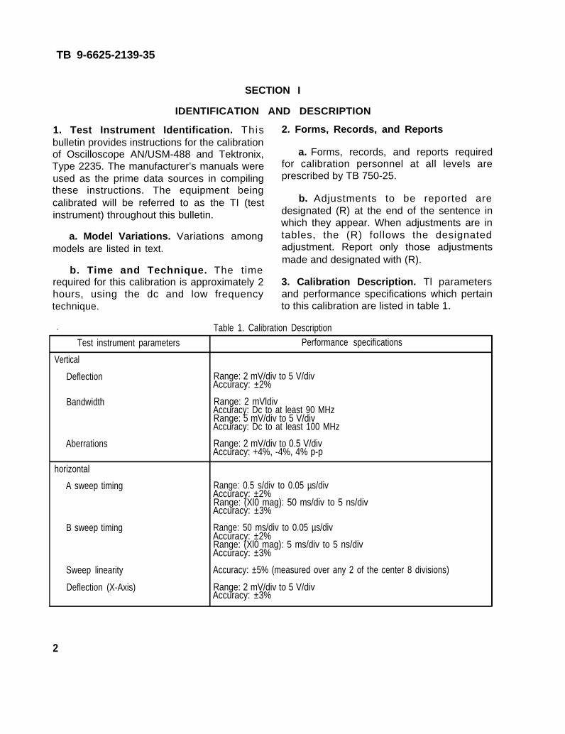
TB 9-6625-2139-35
SECTION I
IDENTIFICATION AND DESCRIPTION
1. Test Instrument Identification. Thisbulletin provides instructions for the calibrationof Oscilloscope AN/USM-488 and Tektronix,Type 2235. The manufacturer’s manuals wereused as the prime data sources in compilingthese instructions. The equipment beingcalibrated will be referred to as the TI (testinstrument) throughout this bulletin.
a. Model Variations. Variations amongmodels are listed in text.
b. Time and Technique. The timerequired for this calibration is approximately 2hours, using the dc and low frequencytechnique.
2. Forms, Records, and Reports
a. Forms, records, and reports requiredfor calibration personnel at all levels areprescribed by TB 750-25.
b. Adjustments to be reported aredesignated (R) at the end of the sentence inwhich they appear. When adjustments are intables, the (R) follows the designatedadjustment. Report only those adjustmentsmade and designated with (R).
3. Calibration Description. Tl parametersand performance specifications which pertainto this calibration are listed in table 1.
. Table 1. Calibration Description
Test instrument parameters Performance specifications
Vertical
Deflection Range: 2 mV/div to 5 V/divAccuracy: ±2%
Bandwidth Range: 2 mVldivAccuracy: Dc to at least 90 MHzRange: 5 mV/div to 5 V/divAccuracy: Dc to at least 100 MHz
Aberrations Range: 2 mV/div to 0.5 V/divAccuracy: +4%, -4%, 4% p-p
horizontal
A sweep timing Range: 0.5 s/div to 0.05 µs/divAccuracy: ±2%Range: (Xl0 mag): 50 ms/div to 5 ns/divAccuracy: ±3%
B sweep timing Range: 50 ms/div to 0.05 µs/divAccuracy: ±2%Range: (Xl0 mag): 5 ms/div to 5 ns/divAccuracy: ±3%
Sweep linearity Accuracy: ±5% (measured over any 2 of the center 8 divisions)
Deflection (X-Axis) Range: 2 mV/div to 5 V/divAccuracy: ±3%
2

TB 9-6625-2139-35
Table 1. Calibration Description - ContinuedTest instrument parameters Performance specifications
A trigger sensitivity Frequency 10 MHz 60 MHz 100 MHz
Internal 0.35 div1 1.0 div 1.5 div
External 35 mV 120 mV 150 mV2
B trigger sensitivity Internal only 0.35 div 1.0 div 1.5 div
Calibrator amplitude Range: 0.5 VAccuracy: ±2%3
!‘0.3 division for type 2235.2200 mV for type 2235.3±5% for type 2235.
SECTION IIEqu ipment Requr iements
4. Equipment Required. Table 2 identifiesthe specific equipment to be used in thiscalibration procedure. This equipment isissued with Secondary Transfer CalibrationStandards Set AN/GSM-286. Alternate itemsmay be used by the calibrating activity. Theitems selected must be verified to performsatisfactorily prior to use and must bearevidence of current calibration. The equipmentmust meet or exceed the minimum usespecifications listed in table 2. The accuracies
listed in table 2 provide a four-to-one ratiobetween the standard and Tl.
5. Accessories Required. The accessoriesrequired for this calibration are common usageaccessories issued as indicated in 4 above,and are not listed in this calibration procedure.The following peculiar accessories are alsorequired for this calibration: Standardizer, 5-80pF, APN 7916146, and Comparator, Tektronix,Type 015-0310-01.
Table 2. Minimun Specifications of Equipment Required
3

TB 9-6625-2139-35
SECTION III
CALIBRATION PROCESS
6. Preliminary Instructions
a. The instructions outlined in paragraphs6 and 7 are preparatory to the calibrationprocess. Personnel should become familiarwith the entire bulletin before beginning thecalibration.
b. Items of equipment used in thisprocedure are referenced within the text bycommon name as listed in table 2.
c. Unless otherwise specified, verify theresult of each test and, whenever the testrequirement is not met, take corrective actionbefore continuing with the calibration.Adjustments required to calibrate the TI areincluded in this procedure. Additionalmaintenance information is contained in themanufacturer’s manual for this TI.
d. When indications specified inparagraphs 8 through 11 are not withintolerance, perform the power supply checkprior to making adjustments. After adjustmentsare made, repeat paragraphs 7 through 11. Donot perform power supply check if all otherparameters are within tolerance.
e. Unless otherwise specified, all controlsand control settings refer to Tl.
7. Equipment Setup
WARNINGHIGH VOLTAGE is used or exposedduring the performance of thiscalibration. DEATH ON CONTACT mayresult if personnel fail to observe safetyprecautions. REDUCE OUTPUT(S) tominimum after each step within theperformance check where applicable.
a. Remove protective cover from TI onlywhen necessary to make adjustments.Replace cover after completing theadjustments.
b. Connect TI to a 115 V ac source.
c. Position controls as listed in (1) through(22) below:
(1) A and B INTENSITY controls fullyccw.
(2) POSITION controls to midrange.(3) CH 2 POSITION INVERT (PULL)
control to in position (AN/USM-488).(4) VERTICAL MODE CH 1 BOTH CH
2 switch to CH 1.(5) VERTICAL MODE TRIGGER
SOURCE CH 1 and CH 2 pushbuttons pressedto COMPOSITE (AN/USM-488).
(6) CH 1 and CH 2 VOLTS/DIV CALcontrols fully cw to detent.
(7) CH 2 INVERT pushbutton to outposition (type 2235).
(8) CH 1 and CH 2 AC GND DCswitches to DC.
(9) BW LIMIT 20 MHz pushbutton toout position.
(10) HORIZONTAL MODE switch to A.(11) A AND B SEC/DIV switches to
.2 ms.(12) X10 CAL control fully cw and in
position.(13) VAR HOLDOFF control fully ccw to
NORM.(14) B TRIGGER SLOPE pushbutton to
OUT:Y .(15) B TRIGGER LEVEL control fully
cw.
4
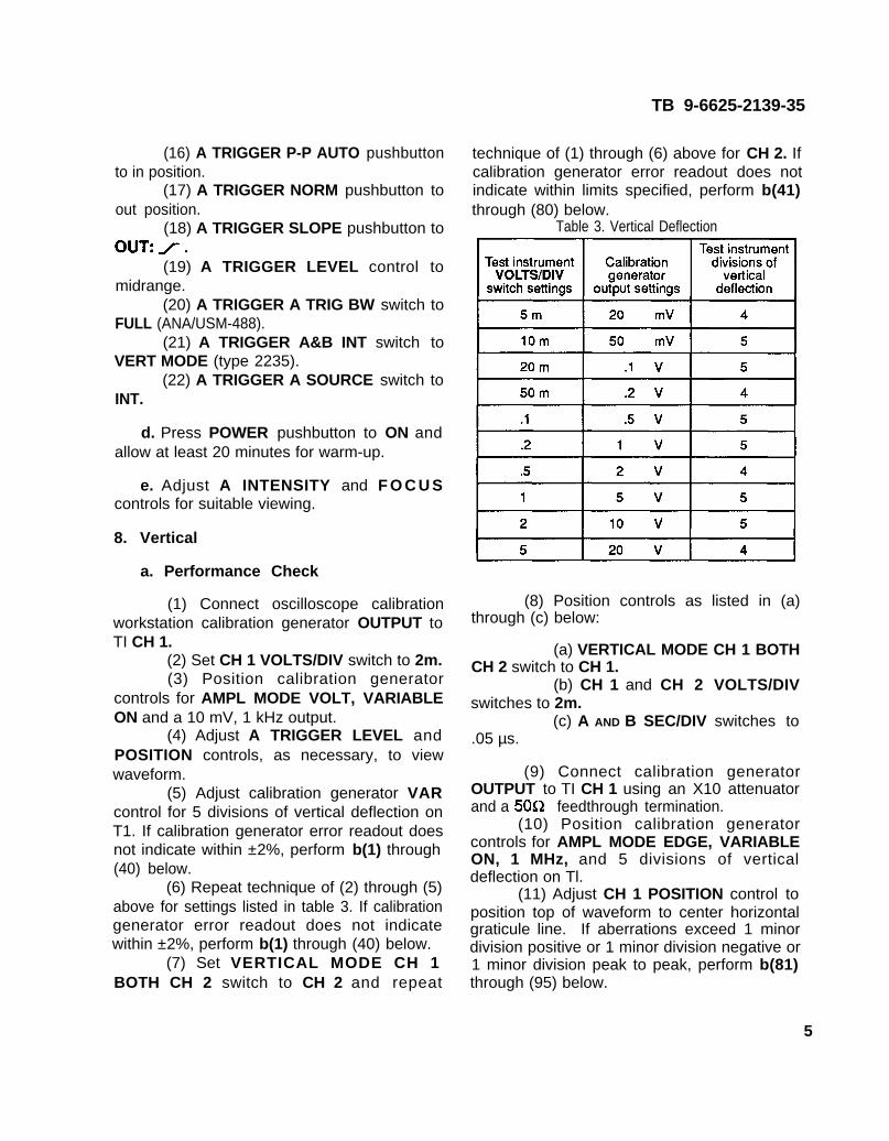
(16) A TRIGGER P-P AUTO pushbuttonto in position.
(17) A TRIGGER NORM pushbutton toout position.
(18) A TRIGGER SLOPE pushbutton to
(19) A TRIGGER LEVEL control tomidrange.
(20) A TRIGGER A TRIG BW switch toFULL (ANA/USM-488).
(21) A TRIGGER A&B INT switch toVERT MODE (type 2235).
(22) A TRIGGER A SOURCE switch toINT.
d. Press POWER pushbutton to ON andallow at least 20 minutes for warm-up.
e. Adjust A INTENSITY and F O C U Scontrols for suitable viewing.
8. Vertical
a. Performance Check
(1) Connect oscilloscope calibrationworkstation calibration generator OUTPUT toTI CH 1.
(2) Set CH 1 VOLTS/DIV switch to 2m.(3) Position calibration generator
controls for AMPL MODE VOLT, VARIABLEON and a 10 mV, 1 kHz output.
(4) Adjust A TRIGGER LEVEL andPOSITION controls, as necessary, to viewwaveform.
(5) Adjust calibration generator VARcontrol for 5 divisions of vertical deflection onT1. If calibration generator error readout doesnot indicate within ±2%, perform b(1) through(40) below.
(6) Repeat technique of (2) through (5)above for settings listed in table 3. If calibrationgenerator error readout does not indicatewithin ±2%, perform b(1) through (40) below.
(7) Set VERTICAL MODE CH 1BOTH CH 2 switch to CH 2 and repeat
TB 9-6625-2139-35
technique of (1) through (6) above for CH 2. Ifcalibration generator error readout does notindicate within limits specified, perform b(41)through (80) below.
Table 3. Vertical Deflection
(8) Position controls as listed in (a)through (c) below:
(a) VERTICAL MODE CH 1 BOTHCH 2 switch to CH 1.
(b) CH 1 and CH 2 VOLTS/DIVswitches to 2m.
(c) A AND B SEC/DIV switches to.05 µs.
(9) Connect calibration generatorOUTPUT to TI CH 1 using an X10 attenuatorand a 50Q feedthrough termination.
(10) Position calibration generatorcontrols for AMPL MODE EDGE, VARIABLEON, 1 MHz, and 5 divisions of verticaldeflection on Tl.
(11) Adjust CH 1 POSITION control toposition top of waveform to center horizontalgraticule line. If aberrations exceed 1 minordivision positive or 1 minor division negative or1 minor division peak to peak, perform b(81)through (95) below.
5

TB 9-6625-2139-35
(12) Repeat technique of (10) and (11) (20) Set VERTICAL MODE CH 1above for CH 1 VOLTS/DIV settings 5 m BOTH CH 2 switch to CH 2 and repeatthrough .2 (remove X10 attenuator at 20m). If technique of (15) through (19) above for CH 2.aberrations exceed 1 minor division positive or1 minor division negative or 1 minor division b. Adjustments.
peak to peak, perform b(81) through (95)below. (1) Disconnect calibration generator
(13) Set VERTICAL MODE CH 1 BOTH CH 2 switch to CH 2 and repeat
(2) Set CH 1 AC GND DC switch to
technique of (9) through (12) above for CH 2. If aberrations are not within limits
(3) Set CH 1 VOLTS/DIV switch to 50m.
specified, perform b(81) through (95) below. (4) Adjust CH 1 POSITION control to(14) Position controls as listed in (a) position trace on center horizontal graticule
through (c) below: line.
O U T P U T from Tl CH 1.
(a) VERTICAL MODE CH 1 BOTHCH 2 switch to CH 1.
(b) CH 1 and CH 2 VOLTS/DIVswitches to 2m.
(c) A AND B SEC/DIV switches to20 µs.
(15) Connect oscilloscope calibrationworkstation leveled sine wave generatorleveling head to TI CH 1 using a feedthrough termination.
(16) Position leveled sine wavegenerator frequency controls for 50 kHz andamplitude controls for 6 divisions of verticaldefection on Tl.
(17) Position leveled sine wave generatorfrequency controls for 4.2 divisions of verticaldeflection on Tl If leveled sine wavegenerator frequency is not 90 MHz or greater,perform b(81 ) through (95) below.
(18) Set CH 1 VOLTS/DIV switch to 5mand repeat technique of (16) and (17) above. Ifleveled sine wave generator frequency is not100 MHz or greater, perform b(81) through(95) below.
(19) Repeat technique of (18) above forCH 1 VOLTS/DIV switch settings 10m through.5. If leveled sine wave generator frequency isnot 100 MHz or greater for each setting,perform b(81) through (95) below.
(5) Set CH 1 VOLTS/DIV switch to 5m.(6) Adjust RIO (fig. 1) to position trace
on center horizontal graticule line.(7) Repeat (3) through (6) above for
minimum trace shift when setting CH 1VOLTS/DIV switch from 50m to 5m.
(8) Adjust CH 1 POSITION control toposition trace on center horizontal graticuleline.
(9) Set CH 1 VOLTS/DIV switch to 2m.(10) Adjust R33 (fig. 1) to position trace
on center horizontal graticule line.(11 ) Set CH 1 VOLTS/DIV switch to 5m.(12) Repeat (8) through (11) above for
minimum trace shift when setting CH 1VOLTS/DIV switch from 5m to 2m.
(13) Connect calibration generatorOUTPUT to TI CH 1 using a feedthroughtermination.
(14) Position controls as listed in (a)through (c) below:
(a) CH 1 VOLTS/DIV switch to10m.
(b) CH 1 AC GND DC switch to DC.(c) A AND B SEC/DIV switches to
20
(15) Position calibration generatorcontrols for AMPL MODE EDGE, VARIABLEON, 10 kHz, and 5 divisions of verticaldeflection on TI.
6
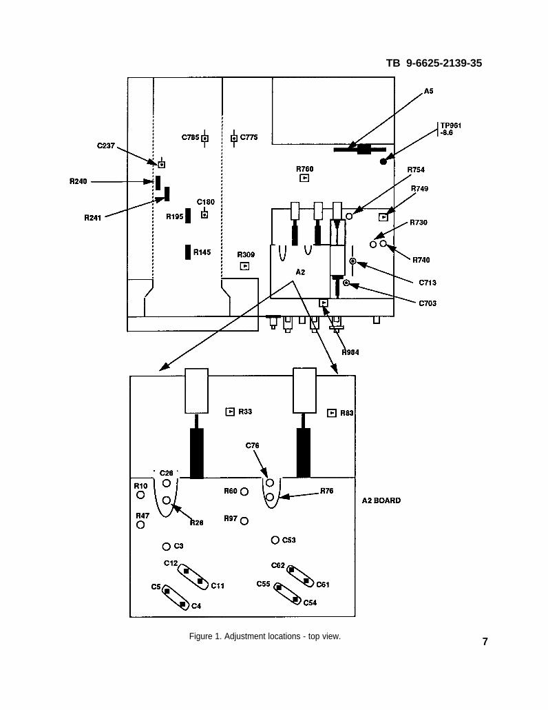
TB 9-6625-2139-35
Figure 1. Adjustment locations - top view. 7

TB 9-6625-2139-35
(16) Adjust CH 1 POSITION control toposition top of waveform to the centerhorizontal graticule line.
(17) Adjust C3 (fig. 1) and R47 (fig. 1)for the best square corner and flat top.
(18) Remove 50Q feedthrough terminationand connect calibration generator OUTPUT toTI CH1.
(19) Position calibration generatorcontrols for AMPL MODE VOLT, VARIABLEON to off, and a 10 mV, 1 kHz output.
(20) Position controls as listed in (a)through (c) below:
(a) CH 1 VOLTS/DIV switch to 2m.(b) A AND B SEC/DIV switches to
.2 ms.(c) CH 1 POSITION control to view
waveform.
(21 ) Adjust R26 (fig. 1) for 5 divisions ofvertical deflection on TI (R).
(22) Set CH 1 VOLTS/DIV switch to10m.
(23) Position calibration generatorcontrols for a 50 mV output.
(24) Adjust R145 (fig. 1) for 5 divisionsof vertical deflection on TI (R).
(25) Connect calibration generatorOUTPUT to TI CH 1 using a 5-80 pFstandardizer.
(26) Position calibration generatorcontrols for AMPL MODE EDGE, VARIABLEON, 1 kHz, and 5 divisions of vertical defectionon Tl.
(27) Adjust 5-80 pF standardizer foroptimum square wave.
(28) Set CH 1 VOLTS/DIV switch to 1.(29) Replace 5-80 pF standardizer with
a 50f2feedthrough termination.(30) Position calibration generator
controls for 5 divisions of vertical deflection onTl.
(31) Adjust C12 (fig. 1) for best frontcorner.
(32) Replace 50Q feedthrough terminationwith a 5-80 pF standardizer and repeat (30)above.
(33) Adjust C11 (fig. 1) for best flat top.(34) Repeat (29) through (33) above
until no further improvement is noted.(35) Set CH 1 VOLTS/DIV switch to 1.(36) Remove 5-80 pF standardizer and
connect calibration generator OUTPUT to TICH 1. Repeat (30) above.
(37) Adjust C5 (fig. 1) for best frontcorner.
(38) Connect calibration generatorOUTPUT to TI CH 1 using a 5-80 pFstandardizer and repeat (30) above.
(39) Adjust C4 (fig. 1) for best flat top.(40) Repeat (36) through (39) above
until no further improvement is noted.(41) Disconnect calibration generator
OUTPUT from TI CH 2.(42) Set CH 2 AC GND DC switch to
AC.(43) Set CH 2 VOLTS/DIV switch to
50m.(44) Adjust CH 2 POSITION control to
position trace on center horizontal graticuleline.
(45) Set CH 2 VOLTS/DIV switch to 5m.(46) Adjust R60 (fig. 1) to position trace
on center horizontal graticule line.(47) Repeat (43) through (46) above for
minimum trace shift when setting CH 2VOLTS/DIV switch from 50m to 5m.
(48) Adjust CH 2 POSITION control toposition trace on center horizontal graticuleline.
(49) Set CH 2 VOLTS/DIV switch to 2m.(50) Adjust R83 (fig. 1) to position trace
on center horizontal graticule line.(51) Set CH 2 VOLTS/DIV switch to 5m.(52) Repeat (48) through (51) above for
minimum trace shift when setting CH 2VOLTS/DIV switch from 5m to 2m.
8
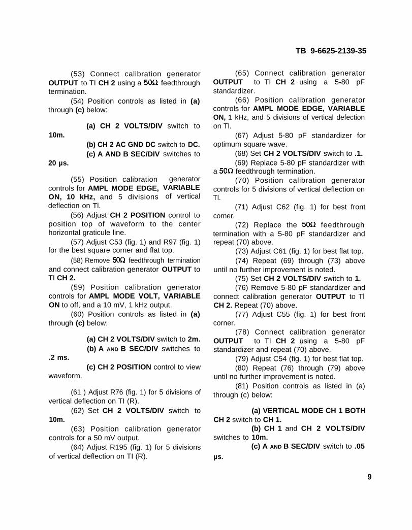
TB 9-6625-2139-35
(53) Connect calibration generatorOUTPUT to TI CH 2 using a 50Q feedthroughtermination.
(54) Position controls as listed in (a)through (c) below:
(a) CH 2 VOLTS/DIV switch to10m.
(b) CH 2 AC GND DC switch to DC.(c) A AND B SEC/DIV
20 µs.
(55) Position calibrationcontrols for AMPL MODE EDGE,ON, 10 kHz, and 5 divisionsdeflection on Tl.
switches to
generatorVARIABLEof vertical
(56) Adjust CH 2 POSITION control toposition top of waveform to the centerhorizontal graticule line.
(57) Adjust C53 (fig. 1) and R97 (fig. 1)for the best square corner and flat top.
(58) Remove 50Q feedthrough terminationand connect calibration generator OUTPUT toTI CH 2.
(59) Position calibration generatorcontrols for AMPL MODE VOLT, VARIABLEON to off, and a 10 mV, 1 kHz output.
(60) Position controls as listed in (a)through (c) below:
(a) CH 2 VOLTS/DIV switch to 2m.(b) A AND B SEC/DIV switches to
.2 ms.(c) CH 2 POSITION control to view
waveform.
(61 ) Adjust R76 (fig. 1) for 5 divisions ofvertical deflection on TI (R).
(62) Set CH 2 VOLTS/DIV switch to10m.
(63) Position calibration generatorcontrols for a 50 mV output.
(64) Adjust R195 (fig. 1) for 5 divisionsof vertical deflection on TI (R).
(65) Connect calibration generatorOUTPUT to TI CH 2 using a 5-80 pFstandardizer.
(66) Position calibration generatorcontrols for AMPL MODE EDGE, VARIABLEON, 1 kHz, and 5 divisions of vertical defectionon Tl.
(67) Adjust 5-80 pF standardizer foroptimum square wave.
(68) Set CH 2 VOLTS/DIV switch to .1.(69) Replace 5-80 pF standardizer with
a 50Q feedthrough termination.(70) Position calibration generator
controls for 5 divisions of vertical deflection onTl.
(71) Adjust C62 (fig. 1) for best frontcorner.
(72) Replace the 50!2 feedthroughtermination with a 5-80 pF standardizer andrepeat (70) above.
(73) Adjust C61 (fig. 1) for best flat top.(74) Repeat (69) through (73) above
until no further improvement is noted.(75) Set CH 2 VOLTS/DIV switch to 1.(76) Remove 5-80 pF standardizer and
connect calibration generator OUTPUT to TlCH 2. Repeat (70) above.
(77) Adjust C55 (fig. 1) for best frontcorner.
(78) Connect calibration generatorOUTPUT to TI CH 2 using a 5-80 pFstandardizer and repeat (70) above.
(79) Adjust C54 (fig. 1) for best flat top.(80) Repeat (76) through (79) above
until no further improvement is noted.(81) Position controls as listed in (a)
through (c) below:
(a) VERTICAL MODE CH 1 BOTHCH 2 switch to CH 1.
(b) CH 1 and CH 2 VOLTS/DIVswitches to 10m.
(c) A AND B SEC/DIV switch to .05µs.
9

TB 9-6625-2139-35
(82) Connect calibration generatorOUTPUT to TI CH 1 using a X10 attenuatorand a 50Q feedthrough termination.
(83) Position calibration generatorcontrols for AMPL MODE EDGE, VARIABLEON, 1 MHz, and 5 divisions of verticaldeflection on Tl.
(84) Adjust CH 1 POSITION control toposition top of waveform to center horizontalgraticule line.
(85) Adjust C237 (fig. 1) for minimumovershoot and R240 (fig. 1) and R241 (fig. 1)for best flat top on front corner of waveform (R).
(86) Set CH 1 VOLTS/DIV switch to 2m.
(87) Position calibration generator controlsfor 5 divisions of vertical deflection on Tl.
(88) Adjust CH 1 POSITION control toposition top of waveform to center horizontalgraticule line.
(89) Adjust C26 (fig. 1) for minimumovershoot on waveform (R).
(90) Set VERTICAL MODE CH 1BOTH CH 2 switch to CH 2 and repeattechnique of (82) through (84) above for CH 2.
(91) Adjust C180 (fig. 1) for minimumovershoot on displayed waveform (R).
(92) Set CH 2 VOLTS/DIV switch to 2m.
(93) Position calibration generator controlsfor 5 divisions of vertical deflection on Tl.
(94) Adjust CH 2 POSITION control toposition top of waveform to center horizontalgraticule line.
(95) Adjust C76 (fig. 1) for minimumovershoot on waveform (R).
9. Horizontal
a. Performance Check
(1) Position controls as listed in (a)through (f) below:
(a) VERTICAL MODE CH 1 BOTHCH 2 switch to CH 1.
(b) CH 1 VOLTS/DIV switch to .5.
(c) A AND B SEC/DIV switches to.05 µs.
(d) B DELAY TIME POSITIONcontrol fully CCW.
(e) B TRIGGER LEVEL controlfully cw.
(f) A TRIGGER NORM pushbuttonpressed.
(2) Connect calibration generatorOUTPUT to TI CH 1 using a 50Q feedthroughtermination.
(3) Position calibration generatorcontrols for MARKERS, VARIABLE ON, and50 nS/D output.
(4) Adjust A TRIGGER LEVEL, AINTENSITY, and CH 1 POSITION controls forsuitable viewing.
(5) Adjust horizontal POSITION control toaline 2d time marker with 2d vertical graticuleline.
(6) Adjust calibration generator VARcontrol to aline 10th time marker with 10thvertical graticule line. If calibration generatorerror readout indication is not within ±2% andlinearity is not within 0.1 division over any 2 ofthe center 8 divisions, perform b(1) through(28) below.
(7) Repeat technique of (3) through (6)for settings listed in table 4. If calibrationgenerator error readout indication is not within±2% and linearity is not within 0.1 division overany 2 of the centerthrough (28) below.
8 divisions, perform b(1)
10
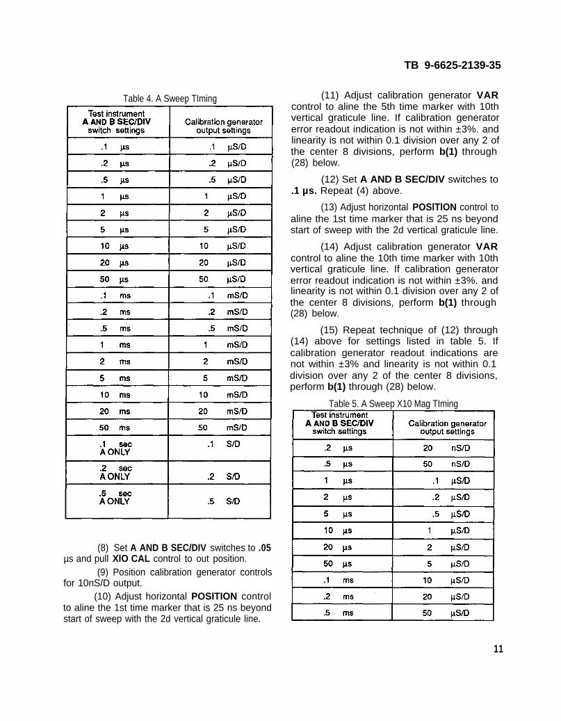
TB 9-6625-2139-35
Table 4. A Sweep TIming (11) Adjust calibration generator VARcontrol to aline the 5th time marker with 10thvertical graticule line. If calibration generatorerror readout indication is not within ±3%. andlinearity is not within 0.1 division over any 2 ofthe center 8 divisions, perform b(1) through(28) below.
(12) Set A AND B SEC/DIV switches to.1 µs. Repeat (4) above.
(13) Adjust horizontal POSlTlON control toaline the 1st time marker that is 25 ns beyondstart of sweep with the 2d vertical graticule line.
(14) Adjust calibration generator VARcontrol to aline the 10th time marker with 10thvertical graticule line. If calibration generatorerror readout indication is not within ±3%. andlinearity is not within 0.1 division over any 2 ofthe center 8 divisions, perform b(1) through(28) below.
(15) Repeat technique of (12) through(14) above for settings listed in table 5. Ifcalibration generator readout indications arenot within ±3% and linearity is not within 0.1division over any 2 of the center 8 divisions,perform b(1) through (28) below.
Table 5. A Sweep X10 Mag TIming
(8) Set A AND B SEC/DIV switches to .05µs and pull XlO CAL control to out position.
(9) Position calibration generator controlsfor 10nS/D output.
(10) Adjust horizontal POSITION controlto aline the 1st time marker that is 25 ns beyondstart of sweep with the 2d vertical graticule line.
11

Table 6.
Table 5.
TB 9-6625-2139-35
(16) Position controls as listed in (a)through (d) below:
(a) HORIZONTAL MODE switch toB.
(b) A SEC/DIV switch to .1 µs.(c) B SEC/DIV switch to .05 µs.(d) X10 CAL control to in position.
(17) Position calibration generatorcontrols for 50 nS/D output.
(18) Adjust A and B TRIGGER LEVEL,B INTENSITY, and CH 1 POSITION controlsfor suitable viewing.
(19) Adjust horizontal POSITION controlto aline 2d time marker with 2d vertical graticuleline.
(20) Adjust calibration generator VARcontrol to aline 10th time marker with 10thvertical graticule line. If calibration generatorerror readout indication is not within ±2% andlinearity is not within 0.1 division over any 2 ofthe center 8 divisions, perform b(1) through(28) below.
(21 ) Repeat technique of (16) through(20) for settings listed in table 6. If calibrationgenerator error readout indication is not within±2% and linearity is not within 0.1 division overany 2 of the center 8 divisions, perform b(1)through (28) below.
(22) Position controls as listed in (a)through (c) below:
(a) A SEC/DIV switch to .1 µs.(b) B SEC/DIV switch to .05 µs.(c) Xl O CAL control to out position.
12

TB 9-6625-2139-35
(23) Position calibration generator controlsfor 10 nS/D output.
(24) Adjust A and B TRIGGER LEVEL,B INTENSITY, and CH 1 POSITION controlsfor suitable viewing.
(25) Adjust horizontal POSIT IONcontrol to aline the 1st time marker that is 25 nsbeyond start of sweep with the 2d verticalgraticule line.
(26) Adjust calibration generator VARcontrol to aline the 5th time marker with 10thvertical graticule line. If calibration generatorerror readout indication is not within ±3% andlinearity is not within 0.1 division over any 2 ofthe center 8 divisions, perform b(1) through(28) below.
(27) Set A SEC/DIV switch to .2µs andB SEC/DIV switch to .1µs. Repeat (24) above.
(28) Adjust horizontal POSITlON control toaline the first time marker that is 25 ns beyondstart of sweep with the 2d vertical graticule- line.
(29) Adjust calibration generator VARcontrol to aline the 10th time marker with 10thvertical graticule line. If calibration generatorerror readout indication is not within ±3% andlinearity is not within 0.1 division over any 2 ofthe center 8 divisions, perform b(l) through(28) below.
(30) Repeat technique of (27) through(29) above for settings listed in table 7. Ifcalibration generator readout indications arenot within ±3% and linearity is not within 0.1division over any 2 of the center 8 divisions,perform b(1) through (28) below.
Table 7. B Sweep X10O Mag Timing
Table 7. B Sweep X1O Mag Timing - Continued
(31 ) Position controls as listed in (a)through (f) below:
(a) A SEC/DIV switch to .5µs.(b) B SEC/DIV switch to .05 µs.(c) Xl0 CAL control to in position.(d) B DELAY TIME POSITION
dial to 1.00.(e) B TRIGGER LEVEL control
fully cw.( f ) A TRIGGER P-P AUTO
pushbutton pressed.(32) Position calibration generator controls
for .5 µS/D output and VARIABLE ON to off.(33) Adjust A TRIGGER LEVEL, B
INTENSITY, and CH 1 POSITION controls forsuitable viewing.
(34) Adjust horizontal POSITION control toaline the first fully displayed time marker withthe center vertical graticule line.
13

TB 9-6625-2139-35
(35) Adjust B DELAY TIME POSITIONdial to approximately 9.00 to aline time markerwith the center vertical graticule line. If BDELAY TIME POSITION dial indication is notbetween 8.91 and 9.09, perform b(29) through(37) below.
(36) Repeat technique of (31) through(35) above for settings listed in table 8. If BDELAY TIME POSITION dial indication is notbetween 8.91 and 9.09 at each setting, performb(29) through (37) below.
Table 8. B Delay Time Position Accuracy
Test instrumentCalibration
A SEC/DIV B SEC/DIV generatorswitch settings switch settings output settings
5 µs .5 µs 5 µS/D
.5 ms 50 µs .5 mS/D
5 m s .5 ms 5 mS/D
.5 s 50 ms1 .5 S/`D1Press A TRIGGER NORM pushbutton.
(37) Remove 50Q feedthrough terminationand connect calibration generator OUTPUT toTI CH1.
(38) Position controls as listed in (a)through (d) below:
(a) CH1 VOLTS/DIV switch to 10 m.(b) HORIZONTAL MODE switch
to A.(c) A AND B SEC/DIV switches to
X-Y.(d) A TRIGGER P-P AUTO
pushbutton pressed.
(39) Position calibration generatorcontrols for AMPL MODE VOLT, VARIABLEON, and a 50 mV, 1 kHz output.
(40) Adjust A INTENSITY and CH 2 andhorizontal POSITION controls for suitableviewing.
14
(41 ) Adjust calibration generator VARcontrol for 5 divisions of horizontal display. Ifcalibration generator error readout indication isnot within ±3%, perform b(38) and (39) below.
b. Adjustments.
(1) Position controls as listed in (a)through (c) below:
(a) HORIZONTAL MODE switchto A.
(b) A AND B SEC/DIV switches to.1 ms.
(c) Xl0 CAL control to in position.
(2) Position calibration generatorcontrols for .1 mS/D output and VARIABLEON to off.
(3) Adjust horizontal POSITION controlto aline 1st time marker with the 1st (extremeleft) vertical graticule line.
(4) Adjust R740 (fig. 1) for 1 timemarker per division over the center 8 divisions(R).
(5) Set HORIZONTAL MODE switchto B and adjust B INTENSITY control forsuitable viewing. Adjust horizontal POSITIONcontrol to aline 1st time marker with 1st verticalgratical line.
(6) Adjust R730 (fig. 1) for 1 timemarker per division over the center 8 divisions(R).
(7) Set HORIZONTAL MODE switchto A and pull Xl0 CAL control to out position.
(8) Position calibration generatorcontrols for 10 µS/D output.
(9) Adjust horizontal POSITION controlto aline the nearest time marker to the 1stvertical graticule line with the 1st verticalgraticule line.
(10) Adjust R754 (fig. 1) for 1 timemarker per division (R).
(11) Set A AND B SEC/DIV switches to.2 ms.

TB 9-6625-2139-35
(12) Position calibration generatorcontrols for 1 mS/D output.
(13) Adjust horizontal POSlTlON controlto position middle time marker to center verticalgraticule line.
(14) Push X10 CAL control to inposition.
(15) Adjust R749 (fig. 1) to position themiddle time marker to the center verticalgraticule line.
(16) Pull X10 CAL control to outposition and check for no horizontal shift intime marker.
(17) Repeat (13) through (16) aboveuntil no further improvement is noted.
(18) Set A AND B SEC/DIV switches to.1 µs and push X10 CAL control to in position.
(19) Position calibration generator controlsfor .1 µS/D output.
(20) Adjust A TRIGGER LEVEL control fora triggered display and horizontal POSlTlONcontrol to aline 1st time marker with 1st verticalgraticule line.
(21) Adjust C703 (fig. 1) for 1 timemarker per division over the center 8 divisions(R).
(22) Position controls as listed in (a)through (c) below:
(a) HORIZONTAL MODE switchto B.
(b) A SEC/DIV switch to 1 µs.(c) B SEC/DIV switch to .1 µs.
(23) Adjust horizontal POSITION controlto aline 1st time marker with 1st verticalgraticule line.
(24) Adjust C713 (fig. 1) for 1 time markerper division over the center 8 divisions (R).
(25) Position controls as listed in (a)through (c) below:
(a) HORIZONTAL MODE switchto A.
(b) A AND B SEC/DIV switches to.05 µs.
(c) X10 CAL control to outposition.
(26) Position calibration generatorcontrols for 10 nS/D output.
(27) Adjust horizontal POSIT IONcontrol to aline the 1st time marker that is 25 nsbeyond start of sweep with the 2d verticalgraticule line.
(28) Adjust C775 (fig. 1) and C785(fig. 1) alternately for 1 time marker every 2divisions over the center 8 divisions (R).
(29) Position controls as listed in (a)through (d) below:
(a) HORIZONTAL MODE switchto ALT.
(b) A SEC/DIV switch to .1 ms.(c) B SEC/DIV switch to 1 µs.(d) B DELAY TIME POSITION
dial to 1.00.
(30) Position calibration generatorcontrols for .1 mS/D output.
(31 ) Adjust A/B SWP SEP control toseparate A and B sweeps.
(32) Adjust R646 DELAY START(fig. 2) so that the 2d A sweep time marker isintensified and the B sweep time marker’srising edge starts at the beginning of B sweep(R).
(33) Adjust B DELAY TIME POSITIONdial to 9.00.
(34) Adjust R652 DELAY END (fig. 2)so that the 10th A sweep time marker isintensified and the B sweep time marker’srising edge starts at the beginning of B sweep.
(35) Adjust B DELAY TIME POSITIONdial to 1.00.
(36) Repeat (32) through (35) aboveuntil no further improvement is noted.
(37) Set HORIZONTAL MODE switchto B.
15
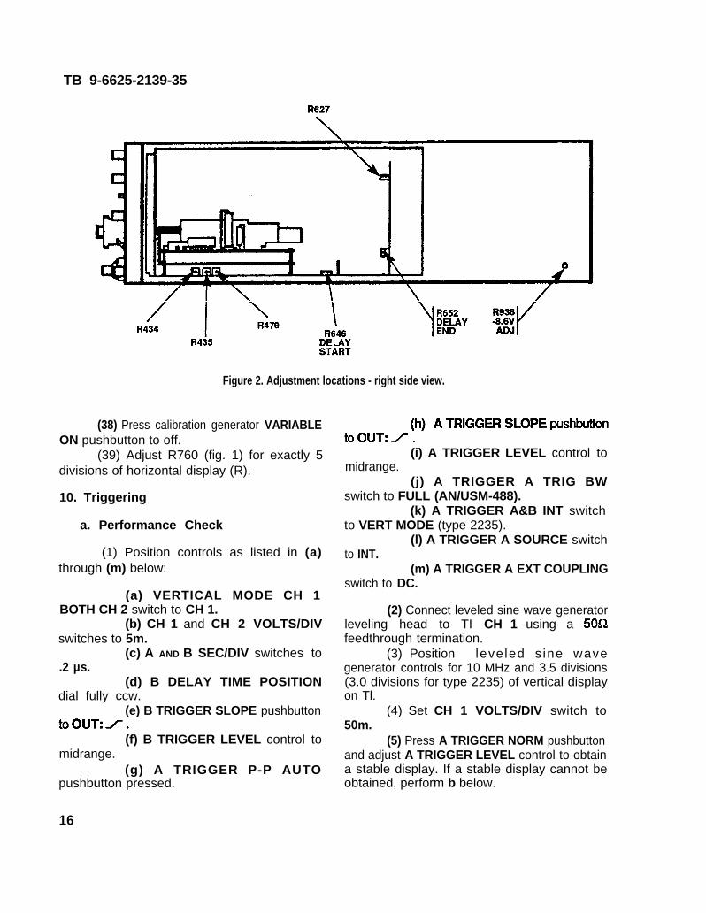
TB 9-6625-2139-35
Figure 2. Adjustment locations - right side view.
(38) Press calibration generator VARIABLEON pushbutton to off.
(39) Adjust R760 (fig. 1) for exactly 5divisions of horizontal display (R).
10. Triggering
a. Performance Check
(1) Position controls as listed in (a)through (m) below:
(a) VERTICAL MODE CH 1BOTH CH 2 switch to CH 1.
(b) CH 1 and CH 2 VOLTS/DIVswitches to 5m.
(c) A AND B SEC/DIV switches to.2 µs.
(d) B DELAY TIME POSITIONdial fully ccw.
(e) B TRIGGER SLOPE pushbutton
(f) B TRIGGER LEVEL control tomidrange.
(g) A TRIGGER P-P AUTOpushbutton pressed.
16
toOUT:/:-(i) A TRIGGER LEVEL control to
midrange.(j) A TRIGGER A TRIG BW
switch to FULL (AN/USM-488).(k) A TRIGGER A&B INT switch
to VERT MODE (type 2235).(l) A TRIGGER A SOURCE switch
to INT.(m) A TRIGGER A EXT COUPLING
switch to DC.
(2) Connect leveled sine wave generatorleveling head to TI CH 1 using a 50S2feedthrough termination.
(3) Position leve led s ine wavegenerator controls for 10 MHz and 3.5 divisions(3.0 divisions for type 2235) of vertical displayon Tl.
(4) Set CH 1 VOLTS/DIV switch to50m.
(5) Press A TRIGGER NORM pushbuttonand adjust A TRIGGER LEVEL control to obtaina stable display. If a stable display cannot beobtained, perform b below.

(6) Repeat technique of (5) above forA TRIGGER pushbutton combinations listed intable 9. If a stable display cannot be obtainedfor each combination, perform b below.
Table 9. A Triggger
ITest instrument
A TRIGGER pushbutton combinations I
Mode SLOPE
NORM IN: \
P-P AUTO IN: \
P-P AUTO OUTZ
(7) Set HORIZONTAL MODE switchto B. Adjust B INTENSITY control for suitableviewing.
(8) Verify a stable display can beobtained by adjusting B TRIGGER LEVELcontrol in a position other than B RUNSAFTER DLY; if not, perform b below.
(9) Press B TRIGGER SLOPEpushbutton to IN:> and repeat (8) above.
(10) Position controls as listed in (a)through (e) below:
(a) VERTICAL MODE CH 1BOTH CH 2 switch to CH 2.
(b) VERTICAL MODE TRIGGERSOURCE CH 1 pushbutton to out position (AN/USM-488).
(c) HORIZONTAL MODE switchto A.
(d) B TRIGGER SLOPE pushbuttonto Our:z .
(e) A TRIGGER A&B INT switchto CH 2 (type 2235).
(11) Repeat technique of (2) through (9)above for CH 2.
(12) Position controls as listed in (a)through (f) below:
(a) VERTICAL MODE CH 1BOTH CH 2 switch to CH 1
TB 9-6625-2139-35
(b) VERTICAL MODE TRIGGERSOURCE CH 1 and CH 2 pushbuttons toCOMPOSITE (AN/USM-488).
(c)to A.
(d).1 µs.
(e)to OUT: z .
(f)
HORIZONTAL MODE switch
A AND B SEC/DIV switches to
B TRIGGER SLOPE pushbutton
A TRIGGER A&B INT switchto VERT MODE (type 2235).
(13) Connect leveled sine wave generatorleveling head to TI CH 1 using a 50Qfeedthrough termination.
(14) Position leveled sine wave generatorcontrols for 60 MHz and 1.0 division of verticaldisplay on Tl.
(15) Repeat (5) through (9) above.
(16) Position controls as listed in (a)through (c) below:
(a) VERTICAL MODE CH 1BOTH CH 2 switch to CH 2.
(b) HORIZONTAL MODE switchto A.
(c) B TRIGGER SLOPE pushbuttonto OUT:Z .
(17) Repeat technique of (13) through(15) above for CH 2.
(18) Position controls as listed in (a)through (d) below:
(a) VERTICAL MODE CH 1BOTH CH 2 switch to CH 1.
(b) HORIZONTAL MODE switchto A.
17

TB 9-6625-2139-35
(c) A AND B SEC/DIV switches to.05 µs.
(d) B TRIGGER SLOPE pushbuttonto OUT:Y .
(19) Connect leveled sine wave generatorleveling head to TI CH 1 using a 50S2feedthrough termination.
(20) Position leveled sine wave generatorcontrols for 100 MHz and 1.5 divisions ofvertical display on Tl.
(21 ) Repeat (5) through (9) above.(22) Position controls as listed in (a)
through (c) below:
(a) VERTICAL MODE CH 1BOTH CH 2 switch to CH 2.
(b) HORIZONTAL MODE switchto A.
(c) B TRIGGER SLOPE pushbuttonto OUT:/;
(23) Repeat technique of (19) through(21 ) above for CH 2.
(24) Position controls as listed in (a)through (d) below:
(a) VERTICAL MODE CH 1BOTH CH 2 switch to CH 1.
(b) HORIZONTAL MODE switchto A.
(c) A TRIGGER NORM pushbuttonpressed.
(d) A TRIGGER A SOURCE switchto EXT.
(25) Connect leveled sine wavegenerator leveling head to TI EXT INPUT usinga 50f2 feedthrough termination.
(26) Position leveled sine wavegenerator controls for a 35 mV, 10 MHz output.
(27) Press in and hold TRIG VIEWpushbutton and adjust A TRIGGER LEVELcontrol to obtain a stable display.
(28) Repeat technique of (27) above forA TRIGGER pushbutton combinations listed intable 9.
(29) Release TRIG VIEW pushbutton.(30) Pull X10 CAL control to out position
and press A TRIGGER NORM pushbutton.(31 ) Position leveled sine wave generator
controls for a 120 mV, 60 MHz output.(32) Repeat (27) through (29) above.(33) Position leveled sine wave
generator controls for a 150 mV (200 mV fortype 2235), 100 MHz output.
(34) Press A TRIGGER NORM pushbuttonand repeat (27) through (29) above.
b. Adjustments.
(1) Disconnect leveled sine wavegenerator leveling head and 50!2 feedthroughtermination from Tl.
(2) Position controls as listed in (a)through (o) below:
(a) POSITION controls to midrange.(b) VERTICAL MODE CH 1
BOTH CH 2 switch to BOTH.(c) VERTICAL MODE TRIGGER
SOURCE CH 1 pushbutton to out position (AN/USM-488).
(d) VERTICAL MODE TRIGGERSOURCE CH 2 pushbutton to in position (AN/USM-488).
(e) VERTICAL MODE ADD ALTCHOP switch to ALT.
(f) CH 1 and CH 2 VOLTS/`DIVswitches to .5.
(g) CH 1 and CH 2 AC GND DCswitches to GND.
(h) HORIZONTAL MODE switchto A.
(i) A AND B SEC/DIV switches to1 ms.
(j) B TRIGGER SLOPE toOUT:/ .
(k) B TRIGGER LEVEL control tomidrange.
( l ) A TRIGGER P-P AUTOpushbutton pressed.
18

TB 9-6625-2139-35
(m) A TRIGGER SLOPE pushbutton (a) VERTICAL MODE CH 1to OUT:/. BOTH CH 2 switch to CH 1.
(n) A TRIGGER LEVEL control to (b) VERTICAL MODE TRIGGERmidrange. SOURCE CH 1 pushbutton to in position (AN/
(o) A TRIGGER A&B INT switch USM-488).to CH 2 (type 2235). (c) VERTICAL MODE TRIGGER
(3) Adjust CH 1 and CH 2 POSITIONcontrols to set both traces to the centerhorizontal graticule line.
(4) Connect digital multimeter LO tochassis ground and HI to pin 1 on A5 (fig. 1)board connector. Digital multimeter indicationwill be less than 100 mV dc. Record digitalmultimeter indication.
(5) Position controls as listed in (a)through’(c) below:
. .
SOURCE CH2 pushbutton to out position (AN/USM-488).
(d) CH 1 VOLTS/DIV switch to .1.(e) CH 1 AND CH 2 AC GND DC
switches to AC.(f) A AND B SEC/DIV switches to
10 µs.(9) A TRIGGER A&B INT switch
to CH 1 (type 2235).
(11 ) Connect leveled sine wave generator(a) VERTICAL MODE TRIGGER leveling head to TI CH 1 using- a 50S2
SOURCE CH 1 pushbutton to in position (AN/ feedthrough termination.USM-488). (12) Position leveled sine wave generator
(b) VERTICAL MODE TRIGGER controls for 50 kHz and 2.2 divisions of verticalSOURCE CH 2 pushbutton to out position (AN/ display on Tl.USM-488). (13) Set CH 1 VOLTS/DIV switch to 1.
(c) A TRIGGER A&B INT switch (14) Adjust R479 (fig. 2) while rotating Ato CH 1 (type 2235). TRIGGER LEVEL control slowly so that the A
(6) Adjust R309 (fig. 1) for digitalmultimeter indication recorded in (4) above.
(7) Position controls as listed in (a)through (c) below:
(a) VERTICAL MODE TRIGGERSOURCE CH 1 pushbutton to out position (AN/USM-488).
(b) VERTICAL MODE TRIGGERSOURCE CH 2 pushbutton to in position (AN/USM-488).
(c) A TRIGGER A&B INT switchto CH 2 (type 2235).
(8) Repeat (4) through (7) above untildigital multimeter indications in (4) and (6)above are equal within ±1 mV dc.
(9) Disconnect digital multimeter.(10) Position controls as listed in (a)
through (g) below:
trigger is just able to be maintained (R).(15) Set CH 1 VOLTS/DIV switch to
50m and adjust A TRIGGER LEVEL controlfully cw.
(16) Position leveled sine wave generatoramplitude controls for 5 divisions of verticaldisplay on Tl.
(17) Set CH 1 VOLTS/DIV switch to .5.(18) Adjust R434 (fig. 2) so that the
display just solidly triggers on positive peak ofsignal (R).
(19) Press A TRIGGER SLOPEpushbut ton to IN:> and ad jus t ATRIGGER LEVEL control fully CCW.
(20) Adjust R435 (fig. 2) so that thedisplay just solidly triggers on the negativepeak of signal (R).
(21) Connect leveled sine wavegenerator leveling head to one side of a BNCtee. Connect BNC tee to TI CH 1 using an Xl0
19

TB 9-6625-2139-35
attenuator and a 50Q feedthrough termination.Connect the other side of BNC tee to TI EXTINPUT.
(22) Set CH 1 VOLTS/DIV switch to10m and A TRIGGER A SOURCE switch toEXT.
(23) Position leveled sine wave generatoramplitude controls for 2.2 divisions of verticaldisplay on Tl.
(24) Adjust A TRIGGER LEVEL controlfor a stable display.
(25) Set HORIZONTAL MODE switchto B and adjust B TRIGGER LEVEL control fora stable display.
(26) Set CH 1 VOLTS/DIV switch to .1.(27) Adjust R627 (fig. 2) so that a
display can just be maintained by adjusting BTRIGGER LEVEL control (R).
11. Calibrator Amplitude
(a) Performance Check
(1) Position controls as listed in (a)through (n) below:
(a) POSITION controls tomidrange.
(b) VERTICAL MODE CH 1BOTH CH 2 switch to CH 1.
(c) VERTICAL MODE TRIGGERSOURCE CH 1 and CH 2 pushbuttons toCOMPOSITE (AN/USM-488).
(d) CH 1 VOLTS/DIV switch to .1.(e) CH 1 AC GND DC switch to
DC.(f) HORIZONTAL MODE switch
to A.(g) A AND B SEC/DIV switches to
.5 ms.(h) Xl0 CAL control to in position.( i ) A TRIGGER P-P AUTO
pushbutton pressed.(j) A TRIGGER SLOPE pushbutton
to Olmx .(k) A TRIGGER LEVEL control to
midrange.
(l) A TRIGGER A TRIG BWswitch to FULL (AN/USM-488).
(m) A TRIGGER A&B INT switchto VERT MODE (type 2235).
(n) A TRIGGER A SOURCE switchto INT.
(2) Connect calibration generatorOUTPUT to TI CH 1 using comparator.
(3) Connect TI AMP CAL (PROBEADJUST on type 2235) to comparator FROMDUT CALIBRATOR.
(4) Set comparator INTERNALTERMINATION switch to OPEN and pressDUT pushbutton.
(5) Adjust A TRIGGER LEVEL andCH 1 and horizontal POSITION controls, asnecessary, to view waveform.
(6) Note waveform amplitude.(7) Position calibration generator
controls for AMPL MODE VOLT, VARIABLEON, and a.5 V, 1kHz output.
(8) Press comparator CG pushbuttonand repeat (5) above.
(9) Adjust calibration generator VARcontrol for waveform amplitude noted in (6)above. If calibration generator error readoutindication is not within ±2% (±5% for type2235), perform b below.
b. Adjustments
(1) Press calibration generatorVARIABLE ON pushbutton to off.
(2) Note waveform amplitude.
(3) Press comparator DUT pushbuttonand adjust TI CH 1 POSITION control to viewwaveform.
(4) Adjust R984 (fig. 1) for waveformamplitude noted in (2) above (R).
(5) Press comparator CG pushbuttonand adjust TI CH 1 POSITION control to viewwaveform.
(6) Repeat (2) through (5) above asnecessary.
20

TB 9-6625-2139-35
12. Power Supply 13. Final Procedure
a. Performance Check. Connect digitalmultimeter LO to chassis ground and HI toTP961 -8.6 (fig. 1). If digital multimeter a. Deenergize and disconnect all
indication is not between -8.56 and -8.64 V dc, equipment.perform b below.
b. Adjustments. Adjust R938 -8.6V ADJ(fig. 2) for a -8.60 V dc indication on digital b. Annotate and affix Label/Form in
multimeter (R). accordance with TB 750-25.
21
TM 11-6625-31 35-24P
0
TECHNICAL MANUAL
.
.
.
.
ORGANIZATIONAL, DIRECT SUPPORT, ANDGENERAL SUPPORT MAINTENANCE
REPAIR PARTS AND SPECIAL TOOLS LISTFOR
‘ OSCILLOSCOPE AN /USM=488(NSN 6625=01 -1 87-7847)
@ HEADQUARTERS, DEPARTMENT OF THE ARMY12 SEPTEMBER 1985

TM 11-6625-3135-24
Technical Manual
No. 11-6625-3135-24P
HEADQUARTERSDEPARTMENT OF THE ARMY
Washington, DC, 12 September 1985
ORGANIZATIONAL, DIRECT SUPPORT, ANDGENERAL SUPPORT MAINTENANCE
REPAIR PARTS AND SPECIAL TOOLS LISTFOR
OSCILLOSCOPE AN/USM-488(NSN 6625-01-187-7847)
Current as of 1 April 1985
REPORTING OF ERRORS AND RECOMMENDING IMPROVEMENTS
You can help improve this manual. If you find any mistakes or if you know of a way toimprove the procedures, please let us know. Mail your letter, DA Form 2028(Recommended Changes to Publications and Blank Forms), or DA Form 2028-2 locatedin the back of this manual direct to: Commander, US Army Communications-ElectronicsCommand and Fort Monmouth, ATTN: AMSEL-ME-MP, Fort Monmouth, NJ 07703-5007.A reply will be furnished to you.
TABLE OF CONTENTS
Section I.II.
G r o u p 0 001
Sect ion Ill.IV.
Page
Introduction . . . . . . . . . . . . . . . . . . . . . . . . . . . . . . . . . . . . . . . . . . . . . . . . . . . . . . . . . . . . . .Repair parts list . . . . . . . . . . . . . . . . . . . . . . . . . . . . . . . . . . . . .Oscilloscope AN/USM-488 . . . . . . . . . . . . . . . . . . . . . . . . . . . . . . . . . . . . . . . . 1-1Circuit card assembly A1 . . . . . . . . . . . . . . . . . . . . . . . . . . . . . . . . . . . . . . . . . . . . . . . ...2-1Special tools list (not applicable)National stock number and part number index . . . . . . . . . . . . . . . . . . . . . . . . . . . . . . . . l-1
IllusFigure
12
i / ( i i b l a n k )
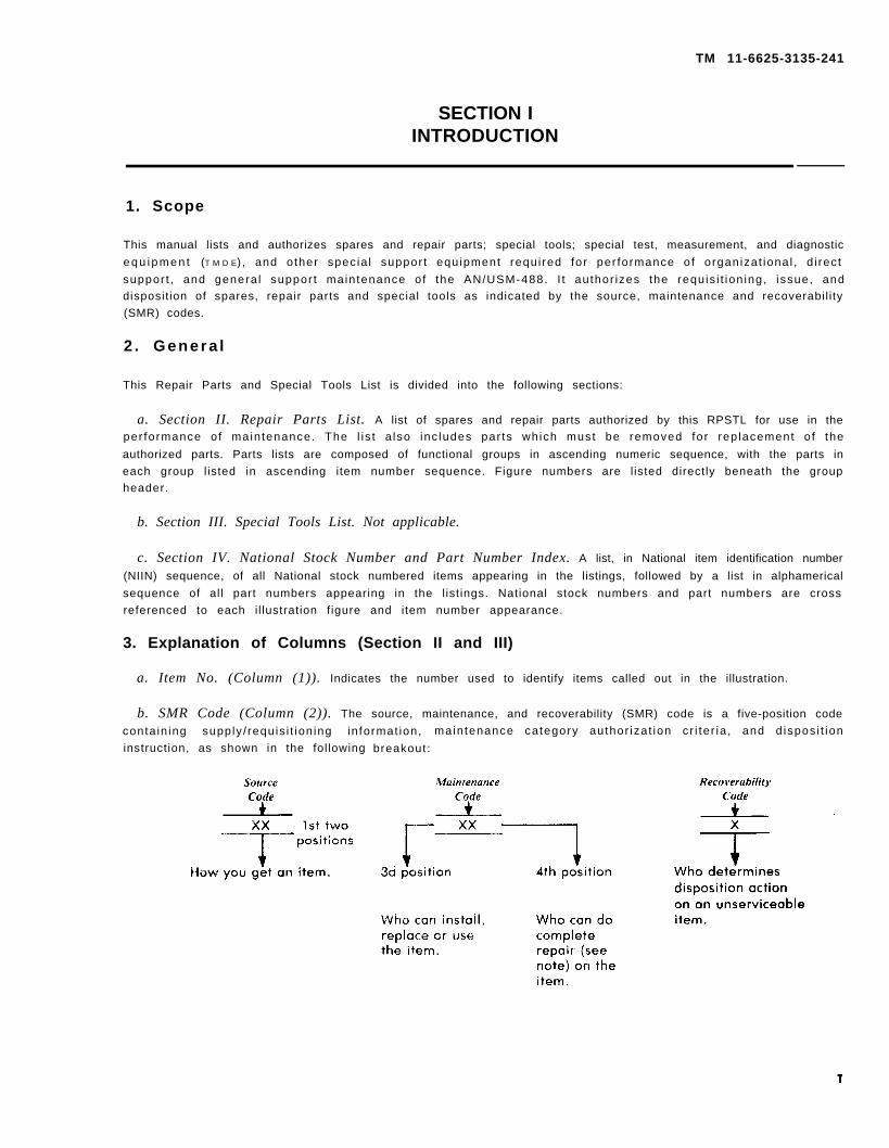
1
TM 11-6625-3135-241
SECTION IINTRODUCTION
1. Scope
This manual lists and authorizes spares and repair parts; special tools; special test, measurement, and diagnostic
e q u i p m e n t (T M D E) , and other spec ia l suppor t equ ipment requ i red for per formance of organizat iona l , d i rec t
suppor t , and genera l suppor t main tenance o f the AN/USM-488. I t au thor izes the requ is i t ion ing, issue, and
disposit ion of spares, repair parts and special tools as indicated by the source, maintenance and recoverabil i ty
(SMR) codes.
2 . Genera l
This Repair Parts and Special Tools List is divided into the following sections:
a. Section II. Repair Parts List. A list of spares and repair parts authorized by this RPSTL for use in the
per formance o f main tenance. The l i s t a lso inc ludes par ts wh ich must be removed for rep lacement o f the
authorized parts. Parts lists are composed of functional groups in ascending numeric sequence, with the parts in
each group l isted in ascending item number sequence. Figure numbers are l isted directly beneath the group
header.
b. Section III. Special Tools List. Not applicable.
c. Section IV. National Stock Number and Part Number Index. A list, in National item identification number
(NIIN) sequence, of all National stock numbered items appearing in the listings, followed by a list in alphamerical
sequence of al l part numbers appearing in the l ist ings. National stock numbers and part numbers are cross
referenced to each i l lustration figure and item number appearance.
3. Explanation of Columns (Section II and III)
a. Item No. (Column (1)). Indicates the number used to identify items called out in the illustration.
b. SMR Code (Column (2)). The source, maintenance, and recoverability (SMR) code is a five-position code
conta in ing supply / requis i t ion ing in format ion, main tenance category author iza t ion cr i te r ia , and d ispos i t ion
instruction, as shown in the following breakout:

TM 11-6625-3135-24P
NOTE
Complete repair: Maintenance capacity, capability, and authority to perform allcorrective maintenance tasks of the “Repair” function in a use/user environmentin order to restore serviceability to a failed item.
(1) Source Code. The source code tells you how to get an item needed for maintenance, repair, or overhaulof an end item/equipment. Explanations of source codes follows:
Code Explanation
Stocked items; use the applicable NSN to request/requisition items withthese source codes. They are authorized to the category indicatedby the code entered in the third position of the SMR code.
NOTE
Items coded PC are subject to deterioration.
Items with these codes are not to be requested/requisitioned individual-ly. They are part of a kit which is authorized to the maintenancecategory indicated in the third position of the SMR code. The completekit must be requisitioned and applied.
Items with these codes are not to be requested/requisitionedindividually. They must be made from bulk material which is identifiedby the part number in the description and usable on code (UOC)column and listed in the Bulk Material group of the repair parts list. Ifthe item is authorized to you by the third position code of the SMRcode, but the source code indicates it is made at a higher category,order the item from the higher category of maintenance.
ms with these codes are not to be requested/requisitioned individual-Iy. The parts that make up the assembled item must be requisitionedor fabricated and assembled at the category of maintenance indicatedby the source code. If the disposition code of the SMR code authorizesyou to replace the item, but the source code indicates the item isassembled at a higher category, order the item from the highercategory of maintenance.
XA - Do not requis i t ion an “XA” coded i tem. Order i t s nex t h igher as sembly .XB - If an “XB” item is not available from salvage, order it using the FSCM and part number given.XC - Installation drawing, diagram, instruction sheet, field service drawing, that is identified by
manufacturers part number.XD - Item is not stocked. Order an “XD” coded item through normal supply channels using the FSCM
and part number given, if no NSN is available.
2
TM 11-6625-3135-24P
NOTE
Cannibalization or controlled exchange, when authorized, may be used as asource of supply for items with the above source codes, except for those sourcecoded “XA” or those aircraft support i tems restricted by requirements ofAR 750-1.
(2) Maintenance Code. Maintenance codes tell you the category of maintenance authorized to USE andREPAIR support items. The maintenance codes are entered in the third and fourth positions of the SMR code asfollows:
(a) The maintenance code entered in the third posit ion tel ls you the lowest maintenance categoryauthorized to remove, replace, and use an item. The maintenance code entered in the third position will indicateauthorization to one of the following categories of maintenance.
Code Application/Explanation
C - Crew or operator maintenance done within organizational or aviation maintenance.O - Organizational or aviation unit category can remove, replace, and use the item.F - Direct support or aviation intermediate category can remove, replace, and use the item.
H - General support category can remove, replace, and use the item.L - Specialized repair activity can remove, replace, and use the item.
D - Depot category can remove, replace, and use the item.
(b) The maintenance code entered in the fourth position tells whether or not the item is to be repairedand identifies the lowest maintenance category with the capability to do complete repair (i. e., perform all
authorized repair functions). This position will contain one of the following maintenance codes:
NOTE
Some l imi ted repa i r may be done on the i tem at a lower category o fmaintenance, if authorized by the Maintenance Allocation Chart (MAC) and SMRcodes.
Code Application/Explanation
O - Organizational or aviation unit is the lowest category that can do complete repair of the item.F - Direct support or aviation intermediate is the lowest category that can do complete repair of
the item.
H - General support is the lowest category that can do complete repair of the item.L - Specialized repair activity (designate the specialized repair activity) is the lowest category that
can do complete repair of the item.D - Depot is the lowest category that can do complete repair of the item.z - Nonreparable. No repair is authorized.B - No repair is authorized. (No parts or special tools are authorized for the maintenance of a “B”
coded item. ) However, the item may be reconditioned by adjusting, lubricating, etc., at theuser category.
(3) Recoverability Code. Recoverability codes are assigned to items to indicate the disposition action onunserviceable items. The recoverability code is entered in the fifth position of the SMR Code as follows:
3

4
TM 11-6625-3135-24P
Recoverabilitycodes
Z -
O -
F -
H -
D -
L -
A -
Application/Explanation
Nonreparable item. When unserviceable, condemn and dispose of the item at the category ofmaintenance shown in the third position of SMR Code.
Reparable item. When uneconomically reparable, condemn and dispose of the item atorganizational or aviation unit category.
Reparable item. When uneconomically reparable, condemn and dispose of the item at thedirect support or aviation intermediate category.
Reparable item. When uneconomically reparable, condemn and dispose of the item at generalsupport category.
Reparable item. When beyond lower level repair capability, return to depot. Condemnation anddisposal of item not authorized below depot category.
Reparable item. Condemnation and disposal not authorized below specialized repair activity(SRA).
Item requires special handling or condemnation procedures because of specific reasons (e.g.,precious metal content, high dollar value, critical material, or hazardous material). Refer toappropriate manuals/directives for specific instructions.
c. FSCM (Column (3)). The Federal Supply Code for Manufacturer (FSCM) is a 5-digit numeric code which isused to identify the manufacturer, distributor, or Government agency, etc., that supplies the item.
d. Part Number (Column (4)). Indicates the primary number used by the manufacturer (individual, company,firm, corporation, or Government activity), which controls the design and characteristics of the item by means ofits engineering drawings, specifications, standards, and inspection requirements to identify an item or range ofitems.
NOTE
When you use a NSN to requisition an item, the item you receive may have adifferent part number from the part ordered.
e. Description and Usable on Code (UOC)(Column (5)). This column includes the following information.
(1) The Federal item name and, when required, a minimum description to identify the item.
(2) The statement “END OF FIGURE” appears just below the last item description in Column (5) for a given
figure in both section II and section III.
f. Qty (Column (6)). Indicates the quantity of the item used in the breakout shown on the illustration figure, which is prepared for a functional group, subfunctional group, or an assembly, A “V” appearing in this column inlieu of a quantity indicates that the quantity is variable and the quantity may vary from application to application.
4 . E x p l a n a t i o n o f C o l u m n s ( S e c t i o n I V )
a. National Stock Number (NSN) Index.
(1) Stock number column. This column l ists the NSN by National i tem identif ication number (NIIN)sequence. The NIIN consists of the last nine digits of the NSN. When using this column to locate an item, ignorethe first four digits of the NSN. When requisitioning items use the complete NSN (13 digits).
(2) Fig. co lumn. This column lists the number of the figure where the item is identified/located. Theillustrations are in numerical sequence in sections II and III.

TM 11-6625-3135-24P
(3) I tem co lumn. The item number identifies the item associated with the figure listed in the adjacent Fig.
column. This item is also identified by the NSN listed on the same line.
b. Part Number Index. Part numbers in this index are l isted by part number in ascending alphamericsequence.
(1) FSCM co lumn. This column lists the Federal supply code for manufacturer (FSCM)..
(2) Part number column. This column indicates the part number assigned to the item.
(3) Stock number column. This column lists the National stock number for the associated part number and
manufacturer identified in the part number and FSCM columns to the left.
(4) Fig. column. This column lists the number of the figure where the item is identified/located in sections
II and Ill.
(5) I tem co lumn. The item number is that number assigned to the item as it appears in the figure
referenced in the adjacent figure number column.
5. Special Information
a. Associated Publications. The publications listed below pertain to the AN/USM-488 and its components:
TM 11-6625-3135-12, Oscilloscope AN/USM-488
TM 11-6625-3135-40, Oscilloscope AN/USM-488
b. National Stock Numbers. National stock numbers (NSN’S) that are missing from P source coded items havebeen applied for and will be added to this TM by future change/revision when they are entered in the ArmyMaster Data File (AMDF). Until the NSN’S are established and published, submit exception requisitions to:Commander, US Army Communications-Electronics Command and Fort Monmouth, ATTN: AMSEL-MM, FortMonmauth, NJ 07703-5006 for the part required to support your equipment.
6. How to Locate Repair Parts
a. When National stock number or part number is not known.
(1) First. Using the table of contents, determine the assembly group or subassembly group to which the itembelongs. This is necessary since figures are prepared for assembly groups and subassembly groups, and listingsare divided into the same groups.
(2) Second. Find the figure covering the assembly group or subassembly group to which the item belongs.
(3) Third. Identify the item on the figure and note the item number.
(4) Fourth. Refer to the Repair Parts List for the figure to find the part number for the item number noted onthe figure.
(5) Fifth. Refer to the Part Number Index to find the NSN, if assigned.
5
6
TM 11-6625-3135-24P
(1) First. Using the Index of National stock numbers and part numbers, find the pertinent National stocknumber or part number. The NSN index is in National item identification number (NIIN) sequence (para 4a(1)). Thepart numbers in the part number index are listed in ascending alphameric sequence (para 4b). Both indexes cross-reference you to the illustration figure and item number of the item you are looking for.
(2) Second. After finding the figure and item number, verify that the item is the one you’re looking for, thenlocate the item number in the repair parts list for the figure.
7 . A b b r e v i a t i o n s
Not applicable.
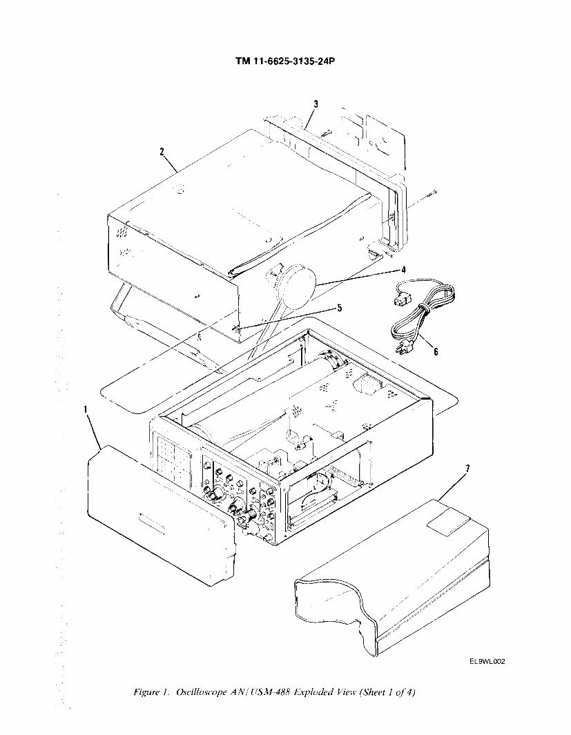
TM 11-6625-3135-24P
Figure 1.

TM 11-6625-3135-24P
Figure 1.

TM 11-6625-3135-24P
Figure 1.

TM 11-6625-3135-24P
Figure 1.

SECTION II TM11-6625-3135-24P PCN X43CXXC064R PAGE 134TM-CODE FS6
(1) (2) (3) (4) (5) (6)ITEM SMR PARTNO CODE FSCM NUMBER DESCRIPTION AND USABLE ON CODE (UOC) QTY
GROUP 00 OSCILLOSCOPE AN/USM-488
FIG 1
1 PAHZZ 80009 200-2520-00 COVER,OSCILLOSCOPE 12 PAHZZ 80009 390-0790-11 CABINET, OSCILLOSCOP 13 PAHZZ 80009 200-2538-00 COVER,REAR 14 PAHZZ 80009 367-0289-00 HANDLE,CARRYING 15 PAHZZ 80009 348-0659-01 FOOT,CABINET 26 PAHZZ 16428 CH8352 CABLE ASSY,PWR 17 PAHZZ 80009 016-0566-00 VISOR,CATHODE RAY T 18 PAHZZ 80009 426-1765-02 FRAME 19 PAHZZ 80009 378-0237-00 FILTER,MESH 110 PAHZZ 80009 337-2775-01 SHIELD,IMPLOSION 111 PAHZZ 80009 154-0861-00 ELECTRON TUBE 112 PAOZZ 80009 366-1391-03 KNOB 113 PAHZZ 80009 670-8418-00 CIRCUIT CARD ASSEMB 114 PAOZZ 80009 366-2146-03 KNOB 115 PAOZZ 80009 366-2049-01 KNOB 616 PAOZZ 80009 366-1146-00 KNOB 217 PAHZZ 73743 2X-20319-402 NUT,PLAIN,HEXAGON 118 PAHZZ 80009 136-0628-00 JACK,TIP 119 PAHZZ 80009 175-6140-00 CABLE ASSEMBLY,SPEC 120 PAHZZ 80009 311-2177-02 RESISTOR,VARIABLE N 121 PAHZZ 80009 384-1576-01 EXTENSION SHAFT 122 PAHZZ 12697 CM41773 RESISTOR,VARIABLE,N 123 PAHZZ 80009 670-8407-00 CIRCUIT CARD ASSEMB 124 PAHZZ 80009 670-8819-00 CIRCUIT CARD ASSEMB 125 PAHZZ 80009 311-1183-02 RESISTOR,VARIABLE W 126 PAHZZ 80009 358-0550-00 BUSHING,SHAFT 127 PAHZZ 8009 333-3109-00 PANEL,BLANK 128 PAHZZ 05129 461-S-70 DIAL,CONTROL 129 PAHZZ 80009 366-1850-00 KNOB 130 PAOZZ 80009 366-1840-03 KNOB 131 PAOZZ 80009 366-2052-01 KNOB 132 PAOZZ 80009 366-2148-01 KNOB 233 PAOZZ 80009 366-1031-03 KNOB 234 PAHZZ 80009 366-1480-03 PUSH BUTTON 135 PAHZZ 80009 384-1575-00 EXTENSION SHAFT 136 PAOZZ 80009 377-0512-00 INSERT,KNOB 637 PAHZZ 80009 214-3375-00 SWITCH,LEVER 238 PAHZZ 80009 672-0111-00 CIRCUIT CARD ASSEMB 139 PAHZZ 80009 119-1515-00 DELAY LINE 140 PAHZZ 80009 200-2519-00 CAP,CIRCUIT SOCKET 141 PAHZZ 78189 211-041800-00 NUT,PLAIN,ASSEMBLED 542 PAHZZ 80009 670-7615-00 CIRCUIT CARD ASSEMB 143 PAHZZ 80009 344-0132-00 CLIP,SPRING TENSION 144 PAHZZ 80009 348-0555-00 GROMMET,PLASTIC 145 PAHZZ 80009 344-0347-00 CLIP,ELECTRICAL 146 PAHZZ 13511 31-279 CONNECTOR,RECEPTACL 247 PAHZZ 80009 204-0833-00 FUSEHOLDER,EXTRACTO 148 PAOZZ 81349 F03B250V1A FUSE,CARTRIDGE 2
1-1

SECTION II TM11-6625-3135-24P PCN X43CXXC064R PAGE 135TM-CODE FS6
(1) (2) (3) (4) (5) (6)ITEM SMR PARTNO CODE FSCM NUMBER DESCRIPTION AND USABLE ON CODE (UOC) QTY
49 PAHZZ 80009 200-2264-00 CAP,FUSEHOLDER 150 PAHZZ 80009 119-1788-00 LINE FILTER ASSEMBL 151 PAHZZ 80009 195-0389-00 LEAD,ELECTRICAL 152 PAHZZ 54583 ZUB2203-00 RADIO FREQUE 153 PAHZZ 80009 195-5499-00 LEAD,ELECTRICAL 154 PAHZZ 78189 1224-02 WASHER,LOCK 155 PAHZZ 80009 200-1388-03 COVER,FUSE 156 PBHHH 80009 670-8404-00 CIRCUIT CARD ASSEMB 157 PAHZZ 80009 670-8405-00 CIRCUIT CARD ASSEMB 158 PAHZZ 80009 670-8406-00 CIRCUIT CARD ASSEMB 159 PAHZZ 80009 366-2013-00 PUSH BUTTON 1060 PAHZZ 80009 670-8444-00 CIRCUIT CARD ASSEMB 161 PAHZZ 80009 129-0999-00 SPACER,POST 262 PAHZZ 80009 131-2844-00 CONTACT,ELECTRICAL 163 PAHZZ 77820 9663-1 NT-34 CONNECTOR 264 PAHZZ 80009 010-6122-01 PROBE,VOLTAGE 265 PAHZZ 80009 013-0107-04 TIP,PROBE 266 PAHZZ 80009 195-1870-00 LEAD,ELECTRICAL 267 PAHZZ 80009 195-6176-00 LEAD,ELECTRICAL 268 PAHZZ 80009 175-3217-00 CABLE ASSEMBLY,RADI 269 PAHZZ 95712 33600-1 SHELL,ELECTRICAL CO 270 PAHZZ 80009 010-6101-03 LEAD,TEST 171 PAHZZ 80009 175-0124-01 LEAD,ELECTRICAL 172 PAHZZ 80009 175-0125-01 LEAD,ELECTRICAL 173 PAOZZ 80009 010-6101-02 LEAD,TEST 174 PAOZZ 80009 015-0201-04 COVER,TEST PROD 175 PAHZZ 80009 175-1661-01 CABLE ASSEMBLY,RADI 176 PAOZZ 24931 28P224-1 PROBE SUBASSEMBLY 177 PAOZZ 80009 206-0191-03 TIP,TEST PROD 178 PAHZZ 95712 2048-2NT34 ADAPTER,CONN 1
END OF FIGURE
1-2


TM 11-6625-3135-24P
Figure 2.
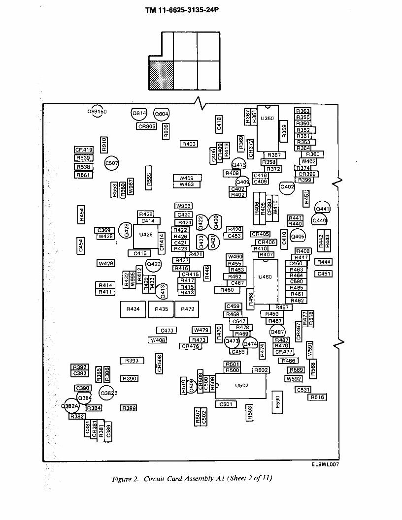
TM 11-625-3135-24P
FIGURE 2.
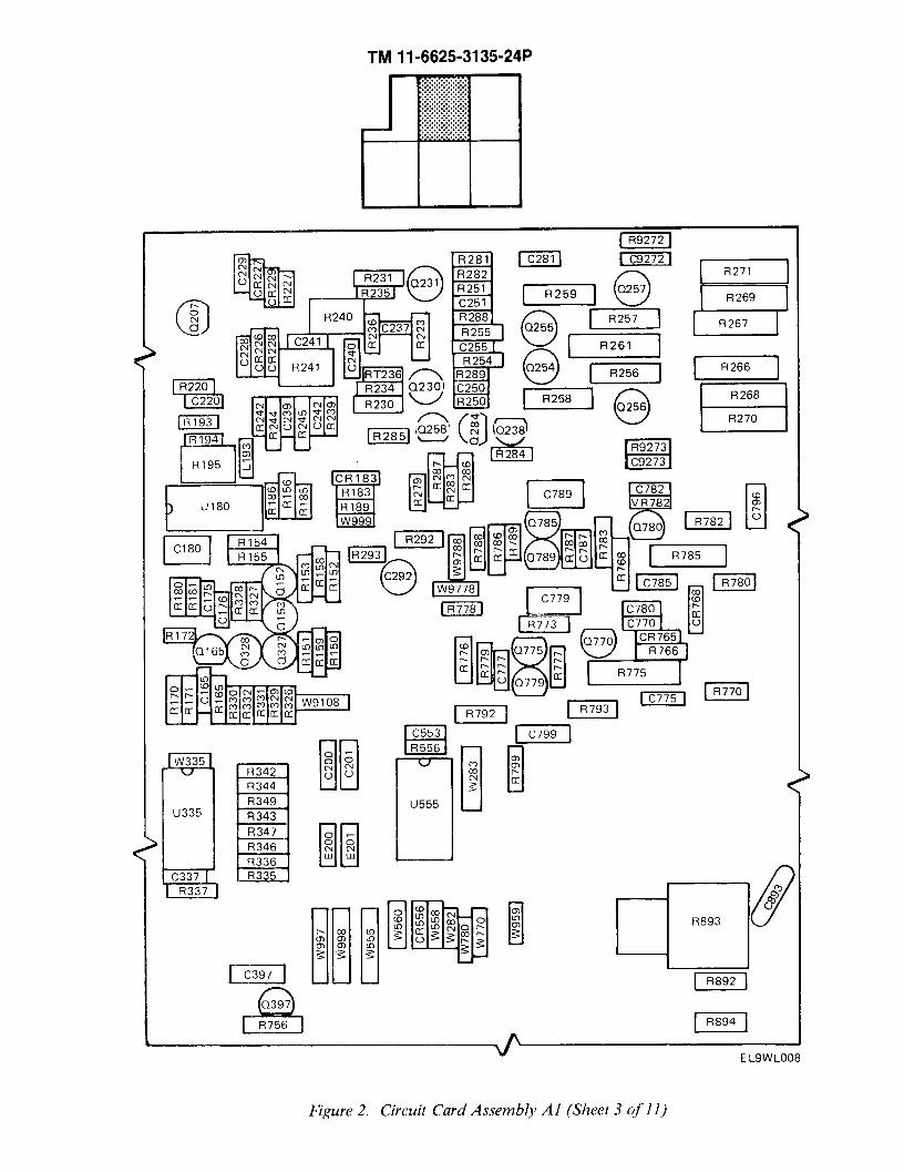
TM 11-6625-3135-24P
FIGURE 2.

TM 11-625-3135-24P
Figure 2.

TM 11-6625-3135-24P
Figure 2.

TM 11-6625-3135-24P
FIGURE 2.

TM 11-6625-3135-24P
Figure 2.

TM 11-6625-3135-24P
FIGURE 2.

TM 11-6625-3135-24P
Figure 2.
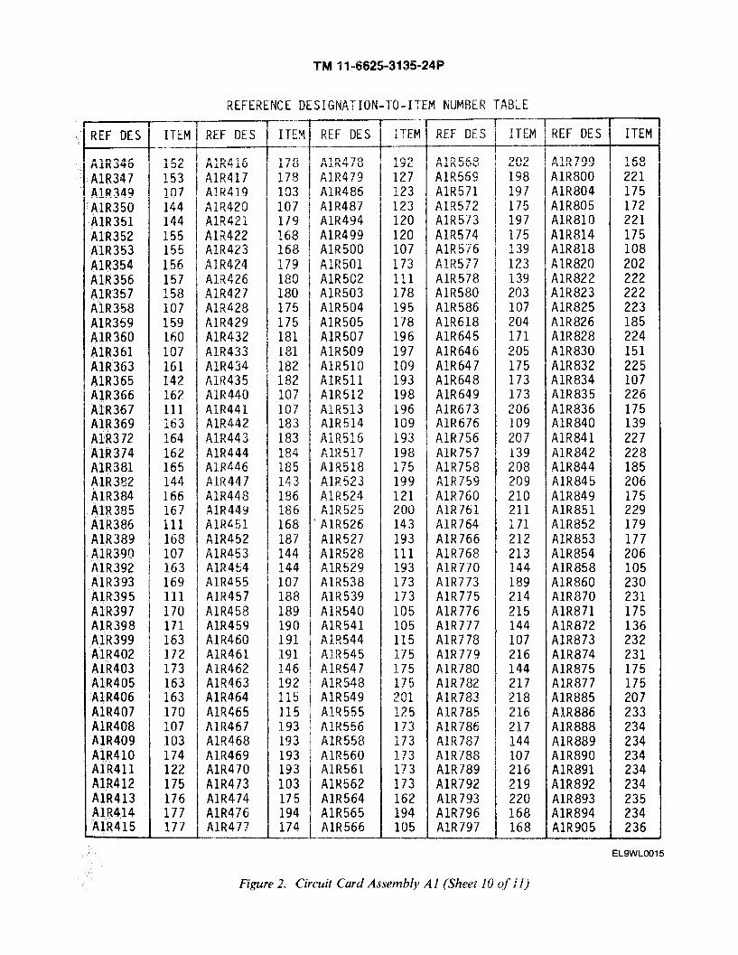
TM 11-6625-3135-24P
Figure 2.
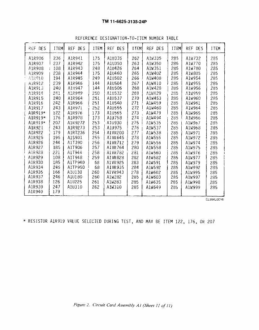
TM 11-6625-3135-24P
Figure 2.
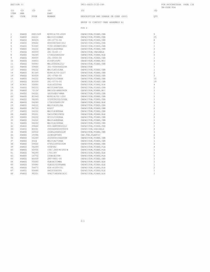
SECTION II TM11-6625-3135-24P PCN X43CXXC064R PAGE 136TM-CODE FS6
(1) (2) (3) (4) (5) (6)ITEM SMR PARTNO CODE FSCM NUMBER DESCRIPTION AND USABLE ON CODE (UOC) QTY
GROUP 01 CIRCUIT CARD ASSEMBLY A1
FIG 2
1 PAHZZ DD81349 M39014/05-2228 CAPACITOR,FIXED,CER 62 PAHZZ 04222 MA101C102MAR CAPACITOR,FIXED,CER 253 PAHZZ 80009 281-0772-00 CAPACITOR,FIXED,CER 84 PAHZZ 59660 805534Y5D0152J CAPACITOR,FIXED,CER 25 PAHZZ 51642 T150-050NP0180J CAPACITOR,FIXED,CER 16 PAHZZ 04222 MA101A680KAA CAPACITOR,FIXED,CER 37 PAHZZ 80009 281-0140-// CAPACITOR,VARIABLE 28 PAHZZ 56289 173D225X0020V CAPACITOR,FIXED,ELE 39 PAHZZ 80009 281-0500-00 CAPACITOR,FIXED,CER 110 PAHZZ 00853 D155F191F0 CAPACITOR,FIXED,MIC 211 PAHZZ 54583 MA12C0G2A121J CAPACITOR,FIXED,CER 112 PAHZZ 59660 301-000C0G0220K CAPACITOR 113 PAHZZ 04222 MA101A510JAA CAPACITOR,FIXED,CER 114 FAHZZ 81349 M39014/05-2237 CAPACITOR,FIXED,CER 215 PAHZZ 80009 281-0768-00 CAPACITOR,FIXED,CER 316 PAHZZ 04222 MA201C103KAA CAPACITOR,FIXED,CER 1017 PAHZZ 80009 281-0775-00 CAPACITOR,FIXED,CER 1918 PCHZZ 55680 ULA1A220TEA CAPACITOR,FIXED,ELE 419 PAHZZ 04222 MA101A4R7DAA CAPACITOR,FIXED,CER 220 PAHZZ 72136 DM15CD16R8D04CR CAPACITOR,FIXED,MIC 121 PAHZZ 04222 5R305SE474MAA CAPACITOR,FIXED,CER 122 PAHZZ 81349 M39014/02-1350 CAPACITOR,FIXED,CER 123 PAHZZ 56289 1C20C0G332J100B CAPACITOR,FIXED,CER 124 PAHZZ 56289 173D335X9015V CAPACITOR,FIXED,ELE 525 PAHZZ 04222 MA101A181JAA CAPACITOR,FIXED,CER 126 PAHZZ 96733 R3207 CAPACITOR,FIXED,CER 227 PAHZZ 04222 MA101A3R9DAA CAPACITOR,FIXED,CER 128 PAHZZ 90201 TAC105K035P02 CAPACITOR,FIXED,ELE 229 PAHZZ 04222 GC101C182KAA CAPACITOR,FIXED,CER 230 PAHZZ 04222 MA101A6R8DAA CAPACITOR,FIXED,CER 131 PAHZZ 04222 MA101A150KAA CAPACITOR,FIXED,CER 232 PAHZZ 59660 855-XXXY5E0222J CAPACITOR,FIXED,CER 133 PAHZZ 80031 2502A0R503VP02F0 CAPACITOR,VARIABLE 234 PAHZZ 20932 202EL200AT222K CAPACITOR,FIXED,CER 335 PAHZZ 19396 223K02PT485 CAP,FXD,PLASTIC 236 PAHZZ 56289 2C20Z5U104Z200B CAPACITOR,FIXED,CER 637 PAHZZ 0422 MA101A271KAA CAPACITOR,FIXED,CER 138 PAHZZ 59660 878521SY5S102M CAPACITOR,FIXED,CER 239 PAHZZ 56289 430P582 CAPACITOR,FIXED,PLA 440 PAHZZ 60935 158/.068/M/250/H CAPACITOR,FIXED,PLA 141 PAHZZ 56289 17D1149 CAPACITOR,FIXED,ELE 142 PAHZZ 14752 230B1E105K CAPACITOR,FIXED,PLA 143 PAHZZ 80009 283-0481-00 CAPACITOR,FIXED,CER 144 PAHZZ 55680 ULB1E101MEA CAPACITOR,FIXED,ELE 145 PAHZZ 55680 ULB1E102TFAANA CAPACITOR,FIXED,ELE 146 PAHZZ 54473 ECE-A100V10L CAPACITOR,FIXED,ELE 247 PAHZZ 55680 UHC2C330TFA CAPACITOR,FIXED,ELE 148 PAHZZ 90201 VPR271N040E1E1C CAPACITOR,FIXED,ELE 1
2-1

SECTION II TM11-6625-3135-24P PCN X43CXXC064R PAGE 137TM-CODE FS6
(1) (2) (3) (4) (5) (6)ITEM SMR PARTNO CODE FSCM NUMBER DESCRIPTION AND USABLE ON CODE (UOC) QTY
49 PAHZZ 90201 VPX841N012E1E1C CAPACITOR,FIXED,ELE 650 PAHZZ 59660 0301-080C0J0339C CAPACITOR,FIXED,CER 251 PAHZZ 80009 152-0141-02 SEMICONDUCTOR DEVIC 4752 PAHZZ 14433 G866 SEMICONDUCTOR DEVIC 153 PAHZZ 07263 FDH5004 SEMICONDUCTOR DEVIC 454 PAHZZ 81349 JAN1N3191 SEMICONDUCTOR DEVIC 455 PAHZZ 12969 UES1106 RECTIFIER,SEMICONDU 156 PAHZZ 07263 FDH2161 SEMICONDUCTOR DEVIC 157 PAHZZ 12969 UTR308 SEMICONDUCTOR DEVIC 858 PAHZZ 12969 UTR307 SEMICONDUCTOR DEVIC 259 PAHZZ 04713 1N5817 SEMICONDUCTOR DEVIC 260 PAHZZ 43944 A1B-3 LAMP,GLOW 361 PAHZZ 50434 HLMP3910 LIGHT EMITTING DIOD 162 PAHZZ 34899 2743001111 CORE,ELECTROMAGNET 363 PAHZZ 02114 56-590-65/4A6 CORE,ELECTROMAGNET 164 PAHZZ 56880 J41405-TC CORE,ELECTROMAGNET 165 PAHZZ 00779 5-3809509 CONNECTOR,RECEPTACL 366 PAHZZ 80009 108-0420-00 COIL,RADIO FREQUENC 467 PAHZZ 02113 B8724 COIL,RADIO FREQUENC 268 PAHZZ 22526 48283-036 TERMINAL,STUD 369 PAHZZ 22526 48283-029 CONTACT,ELECTRICAL 770 PAHZZ 04713 SPS8223 TRANSISTOR 1071 PAHZZ 80131 2N3904 TRANSISTOR 872 PAHZZ 04713 SRF 518 TRANSISTOR 273 PAHZZ 01295 SKA6664 TRANSISTOR 274 PAHZZ 04713 SPS8236 TRANSISTOR 275 PAHZZ 01281 LT4403 TRANSISTOR 476 PAHZZ 04713 SPS8317 TRANSISTOR 177 PAHZZ 04713 SPS8608M TRANSISTOR 478 PAHZZ 17856 J2012 SEMICONDUCTOR DEVIC 179 PAHZZ 04713 SPS8224 TRANSISTOR 780 PAHZZ 04713 SPS6868 TRANSISTOR 681 PAHZZ 04713 SPS6866K TRANSISTOR 582 PAHZZ 04713 SPS8246 TRANSISTOR 383 PAHZZ 80009 151-0276-00 TRANSISTOR 484 PAHZZ 04713 SPS8802-1 TRANSISTOR 185 PAHZZ 27014 T07391E2 TRANSISTOR 386 PAHZZ 80009 151-0347-00 TRANSISTOR 387 PAHZZ 04713 SPS6700 TRANSISTOR 388 PAHZZ 80009 151-0443-00 TRANSISTOR 189 PAHZZ 80009 151-0164-00 TRANSISTOR 290 PAHZZ 03508 C106B2X283 DIODE 191 PAHZZ 04713 SJE389 TRANSISTOR 292 PAHZZ 04713 MPT3N40 TRANSISTOR 193 PAHZZ 01121 CB4305 RESISTOR,FIXED,COMP 494 PAHZZ 81349 RNC55H4020FS RESISTOR,FIXED,FILM 495 PAHZZ 81349 RNC55K1100FS RESISTOR,FIXED,FILM 496 PAHZZ 91637 MFF1816G464R0F RESISTOR,FIXED,FILM 297 PAHZZ 8009 321-0223-0 RESISTOR,FIXED,FILM 298 PAHZZ 91637 CMF55116G19600F RES,FXD,FILM 299 PAHZZ 91637 CMF55116G21500F RES,FXD,FILM 4100 PAHZZ 91637 MFF1816G187R0F RESISTOR,FIXED,FILM 4
2-2

SECTION II TM11-6625-3135-24P PCN X43CXXC064R PAGE 138TM-CODE FS6
(1) (2) (3) (4) (5) (6)ITEM SMR PARTNO CODE FSCM NUMBER DESCRIPTION AND USABLE ON CODE (UOC) QTY
101 PAHZZ 81349 RCR07G820JS RESISTOR,FIXED,COMP 2102 PAHZZ 81349 RCR07G242JS RESISTOR,FIXED,COMP 3103 PAHZZ 81349 RCR07G182GS RESISTOR,FIXED,COMP 6104 PAHZZ 81349 RCR07G510JS RESISTOR,FIXED,COMP 4105 PAHZZ 01121 CB5115 RESISTOR,FIXED,COMP 6106 PAHZZ 81349 RCR07G111JS RESISTOR,FIXED,COMP 2107 PAHZZ 81349 RCR07G101JS RESISTOR,FIXED,COMP 23108 PAHZZ 81349 RCR07G302JS RESISTOR,FIXED,COMP 5109 PAHZZ 81349 RCR07G471JS RESISTOR,FIXED,COMP 6110 PAHZZ 73138 72-27-0 RESISTOR,VARIABLE,N 2111 PAHZZ 81349 RCR07G911JS RESISTOR,FIXED,COMP 6112 PAHZZ 81349 RNC60K6980FS RESISTOR,FIXED,FILM 2113 PAHZZ 81349 RNC55K82R5FS RESISTOR,FIXED,FILM 1114 PAHZZ 91637 MFF1816G274R0F RESISTOR,FIXED,FILM 2115 PAHZZ 01121 CB4315 RESISTOR,FIXED,COMP 6116 PAHZZ 91637 CMF55116G76R80F RESISTOR,FIXED,FILM 5117 PAHZZ 81349 RNC55K2490FS RESISTOR,FIXED,FILM 1118 PAHZZ 81349 RNC55K4870FS RESISTOR,FIXED,FILM 2119 PAHZZ 81349 RNC55H1130FS RESISTOR,FIXED,FILM 2120 PAHZZ 01121 CB33G5 RESISTOR,FIXED,COMP 3121 PAHZZ 81349 RNC55K2002FS RESISTOR,FIXED,FILM 3122 PAHZZ 80031 5043CX10K00J RESISTOR,FIXED,COMP RESISTOR R919 3
SELECTED BY TEST123 PAHZZ 81349 RCR07G221JS RESISTOR,FIXED,COMP 13124 PAHZZ 81349 RCR07G360JS RESISTOR,FIXED,COMP 2125 PAHYZZ 81349 RCR07G821JS RESISTOR,FIXED,COMP 3126 PAHZZ 73138 72-23-0 RESISTOR,VARIABLE,N 2127 PAHZZ 32997 3386X-T07-102 RESISTOR,VARIABLE,N 2128 PAHZZ 81349 RCR07G273JS RESISTOR,FIXED,COMP 1129 PAHZZ 81349 RNC55K6040FS RESISTOR,FIXED,FILM 2130 PAHZZ 91637 MFF1816G137R0F RESISTOR,FIXED,FILM 2131 PAHZZ 75042 CEBT0-6490F RES,FXD,FILM 2132 PAHZZ 81349 RNC60K7320FS RESISTOR,FIXED,FILM 2133 PAHZZ 91637 CMF65116G39R20F RES,FXD,FILM 1134 PAHZZ 81349 RCR07G151JS RESISTOR,FIXED,COMP 1135 PAHZZ 75042 CECT0-1500F RESISTOR,FIXED,FILM 6136 PAHZZ 81349 RCR07G223JS RESISTOR,FIXED,COMP 2137 PAHZZ 81349 RCR07G752JS RESISTOR,FIXED,COMP 1138 PAHZZ 80009 315-0621-00 RESISTOR 1139 PAHZZ 01121 CB5615 RESISTOR,FIXED,COMP 5140 PAHZZ 91637 CMF55116G49R90F RESISTOR,FIXED,FILM 2141 PAHZZ 81349 RNC55K7150FS RESISTOR,FIXED,FILM 1142 PAHZZ 81349 RCR07G620JS RESISTOR,FIXED,COMP 2143 PAHZZ 81349 RCR07G152JS RESISTOR,FIXED,COMP 6144 PAHZZ 81349 RCR07G470JS RESISTOR,FIXED,COMP 15145 PAHZZ 32997 3352T-CK5-501 RESISTOR,VARIABLE,W 1146 PAHZZ 81349 RNC55K1021FS RESISTOR,FIXED,FILM 3147 PAHZZ 81349 RNC55J1000FS RESISTOR,FIXED,FILM 2148 PAHZZ 81349 RNC55K5760FS RESISTOR,FIXED,FILM 4149 PAHZZ 81349 RNC60K1821FS RESISTOR,FIXED,FILM 2150 PAHZZ 91637 CMF55116G10000F RESISTOR,FIXED,FILM 2151 PAHZZ 81349 RNR60C1581FS RESISTOR,FIXED,FILM 3
2-3

SECTION II TM11-6625-3135-24P PCN X43CXXC064R PAGE 139TM-CODE FS6
(1) (2) (3) (4) (5) (6)ITEM SMR PARTNO CODE FSCM NUMBER DESCRIPTION AND USABLE ON CODE (UOC) QTY
152 PAHZZ 91637 CMF55116G14300F RES,FXD,FILM 2153 PAHZZ 81349 RNC55J2942FS RESISTOR,FIXED,FILM 2154 PAHZZ 80009 321-0203-00 RESISTOR,FIXED,FILM 2155 PAHZZ 80009 321-0274-00 RESISTOR,FIXED,FILM 2156 PAHZZ 81349 RCR07G272JS RESISTOR,FIXED,COMP 1157 PAHZZ 01121 CB6225 RESISTOR,FIXED,COMP 1158 PAHZZ 81349 RNC55K3480FS RESISTOR,FIXED,FILM 1159 PAHZZ 81349 RNC55K3400FS RESISTOR,FIXED,FILM 1160 PAHZZ 81349 RNC60K4120FS RESISTOR,FIXED,FILM 1161 PAHZZ 81349 RCR07G331JS RESISTOR,FIXED,COMP 1162 PAHZZ 57668 NTR25J-E02K0 RESISTOR,FIXED,COMP 3163 PAHZZ 57668 NTR25J-E750E RESISTOR,FIXED,COMP 5164 PAHZZ 81349 RCR07G220JS RESISTOR,FIXED,COMP 1165 PAHZZ 81349 RNC55K4123FS RESISTOR,FIXED,FILM 1166 PAHZZ 81349 RCR07G121JS RESISTOR,FIXED,COMP 2167 PAHZZ 01121 CB1305 RESISTOR,FIXED,COMP 1168 PAHZZ 81349 RCR07G100JS RESISTOR,FIXED,COMP 7169 PAHZZ 81349 RCR07G240JS RESISTOR,FIXED,COMP 1170 PAHZZ 011212 CB2005 RESISTOR,FIXED,COMP 2171 PAHZZ 57668 NTR25J-E200E RESISTOR,FIXED,COMP 3172 PAHZZ 81349 RCR07G562JS RESISTOR,FIXED,COMP 2173 PAHZZ 81349 RCR07G512JS RESISTOR,FIXED,COMP 13174 PAHZZ 81349 RCR07G132JS RESISTOR,FIXED,COMP 2175 PAHZZ 81349 RCR07G102JS RESISTOR,FIXED,COMP 21176 PAHZZ 01121 CB1135 RESISTOR,FIXED,COMP RESISTOR R919 1
SELECTED BY TEST177 PAHZZ 01121 CB2445 RESISTOR,FIXED,COMP 3178 PAHZZ 57668 NTR25J-E47K0 RESISTOR,FIXED,COMP 4179 PAHZZ 81349 RCR32G103JS RESISTOR,FIXED,COMP 5180 PAHZZ 57668 NTR25J-E430K RESISTOR,FIXED,COMP 2181 PAHZZ 81349 RCR07G823JS RESISTOR,FIXED,COMP 2182 PAHZZ 01121 E4A205 RESISTOR,VARIABLE,N 2183 PAHZZ 81349 RNC60K75R0FS RESISTOR,FIXED,FILM 2184 PAHZZ 01121 CB1625 RESISTOR,FIXED,COMP 1185 PAHZZ 81349 RCR07G104JS RESISTOR,FIXED,COMP 5186 PAHZZ 01121 CB2705 RESISTOR,FIXED,COMP 2187 PAHZZ 81349 RNC55K2210FS RESISTOR,FIXED,FILM 1188 PAHZZ 91637 MFF1816G316R0F RESISTOR,FIXED,FILM 1189 PAHZZ 81349 RNC60K7680FS RESISTOR,FIXED,FILM 2190 PAHZZ 81349 RNC55K7320FS RESISTOR,FIXED,FILM 1191 PAHZZ 81349 RNC55K2870FS RESISTOR FIXED FILM 2192 PAHZZ 81349 RNC60K1691FS RESISTOR,FIXED,FILM 2193 PAHZZ 813490 RCR07G392JS RESISTOR,FIXED,COMP 8194 PAHZZ 81349 RCR07G301JS RESISTOR,FIXED,COMP 3195 PAHZZ 01121 CB1245 RESISTOR,FIXED,COMP 2196 PAHZZ 81349 RC707G391JS RESISTOR,FIXED,COMP 2197 PAHZZ 81349 RCR07G222JS RESISTOR,FIXED,COMP 3198 PAHZZ 81349 RCR07G432JS RESISTOR,FIXED,COMP 3199 PAHZZ 01121 CB1535 RESISTOR,FIXED,COMP 1200 PAHZZ 81349 RNC55J2212FS RESISTOR,FIXED,FILM 1201 PAHZZ 57668 NTR25J-E680E RESISTOR,FIXED,COMP 1202 PAHZZ 80009 315-0332-00 RESISTOR,FIXED,COMP 2
2-4

SECTION II TM11-6625-3135-24P PCN X43CXXC064R PAGE 140TM-CODE FS6
(1) (2) (3) (4) (5) (6)ITEM SMR PARTNO CODE FSCM NUMBER DESCRIPTION AND USABLE ON CODE (UOC) QTY
203 PAHZZ 81349 RCR07G181JS RESISTOR,FIXED,COMP 1204 PAHZZ 81349 RNC55K2800FS RESISTOR,FIXED,FILM 1205 PAHZZ 32997 3352T-1-102 RESISTOR,VARIABLE,N 1206 PAHZZ 57668 NTR25J-E04K7 RESISTOR,FIXED,COMP 3207 PAHZZ 81349 RCR07G912JS RESISTOR,FIXED,COMP RESISTOR R919 2
SELECTED BY TEST208 PAHZZ 81349 RNC55K3092FS RESISTOR,FIXED,FILM 1209 PAHZZ 91637 CMF55116G59000F RES,FXD,FILM 1210 PAHZZ 32997 3352T-1-251 RESISTOR,VARIABLE,W 1211 PAHZZ 81349 RNC60K1501FS RESISTOR,FIXED,FILM 1212 PAHZZ 81349 RNC60K1330FS RESISTOR,FIXED,FILM 1213 PAHZZ 81349 RNC55K4320FS RESISTOR,FIXED,FILM 1214 PAHZZ 75042 CECT0-1652F RES,FXD,FILM 2215 PAHZZ 81349 RNC60K1331FS RESISTOR,FIXED,FILM 2216 PAHZZ 7668 NTR25J-E24K0 RESISTOR,FIXED,COMP 2217 PAHZZ 8009 321-0209-00 RESISTOR,FIXED,FILM 1218 PAHZZ 91637 CMF55116G12100F RESISTOR,FIXED,FILM 1219 PAHZZ 81349 RNC55K5361FS RESISTOR,FIXED,FILM 1220 PAHZZ 91637 MFF1816G56201F RESISTOR,FIXED,FILM 1221 PAHZZ 81349 RCR07G682JS RESISTOR,FIXED,COMP 3222 PAHZZ 57668 TR50J-E 5K1 RESISTOR,FIXED,COMP 2223 PAHZZ 81349 RC707G750JS RESISTOR,FIXED,COMP 1224 PAHZZ 81349 RCR07G560JS RESISTOR,FIXED,COMP 1225 PAHZZ 81349 RNC60K2001FS RESISTOR,FIXED,FILM 1226 PAHZZ 80009 321-0228-00 RESISTOR,FIXED,FILM 1227 PAHZZ 24546 NA60D2212F RES,FXD,FILM 1228 PAHZZ 01121 CB2415 RESISTOR,FIXED,COMP 1229 PAHZZ 32997 3352T-1-203 RESISTOR,VARIABLE,N 1230 PAHZZ 011212 CB6255 RESISTOR,FIXED,COMP 1231 PAHZZ 32997 3352T-1-104 RESISTOR,VARIABLE,N 2232 PAHZZ 81349 RCR07G513JS RESISTOR,FIXED,COMP 1233 PAHZZ 81349 RCR07G184JS RESISTOR,FIXED,COMP 1234 PAHZZ 57668 TR50J-E 510K RESISTOR,FIXED,COMP 6235 PAHZZ 011212 23M909 RESISTOR,VARIABLE,N 1236 PAHZZ 57668 TR50J-E82K RESISTOR,FIXED,COMP 2237 PAHZZ 91637 RS1A-90-R2J RESISTOR,FIXED,WIRE 1238 PAHZZ 57668 NTR25J-E39E0 RESISTOR 1239 PAHZZ 81349 RNC55K3570FS RESISTOR,FIXED,FILM 1240 PAHZZ 81349 RNC60K1002FS RESISTOR,FIXED,FILM 2241 PAHZZ 81349 RNC60K8452FS RESISTOR,FIXED,FILM 1242 PAHZZ 19701 5043CX510K0J RESISTOR,FIXED,COMP 1243 PAHZZ 01121 CB3035 RESISTOR,FIXED,COMP 2244 PAHZZ 01121 GB1545 RES,FXD,CMPSN 1245 PAHZZ 80009 308-0441-00 RESISTOR,FIXED,WIRE 1246 PAHZZ 81349 RNC55K2671FS RESISTOR,FIXED,FILM 1247 PAHZZ 81349 RNC55J1432FS RESISTOR,FIXED,FILM 1248 PAHZZ 57668 TR50J-E 4K7 RESISTOR,FIXED,COMP 1249 PAHZZ 57668 TR50J-E2K RESISTOR,FIXED,COMP 1250 PAHZZ 80009 308-0677-00 RESISTOR,FIXED,WIRE 1251 PAHZZ 01121 CB47G5 RESISTOR,FIXED,COMP 2252 PAHZZ 75042 BW200.620HM5PCT RESISTOR,FIXED,WIRE 1253 PAHZZ 57668 TR50J-E 120E RESISTOR,FIXED,COMP 2
2-5

SECTION II TM11-6625-3135-24P PCN X43CXXC064R PAGE 141TM-CODE FS6
(1) (2) (3) (4) (5) (6)ITEM SMR PARTNO CODE FSCM NUMBER DESCRIPTION AND USABLE ON CODE (UOC) QTY
254 PAHZZ 50157 2D1595 RESISTOR,THERMAL 1255 PAHZZ 31918 NE15/F2U103EE SWITCH,PUSH 1256 PAHZZ 54937 DMI 500-2044 TRANSFORMER,POWER 1257 PAHZZ 54937 5002573 TRANSFORMER,RADIO F 1258 PAHZZ 80009 120-1347-00 TRANSFORMER,RF 1259 PAHZZ 80009 120-1594-00 TRANSFORMER,POWER 1260 PAHZZ 80009 155-0274-00 MICROCIRCUIT,LINEAR 2261 PAHZZ 81349 M38510/10101BPC MICROCIRCUIT,LINEAR 1262 PAHZZ 02735 CA3102E-98 MICROCIRCUIT,LINEAR 2263 PAHZZ 02735 CA3127E-98 MICROCIRCUIT,LINEAR 1264 PAHZZ 18324 MC1458N MICROCIRCUIT,LINEAR 1265 PAHZZ 80009 234-0107-20 MICROCIRCUIT,LINEAR 1266 PAHZZ 04713 MC10198 MICROCIRCUIT,DIGITA 1267 PAHZZ 07263 96LS02 MICROCIRCUIT,DIGITA 1268 PAHZZ 04713 MC10H131 MICROCIRCUIT,DIGITA 1269 PAHZZ 04713 MC10H102 MICROCIRCUIT,DIGITA 1270 PAHZZ 04713 SN74LS132NDS MICROCIRCUIT,DIGITA 1271 PAHZZ 07263 74LS74A MICROCIRCUIT,DIGITA 1272 PAHZZ 01295 SN74LS09 MICROCIRCUIT,DIGITA 1273 PAHZZ 01295 SN74LS03 MICROCIRCUIT,DIGITA 1274 PAHZZ 27014 GLEA134 MICROCIRCUIT,LINEAR 1275 PAHZZ 01295 TL594CN MICROCIRCUIT,LINEAR 1276 PAHZZ 12969 CMX647 SEMICONDUCTOR DEVIC 1277 PAHZZ 04713 SZG35009K3 SEMICONDUCTOR DEVIC 1278 PAHZZ 04713 SZG20012 SEMICONDUCTOR DEVIC 2279 PAHZZ 04713 SZ13294RL SEMICONDUCTOR DEVIC 1280 PAHZZ 04713 SZG30214RL SEMICONDUCTOR,DEVIC 1281 PAHZZ 14552 TD3810983 SEMICONDUCTOR DEVIC 1282 PAHZZ 04713 SZG15RL SEMICONDUCTOR DEVIC 1283 PAHZZ 04713 SZ11738RL SEMICONDUCTOR DEVIC 1284 PAHZZ 04713 SZG35009K7 SEMICONDUCTOR DEVIC 1285 PAHZZ 57668 JWW-0200E0 LEAD,ELECTRICAL 57286 PAHZZ 80009 195-7065-00 LEAD,ELECTRICAL 1287 PAHZZ 80009 195-7064-00 LEAD,ELECTRICAL 1288 PAHZZ 80009 195-7063-00 LEAD,ELECTRICAL 1289 PAHZZ 80009 195-8235-00 LEAD,ELECTRICAL 1290 PAHZZ 80009 136-0830-00 SOCKET,PLUG IN ELEC 1291 PAHZZ 80009 200-2735-00 COVER,POWER SWITCH 1292 PAHZZ 80009 334-2363-00 MARKER,IDENTIFICATI 1293 PAHZZ 80009 175-6139-00 CABLE ASSEMBLY,SPEC 1294 PAHZZ 80009 342-0582-00 INSULATOR,PLATE 1295 PAHZZ 80009 343-1025-00 RETAINER,TRANSISTOR 1296 PAHZZ 80009 343-0969-00 RETAINER,TRANSISTOR 1297 PAHZZ 80009 342-0555-00 INSULATOR,PLATE 1298 PAHZZ 80009 407-2729-00 BRACKET,HEAT SINK 1299 PAHZZ 78189 211-041800-00 NUT,PLAIN,ASSEMBLED 3300 PAHZZ 80009 361-1047-00 SPACER,VARIABLE,RES 1301 PAHZZ 80009 175-6137-00 CABLE ASSEMBLY,SPEC 1302 PAHZZ 80009 175-6136-00 CABLE ASSEMBLY,SPEC 1303 PAHZZ 80009 198-4819-00 CABLE ASSEMBLY,SPEC 1304 PAHZZ 80009 175-6138-00 CABLE ASSEMBLY,SPEC 1305 PAHZZ 80009 175-2546-01 CABLE ASSEMBLY,SPEC 1
2-6

SECTION II TM11-6625-3135-24P PCN X43CXXC064R PAGE 142TM-CODE FS6
(1) (2) (3) (4) (5) (6)ITEM SMR PARTNO CODE FSCM NUMBER DESCRIPTION AND USABLE ON CODE (UOC) QTY
306 PAHZZ 80009 175-6141-00 CABLE ASSEMBLY,SPEC 1
END OF FIGURE
2-7


TM11-6625-3135-24P PCN X43CXXC074R PAGE 18SECTION IV TM-CODE FS6
NATIONAL STOCK NUMBER AND PART NUMBER INDEX
NATIONAL STOCK NUMBER INDEXSTOCK NUMBER FIG. ITEM STOCK NUMBER FIG. ITEM
5935-00-001-7558 1 46 5905-00-137-4277 2 1185905-00-055-6118 2 176 5905-00-138-1285 2 2255961-00-087-4063 2 54 5905-00-138-7530 2 945910-00-098-9281 2 14 5905-00-141-0742 2 2035961-00-103-6748 2 72 5905-00-141-0743 2 1935905-00-104-8362 2 174 5905-00-141-0744 2 1725905-00-104-8363 2 101 5905-00-141-1132 2 1375905-00-104-8368 2 144 5905-00-141-1183 2 1075961-00-105-7681 2 51 5910-00-163-3938 2 205905-00-105-7764 2 197 5905-00-163-7092 2 1875905-00-105-7768 2 139 5961-00-189-1266 2 745905-00-106-1248 2 184 5905-00-192-3461 2 1125905-00-106-1249 2 104 5310-00-197-4505 1 545905-00-106-1356 2 143 5310-00-231-4954 1 175905-00-106-3668 2 164 5905-00-233-9202 2 1905905-00-106-9357 2 223 5910-00-237-1196 2 345905-00-107-0656 2 168 5905-00-242-2546 2 1535905-00-110-0388 2 185 5905-00-247-2970 2 2455905-00-110-7620 2 175 5905-00-254-2451 2 1915905-00-110-7622 2 221 5905-00-258-5403 2 2085905-00-111-1679 2 173 5905-00-258-5882 2 2195905-00-111-4727 2 156 5905-00-259-4433 2 1465905-00-111-4750 2 194 5905-00-264-4330 2 1585905-00-112-7039 2 192 5999-00-275-0213 2 695905-00-113-4860 2 186 5905-00-284-6076 2 1595910-00-113-5499 2 22 5905-00-289-3920 2 2005905-00-114-0710 2 161 5905-00-305-7959 2 1195910-00-114-0805 2 15 5905-00-307-4104 2 955905-00-114-5343 2 103 5905-00-311-2351 2 2415905-00-114-5344 2 233 5905-00-346-8062 2 1485905-00-115-2261 2 207 5961-00-359-9493 2 875905-00-116-8556 2 136 5961-00-365-9935 2 865905-00-119-3504 2 128 5905-00-369-6931 2 1065905-00-119-8768 2 125 5905-00-372-0039 2 1515905-00-119-8811 2 134 5905-00-400-8999 2 935905-00-119-8812 2 166 5905-00-402-4258 2 2305905-00-120-9154 2 109 5961-00-404-5537 2 835910-00-121-7849 2 1 5905-00-405-7784 2 1885905-00-121-9932 2 196 5905-00-405-7790 2 965905-00-126-6692 2 142 5905-00-405-7803 2 1305905-00-126-6698 2 124 5961-00-417-4107 2 735905-00-126-6705 2 251 5905-00-419-2845 2 1475961-00-131-1196 2 53 5355-00-419-4032 1 165905-00-131-9729 2 108 5905-00-426-7129 2 1495905-00-133-0440 2 224 5905-00-426-7144 2 1835905-00-135-3972 2 170 5905-00-426-7708 2 975905-00-135-3973 2 123 5905-00-428-3857 2 2125905-00-136-3890 2 232 5905-00-431-7827 2 2175905-00-136-8406 2 102 5905-00-432-0370 2 2475905-00-136-8431 2 198 5905-00-432-0402 2 121
I-1
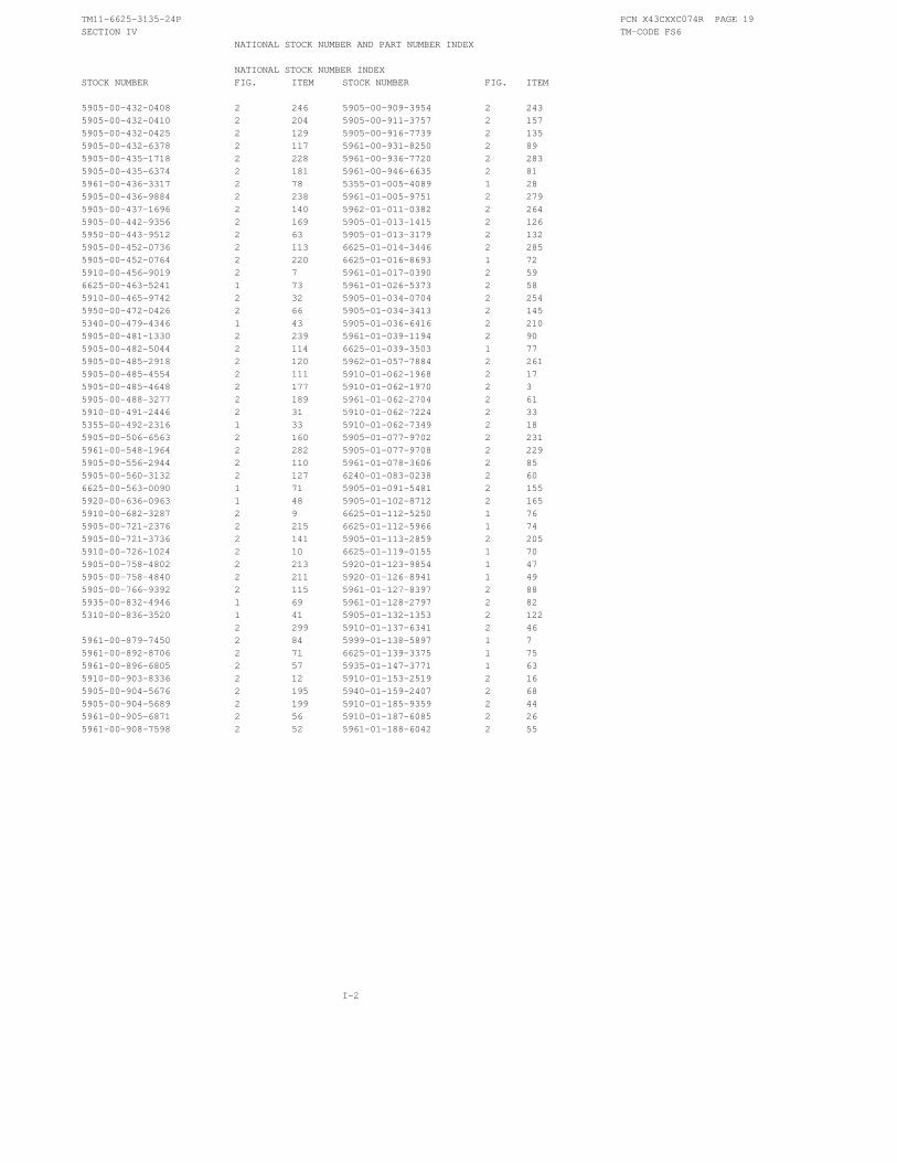
TM11-6625-3135-24P PCN X43CXXC074R PAGE 19SECTION IV TM-CODE FS6
NATIONAL STOCK NUMBER AND PART NUMBER INDEX
NATIONAL STOCK NUMBER INDEXSTOCK NUMBER FIG. ITEM STOCK NUMBER FIG. ITEM
5905-00-432-0408 2 246 5905-00-909-3954 2 2435905-00-432-0410 2 204 5905-00-911-3757 2 1575905-00-432-0425 2 129 5905-00-916-7739 2 1355905-00-432-6378 2 117 5961-00-931-8250 2 895905-00-435-1718 2 228 5961-00-936-7720 2 2835905-00-435-6374 2 181 5961-00-946-6635 2 815961-00-436-3317 2 78 5355-01-005-4089 1 285905-00-436-9884 2 238 5961-01-005-9751 2 2795905-00-437-1696 2 140 5962-01-011-0382 2 2645905-00-442-9356 2 169 5905-01-013-1415 2 1265950-00-443-9512 2 63 5905-01-013-3179 2 1325905-00-452-0736 2 113 6625-01-014-3446 2 2855905-00-452-0764 2 220 6625-01-016-8693 1 725910-00-456-9019 2 7 5961-01-017-0390 2 596625-00-463-5241 1 73 5961-01-026-5373 2 585910-00-465-9742 2 32 5905-01-034-0704 2 2545950-00-472-0426 2 66 5905-01-034-3413 2 1455340-00-479-4346 1 43 5905-01-036-6416 2 2105905-00-481-1330 2 239 5961-01-039-1194 2 905905-00-482-5044 2 114 6625-01-039-3503 1 775905-00-485-2918 2 120 5962-01-057-7884 2 2615905-00-485-4554 2 111 5910-01-062-1968 2 175905-00-485-4648 2 177 5910-01-062-1970 2 35905-00-488-3277 2 189 5961-01-062-2704 2 615910-00-491-2446 2 31 5910-01-062-7224 2 335355-00-492-2316 1 33 5910-01-062-7349 2 185905-00-506-6563 2 160 5905-01-077-9702 2 2315961-00-548-1964 2 282 5905-01-077-9708 2 2295905-00-556-2944 2 110 5961-01-078-3606 2 855905-00-560-3132 2 127 6240-01-083-0238 2 606625-00-563-0090 1 71 5905-01-091-5481 2 1555920-00-636-0963 1 48 5905-01-102-8712 2 1655910-00-682-3287 2 9 6625-01-112-5250 1 765905-00-721-2376 2 215 6625-01-112-5966 1 745905-00-721-3736 2 141 5905-01-113-2859 2 2055910-00-726-1024 2 10 6625-01-119-0155 1 705905-00-758-4802 2 213 5920-01-123-9854 1 475905-00-758-4840 2 211 5920-01-126-8941 1 495905-00-766-9392 2 115 5961-01-127-8397 2 885935-00-832-4946 1 69 5961-01-128-2797 2 825310-00-836-3520 1 41 5905-01-132-1353 2 122
2 299 5910-01-137-6341 2 465961-00-879-7450 2 84 5999-01-138-5897 1 75961-00-892-8706 2 71 6625-01-139-3375 1 755961-00-896-6805 2 57 5935-01-147-3771 1 635910-00-903-8336 2 12 5910-01-153-2519 2 165905-00-904-5676 2 195 5940-01-159-2407 2 685905-00-904-5689 2 199 5910-01-185-9359 2 445961-00-905-6871 2 56 5910-01-187-6085 2 265961-00-908-7598 2 52 5961-01-188-6042 2 55
I-2

TM11-6625-3135-24P PCN X43CXXC064R PAGE 20SECTION IV TM-CODE FS6
NATIONAL STOCK NUMBER AND PART NUMBER INDEX
NATIONAL STOCK NUMBER INDEXSTOCK NUMBER FIG. ITEM STOCK NUMBER FIG. ITEM
5910-01-189-9228 2 255910-01-191-9817 2 295961-01-192-0077 2 705961-01-192-1602 2 796625-01-197-1938 1 56
I-3

TM11-6625-3135-24P PCN X43CXXC084R PAGE 58SECTION IV TM-CODE FS6
NATIONAL STOCK NUMBER AND PART NUMBER INDEX
PART NUMBER INDEXFSCM PART NUMBER STOCK NUMBER FIG. ITEM
53944 A1B-3 6240-01-083-0238 2 6075042 BW200.620HM5PCT 2 25202113 B8724 2 6702735 CA3102E-98 2 26202735 CA3127E-98 2 26301121 CB1135 5905-00-055-6118 2 17601121 CB1245 5905-00-904-5676 2 19501121 CB1305 2 16701121 CB1535 5905-00-904-5689 2 19901121 CB1625 5905-00-106-1248 2 18401121 CB2005 5905-00-135-3972 2 17001121 CB2415 5905-00-435-1718 2 22801121 CB2445 5905-00-485-4648 2 17701121 CB2705 5905-00-113-4860 2 18601121 CB3035 5905-00-909-3954 2 24301121 CB33G5 5905-00-485-2918 2 12001121 CB4305 5905-00-400-8999 2 9301121 CB4315 5905-00-766-9392 2 11501121 CB47G5 5905-00-126-6705 2 25101121 CB5115 2 10501121 CB5615 5905-00-105-7768 2 13901121 CB6225 5905-00-911-3757 2 15701121 CB6255 5905-00-402-4258 2 23075042 CEBT0-6490F 2 13175042 CECT0-1500F 5905-00-916-7739 2 13575042 CECT0-1652F 2 21416428 CH8352 1 691637 CMF55116G10000F 2 15091637 CMF55116G12100F 2 21891637 CMF55116G14300F 2 15291637 CMF55116G19600F 2 9891637 CMF55116G21500F 2 9991637 CMF55116G49R90F 5905-00-437-1696 2 14091637 CMF55116G59000F 2 20991637 CMF55116G76R80F 2 11691637 CMF65116G39R20F 2 13312969 CMX647 2 27612697 CM41773 1 2203508 C106B2X283 5961-01-039-1194 2 9054937 DMI 500-2044 2 25672136 DM15CD16R8D04CR 5910-00-163-3938 2 2000853 D155F191F0 5910-00-726-1024 2 1054473 ECE-A100V10L 5910-01-137-6341 2 4601121 E4A205 2 18207263 FDH2161 5961-00-905-6871 2 5607263 FDH5004 5961-00-131-1196 2 5381349 F03B250V1A 5920-00-636-0963 1 4801121 GB1545 2 24404222 GC101C182KAA 5910-01-191-9817 2 2927014 GLEA134 2 27414433 G866 5961-00-908-7598 2 52
I-4

TM11-6625-3135-24P PCN X43CXXC084R PAGE 59SECTION IV TM-CODE FS6
NATIONAL STOCK NUMBER AND PART NUMBER INDEX
PART NUMBER INDEXFSCM PART NUMBER STOCK NUMBER FIG. ITEM
50434 HLMP3910 5961-01-062-2704 2 6181349 JAN1N3191 5961-00-087-4063 2 5457668 JWW-0200E0 6625-01-014-3446 2 28517856 J2012 5961-00-436-3317 2 7856880 J41405-TC 2 6401281 LT4403 2 7504222 MA101A150KAA 5910-00-491-2446 2 3104222 MA101A181JAA 5910-01-189-9228 2 2504222 MA101A271KAA 2 3704222 MA101A3R9DAA 2 2704222 MA101A4R7DAA 2 1904222 MA101A510JAA 2 1304222 MA101A6R8DAA 2 3004222 MA101A680KAA 2 604222 MA101C102MAR 2 254583 MA12C0G2A121J 2 1104222 MA201C103KAA 5910-01-153-2519 2 1604713 MC10H102 2 26904713 MC10H131 2 26804713 MC10198 2 26618324 MC1458N 5962-01-011-0382 2 26491637 MFF1816G137R0F 5905-00-405-7803 2 13091637 MFF1816G187R0F 2 10091637 MFF1816G274R0F 5905-00-482-5044 2 11491637 MFF1816G316R0F 5905-00-405-7784 2 18891637 MFF1816G464R0F 5905-00-405-7790 2 9691637 MFF1816G56201F 5905-00-452-0764 2 22004713 MPT3N40 2 9281349 M38510/10101BPC 5962-01-057-7884 2 26181349 M39014/02-1350 5910-00-113-5499 2 2281349 M39014/05-2228 5910-00-121-7849 2 181349 M39014/05-2237 5910-00-098-9281 2 1424546 NA60D2212F 2 22731918 NE15/F2U103EE 2 25557668 NTR25J-E02K0 2 16257668 NTR25J-E04K7 2 20657668 NTR25J-E200E 2 17157668 NTR25J-E24K0 2 21657668 NTR25J-E39E0 5905-00-436-9884 2 23857668 NTR25J-E430K 2 18057668 NTR25J-E47K0 2 17857668 NTR25J-E680E 2 20157668 NTR25J-E750E 2 16381349 RCR07G100JS 5905-00-107-0656 2 16881349 RCR07G101JS 5905-00-141-1183 2 10781349 RCR07G102JS 5905-00-110-7620 2 17581349 RCR07G104JS 5905-00-110-0388 2 18581349 RCR07G111JS 5905-00-369-6931 2 10681349 RCR07G121JS 5905-00-119-8812 2 16681349 RCR07G132JS 5905-00-104-8362 2 17481349 RCR07G151JS 5905-00-119-8811 2 134
I-5
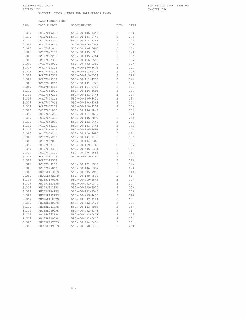
TM11-6625-3135-24P PCN X43CXXC084R PAGE 60SECTION IV TM-CODE FS6
NATIONAL STOCK NUMBER AND PART NUMBER INDEX
PART NUMBER INDEXFSCM PART NUMBER STOCK NUMBER FIG. ITEM
81349 RCR07G152JS 5905-00-106-1356 2 14381349 RCR07G181JS 5905-00-141-0742 2 20381349 RCR07G182GS 5905-00-114-5343 2 10381349 RCR07G184JS 5905-00-114-5344 2 23381349 RCR07G220JS 5905-00-106-3668 2 16481349 RCR07G221JS 5905-00-135-3973 2 12381349 RCR07G222JS 5905-00-105-7764 2 19781349 RCR07G223JS 5905-00-116-8556 2 13681349 RCR07G240JS 5905-00-442-9356 2 16981349 RCR07G242JS 5905-00-136-8406 2 10281349 RCR07G272JS 5905-00-111-4727 2 15681349 RCR07G273JS 5905-00-119-3504 2 12881349 RCR07G301JS 5905-00-111-4750 2 19481349 RCR07G302JS 5905-00-131-9729 2 10881349 RCR07G331JS 5905-00-114-0710 2 16181349 RCR07G360JS 5905-00-126-6698 2 12481349 RCR07G392JS 5905-00-141-0743 2 19381349 RCR07G432JS 5905-00-136-8431 2 19881349 RCR07G470JS 5905-00-104-8368 2 14481349 RCR07G471JS 5905-00-120-9154 2 10981349 RCR07G510JS 5905-00-106-1249 2 10481349 RCR07G512JS 5905-00-111-1679 2 17381349 RCR07G513JS 5905-00-136-3890 2 23281349 RCR07G560JS 5905-00-133-0440 2 22481349 RCR07G562JS 5905-00-141-0744 2 17281349 RCR07G620JS 5905-00-126-6692 2 14281349 RCR07G682JS 5905-00-110-7622 2 22181349 RCR07G752JS 5905-00-141-1132 2 13781349 RCR07G820JS 5905-00-104-8363 2 10181349 RCR07G821JS 5905-00-119-8768 2 12581349 RCR07G823JS 5905-00-435-6374 2 18181349 RCR07G911JS 5905-00-485-4554 2 11181349 RCR07G912JS 5905-00-115-2261 2 20781349 RCR32G103JS 2 17981349 RC707G391JS 5905-00-121-9932 2 19681349 RC707G750JS 5905-00-106-9357 2 22381349 RNC55H1130FS 5905-00-305-7959 2 11981349 RNC55H4020FS 5905-00-138-7530 2 9481349 RNC55J1000FS 5905-00-419-2845 2 14781349 RNC55J1432FS 5905-00-432-0370 2 24781349 RNC55J2212FS 5905-00-289-3920 2 20081349 RNC55J2942FS 5905-00-242-2546 2 15381349 RNC55K1021FS 5905-00-259-4433 2 14681349 RNC55K1100FS 5905-00-307-4104 2 9581349 RNC55K2002FS 5905-00-432-0402 2 12181349 RNC55K2210FS 5905-00-163-7092 2 18781349 RNC55K2490FS 5905-00-432-6378 2 11781349 RNC55K2671FS 5905-00-432-0408 2 24681349 RNC55K2800FS 5905-00-432-0410 2 20481349 RNC55K2870FS 5905-00-254-2451 2 19181349 RNC55K3092FS 5905-00-258-5403 2 208
I-6

TM11-6625-3135-24P PCN X43CXXC084R PAGE 61SECTION IV TM-CODE FS6
NATIONAL STOCK NUMBER AND PART NUMBER INDEX
PART NUMBER INDEXFSCM PART NUMBER STOCK NUMBER FIG. ITEM
81349 RNC55K3400FS 5905-00-284-6076 2 15981349 RNC55K3480FS 5905-00-264-4330 2 15881349 RNC55K3570FS 5905-00-481-1330 2 23981349 RNC55K4123FS 5905-01-102-8712 2 16581349 RNC55K4320FS 5905-00-758-4802 2 21381349 RNC55K4870FS 5905-00-137-4277 2 11881349 RNC55K5361FS 5905-00-258-5882 2 21981349 RNC55K5760FS 5905-00-346-8062 2 14881349 RNC55K6040FS 5905-00-432-0425 2 12981349 RNC55K7150FS 5905-00-721-3736 2 14181349 RNC55K7320FS 5905-00-233-9202 2 19081349 RNC55K82R5FS 5905-00-452-0736 2 11381349 RNC60K1002FS 2 24081349 RNC60K1330FS 5905-00-428-3857 2 21281349 RNC60K1331FS 5905-00-721-2376 2 21581349 RNC60K1501FS 5905-00-758-4840 2 21181349 RNC60K1691FS 5905-00-112-7039 2 19281349 RNC60K1821FS 5905-00-426-7129 2 14981349 RNC60K2001FS 5905-00-138-1285 2 22581349 RNC60K4120FS 5905-00-506-6563 2 16081349 RNC60K6980FS 5905-00-192-3461 2 11281349 RNC60K7320FS 5905-01-013-3179 2 13281349 RNC60K75R0FS 5905-00-426-7144 2 18381349 RNC60K7680FS 5905-00-488-3277 2 18981349 RNC60K8452FS 5905-00-311-2351 2 24181349 RNR60C1581FS 5905-00-372-0039 2 15191637 RS1A-90-R2J 2 23796733 R3207 5910-01-187-6085 2 2604713 SJE389 2 9101295 SKA6664 5961-00-417-4107 2 7301295 SN74LS03 2 27301295 SN74LS09 2 27204713 SN74LS132NDS 2 27004713 SPS6700 5961-00-359-9493 2 8704713 SPS6866K 5961-00-946-6635 2 8104713 SPS6868 2 8004713 SPS8223 5961-01-192-0077 2 7004713 SPS8224 5961-01-192-1602 2 7904713 SPS8236 5961-00-189-1266 2 7404713 SPS8246 5961-01-128-2797 2 8204713 SPS8317 2 7604713 SPS8608M 2 7704713 SPS8802-1 5961-00-879-7450 2 8404713 SRF 518 5961-00-103-6748 2 7204713 SZG15RL 5961-00-548-1964 2 28204713 SZG20012 2 27804713 SZG30214RL 2 28004713 SZG35009K3 2 27704713 SZG35009K7 2 28404713 SZ11738RL 5961-00-936-7720 2 28304713 SZ13294RL 5961-01-005-9751 2 279
I-7

TM11-6625-3135-24P PCN X43CXXC084R PAGE 62SECTION IV TM-CODE FS6
NATIONAL STOCK NUMBER AND PART NUMBER INDEX
PART NUMBER INDEXFSCM PART NUMBER STOCK NUMBER FIG. ITEM
90201 TAC105K035P02 2 2814552 TD3810983 2 28101295 TL594CN 2 27557668 TR50J-E 120E 2 25357668 TR50J-E 4K7 2 24857668 TR50J-E 5K1 2 22257668 TR50J-E 510K 2 23457668 TR50J-E2K 2 24957668 TR50J-E82K 2 23627014 T07391E2 5961-01-078-3606 2 8551642 T150-050NP0180J 2 512969 UES1106 5961-01-188-6042 2 5555680 UHC2C330TFA 2 4755680 ULA1A220TEA 5910-01-062-7349 2 1855680 ULB1E101MEA 5910-01-185-9359 2 4455680 ULB1E102TFAANA 2 4512969 UTR307 5961-01-026-5373 2 5812969 UTR308 5961-00-896-6805 2 5790201 VPR271N040E1E1C 2 4890201 VPX841N012E1E1C 2 4954583 ZUB2203-00 1 5280009 010-6101-02 6625-00-463-5241 1 7380009 010-6101-03 6625-01-119-0155 1 7080009 010-6122-01 1 6480009 013-0107-04 1 6580009 015-0201-04 6625-01-112-5966 1 7480009 016-0566-00 5999-01-138-5897 1 759660 0301-080C0J0339C 2 5056289 1C20C0G332J100B 2 2304713 1N5817 5961-01-017-0390 2 5980009 108-0420-00 5950-00-472-0426 2 6680009 119-1515-00 1 3980009 119-1788-00 1 5080009 120-1347-00 2 25880009 120-1594-00 2 25978189 1224-02 5310-00-197-4505 1 5480009 129-0999-00 1 6180009 131-2844-00 1 6280009 136-0628-00 1 1880009 136-0830-00 2 29080009 151-0164-00 5961-00-931-8250 2 8980009 151-0276-00 5961-00-404-5537 2 8380009 151-0347-00 5961-00-365-9935 2 8680009 151-0443-00 5961-01-127-8397 2 8880009 152-0141-02 5961-00-105-7681 2 5180009 154-0861-00 1 1180009 155-0274-00 2 26060935 158/.068/M/250/H 2 4056289 17D1149 2 4156289 173D225X0020V 2 856289 173D335X9015V 2 24
I-8

TM11-6625-3135-24P PCN X43CXXC084R PAGE 63SECTION IV TM-CODE FS6
NATIONAL STOCK NUMBER AND PART NUMBER INDEX
PART NUMBER INDEXFSCM PART NUMBER STOCK NUMBER FIG. ITEM
80009 175-0124-01 6625-00-563-0090 1 7180009 175-0125-01 6625-01-016-8693 1 7280009 175-1661-01 6625-01-139-3375 1 7580009 175-2546-01 2 30580009 175-3217-00 1 6880009 175-6136-00 2 30280009 175-6137-00 2 30180009 175-6138-00 2 30480009 175-6139-00 2 29380009 175-6140-00 1 1980009 175-6141-00 2 30680009 195-0389-00 1 5180009 195-1870-00 1 6680009 195-5499-00 1 5380009 195-6176-00 1 6780009 195-7063-00 2 28880009 195-7064-00 2 28780009 195-7065-00 2 8680009 195-8235-00 2 28980009 198-4819-00 2 30356289 2C20Z5U104Z200B 2 3650157 2D1595 5905-01-034-0704 2 25480131 2N3904 5961-00-892-8706 2 7173743 2X-20319-402 5310-00-231-4954 1 1780009 200-1388-03 1 5580009 200-2264-00 5920-01-126-8941 1 4980009 200-2519-00 1 4080009 200-2520-00 1 180009 200-2538-00 1 380009 200-2735-00 2 29120932 202EL200AT222K 5910-00-237-1196 2 3480009 204-0833-00 5920-01-123-9854 1 4795712 2048-2NT34 1 7880009 206-0191-03 6625-01-039-3503 1 7778189 211-041800-00 5310-00-836-3520 1 41
2 29980009 214-3375-00 1 3719396 223K02PT485 2 3501121 23M909 2 23514752 230B1E105K 2 4280009 234-0107-20 2 26580031 2502A0R503VP02F0 5910-01-062-7224 2 3334899 2743001111 2 6224931 28P224-1 6625-01-112-5250 1 7680009 281-0140-// 5910-00-456-9019 2 780009 281-0500-00 5910-00-682-3287 2 980009 281-0768-00 5910-00-114-0805 2 1580009 281-0772-00 5910-01-062-1970 2 380009 281-0775-00 5910-01-062-1968 2 1780009 283-0481-00 2 4359660 301-000C0G0220K 5910-00-903-8336 2 12
I-9

TM11-6625-3135-24P PCN X43CXXC084R PAGE 64SECTION IV TM-CODE FS6
NATIONAL STOCK NUMBER AND PART NUMBER INDEX
PART NUMBER INDEXFSCM PART NUMBER STOCK NUMBER FIG. ITEM
80009 308-0441-00 5905-00-247-2970 2 24580009 308-0677-00 2 25013511 31-279 5935-00-001-7558 1 4680009 311-1183-02 1 2580009 311-2177-02 1 2080009 315-0332-00 2 20280009 315-0621-00 2 13880009 321-0203-00 2 15480009 321-0209-00 5905-00-431-7827 2 21780009 321-0223-0 5905-00-426-7708 2 9780009 321-0228-00 2 22680009 321-0274-00 5905-01-091-5481 2 15580009 333-3109-00 1 2780009 334-2363-00 2 29232997 3352T-CK5-501 5905-01-034-3413 2 14532997 3352T-1-102 5905-01-113-2859 2 20532997 3352T-1-104 5905-01-077-9702 2 23132997 3352T-1-203 5905-01-077-9708 2 22932997 3352T-1-251 5905-01-036-6416 2 21095712 33600-1 5935-00-832-4946 1 6980009 337-2775-01 1 1032997 3386X-T07-102 5905-00-560-3132 2 12780009 342-0555-00 2 29780009 342-0582-00 2 29480009 343-0969-00 2 29680009 343-1025-00 2 29580009 344-0132-00 5340-00-479-4346 1 4380009 344-0347-00 1 4580009 348-0555-00 1 4480009 348-0659-01 1 580009 358-0550-00 1 2680009 361-1047-00 2 30080009 366-1031-03 5355-00-492-2316 1 3380009 366-1146-00 5355-00-419-4032 1 1680009 366-1391-03 1 1280009 366-1480-03 1 3480009 366-1840-03 1 3080009 366-1850-00 1 2980009 366-2013-00 1 5980009 366-2049-01 1 1580009 366-2052-01 1 3180009 366-2146-03 1 1480009 366-2148-01 1 3280009 367-0289-00 1 480009 377-0512-00 1 3680009 378-0237-00 1 980009 384-1575-00 1 3580009 384-1576-01 1 2180009 390-0790-11 1 280009 407-2729-00 2 29880009 426-1765-02 1 8
I-10

TM11-6625-3135-24P PCN X43CXXC084R PAGE 65SECTION IV TM-CODE FS6
NATIONAL STOCK NUMBER AND PART NUMBER INDEX
PART NUMBER INDEXFSCM PART NUMBER STOCK NUMBER FIG. ITEM
56289 430P582 2 3905129 461-S-70 5355-01-005-4089 1 2822526 48283-029 5999-00-275-0213 2 6922526 48283-036 5940-01-159-2407 2 6800779 5-3809509 2 6504222 5R305SE474MAA 2 2154937 5002573 2 25780031 5043CX10K00J 5905-01-132-1353 2 12219701 5043CX510K0J 2 24202114 56-590-65/4A6 5950-00-443-9512 2 6380009 670-7615-00 1 4280009 670-8404-00 6625-01-197-1938 1 5680009 670-8405-00 1 5780009 670-8406-00 1 5880009 670-8407-00 1 2380009 670-8418-00 1 1380009 670-8444-00 1 6080009 670-8819-00 1 2480009 672-0111-00 1 3873138 72-23-0 5905-01-013-1415 2 12673138 72-27-0 5905-00-556-2944 2 11007263 74LS74A 2 27159660 805534Y5D0152J 2 459660 855-XXXY5E0222J 5910-00-465-9742 2 3259660 878521SY5S102M 2 3807263 96LS02 2 26777820 9663-1 NT-34 5935-01-147-3771 1 63
I-11