Embed Size (px)
Citation preview

Technical Manual CC121ARCNET Interface for VMEbusVersion 2.0 March 1992
Chapter 1 General Information
1.1 Introduction
This manual provides general information, preparation for use, installation instructions and theory ofoperation for the CC121 module. The manual includes basic information needed by software engineersto design and implement software for the module.
1.2 Features
The features of the CC121 module include:
VMEbus Interface
• Double Eurocard form factor
• 7-level interrupt requester with software programmable vector
• Register to mask interrupts or reset ARCNET controller
• 2-kbyte fast dual ported RAM for data packets
• Occupies 4 kbyte of memory in the short or standard address space
• Supervisory mode only, or both supervisory and non-privileged access modes can be selected
Local Area Network
• ARCNET interface for coax or twisted-pair
• Interface signals on front-panel connector and P2
• Uses SMC COM9026 protocol controller
• Selectable high-, or low-impedance coax interface
• Onboard register to read node ID
1.3 General Description
The CC121 ARCNET interface is a VMEbus module that allows to interface VMEbus systems to ARC-NET token-passing networks. The board, which is based on the SMC COM9026 ARCNET controller,includes a 2-kbyte high-speed dual-ported RAM data buffer. It operates as a VMEbus slave module with8-bit access to the controller chip and onboard registers, and 8- or 16-bit access to the data buffer. Aseparate control register allows the user to mask interrupts from the controller, or reset the board.Another register allows the user to read the ARCNET node ID at any time.
Technical Manual Page 1-1 Compcontrol
General Information CC121
1.4 Related Documents
The following documentation can be referred to for detailed information about related items notdescribed in this manual.
Table 1-1 List of Documents
Doucment Title Published by
COM9026 Local Area Network Controller SMC
IDT7130 CMOS Dual Port RAM (1Kx8) IDT
ARCNET Cabling Guide (doc nr 51087, ed 2) Datapoint
ARCNET Local Area Network Standard Arcnet Trade Association
HYC9088 Twisted Pair or Coax Medium Transceiver SMC
Compcontrol Page 1-2 Technical Manual
Chapter 2 Specifications
2.1 Introduction
The CC121 is a network interface module for ARCNET. The module uses a 20-MHz COM9026 protocolcontroller, and the COM9032 network transceiver. The on-board medium interface is a high-, or low-impedance coax interface or a twisted-pair interface. The coax interface uses a BNC connector at thefront panel. The transceiver signals for a twisted-pair interface are available at the VMEbus P2 connec-tor. A twisted-pair interface typically uses an RJ11 connector.
The following section gives an overview of the main parts that are used on the CC121 module.
2.2 Components Used
The local memory consists of two high-speed dual-port RAM devices, that can be accessed by theonboard protocol controller and by a VMEbus master. The memory has a capacity of 2 kbytes, which isused to buffer up to four 512-byte data packets.
The COM9026 device provides the ARCNET network protocol handling. With its 2.5 Mbit/s data rate, upto 255 network nodes, and data packet sizes of up to 512 bytes, the ARCNET local area network is areliable (token passing), high performance, and low-cost network solution for real-time industrial appli-cations.
The HYC9088 is a hybrid module which interfaces the ARCNET local area network controller to tele-phone twisted pair, or coax cables.
2.3 General Specifications
Power Requirements
• 1.4 A Max (1.0 A Typ) at +5 VDC
• 240 mA Max (180 mA Typ) at -12 VDC
Physical Configuration Options
• Size: 160 mm x 233.35 mm x 20 mm
• Weight: 330 gram
Environmental Requirements
• Operating temperature: 0 to 70 degrees C
• Max operating humidity: 90%
Technical Manual Page 2-1 Compcontrol
Specifications CC121
2.4 VMEbus Specifications
Data Transfer Options
• A24,A16/D16,D8 RMW slave
• DPR read access: 120 ns (typ)DPR write access: 120 ns (typ)
• DPR cycle time: 150 ns (typ)
Interrupt Options
• D08(O)/I(1,2,3,4,5,6,7) static
• Programmable vector
• ROAK interrupter
2.5 Network Specifications
Network Interface Options
• 2.5 Mbit/s ARCNET interface
• Coax medium interface: RG62A/U cable
• Onboard termination (jumper selectable)
• Onboard BNC connector
• Twisted-pair medium interface: RS-485
• Off-board RJ11 connector
Compcontrol Page 2-2 Technical Manual
Chapter 3 Functional Description
3.1 Introduction
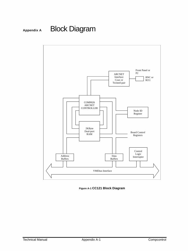
This chapter gives an overview of the CC121 module, and a detailed description of the functional sec-tions. The block diagram of the module is given in Appendix A
Signal names that are used in the schematic diagrams, have a horizontal bar (-)or end with an asterisk(*), when the signal is active low.
3.2 VMEbus Interface
The VMEbus interface is used by to access resources on the CC121 module. These resources includea 2-kbyte dual-port data buffer, the ARCNET protocol controller, and some general control registers.The data buffer is used to hold data packets temporarily prior to transmission on the network and as atemporary storage of all received data packets directed to this particular node. The processor writescommands to the protocol controller and can read its status. The onboard control registers are used toread the ARCNET node ID, and to control the interrupt function of the board.
The CC121 occupies 4-kbytes in the VMEbus standard, or short I/O address space. The address selec-tion is made with hexadecimal switches, and the address modifiers are selected with jumpers. Theinterrupt level is also selected with jumpers, and the interrupt vector is software programmable.
3.3 ARCNET Interface
The COM9026 is used to implement the ARCNET interface. This device has a microprocessor interfacewith low-overhead software requirements. It establishes the network configuration, and automaticallyre-configures the network as new nodes are added or deleted from the network. The 8-position DIPswitch on the CC121 module is used to select the ARCNET node ID.
The CC121 module supports three ARCNET medium interfaces, that all have specific advantages fordifferent environments. The RG-58 coax cable is the most often used medium, and uses a standardBNC connector on the front panel. Onboard cable termination has been implemented and can beselected with a jumper.
The lowest cost network medium is a telephone twisted pair cable, and uses the P2 connector for con-nection to the network.
Dual-Port Memory
The data buffer, used by both the microprocessor and protocol controller to transfer data packets, hasbeen implemented as a dual-port RAM. This memory configuration dramatically improves the memory
Technical Manual Page 3-1 Compcontrol

Functional Description CC121
access time, because the VMEbus master can transfer data packets to/from this memory using high-speed 16-bit transfers.
Compcontrol Page 3-2 Technical Manual

Chapter 4 Installation Procedure
4.1 Introduction
This chapter provides the preparation and installation instructions for the CC121 ARCNET interfacemodule.
4.2 Installation
The module is shipped in an anti-static container which protects it against static electricity. When themodule is unpacked, avoid touching areas of integrated circuitry to prevent static discharge from dam-aging the circuits.
Before the module can be used, several on-board switches and jumpers must be checked for propersettings. Jumpers are used to select hardware specific options.
NOTE: ENSURE THAT POWER IS TURNED OFF BEFOREINSERTING OR WITHDRAWING THE CC121 MODULE IN ORFROM THE SYSTEM BACKPLANE.
4.3 Jumper Settings
All jumper settings discussed in the following sections are illustrated as seen from the component sidewith the VMEbus connectors downwards. The next table gives a summary of the default jumper andswitch settings and their function.
Technical Manual Page 4-1 Compcontrol
Installation Procedure CC121
4.3.1 Network Time Out Selection
There are three time-outs associated with the COM9026 operation. These time-outs are referred to asResponse Time, Idle Time, and Reconfiguration Time. The ARCNET protocol relies on a token passingscheme. If any node does not receive the token within the Reconfiguration Time, the node will initiate aNetwork Reconfiguration.
Two jumper blocks have been provided to increase the time-out periods, which allow the network tooperate over longer distances than 4 miles.
Table 4-1 Jumper Setting
Description JumperBlock
DefaultSetting
Status Section
Network Time Out JB1 Not Connected Max. 4 miles 4.3.1
Cable Ground JB2 1-2 Connected VMEbus GND 4.3.2
IRQ Level JB3 5-6 Connected Level 3 4.3.3
Access Mode JB4 Not Connected Both sup. and n.p. 4.3.4
Addressing Mode JB5 2-3 Connected Short addressing 4.3.4
Coax Termination JB6 Not Connected High Impedance 4.3.5
Node ID SW1 Switch 5 ON, rest OFF Node ID $10 4.3.6
Address (A15-A12) SW2 ’D’ Address $D000 4.3.4
Address (A19-A16) SW3 ’F’ Don’t care 4.3.4
Address (A23-A20) SW4 ’F’ Don’t Care 4.3.4
Table 4-2 Time Out Values
JB1ResponseTime
IdleTime
ReconfigurationTime
78 µs 86 µs 840 ms
285 µs 316 µs 1680 ms
563 µs 624 µs 1680 ms
1130 µs 1237 µs 1680 ms
Compcontrol Page 4-2 Technical Manual
CC121 Installation Procedure
The default time-out setting for a typical ARCNET network requires no jumpers at JB1.
For proper working of the ARCNET protocol, it is necessary that all nodes connected to the networkuse the same time-out periods.
4.3.2 Cable Ground Decoupling
The signal lines of the ARCNET medium for twisted pair and coax are decoupled with an RC network.The user can select with JB2 whether the decoupling is to VMEbus GND or to Chassis GND. If “chassisGND” is selected, a proper chassis GND connection must exist at pin 3 of row C of the P2 connector.
Figure 4-1 Cable Ground Decoupling
4.3.3 VMEbus Interrupt Level
JB3 allows the user to select the interrupt level that is generated on the VMEbus. JB3 is decoded as a3-bit binary input. A jumper installed represents a “0”. No jumper installed represents a “1”. When level0 is selected (i.e. all jumpers installed), the interrupt function will be disabled. The figure on the nextpage shows the possible jumper settings and their status.
1
2
JB2
Cable ground decoupled toVMEbus GND
1
2
JB2
Cable ground decoupled toChassis GND(Pin 3 at the P2 connector)
Technical Manual Page 4-3 Compcontrol
Installation Procedure CC121
Figure 4-2 Interrupt Level Selection
4.3.4 VMEbus Address Selection
To access resources on the CC121, the VMEbus master may use standard or short addressing, andsupervisory and/or non-privileged access. Two jumpers and three hex switches are used to select theaddress mode and address of the CC121 module.
Figure 4-3 CC121 Access Mode
1
3
5
2
4
6
1
3
5
2
4
6
1
3
5
2
4
6
1
3
5
2
4
6
JB3JB3 JB3 JB3
IRQ Level:Disabled
IRQ Level:1
IRQ Level:3
1
3
5
2
4
6
1
3
5
2
4
6
1
3
5
2
4
6
1
3
5
2
4
6
JB3 JB3 JB3 JB3
IRQ Level:5
IRQ Level:6
IRQ Level:7
IRQ Level:4
IRQ Level:2
CC121 responds at bothsupervisory and non-privilegedaccess
CC121 responds at supervisoryaccess only
1
2
JB4
1
2
JB4
Compcontrol Page 4-4 Technical Manual
CC121 Installation Procedure
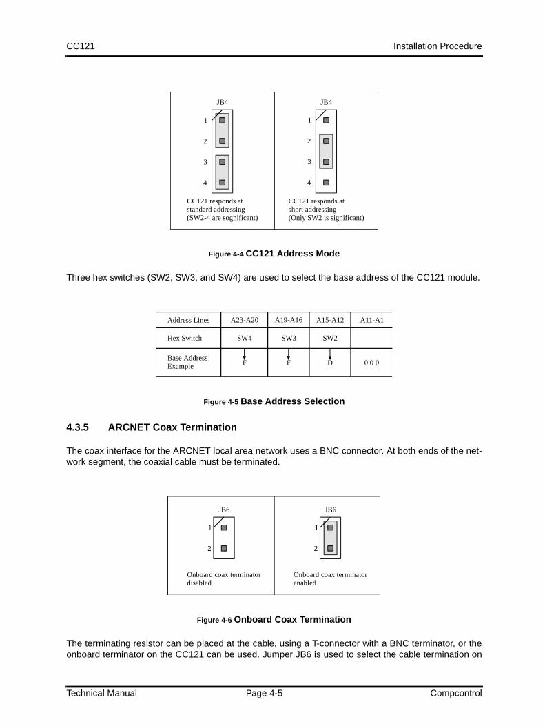
Figure 4-4 CC121 Address Mode
Three hex switches (SW2, SW3, and SW4) are used to select the base address of the CC121 module.
Figure 4-5 Base Address Selection
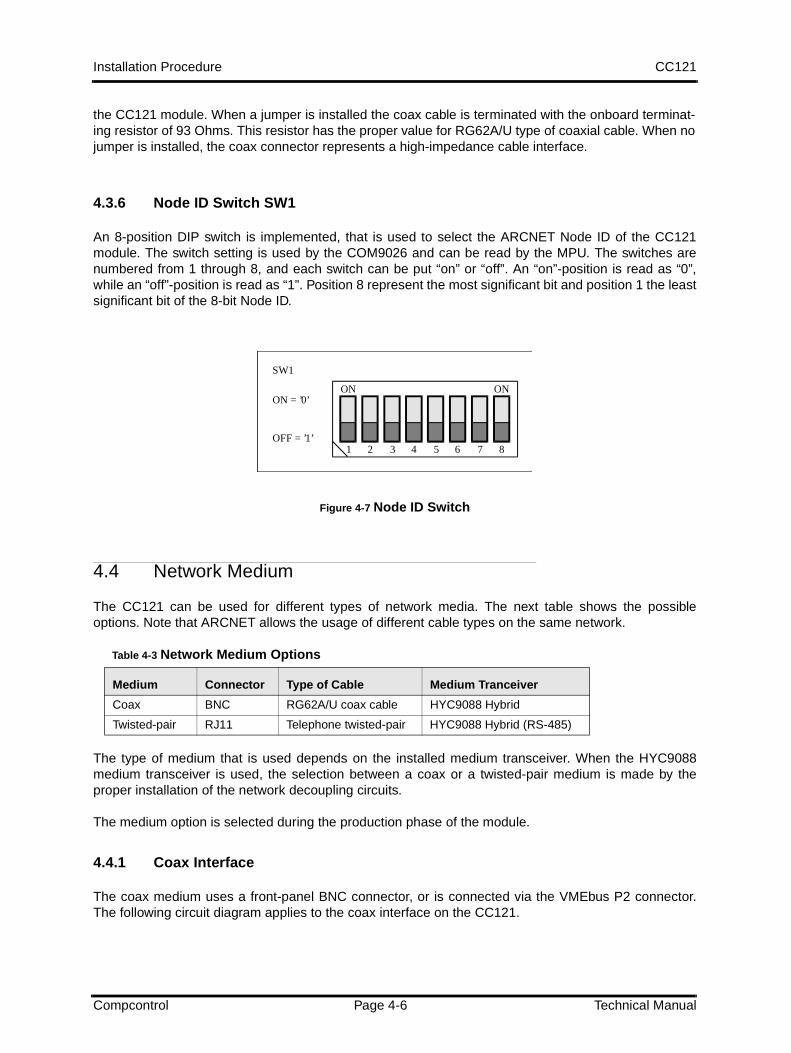
4.3.5 ARCNET Coax Termination
The coax interface for the ARCNET local area network uses a BNC connector. At both ends of the net-work segment, the coaxial cable must be terminated.
Figure 4-6 Onboard Coax Termination
The terminating resistor can be placed at the cable, using a T-connector with a BNC terminator, or theonboard terminator on the CC121 can be used. Jumper JB6 is used to select the cable termination on
1
2
3
4
1
2
3
4
JB4 JB4
CC121 responds atstandard addressing(SW2-4 are sognificant)
CC121 responds atshort addressing(Only SW2 is significant)
Address Lines A23-A20 A19-A16 A15-A12 A11-A1
Hex Switch SW4 SW3 SW2
Base AddressExample F F D 0 0 0
1
2
1
2
JB6 JB6
Onboard coax terminatordisabled
Onboard coax terminatorenabled
Technical Manual Page 4-5 Compcontrol
Installation Procedure CC121
the CC121 module. When a jumper is installed the coax cable is terminated with the onboard terminat-ing resistor of 93 Ohms. This resistor has the proper value for RG62A/U type of coaxial cable. When nojumper is installed, the coax connector represents a high-impedance cable interface.
4.3.6 Node ID Switch SW1
An 8-position DIP switch is implemented, that is used to select the ARCNET Node ID of the CC121module. The switch setting is used by the COM9026 and can be read by the MPU. The switches arenumbered from 1 through 8, and each switch can be put “on” or “off”. An “on”-position is read as “0”,while an “off”-position is read as “1”. Position 8 represent the most significant bit and position 1 the leastsignificant bit of the 8-bit Node ID.
Figure 4-7 Node ID Switch
4.4 Network Medium
The CC121 can be used for different types of network media. The next table shows the possibleoptions. Note that ARCNET allows the usage of different cable types on the same network.
The type of medium that is used depends on the installed medium transceiver. When the HYC9088medium transceiver is used, the selection between a coax or a twisted-pair medium is made by theproper installation of the network decoupling circuits.
The medium option is selected during the production phase of the module.
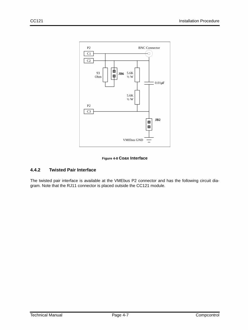
4.4.1 Coax Interface
The coax medium uses a front-panel BNC connector, or is connected via the VMEbus P2 connector.The following circuit diagram applies to the coax interface on the CC121.
Table 4-3 Network Medium Options
Medium Connector Type of Cable Medium Tranceiver
Coax BNC RG62A/U coax cable HYC9088 Hybrid
Twisted-pair RJ11 Telephone twisted-pair HYC9088 Hybrid (RS-485)
1 2 3 4 5 6 7 8
ON ONON = ’0’
OFF = ’1’
SW1
Compcontrol Page 4-6 Technical Manual
CC121 Installation Procedure
Figure 4-8 Coax Interface
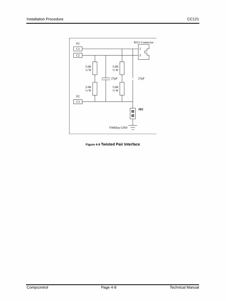
4.4.2 Twisted Pair Interface
The twisted pair interface is available at the VMEbus P2 connector and has the following circuit dia-gram. Note that the RJ11 connector is placed outside the CC121 module.
C1
C2
C3
P2
P2 BNC Connector
93Ohm
JB6 5.6K½ W
5.6K½ W
0.01 Fµ
JB2
VMEbus GND
Technical Manual Page 4-7 Compcontrol
Installation Procedure CC121
Figure 4-9 Twisted Pair Interface
C1
C2
C3
P2
P2
5.6K½ W
5.6K½ W
5.6K½ W
5.6K½ W
27pF27pF
JB2
VMEbus GND
2
3
RJ11 Connector
Compcontrol Page 4-8 Technical Manual
Chapter 5 Programming Considerations
5.1 Introduction
This section contains all necessary information for system programmers to take full advantage of thefeatures of the CC121 module. The descriptions will include implementation dependent information thatcannot be found in the respective data sheets. This chapter should be used in conjunction with the ref-erences given in paragraph 1.4.
System programmers are expected to be fully conversant with all the material mentioned in paragraph1.4 and have the relevant experience, when they want to write their own system software.
In Appendix C, the Memory map of the CC121 module is given. It also shows the register map of theperipherals.
5.2 Reset
When power is applied to the CC121 module, or the VMEbus SYSRESET* signal is activated, theonboard devices will be reset. These devices include the COM9026, the COM9032, and the board con-trol register. After reset the ARCNET protocol controller will perform an internal initialization cycle, andreads its node ID from the Node ID switch. The COM9026 will also generate a reset interrupt. Note thatthis interrupt will not immediately generate a VMEbus interrupt, because the interrupt enable bit of theboard control register is cleared during reset.
After successful initialization, the COM9026 will execute two write cycles to the dual-port RAM. Loca-tion 00 will be written with D1 (hex), and location 1 will be written with the Node ID value, as it was readfrom the Node ID switch. Only when the VMEbus master reads these patterns from the dual-port RAM,proper operation of the COM9026 is assured.
5.3 CC121 Memory Map
The local memory map takes a total of 4 kbytes in the VMEbus standard or short address space. It hasbeen divided in two 2-kbyte segments, where the first part is used to access the dual-port data buffer,and the second part the 8-bit devices.
The total memory map is shown in the next table. Note that address spaces marked with (*), arerepeated a number of times in the memory map. The number of times depends on the space that theperipheral occupies in the memory map. The size indication shows the allowed data transfer width.
Technical Manual Page 5-1 Compcontrol
Programming Considerations CC121
Note that only the 2-kbyte data buffer can be accessed for 16-bit transfers. The other peripherals mustbe accessed for 8-bit transfers and addressed at odd memory locations.
The next sections describe the devices in the memory map in more detail.
5.3.1 Dual-port Data Buffer
The data buffer is used to hold data packets temporarily prior to transmission on the network and as atemporary storage of all received data packets directed to the particular node. The 2-kbyte RAM bufferallows both transmit and receive operations to be double buffered with respect to the processor (VME-bus master). For instance, after one data packet has been loaded into a particular page within the databuffer and a transmit command for that page has been issued, the processor can start loading anotherpage with the next message. Similarly, after one message is received and completely loaded into onepage of the RAM buffer by the COM9026, another receive command can be issued to allow reception ofthe next packet while the first packet is read by the processor.
5.3.2 COM9026 ARCNET Interface
The COM9026 Local Area Network Controller (LANC) has been implemented to provide the ARCNETnetwork interface. The chip contains an internal microsequencer which performs all of the control oper-ations necessary to carry out the ARCNET protocol. The COM9026 contains a ’write interrupt mask’register, a ’read status’ register, and a ’write command’ register. The MPU controls the COM9026 viasoftware, by accessing the various registers. These actions are described in the data sheet. The nextfigure shows the registers of the protocol controller.
Table 5-1 CC121 Memory Map
Address Device Size
xxx000xxx7FF
Dual-port Data Buffer2Kbyte
8, 16 bit
xxx800xxx9FF
COM9026 (*)2 bytes
8 bit
xxxA00xxxBFF
Interrupt Vector Register (*)1 byte
8 bit
xxxC00xxxDFF
Board Control Register (*)1 byte
8 bit
xxxE00xxxFFF
Node ID Switch Register (*)1 byte
8 bit
Compcontrol Page 5-2 Technical Manual
CC121 Programming Considerations
Figure 5-1 COM9026 Registers
RI Receive Inhibit - This bit, if set high, indicates that a packet has been deposited into theRAM buffer page nn as specified by the last ENABLE RECEIVE TO PAGE nn com-mand. The setting of this bit can cause an interrupt if the corresponding mask bit in theinterrupt mask register and the interrupt enable bit in the board control register havebeen properly setup.No messages will be received until an ENABLE RECEIVE TO PAGE nn command isissued. After any message is received, the receiver is automatically inhibited by settingthis bit to a logic one.
ETS2 Extended Time Out Status 2 - This bit reflects the current logic value of the ETS2 inputpin, as determined by JB1.
ETS1 Extended Time Out Status 1 - This bit reflects the current logic value of the ETS2 inputpin, as determined by JB1.
POR Power On Reset - This bit, if set high, indicates that the COM9026 has been reset. Thesetting of this bit will cause an interrupt, if the enable interrupt bit of the board controlregister has been set. This bit is cleared by writing the CLEAR FLAGS command to thecommand register.
TEST Test - This bit is intended for test and diagnostic purposes. It will be a logic zero underany normal operating conditions.
RECON Reconfiguration - This bit, if set high, indicates that the reconfiguration timer has timedout because the RX input was idle for 78.2 µs (typ). The setting of this bit can cause aninterrupt if the corresponding mask bit in the interrupt mask register and the interrupt en-able bit in the board control register have been properly setup.The bit is reset low during a CLEAR FLAGS command.
TMA Transmit Message Acknowledge - This bit, if set high, indicates that the packet trans-mitted as a result of an ENABLE TRANSMIT FROM PAGE nn command has been pos-itively acknowledged. This bit should only be considered valid after the TA bit is set.Broadcast messages are never acknowledged.
TA Transmit Available - This bit, if set high, indicates that the transmitter is available fortransmitting. This bit is set at the conclusion of an ENABLE TRANSMIT FROM PAGE
01234567
R R R R R R R R
Address
$xxx801
Read Status Register Register
RI ETS2 ETS2 POR TEST RECON TMA TA
W W W W W W W W
01234567Address
$xxx801
Write Interrupt Mask Register
RI RECON TA
W W W W W W W W
01234567Address
$xxx803
Write Command Register
Command Byte
Technical Manual Page 5-3 Compcontrol

Programming Considerations CC121
nn command or upon execution of a DISABLE TRANSMITTER command. The settingof this bit can cause an interrupt if the corresponding mask bit in the interrupt mask reg-ister and the interrupt enable bit in the board control register have been properly setup.
The valid command bytes that can be written to the command register are showed in the next table.
5.3.3 Interrupt Vector Register
The interrupt output of the COM9026 is connected to the selected interrupt line on the VMEbus. JB3 isused to select the interrupt level on the VMEbus. The interrupt vector provided during an interruptacknowledge cycle is software programmable by writing to the interrupt vector register.
Figure 5-2 Interrupt Vector Register
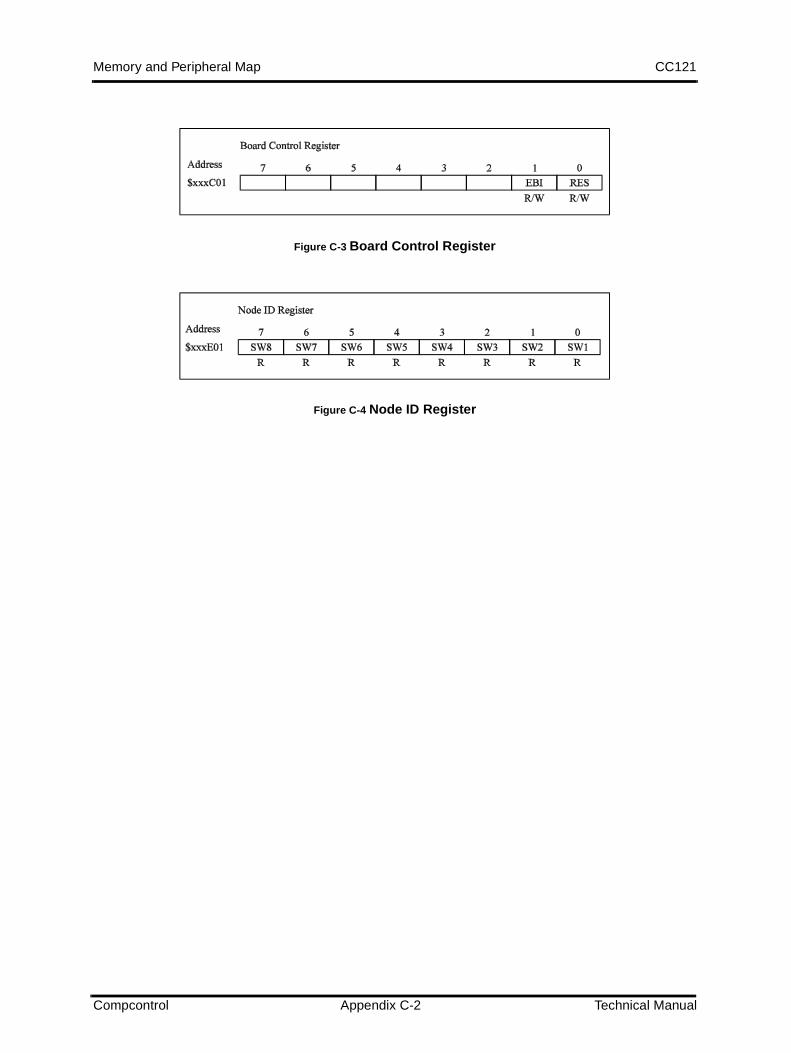
5.3.4 Board Control Registers
The board control register is used to generate a local reset to the CC121 board, and to control the inter-rupt output.
Figure 5-3 Board Control Register
Table 5-2 COM9026 Command Bytes
CommandByte
Description
0000 0000 RESERVED
0000 0001 DISABLE TRANSMITTER
0000 0010 DISABLE RECEIVER
000n n011 ENABLE TRANSMIT FROM PAGE nn
b00n n100 ENABLE RECEIVE TO PAGE nn(b determines if broadcast messages are to be received)
0000 c101 DEFINE CONFIGURATION
000r p110 CLEAR FLAGS (Reconfiguration and Power on)
R/W R/W R/W R/W R/W R/W R/W R/W
01234567Address
$xxxA01
Interrupt Vector Register
R/W R/W
01234567Address
$xxxC01
Board Control Register
EBI RES
Compcontrol Page 5-4 Technical Manual
CC121 Programming Considerations
EBI Enable Board Interrupt - If this bit is set, the interrupt output to the VMEbus is enabled.After reset this bit is cleared, which disables the interrupt output.
RES Reset - This bit is used to reset the COM9026 by writing a ’1’ followed by a ’0’. The timebetween the two consecutive write cycles determines the reset time and must be at least2 µs. This bit is cleared after a VMEbus reset.
5.3.5 Node ID Switch
An on-board DIP switch has been implemented, which setting can be read by the MPU at address$xxxE01. The register at $xxxE01 is read-only. The following figure shows the bit assignments of theregister.
Figure 5-4 Node ID Register
A switch that is in the ’on’ position will read as ’0’, and the ’off’ position will read as ’1’.
01234567
R R R R R R R R
Address
$xxxE01
Node ID Register
SW8 SW7 SW6 SW5 SW4 SW3 SW2 SW1
Technical Manual Page 5-5 Compcontrol

Programming Considerations CC121
Compcontrol Page 5-6 Technical Manual
Appendix A Block Diagram
Figure A-1 CC121 Block Diagram
AddressBuffers
DataBuffers
ControlLogic
Interrupter
COM9026ARCNET
CONTROLLER
2KByteDual-port
RAM
Node IDRegister
Board ControlRegisters
VMEbus Interface
ARCNETInterfaceCoax or
Twisted-pair
Front Panel orP2
BNC orRJ11
Technical Manual Appendix A-1 Compcontrol

Block Diagram CC121
Compcontrol Appendix A-2 Technical Manual

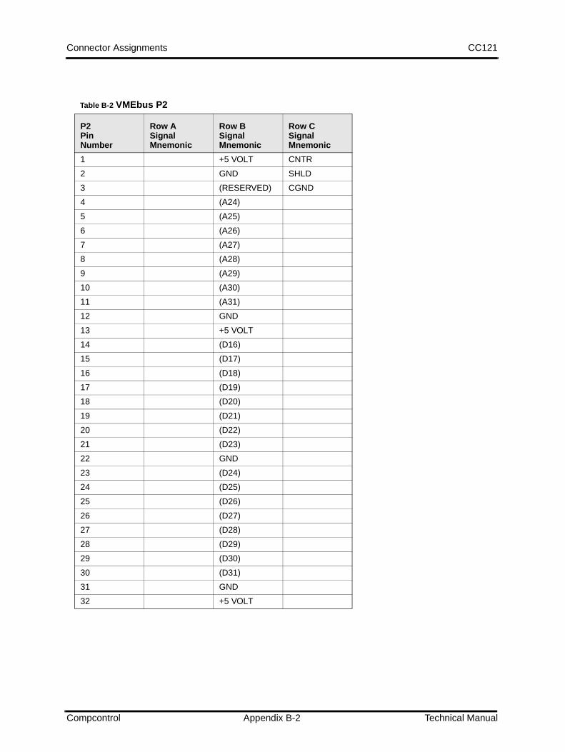
Appendix B Connector AssignmentsThis Appendix identifies the VMEbus connectors P1 and P2.
Note: Signal mnemonics that are shown in parenthesis are not used by the CC121 module.
Table B-1 VMEbus P1
Pin Number(a) SignalMnemonic
(b) SignalMnemonic
(c) SignalMnemonic
1 D00 (BBSY*) D08
2 D01 (BCLR*) D09
3 D02 (ACFAIL*) D10
4 D03 BG0IN* D11
5 D04 BG0OUT* D12
6 D05 BG1IN* D13
7 D06 BG1OUT* D14
8 D07 BG2IN* D15
9 GND BG2OUT* GND
10 (SYSCLK) BG3IN* (SYSFAIL*)
11 GND BG3OUT* BERR*
12 DS1* (BR0*) SYSRESET*
13 DS0* (BR1*) LWORD*
14 WRITE* (BR2*) AM5
15 GND (BR3*) A23
16 DTACK* AM0 A22
17 GND AM1 A21
18 AS* AM2 A20
19 GND AM3 A19
20 IACK* GND A18
21 IACKIN* (SERCLK) A17
22 IACKOUT* (SERDAT*) A16
23 AM4 GND A15
24 A07 IRQ7* A14
25 A06 IRQ6* A13
26 A05 IRQ5* A12
27 A04 IRQ4* A11
28 A03 IRQ3* A10
29 A02 IRQ2* A09
30 A01 IRQ1* A08
31 (-12V) (+5V STDBY) (+12V)
32 +5V +5V +5V
Technical Manual Appendix B-1 Compcontrol
Connector Assignments CC121
Table B-2 VMEbus P2
P2PinNumber
Row ASignalMnemonic
Row BSignalMnemonic
Row CSignalMnemonic
1 +5 VOLT CNTR
2 GND SHLD
3 (RESERVED) CGND
4 (A24)
5 (A25)
6 (A26)
7 (A27)
8 (A28)
9 (A29)
10 (A30)
11 (A31)
12 GND
13 +5 VOLT
14 (D16)
15 (D17)
16 (D18)
17 (D19)
18 (D20)
19 (D21)
20 (D22)
21 (D23)
22 GND
23 (D24)
24 (D25)
25 (D26)
26 (D27)
27 (D28)
28 (D29)
29 (D30)
30 (D31)
31 GND
32 +5 VOLT
Compcontrol Appendix B-2 Technical Manual

Appendix C Memory and Peripheral Map
Figure C-1 LANC (COM9026) Register Map
Figure C-2 Interrupt Vector Register
Table C-1 CC121 Memory Map
Address Device Size
xxx000xxx7FF
Dual-port Data Buffer2Kbyte
8, 16 bit
xxx800xxx9FF
COM9026 (*)2 bytes
8 bit
xxxA00xxxBFF
Interrupt Vector Register (*)1 byte
8 bit
xxxC00xxxDFF
Board Control Register (*)1 byte
8 bit
xxxE00xxxFFF
Node ID Switch Register (*)1 byte
8 bit
Technical Manual Appendix C-1 Compcontrol
Memory and Peripheral Map CC121
Figure C-3 Board Control Register
Figure C-4 Node ID Register
Compcontrol Appendix C-2 Technical Manual

Appendix D Photo CC121 Board
Figure D-1 Photo CC121 Board
Placeholder
Technical Manual Appendix D-1 Compcontrol

Photo CC121 Board CC121
Compcontrol Appendix D-2 Technical Manual