Embed Size (px)
Citation preview
Intel® Compute Module MFS2600KI
Technical Product Specification
Intel order number: G51989-002
Revision 1.0
June, 2012
Enterprise Platforms and Services Division

Revision History Intel® Compute Module MFS2600KI TPS
Revision 1.0
Intel order number: G51989-002
ii
Revision History
Date Revision
Number
Modifications
April, 2012 0.5 Initial release.
June, 2012 1.0 Corrected BMC LAN settings.
Disclaimers
Information in this document is provided in connection with Intel® products. No license, express or implied, by
estoppel or otherwise, to any intellectual property rights is granted by this document. Except as provided in Intel®’s
Terms and Conditions of Sale for such products, Intel® assumes no liability whatsoever, and Intel
® disclaims any
express or implied warranty, relating to sale and/or use of Intel® products including liability or warranties relating to
fitness for a particular purpose, merchantability, or infringement of any patent, copyright or other intellectual property right. Intel
® products are not intended for use in medical, lifesaving, or life sustaining applications. Intel
® may make
changes to specifications and product descriptions at any time, without notice.
Designers must not rely on the absence or characteristics of any features or instructions marked "reserved" or “undefined”. Intel
® reserves these for future definition and shall have no responsibility whatsoever for conflicts or
incompatibilities arising from future changes to them.
The Intel® Compute Module MFS2600KI may contain design defects or errors known as errata which may cause the
product to deviate from published specifications. Current characterized errata are available on request.
Intel Corporation server baseboards support peripheral components and contain a number of high-density VLSI and power delivery components that need adequate airflow to cool. Intel
®’s own chassis are designed and tested to meet
the intended thermal requirements of these components when the fully integrated system is used together. It is the responsibility of the system integrator that chooses not to use Intel
® developed server building blocks to consult
vendor datasheets and operating parameters to determine the amount of air flow required for their specific application and environmental conditions. Intel Corporation cannot be held responsible if components fail or the compute module does not operate correctly when used outside any of their published operating or non-operating limits.
Intel, Pentium, Itanium, and Xeon are trademarks or registered trademarks of Intel Corporation.
*Other brands and names may be claimed as the property of others.
Copyright © Intel Corporation 2012.
Intel® Compute Module MFS2600KI TPS Table of Contents
Revision 1.0 iii
Intel order number: G51989-002
Table of Contents
1. Introduction ........................................................................................................................ 1
1.1 Chapter Outline ...................................................................................................... 1
2. Product Overview ............................................................................................................... 2
2.1 Intel® Compute Module MFS2600KI Feature Set.................................................... 2
2.2 Compute Module Layout ........................................................................................ 3
2.2.1 Connector and Component Locations .................................................................... 3
2.2.2 External I/O Connector Locations ........................................................................... 4
3. Functional Architecture ..................................................................................................... 5
3.1 Intel® Xeon® processor ........................................................................................... 5
3.1.1 Processor Support ................................................................................................. 5
3.1.2 Processor Initialization Error Summary................................................................... 7
3.2 Processor Functions Overview ............................................................................... 9
3.2.1 Intel® QuickPath Interconnect ............................................................................... 10
3.2.2 Intel® Hyper-Threading Technology ...................................................................... 10
3.3 Processor Integrated I/O Module (IIO) .................................................................. 10
3.3.1 PCI Express Interfaces ......................................................................................... 10
3.3.2 DMI2 Interface to the PCH ................................................................................... 11
3.3.3 Integrated IOAPIC ................................................................................................ 11
3.3.4 Intel® QuickData Technology ................................................................................ 11
3.4 Memory Subsystem.............................................................................................. 11
3.4.1 Integrated Memory Controller (IMC) and Memory Subsystem .............................. 11
3.4.2 Publishing Compute Module Memory ................................................................... 15
3.4.3 Memory Map and Population Rules ...................................................................... 15
3.4.4 Memory RAS ........................................................................................................ 19
3.5 Intel® C602-J Chipset Overvew ............................................................................ 20
3.5.1 Digital Media Interface (DMI) ................................................................................ 21
3.5.2 PCI Express* Interface ......................................................................................... 21
3.5.3 Serial ATA (SATA) Controller ............................................................................... 21
3.5.4 Low Pin Count (LPC) Interface ............................................................................. 21
3.5.5 Serial Peripheral Interface (SPI) ........................................................................... 21
3.5.6 Advanced Programmable Interrupt Controller (APIC) ........................................... 21
3.5.7 Universal Serial Bus (USB) Controllers ................................................................ 22
3.6 Integrated Baseboard Management Controller Overview ..................................... 22
3.6.1 Super I/O Controller ............................................................................................. 22
3.6.2 Graphics Controller and Video Support ................................................................ 23
3.6.3 Baseboard Management Controller ...................................................................... 24
3.7 Network Interface Controller (NIC) ....................................................................... 25
3.8 Intel® Virtualization Technology for Directed I/O (Intel® VT-d) ............................... 26
Table of Contents Intel® Compute Module MFS2600KI TPS
Revision 1.0
Intel order number: G51989-002
iv
4. System Security ................................................................................................................ 27
4.1 BIOS Password Protection ................................................................................... 27
4.2 Trusted Platform Module (TPM) Support .............................................................. 28
4.2.1 TPM security BIOS ............................................................................................... 28
4.2.2 Physical Presence ................................................................................................ 29
4.2.3 TPM Security Setup Options ................................................................................ 29
4.3 Intel® Trusted Execution Technology .................................................................... 30
5. Connector/Header Locations and Pin-outs .................................................................... 31
5.1 Board Connector Information ............................................................................... 31
5.2 Power Connectors ................................................................................................ 31
5.3 I/O Connector Pin-out Definition ........................................................................... 32
5.3.1 VGA Connector .................................................................................................... 32
5.3.2 I/O Mezzanine Card Connector ............................................................................ 32
5.3.3 Midplane Signal Connector .................................................................................. 36
5.3.4 Serial Port Connector ........................................................................................... 37
5.3.5 USB 2.0 Connectors............................................................................................. 37
5.3.6 Low Profile eUSB SSD Support ........................................................................... 38
6. Jumper Block Settings ..................................................................................................... 39
6.1 CMOS Clear and Password Clear Usage Procedure ............................................ 40
6.2 Integrated BMC Force Update Procedure ............................................................ 41
6.3 Integrated BMC Initialization ................................................................................. 41
6.4 ME Force Update Jumper .................................................................................... 41
6.5 BIOS Recovery Jumper ........................................................................................ 42
7. Product Regulatory Requirements .................................................................................. 43
7.1 Product Regulatory Requirements ........................................................................ 43
7.2 Product Regulatory Compliance and Safety Markings .......................................... 43
7.3 Product Environmental/Ecology Requirements ..................................................... 43
Appendix A: Integration and Usage Tips .............................................................................. 44
Appendix B: POST Code Diagnostic LED Decoder .............................................................. 45
Appendix C: POST Error Code ............................................................................................... 50
Appendix D: Supported Intel® Modular Server System ........................................................ 56
Glossary .................................................................................................................................. 57
Reference Documents ............................................................................................................ 60
Intel® Compute Module MFS2600KI TPS List of Figures
Revision 1.0 v
Intel order number: G51989-002
List of Figures
Figure 1. Component and Connector Location Diagram .............................................................. 3
Figure 2. Intel® Compute Module MFS2600KI Front Panel Layout .............................................. 4
Figure 3. Intel® Compute Module MFS2600KI Functional Block Diagram .................................... 5
Figure 4. Processor Socket Assembly ......................................................................................... 6
Figure 5. Intergrated Memory Controller (IMC) and Memory Subsystem ................................... 11
Figure 6. DIMM Slot Order ........................................................................................................ 18
Figure 7. Integrated BMC Functional Block Diagram ................................................................. 22
Figure 8. eUSB SSD Support .................................................................................................... 38
Figure 9. Recovery Jumper Blocks ............................................................................................ 39
Figure 10. POST Code Diagnostic LED Decoder ...................................................................... 45
Figure 11. Intel® Modular Server System MFSYS25V2 ............................................................. 56
List of Tables Intel® Compute Module MFS2600KI TPS
Revision 1.0
Intel order number: G51989-002
vi
List of Tables
Table 1. Intel® compute module MFS2600KI Feature Set ........................................................... 2
Table 2. Mixed Processor Configurations .................................................................................... 8
Table 3. Intel® Compute Module MFS2600KI PCIe Bus Segment Characteristics ..................... 11
Table 4. UDIMM Support Guidelines (Preliminary. Subject to Change) ..................................... 13
Table 5. RDIMM Support Guidelines (Preliminary. Subject to Change) ..................................... 14
Table 6. LRDIMM Support Guidelines (Preliminary. Subject to Change) ................................... 14
Table 7. DDR3 RDIMM Population within a Channel................................................................. 16
Table 8. DDR3L Low Voltage RDIMM Population within a Channel .......................................... 16
Table 9. DDR3 UDIMM Population within a Channel................................................................. 17
Table 10. DDR3L Low Voltage UDIMM Poplulation within a Channel ....................................... 17
Table 11. Intel® Compute Module MFS2600KI DIMM Nomenclature ......................................... 18
Table 12. Video Modes ............................................................................................................. 23
Table 13. Video mode ............................................................................................................... 24
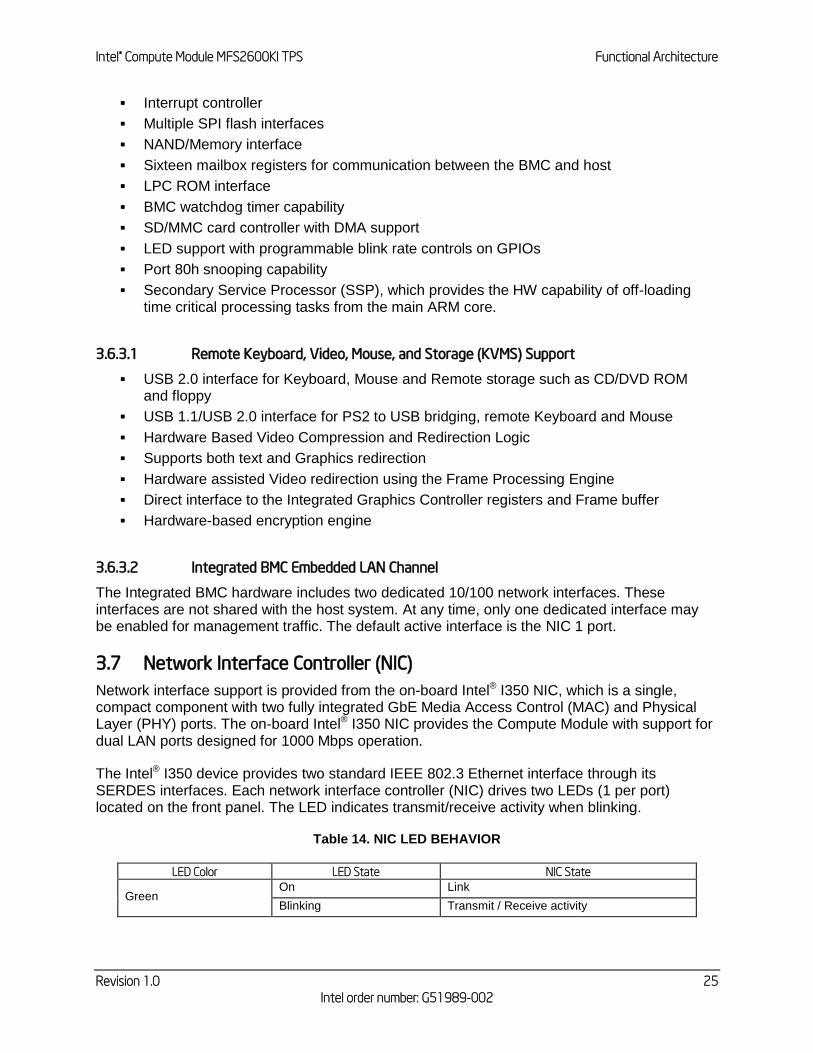
Table 14. NIC LED BEHAVIOR ................................................................................................. 25
Table 15. Board Connector Matrix............................................................................................. 31
Table 16. Power Connector Pin-out (J1A1) ............................................................................... 31
Table 17. VGA Connector Pin-out (J2K1) .................................................................................. 32
Table 18. 120-pin I/O Mezzanine Card Connector Pin-out ........................................................ 33
Table 19. 120-pin I/O Mezzanine Card Connector Signal Definitions ........................................ 34
Table 20. 40-pin I/O Mezzanine Card Connector Pin-out .......................................................... 36
Table 21. 96-pin Midplane Signal Connector Pin-out................................................................. 36
Table 22. Internal 9-pin Serial Header Pin-out (J4K1) ............................................................... 37
Table 23. External USB Connector Pin-out ............................................................................... 38
Table 24. Pin-out of Internal USB Connector for low-profile Solid State Drive (J1K1) ................ 38
Table 25. Recovery Jumpers .................................................................................................... 40
Table 26. POST Progress Code LED Example ......................................................................... 45
Table 27. POST Progress Codes .............................................................................................. 46
Table 28. MRC Progress Codes ............................................................................................... 48
Table 29. MRC Fatal Error Codes ............................................................................................. 48
Table 30. POST Error Codes and Messages ............................................................................ 50
Table 31. POST Error Beep Codes ........................................................................................... 55
Table 32. Integrated BMC Beep Codes ..................................................................................... 55

Intel® Compute Module MFS2600KI TPS List of Tables
Revision 1.0 vii
Intel order number: G51989-002
< This page intentionally left blank.>
Intel® Compute Module MFS2600KI TPS Introduction
Revision 1.0 1
Intel order number: G51989-002
1. Introduction
This Technical Product Specification (TPS) provides board-specific information detailing the features, functionality, and high-level architecture of the Intel® Compute Module MFS2600KI.
1.1 Chapter Outline
This document is divided into the following chapters:
Chapter 1 – Introduction
Chapter 2 – Product Overview
Chapter 3 – Functional Architecture
Chapter 4 – System Security
Chapter 5 – Connector/Header Locations and Pin-outs
Chapter 6 – Jumper Block Settings
Chapter 7 – Product Regulatory Requirements
Appendix A – Integration and Usage Tips
Appendix B – POST Code Diagnostic LED Decoder
Appendix C – Post Error Code
Appendix D – Supported Intel® Modular Server System
Glossary
Reference Documents
Product Overview Intel® Compute Module MFS2600KI TPS
Revision 1.0
Intel order number: G51989-002
2
2. Product Overview
The Intel® Compute Module MFS2600KI is a monolithic printed circuit board with features that were designed to support the high-density compute module market.
2.1 Intel® Compute Module MFS2600KI Feature Set
Table 1. Intel® compute module MFS2600KI Feature Set
Feature Description
Processors Support for one or two Intel® Xeon
® Processor E5-2600 series with up to 95W Thermal
Design Power (TDP).
8.0 GT/s, and 6.4 GT/s Intel® QuickPath Interconnect (Intel
® QPI)
Enterprise Voltage Regulator-Down (EVRD) 12.0
Memory Support for 1067/1333/1600 MT/s ECC registered (RDIMM), unbuffered (UDIMM) and LRDIMM DDR3 memory.
16 DIMMs total across 8 memory channels (4 channels per processor).
Note: Mixed memory is not tested or supported. Non-ECC memory is not tested and is not supported in a server environment.
Chipset Intel® C602-J Chipset
On-board Connectors/Headers
External connections:
Four USB 2.0 ports
DB-15 Video connector
Internal connectors/headers:
One low-profile USB Type-A connector to support low-profile USB solid state drives
One internal 7pin SATA connector for embedded SATA Flash Drive
One eUSB for embedded USB device
Intel® I/O Mezzanine connectors supporting Dual Gigabit NIC Intel
® I/O Expansion
Module (Optional)
On-board Video Integrated Matrox* G200 Core, one DB15 Video port (Front)
On-board Hard Drive Controller
LSI* 1064e SAS controller
LAN Intel® I350 Dual 1GbE Network Controller
Intel® Compute Module MFS2600KI TPS Product Overview
Revision 1.0 3
Intel order number: G51989-002
2.2 Compute Module Layout
2.2.1 Connector and Component Locations
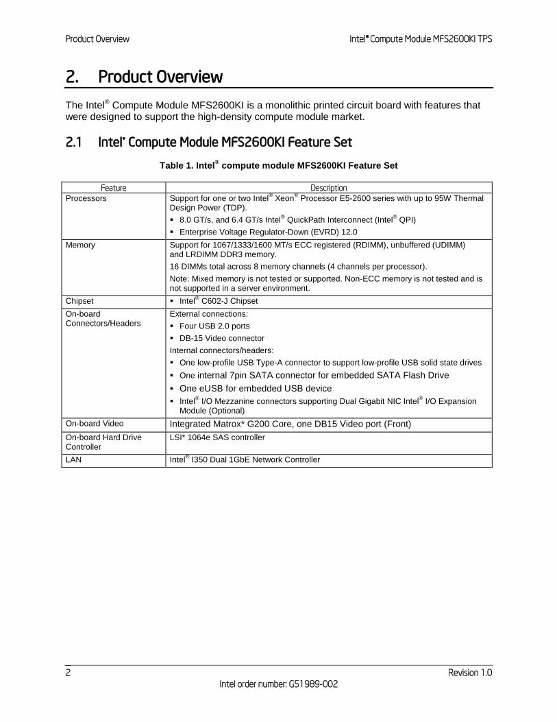
The following figure shows the board layout of the Intel® Compute Module MFS2600KI. Each connector and major component is identified by a number or letter. A description of each identified item is provided below the figure.
A CPU 1 DIMM Slots I CPU 1 Socket
B CPU 2 DIMM Slots J Power/Fault LEDs
C Mezzanine Card Connector 1 K Power Button
D Mezzanine Card Connector 2 L Battery
E Midplane Power Connector M Activity and ID LEDs
F Midplane Signal Connector N Video Connector
G Midplane Guide Pin Receptacle O USB Ports 2 and 3
H CPU 2 Socket P USB1 Ports 0 and 1
Figure 1. Component and Connector Location Diagram
Product Overview Intel® Compute Module MFS2600KI TPS
Revision 1.0
Intel order number: G51989-002
4
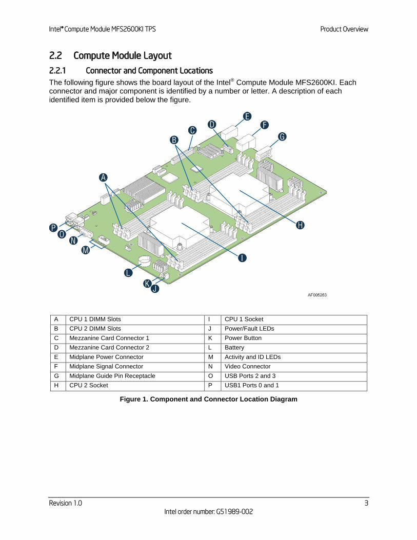
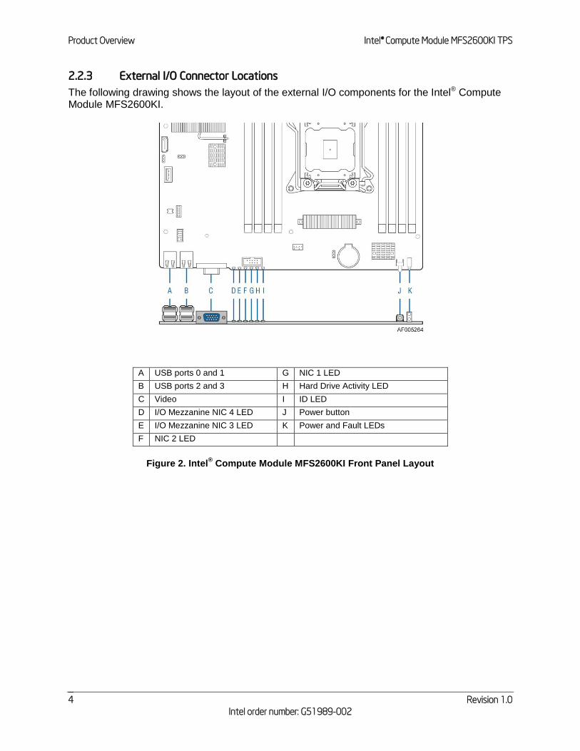
2.2.3 External I/O Connector Locations
The following drawing shows the layout of the external I/O components for the Intel® Compute Module MFS2600KI.
A USB ports 0 and 1 G NIC 1 LED
B USB ports 2 and 3 H Hard Drive Activity LED
C Video I ID LED
D I/O Mezzanine NIC 4 LED J Power button
E I/O Mezzanine NIC 3 LED K Power and Fault LEDs
F NIC 2 LED
Figure 2. Intel® Compute Module MFS2600KI Front Panel Layout
Intel® Compute Module MFS2600KI TPS Functional Architecture
Revision 1.0 5
Intel order number: G51989-002
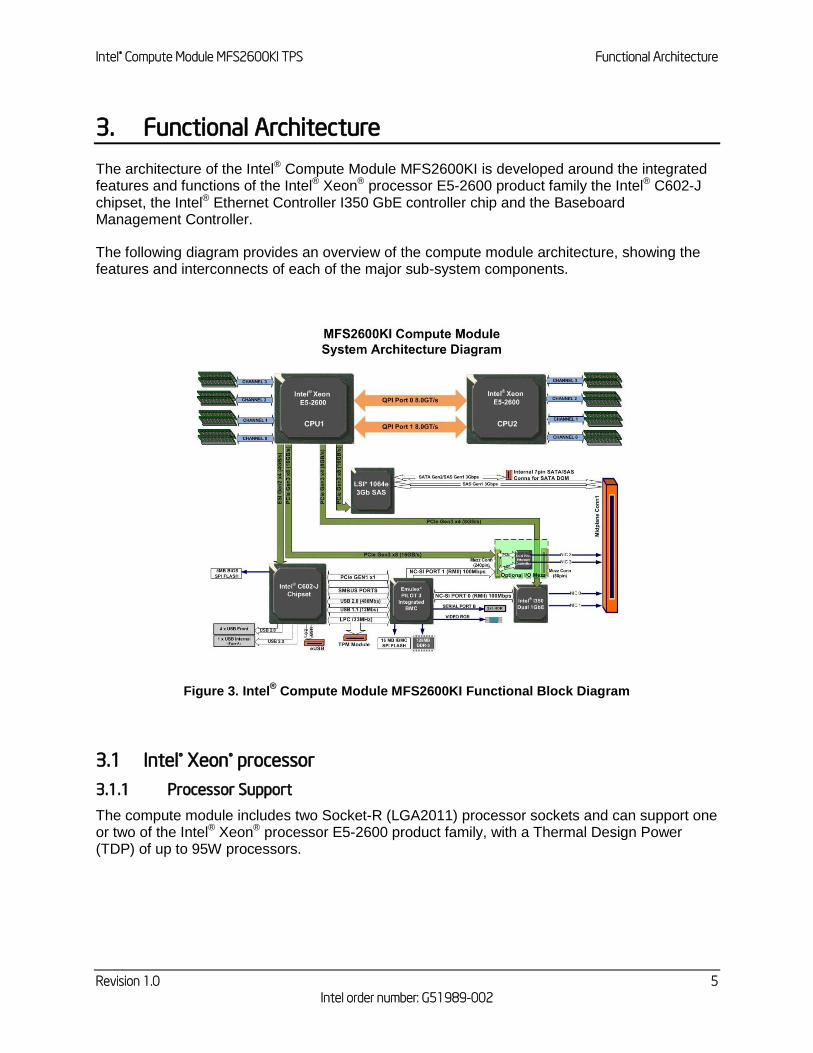
3. Functional Architecture
The architecture of the Intel® Compute Module MFS2600KI is developed around the integrated features and functions of the Intel® Xeon® processor E5-2600 product family the Intel® C602-J chipset, the Intel® Ethernet Controller I350 GbE controller chip and the Baseboard Management Controller.
The following diagram provides an overview of the compute module architecture, showing the features and interconnects of each of the major sub-system components.
Figure 3. Intel® Compute Module MFS2600KI Functional Block Diagram
3.1 Intel® Xeon® processor
3.1.1 Processor Support
The compute module includes two Socket-R (LGA2011) processor sockets and can support one or two of the Intel® Xeon® processor E5-2600 product family, with a Thermal Design Power (TDP) of up to 95W processors.
Functional Architecture Intel® Compute Module MFS2600KI TPS
Revision 1.0
Intel order number: G51989-002
6
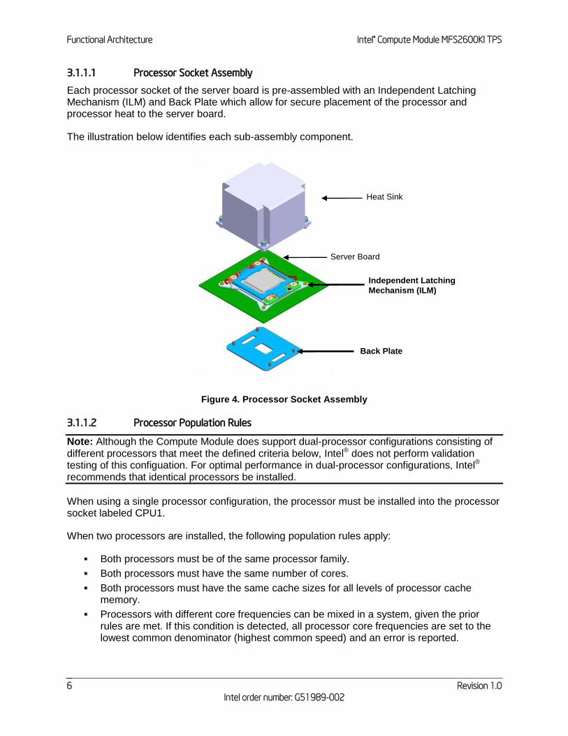
3.1.1.1 Processor Socket Assembly
Each processor socket of the server board is pre-assembled with an Independent Latching Mechanism (ILM) and Back Plate which allow for secure placement of the processor and processor heat to the server board.
The illustration below identifies each sub-assembly component.
Figure 4. Processor Socket Assembly
3.1.1.2 Processor Population Rules
Note: Although the Compute Module does support dual-processor configurations consisting of different processors that meet the defined criteria below, Intel® does not perform validation testing of this configuation. For optimal performance in dual-processor configurations, Intel® recommends that identical processors be installed.
When using a single processor configuration, the processor must be installed into the processor socket labeled CPU1.
When two processors are installed, the following population rules apply:
Both processors must be of the same processor family.
Both processors must have the same number of cores.
Both processors must have the same cache sizes for all levels of processor cache memory.
Processors with different core frequencies can be mixed in a system, given the prior rules are met. If this condition is detected, all processor core frequencies are set to the lowest common denominator (highest common speed) and an error is reported.
Heat Sink
Server Board
Independent Latching
Mechanism (ILM)
Back Plate

Intel® Compute Module MFS2600KI TPS Functional Architecture
Revision 1.0 7
Intel order number: G51989-002
Processors which have different Intel® Quickpath (QPI) Link Frequencies may operate together if they are otherwise compatible and if a common link frequency can be selected. The common link frequency would be the highest link frequency that all installed processors can achieve.
Processor stepping within a common processor family can be mixed as long as it is listed in the processor specification updates published by Intel Corporation.
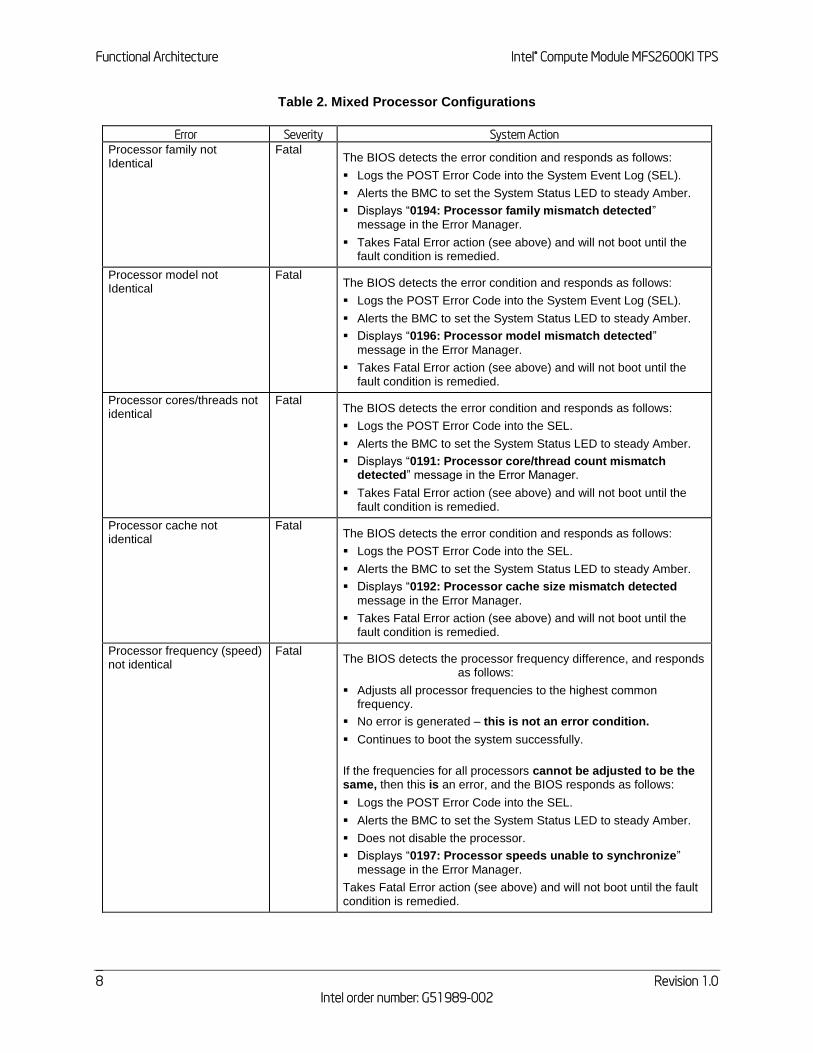
3.1.2 Processor Initialization Error Summary
The following table describes mixed processor conditions and recommended actions for the MFS2600KIdesigned around the Intel® Xeon® processor E5-2600 product family and Intel® C602-J chipset product family architecture. The errors fall into one of the following categories:
Fatal: If the system can boot, it pauses at a blank screen with the text “Unrecoverable fatal error found. System will not boot until the error is resolved” and “Press <F2> to enter setup”, regardless of whether the “Post Error Pause” setup option is enabled or disabled. When the operator presses the <F2> key on the keyboard, the error message is displayed on the Error Manager screen, and an error is logged to the System Event Log (SEL) with the POST Error Code. The system cannot boot unless the error is resolved. The user needs to replace the faulty part and restart the system. For Fatal Errors during processor initialization, the System Status LED will be set to a steady Amber color, indicating an unrecoverable system failure condition.
Major: If the “Post Error Pause” setup option is enabled, the system goes directly to the Error Manager to display the error, and logs the POST Error Code to SEL. Operator intervention is required to continue booting the system. Otherwise, if “POST Error Pause” is disabled, the system continues to boot and no prompt is given for the error, although the Post Error Code is logged to the Error Manager and in a SEL message.
Minor: The message is displayed on the screen or on the Error Manager screen, and the POST Error Code is logged to the SEL. The system continues booting in a degraded state. The user may want to replace the erroneous unit. The POST Error Pause option setting in the BIOS setup does not have any effect on this error.
Functional Architecture Intel® Compute Module MFS2600KI TPS
Revision 1.0
Intel order number: G51989-002
8
Table 2. Mixed Processor Configurations
Error Severity System Action
Processor family not Identical
Fatal The BIOS detects the error condition and responds as follows:
Logs the POST Error Code into the System Event Log (SEL).
Alerts the BMC to set the System Status LED to steady Amber.
Displays “0194: Processor family mismatch detected”
message in the Error Manager.
Takes Fatal Error action (see above) and will not boot until the fault condition is remedied.
Processor model not Identical
Fatal The BIOS detects the error condition and responds as follows:
Logs the POST Error Code into the System Event Log (SEL).
Alerts the BMC to set the System Status LED to steady Amber.
Displays “0196: Processor model mismatch detected”
message in the Error Manager.
Takes Fatal Error action (see above) and will not boot until the fault condition is remedied.
Processor cores/threads not identical
Fatal The BIOS detects the error condition and responds as follows:
Logs the POST Error Code into the SEL.
Alerts the BMC to set the System Status LED to steady Amber.
Displays “0191: Processor core/thread count mismatch detected” message in the Error Manager.
Takes Fatal Error action (see above) and will not boot until the fault condition is remedied.
Processor cache not identical
Fatal The BIOS detects the error condition and responds as follows:
Logs the POST Error Code into the SEL.
Alerts the BMC to set the System Status LED to steady Amber.
Displays “0192: Processor cache size mismatch detected
message in the Error Manager.
Takes Fatal Error action (see above) and will not boot until the fault condition is remedied.
Processor frequency (speed) not identical
Fatal The BIOS detects the processor frequency difference, and responds
as follows:
Adjusts all processor frequencies to the highest common frequency.
No error is generated – this is not an error condition.
Continues to boot the system successfully.
If the frequencies for all processors cannot be adjusted to be the same, then this is an error, and the BIOS responds as follows:
Logs the POST Error Code into the SEL.
Alerts the BMC to set the System Status LED to steady Amber.
Does not disable the processor.
Displays “0197: Processor speeds unable to synchronize”
message in the Error Manager.
Takes Fatal Error action (see above) and will not boot until the fault condition is remedied.
Intel® Compute Module MFS2600KI TPS Functional Architecture
Revision 1.0 9
Intel order number: G51989-002
Error Severity System Action
Processor Intel® QuickPath
Interconnect link frequencies not identical
Fatal The BIOS detects the QPI link frequencies and responds as follows:
Adjusts all QPI interconnect link frequencies to highest common frequency.
No error is generated – this is not an error condition.
Continues to boot the system successfully.
If the link frequencies for all QPI links cannot be adjusted to be the same, then this is an error, and the BIOS responds as follows:
Logs the POST Error Code into the SEL.
Alerts the BMC to set the System Status LED to steady Amber.
Displays “0195: Processor Intel® QPI link frequencies unable
to synchronize” message in the Error Manager.
Does not disable the processor.
Takes Fatal Error action (see above) and will not boot until the fault condition is remedied.
3.2 Processor Functions Overview
With the release of the Intel® Xeon® processor E5-2600 product family, several key system components, including the CPU, Integrated Memory Controller (IMC), and Integrated IO Module (IIO), have been combined into a single processor package and feature per socket; two Intel® QuickPath Interconnect point-to-point links capable of up to 8.0 GT/s, up to 40 lanes of Gen 3 PCI Express* links capable of 8.0 GT/s, and 4 lanes of DMI2/PCI Express* Gen 2 interface with a peak transfer rate of 5.0 GT/s. The processor supports up to 46 bits of physical address space and 48-bit of virtual address space. The following sections will provide an overview of the key processor features and functions that help to define the architecture, performance and supported functionality of the server board. For more comprehensive processor specific information, refer to the Intel® Xeon® processor E5-2600 product family documents listed in the Reference Document list in Chapter 1. Processor Core Features:
Up to 8 execution cores
Each core supports two threads (Intel® Hyper-Threading Technology), up to 16 threads
per socket
46-bit physical addressing and 48-bit virtual addressing
1 GB large page support for server applications
A 32-KB instruction and 32-KB data first-level cache (L1) for each core
A 256-KB shared instruction/data mid-level (L2) cache for each core
Up to 20 MB last level cache (LLC): up to 2.5 MB per core instruction/data last level cache (LLC), shared among all cores
Supported Technologies:
Intel® Virtualization Technology (Intel® VT)
Intel® Virtualization Technology for Directed I/O (Intel® VT-d)
Functional Architecture Intel® Compute Module MFS2600KI TPS
Revision 1.0
Intel order number: G51989-002
10
Intel® Trusted Execution Technology (Intel® TXT)
Intel® 64 Architecture
Intel® Streaming SIMD Extensions 4.1 (Intel® SSE4.1)
Intel® Streaming SIMD Extensions 4.2 (Intel® SSE4.2)
Intel® Advanced Vector Extensions (Intel® AVX)
Intel® Hyper-Threading Technology
Execute Disable Bit
Intel® Turbo Boost Technology
Intel® Intelligent Power Technology
Enhanced Intel® SpeedStep Technology
3.2.1 Intel® QuickPath Interconnect
The Intel® QuickPath Interconnect (QPI) is a high speed, packetized, point-to-point interconnect used in the processor. The narrow high-speed links stitch together processors in distributed shared memory and integrated I/O platform architecture. It offers much higher bandwidth with low latency. The Intel® QuickPath Interconnect has an efficient architecture allowing more interconnect performance to be achieved in real systems. It has a snoop protocol optimized for low latency and high scalability, as well as packet and lane structures enabling quick completions of transactions. Reliability, availability, and serviceability features (RAS) are built into the architecture. The physical connectivity of each interconnect link is made up of twenty differential signal pairs plus a differential forwarded clock. Each port supports a link pair consisting of two uni-directional links to complete the connection between two components. This supports traffic in both directions simultaneously. To facilitate flexibility and longevity, the interconnect is defined as having five layers: Physical, Link, Routing, Transport, and Protocol. The Intel® QuickPath Interconnect includes a cache coherency protocol to keep the distributed memory and caching structures coherent during system operation. It supports both low-latency source snooping and a scalable home snoop behavior. The coherency protocol provides for direct cache-to-cache transfers for optimal latency.
3.2.2 Intel® Hyper-Threading Technology
Most Intel® Xeon® processors support Intel® Hyper-Threading Technology. The BIOS detects processors that support this feature and enables the feature during POST.
If the processor supports this feature, the BIOS Setup provides an option to enable or disable this feature. The default is enabled.
3.3 Processor Integrated I/O Module (IIO)
The processor’s integrated I/O module provides features traditionally supported through chipset components. The integrated I/O module provides the following features:
3.3.1 PCI Express Interfaces
The integrated I/O module incorporates the PCI Express interface and supports up to 40 lanes of PCI Express. The following tables list the CPU PCIe port connectivity of the Intel® Compute Module MFS2600KI.
Intel® Compute Module MFS2600KI TPS Functional Architecture
Revision 1.0 11
Intel order number: G51989-002
Table 3. Intel® Compute Module MFS2600KI PCIe Bus Segment Characteristics
CPU# Device Physical Connector Electrical
Width
CPU1 Intel® C602-J N/A x4 Gen2
CPU1 IO Mezzanine Card
120 pin
Mezzanine Card
Connector
x8 Gen2
CPU1 Intel® I350 NIC N/A x4 Gen2
CPU1 LSI* 1064e SAS N/A x8 Gen1
3.3.2 DMI2 Interface to the PCH
The platform requires an interface to the legacy Southbridge (PCH) which provides basic, legacy functions required for the server platform and operating systems. Since only one PCH is required and allowed for the system, CPU2 which does not connect to PCH would use this port as a standard x4 PCI Express 2.0 interface.
3.3.3 Integrated IOAPIC
Provides support for PCI Express devices implementing legacy interrupt messages without interrupt sharing.
3.3.4 Intel® QuickData Technology
Used for efficient, high bandwidth data movement between two locations in memory or from memory to I/O.
3.4 Memory Subsystem
3.4.1 Integrated Memory Controller (IMC) and Memory Subsystem
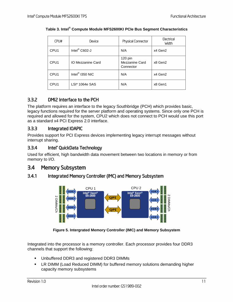
Figure 5. Intergrated Memory Controller (IMC) and Memory Subsystem
Integrated into the processor is a memory controller. Each processor provides four DDR3 channels that support the following:
Unbuffered DDR3 and registered DDR3 DIMMs
LR DIMM (Load Reduced DIMM) for buffered memory solutions demanding higher capacity memory subsystems
CPU 2 CPU 1
2 D
IMM
s/C
h
2 D
IMM
s/C
h
Functional Architecture Intel® Compute Module MFS2600KI TPS
Revision 1.0
Intel order number: G51989-002
12
Independent channel mode or lockstep mode
Data burst length of eight cycles for all memory organization modes
Memory DDR3 data transfer rates of 800, 1066, 1333, and 1600 MT/s
64-bit wide channels plus 8-bits of ECC support for each channel
DDR3 standard I/O Voltage of 1.5 V and DDR3 Low Voltage of 1.35 V
1-Gb, 2-Gb, and 4-Gb DDR3 DRAM technologies supported for these devices:
o UDIMM DDR3 – SR x8 and x16 data widths, DR – x8 data width
o RDIMM DDR3 – SR,DR, and QR – x4 and x8 data widths
o LRDIMM DDR3 – QR – x4 and x8 data widths with direct map or with rank multiplication
Up to eight ranks supported per memory channel, 1, 2 or 4 ranks per DIMM
Open with adaptive idle page close timer or closed page policy
Per channel memory test and initialization engine can initialize DRAM to all logical zeros with valid ECC (with or without data scrambler) or a predefined test pattern
Isochronous access support for Quality of Service (QoS)
Minimum memory configuration: independent channel support with 1 DIMM populated
Integrated dual SMBus* master controllers
Command launch modes of 1n/2n
RAS Support:
o Rank Level Sparing and Device Tagging
o Demand and Patrol Scrubbing
o DRAM Single Device Data Correction (SDDC) for any single x4 or x8 DRAM device. Independent channel mode supports x4 SDDC. x8 SDDC requires lockstep mode
o Lockstep mode where channels 0 and 1 and channels 2 and 3 are operated in lockstep mode
o Data scrambling with address to ease detection of write errors to an incorrect address.
o Error reporting through Machine Check Architecture
o Read Retry during CRC error handling checks by iMC
o Channel mirroring within a socket
CPU1 Channel Mirror Pairs (A,B) and (C,D)
CPU2 Channel Mirror Pairs (E,F) and (G,H)
o Error Containment Recovery
Improved Thermal Throttling with dynamic Closed Loop Thermal Throttling (CLTT)
Memory thermal monitoring support for DIMM temperature
3.4.1.1 Intel® Compute Module MFS2600KI Supported Memory
Each processor provides four banks of memory, each capable of supporting up to two DIMMs.
DIMMs are organized into physical slots on DDR3 memory channels that belong to processor sockets.
The memory channels from processor socket 1 are identified as Channel A, B, C, and D. The memory channels from processor socket 2 are identified as Channel E, F, G, and H.
Intel® Compute Module MFS2600KI TPS Functional Architecture
Revision 1.0 13
Intel order number: G51989-002
The silk screened DIMM slot identifiers on the board provide information about the channel, and therefore the processor to which they belong. For example, DIMM_A1 is the first slot on Channel A on processor 1; DIMM_E1 is the first DIMM socket on Channel E on processor 2.
The memory slots associated with a given processor are unavailable if the corresponding processor socket is not populated.
A processor may be installed without populating the associated memory slots provided and a second processor is installed with associated memory. In this case, the memory is shared by the processors. However, the platform suffers performance degradation and latency due to the remote memory.
Processor sockets are self-contained and autonomous. However, all memory subsystem support (such as Memory RAS, Error Management,) in the BIOS setup are applied commonly across processor sockets.
For a complete list of supported memory for the Intel® Compute Module MFS2600KI, refer to the Tested Memory List published in the Intel® Server Configurator Tool.
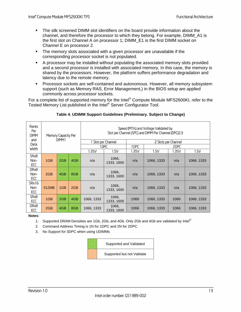
Table 4. UDIMM Support Guidelines (Preliminary. Subject to Change)
Ranks
Per
DIMM
and
Data
Width
Memory Capacity Per
DIMM1
Speed (MT/s) and Voltage Validated by
Slot per Channel (SPC) and DIMM Per Channel (DPC)2,3
1 Slot per Channel 2 Slots per Channel
1DPC 1DPC 2DPC
1.35V 1.5V 1.35V 1.5V 1.35V 1.5V
SRx8
Non-
ECC
1GB 2GB 4GB n/a 1066,
1333, 1600 n/a 1066, 1333 n/a 1066, 1333
DRx8
Non-
ECC
2GB 4GB 8GB n/a 1066,
1333, 1600 n/a 1066, 1333 n/a 1066, 1333
SRx16
Non-
ECC
512MB 1GB 2GB n/a 1066,
1333, 1600 n/a 1066, 1333 n/a 1066, 1333
SRx8
ECC 1GB 2GB 4GB 1066, 1333
1066, 1333, 1600
1066 1066, 1333 1066 1066, 1333
DRx8
ECC 2GB 4GB 8GB 1066, 1333
1066, 1333, 1600
1066 1066, 1333 1066 1066, 1333
Notes:
1. Supported DRAM Densities are 1Gb, 2Gb, and 4Gb. Only 2Gb and 4Gb are validated by Intel®
2. Command Address Timing is 1N for 1DPC and 2N for 2DPC
3. No Support for 3DPC when using UDIMMs
Supported and Validated
Supported but not Validate
Functional Architecture Intel® Compute Module MFS2600KI TPS
Revision 1.0
Intel order number: G51989-002
14
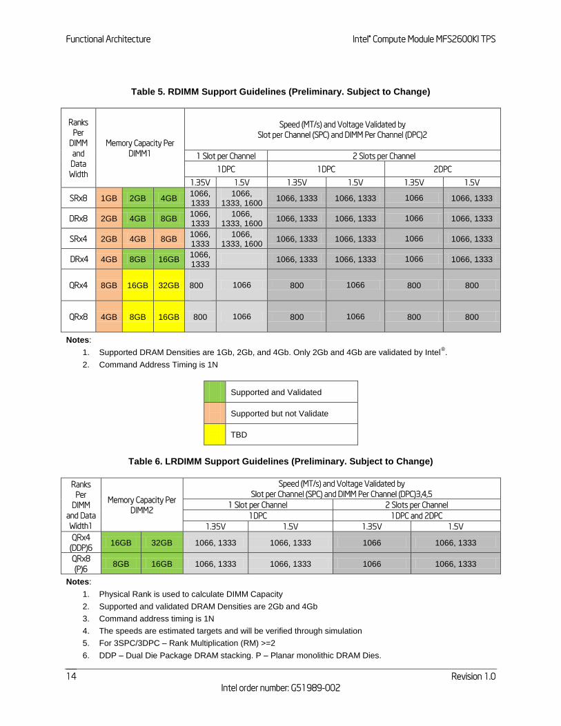
Table 5. RDIMM Support Guidelines (Preliminary. Subject to Change)
Ranks
Per
DIMM
and
Data
Width
Memory Capacity Per
DIMM1
Speed (MT/s) and Voltage Validated by
Slot per Channel (SPC) and DIMM Per Channel (DPC)2
1 Slot per Channel 2 Slots per Channel
1DPC 1DPC 2DPC
1.35V 1.5V 1.35V 1.5V 1.35V 1.5V
SRx8 1GB 2GB 4GB 1066, 1333
1066, 1333, 1600
1066, 1333 1066, 1333 1066 1066, 1333
DRx8 2GB 4GB 8GB 1066, 1333
1066, 1333, 1600
1066, 1333 1066, 1333 1066 1066, 1333
SRx4 2GB 4GB 8GB 1066, 1333
1066, 1333, 1600
1066, 1333 1066, 1333 1066 1066, 1333
DRx4 4GB 8GB 16GB 1066, 1333
1066, 1333 1066, 1333 1066 1066, 1333
QRx4 8GB 16GB 32GB
800
1066 800 1066 800 800
QRx8
4GB 8GB 16GB 800 1066 800 1066 800 800
Notes:
1. Supported DRAM Densities are 1Gb, 2Gb, and 4Gb. Only 2Gb and 4Gb are validated by Intel®.
2. Command Address Timing is 1N
Supported and Validated
Supported but not Validate
TBD
Table 6. LRDIMM Support Guidelines (Preliminary. Subject to Change)
Ranks
Per
DIMM
and Data
Width1
Memory Capacity Per
DIMM2
Speed (MT/s) and Voltage Validated by
Slot per Channel (SPC) and DIMM Per Channel (DPC)3,4,5
1 Slot per Channel 2 Slots per Channel
1DPC 1DPC and 2DPC
1.35V 1.5V 1.35V 1.5V
QRx4
(DDP)6 16GB 32GB 1066, 1333 1066, 1333 1066 1066, 1333
QRx8
(P)6 8GB 16GB 1066, 1333 1066, 1333 1066 1066, 1333
Notes:
1. Physical Rank is used to calculate DIMM Capacity
2. Supported and validated DRAM Densities are 2Gb and 4Gb
3. Command address timing is 1N
4. The speeds are estimated targets and will be verified through simulation
5. For 3SPC/3DPC – Rank Multiplication (RM) >=2
6. DDP – Dual Die Package DRAM stacking. P – Planar monolithic DRAM Dies.
Intel® Compute Module MFS2600KI TPS Functional Architecture
Revision 1.0 15
Intel order number: G51989-002
Supported and Validated
3.4.2 Publishing Compute Module Memory
The BIOS displays the “Total Memory” of the compute module during POST if Display Logo is disabled in the BIOS setup. This is the total size of memory discovered by the BIOS during POST, and is the sum of the individual sizes of installed DDR3 DIMMs in the system.
The BIOS displays the “Effective Memory” of the compute module in the BIOS setup. The term Effective Memory refers to the total size of all DDR3 DIMMs that are active (not disabled) and not used as redundant units.
The BIOS provides the total memory of the compute module in the main page of the BIOS setup. This total is the same as the amount described by the first bullet above.
If Display Logo is disabled, the BIOS displays the total system memory on the diagnostic screen at the end of POST. This total is the same as the amount described by the first bullet above.
3.4.3 Memory Map and Population Rules
The following are generic DIMM population requirements that generally apply to the Intel® Compute Module MFS2600KI.
DIMM slots on any memory channel must be filled following the “farthest fill first” rule.
A maximum of eight ranks can be installed on any one channel, counting all ranks in each DIMM on the channel.
DIMM types (UDIMM, RDIMM, LRDIMM) must not be mixed within or across processor sockets.
Mixing ECC with non-ECC DIMMs (UDIMMs) is not supported within or across processor sockets.
Mixing Low Voltage (1.35V) DIMMs with Standard Voltage (1.5V) DIMMs is not supported within or across processor sockets.
Mixing DIMMs of different frequencies and latencies is not supported within or across processor sockets.
LRDIMM Rank Multiplication Mode and Direct Map Mode must not be mixed within or across processor sockets.
Only ECC UDIMMs support Low Voltage 1.35V operation.
QR RDIMMs may only be installed in DIMM Slot 1 or 2 on a channel.
Two DPC QR Low Voltage RDIMMs are not supported.
In order to install 3 QR LRDIMMs on the same channel, they must be operated with Rank Multiplication as RM = 2.
RAS Modes Lockstep, Rank Sparing, and Mirroring are mutually exclusive in this BIOS. Only one operating mode may be selected, and it will be applied to the entire system.
If a RAS Mode has been configured, and the memory population will not support it during boot, the system will fall back to Independent Channel Mode and log and display errors
Functional Architecture Intel® Compute Module MFS2600KI TPS
Revision 1.0
Intel order number: G51989-002
16
Rank Sparing Mode is only possible when all channels that are populated with memory meet the requirement of having at least two SR or DR DIMM installed, or at least one QR DIMM installed, on each populated channel.
Lockstep or Mirroring Modes require that for any channel pair that is populated with memory, the memory population on both channels of the pair must be identically sized.
DIMM population rules require that DIMMs within a channel be populated starting with the BLUE DIMM slot or DIMM farthest from the processor in a “fill-farthest” approach. In addition, when populating a Quad-rank DIMM with a Single- or Dual-rank DIMM in the same channel, the Quad-rank DIMM must be populated farthest from the processor.
Table 7. DDR3 RDIMM Population within a Channel
Configuration
Number
Speed
1N or 2N
DIMM 2
DIMM 1
(Blue Slot)
1 DDR3-1333, and 1066 1N Empty Single-rank
2 DDR3-1333, and 1066 1N Empty Dual-rank
3 DDR3-1066 1N Empty Quad-rank
4 DDR3-1333, and 1066 1N Single-rank Single-rank
5 DDR3-1333, and 1066 1N Single-rank Dual-rank
6 DDR3-1333, and 1066 1N Dual-rank Dual-rank
7 DDR3-800 1N Single-rank Quad-rank
8 DDR3-800 1N Dual-rank Quad-rank
9 DDR3-800 1N Quad-rank Quad-rank
10 DDR3-800 1N Single-rank Single-rank
11 DDR3-800 1N Single-rank Dual-rank
12 DDR3-800 1N Dual-rank Dual-rank
13 DDR3-800 1N Dual-rank Dual-rank
14 DDR3-800 1N Single-rank Quad-rank
15 DDR3-800 1N Dual-rank Quad-rank
16 DDR3-800 1N Dual-rank Quad-rank
Table 8. DDR3L Low Voltage RDIMM Population within a Channel
Configuration
Number
Speed
1N or 2N
DIMM 2
DIMM 1
(Blue Slot)
1 DDR3L-1333, 1066 1N Empty Single-rank
2 DDR3L-1333, 1066 1N Empty Dual-rank
3 DDR3L-800 1N Empty Quad-rank
4 DDR3L-1066 1N Single-rank Single-rank
5 DDR3L-1066 1N Single-rank Dual-rank
6 DDR3L-1066 1N Dual-rank Dual-rank
7 DDR3L- 800 1N Single-rank Quad-rank

Intel® Compute Module MFS2600KI TPS Functional Architecture
Revision 1.0 17
Intel order number: G51989-002
Table 9. DDR3 UDIMM Population within a Channel
Configuration
Number
Speed
1N or 2N
DIMM 2 DIMM 1
(Blue Slot)
1 DDR3-1333, and 1066 1N Empty Single-rank
2 DDR3-1333, and 1066 1N Empty Dual-rank
3 DDR3-1333, and 1066 2N Single-rank Single-rank
4 DDR3-1333, and 1066 2N Single-rank Dual-rank
5 DDR3-1333, and 1066 2N Dual-rank Dual-rank
Table 10. DDR3L Low Voltage UDIMM Poplulation within a Channel
Configuration
Number
Speed
1N or 2N
DIMM 2 DIMM 1
(Blue Slot)
1 DDR3-1333,1066 1N Empty Single-rank
2 DDR3-1333, 1066 1N Empty Dual-rank
3 DDR3-1066 2N Single-rank Single-rank
4 DDR3-1066 2N Single-rank Dual-rank
5 DDR3-1066 2N Dual-rank Dual-rank
Functional Architecture Intel® Compute Module MFS2600KI TPS
Revision 1.0
Intel order number: G51989-002
18
Figure 6. DIMM Slot Order
3.4.3.1 Memory Subsystem Nomenclature
The nomenclature for DIMM sockets implemented on the Intel® Compute Module MFS2600KI is detailed in the following table.
Table 11. Intel® Compute Module MFS2600KI DIMM Nomenclature
Processor Socket 1 Processor Socket 2
(0)
Channel A
(1)
Channel B
(2)
Channel C
(3)
Channel D
(0)
Channel E
(1)
Channel F
(2)
Channel G
(3)
Channel H
A1 A2 B1 B2 C1 C2 D1 D2 E1 E2 F1 F2 G1 G2 H1 H2
Intel® Compute Module MFS2600KI TPS Functional Architecture
Revision 1.0 19
Intel order number: G51989-002
3.4.3.2 Publishing System Memory
The BIOS displays the “Total Memory” of the system during POST if Quite Boot is disabled in the BIOS setup. This is the total size of memory discovered by the BIOS during POST, and is the sum of the individual sizes of installed DDR3 DIMMs in the system.
The BIOS displays the “Effective Memory” of the system in the BIOS setup. The term Effective Memory refers to the total size of all DDR3 DIMMs that are active (not disabled) and not used as redundant units.
The BIOS provides the total memory of the system in the main page of the BIOS setup. This total is the same as the amount described by the first bullet above.
If Quite Boot is disabled, the BIOS displays the total system memory on the diagnostic screen at the end of POST. This total is the same as the amount described by the first bullet above.
3.4.4 Memory RAS
3.4.4.1 RAS Features
The Compute Module supports the following memory RAS features:
Independent Channel Mode
Rank Sparing Mode
Mirrored Channel Mode
Lockstep Channel Mode
Regardless of RAS mode, the requirements for populating within a channel given in the section 3.3.3 must be met at all times. Note that support of RAS modes that require matching DIMM population between channels (Mirrored and Lockstep) require that ECC DIMMs be populated. Independent Channel Mode is the only mode that supports non-ECC DIMMs in addition to ECC DIMMs.
For RAS modes that require matching populations, the same slot positions across channels must hold the same DIMM type with regards to size and organization. DIMM timings do not have to match but timings will be set to support all DIMMs populated (that is, DIMMs with slower timings will force faster DIMMs to the slower common timing modes).
3.4.4.2 Independent Channel Mode
Channels can be populated in any order in Independent Channel Mode. All four channels may be populated in any order and have no matching requirements. All channels must run at the same interface frequency but individual channels may run at different DIMM timings (RAS latency, CAS Latency, and so forth).
3.4.4.3 Rank Sparing Mode
In Rank Sparing Mode, one rank is a spare of the other ranks on the same channel. The spare rank is held in reserve and is not available as system memory. The spare rank must have identical or larger memory capacity than all the other ranks (sparing source ranks) on the same channel. After sparing, the sparing source rank will be lost.
Functional Architecture Intel® Compute Module MFS2600KI TPS
Revision 1.0
Intel order number: G51989-002
20
3.4.4.4 Mirrored Channel Mode
In Mirrored Channel Mode, the memory contents are mirrored between Channel 0 and Channel 2 and also between Channel 1 and Channel 3. As a result of the mirroring, the total physical memory available to the system is half of what is populated. Mirrored Channel Mode requires that Channel 0 and Channel 2, and Channel 1 and Channel 3 must be populated identically with regards to size and organization. DIMM slot populations within a channel do not have to be identical but the same DIMM slot location across Channel 0 and Channel 2 and across Channel 1 and Channel 3 must be populated the same.
3.4.4.5 Lockstep Channel Mode
In Lockstep Channel Mode, each memory access is a 128-bit data access that spans Channel 0 and Channel 1, and Channel 2 and Channel 3. Lockstep Channel mode is the only RAS mode that allows SDDC for x8 devices. Lockstep Channel Mode requires that Channel 0 and Channel 1, and Channel 2 and Channel 3 must be populated identically with regards to size and organization. DIMM slot populations within a channel do not have to be identical but the same DIMM slot location across Channel 0 and Channel 1 and across Channel 2 and Channel 3 must be populated the same.
3.5 Intel® C602-J Chipset Overvew
The Intel® C602-J chipset in the Intel® Compute Module MFS2600KI provide a connection point between various I/O components and Intel® Xeon E5-2600 processors, which includes the following core platform functions:
Digital Media Interface (DMI)
PCI Express* Interface
Serial ATA (SATA) Controller
Serial Attached SCSI (SAS)/SATA Controller
AHCI
Rapid Storage Technology
PCI Interface
Low Pin Count (LPC) Interface
Serial Peripheral Interface (SPI)
Compatibility Modules (DMA Controller, Timer/Counters, Interrupt Controller)
Advanced Programmable Interrupt Controller (APIC)
Universal Serial Bus (USB) Controllers
Gigabit Ethernet Controller
RTC
GPIO
Enhanced Power Management
Intel® Active Management Technology (Intel® AMT)
Manageability
System Management Bus (SMBus* 2.0)
Integrated NVSRAM controller
Virtualization Technology for Directed I/O (Intel® VT-d)

Intel® Compute Module MFS2600KI TPS Functional Architecture
Revision 1.0 21
Intel order number: G51989-002
JTAG Boundary-Scan
KVM/Serial Over LAN (SOL) Function
3.5.1 Digital Media Interface (DMI)
Digital Media Interface (DMI) is the chip-to-chip connection between the processor and Intel® C602-J chipset. This high-speed interface integrates advanced priority-based servicing allowing for concurrent traffic and true isochronous transfer capabilities. Base functionality is completely software-transparent, permitting current and legacy software to operate normally.
3.5.2 PCI Express* Interface
The Intel® C602-J chipset provides up to eight PCI Express Root Ports, supporting the PCI Express Base Specification, Revision 2.0. Each Root Port x1 lane supports up to 5 Gb/s bandwidth in each direction (10 Gb/s concurrent). PCI Express Root Ports 1-4 or Ports 5-8 can independently be configured to support four x1s, two x2s, one x2 and two x1s, or one x4 port widths.
3.5.3 Serial ATA (SATA) Controller
The Intel® C602-J chipset has two integrated SATA host controllers that support independent DMA operation on up to six ports and supports data transfer rates of up to 6.0 Gb/s (600 MB/s) on up to two ports (Port 0 and 1 Only) while all ports support rates up to 3.0 Gb/s (300 MB/s) and up to 1.5 Gb/s (150 MB/s). The SATA controller contains two modes of operation – a legacy mode using I/O space, and an AHCI mode using memory space. Software that uses legacy mode will not have AHCI capabilities.
The Intel® C602-J chipset supports the Serial ATA Specification, Revision 3.0. The Intel® C602-J also supports several optional sections of the Serial ATA II: Extensions to Serial ATA 1.0 Specification, Revision 1.0 (AHCI support is required for some elements).
3.5.4 Low Pin Count (LPC) Interface
The Intel® C602-J chipset implements an LPC Interface as described in the LPC 1.1 Specification. The Low Pin Count (LPC) bridge function of the Intel® C602-J resides in PCI Device 31: Function 0. In addition to the LPC bridge interface function, D31:F0 contains other functional units including DMA, interrupt controllers, timers, power management, system management, GPIO, and RTC.
3.5.5 Serial Peripheral Interface (SPI)
The Intel® C602-J chipset implements an SPI Interface as an alternative interface for the BIOS flash device. The SPI flash is required to support Gigabit Ethernet and Intel® Active Management Technology. The Intel® C602-J chipset supports up to two SPI flash devices with speeds up to 50 MHz.
3.5.6 Advanced Programmable Interrupt Controller (APIC)
In addition to the standard ISA compatible Programmable Interrupt controller (PIC) described in the previous section, the Intel® C602-J incorporates the Advanced Programmable Interrupt Controller (APIC).
Functional Architecture Intel® Compute Module MFS2600KI TPS
Revision 1.0
Intel order number: G51989-002
22
3.5.7 Universal Serial Bus (USB) Controllers
The Intel® C602-J chipset has up to two Enhanced Host Controller Interface (EHCI) host controllers that support USB high-speed signaling. High-speed USB 2.0 allows data transfers up to 480 Mb/s which is 40 times faster than full-speed USB. The Intel® C602-J chipset supports up to fourteen USB 2.0 ports. All fourteen ports are high-speed, full-speed, and low-speed capable.
Four external connectors are located on the front of the compute module.
One internal 2x5 header is provided, capable of supporting a low-profile USB solid state drive.
Two ports are routed to the Integrated BMC to support rKVM.
3.6 Integrated Baseboard Management Controller Overview
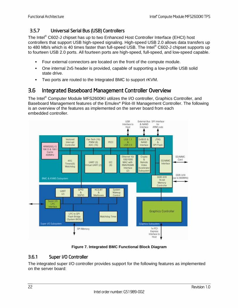
The Intel® Computer Module MFS2600KI utilizes the I/O controller, Graphics Controller, and Baseboard Management features of the Emulex* Pilot-III Management Controller. The following is an overview of the features as implemented on the server board from each embedded controller.
Figure 7. Integrated BMC Functional Block Diagram
3.6.1 Super I/O Controller
The integrated super I/O controller provides support for the following features as implemented on the server board:
Intel® Compute Module MFS2600KI TPS Functional Architecture
Revision 1.0 23
Intel order number: G51989-002
Two Fully Functional Serial Ports, compatible with the 16C550
Serial IRQ Support
Up to 16 Shared direct GPIO’s
Serial GPIO support for 80 general purpose inputs and 80 general purpose outputs available for host processor
Programmable Wake-up Event Support
Plug and Play Register Set
Power Supply Control
Host SPI bridge for system BIOS support
3.6.1.1 Keyboard and Mouse Support
The Intel® Computer Module MFS2600KI does not support PS/2 interface keyboards and mice. However, the system BIOS recognizes USB specification-compliant keyboard and mice.
3.6.1.2 Wake-up Control
The super I/O contains functionality that allows various events to power on and power off the system.
3.6.2 Graphics Controller and Video Support
The integrated graphics controller provides support for the following features as implemented on the server board:
Integrated Graphics Core with 2D Hardware accelerator
DDR-3 memory interface with 16 MB of memory allocated and reported for graphics memory
High speed Integrated 24-bit RAMDAC
Single lane PCI-Express host interface running at Gen 1 speed
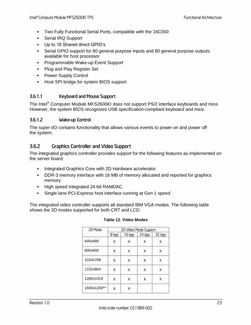
The integrated video controller supports all standard IBM VGA modes. The following table shows the 2D modes supported for both CRT and LCD:
Table 12. Video Modes
2D Mode 2D Video Mode Support
8 bpp 16 bpp 24 bpp 32 bpp
640x480 X X X X
800x600 X X X X
1024x768 X X X X
1152x864 X X X X
1280x1024 X X X X
1600x1200** X X
Functional Architecture Intel® Compute Module MFS2600KI TPS
Revision 1.0
Intel order number: G51989-002
24
** Video resolutions at 1600x1200 and higher are only supported through the external video connector located on the rear I/O section of the server board. Utilizing the optional front panel video connector may result in lower video resolutions.
The server board provides two video interfaces. The primary video interface is accessed using a standard 15-pin VGA connector found on the back edge of the server board. In addition, video signals are routed to a 14-pin header labeled “FP_Video” on the leading edge of the server board, allowing for the option of cabling to a front panel video connector. Attaching a monitor to the front panel video connector will disable the primary external video connector on the back edge of the board.
The BIOS supports dual-video mode when an add-in video card is installed.
In the single mode (dual monitor video = disabled), the on-board video controller is disabled when an add-in video card is detected.
In the dual mode (on-board video = enabled, dual monitor video = enabled), the on-board video controller is enabled and is the primary video device. The add-in video card is allocated resources and is considered the secondary video device. The BIOS Setup utility provides options to configure the feature as follows:
Table 13. Video mode
On-board Video Enabled
Disabled
Dual Monitor Video Enabled
Disabled
Shaded if on-board video is set to "Disabled"
3.6.3 Baseboard Management Controller
The server board utilizes the following features of the embedded baseboard management controller.
IPMI 2.0 Compliant
400MHz 32-bit ARM9 processor with memory management unit (MMU)
Two independent10/100/1000 Ethernet Controllers with RMII/RGMII support
DDR2/3 16-bit interface with up to 800 MHz operation
12 10-bit ADCs
Fourteen fan tachometers
Eight Pulse Width Modulators (PWM)
Chassis intrusion logic
JTAG Master
Eight I2C interfaces with master-slave and SMBus* timeout support. All interfaces are SMBus* 2.0 compliant.
Parallel general-purpose I/O Ports (16 direct, 32 shared)
Serial general-purpose I/O Ports (80 in and 80 out)
Three UARTs
Platform Environmental Control Interface (PECI)
Six general-purpose timers
Intel® Compute Module MFS2600KI TPS Functional Architecture
Revision 1.0 25
Intel order number: G51989-002
Interrupt controller
Multiple SPI flash interfaces
NAND/Memory interface
Sixteen mailbox registers for communication between the BMC and host
LPC ROM interface
BMC watchdog timer capability
SD/MMC card controller with DMA support
LED support with programmable blink rate controls on GPIOs
Port 80h snooping capability
Secondary Service Processor (SSP), which provides the HW capability of off-loading time critical processing tasks from the main ARM core.
3.6.3.1 Remote Keyboard, Video, Mouse, and Storage (KVMS) Support
USB 2.0 interface for Keyboard, Mouse and Remote storage such as CD/DVD ROM and floppy
USB 1.1/USB 2.0 interface for PS2 to USB bridging, remote Keyboard and Mouse
Hardware Based Video Compression and Redirection Logic
Supports both text and Graphics redirection
Hardware assisted Video redirection using the Frame Processing Engine
Direct interface to the Integrated Graphics Controller registers and Frame buffer
Hardware-based encryption engine
3.6.3.2 Integrated BMC Embedded LAN Channel
The Integrated BMC hardware includes two dedicated 10/100 network interfaces. These interfaces are not shared with the host system. At any time, only one dedicated interface may be enabled for management traffic. The default active interface is the NIC 1 port.
3.7 Network Interface Controller (NIC)
Network interface support is provided from the on-board Intel® I350 NIC, which is a single, compact component with two fully integrated GbE Media Access Control (MAC) and Physical Layer (PHY) ports. The on-board Intel® I350 NIC provides the Compute Module with support for dual LAN ports designed for 1000 Mbps operation.
The Intel® I350 device provides two standard IEEE 802.3 Ethernet interface through its SERDES interfaces. Each network interface controller (NIC) drives two LEDs (1 per port) located on the front panel. The LED indicates transmit/receive activity when blinking.
Table 14. NIC LED BEHAVIOR
LED Color LED State NIC State
Green On Link
Blinking Transmit / Receive activity
Functional Architecture Intel® Compute Module MFS2600KI TPS
Revision 1.0
Intel order number: G51989-002
26
Intel® I350 NIC will be used in conjunction with the Emulex* Pilot-III Management Controller for out of band Management traffic. The BMC will communicate with Intel® I350 NIC over a NC-SI interface (RMII physical). Intel® I350 NIC will be on standby power so that the BMC can send management traffic over the NC-SI interface to the network during sleep state S5.
3.8 Intel® Virtualization Technology for Directed I/O (Intel® VT-d)
The Intel® C602-J chipset provides hardware support for implementation of Intel® Virtualization Technology with Directed I/O (Intel® VT-d). Intel® VT-d consists of technology components that support the virtualization of platforms based on Intel® Architecture Processors. Intel® VT-d Technology enables multiple operating systems and applications to run in independent partitions. A partition behaves like a virtual machine (VM) and provides isolation and protection across partitions. Each partition is allocated its own subset of host physical memory.

Intel® Compute Module MFS2600KI TPS System Security
Revision 1.0 27
Intel order number: G51989-002
4. System Security
4.1 BIOS Password Protection
The BIOS uses passwords to prevent unauthorized tampering with the server setup. Passwords can restrict entry to the BIOS Setup, restrict use of the Boot Popup menu, and suppress automatic USB device reordering. There is also an option to require a Power On password entry in order to boot the system. If the Power On Password function is enabled in Setup, the BIOS will halt early in POST to request a password before continuing POST. Both Administrator and User passwords are supported by the BIOS. An Administrator password must be installed in order to set the User password. The maximum length of a password is 14 characters. A password can have alphanumeric (a-z, A-Z, 0-9) characters and it is case sensitive. Certain special characters are also allowed, from the following set:
! @ # $ % ^ & * ( ) - _ + = ? The Administrator and User passwords must be different from each other. An error message will be displayed if there is an attempt to enter the same password for one as for the other. The use of “Strong Passwords” is encouraged, but not required. In order to meet the criteria for a “Strong Password”, the password entered must be at least 8 characters in length, and must include at least one each of alphabetic, numeric, and special characters. If a “weak” password is entered, a popup warning message will be displayed, although the weak password will be accepted. Once set, a password can be cleared by changing it to a null string. This requires the Administrator password, and must be done through BIOS Setup or other explicit means of changing the passwords. Clearing the Administrator password will also clear the User password. Alternatively, the passwords can be cleared by using the Password Clear jumper if necessary. Resetting the BIOS configuration settings to default values (by any method) has no effect on the Administrator and User passwords. Entering the User password allows the user to modify only the System Time and System Date in the Setup Main screen. Other setup fields can be modified only if the Administrator password has been entered. If any password is set, a password is required to enter the BIOS setup. The Administrator has control over all fields in the BIOS setup, including the ability to clear the User password and the Administrator password. It is strongly recommended that at least an Administrator Password be set, since not having set a password gives everyone who boots the system the equivalent of Administrative access. Unless an Administrator password is installed, any User can go into Setup and change BIOS settings at will. In addition to restricting access to most Setup fields to viewing only when a User password is entered, defining a User password imposes restrictions on booting the system. In order to simply boot in the defined boot order, no password is required. However, the F6 Boot popup
System Security Intel® Compute Module MFS2600KI TPS
Revision 1.0
Intel order number: G51989-002
28
prompts for a password, and can only be used with the Administrator password. Also, when a User password is defined, it suppresses the USB Reordering that occurs, if enabled, when a new USB boot device is attached to the system. A User is restricted from booting in anything other than the Boot Order defined in the Setup by an Administrator. As a security measure, if a User or Administrator enters an incorrect password three times in a row during the boot sequence, the system is placed into a halt state. A system reset is required to exit out of the halt state. This feature makes it more difficult to guess or break a password. In addition, on the next successful reboot, the Error Manager displays a Major Error code 0048, which also logs a SEL event to alert the authorized user or administrator that a password access failure has occurred.
4.2 Trusted Platform Module (TPM) Support
The Trusted Platform Module (TPM) option is a hardware-based security device that addresses the growing concern on boot process integrity and offers better data protection. TPM protects the system start-up process by ensuring it is tamper-free before releasing system control to the operating system. A TPM device provides secured storage to store data, such as security keys and passwords. In addition, a TPM device has encryption and hash functions. The compute module implements TPM as per TPM PC Client Specifications revision 1.2 by the Trusted Computing Group (TCG).
A TPM device is optionally installed onto a high density 14-pin connector labeled “TPM” on the compute module, and is secured from external software attacks and physical theft. A pre-boot environment, such as the BIOS and operating system loader, uses the TPM to collect and store unique measurements from multiple factors within the boot process to create a system fingerprint. This unique fingerprint remains the same unless the pre-boot environment is tampered with. Therefore, it is used to compare to future measurements to verify the integrity of the boot process.
After the system BIOS completes the measurement of its boot process, it hands off control to the operating system loader and in turn to the operating system. If the operating system is TPM-enabled, it compares the BIOS TPM measurements to those of previous boots to make sure the system was not tampered with before continuing the operating system boot process. Once the operating system is in operation, it optionally uses TPM to provide additional system and data security (for example, Microsoft Vista* supports Bitlocker drive encryption).
4.2.1 TPM security BIOS
The BIOS TPM support conforms to the TPM PC Client Implementation Specification for Conventional BIOS and to the TPM Interface Specification, and the Microsoft Windows BitLocker* Requirements. The role of the BIOS for TPM security includes the following:
Measures and stores the boot process in the TPM microcontroller to allow a TPM enabled operating system to verify system boot integrity.
Produces EFI and legacy interfaces to a TPM-enabled operating system for using TPM.
Produces ACPI TPM device and methods to allow a TPM-enabled operating system to send TPM administrative command requests to the BIOS.
Intel® Compute Module MFS2600KI TPS System Security
Revision 1.0 29
Intel order number: G51989-002
Verifies operator physical presence. Confirms and executes operating system TPM administrative command requests.
Provides BIOS Setup options to change TPM security states and to clear TPM ownership.
For additional details, refer to the TCG PC Client Specific Implementation Specification, the TCG PC Client Specific Physical Presence Interface Specification, and the Microsoft BitLocker* Requirement documents.
4.2.2 Physical Presence
Administrative operations to the TPM require TPM ownership or physical presence indication by the operator to confirm the execution of administrative operations. The BIOS implements the operator presence indication by verifying the setup Administrator password.
A TPM administrative sequence invoked from the operating system proceeds as follows:
1. User makes a TPM administrative request through the operating system’s security software.
2. The operating system requests the BIOS to execute the TPM administrative command through TPM ACPI methods and then resets the system.
3. The BIOS verifies the physical presence and confirms the command with the operator.
4. The BIOS executes TPM administrative command(s), inhibits BIOS Setup entry and boots directly to the operating system which requested the TPM command(s).
4.2.3 TPM Security Setup Options
The BIOS TPM Setup allows the operator to view the current TPM state and to carry out rudimentary TPM administrative operations. Performing TPM administrative options through the BIOS setup requires TPM physical presence verification.
Using BIOS TPM Setup, the operator can turn ON or OFF TPM functionality and clear the TPM ownership contents. After the requested TPM BIOS Setup operation is carried out, the option reverts to No Operation.
The BIOS TPM Setup also displays the current state of the TPM, whether TPM is enabled or disabled and activated or deactivated. Note that while using TPM, a TPM-enabled operating system or application may change the TPM state independent of the BIOS setup. When an operating system modifies the TPM state, the BIOS Setup displays the updated TPM state.
The BIOS Setup TPM Clear option allows the operator to clear the TPM ownership key and allows the operator to take control of the system with TPM. You use this option to clear security settings for a newly initialized system or to clear a system for which the TPM ownership security key was lost.
System Security Intel® Compute Module MFS2600KI TPS
Revision 1.0
Intel order number: G51989-002
30
4.3 Intel® Trusted Execution Technology
The Intel® Xeon® Processor E5-2600 support Intel® Trusted Execution Technology (Intel® TXT), which is a robust security environment. Designed to help protect against software-based attacks, Intel® Trusted Execution Technology integrates new security features and capabilities into the processor, chipset and other platform components. When used in conjunction with Intel® Virtualization Technology, Intel® Trusted Execution Technology provides hardware-rooted trust for your virtual applications. This hardware-rooted security provides a general-purpose, safer computing environment capable of running a wide variety of operating systems and applications to increase the confidentiality and integrity of sensitive information without compromising the usability of the platform. Intel® Trusted Execution Technology requires a computer system with Intel® Virtualization Technology enabled (both VT-x and VT-d), an Intel® Trusted Execution Technology-enabled processor, chipset and BIOS, Authenticated Code Modules, and an Intel® Trusted Execution Technology compatible measured launched environment (MLE). The MLE could consist of a virtual machine monitor, an OS or an application. In addition, Intel® Trusted Execution Technology requires the system to include a TPM v1.2, as defined by the Trusted Computing Group TPM PC Client Specifications, Revision 1.2. When available, Intel® Trusted Execution Technology can be enabled or disabled in the processor by a BIOS Setup option. For general information about Intel® TXT, visit the Intel® Trusted Execution Technology website, http://www.intel.com/technology/security/.
Intel® Compute Module MFS2600KI TPS Connector/Header Locations and Pin-outs
Revision 1.0 31
Intel order number: G51989-002
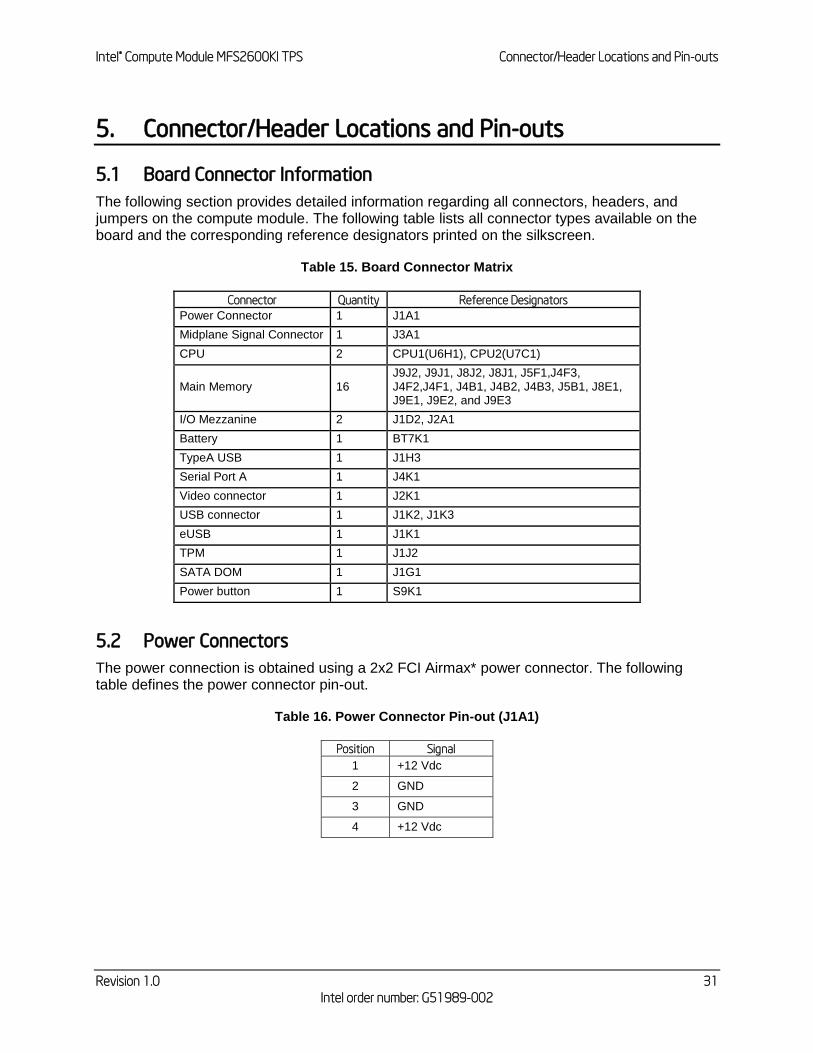
5. Connector/Header Locations and Pin-outs
5.1 Board Connector Information
The following section provides detailed information regarding all connectors, headers, and jumpers on the compute module. The following table lists all connector types available on the board and the corresponding reference designators printed on the silkscreen.
Table 15. Board Connector Matrix
Connector Quantity Reference Designators
Power Connector 1 J1A1
Midplane Signal Connector 1 J3A1
CPU 2 CPU1(U6H1), CPU2(U7C1)
Main Memory 16 J9J2, J9J1, J8J2, J8J1, J5F1,J4F3, J4F2,J4F1, J4B1, J4B2, J4B3, J5B1, J8E1, J9E1, J9E2, and J9E3
I/O Mezzanine 2 J1D2, J2A1
Battery 1 BT7K1
TypeA USB 1 J1H3
Serial Port A 1 J4K1
Video connector 1 J2K1
USB connector 1 J1K2, J1K3
eUSB 1 J1K1
TPM 1 J1J2
SATA DOM 1 J1G1
Power button 1 S9K1
5.2 Power Connectors
The power connection is obtained using a 2x2 FCI Airmax* power connector. The following table defines the power connector pin-out.
Table 16. Power Connector Pin-out (J1A1)
Position Signal
1 +12 Vdc
2 GND
3 GND
4 +12 Vdc
Connector/Header Locations and Pin-outs Intel® Compute Module MFS2600KI TPS
Revision 1.0
Intel order number: G51989-002
32
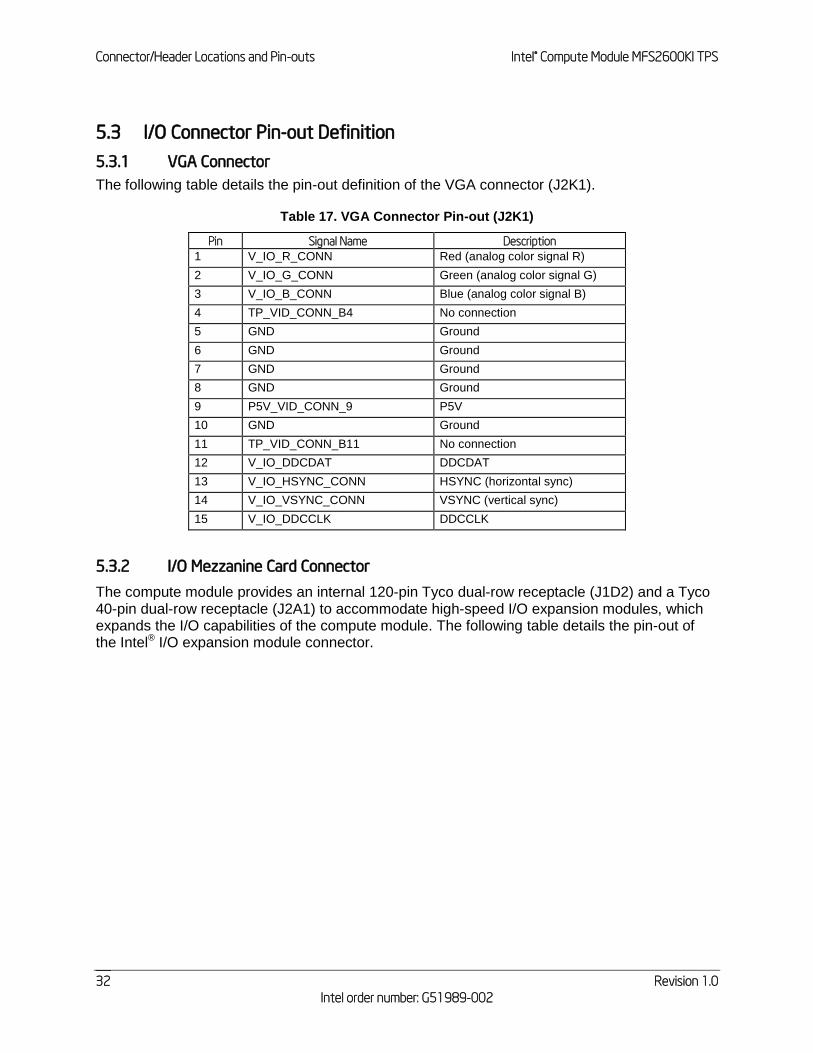
5.3 I/O Connector Pin-out Definition
5.3.1 VGA Connector
The following table details the pin-out definition of the VGA connector (J2K1).
Table 17. VGA Connector Pin-out (J2K1)
Pin Signal Name Description
1 V_IO_R_CONN Red (analog color signal R)
2 V_IO_G_CONN Green (analog color signal G)
3 V_IO_B_CONN Blue (analog color signal B)
4 TP_VID_CONN_B4 No connection
5 GND Ground
6 GND Ground
7 GND Ground
8 GND Ground
9 P5V_VID_CONN_9 P5V
10 GND Ground
11 TP_VID_CONN_B11 No connection
12 V_IO_DDCDAT DDCDAT
13 V_IO_HSYNC_CONN HSYNC (horizontal sync)
14 V_IO_VSYNC_CONN VSYNC (vertical sync)
15 V_IO_DDCCLK DDCCLK
5.3.2 I/O Mezzanine Card Connector
The compute module provides an internal 120-pin Tyco dual-row receptacle (J1D2) and a Tyco 40-pin dual-row receptacle (J2A1) to accommodate high-speed I/O expansion modules, which expands the I/O capabilities of the compute module. The following table details the pin-out of the Intel® I/O expansion module connector.
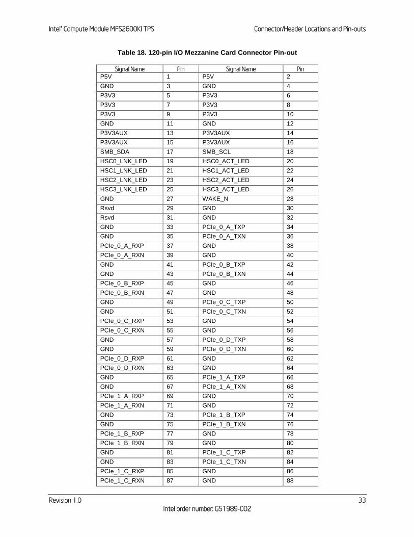
Intel® Compute Module MFS2600KI TPS Connector/Header Locations and Pin-outs
Revision 1.0 33
Intel order number: G51989-002
Table 18. 120-pin I/O Mezzanine Card Connector Pin-out
Signal Name Pin Signal Name Pin
P5V 1 P5V 2
GND 3 GND 4
P3V3 5 P3V3 6
P3V3 7 P3V3 8
P3V3 9 P3V3 10
GND 11 GND 12
P3V3AUX 13 P3V3AUX 14
P3V3AUX 15 P3V3AUX 16
SMB_SDA 17 SMB_SCL 18
HSC0_LNK_LED 19 HSC0_ACT_LED 20
HSC1_LNK_LED 21 HSC1_ACT_LED 22
HSC2_LNK_LED 23 HSC2_ACT_LED 24
HSC3_LNK_LED 25 HSC3_ACT_LED 26
GND 27 WAKE_N 28
Rsvd 29 GND 30
Rsvd 31 GND 32
GND 33 PCIe_0_A_TXP 34
GND 35 PCIe_0_A_TXN 36
PCIe_0_A_RXP 37 GND 38
PCIe_0_A_RXN 39 GND 40
GND 41 PCIe_0_B_TXP 42
GND 43 PCIe_0_B_TXN 44
PCIe_0_B_RXP 45 GND 46
PCIe_0_B_RXN 47 GND 48
GND 49 PCIe_0_C_TXP 50
GND 51 PCIe_0_C_TXN 52
PCIe_0_C_RXP 53 GND 54
PCIe_0_C_RXN 55 GND 56
GND 57 PCIe_0_D_TXP 58
GND 59 PCIe_0_D_TXN 60
PCIe_0_D_RXP 61 GND 62
PCIe_0_D_RXN 63 GND 64
GND 65 PCIe_1_A_TXP 66
GND 67 PCIe_1_A_TXN 68
PCIe_1_A_RXP 69 GND 70
PCIe_1_A_RXN 71 GND 72
GND 73 PCIe_1_B_TXP 74
GND 75 PCIe_1_B_TXN 76
PCIe_1_B_RXP 77 GND 78
PCIe_1_B_RXN 79 GND 80
GND 81 PCIe_1_C_TXP 82
GND 83 PCIe_1_C_TXN 84
PCIe_1_C_RXP 85 GND 86
PCIe_1_C_RXN 87 GND 88
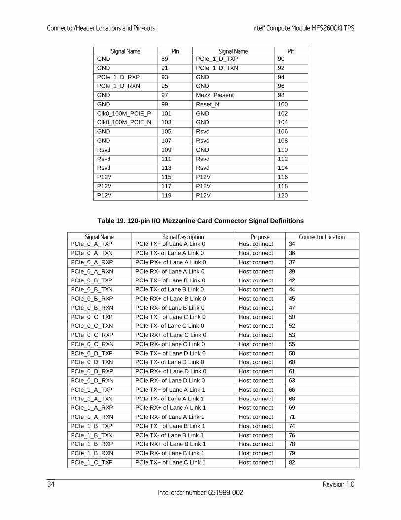
Connector/Header Locations and Pin-outs Intel® Compute Module MFS2600KI TPS
Revision 1.0
Intel order number: G51989-002
34
Signal Name Pin Signal Name Pin
GND 89 PCIe_1_D_TXP 90
GND 91 PCIe_1_D_TXN 92
PCIe_1_D_RXP 93 GND 94
PCIe_1_D_RXN 95 GND 96
GND 97 Mezz_Present 98
GND 99 Reset_N 100
Clk0_100M_PCIE_P 101 GND 102
Clk0_100M_PCIE_N 103 GND 104
GND 105 Rsvd 106
GND 107 Rsvd 108
Rsvd 109 GND 110
Rsvd 111 Rsvd 112
Rsvd 113 Rsvd 114
P12V 115 P12V 116
P12V 117 P12V 118
P12V 119 P12V 120
Table 19. 120-pin I/O Mezzanine Card Connector Signal Definitions
Signal Name Signal Description Purpose Connector Location
PCIe_0_A_TXP PCIe TX+ of Lane A Link 0 Host connect 34
PCIe_0_A_TXN PCIe TX- of Lane A Link 0 Host connect 36
PCIe_0_A_RXP PCIe RX+ of Lane A Link 0 Host connect 37
PCIe_0_A_RXN PCIe RX- of Lane A Link 0 Host connect 39
PCIe_0_B_TXP PCIe TX+ of Lane B Link 0 Host connect 42
PCIe_0_B_TXN PCIe TX- of Lane B Link 0 Host connect 44
PCIe_0_B_RXP PCIe RX+ of Lane B Link 0 Host connect 45
PCIe_0_B_RXN PCIe RX- of Lane B Link 0 Host connect 47
PCIe_0_C_TXP PCIe TX+ of Lane C Link 0 Host connect 50
PCIe_0_C_TXN PCIe TX- of Lane C Link 0 Host connect 52
PCIe_0_C_RXP PCIe RX+ of Lane C Link 0 Host connect 53
PCIe_0_C_RXN PCIe RX- of Lane C Link 0 Host connect 55
PCIe_0_D_TXP PCIe TX+ of Lane D Link 0 Host connect 58
PCIe_0_D_TXN PCIe TX- of Lane D Link 0 Host connect 60
PCIe_0_D_RXP PCIe RX+ of Lane D Link 0 Host connect 61
PCIe_0_D_RXN PCIe RX- of Lane D Link 0 Host connect 63
PCIe_1_A_TXP PCIe TX+ of Lane A Link 1 Host connect 66
PCIe_1_A_TXN PCIe TX- of Lane A Link 1 Host connect 68
PCIe_1_A_RXP PCIe RX+ of Lane A Link 1 Host connect 69
PCIe_1_A_RXN PCIe RX- of Lane A Link 1 Host connect 71
PCIe_1_B_TXP PCIe TX+ of Lane B Link 1 Host connect 74
PCIe_1_B_TXN PCIe TX- of Lane B Link 1 Host connect 76
PCIe_1_B_RXP PCIe RX+ of Lane B Link 1 Host connect 78
PCIe_1_B_RXN PCIe RX- of Lane B Link 1 Host connect 79
PCIe_1_C_TXP PCIe TX+ of Lane C Link 1 Host connect 82
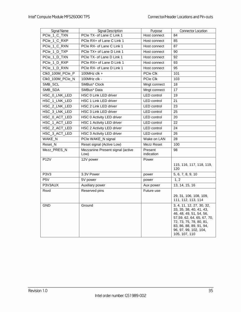
Intel® Compute Module MFS2600KI TPS Connector/Header Locations and Pin-outs
Revision 1.0 35
Intel order number: G51989-002
Signal Name Signal Description Purpose Connector Location
PCIe_1_C_TXN PCIe TX- of Lane C Link 1 Host connect 84
PCIe_1_C_RXP PCIe RX+ of Lane C Link 1 Host connect 85
PCIe_1_C_RXN PCIe RX- of Lane C Link 1 Host connect 87
PCIe_1_D_TXP PCIe TX+ of Lane D Link 1 Host connect 90
PCIe_1_D_TXN PCIe TX- of Lane D Link 1 Host connect 92
PCIe_1_D_RXP PCIe RX+ of Lane D Link 1 Host connect 93
PCIe_1_D_RXN PCIe RX- of Lane D Link 1 Host connect 95
Clk0_100M_PCIe_P 100MHz clk + PCIe Clk 101
Clk0_100M_PCIe_N 100MHz clk - PCIe Clk 103
SMB_SCL SMBus* Clock Mngt connect 18
SMB_SDA SMBus* Data Mngt connect 17
HSC_0_LNK_LED HSC 0 Link LED driver LED control 19
HSC_1_LNK_LED HSC 1 Link LED driver LED control 21
HSC_2_LNK_LED HSC 2 Link LED driver LED control 23
HSC_3_LNK_LED HSC 3 Link LED driver LED control 25
HSC_0_ACT_LED HSC 0 Activity LED driver LED control 20
HSC_1_ACT_LED HSC 1 Activity LED driver LED control 22
HSC_2_ACT_LED HSC 2 Activity LED driver LED control 24
HSC_3_ACT_LED HSC 3 Activity LED driver LED control 26
WAKE_N PCIe WAKE_N signal Wake on LAN 28
Reset_N Reset signal (Active Low) Mezz Reset 100
Mezz_PRES_N Mezzanine Present signal (active Low)
Present indication
98
P12V 12V power Power
115, 116, 117, 118, 119, 120
P3V3 3.3V Power power 5, 6, 7, 8, 9, 10
P5V 5V power power 1, 2
P3V3AUX Auxiliary power Aux power 13, 14, 15, 16
Rsvd Reserved pins Future use
29, 31, 106, 108, 109, 111, 112, 113, 114
GND Ground 3, 4, 11, 12, 27, 30, 32, 33, 35, 38, 40, 41, 43, 46, 48, 49, 51, 54, 56, 57,59, 62, 64, 65, 67, 70, 72, 73, 75, 78, 80, 81, 83, 86, 88, 89, 91, 94, 96, 97, 99, 102, 104, 105, 107, 110
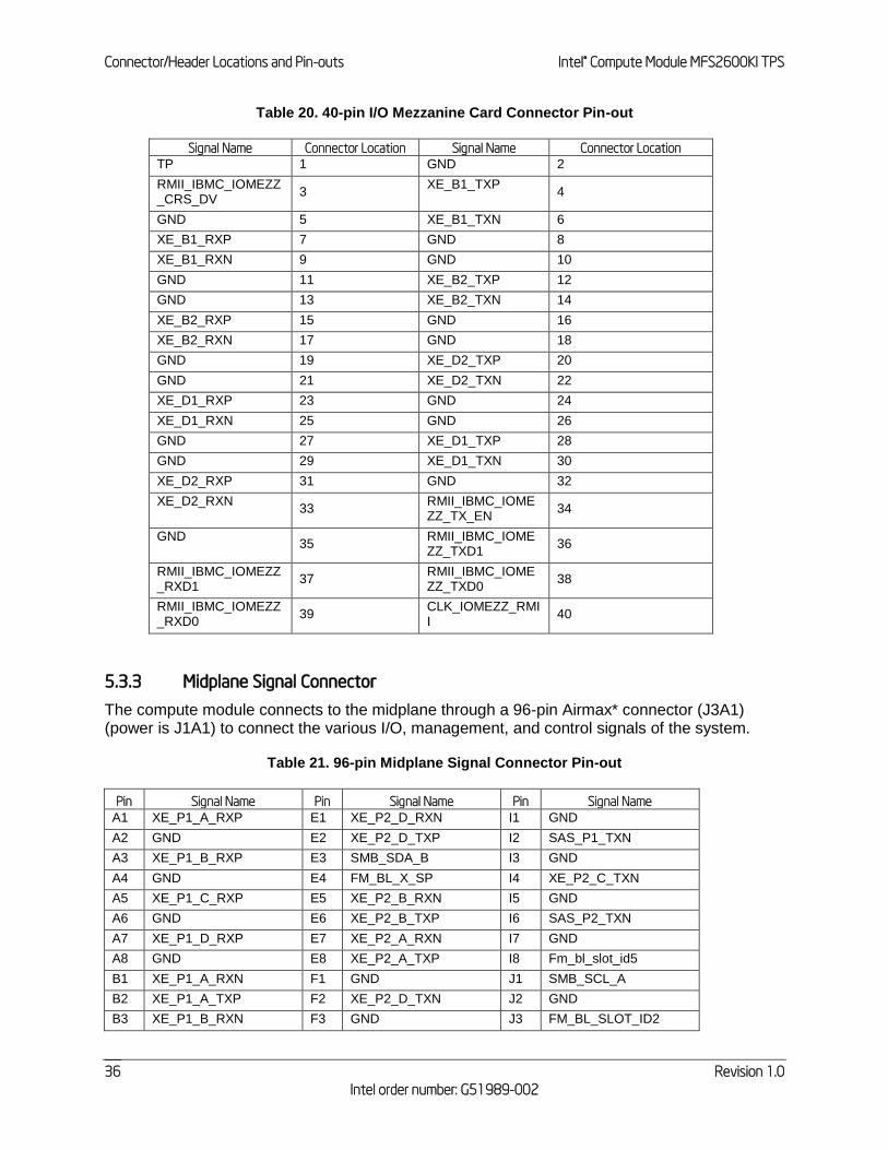
Connector/Header Locations and Pin-outs Intel® Compute Module MFS2600KI TPS
Revision 1.0
Intel order number: G51989-002
36
Table 20. 40-pin I/O Mezzanine Card Connector Pin-out
Signal Name Connector Location Signal Name Connector Location
TP 1 GND 2
RMII_IBMC_IOMEZZ_CRS_DV
3 XE_B1_TXP
4
GND 5 XE_B1_TXN 6
XE_B1_RXP 7 GND 8
XE_B1_RXN 9 GND 10
GND 11 XE_B2_TXP 12
GND 13 XE_B2_TXN 14
XE_B2_RXP 15 GND 16
XE_B2_RXN 17 GND 18
GND 19 XE_D2_TXP 20
GND 21 XE_D2_TXN 22
XE_D1_RXP 23 GND 24
XE_D1_RXN 25 GND 26
GND 27 XE_D1_TXP 28
GND 29 XE_D1_TXN 30
XE_D2_RXP 31 GND 32
XE_D2_RXN 33
RMII_IBMC_IOMEZZ_TX_EN
34
GND 35
RMII_IBMC_IOMEZZ_TXD1
36
RMII_IBMC_IOMEZZ_RXD1
37 RMII_IBMC_IOMEZZ_TXD0
38
RMII_IBMC_IOMEZZ_RXD0
39 CLK_IOMEZZ_RMII
40
5.3.3 Midplane Signal Connector
The compute module connects to the midplane through a 96-pin Airmax* connector (J3A1) (power is J1A1) to connect the various I/O, management, and control signals of the system.
Table 21. 96-pin Midplane Signal Connector Pin-out
Pin Signal Name Pin Signal Name Pin Signal Name
A1 XE_P1_A_RXP E1 XE_P2_D_RXN I1 GND
A2 GND E2 XE_P2_D_TXP I2 SAS_P1_TXN
A3 XE_P1_B_RXP E3 SMB_SDA_B I3 GND
A4 GND E4 FM_BL_X_SP I4 XE_P2_C_TXN
A5 XE_P1_C_RXP E5 XE_P2_B_RXN I5 GND
A6 GND E6 XE_P2_B_TXP I6 SAS_P2_TXN
A7 XE_P1_D_RXP E7 XE_P2_A_RXN I7 GND
A8 GND E8 XE_P2_A_TXP I8 Fm_bl_slot_id5
B1 XE_P1_A_RXN F1 GND J1 SMB_SCL_A
B2 XE_P1_A_TXP F2 XE_P2_D_TXN J2 GND
B3 XE_P1_B_RXN F3 GND J3 FM_BL_SLOT_ID2
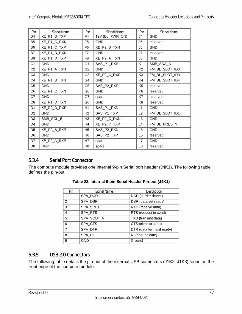
Intel® Compute Module MFS2600KI TPS Connector/Header Locations and Pin-outs
Revision 1.0 37
Intel order number: G51989-002
Pin Signal Name Pin Signal Name Pin Signal Name
B4 XE_P1_B_TXP F4 12V (BL_PWR_ON) J4 GND
B5 XE_P1_C_RXN F5 GND J5 reserved
B6 XE_P1_C_TXP F6 XE_P2_B_TXN J6 GND
B7 XE_P1_D_RXN F7 GND J7 reserved
B8 XE_P1_D_TXP F8 XE_P2_A_TXN J8 GND
C1 GND G1 SAS_P1_RXP K1 SMB_SDA_A
C2 XE_P1_A_TXN G2 GND K2 FM_BL_SLOT_ID0
C3 GND G3 XE_P2_C_RXP K3 FM_BL_SLOT_ID3
C4 XE_P1_B_TXN G4 GND K4 FM_BL_SLOT_ID4
C5 GND G5 SAS_P2_RXP K5 reserved
C6 XE_P1_C_TXN G6 GND K6 reserved
C7 GND G7 spare K7 reserved
C8 XE_P1_D_TXN G8 GND K8 reserved
D1 XE_P2_D_RXP H1 SAS_P1_RXN L1 GND
D2 GND H2 SAS_P1_TXP L2 FM_BL_SLOT_ID1
D3 SMB_SCL_B H3 XE_P2_C_RXN L3 GND
D4 GND H4 XE_P2_C_TXP L4 FM_BL_PRES_N
D5 XE_P2_B_RXP H5 SAS_P2_RXN L5 GND
D6 GND H6 SAS_P2_TXP L6 reserved
D7 XE_P2_A_RXP H7 spare L7 GND
D8 GND H8 spare L8 reserved
5.3.4 Serial Port Connector
The compute module provides one internal 9-pin Serial port header (J4K1). The following table defines the pin-out.
Table 22. Internal 9-pin Serial Header Pin-out (J4K1)
Pin Signal Name Description
1 SPA_DCD DCD (carrier detect)
2 SPA_DSR DSR (data set ready)
3 SPA_SIN_L RXD (receive data)
4 SPA_RTS RTS (request to send)
5 SPA_SOUT_N TXD (transmit data)
6 SPA_CTS CTS (clear to send)
7 SPA_DTR DTR (data terminal ready)
8 SPA_RI RI (ring Indicate)
9 GND Ground
5.3.5 USB 2.0 Connectors
The following table details the pin-out of the external USB connectors (J1K2, J1K3) found on the front edge of the compute module.
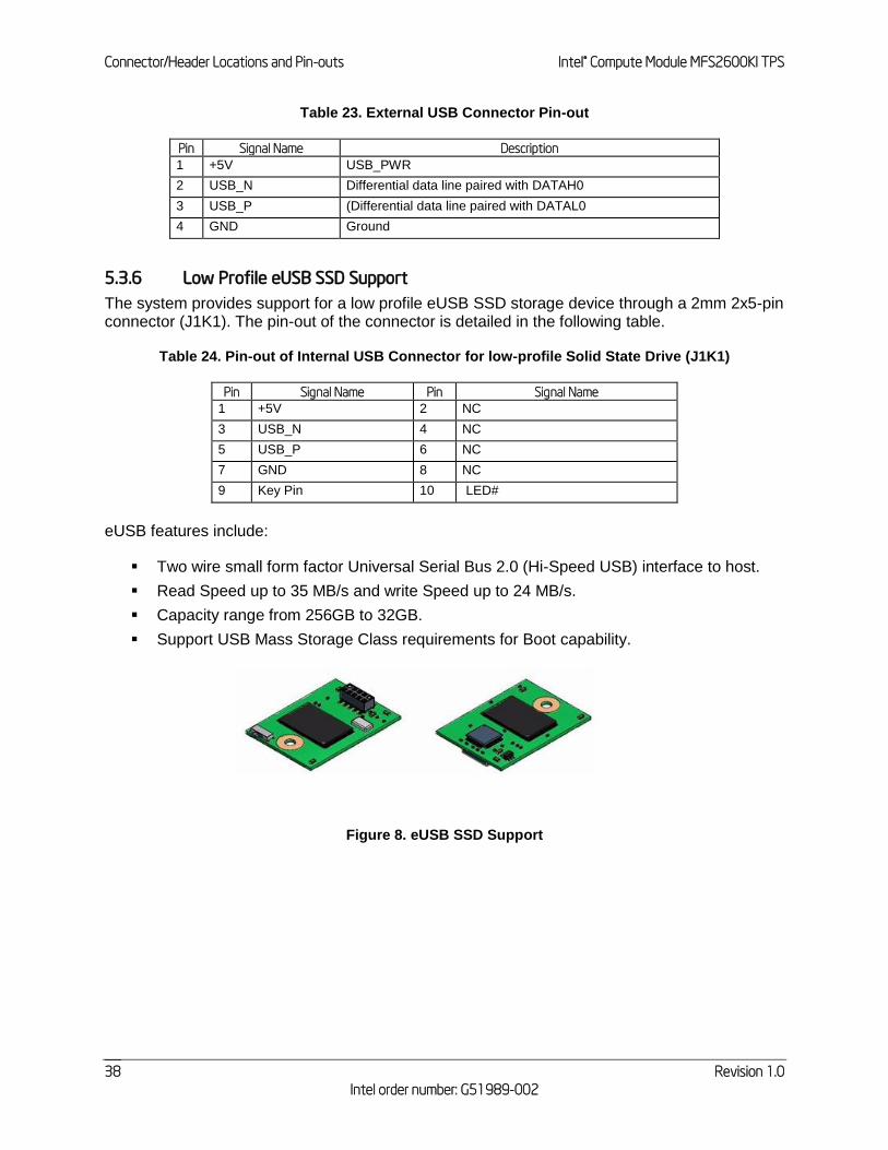
Connector/Header Locations and Pin-outs Intel® Compute Module MFS2600KI TPS
Revision 1.0
Intel order number: G51989-002
38
Table 23. External USB Connector Pin-out
Pin Signal Name Description
1 +5V USB_PWR
2 USB_N Differential data line paired with DATAH0
3 USB_P (Differential data line paired with DATAL0
4 GND Ground
5.3.6 Low Profile eUSB SSD Support
The system provides support for a low profile eUSB SSD storage device through a 2mm 2x5-pin connector (J1K1). The pin-out of the connector is detailed in the following table.
Table 24. Pin-out of Internal USB Connector for low-profile Solid State Drive (J1K1)
Pin Signal Name Pin Signal Name
1 +5V 2 NC
3 USB_N 4 NC
5 USB_P 6 NC
7 GND 8 NC
9 Key Pin 10 LED#
eUSB features include:
Two wire small form factor Universal Serial Bus 2.0 (Hi-Speed USB) interface to host.
Read Speed up to 35 MB/s and write Speed up to 24 MB/s.
Capacity range from 256GB to 32GB.
Support USB Mass Storage Class requirements for Boot capability.
Figure 8. eUSB SSD Support
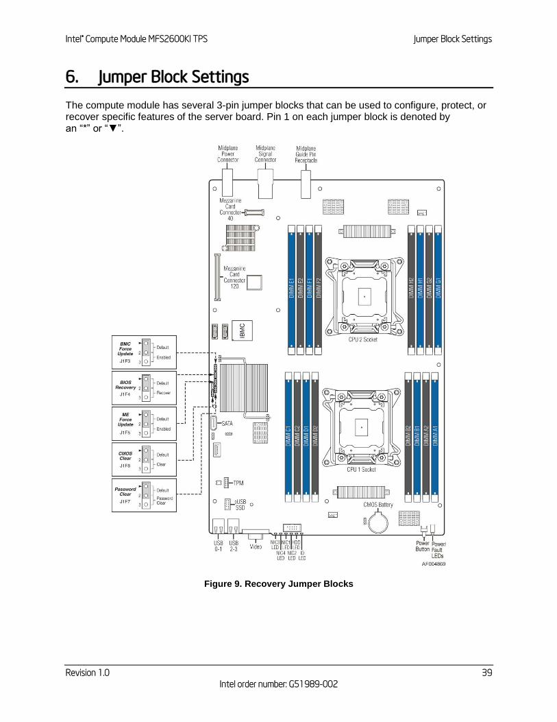
Intel® Compute Module MFS2600KI TPS Jumper Block Settings
Revision 1.0 39
Intel order number: G51989-002
6. Jumper Block Settings
The compute module has several 3-pin jumper blocks that can be used to configure, protect, or recover specific features of the server board. Pin 1 on each jumper block is denoted by an “*” or “▼”.
Figure 9. Recovery Jumper Blocks
Jumper Block Settings Intel® Compute Module MFS2600KI TPS
Revision 1.0
Intel order number: G51989-002
40
Table 25. Recovery Jumpers
Jumper Name Pins What happens at system reset …
J1F3: BMC Force
Update 1-2 BMC Firmware Force Update Mode – Disabled (Default)
2-3 BMC Firmware Force Update Mode – Enabled
J1F4: BIOS
R
e
c
o
v
e
r
1-2 These pins should have a jumper in place for normal operation. (Default)
2-3 If these pins are jumpered, the compute module boots from the emergency BIOS
image. These pins should not be jumpered for normal operation.
J1F5: ME Force
U
p
d
a
t
e
1-2 ME Firmware Force Update Mode – Disabled (Default)
2-3
ME Firmware Force Update Mode – Enabled
J1F8: CMOS Clear 1-2 These pins should have a jumper in place for normal operation. (Default)
2-3 If these pins are jumpered, the CMOS settings are cleared on the next boot. These
pins should not be jumpered for normal operation
J1F9: Password
C
l
e
a
r
1-2 These pins should have a jumper in place for normal operation. (Default)
2-3 To clear administrator and user passwords, power on the system with pins 2-3
connected. The administrator and user passwords clear in 5-10
seconds after power on. Pins 2-3 should not be connected for
normal system operation..
6.1 CMOS Clear and Password Clear Usage Procedure
The CMOS Clear (J1F8) and Password Clear (J1F9) recovery features are designed such that the desired operation can be achieved with minimal system downtime. The usage procedure for these two features has changed from previous generation Intel® server boards. The following procedure outlines the new usage model.
1. Power down the compute module.
2. Remove the compute module from the modular server chassis.
3. Open the compute module.
4. Move jumper from the default operating position (pins 1-2) to the Clear position (pins 2-3).
5. Wait 5 seconds.
6. Move jumper back to the default position (pins 1-2).
7. Close the compute module.
8. Reinstall the compute module in the modular server chassis.
9. Power up the compute module.
Intel® Compute Module MFS2600KI TPS Jumper Block Settings
Revision 1.0 41
Intel order number: G51989-002
Password and/or CMOS are now cleared and can be reset by going into the BIOS setup.
6.2 Integrated BMC Force Update Procedure
When performing a standard Integrated BMC firmware update procedure, the update utility places the Integrated BMC into an update mode, allowing the firmware to load safely onto the flash device. In the unlikely event that the Integrated BMC firmware update process fails due to the Integrated BMC not being in the proper update state, the compute module provides a BMC Force Update jumper (J1F3), which will force the Integrated BMC into the proper update state. The following procedure should be followed in the event the standard Integrated BMC firmware update process fails.
1. Power down the compute module.
2. Remove the compute module from the modular server chassis.
3. Open the compute module.
4. Move jumper from the default operating position (pins 1-2) to the “Enabled” position (pins 2-3)
5. Close the compute module.
6. Reinstall and power up the compute module.
7. Perform Integrated BMC firmware update procedure.
8. Power down the compute module.
9. Remove the compute module from the server system.
10. Move jumper from the “Enabled” position (pins 2-3) to the “Disabled” position (pins 1-2).
11. Close the compute module.
12. Reinstall the compute module into the modular server chassis.
13. Power up the compute module.
Note: Normal Integrated BMC functionality (for example, KVM, monitoring, and remote media) is disabled with the force BMC update jumper set to the “Enabled” position. The server should never be run with the BMC force update jumper set in this position and should only be used when the standard firmware update process fails. This jumper should remain in the default – disabled position when the server is running normally.
6.3 Integrated BMC Initialization
When the DC power is first applied to the compute module by installing it into a chassis, 5V-STBY is present, the Integrated BMC on the compute module requires 15-30 seconds to initialize. During this time, the power button functionality of the control panel is disabled, preventing the compute module from powering up.
6.4 ME Force Update Jumper
When performing the standard ME force update procedure, the update utility places the ME into an update mode, allowing the ME to load safely onto the flash device. In the unlikely event ME firmware update process fails due to ME not being in the proper update state, the compute module provides an Integrated BMC Force Update jumper, which forces the ME into the proper update state. The following procedure should be completed in the event the standard ME firmware update process fails.
Jumper Block Settings Intel® Compute Module MFS2600KI TPS
Revision 1.0
Intel order number: G51989-002
42
1. Power down and remove the compute module from chassis.
2. Open the compute module enclosure
3. Move jumper from the default operating position (covering pins 1 and 2) to the enabled position (covering pins 2 and 3).
4. Close the compute module enclosure.
5. Reinsert the compute module and power up.
6. Perform the ME firmware update procedure as documented in the README.TXT file that is included in the given ME firmware update package (same package as BIOS).
7. Power down and remove the compute module.
8. Open the compute module enclosure.
9. Move jumper from the enabled position (covering pins 2 and 3) to the disabled position (covering pins 1 and 2).
10. Close the compute module enclosure.
11. Reinsert the compute module and power up.
6.5 BIOS Recovery Jumper
The following procedure boots the recovery BIOS and flashes the normal BIOS:
1. Turn off the system power.
2. Move the BIOS recovery jumper to the recovery state.
3. Insert a bootable BIOS recovery media containing the new BIOS image files.
4. Turn on the system power.
The BIOS POST screen will appear displaying the progress, and the system will boot to the EFI shell. The EFI shell then executes the Startup.nsh batch file to start the flash update process. The user should then switch off the power and return the recovery jumper to its normal position. The user should not interrupt the BIOS POST on the first boot after recovery.
When the flash update completes:
1. Remove the recovery media.
2. Turn off the system power.
3. Restore the jumper to its original position.
4. Turn on the system power.
5. Re-flash any custom blocks, such as user binary or language blocks.
The system should now boot using the updated system BIOS.

Intel® Compute Module MFS2600KI TPS Product Regulatory Requirements
Revision 1.0 43
Intel order number: G51989-002
7. Product Regulatory Requirements
7.1 Product Regulatory Requirements
The Intel® Compute Module MFS2600KI is evaluated as part of the Intel® Modular Server System MFSYS25V2, which requires meeting all applicable system component regulatory requirements. Refer to the Intel® Modular Server System Technical Product Specification for a complete listing of all system and component regulatory requirements.
7.2 Product Regulatory Compliance and Safety Markings
No markings are required on the Intel® Compute Module MFS2600KI itself as it is evaluated as part of the Intel® Modular Server System MFSYS25V2.
7.3 Product Environmental/Ecology Requirements
The Intel® Compute Module MFS2600KI is evaluated as part of the Intel® Modular Server System MFSYS25V2, which requires meeting all applicable system component environmental and ecology requirements. For a complete listing of all system and component environment and ecology requirements and markings, refer to the Intel® Modular Server System Technical Product Specification.
Appendix A: Integration and Usage Tips Intel® Compute Module MFS2600KI TPS
Revision 1.0
Intel order number: G51989-002
44
Appendix A: Integration and Usage Tips
When two processors are installed, both must be of identical revision, core voltage, and bus/core speed. Mixed processor steppings are supported as long as they are listed in the processor specification updates published by Intel Corporation. However, the stepping of one processor cannot be greater than one stepping back of the other.
This server board supports The Intel® Xeon® Processor E5-2600 product family with a Thermal Design Power (TDP) of up to and including 95 Watts. Previous generations of the Intel® Xeon® processors are not supported.
Processors must be installed in order. CPU 1 must be populated for the Compute Module to operate.
On the front edge of the Compute Module are eight diagnostic LEDs that display a sequence of amber POST codes during the boot process. If the server board hangs during POST, the LEDs display the last POST event run before the hang.
This server board only supports registered DDR3 DIMMs (RDIMMs) and unbuffered DDR3 DIMMs (UDIMMs). Mixing of RDIMMs and UDIMMs is not supported.
For the best performance, the number of DDR3 DIMMs installed should be balanced across both processor sockets and memory channels. For example, a two-DIMM configuration performs better than a one-DIMM configuration. In a two-DIMM configuration, DIMMs should be installed in DIMM sockets A1 and E1. An eight-DIMM configuration (DIMM sockets A1, B1, C1, D1, E1, F1, G1, and H1) performs better than a four-DIMM configuration (DIMM sockets A1, B1, C1, and D1).
Normal Integrated BMC functionality (for example, KVM, monitoring, and remote media) is disabled with the BMC Force Update jumper set to the “enabled” position (pins 2-3). The Compute Module should never be run with the BMC Force Update jumper set in this position and should only be used when the standard firmware update process fails. This jumper should remain in the default (disabled) position (pins 1-2) when the server is running normally.
When performing a normal BIOS update procedure, the BIOS recovery jumper must be set to its default position (pins 1-2).
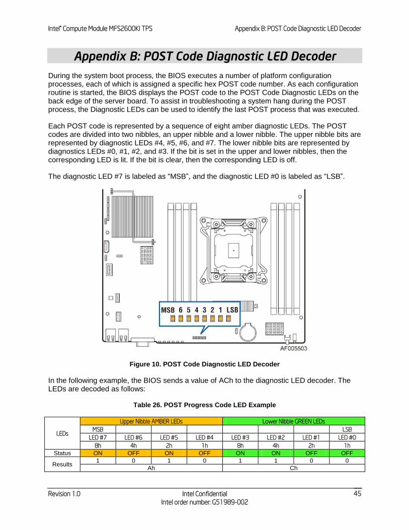
Intel® Compute Module MFS2600KI TPS Appendix B: POST Code Diagnostic LED Decoder
Revision 1.0 Intel Confidential
Intel order number: G51989-002
45
Appendix B: POST Code Diagnostic LED Decoder
During the system boot process, the BIOS executes a number of platform configuration processes, each of which is assigned a specific hex POST code number. As each configuration routine is started, the BIOS displays the POST code to the POST Code Diagnostic LEDs on the back edge of the server board. To assist in troubleshooting a system hang during the POST process, the Diagnostic LEDs can be used to identify the last POST process that was executed.
Each POST code is represented by a sequence of eight amber diagnostic LEDs. The POST codes are divided into two nibbles, an upper nibble and a lower nibble. The upper nibble bits are represented by diagnostic LEDs #4, #5, #6, and #7. The lower nibble bits are represented by diagnostics LEDs #0, #1, #2, and #3. If the bit is set in the upper and lower nibbles, then the corresponding LED is lit. If the bit is clear, then the corresponding LED is off.
The diagnostic LED #7 is labeled as “MSB”, and the diagnostic LED #0 is labeled as “LSB”.
Figure 10. POST Code Diagnostic LED Decoder
In the following example, the BIOS sends a value of ACh to the diagnostic LED decoder. The LEDs are decoded as follows:
Table 26. POST Progress Code LED Example
LEDs
Upper Nibble AMBER LEDs Lower Nibble GREEN LEDs MSB LSB
LED #7 LED #6 LED #5 LED #4 LED #3 LED #2 LED #1 LED #0
8h 4h 2h 1h 8h 4h 2h 1h
Status ON OFF ON OFF ON ON OFF OFF
Results 1 0 1 0 1 1 0 0
Ah Ch
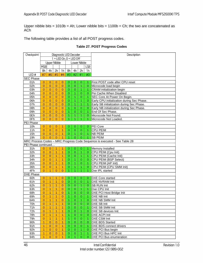
Appendix B: POST Code Diagnostic LED Decoder Intel® Compute Module MFS2600KI TPS
Intel Confidential Revision 1.0
Intel order number: G51989-002
46
Upper nibble bits = 1010b = Ah; Lower nibble bits = 1100b = Ch; the two are concatenated as ACh The following table provides a list of all POST progress codes.
Table 27. POST Progress Codes
Checkpoint Diagnostic LED Decoder Description
1 = LED On, 0 = LED Off
Upper Nibble Lower Nibble
MSB LSB
8h 4h 2h 1h 8h 4h 2h 1h
LED # #7 #6 #5 #4 #3 #2 #1 #0 SEC Phase
01h 0 0 0 0 0 0 0 1 First POST code after CPU reset
02h 0 0 0 0 0 0 1 0 Microcode load begin
03h 0 0 0 0 0 0 1 1 CRAM initialization begin
04h 0 0 0 0 0 1 0 0 Pei Cache When Disabled
05h 0 0 0 0 0 1 0 1 SEC Core At Power On Begin.
06h 0 0 0 0 0 1 1 0 Early CPU initialization during Sec Phase.
07h 0 0 0 0 0 1 1 1 Early SB initialization during Sec Phase.
08h 0 0 0 0 1 0 0 0 Early NB initialization during Sec Phase.
09h 0 0 0 0 1 0 0 1 End Of Sec Phase.
0Eh 0 0 0 0 1 1 1 0 Microcode Not Found.
0Fh 0 0 0 0 1 1 1 1 Microcode Not Loaded.
PEI Phase
10h 0 0 0 1 0 0 0 0 PEI Core
11h 0 0 0 1 0 0 0 1 CPU PEIM
15h 0 0 0 1 0 1 0 1 NB PEIM
19h 0 0 0 1 1 0 0 1 SB PEIM
MRC Process Codes – MRC Progress Code Sequence is executed - See Table 28
PEI Phase continued…
31h 0 0 1 1 0 0 0 1 Memory Installed
32h 0 0 1 1 0 0 1 0 CPU PEIM (Cpu Init)
33h 0 0 1 1 0 0 1 1 CPU PEIM (Cache Init)
34h 0 0 1 1 0 1 0 0 CPU PEIM (BSP Select)
35h 0 0 1 1 0 1 0 1 CPU PEIM (AP Init)
36h 0 0 1 1 0 1 1 0 CPU PEIM (CPU SMM Init)
4Fh 0 1 0 0 1 1 1 1 Dxe IPL started
DXE Phase
60h 0 1 1 0 0 0 0 0 DXE Core started
61h 0 1 1 0 0 0 0 1 DXE NVRAM Init
62h 0 1 1 0 0 0 1 0 SB RUN Init
63h 0 1 1 0 0 0 1 1 Dxe CPU Init
68h 0 1 1 0 1 0 0 0 DXE PCI Host Bridge Init
69h 0 1 1 0 1 0 0 1 DXE NB Init
6Ah 0 1 1 0 1 0 1 0 DXE NB SMM Init
70h 0 1 1 1 0 0 0 0 DXE SB Init
71h 0 1 1 1 0 0 0 1 DXE SB SMM Init
72h 0 1 1 1 0 0 1 0 DXE SB devices Init
78h 0 1 1 1 1 0 0 0 DXE ACPI Init
79h 0 1 1 1 1 0 0 1 DXE CSM Init
90h 1 0 0 1 0 0 0 0 DXE BDS Started
91h 1 0 0 1 0 0 0 1 DXE BDS connect drivers
92h 1 0 0 1 0 0 1 0 DXE PCI Bus begin
93h 1 0 0 1 0 0 1 1 DXE PCI Bus HPC Init
94h 1 0 0 1 0 1 0 0 DXE PCI Bus enumeration
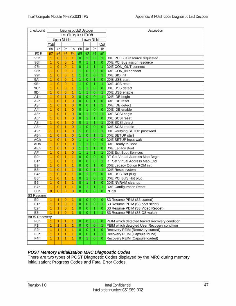
Intel® Compute Module MFS2600KI TPS Appendix B: POST Code Diagnostic LED Decoder
Revision 1.0 Intel Confidential
Intel order number: G51989-002
47
Checkpoint Diagnostic LED Decoder Description
1 = LED On, 0 = LED Off
Upper Nibble Lower Nibble
MSB LSB
8h 4h 2h 1h 8h 4h 2h 1h
LED # #7 #6 #5 #4 #3 #2 #1 #0 95h 1 0 0 1 0 1 0 1 DXE PCI Bus resource requested
96h 1 0 0 1 0 1 1 0 DXE PCI Bus assign resource
97h 1 0 0 1 0 1 1 1 DXE CON_OUT connect
98h 1 0 0 1 1 0 0 0 DXE CON_IN connect
99h 1 0 0 1 1 0 0 1 DXE SIO Init
9Ah 1 0 0 1 1 0 1 0 DXE USB start
9Bh 1 0 0 1 1 0 1 1 DXE USB reset
9Ch 1 0 0 1 1 1 0 0 DXE USB detect
9Dh 1 0 0 1 1 1 0 1 DXE USB enable
A1h 1 0 1 0 0 0 0 1 DXE IDE begin
A2h 1 0 1 0 0 0 1 0 DXE IDE reset
A3h 1 0 1 0 0 0 1 1 DXE IDE detect
A4h 1 0 1 0 0 1 0 0 DXE IDE enable
A5h 1 0 1 0 0 1 0 1 DXE SCSI begin
A6h 1 0 1 0 0 1 1 0 DXE SCSI reset
A7h 1 0 1 0 0 1 1 1 DXE SCSI detect
A8h 1 0 1 0 1 0 0 0 DXE SCSI enable
A9h 1 0 1 0 1 0 0 1 DXE verifying SETUP password
ABh 1 0 1 0 1 0 1 1 DXE SETUP start
ACh 1 0 1 0 1 1 0 0 DXE SETUP input wait
ADh 1 0 1 0 1 1 0 1 DXE Ready to Boot
AEh 1 0 1 0 1 1 1 0 DXE Legacy Boot
AFh 1 0 1 0 1 1 1 1 DXE Exit Boot Services
B0h 1 0 1 1 0 0 0 0 RT Set Virtual Address Map Begin
B1h 1 0 1 1 0 0 0 1 RT Set Virtual Address Map End
B2h 1 0 1 1 0 0 1 0 DXE Legacy Option ROM init
B3h 1 0 1 1 0 0 1 1 DXE Reset system
B4h 1 0 1 1 0 1 0 0 DXE USB Hot plug
B5h 1 0 1 1 0 1 0 1 DXE PCI BUS Hot plug
B6h 1 0 1 1 0 1 1 0 DXE NVRAM cleanup
B7h 1 0 1 1 0 1 1 1 DXE Configuration Reset
00h 0 0 0 0 0 0 0 0 INT19
S3 Resume
E0h 1 1 0 1 0 0 0 0 S3 Resume PEIM (S3 started)
E1h 1 1 0 1 0 0 0 1 S3 Resume PEIM (S3 boot script)
E2h 1 1 0 1 0 0 1 0 S3 Resume PEIM (S3 Video Repost)
E3h 1 1 0 1 0 0 1 1 S3 Resume PEIM (S3 OS wake)
BIOS Recovery
F0h 1 1 1 1 0 0 0 0 PEIM which detected forced Recovery condition
F1h 1 1 1 1 0 0 0 1 PEIM which detected User Recovery condition
F2h 1 1 1 1 0 0 1 0 Recovery PEIM (Recovery started)
F3h 1 1 1 1 0 0 1 1 Recovery PEIM (Capsule found)
F4h 1 1 1 1 0 1 0 0 Recovery PEIM (Capsule loaded)
POST Memory Initialization MRC Diagnostic Codes There are two types of POST Diagnostic Codes displayed by the MRC during memory initialization; Progress Codes and Fatal Error Codes.
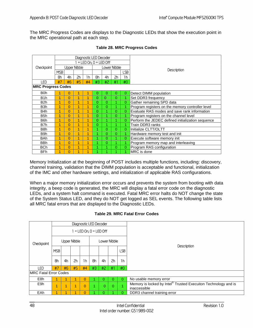
Appendix B: POST Code Diagnostic LED Decoder Intel® Compute Module MFS2600KI TPS
Intel Confidential Revision 1.0
Intel order number: G51989-002
48
The MRC Progress Codes are displays to the Diagnostic LEDs that show the execution point in the MRC operational path at each step.
Table 28. MRC Progress Codes
Checkpoint
Diagnostic LED Decoder
Description
1 = LED On, 0 = LED Off
Upper Nibble Lower Nibble
MSB LSB
8h 4h 2h 1h 8h 4h 2h 1h
LED #7 #6 #5 #4 #3 #2 #1 #0 MRC Progress Codes
B0h 1 0 1 1 0 0 0 0 Detect DIMM population
B1h 1 0 1 1 0 0 0 1 Set DDR3 frequency
B2h 1 0 1 1 0 0 1 0 Gather remaining SPD data
B3h 1 0 1 1 0 0 1 1 Program registers on the memory controller level
B4h 1 0 1 1 0 1 0 0 Evaluate RAS modes and save rank information
B5h 1 0 1 1 0 1 0 1 Program registers on the channel level
B6h 1 0 1 1 0 1 1 0 Perform the JEDEC defined initialization sequence
B7h 1 0 1 1 0 1 1 1 Train DDR3 ranks
B8h 1 0 1 1 1 0 0 0 Initialize CLTT/OLTT
B9h 1 0 1 1 1 0 0 1 Hardware memory test and init
BAh 1 0 1 1 1 0 1 0 Execute software memory init
BBh 1 0 1 1 1 0 1 1 Program memory map and interleaving
BCh 1 0 1 1 1 1 0 0 Program RAS configuration
BFh 1 0 1 1 1 1 1 1 MRC is done
Memory Initialization at the beginning of POST includes multiple functions, including: discovery, channel training, validation that the DIMM population is acceptable and functional, initialization of the IMC and other hardware settings, and initialization of applicable RAS configurations. When a major memory initialization error occurs and prevents the system from booting with data integrity, a beep code is generated, the MRC will display a fatal error code on the diagnostic LEDs, and a system halt command is executed. Fatal MRC error halts do NOT change the state of the System Status LED, and they do NOT get logged as SEL events. The following table lists all MRC fatal errors that are displayed to the Diagnostic LEDs.
Table 29. MRC Fatal Error Codes
Checkpoint
Diagnostic LED Decoder
Description
1 = LED On, 0 = LED Off
Upper Nibble Lower Nibble
MSB LSB
8h 4h 2h 1h 8h 4h 2h 1h
LED #7 #6 #5 #4 #3 #2 #1 #0
MRC Fatal Error Codes
E8h 1 1 1 0 1 0 0 0 No usable memory error
E9h 1 1 1 0 1 0 0 1
Memory is locked by Intel® Trusted Execuiton Technology and is
inaccessible
EAh 1 1 1 0 1 0 1 0 DDR3 channel training error
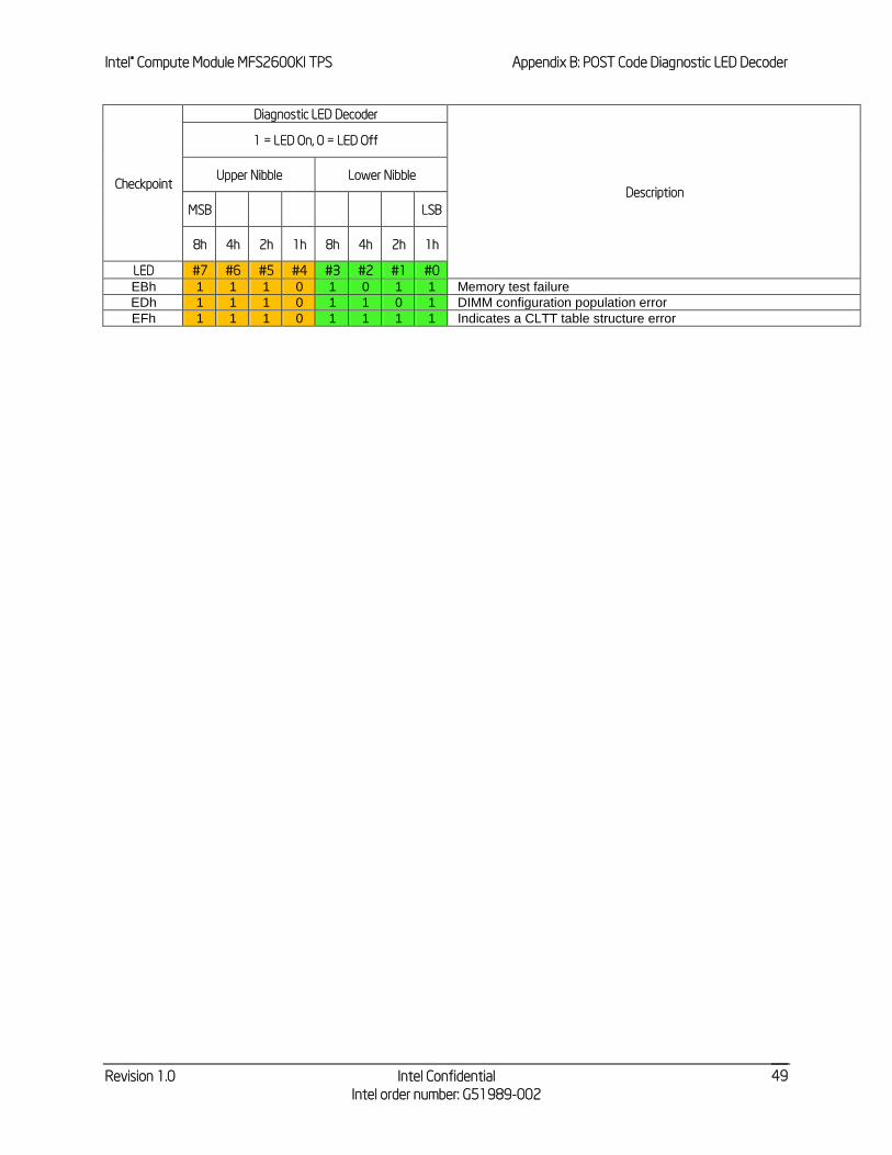
Intel® Compute Module MFS2600KI TPS Appendix B: POST Code Diagnostic LED Decoder
Revision 1.0 Intel Confidential
Intel order number: G51989-002
49
Checkpoint
Diagnostic LED Decoder
Description
1 = LED On, 0 = LED Off
Upper Nibble Lower Nibble
MSB LSB
8h 4h 2h 1h 8h 4h 2h 1h
LED #7 #6 #5 #4 #3 #2 #1 #0
EBh 1 1 1 0 1 0 1 1 Memory test failure
EDh 1 1 1 0 1 1 0 1 DIMM configuration population error
EFh 1 1 1 0 1 1 1 1 Indicates a CLTT table structure error

Appendix C: POST Error Code Intel® Compute Module MFS2600KI TPS
Intel Confidential Revision 1.0
Intel order number: G51989-002
50
Appendix C: POST Error Code
Most error conditions encountered during POST are reported using POST Error Codes. These codes represent specific failures, warnings, or informational messages that are identified with particular hardware units. These POST Error Codes may be displayed in the Error Manager display screen, and are always automatically logged to the System Event Log (SEL). The table below lists the supported POST Error Codes, with a descriptive Error Message text. For each, There is also a Response listed, which classifies the error as Minor, Major, or Fatal depending on how serious the error is and what action the system should take. The Response section in the following table indicates one of these actions:
Minor: The message is displayed on the screen or on the Error Manager screen, and an error is logged to the SEL. The system continues booting in a degraded state. The user may want to replace the erroneous unit. The POST Error Pause option setting in the BIOS setup does not have any effect on this error.
Major: The message is displayed on the Error Manager screen, and an error is logged to the SEL. The POST Error Pause option setting in the BIOS setup determines whether the system pauses to the Error Manager for this type of error so the user can take immediate corrective action or the system continues booting.
Fatal: The system halts during post at a blank screen with the text “Unrecoverable fatal error found. System will not boot until the error is resolved” and “Press <F2> to enter setup” The POST Error Pause option setting in the BIOS setup does not have any effect with this class of error.
Table 30. POST Error Codes and Messages
Error Code Error Message Response
0012 System RTC date/time not set Major
0048 Password check failed Major
0140 PCI component encountered a PERR error Major
0141 PCI resource conflict Major
0146 PCI out of resources error Major
0191 Processor core/thread count mismatch detected Fatal
0192 Processor cache size mismatch detected Fatal
0194 Processor family mismatch detected Fatal
0195 Processor Intel® QPI link frequencies unable to synchronize Fatal
0196 Processor model mismatch detected Fatal
0197 Processor frequencies unable to synchronize Fatal
5220 BIOS Settings reset to default settings Major
5221 Passwords cleared by jumper Major
5224 Password clear jumper is Set Major
8130 Processor 01 disabled Major
8131 Processor 02 disabled Major
8132 Processor 03 disabled Major
8133 Processor 04 disabled Major
8160 Processor 01 unable to apply microcode update Major
8161 Processor 02 unable to apply microcode update Major
8162 Processor 03 unable to apply microcode update Major
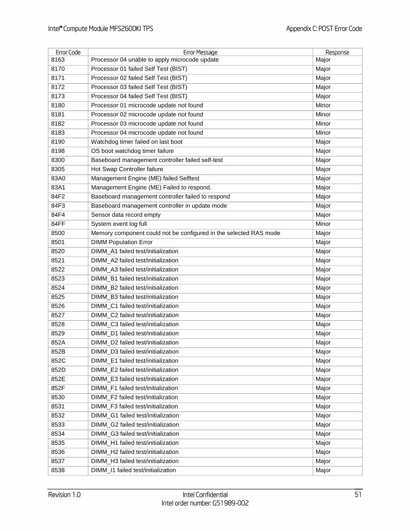
Intel® Compute Module MFS2600KI TPS Appendix C: POST Error Code
Revision 1.0 Intel Confidential
Intel order number: G51989-002
51
Error Code Error Message Response
8163 Processor 04 unable to apply microcode update Major
8170 Processor 01 failed Self Test (BIST) Major
8171 Processor 02 failed Self Test (BIST) Major
8172 Processor 03 failed Self Test (BIST) Major
8173 Processor 04 failed Self Test (BIST) Major
8180 Processor 01 microcode update not found Minor
8181 Processor 02 microcode update not found Minor
8182 Processor 03 microcode update not found Minor
8183 Processor 04 microcode update not found Minor
8190 Watchdog timer failed on last boot Major
8198 OS boot watchdog timer failure Major
8300 Baseboard management controller failed self-test Major
8305 Hot Swap Controller failure Major
83A0 Management Engine (ME) failed Selftest Major
83A1 Management Engine (ME) Failed to respond. Major
84F2 Baseboard management controller failed to respond Major
84F3 Baseboard management controller in update mode Major
84F4 Sensor data record empty Major
84FF System event log full Minor
8500 Memory component could not be configured in the selected RAS mode Major
8501 DIMM Population Error Major
8520 DIMM_A1 failed test/initialization Major
8521 DIMM_A2 failed test/initialization Major
8522 DIMM_A3 failed test/initialization Major
8523 DIMM_B1 failed test/initialization Major
8524 DIMM_B2 failed test/initialization Major
8525 DIMM_B3 failed test/initialization Major
8526 DIMM_C1 failed test/initialization Major
8527 DIMM_C2 failed test/initialization Major
8528 DIMM_C3 failed test/initialization Major
8529 DIMM_D1 failed test/initialization Major
852A DIMM_D2 failed test/initialization Major
852B DIMM_D3 failed test/initialization Major
852C DIMM_E1 failed test/initialization Major
852D DIMM_E2 failed test/initialization Major
852E DIMM_E3 failed test/initialization Major
852F DIMM_F1 failed test/initialization Major
8530 DIMM_F2 failed test/initialization Major
8531 DIMM_F3 failed test/initialization Major
8532 DIMM_G1 failed test/initialization Major
8533 DIMM_G2 failed test/initialization Major
8534 DIMM_G3 failed test/initialization Major
8535 DIMM_H1 failed test/initialization Major
8536 DIMM_H2 failed test/initialization Major
8537 DIMM_H3 failed test/initialization Major
8538 DIMM_I1 failed test/initialization Major
Appendix C: POST Error Code Intel® Compute Module MFS2600KI TPS
Intel Confidential Revision 1.0
Intel order number: G51989-002
52
Error Code Error Message Response
8539 DIMM_I2 failed test/initialization Major
853A DIMM_I3 failed test/initialization Major
853B DIMM_J1 failed test/initialization Major
853C DIMM_J2 failed test/initialization Major
853D DIMM_J3 failed test/initialization Major
853E DIMM_K1 failed test/initialization Major
853F (Go to 85C0)
DIMM_K2 failed test/initialization Major
8540 DIMM_A1 disabled Major
8541 DIMM_A2 disabled Major
8542 DIMM_A3 disabled Major
8543 DIMM_B1 disabled Major
8544 DIMM_B2 disabled Major
8545 DIMM_B3 disabled Major
8546 DIMM_C1 disabled Major
8547 DIMM_C2 disabled Major
8548 DIMM_C3 disabled Major
8549 DIMM_D1 disabled Major
854A DIMM_D2 disabled Major
854B DIMM_D3 disabled Major
854C DIMM_E1 disabled Major
854D DIMM_E2 disabled Major
854E DIMM_E3 disabled Major
854F DIMM_F1 disabled Major
8550 DIMM_F2 disabled Major
8551 DIMM_F3 disabled Major
8552 DIMM_G1 disabled Major
8553 DIMM_G2 disabled Major
8554 DIMM_G3 disabled Major
8555 DIMM_H1 disabled Major
8556 DIMM_H2 disabled Major
8557 DIMM_H3 disabled Major
8558 DIMM_I1 disabled Major
8559 DIMM_I2 disabled Major
855A DIMM_I3 disabled Major
855B DIMM_J1 disabled Major
855C DIMM_J2 disabled Major
855D DIMM_J3 disabled Major
855E DIMM_K1 disabled Major
855F (Go to 85D0)
DIMM_K2 disabled Major
8560 DIMM_A1 encountered a Serial Presence Detection (SPD) failure Major
8561 DIMM_A2 encountered a Serial Presence Detection (SPD) failure Major
8562 DIMM_A3 encountered a Serial Presence Detection (SPD) failure Major
8563 DIMM_B1 encountered a Serial Presence Detection (SPD) failure Major
Intel® Compute Module MFS2600KI TPS Appendix C: POST Error Code
Revision 1.0 Intel Confidential
Intel order number: G51989-002
53
Error Code Error Message Response
8564 DIMM_B2 encountered a Serial Presence Detection (SPD) failure Major
8565 DIMM_B3 encountered a Serial Presence Detection (SPD) failure Major
8566 DIMM_C1 encountered a Serial Presence Detection (SPD) failure Major
8567 DIMM_C2 encountered a Serial Presence Detection (SPD) failure Major
8568 DIMM_C3 encountered a Serial Presence Detection (SPD) failure Major
8569 DIMM_D1 encountered a Serial Presence Detection (SPD) failure Major
856A DIMM_D2 encountered a Serial Presence Detection (SPD) failure Major
856B DIMM_D3 encountered a Serial Presence Detection (SPD) failure Major
856C DIMM_E1 encountered a Serial Presence Detection (SPD) failure Major
856D DIMM_E2 encountered a Serial Presence Detection (SPD) failure Major
856E DIMM_E3 encountered a Serial Presence Detection (SPD) failure Major
856F DIMM_F1 encountered a Serial Presence Detection (SPD) failure Major
8570 DIMM_F2 encountered a Serial Presence Detection (SPD) failure Major
8571 DIMM_F3 encountered a Serial Presence Detection (SPD) failure Major
8572 DIMM_G1 encountered a Serial Presence Detection (SPD) failure Major
8573 DIMM_G2 encountered a Serial Presence Detection (SPD) failure Major
8574 DIMM_G3 encountered a Serial Presence Detection (SPD) failure Major
8575 DIMM_H1 encountered a Serial Presence Detection (SPD) failure Major
8576 DIMM_H2 encountered a Serial Presence Detection (SPD) failure Major
8577 DIMM_H3 encountered a Serial Presence Detection (SPD) failure Major
8578 DIMM_I1 encountered a Serial Presence Detection (SPD) failure Major
8579 DIMM_I2 encountered a Serial Presence Detection (SPD) failure Major
857A DIMM_I3 encountered a Serial Presence Detection (SPD) failure Major
857B DIMM_J1 encountered a Serial Presence Detection (SPD) failure Major
857C DIMM_J2 encountered a Serial Presence Detection (SPD) failure Major
857D DIMM_J3 encountered a Serial Presence Detection (SPD) failure Major
857E DIMM_K1 encountered a Serial Presence Detection (SPD) failure Major
857F (Go to 85E0)
DIMM_K2 encountered a Serial Presence Detection (SPD) failure Major
85C0 DIMM_K3 failed test/initialization Major
85C1 DIMM_L1 failed test/initialization Major
85C2 DIMM_L2 failed test/initialization Major
85C3 DIMM_L3 failed test/initialization Major
85C4 DIMM_M1 failed test/initialization Major
85C5 DIMM_M2 failed test/initialization Major
85C6 DIMM_M3 failed test/initialization Major
85C7 DIMM_N1 failed test/initialization Major
85C8 DIMM_N2 failed test/initialization Major
85C9 DIMM_N3 failed test/initialization Major
85CA DIMM_O1 failed test/initialization Major
85CB DIMM_O2 failed test/initialization Major
85CC DIMM_O3 failed test/initialization Major
85CD DIMM_P1 failed test/initialization Major
85CE DIMM_P2 failed test/initialization Major
85CF DIMM_P3 failed test/initialization Major
Appendix C: POST Error Code Intel® Compute Module MFS2600KI TPS
Intel Confidential Revision 1.0
Intel order number: G51989-002
54
Error Code Error Message Response
85D0 DIMM_K3 disabled Major
85D1 DIMM_L1 disabled Major
85D2 DIMM_L2 disabled Major
85D3 DIMM_L3 disabled Major
85D4 DIMM_M1 disabled Major
85D5 DIMM_M2 disabled Major
85D6 DIMM_M3 disabled Major
85D7 DIMM_N1 disabled Major
85D8 DIMM_N2 disabled Major
85D9 DIMM_N3 disabled Major
85DA DIMM_O1 disabled Major
85DB DIMM_O2 disabled Major
85DC DIMM_O3 disabled Major
85DD DIMM_P1 disabled Major
85DE DIMM_P2 disabled Major
85DF DIMM_P3 disabled Major
85E0 DIMM_K3 encountered a Serial Presence Detection (SPD) failure Major
85E1 DIMM_L1 encountered a Serial Presence Detection (SPD) failure Major
85E2 DIMM_L2 encountered a Serial Presence Detection (SPD) failure Major
85E3 DIMM_L3 encountered a Serial Presence Detection (SPD) failure Major
85E4 DIMM_M1 encountered a Serial Presence Detection (SPD) failure Major
85E5 DIMM_M2 encountered a Serial Presence Detection (SPD) failure Major
85E6 DIMM_M3 encountered a Serial Presence Detection (SPD) failure Major
85E7 DIMM_N1 encountered a Serial Presence Detection (SPD) failure Major
85E8 DIMM_N2 encountered a Serial Presence Detection (SPD) failure Major
85E9 DIMM_N3 encountered a Serial Presence Detection (SPD) failure Major
85EA DIMM_O1 encountered a Serial Presence Detection (SPD) failure Major
85EB DIMM_O2 encountered a Serial Presence Detection (SPD) failure Major
85EC DIMM_O3 encountered a Serial Presence Detection (SPD) failure Major
85ED DIMM_P1 encountered a Serial Presence Detection (SPD) failure Major
85EE DIMM_P2 encountered a Serial Presence Detection (SPD) failure Major
85EF DIMM_P3 encountered a Serial Presence Detection (SPD) failure Major
8604 POST Reclaim of non-critical NVRAM variables Minor
8605 BIOS Settings are corrupted Major
92A3 Serial port component was not detected Major
92A9 Serial port component encountered a resource conflict error Major
A000 TPM device not detected. Minor
A001 TPM device missing or not responding. Minor
A002 TPM device failure. Minor
A003 TPM device failed self-test. Minor
A100 BIOS ACM Error Major
A421 PCI component encountered a SERR error Fatal
A5A0 PCI Express component encountered a PERR error Minor
A5A1 PCI Express component encountered an SERR error Fatal

Intel® Compute Module MFS2600KI TPS Appendix C: POST Error Code
Revision 1.0 Intel Confidential
Intel order number: G51989-002
55
The following table lists the POST error beep codes. Prior to system video initialization, the BIOS uses these beep codes to inform users on error conditions. The beep code is followed by a user-visible code on the POST Progress LEDs
Table 31. POST Error Beep Codes
Beeps Error Message POST Progress Code Description
3 Memory error See Table 64 System halted because a fatal error related to the memory
was detected.
1 long Intel® TXT security
violation
0xAE, 0xAF System halted because Intel® Trusted Execution
Technology detected a potential violation of system
security.
POST Error Beep Code The Integrated BMC may generate beep codes upon detection of failure conditions. Beep codes are sounded each time the problem is discovered, such as on each power-up attempt, but are not sounded continuously. Codes that are common across all Intel® server boards and systems that use same generation chipset are listed in the following table. Each digit in the code is represented by a sequence of beeps whose count is equal to the digit.
Table 32. Integrated BMC Beep Codes
Code Reason for Beep Associated Sensors
1-5-2-1 No CPUs installed or first CPU socket is
empty.
CPU Missing Sensor
1-5-2-4 MSID Mismatch. MSID Mismatch Sensor.
1-5-4-2 Power fault: DC power is unexpectedly
lost (power good
dropout).
Power unit – power unit failure
offset.
1-5-4-4 Power control fault (power good assertion
timeout).
Power unit – soft power control
failure
offset.
1-5-1-2 VR Watchdog Timer sensor assertion VR Watchdog Timer
1-5-1-4 The system does not power on or
unexpectedly
powers off and a
power supply unit
(PSU) is present
that is an
incompatible model
with one or more
other PSUs in the
system
PS Status
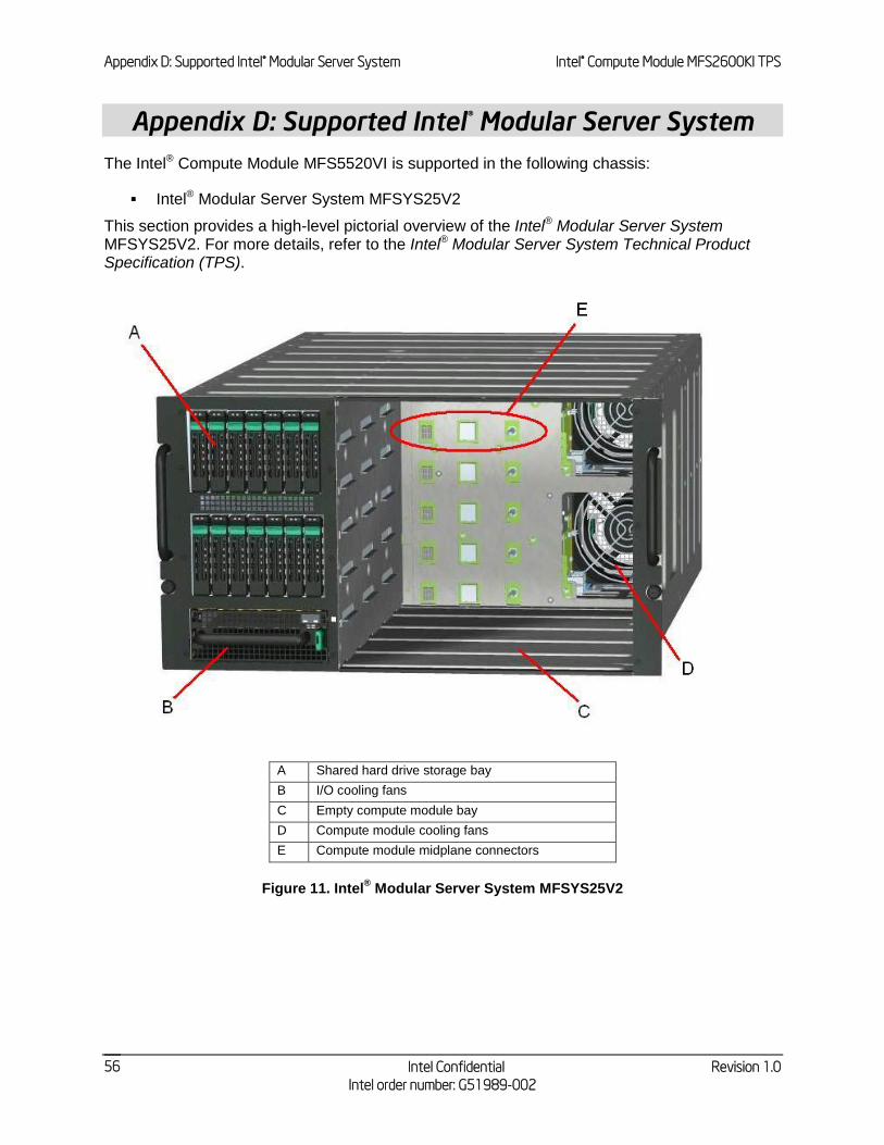
Appendix D: Supported Intel® Modular Server System Intel® Compute Module MFS2600KI TPS
Intel Confidential Revision 1.0
Intel order number: G51989-002
56
Appendix D: Supported Intel® Modular Server System
The Intel® Compute Module MFS5520VI is supported in the following chassis:
Intel® Modular Server System MFSYS25V2
This section provides a high-level pictorial overview of the Intel® Modular Server System MFSYS25V2. For more details, refer to the Intel® Modular Server System Technical Product Specification (TPS).
A Shared hard drive storage bay
B I/O cooling fans
C Empty compute module bay
D Compute module cooling fans
E Compute module midplane connectors
Figure 11. Intel® Modular Server System MFSYS25V2

Intel® Compute Module MFS2600KI TPS Glossary
Revision 1.0 Intel Confidential
Intel order number: G51989-002
57
Glossary
This appendix contains important terms used in the preceding chapters. For ease of use, numeric entries are listed first (for example, “82460GX”) followed by alpha entries (for example, “AGP 4x”). Acronyms are followed by non-acronyms.
Term Definition
ACPI Advanced Configuration and Power Interface
AP Application Processor
APIC Advanced Programmable Interrupt Control
ASIC Application Specific Integrated Circuit
ASMI Advanced Server Management Interface
BIOS Basic Input/Output System
BIST Built-In Self Test
BMC Baseboard Management Controller
Bridge Circuitry connecting one computer bus to another, allowing an agent on one to access the other
BSP Bootstrap Processor
byte 8-bit quantity.
CBC Chassis Bridge Controller (A microcontroller connected to one or more other CBCs, together they bridge the IPMB buses of multiple chassis.
CEK Common Enabling Kit
CHAP Challenge Handshake Authentication Protocol
CMOS In terms of this specification, this describes the PC-AT compatible region of battery-backed 128 bytes of memory, which normally resides on the server board.
DPC Direct Platform Control
EEPROM Electrically Erasable Programmable Read-Only Memory
EHCI Enhanced Host Controller Interface
EMP Emergency Management Port
EPS External Product Specification
ESB2 Enterprise South Bridge 2
FBD Fully Buffered DIMM
FMB Flexible Mother Board
FRB Fault Resilient Booting
FRU Field Replaceable Unit
FSB Front-Side Bus
GB 1024MB
GPIO General Purpose I/O
GTL Gunning Transceiver Logic
HSC Hot-Swap Controller
Hz Hertz (1 cycle/second)
I2C Inter-Integrated Circuit Bus
IA Intel® Architecture
IBF Input Buffer
ICH I/O Controller Hub
ICMB Intelligent Chassis Management Bus
IERR Internal Error

Glossary Intel® Compute Module MFS2600KI TPS
Intel Confidential Revision 1.0
Intel order number: G51989-002
58
Term Definition
IFB I/O and Firmware Bridge
INTR Interrupt
IP Internet Protocol
IPMB Intelligent Platform Management Bus
IPMI Intelligent Platform Management Interface
IR Infrared
ITP In-Target Probe
KB 1024 bytes
KCS Keyboard Controller Style
LAN Local Area Network
LCD Liquid Crystal Display
LED Light Emitting Diode
LPC Low Pin Count
LUN Logical Unit Number
MAC Media Access Control
MB 1024KB
MCH Memory Controller Hub
MD2 Message Digest 2 – Hashing Algorithm
MD5 Message Digest 5 – Hashing Algorithm – Higher Security
ms milliseconds
MTTR Memory Type Range Register
Mux Multiplexor
NIC Network Interface Controller
NMI Non-maskable Interrupt
OBF Output Buffer
OEM Original Equipment Manufacturer
Ohm Unit of electrical resistance
PEF Platform Event Filtering
PEP Platform Event Paging
PIA Platform Information Area (This feature configures the firmware for the platform hardware)
PLD Programmable Logic Device
PMI Platform Management Interrupt
POST Power-On Self Test
PSMI Power Supply Management Interface
PWM Pulse-Width Modulation
RAM Random Access Memory
RASUM Reliability, Availability, Serviceability, Usability, and Manageability
RISC Reduced Instruction Set Computing
ROM Read Only Memory
RTC Real-Time Clock (Component of ICH peripheral chip on the server board)
SDR Sensor Data Record
SECC Single Edge Connector Cartridge
SEEPROM Serial Electrically Erasable Programmable Read-Only Memory
SEL System Event Log
SIO Server Input/Output
Intel® Compute Module MFS2600KI TPS Glossary
Revision 1.0 Intel Confidential
Intel order number: G51989-002
59
Term Definition
SMBus* System Management Bus
SMI Server Management Interrupt (SMI is the highest priority non-maskable interrupt)
SMM Server Management Mode
SMS Server Management Software
SNMP Simple Network Management Protocol
TBD To Be Determined
TIM Thermal Interface Material
UART Universal Asynchronous Receiver/Transmitter
UDP User Datagram Protocol
UHCI Universal Host Controller Interface
UTC Universal time coordinate
VID Voltage Identification
VRD Voltage Regulator Down
Word 16-bit quantity
ZIF Zero Insertion Force
Reference Documents Intel® Compute Module MFS2600KI TPS
Intel Confidential Revision 1.0
Intel order number: G51989-002
60
Reference Documents
For additional information, refer to the Intel® Modular Server System Technical Product Specification.