Embed Size (px)
Citation preview

TELESCAN
Volume 6 - August 2017

We are much honoured and happy to present you ‘TELESCAN 2017’,
our Departmental Magazine. As TELESCAN is a technical magazine, it
provides a platform to the students to express their advanced technical
knowledge. Students get inspired to do study on latest technology before
submitting their articles. It is surely beneficial for students.
We would like to thanks Mrs M.P. Sardey (HOD), Mrs Harshada Magar
& Mrs G.D.Salunkhe for their support and encouraging us to represent such a
wonder. This year we have got good response from students and we have made
our best to make TELESCAN the gem.
Editorial Team: Staff Coordinator:
Sayyadusama Bijapuri (BE-C) Mrs.Harshada Magar
Tejaswini Muley (BE-C) Mrs.G.D. Salunkhe
Prachi Kolte (TE-A)
Saurav Kamble (TE-A)
Nikhil Bagad (TE-C)
VISION OF E&TC DEPARTMENT
• To provide quality education in electronics & telecommunication
engineering with professional ethics
MISSION OF E&TC DEPARTMENT
• To develop technical competency, ethics for professional growth and a sense of social responsibility among students

INDEX
SR NO. NAME PAGE NO.
1 NANO-TECHNOLOGY 1
2 LIGHT FIDELITY 3
3 CLOUD COMPUTING 5
4 HOW DOES GPS WORKS? 7
5 MORE THAN A VIEW-WINDOWS DOUBLE
AS A SOLAR PANEL
8
6 IGESTIBLE DEVICES THAT DRAW POWER
FROM STOMACH ACID
10
7 NEW THERMAL ABILITIES FOR SEMICONDUCTOR 12
8 ANALOGY BETWEEN IOT AND HUMAN BODY 13
9 BREATHABLE,WEARABLE MONITORING SKIN
FOR LONG TERM HEALTH MONITORING
15
10 2 -D ELECTRONICS 16
11 ORGANIC ELECTRONICS 18
12 MEMRISTOR 21
13 COLOUR SHIFTING SKIN THAT COULD HAVE WEARABLE
TECH AND PROSTHETIC USES
24
14 SPINTRONICS 26
15 STICKY INSECT SIZED DRONES TO POLLINATE CROPS 28


TELESCAN2017
Department of Electronics and Telecommunication Page 1
Nanotechnology
What is nanotechnology?
Nanotechnology is the design, characteristics, production and application of structures, devices and systems by
controlling shape and size at nanometric scale.
Nano science and nanotechnology are the study and application of extremely small things and can be used
across all the other science fields, such as chemistry, biology, physics, material science, and engineering.
How it started?
The ideas and concepts behind nanoscience and nanotechnology started with a talk entitled ―There‘s Plenty of
Room at the Bottom‖ by physicist Richard Feynman at an American Physical Society meeting at the California
Institute of Technology (Caltech) on December 29, 1959, long before the term nanotechnology was used. In his
talk, Feynman described a process in which scientists would be able to manipulate and control individual atoms
and molecules. Over a decade later, in his explorations of ultra precision machining, Professor Norio Taniguchi
coined the term nanotechnology. It wasn't until 1981, with the development of the scanning tunneling
microscope that could "see" individual atoms, which modern nanotechnology began.
What are the uses of nanotechnology?
Various types of detecting elements, such as carbon nanotubes, zinc oxide nanowires or
palladium nanoparticles can be used in nanotechnology-based sensors. Because of the small size of nanotubes,
nanowires, or nanoparticles, a few gas molecules are sufficient to change the electrical properties of the sensing
elements.
Nanotechnology in electronics
Nanoelectronics refers to the use of nanotechnology on electronic component especially transistors.
Nanoelectronics often refer to transistor devices that are small that inter-atomic interactions and quantum
mechanical properties need to be studied extensively. Besides being small and allowing more transistors to be
packed into a single chip, the uniform and symmetrical structure of nanotubes allows a higher electron mobility,
a higher dielectric constant (faster frequency), and a symmetrical electron/hole characteristic.

TELESCAN2017
Department of Electronics and Telecommunication Page 2
Need of Nanotechnology in Electronics
Today microelectronics is used and they solve our most of the problems.
The two exceptional disadvantages of micro electronics are:
Physical size
Increasing cost of fabrication of integrated circuits.
To overcome these disadvantages nanotechnology can be used.
Nanotechnology for flexible electronics
Stretchable electronics or flexible electronics is likely to be the future of mobile electronics. Potential
applications include wearable electronics devices, biomedical uses, compact devices, and robotic devices. In the
future, it is likely that graphene will become a dominant material in flexible electronics. Graphene is nothing
but an allotrope of carbon that has superb electrical conductivity, flexibility, and physical strength.
Shraddha.S.Hulyalkar
T.E A

TELESCAN2017
Department of Electronics and Telecommunication Page 3
Light-Fidelity
In today‘s scenario one cannot even think of a life without internet. More than 75% of the crowd these days
depends on Wi-Fi networks to access the internet. According to a survey done in the year 2015 the average
speed of Wi-Fi in India is 3.5 Mbps. But according to recent inventions a new wireless communication medium
is invented named LIFI which provides a speed up to 224 gigabytes per second. Confused? Let‘s study about
LIFI in detail
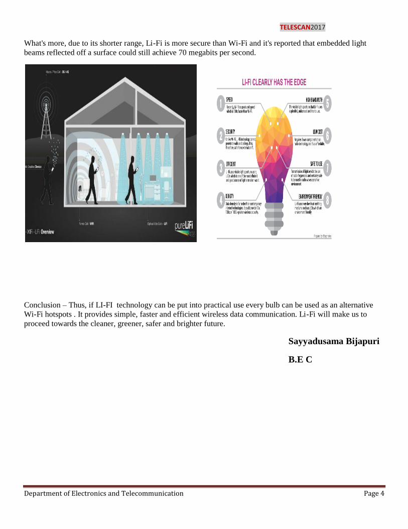
Light Fidelity (Li-Fi) is a Visible Light Communications (VLC),bidirectional, high-speed and fully
networked wireless communication technology communications travelling at very high speeds similar to Wi-Fi.
The term was coined by Harald Haas and is a form of visible light communication
Li-Fi uses common household LED (light emitting diodes) light bulbs to enable data transfer, boasting speeds
of up to 224 gigabits per second
How it works
Li-Fi and Wi-Fi are quite similar as both transmit data electromagnetically. However, Wi-Fi uses radio waves
while Li-Fi runs on visible light.
As we now know, Li-Fi is a Visible Light Communications (VLC) system. This means that it accommodates a
photo-detector to receive light signals and a signal processing element to convert the data into 'stream-able'
content.
An LED light bulb is a semi-conductor light source meaning that the constant current of electricity supplied to
an LED light bulb can be dipped and dimmed, up and down at extremely high speeds, without being visible to
the human eye.
For example, data is fed into an LED light bulb (with signal processing technology), it then sends data
(embedded in its beam) at rapid speeds to the photo-detector (photodiode).
The tiny changes in the rapid dimming of LED bulbs are then converted by the 'receiver' into electrical signal.
The signal is then converted back into a binary data stream that we would recognize as web, video and audio
applications that run on internet enables devices.
Li-Fi vs. Wi-Fi
While some may think that Li-Fi with its 224 gigabits per second leaves Wi-Fi in the dust, Li-Fi's exclusive use
of visible light could halt a mass uptake.
Li-Fi signals cannot pass through walls, so in order to enjoy full connectivity; capable LED bulbs will need to
be placed throughout the home. Not to mention, Li-Fi requires the light bulb is switched on at all times to
provide connectivity, meaning that the lights will need to be on during the day.
What's more, where there is a lack of light bulbs, there is a lack of Li-Fi internet so Li-Fi does take a hit when it
comes to public Wi-Fi networks.
.But it's not all doom and gloom! Due to its impressive speeds, Li-Fi could make a huge impact on the internet
of things too, with data transferred at much higher levels with even more devices able to connect to one another.
TELESCAN2017
Department of Electronics and Telecommunication Page 4
What's more, due to its shorter range, Li-Fi is more secure than Wi-Fi and it's reported that embedded light
beams reflected off a surface could still achieve 70 megabits per second.
Conclusion – Thus, if LI-FI technology can be put into practical use every bulb can be used as an alternative
Wi-Fi hotspots . It provides simple, faster and efficient wireless data communication. Li-Fi will make us to
proceed towards the cleaner, greener, safer and brighter future.
Sayyadusama Bijapuri
B.E C

TELESCAN2017
Department of Electronics and Telecommunication Page 5
Cloud-Computing
Cloud Computing
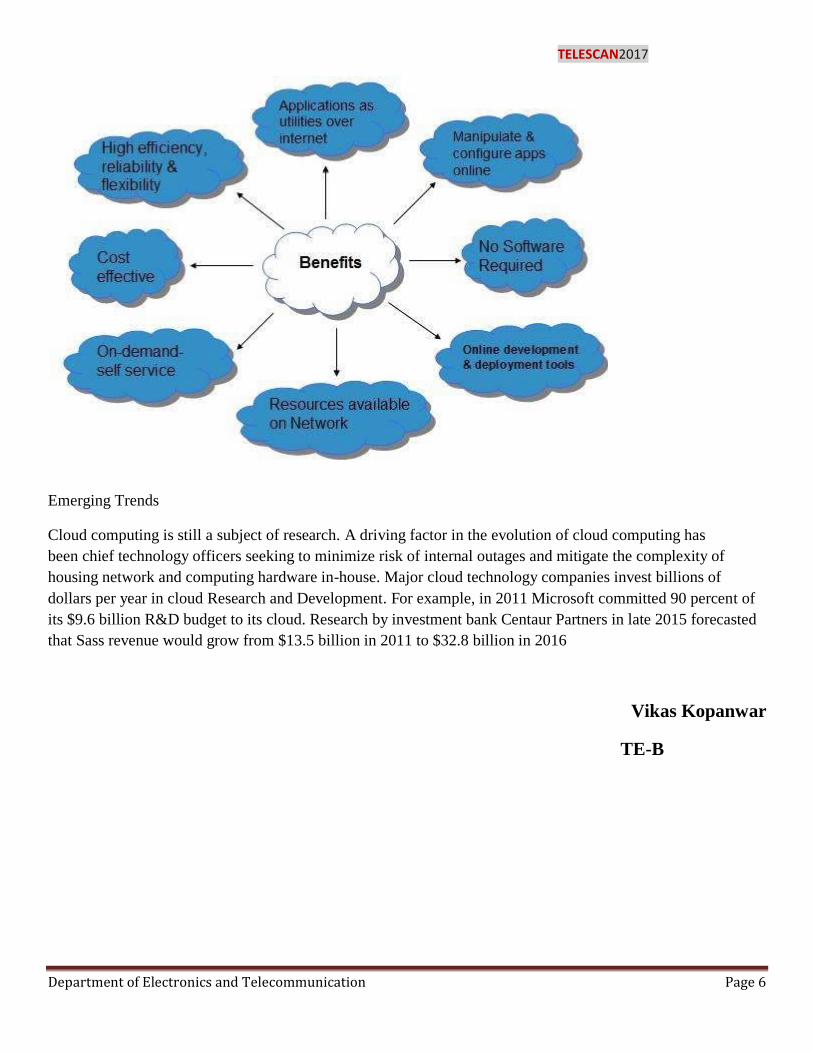
Cloud computing is a new form of Internet-based computing that provide shared computer processing resources
and data to computers and other devices on demand. It is a model for enabling ubiquitous, on-demand access to
a shared pool of configurable computing resources (e.g., computer networks, servers, storage, applications and
services), which can be rapidly provisioned and released with minimal management effort. Basically, Cloud
computing allows the users and enterprises with various capabilities to store and processes their data in either
privately owned cloud, or on a third-party server in order to make data accessing mechanisms much more easy
and reliable. Data centers that may be located far from the user–ranging in distance from across a city to across
the world. Cloud computing relies on sharing of resources to achieve coherence and economy of scale, similar
to a utility (like the electricity grid) over an electricity network.
Cloud Clients
Users access cloud computing using networked client devices, such as desktop computers, laptops, tablets and
smart phones and any Ethernet enabled device such as Home Automation Gadgets. Some of these devices—
cloud clients—rely on cloud computing for all or a majority of their applications so as to be essentially useless
without it. Examples are thin clients and the browser-based Chrome book. Many cloud applications do not
require specific software on the client and instead use a web browser to interact with the cloud application. With
Ajax and HTML5 these Web user interfaces can achieve a similar, or even better, look and feel to native
applications. Some cloud applications, however, support specific client software dedicated to these applications
(e.g., virtual desktop clients and most email clients). Some legacy applications (line of business applications
that until now have been prevalent in thin client computing) are delivered via a screen-sharing technology.
Security and privacy
Cloud computing poses privacy concerns because the service provider can access the data that is in the cloud at
any time. It could accidentally or deliberately alter or even delete information. Many cloud providers can share
information with third parties if necessary for purposes of law and order even without a warrant. That is
permitted in their privacy policies, which users must agree to before they start using cloud services. Solutions to
privacy include policy and legislation as well as end users' choices for how data is stored. Users can encrypt
data that is processed or stored within the cloud to prevent unauthorized access.
TELESCAN2017
Department of Electronics and Telecommunication Page 6
Emerging Trends
Cloud computing is still a subject of research. A driving factor in the evolution of cloud computing has
been chief technology officers seeking to minimize risk of internal outages and mitigate the complexity of
housing network and computing hardware in-house. Major cloud technology companies invest billions of
dollars per year in cloud Research and Development. For example, in 2011 Microsoft committed 90 percent of
its $9.6 billion R&D budget to its cloud. Research by investment bank Centaur Partners in late 2015 forecasted
that Sass revenue would grow from $13.5 billion in 2011 to $32.8 billion in 2016
Vikas Kopanwar
TE-B
TELESCAN2017
Department of Electronics and Telecommunication Page 7
How GPS works?
How does GPS work?
The Global Positioning System (GPS) is a network of about 30 satellites orbiting the Earth at an altitude of
20,000 km. The system was originally developed by the US government for military navigation but now anyone
with a GPS device, be it a SatNav, mobile phone or handheld GPS unit, can receive the radio signals that the
satellites broadcast.
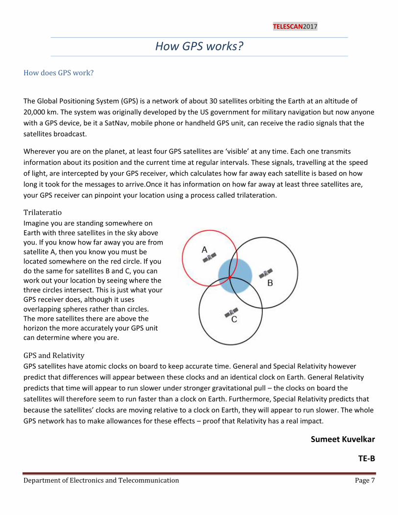
Wherever you are on the planet, at least four GPS satellites are ‘visible’ at any time. Each one transmits
information about its position and the current time at regular intervals. These signals, travelling at the speed
of light, are intercepted by your GPS receiver, which calculates how far away each satellite is based on how
long it took for the messages to arrive.Once it has information on how far away at least three satellites are,
your GPS receiver can pinpoint your location using a process called trilateration.
Trilateratio
Imagine you are standing somewhere on Earth with three satellites in the sky above you. If you know how far away you are from satellite A, then you know you must be located somewhere on the red circle. If you do the same for satellites B and C, you can work out your location by seeing where the three circles intersect. This is just what your GPS receiver does, although it uses overlapping spheres rather than circles. The more satellites there are above the horizon the more accurately your GPS unit can determine where you are.
GPS and Relativity
GPS satellites have atomic clocks on board to keep accurate time. General and Special Relativity however
predict that differences will appear between these clocks and an identical clock on Earth. General Relativity
predicts that time will appear to run slower under stronger gravitational pull – the clocks on board the
satellites will therefore seem to run faster than a clock on Earth. Furthermore, Special Relativity predicts that
because the satellites’ clocks are moving relative to a clock on Earth, they will appear to run slower. The whole
GPS network has to make allowances for these effects – proof that Relativity has a real impact.
Sumeet Kuvelkar
TE-B
TELESCAN2017
Department of Electronics and Telecommunication Page 8
More than a view- Windows double as a solar panel
A tech startup on a mission to make modern commercial and housing estates energy neutral has outfitted the
headquarters of a Dutch bank with the world's first commercial, fully transparent solar-power-generating
windows.
The windows have solar cells installed in the edges at a specific angle that allows the incoming solar light to be
efficiently transformed into electricity.
"Large commercial estates consume a lot of energy," said Ferdinand Grapperhaus, co-founder and CEO of the startup, called Physee. "If you want to make these buildings energy neutral, you never have enough roof
surface. Therefore, activating the buildings' facades will significantly contribute to making the buildings energy
neutral."The windows could generate 8 to 10 watts of power, according to Grapperhaus.
"This enables the user to charge a phone per every square meter [11 square feet] two times a day," he told Live
Science.
The first installation of Physee'sPowerWindows was unveiled in June in Eindhoven, in the south of the
Netherlands. The headquarters of Rabobank, the Netherlands' biggest bank, has been fitted with 323 square feet
(30 square m) of the Power Windows. The bank's employees will be able to plug their smart phones into the
windows using USB ports to charge their batteries, according to Physee. Other buildings in the Netherlands are
already lined up to receive the innovative solar technology, which has won Physee a place on the World
Economic Forum's Technology Pioneers 2017 list.
At the end of June, the headquarters of the Amsterdam-based charity the Postcode Lottery were fitted with the
Power Windows. After that, Physee will move forward with its first large-scale project: a 19,000-square-foot
(1,800 square m) installation in a large, newly built residential complex in Amsterdam, the bold tower.
"I believe that every new type of glass needs power," Grapperhaus said. "Either for the glass to be tinted
electrically or heated or inside windows there are these solar blinds, which are electrical and can go up and
down but also more and more you can see video glass."
Grapperhaus said that the cost of the wiring that brings power from the grid to such windows is considerable in
large commercial estates, and investing in power-generating windows would therefore make commercial sense.
Physee is already working on the next-generation technology that would triple the efficiency of the Power
Windows. The surface of the second generation of Power Windows will be coated with a special material that
transforms oncoming visible light into near-infrared light, which is then transported toward the solar cells in the
edges of the windows.
"It works similarly to a [glow-in-the-dark star]," Grapperhaus said. "The difference is that the glow star emits
the green wavelength, but the coating on our windows emits light in near-infrared wavelength."
TELESCAN2017
Department of Electronics and Telecommunication Page 9
The coating is based on the rare-earth metal thulium. Grapperhaus, together with his friend Willem Kesteloo,
discovered the ability of thulium to transform a broad spectrum of light into near-infrared light in 2014, during
their studies at the Delft University of Technology.
"Over time, our efficiency will improve further due to the development of better solar cells but also because of the economies of scale," Grapperhaus said. "Right now, we are looking for iconic projects all over the world to
show that a large glass building can be made energy neutral in an aesthetic way."
Physee was among 30 early stage technology pioneers highlighted for 2017 and selected by the World
Economic Forum for their potential to change the world. The list, announced June 14, consisted of firms
developing various technologies, including artificial intelligence, cyber security solutions and biotechnology.
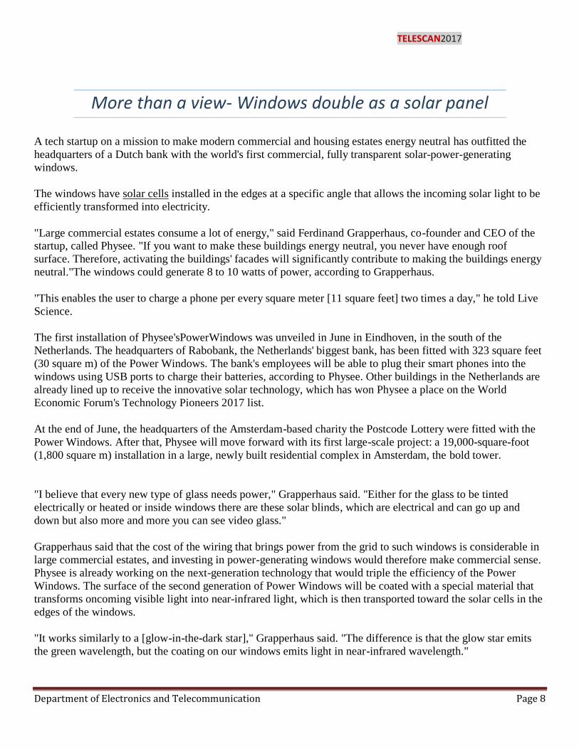
FIG: A closeup photo of one of physee’s installed Power Windows at Amsterdam’s business dstrict
Physee's presence on the list shows that the world is starting to take climate change seriously, Grapperhaus said:
"Ten years ago, sustainability was something that wasn't taken very seriously — not by venture capitalists, not
by many governments and neither by large corporations," Grapperhaus said. "What I have seen over the last
three years is that corporations are becoming more and more responsible, governments are becoming more and
more supportive, and venture capitalists are becoming more and more interested" in sustainability.
Tejaswini Muley
B.E-C

TELESCAN2017
Department of Electronics and Telecommunication Page 10
Ingestible devices that draw power from stomach acid
The device: Researchers have developed an ingestible device that uses copper and zinc electrodes to harvest
power from gastric fluid, according to a study published this week (February 6) in Nature Biomedical
Engineering. They tested the capsule in pigs, whose gastrointestinal tracts are similar to humans.
This work shows ―the feasibility of harvesting energy for several days fromGiovanni Traverso a large mammal
that is ambulating and eating,‖ said co-author of Brigham and Women‘s Hospital in Boston.
The power harvested by the device was sufficient to transmit measurements from an onboard temperature
sensor to a receiver several meters away from the animals. ―We can get relatively consistent power, enough to
power temperature measurements on a minute by minute basis and transmit [them] wirelessly,‖ explained
coauthor Phillip Nadeau of MIT.
The significance: The capsule was able to generate power from stomach acid for an average of six days—much
longer than previous devices, which were capable of harvesting energy for minutes or hours. Some earlier
ingestible electronics used a magnesium anode, but the team found that zinc anodes dissolved much less
quickly, making zinc better suited for longer-term use.
The authors demonstrated that the device could not only harvest energy in the highly acidic stomach, but also
harvested small amounts of energy in the small intestine, where the pH is closer to neutral. They used a version
of the device to measure the power available in both the stomach and the small intestine, which should help
researchers improve future ingestible electronics.
Jiang added that the design of the capsule, where the zinc anode and copper cathode freely contact gastric fluid,
is also advantageous because there is no danger of leakage. ―Usually if you have a battery inside the body, you
have to package the battery with certain materials that are inert and seal the electrodes and the electrolyte
inside,‖ he explained. In that case, ―you could potentially have leakage [of the] electrolyte into the human fluid,
which is harmful or toxic.‖
Needs improvement: The researchers built the device from commercially available parts, which resulted in a
relatively large capsule, about the size of a triple A battery.
―I don‘t think anyone would want to swallow‖ a 3.5 centimeter long, 1.2 cm in diameter capsule, said Nadeau.
―It‘s a mega pill, so the first step is obviously miniaturization.‖
―A general question for anyone designing this class of devices [is] the tension between miniaturization and
utility,‖ said Christopher Bettinger of Carnegie Mellon University in Pittsburgh, Pennsylvania, who was not
involved in the work.
In the current study, the authors showed that the device could trigger drug delivery with harvested energy in an
in vitro system. Bettinger said that using small devices for drug delivery could present challenges based on the
amount of drug that can be loaded. And ―microelectronic devices can get smaller and smaller, but there are
thermodynamic limits to how small you can make a battery,‖ he noted.
TELESCAN2017
Department of Electronics and Telecommunication Page 11
The future: Nadeau said that building smaller capsules is achievable in the short term, and that the current
measurements of potential energy in different segments of the gastrointestinal tract will inform the team‘s
design.
Another goal of future work is adding different types of sensors, perhaps for pH and pressure. Capsules with
more sophisticated sensing abilities could have health implications.
―Stomach ulcers can become cancerous,‖ said Sameer Sonkusale of Tufts University in Medford,
Massachusetts, who did not participate in the work, ―so if you put sensors in that can actually monitor how your
gut lining is doing, then you might be able to prevent ulcers from becoming tumors and take preventive action.‖
Aditya Saraiya
S.E C
TELESCAN2017
Department of Electronics and Telecommunication Page 12
New thermal abilities for semiconductor
What would a simple technique to remove thin layers from otherwise thick, rigid semiconductor crystals mean
for the semiconductor industry? This concept has been actively explored for years, as integrated circuits made
on thin layers hold promise for developments including improved thermal characteristics, lightweight
stackability and a high degree of flexibility compared to conventionally thick substrates.
In a significant advance, a research group from IBM successfully applied their new "controlled spalling" layer
transfer technique to gallium nitride (GaN) crystals, a prevalent semiconductor material, and created a pathway
for producing many layers from a single substrate.
Their method boils down to simply peeling off the tape, nickel layer and a thin layer of the substrate material
stuck to the nickel.
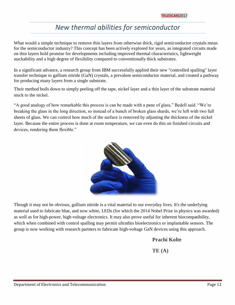
―A good analogy of how remarkable this process is can be made with a pane of glass,‖ Bedell said. ―We‘re
breaking the glass in the long direction, so instead of a bunch of broken glass shards, we‘re left with two full
sheets of glass. We can control how much of the surface is removed by adjusting the thickness of the nickel
layer. Because the entire process is done at room temperature, we can even do this on finished circuits and
devices, rendering them flexible.‖
Though it may not be obvious, gallium nitride is a vital material to our everyday lives. It's the underlying
material used to fabricate blue, and now white, LEDs (for which the 2014 Nobel Prize in physics was awarded)
as well as for high-power, high-voltage electronics. It may also prove useful for inherent biocompatibility,
which when combined with control spalling may permit ultrathin bioelectronics or implantable sensors. The
group is now working with research partners to fabricate high-voltage GaN devices using this approach.
Prachi Kolte
TE (A)
TELESCAN2017
Department of Electronics and Telecommunication Page 13
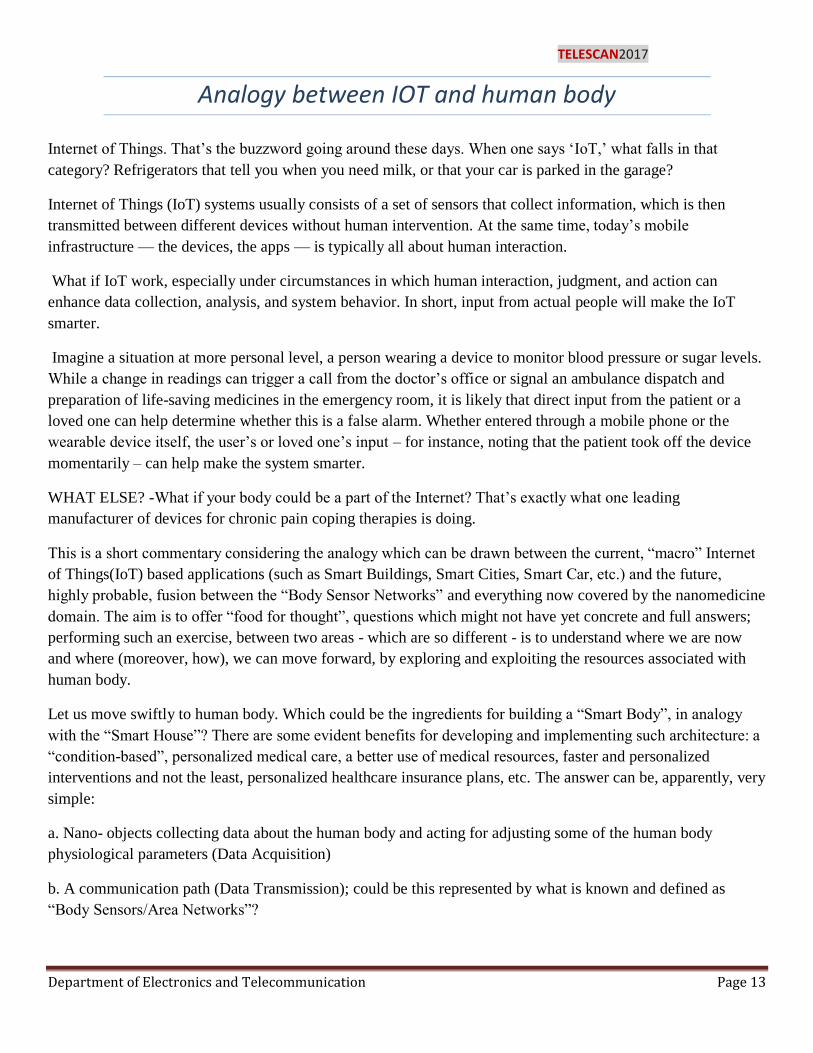
Analogy between IOT and human body
Internet of Things. That‘s the buzzword going around these days. When one says ‗IoT,‘ what falls in that
category? Refrigerators that tell you when you need milk, or that your car is parked in the garage?
Internet of Things (IoT) systems usually consists of a set of sensors that collect information, which is then
transmitted between different devices without human intervention. At the same time, today‘s mobile
infrastructure — the devices, the apps — is typically all about human interaction.
What if IoT work, especially under circumstances in which human interaction, judgment, and action can
enhance data collection, analysis, and system behavior. In short, input from actual people will make the IoT
smarter.
Imagine a situation at more personal level, a person wearing a device to monitor blood pressure or sugar levels.
While a change in readings can trigger a call from the doctor‘s office or signal an ambulance dispatch and
preparation of life-saving medicines in the emergency room, it is likely that direct input from the patient or a
loved one can help determine whether this is a false alarm. Whether entered through a mobile phone or the
wearable device itself, the user‘s or loved one‘s input – for instance, noting that the patient took off the device
momentarily – can help make the system smarter.
WHAT ELSE? -What if your body could be a part of the Internet? That‘s exactly what one leading
manufacturer of devices for chronic pain coping therapies is doing.
This is a short commentary considering the analogy which can be drawn between the current, ―macro‖ Internet
of Things(IoT) based applications (such as Smart Buildings, Smart Cities, Smart Car, etc. and the future,
highly probable, fusion between the ―Body Sensor Networks‖ and everything now covered by the nanomedicine
domain. The aim is to offer ―food for thought‖, questions which might not have yet concrete and full answers;
performing such an exercise, between two areas - which are so different - is to understand where we are now
and where (moreover, how), we can move forward, by exploring and exploiting the resources associated with
human body.
Let us move swiftly to human body. Which could be the ingredients for building a ―Smart Body‖, in analogy
with the ―Smart House‖? There are some evident benefits for developing and implementing such architecture: a
―condition-based‖, personalized medical care, a better use of medical resources, faster and personalized
interventions and not the least, personalized healthcare insurance plans, etc. The answer can be, apparently, very
simple:
a. Nano- objects collecting data about the human body and acting for adjusting some of the human body
physiological parameters (Data Acquisition)
b. A communication path (Data Transmission); could be this represented by what is known and defined as
―Body Sensors/Area Networks‖?
TELESCAN2017
Department of Electronics and Telecommunication Page 14
c. A Local Data Processing unit and further on, a connection to the CLOUD (for further Data Processing and
Decision Taking).It will tight the nanomedicine to the wider domain of medicine.
The devices in question provide chronic pain coping therapy by sending small, highly-tailored electrical pulses
directly into the spinal column. These are used in addition to, or preferably instead of, traditional opioid or other
pain relief medications. The intention of these devices and therapies is to reduce or eliminate dependency on
medications and increase the patient's quality of life. These devices are implanted inside the patient‘s body and
electrodes are placed inside the spinal column to provide the therapy.
But every person has a different type of pain; therefore the placement of electrodes varies. After the device is
implanted, the patient will resume their daily life and manage their pain as needed using the device and a radio
frequency based remote control. During their daily routines and movements, the placement of the electrodes in
the patient‘s spinal column can shift.
IoT systems are continuing to roll out across industries, such as health management, industrial production,
logistics, and retail, among many others. The key to maximizing the usefulness IoT systems is getting these
mobile interactions right. We should look for opportunities to improve the capabilities of IoT environments by
making it easier for real people to contribute to them.
Meenu Krishna
SE
TELESCAN2017
Department of Electronics and Telecommunication Page 15
Breathable, wearable electronics on skin for long-term
health monitoring
A hypoallergenic electronic sensor can be worn on the skin continuously for a week without discomfort, and is
so light and thin that users forget they even have it on, says a Japanese group of scientists. The elastic electrode
constructed of breathable nanoscale meshes holds promise for the development of noninvasive e-skin devices
that can monitor a person's health continuously over a long period. Wearable electronics that monitor heart rate
and other vital health signals have made headway in recent years, with next-generation gadgets employing
lightweight, highly elastic materials attached directly onto the skin for more sensitive, precise measurements.
However, although the ultrathin films and rubber sheets used in these devices adhere and conform well to the
skin, their lack of breathability is deemed unsafe for long-term use: dermatological tests show the fine,
stretchable materials prevent sweating and block airflow around the skin, causing irritation and inflammation,
which ultimately could lead to lasting physiological and psychological effects.
"We learned that devices that can be worn for a week or longer for continuous monitoring were needed for
practical use in medical and sports applications," says Professor Takao Someya at the University of Tokyo's
Graduate School of Engineering whose research group had previously developed an on-skin patch that
measured oxygen in blood.
In the current research, the group developed an electrode constructed from nanoscale meshes containing a
water-soluble polymer, polyvinyl alcohol (PVA), and a gold layer -- materials considered safe and biologically
compatible with the body. The device can be applied by spraying a tiny amount of water, which dissolves the
PVA nanofibers and allows it to stick easily to the skin -- it conformed seamlessly to curvilinear surfaces of
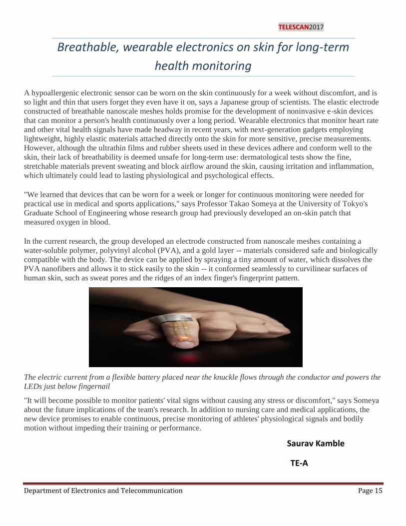
human skin, such as sweat pores and the ridges of an index finger's fingerprint pattern.
The electric current from a flexible battery placed near the knuckle flows through the conductor and powers the
LEDs just below fingernail
"It will become possible to monitor patients' vital signs without causing any stress or discomfort," says Someya
about the future implications of the team's research. In addition to nursing care and medical applications, the
new device promises to enable continuous, precise monitoring of athletes' physiological signals and bodily
motion without impeding their training or performance.
Saurav Kamble
TE-A
TELESCAN2017
Department of Electronics and Telecommunication Page 16
2-D Electronics
For about a decade, 2D (two-dimensional) materials have represented one of the latest directions in solid-state
research. The rise of 2D materials began in 2004, when the Novoselov–Geim group from the University of
Manchester and the group of Berger and de Heer from Georgia Tech published their pioneering papers on
graphene, a 2D material consisting of a single layer of carbon atoms arranged in a honeycomb lattice. Since
graphene shows outstanding properties, e.g., very high carrier mobilities, excellent heat conductivity, and
superior mechanical strength, researchers from various communities including physicists, chemists, material
scientists, electronics engineers, etc., became fascinated by this new material. An impression on the unabatedly
strong interest in graphene can be obtained by counting the papers listed in the database Web of Science under
the search term ―graphene‖. For 2004, one finds 183 entries compared to over 7000 for 2010 and more than
34,300 for the year 2015, which exceeds the number for 2014 by more than 5000.
Interest in the field started with the discovery of graphene, a structural variant of carbon. Carbon atoms in
graphene form a hexagonal two-dimensional lattice, and this atom-thick layer has attracted attention due to its
high electrical and thermal conductivity, mechanical flexibility and very high tensile strength. Graphene is the
strongest material ever tested. In 2010, the Royal Swedish Academy of Sciences decided to award the Nobel
Prize in Physics to Andre Geim and Konstantin Novoselov for their ―groundbreaking experiments‖ in
grapheneresearch. Graphene may have started this 2D revolution in electronics, but silicene, phosphorene and
stanene, atom-thick allotropes of silicon, phosphorus and tin, respectively, have a similar honeycomb structure
with different properties, resulting in different applications. All four have the potential to change electronics as
we know it, allowing for miniaturization, higher performance and cost reduction. Several companies around the
globe, including Samsung and Apple, are developing applications based on graphene.
A two-dimensional semiconductor (also known as 2D semiconductor) is a type of natural semiconductor with
thicknesses on the atomic scale. The rising research attention towards 2D semiconductors started with a
discovery by Geim and Novoselov et al. in 2004, when they reported a new semiconducting material graphene,
a flat monolayer of carbon atoms arranged in a 2D honeycomb lattice. A 2D monolayer semiconductor is
significant because it exhibits stronger piezoelectric coupling than traditionally employed bulk forms, which
enables 2D materials applications in new electronic components used for sensing and actuating. In this
emergent field of research in solid-state physics, the main focus is currently on designing Nano
electronic components by the use of graphene as electrical conductor, hexagonal boron nitride as electrical
insulator, and a transition metal dichalcogenide as semiconductor.
Graphene has attracted considerable research interest over the last few years because it exhibits unique
mechanical behaviors with the capability to support a range of important flexible electronic applications, which
would be difficult to achieve using materials that exist today. In recent years, many research groups have
explored the fundamental physics associated with the properties of graphene for flexible electronics, the
fabrication methods that allow its assembly into integrated structures on unusual substrates such as plastic and
rubber, and various examples of unique applications enabled by graphene. This focus issue includes the entire

TELESCAN2017
Department of Electronics and Telecommunication Page 17
range of fundamental, applied and practical subjects associated with the development of graphene-based
flexible devices, with wide-ranging relevance in electronics, photonics, photovoltaic and advanced sensors.
Figure 1. Schematic illustrating advantages of 2D materials: surfaces of (a) 3D and (b) 2D materials. The
pristine interfaces (without out-of-plane dangling bonds) of 2D materials help reduce the interface traps. Mobile
charge distribution in (c) 3D and (d) 2D crystals is used as channel materials. The carrier confinement effect in
2D materials leads to excellent gate electrostatics. (e) Various types of 2D materials from insulator to
superconductor. E.g. denotes the band gap.
Mansi Dadir
BE-C

TELESCAN2017
Department of Electronics and Telecommunication Page 18
Organic Electronics
The development of conducting polymers and their applications resulted in another Nobel prize in 2000, this
time in chemistry. Alan J. Heeger, Alan G. MacDiarmid and Hideki Shirakawa proved that plastic can conduct
electricity.
Unlike conventional inorganic conductors and semiconductors, organic electronic materials are constructed
from organic (carbon-based) molecules or polymers using chemical synthesis. Organic electronics is not limited
to conducting polymers, but includes other organic materials that might be of use in electronics. These include a
variety of dyes, organic charge-transfer complexes, and many other organic molecules.
In terms of performance and industrial development, organic molecules and polymers cannot yet compete with
their inorganic counterparts. However, organic electronics have some advantages over conventional electronic
materials. Low material and production costs, mechanical flexibility, adaptability of synthesis processes and
biocompatibility make organic electronics a desirable choice for certain applications.
History
One class of materials of interest in organic electronics are electrical conductive, i.e. substances that can
transmit electrical charges with low resistivity. Traditionally, conductive materials are inorganic. Classical (and
still technologically dominant) conductive materials are metals such as copper and aluminum as well as
many alloys.
The earliest reported organic conductive material, polyaniline, was described by Henry Letheby in 1862. Work
on other polymeric organic materials began in earnest in the 1960s, A high conductivity of 1 S/cm (S
= Siemens) was reported in 1963 for a derivative of tetraiodopyrrole.[4]
In 1977, it was discovered
that polyacetylene can be oxidized with halogens to produce conducting materials from
either insulating or semiconducting materials.
Conductive polymers are lighter, more flexible, and less expensive than inorganic conductors. This makes them
a desirable alternative in many applications. It also creates the possibility of new applications that would be
impossible using copper or silicon.
Organic electronics not only includes organic semiconductors, but also organic dielectrics, conductors and light
emitters.

TELESCAN2017
Department of Electronics and Telecommunication Page 19
New applications include smart windows and electronic paper. Conductive polymers are expected to play an
important role in the emerging science of molecular computers.
OFET classification and current research
Rubrene-OFET with highest charge mobility
Like OLEDs, OFETs can be classified into small-molecule and polymer-based system. Charge transport in
OFETs can be quantified using a measure called carrier mobility; currently, rubrene-based OFETs show the
highest carrier mobility of 20–40 cm2/ (V·s). Another popular OFET material is Pentacene. Due to its

TELESCAN2017
Department of Electronics and Telecommunication Page 20
low solubility in most organic solvents, it's difficult to fabricate thin film transistors (TFTs) from pentacene
itself using conventional spin-cast or, dip coating methods, but this obstacle can be overcome by using the
derivative TIPS-pentacene. Current research focuses more on thin-film transistor (TFT) model, which
eliminates the usage of conductive materials. Very recently, two studies conducted by Dr. Bao Z.[16]
et al. and
Dr. Kim J. et al. demonstrated control over the formation of designed thin-film transistors. By controlling the
formation of crystalline TFT, it is possible to create an aligned (as opposed to randomly ordered) charge
transport pathway, resulting in enhanced charge mobility.
Commercially available high-tech products relying on organic semiconductors, such as curved television
screens, displays for smart phones, colored light sources and portable solar cells, demonstrate the industrial
maturity of organic electronics. In fact, several high-tech companies, including LG Electronics and Samsung,
have invested in cheap and high-performance organic-electronic devices. It is expected that the organic
electronics market will grow rapidly in the coming years.
Prachi Kolte
TE-A
TELESCAN2017
Department of Electronics and Telecommunication Page 21
Memristor
What is a memristor? Memristors are basically a fourth class of electrical circuit, joining the resistor, the
capacitor, and the inductor, that exhibit their unique properties primarily at the nanoscale. Theoretically,
Memristors, a concatenation of ―memory resistors‖, are a type of passive circuit elements that maintain a
relationship between the time integrals of current and voltage across a two terminal element. Thus, a memristors
resistance varies according to a devices memristance function, allowing, via tiny read charges, access to a
―history‖ of applied voltage. The material implementation of memristive effects can be determined in part by
the presence of hysteresis (an accelerating rate of change as an object moves from one state to another) which,
like many other non-linear ―anomalies‖ in contemporary circuit theory, turns out to be less an anomaly thana
fundamental property of passive circuitry.
Until recently, when HP Labs under Stanley Williams developed the first stable prototype, memristance as a
property of a known material was nearly nonexistent. The memristance effect at non-nanoscale distances is
dwarfed by other electronic and field effects, until scales and materials that are nanometers in size are utilized.
At the nanoscale, such properties have even been observed in action prior to the HP Lab prototypes.
But beyond the physics of electrical engineering, they are a reconceptualizing of passive electronic circuit
theory first proposed in 1971 by the nonlinear circuit theorist Leon Chua. What Leon Chua, a UC Berkeley
Professor, contended in his 1971 paper Transactions on Circuit Theory, is that the fundamental relationship in
passive circuitry was not between voltage and charge as assumed, but between changes-in-voltage, or flux, and
charge. Chua has stated: ―The situation is analogous to what is called ―Aristotle‘s Law of Motion, which was
wrong, because he said that force must be proportional to velocity. That misled people for 2000 years until
Newton came along and pointed out that Aristotle was using the wrong variables. Newton said that force is
proportional to acceleration–the change in velocity. This is exactly the situation with electronic circuit theory
today. All electronic textbooks have been teaching using the wrong variables–voltage and charge–explaining
away inaccuracies as anomalies. What they should have been teaching is the relationship between changes in
voltage, or flux, and charge.‖
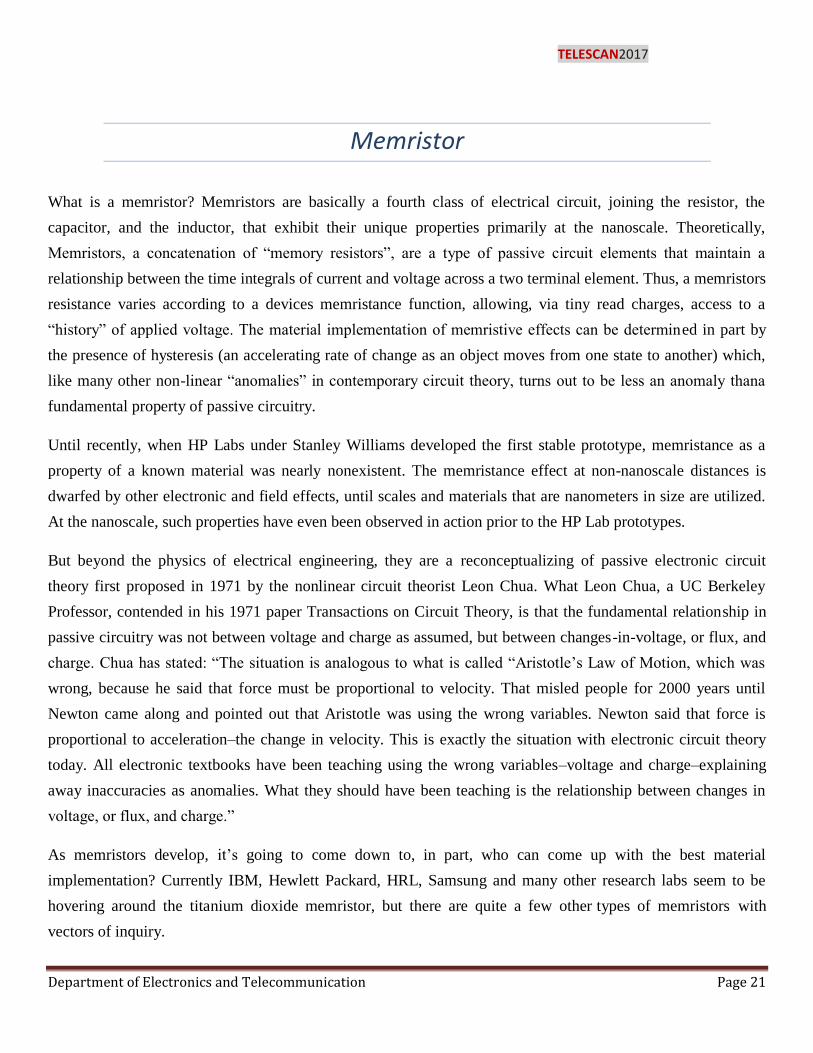
As memristors develop, it‘s going to come down to, in part, who can come up with the best material
implementation? Currently IBM, Hewlett Packard, HRL, Samsung and many other research labs seem to be
hovering around the titanium dioxide memristor, but there are quite a few other types of memristors with
vectors of inquiry.

TELESCAN2017
Department of Electronics and Telecommunication Page 22
Conceptual symmetries of resistor, capacitor, inductor, and memristor.
Memristor Construction
A physical memristor comprises a two-terminal device whose resistance depends on the polarity, magnitude,
and also span of time of the voltage applied to it. When the voltage is switched off, then the resistance leftovers
as it did just already it was turned off. This makes this device as a nonlinear, nonvolatile memory device.
Memristor Construction.
The above showed two terminal memristor uses TiO2 (titanium dioxide) as the resistive material. Here TiO2
works better than the other materials like SiO2.Once a voltage is applied across the platinum electrodes, oxygen
atoms in the material diffuse right or left, depending on the voltage polarity, which makes the solid thinner or
thicker, thus producing a change in resistance.
Different Types of Memristors
There are quite a few vectors of review researching various types of memristors. The material execution of a
memristor is significant to how they act in a memristive system. It‘s essential to recognize the difference
TELESCAN2017
Department of Electronics and Telecommunication Page 23
between a memristor& a memristive system because the exact type of memristor can focus different assets and
faults, and they can be used in a memristive system for different applications to measure or purpose. There are
currently no memristor data sheets available for memristor, as much of the material executions are trying and in
progress.
Classification of Memristor
Benefits of Memristor
The benefits of memristor technology include the following
Memristors do not consume power when idle and are comfortable with CMOS interfaces.
Would allow for a faster boot up since information is not lost when the device is turned off.
Would allow for a faster boot up since information is not lost when the device is turned off.
Memristor= Hard disk + RAM
It uses less energy and generates less heat.
It uses less energy and generates less heat.
It removes the need to write computer programs that repeat small parts of the brain.
As a non-volatile memory, memristors do not consume power when idle.
Creating an analog computer that works much faster than digital ones.
It offers greater resiliency and reliability when power is interrupted in data centers.
Density lets for more information to be stored.
Nikhil Bangad
TE-C

TELESCAN2017
Department of Electronics and Telecommunication Page 24
Color-shifting electronic skin could have wearable tech and
prosthetic uses
Researchers have developed a new type of user-interactive electronic skin, with a color change perceptible to
the human eye, and achieved with a much-reduced level of strain. Their results could have applications in
robotics, prosthetics and wearable technology. The ability of some animals, including chameleons, octopus, and
squid, to change their skin colour for camouflage, temperature control, or communication is well known.
While science has been able to replicate these abilities with artificial skin, the colour changes are often only
visible to the naked eye when the material is put under huge mechanical strain.
Now, however, researchers in China have developed a new type of user-interactive electronic skin, with a color
change perceptible to the human eye, and achieved with a much-reduced level of strain. Their results could have
applications in robotics, prosthetics and wearable technology.
The Tsinghua University in Beijing, employed flexible electronics made from graphene, in the form of a highly-
sensitive resistive strain sensor, combined with a stretchable organic electrochromic device.
DrTingting Yang, from Tsinghua University, said: "We explored the substrate (underlying) effect on the
electromechanical behavior of graphene. To obtain good performance with a simple process and reduced cost,
we designed a modulus-gradient structure to use graphene as both the highly sensitive strain-sensing element
and the insensitive stretchable electrode of the ECD layer.
"We found subtle strain -- between zero and 10 per cent -- was enough to cause an obvious colour change, and
the RGB value of the colour quantified the magnitude of the applied strain."
Professor Hongwei Zhu said: "Graphene, with its high transparency, rapid carrier transport, flexibility and large
specific surface area, shows application potential for flexible electronics, including stretchable electrodes,
supercapacitor, sensors, and optical devices.

TELESCAN2017
Department of Electronics and Telecommunication Page 25
"However, our results also show that the mechanical property of the substrate was strongly relevant to the
performance of the strain sensing materials. This is something that has previously been somewhat overlooked,
but that we believe should be closely considered in future studies of the electromechanical behavior of certain
functional materials."
Dr Yang said: "It's important to note that the capability we found for interactive color changes with such a small
strain range has been rarely reported before. This user-interactive e-skin should be promising for applications in
wearable devices, robots and prosthetics in the future."
Saurav Kamble
TE-A
TELESCAN2017
Department of Electronics and Telecommunication Page 26
Spintronics
Electronics is based on measuring the tiny electrical charge of electrons passing through electronic circuits. An
alternative approach under development is spintronics, which instead relies not on electrons' charge, but on
another of their fundamental quantum-mechanical properties: spin.
Spin can be visualized as the Earth turning on its own axis while rotating around the sun. In the same way, an
electron spins on its own axis while rotating around an atom's nucleus. Spin is either "up" or "down". In the
same way traditional electronics uses charge to represent information as zeros and ones, the two spin states can
be used to represent the same binary data in spintronics.
Spin can be measured because it generates tiny magnetic fields. Ferrous metals such as iron become magnetic,
for example, when enough particles have their spin set in the same direction, generating a magnetic field of the
same polarity as the spin.
Spintronics has several advantages over conventional electronics. Electronics require specialized semiconductor
materials in order to control the flow of charge through the transistors. But spin can be measured very simply in
common metals such as copper or aluminum. Less energy is needed to change spin than to generate a current to
maintain electron charges in a device, so spintronics devices use less power.
Spin states can be set quickly, which makes transferring data quicker. And because electron spin is not energy-
dependent, spin is non-volatile – information sent using spin remains fixed even after loss of power.
Why spin?
We begin with the question, "What is special about electron spin?" From a scientific and technological point of
view, there are four important points. First is the connection between spin and magnetism, which is useful for
information storage. Second is an intrinsic connection between spin and quantum mechanics, which may be
useful for quantum information. Third is the short range of spin-dependent exchange interactions, which implies
that the role of spin will continue to grow as the size of nanostructures continues to shrink. Fourth are the issues
of speed and power dissipation, which are becoming increasingly important for electronics at the nanoscale.
First, spin is connected to ferromagnetic materials because the spontaneous magnetization breaks time-reversal
symmetry, which allows the electronic states within the material to become spin-dependent. This contrasts with
non-magnetic materials where time-reversal symmetry forces the electronic states to come in pairs with the
same energy but opposite spin, thus leading to a density of states that must be independent of spin. In the
ferromagnetic metal, the density of states (DOS) is different for the two spin states. It is conventional to refer to
the majority spin as "spin up" while the minority spin is "spin down." Because most transport properties depend
on the density of states near the Fermi level, the spin asymmetry in the density of states allows ferromagnets to
generate, manipulate, and detect spin.
TELESCAN2017
Department of Electronics and Telecommunication Page 27
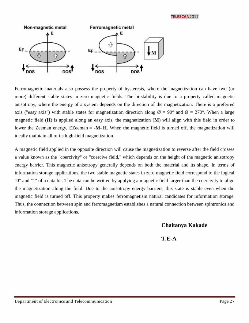
Ferromagnetic materials also possess the property of hysteresis, where the magnetization can have two (or
more) different stable states in zero magnetic fields. The bi-stability is due to a property called magnetic
anisotropy, where the energy of a system depends on the direction of the magnetization. There is a preferred
axis ("easy axis") with stable states for magnetization direction along Ø = 90° and Ø = 270°. When a large
magnetic field (H) is applied along an easy axis, the magnetization (M) will align with this field in order to
lower the Zeeman energy, EZeeman = -M- H. When the magnetic field is turned off, the magnetization will
ideally maintain all of its high-field magnetization.
A magnetic field applied in the opposite direction will cause the magnetization to reverse after the field crosses
a value known as the "coercivity" or "coercive field," which depends on the height of the magnetic anisotropy
energy barrier. This magnetic anisotropy generally depends on both the material and its shape. In terms of
information storage applications, the two stable magnetic states in zero magnetic field correspond to the logical
"0" and "1" of a data bit. The data can be written by applying a magnetic field larger than the coercivity to align
the magnetization along the field. Due to the anisotropy energy barriers, this state is stable even when the
magnetic field is turned off. This property makes ferromagnetism natural candidates for information storage.
Thus, the connection between spin and ferromagnetism establishes a natural connection between spintronics and
information storage applications.
Chaitanya Kakade
T.E-A
TELESCAN2017
Department of Electronics and Telecommunication Page 28
Sticky insect sized drones to pollinate crops
Japanese scientists have developed tiny insect-sized drones coated with horse hair and a sticky gel that may help
pollinate crops in future and offset the costly decline of bee populations worldwide.
The undersides of these artificial pollinators are coated with horse hairs and an ionic gel just sticky enough to
pick up pollen from one flower and deposit it onto another.
The researchers are hopeful that their invention could someday help carry the burden that modern agricultural
demand has put on colonies and in turn benefit farmers.
"The findings, which will have applications for agriculture and robotics, could lead to the development of
artificial pollinators and help counter the problems caused by declining honeybee populations," said
EijiroMiyako, a chemist at the National Institute of Advanced Industrial Science and Technology (AIST)
Nanomaterial Research Institute in Japan.
"We believe that robotic pollinators could be trained to learn pollination paths using global positioning systems
and artificial intelligence," said Miyako
In 2007, Miyako was working to make liquids that could be used as electrical conductors. One of his attempts
generated a gel as sticky as hair wax, which he considered a failure.
Inspired by concerns over honeybees and news reports on robotic insects, Miyako began to explore, by using
houseflies and ants, whether the gel could work to pick up pollen.
"This project is the result of serendipity," said Miyako, who worked with postdoctoral fellow Svetlana
Chechetka.
To determine whether the gel could grasp onto pollen, Miyako collected ants, put the ionic goop droplet on their
bodies, and left them to roam free in a box of tulips.
Compared with ants that did not have the material applied, the ants with the gel were more likely to have pollen
attached to their bodies.
In separate experiments using houseflies, the gel was also found to have a camouflage effect - changing colour
in response to different sources of light - which could help artificial pollinators avoid predation.
Miyako next needed a flying machine that was small enough to manoeuvre across a field of flowers, like a bee.
He settled on a four-propeller drone, costing USD 100, but simply placing the gel on its smooth, plastic surface
would not be enough for it to effectively pick up pollen.
Researchers used horse hair to mimic the fuzzy exterior of a bee. The bristles create more surface area for
pollen to adhere to and generate electric charge to keep the grains in place.
Miyako‘s team flew the remote-controlled drones, with hairs and gel attached, over the flowers of pink-leaved
Japanese lilies (Liliumjaponicum).

TELESCAN2017
Department of Electronics and Telecommunication Page 29
The robots absorbed the pollen and then could be flown to a second flower, where the grains were deposited,
artificially pollinating the plants and causing them to begin the process of producing seeds. Drones without the
gel and hair components did not have this effect.
Prachi Kolte
TE-A