Embed Size (px)
Citation preview
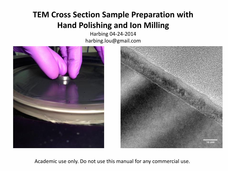
TEM Cross Section Sample Preparation with Hand Polishing and Ion Milling
Harbing 04-24-2014 [email protected]
Academic use only. Do not use this manual for any commercial use.
Sample requirement: A relatively smooth surface on a solid wafer substrate is very desirable for hand polishing TEM cross section sample prep. In order to see a very clear interface between the film and the substrate, a thinner film would be better. Generally, film thicker than 200nm would be very difficult for a interface imaging. Usually the film should be somewhat stable in air and water since the polishing step is performed in water. However, the final ion milling step would be performed in vacuum chamber and the water exposed part will be sputtered away. A single crystal substrate would be very desirable for TEM imaging work. But very hard substrates ( like sapphire and diamond) would be very challenging for the polishing and ion milling steps.
Instruments and materials needed Instruments: Polisher, Gatan precision mill, diamond stylus, “crystal stub” and “metal ring” Materials: Ted Pella SiC sand paper (600, 800, 1200), colloidal silica or alumina (0.02~0.05um) Epoxy: Two part epoxy, crystal bond, 5min epoxy. TEM grid: Ted Pella Pelco Synap grids would work pretty good. Glass slides and dicing cutter.
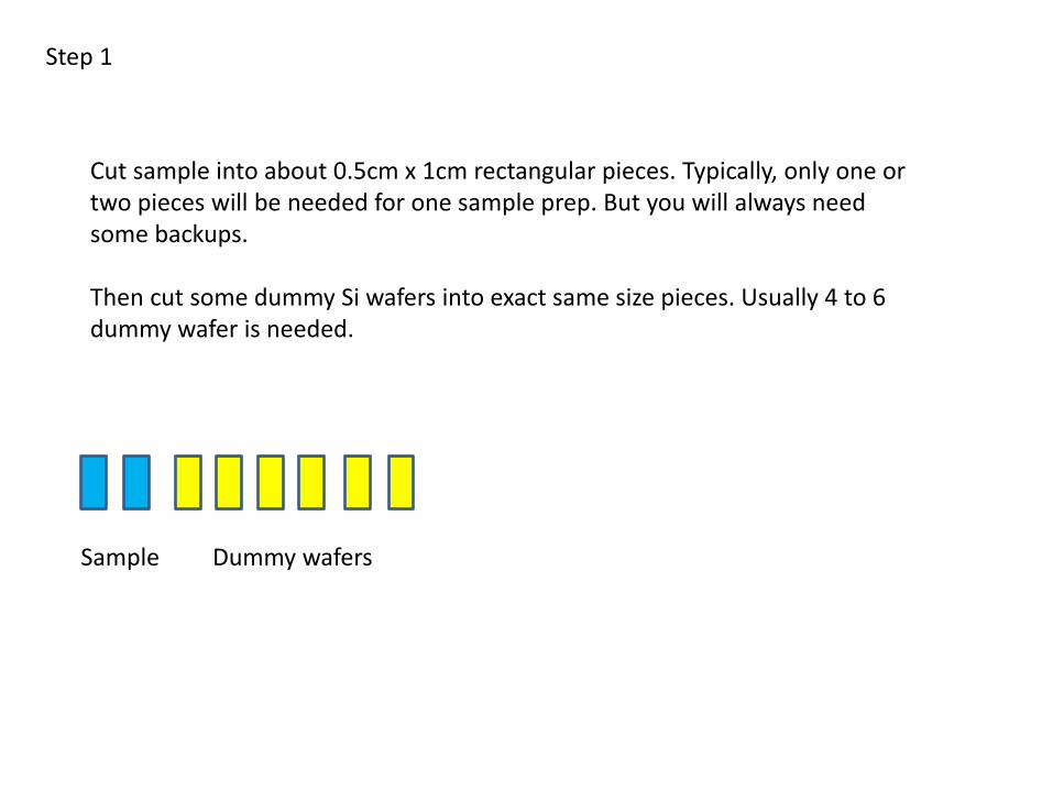
Step 1
Cut sample into about 0.5cm x 1cm rectangular pieces. Typically, only one or two pieces will be needed for one sample prep. But you will always need some backups. Then cut some dummy Si wafers into exact same size pieces. Usually 4 to 6 dummy wafer is needed.
Dummy wafers Sample
Step 2
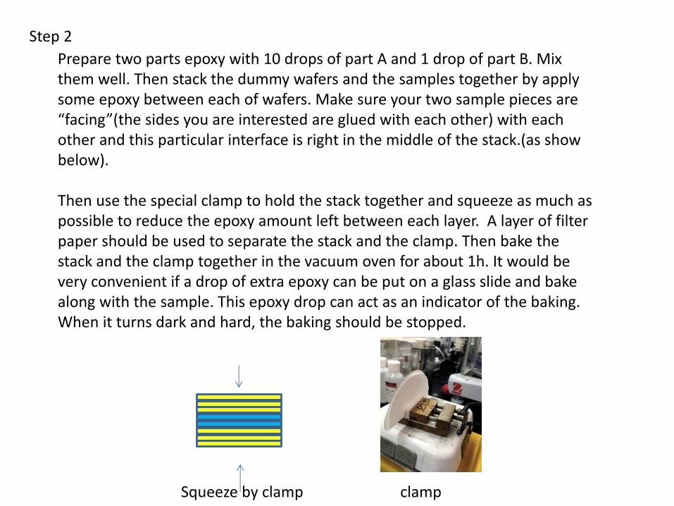
Prepare two parts epoxy with 10 drops of part A and 1 drop of part B. Mix them well. Then stack the dummy wafers and the samples together by apply some epoxy between each of wafers. Make sure your two sample pieces are “facing”(the sides you are interested are glued with each other) with each other and this particular interface is right in the middle of the stack.(as show below). Then use the special clamp to hold the stack together and squeeze as much as possible to reduce the epoxy amount left between each layer. A layer of filter paper should be used to separate the stack and the clamp. Then bake the stack and the clamp together in the vacuum oven for about 1h. It would be very convenient if a drop of extra epoxy can be put on a glass slide and bake along with the sample. This epoxy drop can act as an indicator of the baking. When it turns dark and hard, the baking should be stopped.
clamp Squeeze by clamp

Step 3
After the baking, heat up a glass slide on the hot place and melt a little bit crystal bond on it. Then attach the stack on to the slide. Make sure the long edge of the stack is parallel with the long edge of the slide(in some special cases you might need to tilt the stack deliberately) as shown below. Then mount the slide on to the dicing cutter in the way that has shown in the photo below. Make sure that the dicing saw is cutting on the stack evenly. Once the stack has been cutted through, lift the lever up and shift the whole lever by turning the nob on the right side for around 1.5mm. Then cut the stack again. In this way. A 1mm thick slice could be obtained.
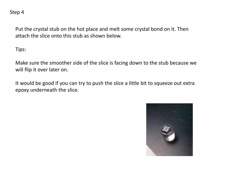
Step 4
Put the crystal stub on the hot place and melt some crystal bond on it. Then attach the slice onto this stub as shown below. Tips: Make sure the smoother side of the slice is facing down to the stub because we will flip it over later on. It would be good if you can try to push the slice a little bit to squeeze out extra epoxy underneath the slice.
Step 5 Polish first side
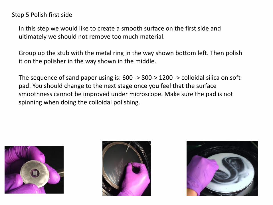
In this step we would like to create a smooth surface on the first side and ultimately we should not remove too much material. Group up the stub with the metal ring in the way shown bottom left. Then polish it on the polisher in the way shown in the middle. The sequence of sand paper using is: 600 -> 800-> 1200 -> colloidal silica on soft pad. You should change to the next stage once you feel that the surface smoothness cannot be improved under microscope. Make sure the pad is not spinning when doing the colloidal polishing.
Step 6 Flip over and polish the other side
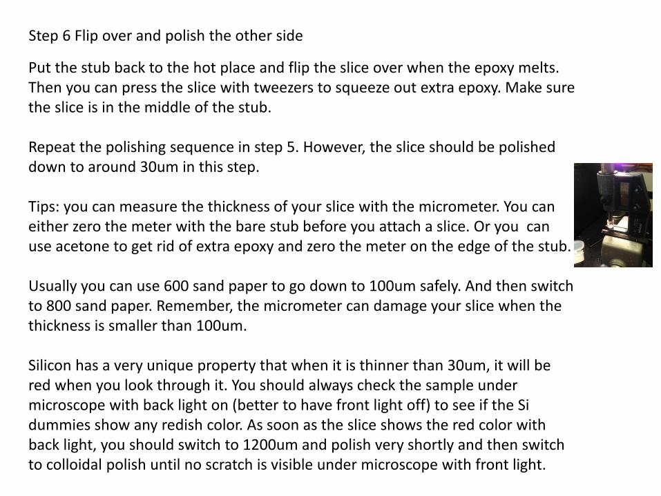
Put the stub back to the hot place and flip the slice over when the epoxy melts. Then you can press the slice with tweezers to squeeze out extra epoxy. Make sure the slice is in the middle of the stub. Repeat the polishing sequence in step 5. However, the slice should be polished down to around 30um in this step. Tips: you can measure the thickness of your slice with the micrometer. You can either zero the meter with the bare stub before you attach a slice. Or you can use acetone to get rid of extra epoxy and zero the meter on the edge of the stub. Usually you can use 600 sand paper to go down to 100um safely. And then switch to 800 sand paper. Remember, the micrometer can damage your slice when the thickness is smaller than 100um. Silicon has a very unique property that when it is thinner than 30um, it will be red when you look through it. You should always check the sample under microscope with back light on (better to have front light off) to see if the Si dummies show any redish color. As soon as the slice shows the red color with back light, you should switch to 1200um and polish very shortly and then switch to colloidal polish until no scratch is visible under microscope with front light.
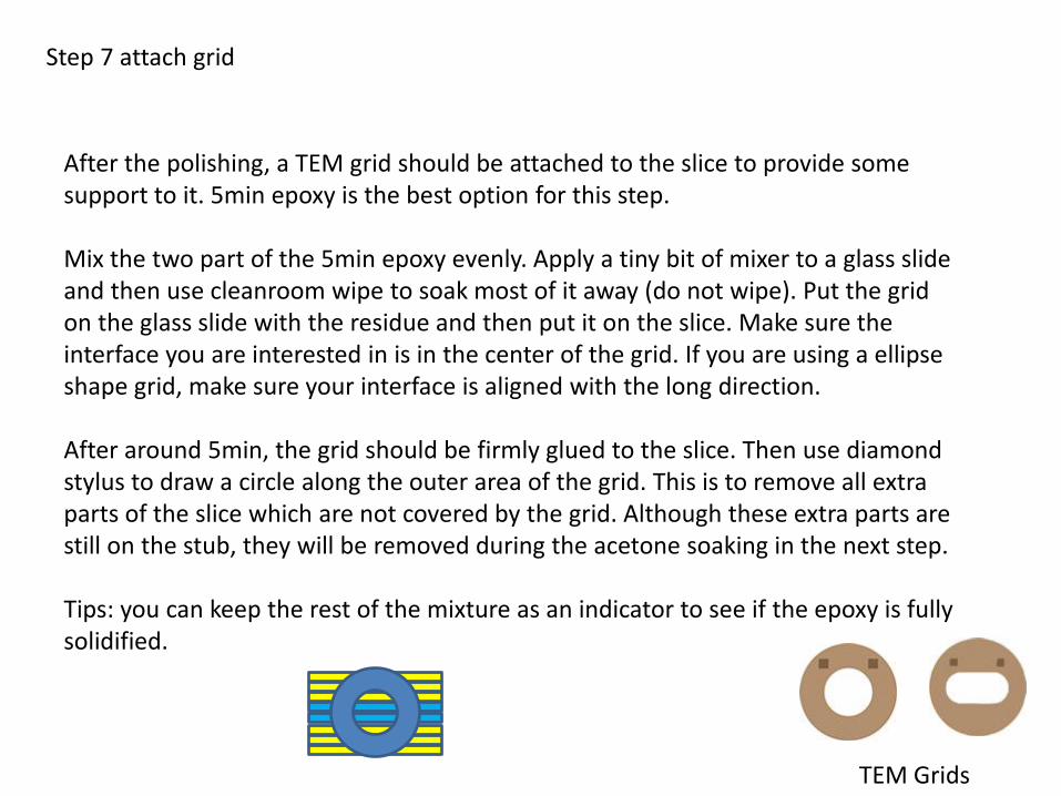
Step 7 attach grid
After the polishing, a TEM grid should be attached to the slice to provide some support to it. 5min epoxy is the best option for this step. Mix the two part of the 5min epoxy evenly. Apply a tiny bit of mixer to a glass slide and then use cleanroom wipe to soak most of it away (do not wipe). Put the grid on the glass slide with the residue and then put it on the slice. Make sure the interface you are interested in is in the center of the grid. If you are using a ellipse shape grid, make sure your interface is aligned with the long direction. After around 5min, the grid should be firmly glued to the slice. Then use diamond stylus to draw a circle along the outer area of the grid. This is to remove all extra parts of the slice which are not covered by the grid. Although these extra parts are still on the stub, they will be removed during the acetone soaking in the next step. Tips: you can keep the rest of the mixture as an indicator to see if the epoxy is fully solidified.
TEM Grids
Step 8 soak with Acetone
Wrap the stub with a filter paper and soak it into a small beaker of acetone. It usually takes 1h to overnight for the slice to detach(depends on how hard you squeezed the crystal bond epoxy). Then take slice out with tweezers (carefully, only touch the grid covered part). Optional: You can attach another grid on the other side of the slice to provide even more support. But the handling is a little bit challenging and a lot of times it will destroy your sample.
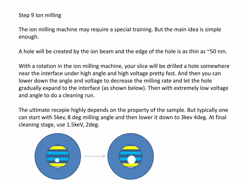
Step 9 Ion milling
The ion milling machine may require a special training. But the main idea is simple enough. A hole will be created by the ion beam and the edge of the hole is as thin as ~50 nm. With a rotation in the ion milling machine, your slice will be drilled a hole somewhere near the interface under high angle and high voltage pretty fast. And then you can lower down the angle and voltage to decrease the milling rate and let the hole gradually expand to the interface (as shown below). Then with extremely low voltage and angle to do a cleaning run. The ultimate recepie highly depends on the property of the sample. But typically one can start with 5kev, 8 deg milling angle and then lower it down to 3kev 4deg. At final cleaning stage, use 1.5keV, 2deg.
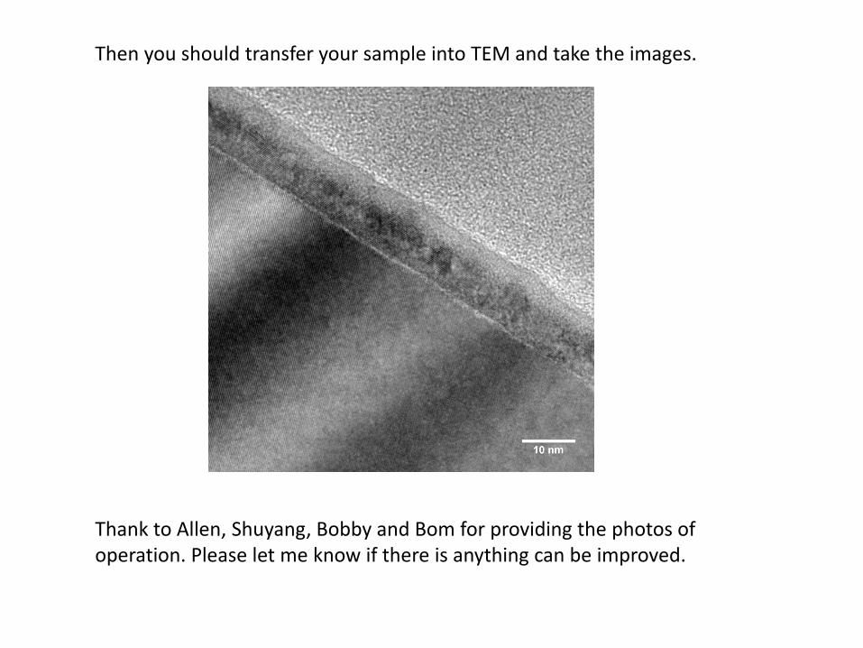
Then you should transfer your sample into TEM and take the images.
Thank to Allen, Shuyang, Bobby and Bom for providing the photos of operation. Please let me know if there is anything can be improved.