Embed Size (px)
Citation preview

University of ConnecticutOpenCommons@UConn
Doctoral Dissertations University of Connecticut Graduate School
12-18-2015
Temperature Dependent Characterization andCrystallization Dynamics of Ge2Sb2Te5 ThinFilms and Nanoscale StructuresKadir CilUniversity of Connecticut - Storrs, [email protected]
Follow this and additional works at: https://opencommons.uconn.edu/dissertations
Recommended CitationCil, Kadir, "Temperature Dependent Characterization and Crystallization Dynamics of Ge2Sb2Te5 Thin Films and NanoscaleStructures" (2015). Doctoral Dissertations. 943.https://opencommons.uconn.edu/dissertations/943
Temperature Dependent Characterization and Crystallization
Dynamics of Ge2Sb2Te5 Thin Films and Nanoscale Structures
Kadir Cil, Ph.D.
University of Connecticut, 2015
Phase change memory (PCM) is currently seen as the most promising candidate
for a future storage-class memory with the potential to be as fast as Dynamic Random-
Access Memory but with much longer retention times, and as dense as flash memory but
significantly faster due to unique material properties which include strong electrical
resistivity contrast, fast crystallization and high crystallization temperature. PCM devices
utilize chalcogenide materials (most commonly Ge2Sb2Te5, or GST) that can be
reversibly and rapidly switched between amorphous and crystalline phases (enabling
storage of information) with orders of magnitude difference in electrical resistivity.
Crystallization dynamics, transition temperatures, and grain size distributions depend on
the material composition, interfaces and cell geometry and determine the electrical pulses
required for operation, cell performance, power consumption and reliability.
This work focused on temperature dependent characterization of GeSbTe thin
films and nanoscale structures with the goal of contributing to a better understanding of
phase-change memory materials and devices.
The electrical resistivity of liquid GST (ρGST-Lq ) was extracted from
measurements on large number of individual GST nanostructures self-heated to melt by
single microsecond voltage pulses, as well as on thin film samples.The crystallization
behavior of GST films on silicon nitride and on silicon dioxide through slow resistance

versus temperature measurements was also characterized. Silicon nitride appears to
facilitate the fcc-hcp phase-transition of GST and we speculate this may be due to the
hexagonal symmetry of silicon nitride. Our results also show the importance of the
heating rate in determining phase transition temperatures.
Understanding the crystallization dynamics is critically important for PCM device
operation. Above a certain amplitude, a baseline (or offset) voltage after a melting pulse
can play an important role in the set operation by leading to retention of a molten
filament and growth-from-melt templated from the surrounding crystalline regions. The
effect of different baseline voltages on the set dynamics of phase change memory devices
was studied by applying melting voltage pulses with varying baseline voltages.
Simulations of the effect of different baseline voltages were also performed to compare to
and help interpret the experimental results.
Lastly, in-situ X-Ray Diffraction (XRD) measurements up to high temperatures
and ex-situ XRD measurements on pre-annealed samples were performed to characterize
grain size distributions as a function of anneal temperature. The material crystallizes over
time as the chuck temperature is increased and the crystallization process is monitored by
the evolution of different peaks in the XRD measurement which are related to the grain
sizes. These results will be used to improve and calibrate our electrothermal and
crystallization models for PCM materials and devices.
Kadir Cil - University of Connecticut, 2015

iii
Temperature Dependent Characterization and Crystallization
Dynamics of Ge2Sb2Te5 Thin Films and Nanoscale Structures
Kadir Cil
M.S., University of Connecticut, 2011
A Dissertation
Submitted in Partial Fulfillment of the
Requirements for the Degree of
Doctor of Philosophy
at the
University of Connecticut
2015

v
Acknowledgments
I would like to thank my mother Sultan and my father Akif for their support,
belief and patience throughout my education over the years. I would also like to thank my
dear wife Nevin for encouragement and motivation and my little daughter Sena Beyza
who joined our family on the last year of my Ph.D.
I am grateful and would like to thank my major advisors Prof. Helena Silva and
Prof. Ali Gokirmak for their guidance and mentorship, and also friendship throughout my
M.S. and Ph.D. programs; spending their valuable time inside and outside the lab and
building a very comfortable and friendly research environment; opening their house,
cooking meals and spending time together with our lab group and their three daughters
Sofia, Aida and Mina who have joined us over the years of my Ph.D.
I would also like to thank my other committee members, Prof. Rajeev Bansal,
Prof. Radenka Maric and Prof. Ali Bazzi for their valuable feedback and suggestions on
my thesis work.
During my Ph.D. I met really talented people, professionally and personally. I
would like to thank my former and current labmates: Gokhan Bakan for his help on lab
training and on measurement setups, and being my roommates for 3.5 years; Mustafa
Akbulut for his big solutions in the lab and simulation tool training; Faruk Dirisaglik for
his help and being my roommate for 1.5 years; Lhacene Adnane for his great hands-on
talent and contributions to our lab; Sadid Muneer for his help on Matlab programs and
proof readings; Nafisa Noor, Zachary Woods, Azer Faraclas and Jake Scoggin for their
valuable help and support on simulations; Maren Wenberg, Adrienne King, Zoila Jurado,

vi
Lindsay Sullivan and Jonathan Rarey, for their help on measurements; Adam Cywar,
Nicholas Williams, Abdiel Rivera, Sencer Ayas, Luca Lucera, Austin Deschenes and
Nabila Adnane for their help and friendship in the lab. I would like to thank Mustafa
Akbulut, Faruk Dirisaglik and Adam Cywar again for the fabrication of the GST thin
films and devices in IBM T.J. Watson Research Center. I would like to thank each of
them individually for their perfect friendship and support over the years to complete my
Ph.D.
I also would like to thank my friends outside the lab: Murat Osmanoglu, Ahmet
Teber, Yusuf Albayram, Halit Dogan, Abdurrahman Arikan, Sadullah Yildirim, Omer
Dis, Muammer Avci, Ozgur Oksuz, Hakan Gokmuharremoglu, Huseyin Yer, Turgut
Yilmaz, Ridvan Umaz for their support and very warm friendship environment.
I would like to thank Dr. Chung Lam, Dr. Yu Zhu and Dr. Jing Li from IBM for
their support and help on device fabrication and Dr. Bill Willis from Chemistry
department at UConn for his help with the SAM measurements.
Last but not least I would like to acknowledge a graduate fellowship from the
Republic of Turkey Ministry of National Education.

vii
Table of Contents
Table of Contents .............................................................................................................. vii
List of Figures .................................................................................................................... iii
1. Introduction ................................................................................................................. 1
1.1 Material parameters for phase change memory device modeling ........................ 3
2. Electrical Resistivity of Liquid GST ........................................................................... 8
2.1 Thin Film Measurements ................................................................................... 11
2.2 Device Level Measurements .............................................................................. 11
2.3 Results and discussion ........................................................................................ 16
3. Assisted cubic to hexagonal phase transition in GeSbTe thin films on silicon
nitride ................................................................................................................................ 20
3.1 Introduction ........................................................................................................ 20
3.2 Experimental details ........................................................................................... 21
3.3 Scanning Auger Microscopy (SAM) measurements .......................................... 25
3.4 Results and Discussion ....................................................................................... 30
4. The Effect of a Baseline Voltage on Crystallization of Nanoscale Ge2Sb2Te5
Devices .............................................................................................................................. 37
4.1 Constant Baseline Voltage Before and After Melting ....................................... 37
4.1.1 Experiments on GST Line Cells ................................................................. 37
4.1.2 Simulations of GST Line Cells ................................................................... 41
4.1.3 Simulations of GST Pore-like Cells ............................................................ 44

viii
4.2 Decreasing Baseline Voltage after Melting ....................................................... 49
4.2.1 Experiments on GST Line Cells ................................................................. 49
4.2.2 Simulations on GST Line Cells .................................................................. 51
4.3 Summary ............................................................................................................ 54
5. In-situ and ex-situ XRD measurements of GeSbTe thin films at various annealing
temperatures ...................................................................................................................... 56
5.1 Introduction ........................................................................................................ 56
5.2 XRD Measurements ........................................................................................... 56
5.3 Finite Element Simulations ................................................................................ 60
6. Conclusion ................................................................................................................. 63
7. Appendices ................................................................................................................ 66
7.1 Software tools developed using LabVIEW for instrument control for
electrical characterization .............................................................................................. 66
7.1.1 Pulse generator control program ................................................................. 66
7.1.2 Oscilloscope data acquisition program ....................................................... 67
7.1.3 Cryogenic probe station and temperature controller data acquisition
program ..................................................................................................................... 68
7.1.4 Semiconductor parameter analyzer control program .................................. 69
7.1.5 Semiconductor parameter analyzer data plot and analysis program ........... 71
7.1.6 Function generator unit control program .................................................... 73
7.1.7 Oscilloscope data acquisition program ....................................................... 74

ix
7.2 Optical band gap measurement for amorphous GST thin film .......................... 76
7.3 Scanning Auger Microscope Setup .................................................................... 78
8. References ................................................................................................................. 82

iii
List of Figures
Figure 1.1. Temperature dependent electrical and thermal conductivities of TiN (a),
thermal boundary conductivities between GST-SiO2, GST-TiN and TiN-SiO2
(b), electrical resistivities of amorphous and fcc GST (c), thermal conductivity
of GST (calculated electronic and estimated phonon contributions) (d), Heat
capacity of GST around the melting temperature (e), inset showing the peak to
incorporate the latent heat of fusion, and Seebeck coefficient of amorphous and
fcc GST (f)[15, 16, 23, 24, 30, 32] ......................................................................... 6
Figure 2.1. Simulated mushroom phase-change memory device and the two distinctly
different simulated temperature profiles, using the two previously reported
values for electrical resistivity of liquid GST (ρGST-Lq ~ 0.4 mΩ.cm [33] and ~
4 mΩ.cm [34]). Temperature-dependent materials parameters, latent heat of
fusion upon melting, thermoelectric contributions and thermal boundary
resistances are included in this model [15, 23]. The lowest temperature is 300
K. The white contour lines indicate the solid-liquid transition temperature
range (assumed as 873-883 K), within which GST is in the liquid state. ............... 9
Figure 2.2. Resistivity of a 100 nm thick amorphous GST film, measured up to 900 K.
The sudden increase at 900 K indicates losing contact with the film. The
arrows indicate transitions from amorphous to fcc (T1 ~ 428 K), from fcc to
hcp (T2 ~ 637 K) and from hcp to liquid (melting ~ 858 K). Inset SEM image
shows a segment of a 100 nm thick GST film which has been heated up to 875
K. The GST film breaks apart in liquid phase, possibly due to surface tension
and form hexagonal boundaries upon resolidification. ......................................... 10

iv
Figure 2.3. Resistivity as a function of temperature for an L x W x t = 460 nm x 160
nm x 50 nm pulse-amorphized GST line-cell (using 500 ns, 2.2 V, at room
temperature) and an as-fabricated fcc GST line-cell L x W x t = 460 nm x 255
nm x 50 nm. The arrows indicate transition temperatures from amorphous to
fcc (T1 ~ 420 K) and from fcc to hcp (T2 ~ 640 K). .............................................. 13
Figure 2.4. Schematics of the fabrication processes of the GST line structures on 700
nm SiO2 grown on Si (a), after 250 nm deep trench formation (b), 300 nm TiN
fill (c), CMP (d), GST film deposition (e), patterning of GST film (f), and
Si3N4 cap layer deposition (g). SEM image of a fabricated line structure (h)
and the schematic of the experimental setup (i).................................................... 14
Figure 2.5. Measured voltage (VA), current (VB/50 Ω) and total resistance (RT) as a
function of time for an L x W x t = 615 nm x 180 nm x 20 nm GST line.
T=500 K. I(t) and V(t) data are smoothed using a 1,000 point adjacent
averaging. After the pulse the line is amorphized and the current levels are too
low to be accurately measured by the oscilloscope due to significant voltage
offsets [37]. The actual resistance is expected to be 10x higher than what could
be measured. The baseline voltage used to measure resistance leads to
sufficient current flow and self-heating to keep the wire above ambient
temperature, hence resistance in amorphous state is observed to be increasing
gradually after the melting pulse. The metastable amorphous state is
significantly more conductive at elevated temperatures. Crystallization time at
500 K is ~1000 s [38] and recrystallization of the wire is not captured in the 20
microsecond duration of this measurement. ......................................................... 15
v
Figure 2.6. GST resistance (RGST) during pulse versus reciprocal of line width in
logarithmic scales for 4 different L, for t = 20 nm (W = 60 to 420 nm in 20 nm
increments), t = 50 nm (W = 100 to 600 nm in 20 nm increments). Inset shows
the L = 535 nm and linear fits for both thicknesses. ............................................. 18
Figure 2.7. Slopes (α) obtained from the fits in Fig. 6 versus L and linear fits for two
different thicknesses (20 and 50 nm) of GST lines............................................... 19
Figure 3.1. Schematics of a GST/nitride sample with contact pads used for two-point
R-T measurements (a) and a GST/oxide sample directly probed for four-point
R-T measurements (the probes can easily scratch the 10 nm capping silicon
dioxide) (b). Films, contact pads and probes are not drawn to scale for
visibility. The GST films are 10, 20, 50 or 100 nm and the underlying silicon
dioxide and silicon nitride are 300 nm and 50 nm respectively. .......................... 22
Figure 3.2. Perkin Elmer PHI 670 Scanning Auger Microscope (SAM). ........................ 25
Figure 3.3. Electron detector map image for the 50 nm GST film on SiO2 substrate. ..... 26
Figure 3.4. The full survey spectrum for the 10 nm GST film on SiO2 substrate, along
with element concentrations. ................................................................................ 26
Figure 3.5. Atomic concentration as a function of Ar+ sputter time for GST films of 20
nm thickness on SiO2 (left) and on Si3N4 (right). ................................................. 27
Figure 3.6. Atomic concentration as a function of Ar+ sputter time for GST films of 50
nm thickness on Si3N4 (left) and on SiO2 (right). ................................................. 28
Figure 3.7. Atomic concentration of Sb as a function of Ar+ sputter time for 100 nm
GST films to show the use of the sigmoidal curve and the asymptotes in
determining values of time.................................................................................... 29
vi
Figure 3.8. Atomic concentration of elements as a function of film depth for GST
films of 100 nm thickness on SiO2 (left) and on Si3N4 (right).............................. 29
Figure 3.9. Resistivity as a function of temperature for Ge2Sb2Te2 films on silicon
nitride and silicon dioxide starting as amorphous (as-fabricated) showing phase
transitions from amorphous to fcc and from fcc to hcp at T1 and T2
respectively. Resistivity is extracted from resistance measurements using two-
point measurement with platinum contacts or four-point measurements using
tungsten tips directly probing the GST films. For the thinnest film (10 nm) on
silicon nitride the second transition is not observed as the resistance starts
increasing before the expected transition temperature, possibly due to film
segregation into discontinuous regions. ................................................................ 31
Figure 3.10. Scanning Electron Microscopy image of the 10 nm thick GST/nitride
sample after the R-T measurement up to ~ 600 K. The resistance started
increasing at ~ 540 K, likely due to the observed segregation of the film into
discontinuous regions near the metal pads. ........................................................... 32
Figure 3.11. GST phase transition temperatures T1 (amorphous to fcc) and T2 (fcc to
hcp) as a function of film thickness obtained from various measurements on
both GST/oxide (T1 ◊, T2 ) and GST/nitride (T1 T2 Δ ) samples. For the
GST/nitride samples large area contact pads were used for 2-point R-T
measurements. For the GST/oxide samples tungsten probe tips were used for
4-point measurements. In all 50 nm GST/oxide samples the GST film was
patterned by deposition through a contact mask. One of the 50 nm thick
GST/nitride samples () was measured using tungsten tips to directly probe the

vii
GST film (4-point measurement). The 100 nm thick GST/nitride sample was
measured with similar size contacts (~ 1 mm x 1 mm) formed using graphite
paste. The transition temperatures are extracted as the point at which the first
derivative reaches the two local minima. .............................................................. 33
Figure 3.12. Room temperature resistivity for all thickness films on GST/nitride and
GST/oxide samples, in amorphous, cubic and hexagonal phases. The fcc and
hcp GST films on GST/oxide sample are obtained by heating as-deposited
amorphous films to 565 K or 670 K (above the first or second transition)
followed by cooling to room temperature for resistivity measurements. GST
films on GST/nitride samples are deposited as amorphous, fcc or hcp. ............... 34
Figure 3.13. Phase transition temperatures observed from resistance versus
temperature measurements (R-T) with heating rates of 1 K/min and 5 K/min on
GST films of various thicknesses on GST/oxide (left) and GST/nitride (right)
samples. ................................................................................................................. 36
Figure 4.1. Applied voltage pulses (a) and measured current (b) with offset voltages
varying from 1.4 V to 1 V on a Length: 350 nm Width: 72 nm device. Circuit
schematic of the experimental setup (inset a) and load resistors attached on
probe tips (inset b). ............................................................................................... 39
Figure 4.2. Measured current signals on a GST wire with varying offset voltages (1.5
V to 1.2 V) (a), with different offset voltages (b) to show the effect of offset
voltage by switching between amorphous and crystalline phases. ....................... 40

viii
Figure 4.3. Schematics of a fabricated line cell structure with contact pads (a). SEM
image of a fabricated line cell (b) Cross section of the simulated line cell
geometry and materials (c).................................................................................... 42
Figure 4.4. Output currents (a), and calculated resistances (b) with varying baseline
voltages on simulated (Length 400 nm, Diameter 94 nm) GST line cell. Output
currents (c), and calculated resistances (d) with varying baseline voltages on
simulated (30 nm thick, Diameter 200 nm) GST pore-like structure. .................. 43
Figure 4.5. Schematic of the simulated pore-like structure PCM cell (a). Applied
voltage as a function of time ( are indicate at the end of the main pulse and at
the end of the simulation) (b). Measured current through the GST cell (c). ......... 44
Figure 4.6. Temperature profile of the simulated pore-like structure PCM cell (200 nm
diameter GST) using the four different baseline voltages (Figure 1c). Images
are captured at the end of the main pulse and at the end of the simulation
(indicated in Figure 1b). ........................................................................................ 46
Figure 4.7. The maximum temperature reached as a function of offset voltage at the
end of the simulation (30 ns). ............................................................................... 47
Figure 4.8. Simulated current through various diameters GST cells (height of 30 nm)
for different baseline voltages. .............................................................................. 48
Figure 4.9. Maximum temperature reached within different diameter GST cells for
different baseline voltages as a function of simulation time................................. 49
Figure 4.10. Applied voltage and output current (as shown in the measurement setup
in Figure 4.1 a inset), and calculated resistance of the GST line cell (Length
400 Width 140 nm and thickness 50 nm). ............................................................ 51

ix
Figure 4.11. Cross section of the simulated line cell geometry and materials. A resistor
is added in series to limit the current (a). 3D sliced view of the simulated cell
(b). ......................................................................................................................... 52
Figure 4.12 Simulated applied voltage waveform and output current (a) and resistance
and molten volume (b) of the simulated GST line cell (length 360 nm, diameter
50 nm). (c) and (d) show a ‘zoomed-in’ view of the same data in the period
after the melting pulse. .......................................................................................... 53
Figure 4.13. Temperature and crystalline density profiles of the GST wire during the
simulation, at given simulation times. The white areas indicate the molten
regions (T > 873 K). ............................................................................................. 54
Figure 5.1. X-ray intensity peak from GST thin film at 300 oC. The Scherrer equation
is used to calculate average grain size where K is the dimensionless shape
factor (~0.9-1), λ is the X-ray wavelength. Peak width (β) which is Full Width
Half Maximum (FWHM) value inversely proportional to crystallite size (L)
(a). In-situ XRD patterns of 200 nm thick GST thin film at various chuck
temperature (b). ..................................................................................................... 58
Figure 5.2. In-situ XRD measurement temperature as a function of time up to 400 oC,
in 2 oC/min (a) and 700 oC, in decreasing heating rate (5, 2 and 0.5 oC/min) (b).
Flat temperature regions are ~ 34 minutes and correspond to the XRD scanning
time. ...................................................................................................................... 58
Figure 5.3. Average grain sizes (calculated from in-situ XRD data) and resistances of a
different 200 nm thick GST film sample with corresponding phases as a
function of chuck temperature (a). Average grain sizes of 200 nm thin film

x
GST with nucleation rate and growth velocity [73] of GST as a function of
temperature. Grain sizes are jumping where nucleation rate (also phase change
from fcc to hcp) and growth velocity are maximized. .......................................... 59
Figure 5.4. Room temperature resistivity and average grain size as a function of
anneal temperature for 100 and 200 nm thickness GST films (a). Average grain
sizes of two 200 nm films calculated from in-situ XRD measurements
(squares) and of 100 nm and 200 nm calculated from (ex-situ) XRD
measurements (circle and diamonds) after pre-annealing at the given
temperatures (x-axis) for 15 min (b). .................................................................... 60
Figure 5.5. Cross section of the planar mushroom cell geometry and materials
simulated using COMSOL multiphysics with the electrothermal and CD
models mentioned earlier [70] (a). GST region of (20 nm depth) planar
mushroom cell with varying crystalline size after 200 ns annealing at 300 oC
(b), 350 oC (c), and 400 oC (d). In these simulations the device is annealed at
different constant temperatures from t=0 to t=200 ns. .......................................... 61
Figure 5.6. Average grain size as a function of anneal temperature obtained from in-
situ XRD data for a 200 nm thick GST thin film, ~ 34 minutes at each
temperature (solid circles) and from preliminary simulations on GST cells
annealed at various, constant anneal temperatures for 200 ns (open circles). ...... 62
Figure 7.1. Front panel of pulse generator controller tool. .............................................. 66
Figure 7.2. Front panel of Tektronix DPO 4104 Oscilloscope data acquisition tool........ 67
Figure 7.3. Front panel of Janis UHT-500 cryogenic probe station and temperature
controller data acquisition tool.............................................................................. 69

xi
Figure 7.4. Front panel of Agilent 4156C semiconductor parameter analyzer control
tool. ....................................................................................................................... 71
Figure 7.5. Front panel of semiconductor parameter analyzer data plot and analyzer
tool. ....................................................................................................................... 72
Figure 7.6. Front panel of Tektronix AFG-3102 function generator control tool. ........... 74
Figure 7.7. Front panel of Tektronix DPO-4104 oscilloscope data acquisition tool. ....... 75
Figure 7.8. Optical reflection spectrum of the 100 nm amorphous GST thin film in
200-1600 nm wavelength range. ........................................................................... 76
Figure 7.9. Plotting based on the relationship of [hν ln (Rmax-Rmin)/(R-Rmin)] 2 and hν
for 100 nm amorphous GST thin film. The intercept in the abscissa indicates
an optical band gap of 1.16 eV (inset). ................................................................. 77
Figure 7.10. Fitting based on the relationship of [hν ln (Rmax-Rmin)/(R-Rmin)] 2 and hν
for 100 nm amorphous GST thin film. 1.16 eV is determined as optical band
gap of the amorphous GST film............................................................................ 78
Figure 7.11. Auger depth profiling schematics. ................................................................ 79
Figure 7.12. SEM images of the pulsed GST device (Width: 96 nm and Length: 220
nm). 100 x 100 µm contact pads are shown in top figure. Higher magnification
SEM images shows the metal contact (middle figure) and GST device (bottom
figure). ................................................................................................................... 80
Figure 7.13. Janis UHT-500 cryogenic probe station with turbo pump. Full HD
camcorder attached with optical lens and TV are used for positioned the
micromanipulator probes. ..................................................................................... 81

xii
Figure 7.14. Inside of the vacuum chamber and the radiation shield of the cryogenic
probe station. Micromanipulators with triaxial probe connections,
thermocouples and silicon diode sensor attached to the chuck are shown. .......... 81

1
1. Introduction
Demand for high-speed, high-density and low-power computation, and
expected limitations in scaling of silicon based memory technologies have given rise
to investigation of alternative complementary memory technologies such as phase
change memory (PCM). PCM is currently seen as one of the most promising
candidates for a future storage-class memory [1] with the potential to be almost as fast
as Dynamic Random-Access Memory but with much longer retention times (non-
volatile), and as dense as flash memory but significantly faster. A possible non-
volatile DRAM replacement (no need for refresh and data stored without power
supplied) is especially interesting and it could lead to completely new computer
architectures. Meanwhile, NAND flash has successfully continued scaling to < 20 nm
gate length and 3D V-NAND (with vertical integration of 32 layers of planar NAND)
is now being produced by Samsung [2]. PCM has recently entered the market as a
lower-density but significantly higher-speed non-volatile memory for mobile
applications [3, 4]. PCM’s advantage of single bit alterability over flash memory
(which requires block-erase to rewrite) makes it a lower-power alternative for certain
applications such as code execution [5]. Storage class memory applications such as
server and hard drive replacement, require high endurance (number of cycles) while
maintaining the fast switching [6]. PCM has much lower latency and higher endurance
than NAND flash (106 for PCM and ~ 3 x 10⁴ NAND flash) which makes it a well-
positioned candidate for server and storage systems where a small amount of PCM can
be integrated (hybrid structure) to the speed of the system [7].

2
Current pulses for the set and reset operations are provided through access
device (transistors, diodes) which typically need to be larger than the PCM element
itself to provide sufficient current and thus limit the memory packing density. One of
the goals to optimize cell design is to reduce the reset current which leads to reduced
size of access device, larger storage density and also higher cycling (reduced material
damage from lower currents). PCM devices are expected to scale below 10 nm element
size with potential for multi-bit/cell storage [8, 9] making PCM promising for non-
volatile random access memory implementations if the cells can be operated reliability
for very large number of cycles [10].
PCM devices utilize chalcogenide materials (most commonly GeSbTe, or GST
[11]) that can be reversibly and rapidly switched between amorphous and crystalline
phases with orders of magnitude difference in electrical resistivity. A typical PCM
device (mushroom cell) consists of a thin layer of a phase-change material sandwiched
between a narrow bottom contact (usually referred to as the heater) and a planar top
contact. The active region is a GST semi-sphere above the heater that is switched
between the amorphous and crystalline states by a suitable electrical pulse.
Amorphization is obtained by a large amplitude and short electrical pulse that heats the
active region above its melting temperature and allows it to cool faster than the
crystallization time to re-solidify as amorphous. Crystallization can be obtained by a
smaller amplitude and longer duration pulse that heats the active region above its
crystallization temperature (Tcryst) for a sufficiently long period. Fast crystallization can
also be obtained at high temperatures, close to melting, or upon slower cooling from
melting. Since the resistivity of the amorphous region is very large, sufficient current

3
flow for Joule heating and crystallization is obtained with voltage pulses that are high
enough to initiate electrical breakdown (threshold switching). In GST films, the room-
temperature electrical resistivity changes by a factor of ~ 105-106 between the
amorphous and crystalline phases Viable PCM operation and scaling require melting of
a very small volume of phase-change material in a very short time period with
minimum possible energy, while ensuring reliability over the lifetime of the device and
a large number of melting and solidification cycles (~109) [7]. Operation of the PCM
cell also depends on the choices of the substrate and thickness of the phase change
material. We have compared the crystallization behavior of GST films on different
substrates with varying GST film thickness under different heating rates. The
measurements demonstrate that crystallization temperature can increase or decrease
depending on substrate material and film thickness and the difference can be as large as
80 K for second transition temperature (from fcc to hcp). Ge2Sb2Te5 (GST) is the most
common phase change material due to its crystallization times, stability of amorphous
phase and large resistivity contrast between the amorphous and crystalline phases [12].
In small-scale PCM devices, in which the active region is repeatedly switched between
amorphous and face-centered cubic (fcc) phases, an overall resistance ratio of ~ 100-
1,000 is typically obtained with switching times ~ 50-100 ns[11].
1.1 Material parameters for phase change memory device modeling
PCM elements experience large range of operation temperatures and thermal
gradients (~10-100 K/nm) while switching between crystalline, liquid and amorphous
phases. Crystallization is materialized by reorganization of atoms and bonding
mechanisms at the molecular level. Crystallization dynamics and transition

4
temperatures depend on the composition, interfaces and cell geometry and determine
the required electrical pulses used for operation, which in turn impact cell performance,
power consumption and reliability [13]. Rigorous device modeling that can enable
further scaling and evaluation of device failure mechanisms, requires well-determined
materials parameters in the whole operation range including the liquid state. The
temperature dependent material parameters used in the modeling studies shown in this
thesis are shown in Figure 1.1 [14-16].
Electrical resistivity (ρ) and thermal conductivity (κ) as a function of temperature
of TiN are obtained from Gottlieb et al. [17] and Shackelford et al. [18] respectively
(Figure 1.1a). Heat capacity and Seebeck coefficient of TiN are assumed to have constant
values of 784 J/kg.K and 1 µV/K. [19, 20].
Thermal boundary resistances (TBR) at the GST-TiN, GST-SiO2, and TiN-SiO2
interfaces are obtained by adding 1 nm thick virtual layer at each boundaries with a
temperature dependent thermal boundary conductivity (TBC). TBR at GST-TiN interface
is ~20 m2K/GW between 300 K and 600 K and it decreases significantly due to increased
electronic contribution of thermal conductivity when the phase change material
approaches melting temperature. TBR at GST- SiO2 interface is negligible up to melting
temperature of GST. When the GST melts and becomes highly conductive TBR increases
to ~20 m2K/GW, typical value for metal-insulator interface. TBC between TiN and SiO2
is assumed to be constant: 0.05 W/(m.K) as these materials do not change phase in that
temperature range (Figure 1.1b) [21, 22].
Temperature dependent electrical resistance of amorphized and fcc GST wires are
measured from 300 K up to 675 K with 1K/min heating rate. The resistivity values are
5
calculated by using actual device dimensions. Up to first crystallization temperature (~
420 K) crystallization time scale is comparable for slow measurements. At elevated
temperatures crystallization is faster and resistivity of the material becomes a function of
temperature and heating rate. Therefore, GST retains a metastable crystalline state during
reset operation because the heating rate is faster than crystallization time. The calculated
exponential decay of resistivity values for amorphous and fcc GST are extrapolated up to
melting temperature to model the metastable resistivity functions [15, 16, 23-26]. Liquid-
GST resistivity values used in the simulations are from the experimental results obtained
by Cil et al. [14] (Figure 1.1c).
Room-temperature values of the thermal conductivity (κ) of GST as obtained
from the literature are considered to be purely due to phonon conduction [22, 27-29].
This term is assumed to be decreasing linearly with GST resistivity, whereas the
electronic contribution is calculated to be increasing with temperature following the
Wiedemann-Franz law which relates the thermal conductivity and the electrical
conductivity of a metal. Total thermal conductivity is calculated as sum of the phonon
and electronic components. Thermal conductivity of liquid GST is assumed to be
dominated by the electronic conduction due to the large electrical conductivity (Figure
1.1d); contributions from convection in liquid phase are not accounted for [23].
The heat capacity (CP) of GST is obtained from both Yin et al. [19] and Liu et al.
[20] as a constant value of 202 J/(kg.K). Latent heat of fusion of GST is accounted for by
a 10 K spike in the heat capacity function for the heat required for solid to liquid phase-
change. A 10 K phase-change range is preferred for ease of simulations, instead of a
more sudden transition (Figure 1.1e).
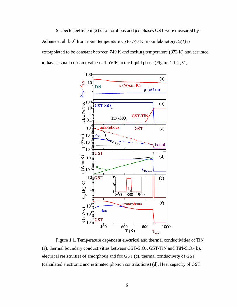
6
Seebeck coefficient (S) of amorphous and fcc phases GST were measured by
Adnane et al. [30] from room temperature up to 740 K in our laboratory. S(T) is
extrapolated to be constant between 740 K and melting temperature (873 K) and assumed
to have a small constant value of 1 µV/K in the liquid phase (Figure 1.1f) [31].
Figure 1.1. Temperature dependent electrical and thermal conductivities of TiN
(a), thermal boundary conductivities between GST-SiO2, GST-TiN and TiN-SiO2 (b),
electrical resistivities of amorphous and fcc GST (c), thermal conductivity of GST
(calculated electronic and estimated phonon contributions) (d), Heat capacity of GST

7
around the melting temperature (e), inset showing the peak to incorporate the latent heat
of fusion, and Seebeck coefficient of amorphous and fcc GST (f)[15, 16, 23, 24, 30, 32]
8
2. Electrical Resistivity of Liquid GST
Electrical resistivity of liquid Ge2Sb2Te5 is obtained from DC current-voltage
measurements performed on thin Ge2Sb2Te5 films as well as from device level micro-
second pulse voltage and current measurements performed on two arrays (thickness: 20 ±
2 nm, 50 ± 5 nm) of lithographically defined encapsulated Ge2Sb2Te5 nano/micro-wires
(length: 315 nm to 675 nm, width: 60 nm to 420 nm) with metal contacts. Thin film
measurements yield 1.26 ± 0.15 mΩ.cm (thickness: 50, 100 and 200 nm), however, there
is significant uncertainty regarding the integrity of the film in liquid state. The device
level measurements utilize melting of the encapsulated structures by a single voltage
pulse while monitoring the current through the wire. Melting is verified by stabilization
of current during the pulse. The resistivity of liquid Ge2Sb2Te5 is extracted as 0.31 ± 0.04
mΩ.cm and 0.21 ± 0.03 mΩ.cm from 20 nm and 50 nm thick wires arrays.
PCM utilizes the large electrical resistivity contrast between the amorphous and
the crystalline phases of phase change materials (typically chalcogenides [11]), which can
be reversibly and rapidly switched between the two phases by self-heating via electric
pulses. A typical PCM device (mushroom cell) consists of a thin layer of a phase-change
material sandwiched between a narrow bottom contact and a planar top contact (Figure
2.1). Amorphization is obtained by a large amplitude and short pulse which melts a small
semi-spherical volume of material covering the contact area and allows it to freeze
quickly. Crystallization is achieved by either using a smaller amplitude and longer
duration pulse which heats the amorphized region above the crystallization temperature
(Tcryst) for a sufficiently long period or melting followed by slower cooling. Since the
resistivity of the amorphous region is very large, sufficiently large voltage pulses are

9
needed to initiate electrical breakdown (threshold switching) for crystallization.
Figure 2.1. Simulated mushroom phase-change memory device and the two
distinctly different simulated temperature profiles, using the two previously reported
values for electrical resistivity of liquid GST (ρGST-Lq ~ 0.4 mΩ.cm [33] and ~ 4 mΩ.cm
[34]). Temperature-dependent materials parameters, latent heat of fusion upon melting,
thermoelectric contributions and thermal boundary resistances are included in this model
[15, 23]. The lowest temperature is 300 K. The white contour lines indicate the solid-
liquid transition temperature range (assumed as 873-883 K), within which GST is in the
liquid state.
300 K
≥1000 K
Tmax = 970 K Tmax = 1110 K
ρliq = 4 mΩ·cmρliq = 0.4 mΩ·cm
GST
Si Substrate
SiO2
100 x 100 nm
10 nm
15
0 n
m
TiN

10
Figure 2.2. Resistivity of a 100 nm thick amorphous GST film, measured up to
900 K. The sudden increase at 900 K indicates losing contact with the film. The arrows
indicate transitions from amorphous to fcc (T1 ~ 428 K), from fcc to hcp (T2 ~ 637 K) and
from hcp to liquid (melting ~ 858 K). Inset SEM image shows a segment of a 100 nm
thick GST film which has been heated up to 875 K. The GST film breaks apart in liquid
phase, possibly due to surface tension and form hexagonal boundaries upon
resolidification.
Even though GST is the most studied phase change material, at the time of this
publication there were only two reports on the electrical resistivity of liquid GST (ρGST-
Lq) in the literature (with significant disparity): ρGST-Lq ~ 4 mΩ.cm based on
measurements on a 110 nm thick GST film [34]; ρGST-Lq varying from ~ 0.41 mΩ.cm at
930 K to ~ 0.36 mΩ.cm at 990 K based on temperature dependent measurements on
molten GST (Tmelt = 873K ) in a macroscopic setup [33]. Thermal conductivity of liquid

11
GST (kGST-Lq) is expected to be dominated by its electronic component (metallic behavior)
and can be estimated using the ρGST-Lq value and Wiedemann-Franz (W-F) Law (kGST-Lq =
LT/ρGST-Lq, L = Lorenz Number). Similarly thermal boundary resistances (TBR) at liquid
GST interfaces with other materials are also estimated based on W-F Law and the ρGST-Lq
value [15]. Hence, the ~10x disparity in the reported values, which may be caused by
measurement errors, compositional differences, or thickness dependence, has a
significant impact on predicted device operation dynamics (Figure 2.1).
2.1 Thin Film Measurements
We have performed room temperature resistivity measurements using the Van der
Pauw method and four-point resistance versus temperature measurements on thin GST
films with patterned metal contacts (going above Tmelt) and obtained ρGST-Lq as 1.43
mΩ.cm for 50 nm, 1.14 mΩ.cm for 100 nm, 1.22 mΩ.cm for 200 nm thick films,
averaging 1.26 ± 0.15 mΩ.cm (Figure 2.2). We have observed that the films typically do
not maintain their integrity during the measurement, possibly due to surface tension, and
form hexagonal micro-structures upon resolidification, suggesting crystallization in
hexagonal close pack (hcp) phase (Figure 2.2 inset). Hence, thin film measurements are
not reliable enough to extract ρGST-Lq for rigorous device modeling and device level ρGST-
Lq measurements, in which the liquid can be contained, are necessary to verify the
reported values and determine if there are any size effects.
2.2 Device Level Measurements
The electrical measurements were performed in a Janis vacuum probe station [35]
with temperature control (up to 680 K), under high vacuum (10-5 torr) that minimizes

12
oxidation of the structures. The samples were clamped to the chuck for good thermal
contact and temperature was measured using an E-type thermocouple clamped to the
chuck. The slow (1 K/min ramp rate) R-T characteristics (300 K to 680 K) of an as-
fabricated wire (fcc) and a pulse-amorphized wire (at room temperature, using 500 ns, 2.2
V pulse) were simultaneously measured by continuously sweeping the applied voltages in
± 100 mV range using an Agilent 4156C semiconductor parameter analyzer (Figure 2.3).
The amorphous wire transitions to fcc phase at ~ 420 K (Tfcc) and both wires transition
from fcc to hexagonal-close-packed (hcp) phase at ~ 640 K (Thcp).
We have extracted ρGST-Lq from electrical pulse measurements [36] on a large
number of GST nano/micro-wires with bottom metal contacts fabricated using
conventional photolithography and semiconductor processing techniques on bulk Si
wafers with ~ 700 nm thermally grown SiO2 (Figure 2.4 a). 250 nm deep trenches were
etched into the SiO2 layer using reactive ion etching (RIE), which were filled with a 300
nm layer of titanium nitride (TiN) using chemical vapor deposition (CVD) and physical
vapor deposition (PVD) systems (Figure 2.4 b, c). The wafers were then polished using
chemical and mechanical polishing (CMP) to achieve planar bottom contacts (Figure 2.4
d). Undoped, stoichiometric Ge2Sb2Te5 films (20 ± 2 nm and 50 ± 5 nm) were deposited
by co-sputtering from elemental targets at low temperature (amorphous phase) (Figure
2.4 e), followed by sputter deposition of a 10 nm silicon dioxide (SiO2) cap layer. The
GST wire structures were then patterned using optical lithography and RIE (Figure 2.4 f)
with lengths (L) varying from 315 to 675 nm and widths (W) varying from 60 to 420 nm,
in 20 nm increments. A 15 nm silicon nitride (Si3N4) blanket layer is then deposited by
plasma-enhanced chemical vapor deposition (PECVD) at 200 ºC to encapsulate the

13
structures (Figure 2.4 g, h). Since the crystallization temperature of GST is ~ 150 ºC, the
structures are expected to transition from amorphous to fcc phase during this final
PECVD deposition step. The resulting device dimensions were measured by SEM.
Figure 2.3. Resistivity as a function of temperature for an L x W x t = 460 nm x
160 nm x 50 nm pulse-amorphized GST line-cell (using 500 ns, 2.2 V, at room
temperature) and an as-fabricated fcc GST line-cell L x W x t = 460 nm x 255 nm x 50
nm. The arrows indicate transition temperatures from amorphous to fcc (T1 ~ 420 K) and
from fcc to hcp (T2 ~ 640 K).

14
Figure 2.4. Schematics of the fabrication processes of the GST line structures on
700 nm SiO2 grown on Si (a), after 250 nm deep trench formation (b), 300 nm TiN fill
(c), CMP (d), GST film deposition (e), patterning of GST film (f), and Si3N4 cap layer
deposition (g). SEM image of a fabricated line structure (h) and the schematic of the
experimental setup (i).
Liquid state measurements (ρGST-Lq) were performed by melting the wires via self-
heating with short voltage pulses (Figure 2.5) since the chuck can only be heated to ~ 680
K < Tmelt = 873K. An Agilent 8114A pulse generator (PGU) and a Tektronix DPO4104
oscilloscope are configured as in Figure 2.4 (i) for the pulse measurements, using short
coaxial cables for connections. 1 to 1.9 V pulses with 1 µs duration and 0.2 V baseline
offset are applied to fully melt GST wires of varying sizes. Complete melting of the
structures is observed as a plateau in the current during the pulse (Figure 2.5)[36]. The
structures used in these measurements are narrow (~ 60-600 nm) and ~ 60% of the wires
are completely broken by the pulse after melting. The current levels are stable in the

15
liquid state prior to sudden breaking of the wires, which indicates that the wires are
completely molten and there is no molten filament that is widening or narrowing over
time. The baseline voltage is used to measure the wire resistance before and after the
pulse without significant self-heating. The sample temperature was kept at 500 K (> Tfcc)
to observe crystallization of the amorphized wires (after amorphization pulses) and verify
integrity of the structures.
Figure 2.5. Measured voltage (VA), current (VB/50 Ω) and total resistance (RT) as
a function of time for an L x W x t = 615 nm x 180 nm x 20 nm GST line. T=500 K. I(t)
and V(t) data are smoothed using a 1,000 point adjacent averaging. After the pulse the
line is amorphized and the current levels are too low to be accurately measured by the
oscilloscope due to significant voltage offsets [37]. The actual resistance is expected to be
10x higher than what could be measured. The baseline voltage used to measure resistance
leads to sufficient current flow and self-heating to keep the wire above ambient

16
temperature, hence resistance in amorphous state is observed to be increasing gradually
after the melting pulse. The metastable amorphous state is significantly more conductive
at elevated temperatures. Crystallization time at 500 K is ~1000 s [38] and
recrystallization of the wire is not captured in the 20 microsecond duration of this
measurement.
Self-heating in the melted region is limited due to reduced resistivity upon
melting and temperature stabilization at the liquid-solid interfaces at Tmelt due to
absorption of latent heat of fusion. The temperature variation within the melt is expected
to be small due to large electronic thermal conductivity in metallic liquid phase enhanced
by convection in liquid state [39]. Hence, the temperature of the melt is expected to
remain relatively close to Tmelt in these experiments. In addition, the reported temperature
coefficient of resistivity (TCR) of liquid GST from bulk measurements is small, ~ -0.8
μΩ.cm/K at 990 K[33], hence the variations in liquid state resistivity obtained by this
method due to the temperature rise within the molten volume are expected to be relatively
small.
2.3 Results and discussion
Figure 2.5 shows an example of the measured voltage (VA), output current (I = VB
/ 50Ω) and corresponding total resistance of a line cell (RT = (VA-VB) / I) during a 1 µs,
1.6 V pulse (L x W x t = 615 nm x 180 nm x 20 nm). The pulse voltage is constant after a
short transient period while the measured current has a characteristic non-linear response
until it reaches the maximum value (Figure 2.5). This non-linear behavior is expected to
be a combined effect of the negative temperature coefficient of resistance of GST and
dynamically changing power transfer conditions [40] as the structure starts melting. Once

17
a contact-to-contact liquid GST path forms, the resistance reaches a steady state (plateau)
and all reactive current contributions are eliminated. The measured total resistance (RT) at
the plateau includes the 50 Ω terminator, the TiN metal extension resistances (RM ≈ 200
Ω) and the GST wire resistance (RGST) (2.2). RGST includes Rx, the common contributions
arising from contact pads and TiN/GST interface contact resistance (2.2).
50MGSTT RRR (2.1)
XRWt
LRGST (2.2)
RT at the plateau is plotted as a function of 1/W for devices with different L
(Figure 2.6). The y-intercept of the linear fits made for each L indicate contact resistance
values common to all wires (Rx = 114 ± 32 Ω for t = 20 nm and 98 ± 27 Ω for t = 50 nm).
The slopes of these fits (α = .L/t) are then plotted as a function of L for both thicknesses
Figure 2.7). The slopes of these second fits ( = /t) are used to extract the liquid state
resistivity, ρGST-Lq, as 0.31 ± 0.04 mΩ.cm for t = 20 nm and 0.21 ± 0.03 mΩ.cm for t = 50
nm. The calculated errors have contributions from the error in regression for , which
accounts for the error in regression for α values (shown as error bars in Figure 2.7) and
the error in thickness (estimated as ~ 10% based on SEM imaging). The difference
between the results obtained from 20 nm and 50 nm thick structures may be due to
variations in the melting of the wider pad region, impact of pressure or surface cooling
effects for the two thicknesses.
The extracted values of 0.31 ± 0.04 mΩ.cm and 0.21 ± 0.03 mΩ.cm from 20 nm
and 50 nm thick structures using this device level approach are close to those reported by

18
Endo et al. from large-scale measurements of liquid GST (~ 0.36 mΩ.cm at ~ 990 K with
a TCR of -0.8 μΩ.cm/K [33]). This extracted liquid resistivity value is also comparable to
resistivity of the hcp phase at melting temperature (Figure 2.2).
Figure 2.6. GST resistance (RGST) during pulse versus reciprocal of line width in
logarithmic scales for 4 different L, for t = 20 nm (W = 60 to 420 nm in 20 nm
increments), t = 50 nm (W = 100 to 600 nm in 20 nm increments). Inset shows the L =
535 nm and linear fits for both thicknesses.

19
Figure 2.7. Slopes (α) obtained from the fits in Fig. 6 versus L and linear fits for
two different thicknesses (20 and 50 nm) of GST lines.

20
3. Assisted cubic to hexagonal phase transition in GeSbTe thin films
on silicon nitride
The amorphous to face-centered cubic (fcc) and fcc to hexagonal close-packed
(hcp) crystallization temperatures of GeSbTe thin films on underlying silicon nitride
and silicon dioxide films were studied through slow (1 K/min) resistance versus
temperature measurements. The amorphous to fcc phase transition is observed at ~ 170
oC for both cases but the fcc to hcp phase transition temperature for GeSbTe films on
silicon nitride is observed ~ 80 oC lower than for GeSbTe films on silicon dioxide,
possibly due to the hexagonal symmetry of silicon nitride.
3.1 Introduction
The crystallization behavior of the phase change material determines the power
required for switching, programming speed, retention time and also affects other
important device properties such as reliability and device-to-device variability. It has
been observed that the crystallization behavior of phase change materials depends
strongly on chemical composition [41], structure, heating rate [42], cladding materials
[43], doping, and even thickness or device size [12]. GST undergoes a first phase
transition from amorphous to fcc and a second phase transition from fcc to hexagonal
close-packed (hcp) [44]. Most research to date has focused on the amorphous-cubic
phase transition [12, 45, 46]. Since in PCM devices the active region traverses the
whole temperature range from room temperature to melting temperature (~ 600 oC for
GST), detailed knowledge of the second transition (fcc to hcp) and the solid to liquid
transition is also crucial.

21
It has been reported that for GST films sandwiched between silicon dioxide
layers the amorphous-fcc transition temperature increases with decreasing thickness
from ~ 150 oC for 50 nm thick films to ~ 250 oC for thinner films (thinnest ~ 2.5 nm)
but the fcc-hcp transition temperature increases slightly with increasing thickness,
from 320 oC for the thinner films to 340 oC for the thicker films [12]. We have also
recently shown that, for GST films thicker than 10 nm on silicon nitride, the
amorphous-fcc phase transition is observed at approximately the same temperature for
all film thicknesses but the fcc-hcp transition is observed at higher temperatures for
thicker films [47]. These results suggest the GST-silicon nitride interface plays a role
in promoting the fcc-hcp transition.
In this work we test this hypothesis by comparing the amorphous-fcc and fcc-
hcp crystallization temperatures of GST thin films on silicon nitride (GST/nitride) and
on silicon dioxide (GST/oxide) through electrical resistance versus temperature (R-T)
measurements. Auger Electron Spectroscopy (AES) was also used to compare any
compositional differences between the GST films on oxide and nitride.
3.2 Experimental details
Stoichiometric GST (Ge2Sb2Te5) thin films with target thicknesses of 10, 20,
50 and 100 nm were deposited by co-sputtering from elemental Ge, Sb and Te targets
over silicon nitride (~ 50 nm) on oxidized (~ 300 nm silicon dioxide) single-crystal
silicon substrates, or directly over oxidized silicon substrates (~ 300 nm silicon
dioxide). The GST film deposition condition was developed and calibrated using
Rutherford Backscattering spectrometry as described in Ref.[45]. GST films
thicknesses were measured by Transmission Electron Microscopy (TEM) cross-

22
sectional analysis as 11 nm for the thinnest film of GST (GST/nitride, target of 10 nm
GST) and 87 nm for the thickest film of GST (GST/nitride, target of 100 nm GST).
For all other samples, a similar percent deviation from target thickness is expected.
The GST/oxide samples are capped by a 10 nm layer of silicon dioxide to prevent
oxidation and evaporation of GST at high temperatures. The measured films stacks,
from surface to substrate are then GST/SiN/SiO2/Si for the GST/nitride samples
(Figure 3.1 a) and SiO2/GST/SiO2/Si for the GST/oxide samples (Figure 3.1 b).
Figure 3.1. Schematics of a GST/nitride sample with contact pads used for
two-point R-T measurements (a) and a GST/oxide sample directly probed for four-
point R-T measurements (the probes can easily scratch the 10 nm capping silicon
dioxide) (b). Films, contact pads and probes are not drawn to scale for visibility. The
GST films are 10, 20, 50 or 100 nm and the underlying silicon dioxide and silicon
nitride are 300 nm and 50 nm respectively.
The GST/nitride samples have large area contact pads (~ 50 nm thick), formed
by platinum deposition on the capped GST films through a metal shadow mask or in
some cases, by manual definition of similar sized contacts using graphite paste. For
these samples, the electrical resistance was measured between two contacts.

23
The GST/oxide samples do not have contacts and the electrical resistance was
measured using four-point configuration by directly probing the blanket films with
tungsten micro-positioned tips approximately linearly and equally spaced. In all 50 nm
GST/oxide samples the GST film was patterned by deposition through a contact mask;
the resistance was also measured using four probe configuration for these samples.
To eliminate the possible effect of different contacts used for the GST/nitride
and GST/oxide samples, one GST/nitride sample (50 nm) was also measured using
four-point probe configuration with the probes applied directly to the film. The
different contact types and measurements are indicated in the figures.
The measurements were performed in a cryogenic micro-manipulated probe
station chamber (~ 20” internal diameter) under high vacuum (10-3 - 10-4 Pa) to
prevent oxidation of the films. The probe station allows temperature control up to ~
680 K. The contact pads (or sample surface in the four-point measurement cases) were
probed using tri-axial probe arms with tungsten needles and the current and voltage
were measured using an Agilent 4156C Parameter Analyzer. The glass window of the
chamber lid is covered to minimize the contribution of photoconductivity, especially
in the amorphous phase where it is more significant. Current-voltage (I-V)
characteristics show linear behavior, indicating ohmic contact between the probes and
the contact pads or the GST films.
The resistance is obtained from I-V data measured using the parameter
analyzer. Approximate resistivity values are obtained from the measured resistance for
each sample, for comparison of samples with different thickness or contacts
separation. For the two-point measurements, the resistivity was calculated as = R.A/l

24
(assuming negligible fringe fields), where R is the measured resistance, A is the cross-
section area (contact width (0.8mm) x film thickness) and l is the contact pads
separation (0.25 mm). For the four-point measurements, the resistivity was extracted
using = π.t/ln(2).(V/I) where t is the film thickness, V is the voltage between the two
inner probes and I is the current going through the outer probes [48].
All temperature values presented here refer to the chuck temperature as
measured using an E-type thermocouple clamped to the side of the chuck. The
samples were clamped to the chuck for good thermal contact. The chuck and radiation
shield (to which the probes are thermally anchored) are heated using cartridge heaters
and a LakeShore 336 temperature controller with a heating rate of 1 K/min. The
heated radiation shield reduces the cooling of the sample by the probes; however, due
to the large size of the chamber, there is still a significant temperature difference
between the chuck and the radiation shield. When the chuck is at the highest
temperature, ~ 680 K, the radiation shield is only at ~ 420 - 430 K. Since the distances
between the probes are large in these measurements (~ 1 cm for four-point
measurements and ~ 1 mm for two-point measurements) the average film temperature
is not expected to be significantly affected by the probes. Resistance versus
temperature, from room-temperature up to ~ 680 K for the GST/oxide samples and up
to ~ 650 K for the GST/nitride samples, is measured to study the effect of the
underlying film on the GST crystallization temperatures.

25
3.3 Scanning Auger Microscopy (SAM) measurements
Auger Electron Spectroscopy (AES) (Figure 3.2) is an analytical technique
used specifically in the study of surfaces of the solid materials to determine the
elemental composition, the atomic concentration, the depth profile and the chemical
state of the atoms.
Figure 3.2. Perkin Elmer PHI 670 Scanning Auger Microscope (SAM).
The AES tool and experimental setup used is part of the Chemistry department
at UConn (details in appendix 7.3). Secondary electron detector is used to image the
surface of the material and choose the spots for survey analysis. Figure 3.3 shows the
map image of the 50 nm GST film on SiO2 substrate and 3 spots where the full survey
spectrum was performed.

26
Figure 3.3. Electron detector map image for the 50 nm GST film on SiO2
substrate.
The full survey spectrum for the 10 nm GST film on SiO2 substrate is shown in
Figure 3.4, along with element concentrations. Any sample exposed to ambient air has
C and O on the surface due to adsorption of hydrocarbons and water, and surface
oxidation.
Figure 3.4. The full survey spectrum for the 10 nm GST film on SiO2 substrate,
along with element concentrations.
Spot #1
Spot #2
Spot #3
50 m
Kinetic Energy (eV)
dN(E)
Min: -3509 Max: 2614
30 230 430 630 830 1030 1230 1430 1630 1830 2030
Si2Ge1
O1
Te1
Sb1Atomic Concentration
Si2 47.3 %
Ge1 7.3 %
O1 24.4 %
Te1 16.0 %
Sb1 5.1 %

27
The Si, Ge, and O profiles do not seem to show sharp interfaces with the
surrounding SiO2 layers. There can be two reasons behind this: (1) diffusion of atoms
may erase a sharp interface, or (2) the inherent limit of depth resolution by electron
spectroscopic methods has been reached.
The shape of the Si and N profile lines suggest diffusion of atoms across the
GeSbTe/ Si3N4 interface, but diffusion may appear larger than actually occurs due to
the relatively large probe depth. Atomic concentration as a function of Ar+ sputter
time for 20 nm and 50 nm thick GST films on SiO2 and Si3N4 are shown in Figure 3.5
and Figure 3.6, respectively.
Figure 3.5. Atomic concentration as a function of Ar+ sputter time for GST
films of 20 nm thickness on SiO2 (left) and on Si3N4 (right).
0 1 2 3 4 5 6 70
10
20
30
40
50
60
70SiO
2
Conce
ntr
atio
n (
Ato
ms
%)
Sputter Time (min)
Si
O
Ge
Sb
Te
GeSbTe SiO2
0 1 2 3 4 5 6 70
10
20
30
40
50
60
70
Co
nce
ntr
atio
n (
Ato
ms
%)
Sputter Time (min)
GeSbTe
Si3N
4
Si
O
Ni
Ge
Sb
Te

28
Figure 3.6. Atomic concentration as a function of Ar+ sputter time for GST
films of 50 nm thickness on Si3N4 (left) and on SiO2 (right).
The thickness of the GeSbTe film does not need to be determined from the
depth profile, but the shape of the “breakthrough” section of a profile line may help to
assess the effects of diffusion across interfaces. Conversion of the sputter time axis to
units of sputter depth is therefore desirable. A common method of choosing sputter
times involves fitting sigmoidal curves to the “breakthrough” sections of a profile line.
The intersection of the tangent of the curve at its inflection point with an asymptote
provides a consistent criterion for choosing values of time.
Sputter depth: DSputter = RateSputter TimeTotal.
TimeTotal = 6.589 min – 1.141 min = 5.448 min.
RateSputter = 100 nm/ 5.448 min = 18.36 nm/ min = 183.6 Å/ min.
The sputter rate is calculated as 18.36 nm/min by using atomic concentration
of Sb as a function of sputter time graph (Figure 3.7). Atomic concentration of

29
elements as a function of film depth is shown in Figure 3.8 for 100 nm GST films on
SiO2 and Si3N4.
Figure 3.7. Atomic concentration of Sb as a function of Ar+ sputter time for
100 nm GST films to show the use of the sigmoidal curve and the asymptotes in
determining values of time.
Figure 3.8. Atomic concentration of elements as a function of film depth for
GST films of 100 nm thickness on SiO2 (left) and on Si3N4 (right).
GeSbTe (100 nm)/ SiO2 (300 nm), Spot #1
Early Minutes of Sb1 Profile Line
Sputter Time (min)
0.0 0.5 1.0 1.5
Con
centr
atio
n (
Ato
m %
)
-10
0
10
20
30
40
50
60
The intersection of the tangent line of the sigmoidal curve withthe upper asymptote corresponds to the full removal of the caplayer, and the start of sputtering into the GeSbTe film. Thecalculated time at the intersection = 1.141 min.
GeSbTe (100 nm)/ SiO2 (300 nm), Spot #1
Final Minutes of the Sb1 Profile Line
Sputter Time (min)
5.0 5.5 6.0 6.5 7.0 7.5
Conce
ntr
atio
n (
Ato
m %
)
0
10
20
30
40
50
The inteserction of the tangent line of the sigmoidal curve withthe lower asymptote corresponds to the full removal of theGeSbTe fillm, and the start of sputtering into the SiO2substrate.The calculated time at the intersection = 6.589 min.
30
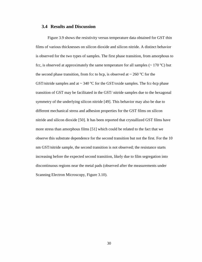
3.4 Results and Discussion
Figure 3.9 shows the resistivity versus temperature data obtained for GST thin
films of various thicknesses on silicon dioxide and silicon nitride. A distinct behavior
is observed for the two types of samples. The first phase transition, from amorphous to
fcc, is observed at approximately the same temperature for all samples (~ 170 oC) but
the second phase transition, from fcc to hcp, is observed at ~ 260 oC for the
GST/nitride samples and at ~ 340 oC for the GST/oxide samples. The fcc-hcp phase
transition of GST may be facilitated in the GST/ nitride samples due to the hexagonal
symmetry of the underlying silicon nitride [49]. This behavior may also be due to
different mechanical stress and adhesion properties for the GST films on silicon
nitride and silicon dioxide [50]. It has been reported that crystallized GST films have
more stress than amorphous films [51] which could be related to the fact that we
observe this substrate dependence for the second transition but not the first. For the 10
nm GST/nitride sample, the second transition is not observed; the resistance starts
increasing before the expected second transition, likely due to film segregation into
discontinuous regions near the metal pads (observed after the measurements under
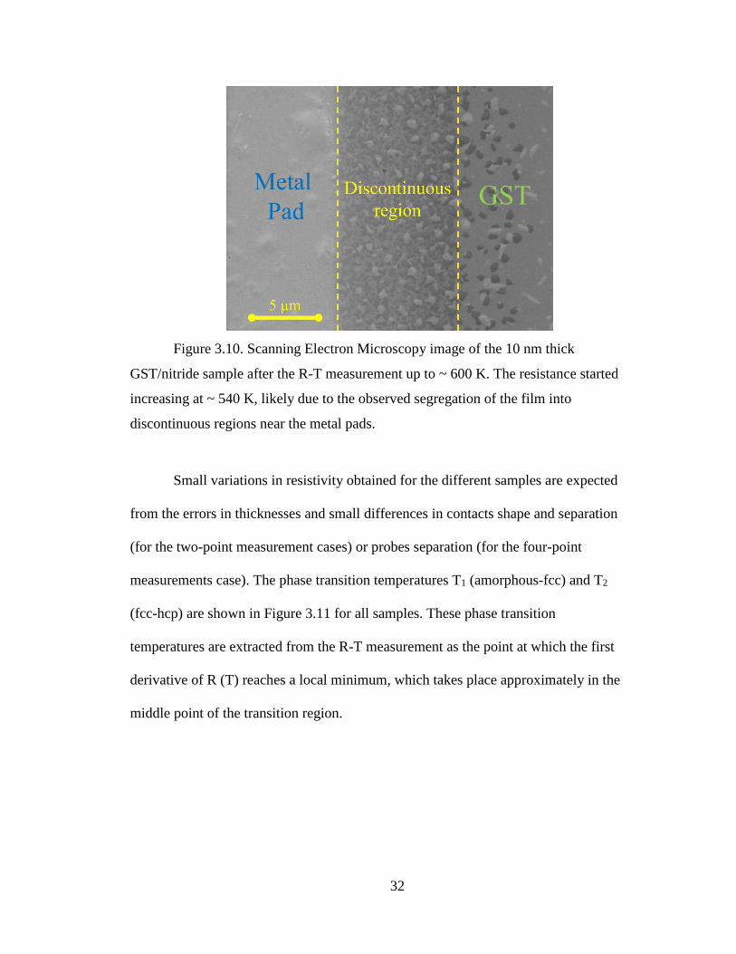
Scanning Electron Microscopy, Figure 3.10).

31
Figure 3.9. Resistivity as a function of temperature for Ge2Sb2Te2 films on silicon
nitride and silicon dioxide starting as amorphous (as-fabricated) showing phase
transitions from amorphous to fcc and from fcc to hcp at T1 and T2 respectively.
Resistivity is extracted from resistance measurements using two-point measurement with
platinum contacts or four-point measurements using tungsten tips directly probing the
GST films. For the thinnest film (10 nm) on silicon nitride the second transition is not
observed as the resistance starts increasing before the expected transition temperature,
possibly due to film segregation into discontinuous regions.
32
Figure 3.10. Scanning Electron Microscopy image of the 10 nm thick
GST/nitride sample after the R-T measurement up to ~ 600 K. The resistance started
increasing at ~ 540 K, likely due to the observed segregation of the film into
discontinuous regions near the metal pads.
Small variations in resistivity obtained for the different samples are expected
from the errors in thicknesses and small differences in contacts shape and separation
(for the two-point measurement cases) or probes separation (for the four-point
measurements case). The phase transition temperatures T1 (amorphous-fcc) and T2
(fcc-hcp) are shown in Figure 3.11 for all samples. These phase transition
temperatures are extracted from the R-T measurement as the point at which the first
derivative of R (T) reaches a local minimum, which takes place approximately in the
middle point of the transition region.

33
Figure 3.11. GST phase transition temperatures T1 (amorphous to fcc) and T2
(fcc to hcp) as a function of film thickness obtained from various measurements on
both GST/oxide (T1 ◊, T2 ) and GST/nitride (T1 T2 Δ ) samples. For the
GST/nitride samples large area contact pads were used for 2-point R-T measurements.
For the GST/oxide samples tungsten probe tips were used for 4-point measurements.
In all 50 nm GST/oxide samples the GST film was patterned by deposition through a
contact mask. One of the 50 nm thick GST/nitride samples () was measured using
tungsten tips to directly probe the GST film (4-point measurement). The 100 nm thick
GST/nitride sample was measured with similar size contacts (~ 1 mm x 1 mm) formed
using graphite paste. The transition temperatures are extracted as the point at which
the first derivative reaches the two local minima.
Figure 3.12 shows the room-temperature resistivity for all samples in the
amorphous, fcc and hcp phases. The amorphous samples were deposited as
amorphous. The fcc and hcp samples were deposited as fcc or hcp (GST/nitride

34
samples) or heated to temperatures above these phase transitions (GST/oxide
samples). All samples have similar resistivities in each phase indicating that the
crystalline structures in the GST/nitride and GST/oxide samples are similar and that
the as-deposited or crystallized fcc and hcp phases are also similar.
The effect of two different heating rates (1 K/min and 5 K/min) on the R-T
characteristics was found to be significant (Figure 3.13). The phase transitions are
observed at slightly lower temperatures for the slower heating rate (for both
GST/nitride and GST/oxide samples). For the GST/nitride samples, the transition
temperatures appear to increase with increasing film thickness, with a more marked
trend for the faster heating rate [52].
Figure 3.12. Room temperature resistivity for all thickness films on
GST/nitride and GST/oxide samples, in amorphous, cubic and hexagonal phases. The
fcc and hcp GST films on GST/oxide sample are obtained by heating as-deposited

35
amorphous films to 565 K or 670 K (above the first or second transition) followed by
cooling to room temperature for resistivity measurements. GST films on GST/nitride
samples are deposited as amorphous, fcc or hcp.
Figure 3.11 shows that, for films from ~ 10 to ~ 100 nm thickness, the first
transition temperature did not depend on the film thickness but the second transition
temperature increased as the film thickness increased. These earlier measurements had
been performed in N2 atmosphere using an inductive heating setup, with an average
heating rate of ~ 3 K/min from room temperature to the maximum temperature of ~
330 oC (no temperature controller) and the sample temperature was measured by a K-
type thermocouple clamped to the sample surface [47]. While there still appears to be
a small thickness dependence effect on the transition temperatures of the GST films on
silicon nitride using a slow heating rate (1 K/min) (Figure 3.13) the current data shows
that the heating rate has a more significant effect on the observed transition
temperatures. This could be due to the difference between the measured chuck
temperature and the actual film temperature; however, the large chuck, samples, and
separation between the probe tips suggest the observed transition temperature
variations with heating rate and thickness (especially for the faster heating rate) are
more likely due to the finite crystallization times of the material at a given
temperature.

36
Figure 3.13. Phase transition temperatures observed from resistance versus
temperature measurements (R-T) with heating rates of 1 K/min and 5 K/min on GST
films of various thicknesses on GST/oxide (left) and GST/nitride (right) samples.
If the crystallization times are slow compared to the heating rate, the structure
does not have time to re-arrange itself before the resistance is measured and the
transition will appear to happen at a higher temperature. For the thicker GST/oxide
samples heated at 5 K/min (50 and 100 nm), the fcc-hcp phase transition is not
observed, presumably because it occurs at a temperature higher than can be reached
with the setup (~ 400 oC) or because it is slow compared to the heating rate.

37
4. The Effect of a Baseline Voltage on Crystallization of Nanoscale
Ge2Sb2Te5 Devices
The crystallization time scale of Ge2Sb2Te5 ranges from > 10 years at room
temperature [53]to ~100 ns close to melting temperature (Tmelt-GST ~900 K) [11, 38, 54-
59] with maximum growth velocity of ~1 m/s [60].
Recent reports of very fast crystallization in pore PCM structures ( < 1ns) upon
melting with a low voltage baseline before and after the melting pulse attribute this
accelerated crystallization to the formation of a pre-nucleated state by the baseline
voltage (after the pulse) [61].
We have combined detailed electrical measurements with finite element
modeling to understand the effect of different baseline voltages on the crystallization of
GST line structures after melting pulses and possible origins for the apparent very fast
crystallization.
4.1 Constant Baseline Voltage Before and After Melting
4.1.1 Experiments on GST Line Cells
A baseline voltage is applied before and after a melting reset pulse to control
and monitor the crystallization dynamics, as shown in Figure 4.1. Experimented GST
line cell structures with bottom metal contacts were fabricated using conventional
photolithography and semiconductor processing techniques on bulk Si wafers.
Detailed fabrication processes described in section 2.2. The resulting device
dimensions were measured by Scanning Electron Microscope (SEM) (Figure 4.3 b).
The baseline electrical measurements were performed by melting the wires via
38
self-heating by applying a short voltage pulse with varying baseline voltage amplitudes
before and after the pulse (Figure 4.1 a). An Agilent 8114A pulse generator (PGU) and a
Tektronix TDS 724D oscilloscope were configured as shown in Figure 4.1 a inset for the
measurements, using short coaxial cables for connections. Several load resistors are used
to limit the current during the pulse to prevent damage of the device breakage. Load
resistors were provided by either mounting them on micro-manipulator probe arms
(leading to additional 10 pf capacitance) or by a surface-mount resistor attached to the
probe tips (Figure 4.1 b inset) (without any additional capacitance). 2 to 3 V pulses with
100 ns durations and varying baseline offset were applied to fully melt GST wires of
varying sizes.
Complete melting of the structures is observed as a plateau in the current during
the pulse (Figure 4.1 b), as observed earlier for silicon microwires [36]. The shapes of the
electrical current versus time characteristics (Figure 4.1 b) suggest that after the melting
pulse, the GST wires may stay partially molten (due to retention of a current carrying
filament) and recrystallize in a growth-from-melt manner, or they may resolidify
immediately as amorphous depending on the applied baseline voltage (Figure 4.2 ). A
liquid filament region has enough heat capacity to crystallize the surrounding solidified
region after the main pulse. The baseline voltage is used to measure the wire resistance
before and after the pulse to determine the phase of the material.
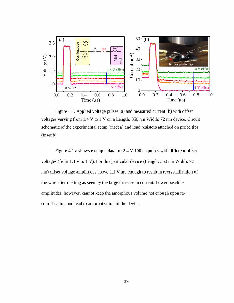
39
Figure 4.1. Applied voltage pulses (a) and measured current (b) with offset
voltages varying from 1.4 V to 1 V on a Length: 350 nm Width: 72 nm device. Circuit
schematic of the experimental setup (inset a) and load resistors attached on probe tips
(inset b).
Figure 4.1 a shows example data for 2.4 V 100 ns pulses with different offset
voltages (from 1.4 V to 1 V). For this particular device (Length: 350 nm Width: 72
nm) offset voltage amplitudes above 1.1 V are enough to result in recrystallization of
the wire after melting as seen by the large increase in current. Lower baseline
amplitudes, however, cannot keep the amorphous volume hot enough upon re-
solidification and lead to amorphization of the device.
0.0 0.2 0.4 0.6 0.8 1.00
10
20
30
40
50
Cu
rren
t (m
A)
Time (s)
1.4 V offset
1 V offset
0.0 0.2 0.4 0.6 0.8 1.0
1.0
1.5
2.0
2.5
L 350 W 72
Volt
age
(V)
Time (s)
1.4 V offset
1 V offset
PG
UOsc
illo
sco
pe
50 Ω
50 Ω
50 Ω GST
1 MΩ
RL
(a) (b)
RL on probe tip

40
Figure 4.2. Measured current signals on a GST wire with varying offset voltages
(1.5 V to 1.2 V) (a), with different offset voltages (b) to show the effect of offset voltage
by switching between amorphous and crystalline phases.
Figure 4.2 shows measured current signals on a GST wire (L: 360 nm W: 62
nm) for 100 ns pulses with varying offset voltages amplitudes. Maximum applied
voltage is kept at 4V for all cases while varying the baseline amplitude. Above 1.2 V
offset voltage, the material re-crystallizes after re-solidification (R wire = 5.7 kΩ) via
liquid filament retention. For 1.2 V offset voltage, the current decreases as the solid
amorphous material cools down and the wire remains amorphous (R wire = 26.6 MΩ).
After the wire is amorphized (R wire = 26.6 MΩ) due to the low offset voltage, a new
pulse is applied with a higher offset amplitude (3V + 1.5 V offset) and the wire
recrystallizes (R wire = 3.3 kΩ). This process is then repeated (3.3 k Ω → 94 MΩ →
3.47 kΩ) to show that the same melting pulse followed by smaller or larger baseline
voltage can be used to repeatedly amorphize or crystallize the structure (Figure 4.2 b).
0 200 400 600 800 10000.0
0.2
0.4
0.6
0.8
1.0
1.2
1.4
Set
Reset
Set
L360 W62
Offset voltage
1.5 V
1.3 V
1.5 V
Cu
rren
t (m
A)
Time (ns)0 200 400 600 800 1000
0.0
0.2
0.4
0.6
0.8
1.0
1.2
Offset voltage
1.5 V
1.4 V
1.3 V
1.2 V
L360 W62
Cu
rren
t (m
A)
Time (ns)
(a) (b)

41
4.1.2 Simulations of GST Line Cells
Unlike conventional electronic devices, PCM utilizes heating to crystallize (set),
and melting and resolidification to amorphize (reset). Hence, the material in the active
region changes dynamically along with the thermal profiles. Many different models have
been proposed to model the changes in the material during operation and the resulting
device behavior. First, compact models have been proposed to construct SPICE models
of PCM devices and optimize cell geometries [62-65]. These compact models however
rely on many assumptions including device symmetry, and do not account for stochastic
nucleation or filament formation. These models also do not calculate local phase
distributions within devices during their operation. To model the phase change properties
of the material, many Arrhenius (JMAK) models have been proposed [66, 67]. These
models use Arrhenius approximations for the crystal fraction as a function of time in
PCM devices. In our laboratory electrothermal models have been used to model both set
and reset operations of PCM devices, including temperature dependent physical
parameters of the materials and thermoelectric effects [16, 32, 68, 69]. In order to capture
the nucleation, growth and amorphization processes during the simulations, these models
have evolved to include a local crystal density function (CD) which is tracked using a
rate equation and where CD = 0 and CD = 1 correspond to fully amorphous and fully
crystalline volumes.[70] This crystal density model includes crystalline nucleation rate
and growth velocity of the material from the literature.
GST line cell structure (Figure 4.3) is simulated using COMSOL Multiphysics
finite element simulations with 2-D rotational geometry. The device dimensions and

42
series load resistor (3kΩ) are chosen to get a similar GST volume with our
experimental GST line cell structures.
Figure 4.3. Schematics of a fabricated line cell structure with contact pads (a). SEM
image of a fabricated line cell (b) Cross section of the simulated line cell geometry and
materials (c).
10 V 100 ns main pulse with varying offset voltages are applied 1µs long to
observe the change of current after the main pulse. The large output currents are indicate
that the GST is molten with main pulse and depend on the offset voltage amplitude, line
cell is crystallized (4.5 V to 2.05 V) or amorphized (under 2 V) (Figure 4.4 a). Figure 4.4
b shows that GST line cell resistances, where low offset voltage applied, increase over
500 Ω
GST
TiN
SiO2
94 nm
70 nm
27
0 n
m
48
0 n
m
600 nm
200 nm
500 Ω 3000
(c)
Silicon Substrate
Oxide
GST
Metal Pad
(a)
500 nm
GST
(b)
500 nm
GST
TiN
TiN(b)

43
time due to fast quenching (amorphous phase). The line cells which are subjected to
higher offset voltage, show lower resistances due to crystallization of the line cells after
main pulse.
Figure 4.4. Output currents (a), and calculated resistances (b) with varying
baseline voltages on simulated (Length 400 nm, Diameter 94 nm) GST line cell. Output
currents (c), and calculated resistances (d) with varying baseline voltages on simulated
(30 nm thick, Diameter 200 nm) GST pore-like structure.
0 2 4 6 8 100
3
6
9
12
15
18200 nm Diameter
Curr
ent
(mA
)
Time (ns)
0.3 V
0.35 V
0.4 V
0.45 V
0 2 4 6 8 1010
1
102
103
104
105
106
107
200 nm Diameter
Res
ista
nce
(
)
Time (ns)
0.3 V
0.35 V
0.4 V
0.45 V
(c) (d)
0.0 0.2 0.4 0.6 0.8 1.00.0
0.5
1.0
1.5
2.0
2.5
3.0
3.5
3 V
3.5 V
4 V
4.5 V
1.5 V
2 V
2.05 V
2.5 V
Offset Voltage
L 400 Dia. 94 nm
Time (s)
Cu
rren
t (m
A)
0.0 0.2 0.4 0.6 0.8 1.010
2
103
104
105
106
107
108
L 400 Dia. 94 nm
Res
ista
nce
(
) Time (s)
3 V
3.5 V
4 V
4.5 V
1.5 V
2 V
2.05 V
2.5 V
Offset Voltage
(a) (b)

44
4.1.3 Simulations of GST Pore-like Cells
Pore-like structure PCM cells with Ge2Sb2Te5 as the phase-change material are
simulated using COMSOL Multiphysics finite element tool with 2D rotational
symmetry, to compare to previously reported experimental results [61]. The GST cells
consist of top and bottom TiN contacts with diameter (d) x height (h) = 250 nm x 200
nm, a GST disk in center (height = 30 nm) with varying diameters (d = 25, 50,100,
and 150 nm) and SiO2 as the surrounding material. This geometry and dimensions
were chosen to match the reported experimental devices [61].
Figure 4.5. Schematic of the simulated pore-like structure PCM cell (a).
Applied voltage as a function of time ( are indicate at the end of the main pulse and
at the end of the simulation) (b). Measured current through the GST cell (c).
TiN
TiN
50 Ω
0 1 2 28 29 300.0
0.3
0.6
0.9
1.2
1.5
Vo
ltag
e (V
)
Time (ns)
0 2 4 6 810
-4
10-3
10-2
10-1
100
101 200 nm Diameter
Cu
rren
t (m
A)
Time (ns)
Offset voltage
0.3 V
0.35 V
0.4 V
0.45 V
(a) (b)
(c)

45
Figure 4.5 a shows the geometry of the simulated GST pore-like cell. PCM
cells simulated by applying 1.3V, 500 ps main pulse with 100 ps rise/fall times on
varying baseline voltages (0.3 V- 0.45 V) for a total simulation period of 30 ns.
The large output currents indicate that the GST is molten with the main pulse
and depending on the offset voltage amplitude, the line cell is crystallized (0.45 V and
0.4 V) or re-solidifies and remains amorphous (under 0.35 V). Figure 4.5 c shows that
with low offset voltages the GST line cell resistance increases over time due to fast
quenching (amorphous phase). With higher offset voltages the line cells show lower
resistances due to crystallization after the main pulse.
Figure 4.6 shows the temperature profiles of the simulated GST structure (200
nm diameter) with 4 different offset voltage amplitude, at the end of the main pulse
and at the end of the simulation (indicated with stars in Figure 4.5 b). White contour
lines denote the regions which have reached melting (>873 K). During the pulse and
due to the cylindrical shape of the structure the current is confined to an outer region
creating a molten ring within the GST. After the pulse, and with large baseline
voltages, the molten region shifts and stabilizes at the center of the device due to the
surrounding SiO2. Low baseline voltages are not sufficient to keep the region molten
and it re-solidifies in amorphous phase.

46
Figure 4.6. Temperature profile of the simulated pore-like structure PCM cell
(200 nm diameter GST) using the four different baseline voltages (Figure 1c). Images
are captured at the end of the main pulse and at the end of the simulation (indicated in
Figure 1b).
The maximum temperature reached as a function of baseline voltage, at the end
of the main pulse, is shown in Figure 4.7 for two different GST thicknesses (30 and 50
nm). Some part of the GST element stays molten with lower baseline voltages (>325
mV) for narrower devices (50,100 nm diameter). Wider structures (200, 300 nm
diameter) require higher baseline voltage amplitude (> 400 mV) to retain a molten
region due to higher volume and heat diffusion, compared to narrower structures.
0.325 V 0.35 V 0.4 V 0.45 V
End of the main pulse (1.6 ns)
End of the simulation (30 ns)
200 nm Diameter
100 nm
TiN
TiN
GST SiO2

47
Figure 4.7. The maximum temperature reached as a function of offset voltage
at the end of the simulation (30 ns).
The simulated current through the 30 nm thick GST structure is shown in
Figure 4.8 for 4 different diameters and 5 different offset voltage amplitudes. The
main pulse partially melts the GST structure (or fully melts it, for the 50 nm diameter
structure) depending on the following applied baseline voltage amplitude; the structure
then re-solidifies as amorphous or recrystallizes (in fcc phase) due to the retained
molten region of GST, again depending on the baseline amplitude which determines
the extent and duration of the retained molten filament. The maximum temperatures
reached within the GST cells as a function of time, for different baseline values are
shown in Figure 4.9. Like for the wider and narrower devices, the longer devices re-
solidify faster than the shorter devices due to faster heat diffusion and larger volumes.
300 350 400 450 500 550200
400
600
800
1000
50 nm High
50 nm
100 nm
200 nm
300 nm
30 nm High
50 nm
100 nm
200 nm
300 nm
Maxim
um
tem
pera
ture
(K
)
Offset Voltage (mV)

48
When the baseline voltage increases the GST element stays at high temperature for a
longer period and the re-solidification process is slower due to the higher current.
Figure 4.8. Simulated current through various diameters GST cells (height of
30 nm) for different baseline voltages.

49
Figure 4.9. Maximum temperature reached within different diameter GST cells
for different baseline voltages as a function of simulation time.
4.2 Decreasing Baseline Voltage after Melting
4.2.1 Experiments on GST Line Cells
GST line cells were annealed at 670 K before the pulse measurements;
therefore all of the cells were initially crystalline (hcp phase). A Tektronix AFG 3102
arbitrary function generator was used to create a 3 step 500 ns long main pulse (3 -
4V), followed by a decreasing multistep offset voltage (1.5 to 1.1 V) for a total 20 ms

50
waveform. A 3kΩ surface-mount resistor was attached to one of the probe tips as a
load resistor to prevent wire breakage caused by high current during the liquid phase.
Applied voltage and output current were captured by a Tektronix DPO 4104
oscilloscope and the wire resistance was obtained from the corresponding data, after
subtraction of the load resistance from the total resistance (Figure 4.10). During the
melting pulse the output current exceeds the oscilloscope acquisition scale settings and
is cropped (Figure 4.10 inset). After the main pulse, the wire becomes molten via self-
heating and due to the large starting applied baseline voltage a liquid filament is
retained. The following decrease in the baseline voltage causes a reduction in the
liquid filament diameter until it completely solidifies. During solidification (~ 1.155
V), the wire resistance suddenly increases (due to the mixed phase upon fast
solidification) before the wire completely crystallizes and the resistance decreases
again. After the measurement, the wire resistance was measured by the PA as 5.711
kΩ indicating the element crystallized into fcc phase.

51
Figure 4.10. Applied voltage and output current (as shown in the measurement
setup in Figure 4.1 a inset), and calculated resistance of the GST line cell (Length 400
Width 140 nm and thickness 50 nm).
4.2.2 Simulations on GST Line Cells
To compare to the experimental results on decreasing baseline voltages after
melting pulses on a GST line cell, COMSOL Multiphysics [71] finite element
simulations of similar waveforms on a GST line with 2-D rotational geometry were
performed (Figure 4.11 a, b) . 2D rotational symmetry is used for practical computational
times. The simulated PCM cell consists of top and bottom TiN contacts with diameter (d)
x height (h) = 150 nm x 500 nm, a GST wire in between of width 50 nm and length 360
nm, and SiO2 as the surrounding isolation material. Cross section schematics of the
simulated wire geometry and materials are shown in Figure 4.11 a including the
simulated 500 Ω series resistor. A 3D sliced view of the simulated line cell is shown
Figure 4.11 b.
hcp
Liquid filament
fccMelting
Solidification
199 200 201 202
1
2
3
4
Volt
age
(V)
Time (s)
L400 W140
0.1
0.2
0.3
0.4
Curr
ent
(mA
)

52
Figure 4.11. Cross section of the simulated line cell geometry and materials. A
resistor is added in series to limit the current (a). 3D sliced view of the simulated cell (b).
A 1.7 V, 50 ns main pulse with a 25 ns rise and 10 ns fall time followed by multi-
step baseline voltages (from 1.30 V to 1.22 V) is applied to GST line cell (Figure 4.12).
The resulting temperature and crystalline density (CD) maps of the simulated cell are
shown in Figure 4.13 with corresponding simulation times. The wire is fully molten by
the short voltage pulse and the current increases due to the decrease of the resistance.
After the main pulse, and during the fall time, a liquid filament is retained, and it starts to
shrink down as the applied baseline voltage decreases until it completely re-solidifies at a
baseline voltage of 1.21V and crystallizes into fcc phase. While the liquid filament
shrinks down it gradually crystallizes the surrounding area due to the high temperature
GST
TiN
SiO2
50 nm
60 nm
24
0 n
m
500 n
m
600 nm
150 nm
500 Ω 500 Ω
(a) (b)

53
and heat capacity of the liquid region. During the solidification of the liquid filament, the
current decreases abruptly due to the significant resistivity difference between the liquid
and crystalline phases. The applied voltage waveform and resulting current and resistance
as a function of simulation time are shown in Figure 4.12.
Figure 4.12 Simulated applied voltage waveform and output current (a) and
resistance and molten volume (b) of the simulated GST line cell (length 360 nm, diameter
50 nm). (c) and (d) show a ‘zoomed-in’ view of the same data in the period after the
melting pulse.
0 1 2 3 4 50
1
2
3
4
5
6L 360 Dia. 50
Res
ista
nce
(k
)
Time (s)
0
1x10⁵
2x10⁵
3x10⁵
4x10⁵
5x10⁵
6x10⁵
7x10⁵
Molt
en a
rea
(nm
3)
(a)
(c)
(b)
(d)
0.0 0.2 0.4 1 2 3 4 5
0.0
0.3
0.6
0.9
1.2
1.5
1.8
Volt
age
(V)
Time (s)
L 360 Dia. 50
0.0
0.4
0.8
1.2
1.6
2.0
Curr
ent
(mA
)
0.0 0.2 0.4 1 2 3 4 50
1
2
3
4
5
6
L 360 Dia. 50
Res
ista
nce
(k
)
Time (s)
0
1x10⁵
2x10⁵
3x10⁵
4x10⁵
5x10⁵
6x10⁵
7x10⁵
Molt
en a
rea
(nm
3)
0 1 2 3 4 5
0.0
0.3
0.6
0.9
1.2
1.5
1.8
Volt
age
(V)
Time (s)
L 360 Dia. 50
0.0
0.4
0.8
1.2
1.6
2.0
Curr
ent
(mA
)

54
Figure 4.13. Temperature and crystalline density profiles of the GST wire during
the simulation, at given simulation times. The white areas indicate the molten regions (T
> 873 K).
The simulations show the same general behavior of the current and resistance of
the cell with decreasing baseline voltages after a melting pulse, in agreement with the
interpretation of the experimental data in terms of a liquid filament that remains after the
melting pulse and leads to crystallization of the surrounding region as it shrinks down.
4.3 Summary
Experiments and simulations show that after a melting pulse, the GST structures
can stay partially molten through the retention of a current carrying filament, re-solidify
as amorphous and crystallize over time, or re-solidify as amorphous and remain
amorphous, depending on the baseline voltage amplitude that follows the melting pulse.
Temperature (K)
Crystalline Density (CD)
72 ns 120 ns 500 ns 2 µs 3.2 µs 3.5 µs 4.5 µs
72 ns 120 ns 500 ns 2 µs 3.2 µs 3.5 µs 4.5 µs

55
These results suggest that in previous reports of ultra-fast crystallization of GST pore-like
cells melted with a ~ 500 ps pulse followed by a baseline voltage, the crystallization
process may have happened after the pulse and because of the baseline voltage that
allowed for re-crystallization [61]. Monitoring the current through the structure is
necessary to understand the phase of the material after the melting pulse.

56
5. In-situ and ex-situ XRD measurements of GeSbTe thin films at
various annealing temperatures
5.1 Introduction
X-ray diffraction measurements were performed on GST thin film samples to
determine the grain sizes with increasing annealing and measurement temperature. Two
types of measurements were conducted, both starting from as-deposited amorphous GST
samples: 1) in-situ annealing with XRD scanning taken during ramping after stabilization
at each target temperature; and 2) annealing at a target temperature (one temperature
ramp from room temperature to final target temperature at which the sample is annealed
for 15 minutes, on a different hot chuck) followed by room temperature XRD
measurements (ex-situ).
5.2 XRD Measurements
The samples used for these experiments were ~ 200 nm thick GST films
deposited on ~ 600 nm SiO2 on single-crystal silicon wafers by co-sputtering
deposition. The GST films were encapsulated with 10 nm Si3N4 to prevent oxidation
and evaporation of the films.
A Bruker D8 Advance x-ray diffraction with nickel coated high vacuum oven
chamber system was used for the in-situ XRD measurements. The system allows
changing the incident beam slits to control the height and width of the incident X-ray
spot. 1 mm and 8 mm slits were used for the X-ray source and detector respectively.
For the in-situ measurements, the samples were annealed from room
temperature to a final temperature in target step temperatures on a hot chuck in the

57
XRD system oven chamber. After the chuck stabilizes at each target temperature the
X-ray scanning was performed with scanning angle (2θ) from 20 to 55 degrees which
takes approximately 34 minutes to complete.
After gathering X-ray intensity data as a function of Bragg angle, background
noise is eliminated by using analysis software. Average grain size is calculated using
the Schrerer equation (Eq. (5.1) ) where L is average grain size [72], K is the
dimensionless shape factor (~0.9-1), λ is the X-ray wavelength and β is the line
broadening at half the maximum intensity (FWHM) in radians.
cos =L
K (5.1)
Figure 5.1 shows an example x-ray intensity peak of GST thin film at 300 oC and
in-situ XRD patterns of GST thin film at various chuck temperatures. The initial GST
thin film is as amorphous and until 175 oC there is no intensity peak. When the chuck
temperature increases, with 2oC/min heating rate, GST starts to crystallize into fcc with
corresponding intensity peaks. The small widening of the intensity peaks as the
temperature increases is caused by an increase in grain size due to temperature dependent
nucleation and growth [73]. When the chuck temperature reaches 300 oC the material
switches from fcc phase to hcp phase. By increasing the chuck temperature to higher

58
temperatures the X-ray peak’s width and maximum intensity continue to increase which
shows increasing crystalline grain sizes up to melting temperature.
Figure 5.1. X-ray intensity peak from GST thin film at 300 oC. The Scherrer
equation is used to calculate average grain size where K is the dimensionless shape factor
(~0.9-1), λ is the X-ray wavelength. Peak width (β) which is Full Width Half Maximum
(FWHM) value inversely proportional to crystallite size (L) (a). In-situ XRD patterns of
200 nm thick GST thin film at various chuck temperature (b).
Figure 5.2. In-situ XRD measurement temperature as a function of time up to 400
oC, in 2 oC/min (a) and 700 oC, in decreasing heating rate (5, 2 and 0.5 oC/min) (b). Flat
temperature regions are ~ 34 minutes and correspond to the XRD scanning time.
28.8 29.2 29.6 30.0
Inte
nsi
ty (
a.u.)
2(deg)
FWHM ()
Cos2
The Scherrer Equation
( )
cos2
L
KB
(a)
23 24 25 26 27 28 29 30
700600
500400
300200
100
2 (deg)
Inte
nsi
ty (
a.u.)
Tem
pera
ture
(o C
)
(b)
0 100 200 300 400 500 6000
50
100
150
200
250
300
350
400 hcpfcc
Tem
per
ature
(oC
)
Time (min)
amp
0 200 400 600 800 10000
100
200
300
400
500
600
700hcpfcc
Tem
per
ature
(oC
)
Time (min)
(a) (b)

59
Figure 5.3 shows average grain sizes calculated from in-situ XRD patterns for
200 nm thin film GST at various chuck temperature, and corresponding resistance
versus temperature characteristics for a different 200 nm thick GST thin film sample
(measured on a different hot chuck setup). Figure 5.2b) shows the same average grain
sizes of 200 nm thin film GST together with nucleation rate and growth velocity of
GST as a function of temperature [73]. After the material starts crystallizing into fcc
nucleation and crystal growth are observed in the XRD results as two distinct
increases in average grain size: first one occurs at the maximum nucleation rate
temperature (~325 oC) and the second one at the maximum growth velocity
temperature (~460 oC). Beyond this temperature there is a continuous but slow
increase in grain sizes due to slow growth velocity (Figure 5.3 b).
Figure 5.3. Average grain sizes (calculated from in-situ XRD data) and
resistances of a different 200 nm thick GST film sample with corresponding phases as a
function of chuck temperature (a). Average grain sizes of 200 nm thin film GST with
nucleation rate and growth velocity [73] of GST as a function of temperature. Grain sizes
are jumping where nucleation rate (also phase change from fcc to hcp) and growth
velocity are maximized.
0 100 200 300 400 500 60010
20
30
40
50
60
70
80
hcpfccAmorphous
Av
erag
e g
rain
siz
e (n
m)
Temperature (oC)
200 nm GST
101
102
103
104
105
106
107
Res
ista
nce
(
)
0 100 200 300 400 500 60010
20
30
40
50
60
70
80
Aver
age
gra
in s
ize
(nm
)
Temperature (oC)
1018
1020
1022
1024
1026
1028
1030
1032
Nucl
eati
on r
ate(
m-3s-1
)
0.0
0.2
0.4
0.6
0.8
1.0
1.2
Gro
wth
Vel
oci
ty (
m/s
)(a) (b)

60
Figure 5.4. Room temperature resistivity and average grain size as a function of
anneal temperature for 100 and 200 nm thickness GST films (a). Average grain sizes of
two 200 nm films calculated from in-situ XRD measurements (squares) and of 100 nm
and 200 nm calculated from (ex-situ) XRD measurements (circle and diamonds) after
pre-annealing at the given temperatures (x-axis) for 15 min (b).
5.3 Finite Element Simulations
Crystallization dynamics of GST cells are analyzed using COMSOL Multiphysics
[71] finite element simulations with planar geometry (Figure 5.5 a) using the
electrothermal and crystal density (CD) models referred to previously [70] which include
GST nucleation rate and growth velocity parameters from the literature.
200 300 400 500 600
10-5
10-4
10-3
100 nm
200 nm
Res
isti
vit
y (
.m)
Anneal temperature (oC)
10
20
30
40
50
60
70
100 nm
200 nm
Av
erag
e g
rain
siz
e (n
m)
200 300 400 500 60010
20
30
40
50
60
70
Av
erag
e g
rain
siz
e (n
m)
Temperature (oC)
in-situ XRD
in-situ XRD
pre-annealed 200 nm
pre-annealed 100 nm
(a) (b)

61
Figure 5.5. Cross section of the planar mushroom cell geometry and materials
simulated using COMSOL multiphysics with the electrothermal and CD models
mentioned earlier [70] (a). GST region of (20 nm depth) planar mushroom cell with
varying crystalline size after 200 ns annealing at 300 oC (b), 350 oC (c), and 400 oC (d).
In these simulations the device is annealed at different constant temperatures from t=0 to
t=200 ns.
The temperature dependent nucleation and growth functions used in the model
lead to different crystalline grain distributions at the different temperatures with larger
grain sizes at higher temperatures as expected (Figure 5.5 b,c,d), with ~20, 25, and 45
nm average grain sizes after 200 ns anneal at 300 oC, 350 oC, and 400 oC, respectively.
The white lines show the grain boundaries that are modeled between the growing
grains. The average grain sizes are obtained from the simulated final grain
distributions using the image processing and particle analysis software ImageJ [74].
In Figure 5.6 the average grain sizes obtained from in-situ XRD measurements
are plotted together with those from the simulated annealed mushroom cell at different
anneal temperatures. The simulated and experimental anneals are quite different and on
time-scales that are orders of magnitude apart (simulated 200 ns at a constant temperature
GST
TiN
25 nm
140 nm
20 nm
100 nm
100 nm
25 nm
SiO2
(a)
300 oC
350 oC
400 oC
(b)
(c)
(d)
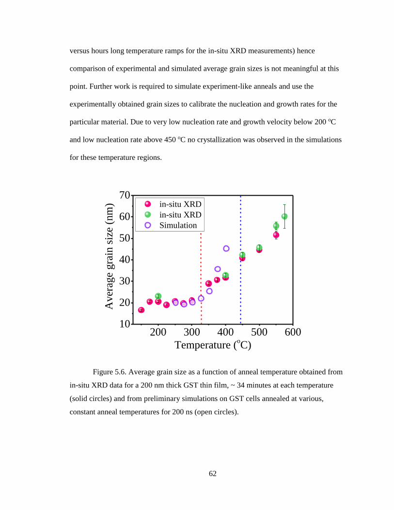
62
versus hours long temperature ramps for the in-situ XRD measurements) hence
comparison of experimental and simulated average grain sizes is not meaningful at this
point. Further work is required to simulate experiment-like anneals and use the
experimentally obtained grain sizes to calibrate the nucleation and growth rates for the
particular material. Due to very low nucleation rate and growth velocity below 200 oC
and low nucleation rate above 450 oC no crystallization was observed in the simulations
for these temperature regions.
Figure 5.6. Average grain size as a function of anneal temperature obtained from
in-situ XRD data for a 200 nm thick GST thin film, ~ 34 minutes at each temperature
(solid circles) and from preliminary simulations on GST cells annealed at various,
constant anneal temperatures for 200 ns (open circles).
200 300 400 500 60010
20
30
40
50
60
70 in-situ XRD
in-situ XRD
Simulation
Av
erag
e g
rain
siz
e (n
m)
Temperature (oC)

63
6. Conclusion
This work focused on temperature dependent characterization of GeSbTe thin
films and nanoscale structures with the goal of contributing to a better understanding of
phase-change memory materials and devices.
Electrical resistivity of liquid GST (ρGST-Lq ) was extracted as 1.26 ± 0.15 mΩ.cm
from thin film measurements and as 0.31 ± 0.04 mΩ.cm and 0.21 ± 0.03 mΩ.cm from 20
nm and 50 nm thick structures from a large number of measurements on individual GST
nanostructures self-heated to melt by single microsecond voltage pulses. Breaking of the
thin film in liquid state suggests that thin film measurements overestimate the liquid
resistivity value. These first results on nanoscale device level measurements of liquid
GST electrical resistivity are in good agreement to those reported for liquid GST
measured by melting bulk GST in a macroscopic setup (~ 0.36 mΩ.cm at ~ 990 K with a
TCR of -0.8 μΩ.cm/K[33]). The difference could be explained by an average temperature
within the liquid GST nanostructures of ~ 1056 K for the 20 nm thick structures and of ~
1170 K for the 50 nm thick structures, which appear to be reasonable (though not
experimentally or computationally confirmable at this point due to lack of experimental
techniques or accurate enough models to estimate the temperature distribution within the
molten GST nanostructures).
We have compared the crystallization behavior of GST films on silicon nitride
and on silicon dioxide through slow resistance versus temperature measurements.
While the first phase transition, from amorphous to fcc, is observed at approximately
the same temperature for all samples (~ 170 oC), the second phase transition, from fcc
to hcp, is observed at ~ 260 oC for the GST/nitride samples and at ~ 340 oC for the

64
GST/oxide samples. Silicon nitride appears to facilitate the fcc-hcp phase-transition of
GST and we speculate this may be due to the hexagonal symmetry of silicon nitride
[49]. Our results also show the importance of the heating rate in determining phase
transition temperatures. Knowledge of the crystallization behavior of GST and how it
is affected by different underlying films is important for design of phase-change
memory devices.
The effect of the baseline voltage on the crystallization behavior of nanoscale
Ge2Sb2Te5 line cells was investigated with experiments and simulations by applying a
voltage pulse (melting pulse) with varying baseline voltages. A baseline (offset) voltage
can play an important role in the set operation (maintaining a molten filament by melting
the amorphous region and utilizing growth-from-melt templated from the crystalline
regions). After the melting pulse, the GST wires stay either partially molten (by retaining
of a current carrying filament) and recrystallize, or they resolidify as amorphous,
depending on the applied baseline. Our electro-thermal models also show the same
current-time characteristics and capture the filament formation and crystallization
dynamics shown in our experiments.
Finally, XRD measurements on as-deposited amorphous GST thin films were
performed in-situ up to high temperatures and ex-situ, at room temperature on pre-
annealed samples at various temperatures, to characterize grain size distributions.
Average grain sizes of GST were calculated from the XRD data using the Scherrer
equation. These results will be used to improve and calibrate our electrothermal and
crystallization models which currently use GST nucleation rate and velocity growth
parameters available in the literature. Preliminary simulations were performed to show

65
example grain distributions obtained in mushroom cells annealed at constant
temperatures. However, given very different heating conditions in the experiments and
simulations, further modeling work is required for a meaningful comparison to the
experimental data, which in turn will enable validation and improvement of the
models. The relative grain orientations and electrical and thermal grain boundaries
resistances may play important roles in the crystallization mechanisms.
The experimental results presented in this thesis are expected to contribute to a
better understanding and more accurate models for phase-change memory materials
and devices.
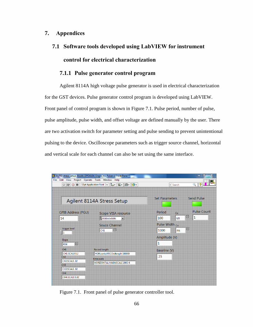
66
7. Appendices
7.1 Software tools developed using LabVIEW for instrument
control for electrical characterization
7.1.1 Pulse generator control program
Agilent 8114A high voltage pulse generator is used in electrical characterization
for the GST devices. Pulse generator control program is developed using LabVIEW.
Front panel of control program is shown in Figure 7.1. Pulse period, number of pulse,
pulse amplitude, pulse width, and offset voltage are defined manually by the user. There
are two activation switch for parameter setting and pulse sending to prevent unintentional
pulsing to the device. Oscilloscope parameters such as trigger source channel, horizontal
and vertical scale for each channel can also be set using the same interface.
Figure 7.1. Front panel of pulse generator controller tool.

67
7.1.2 Oscilloscope data acquisition program
A computer controlled Tektronix DPO4104 oscilloscope is used to capture
applied voltage amplitude and current for electrical characterization. Front panel of
control program is shown in Figure 7.2. Measurements are saved with prefix in file path,
which is the directory name, adding file number and a suffix of ‘.txt’ to the prefix. The
file number is incremented if the counter button is activated by the user. Counter can be
reset with reset button to initialize for the new data file name. Preferred channels can be
defined (voltage, current, or resistance) and selected by turning on and off “active”
buttons for each channel. Resistance is calculated by using voltage and current data.
Waveform chart is included to plot the data during acquisition.
Figure 7.2. Front panel of Tektronix DPO 4104 Oscilloscope data acquisition tool.

68
7.1.3 Cryogenic probe station and temperature controller data
acquisition program
Janis UHT-500 cryogenic probe station and temperature controller are used in
electro-thermal characterization of GST devices. Front panel of Janis UHT-500 cryogenic
probe station and temperature controller data acquisition program is shown in Figure 7.3.
Most of the information such as file names, measurement parameters, and user comments
are saved in an index file. Data file name is defined by the user. Control program has 4
inputs and each input can be chosen as silicon diode, positive temperature coefficient
resistance temperature detector (PTC-RTD), negative temperature coefficient resistance
temperature detector (NTC-RTD), and thermocouple. There are 2 control outputs which
controlled by 3 outputs mode (Closed Loop Proportional Integral Derivative (PID) mode,
Zone mode, and Open Loop mode). Close loop PID mode is chosen in GST device
measurements to control the output which is linked one of the input sensor to give
feedback for stabilization to the target temperature. Control outputs are connected to the
resistive heaters which will be setup with start, stop and step temperature configurations
for the measurement temperatures. Heaters can also be setup with heating rate (high,
medium or low) ramp rate (K/min) defined by user. Temperature or the sensor unit of the
each channel are shown in indicators and plotted in waveform charts. Maximum
threshold temperature for each channel is defined to protect silicon diode sensors which
can be withstand up to 450 K. Resistance value is calculated by using semiconductor
parameter analyzer that controlled with sub VI in main program.

69
Figure 7.3. Front panel of Janis UHT-500 cryogenic probe station and
temperature controller data acquisition tool.
7.1.4 Semiconductor parameter analyzer control program
A computer controlled HP 4145B and Agilent 4156C Parameter analyzers are
used for current voltage (I-V) measurement of the GST devices. Front panel of control
program is shown in Figure 7.4. The parameter analyzer program is modified version of
Ali Gokirmak’s parameter analyzer controller program developed for HP 4145B
parameter analyzers [75]. Most of the information such as file names, measurement
parameters, and user comments are saved in an index file. Measurements are saved with
70
prefix in file path, which is the directory name, adding file number and a suffix of ‘.data’
to the prefix. The file number is incremented if the counter button is activated by the user.
Counter can be reset with reset button to initialize for the new data file name. Parameter
analyzer can be set to make single or multiple measurements by turning on and off the
“single” button. Multiple measurements can be interrupted by “stop” button. There are 4
source measurement units (SMU) which can be set as voltage, current, ground or constant
voltage. The name and plotting function of each SMU can be defined by the user. Control
tool have 2 variable voltage settings and one prime voltage setting for the opposite
voltage sweep. If the hysteresis button is active, after the measurement, the program
changes the parameters for variable 1 to apply a reverse sweep. Measurements can be
setup in different time domains by changing the wait and interval time settings.
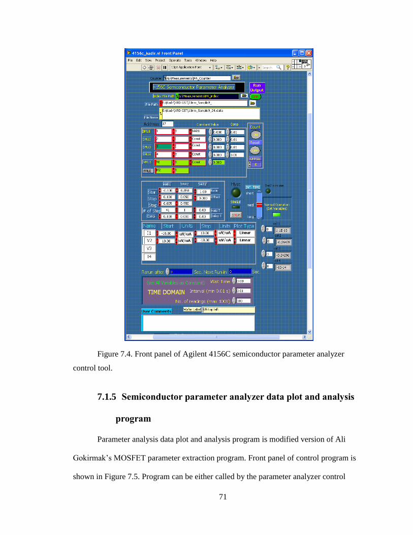
71
Figure 7.4. Front panel of Agilent 4156C semiconductor parameter analyzer
control tool.
7.1.5 Semiconductor parameter analyzer data plot and analysis
program
Parameter analysis data plot and analysis program is modified version of Ali
Gokirmak’s MOSFET parameter extraction program. Front panel of control program is
shown in Figure 7.5. Program can be either called by the parameter analyzer control

72
program or run independently to extract the parameters such as slope, resistance,
intercept and conductance. Most of the information about extraction of the data such as
file names, input values and calculated parameters are saved in a parameter file. Multiple
data sets can be plot on top of each other in the same graph by turning off “clear” button
or using “counter” button with specified starting and ending data number. 4 point
resistance and conductance calculation functions are added for the R-T measurements.
Figure 7.5. Front panel of semiconductor parameter analyzer data plot and
analyzer tool.

73
7.1.6 Function generator unit control program
Tektronix AFG 3102 Dual Channel Arbitrary/Function Generator is used to create
arbitrary voltage pulses for electrical characterization of GST devices. Front panel of the
control program is shown in Figure 7.6. Most of the information such as file names,
measurement parameters and user comments are saved in an index file. Arbitrary signal
created with 4 different sections. Pre-pulse section is created to measure initial device
resistance. Main pulse section will be setup with start, stop and step configurations for the
melting pulse. Post pulse flat section allows device for quenching with defined time and
offset value. Post pulse section will setup to observe crystallization of the device at
higher temperatures. Oscilloscope parameters such as input impedances, trigger setup,
vertical, and horizontal scales can also be set using the same interface. Before applying
the signal, waveform has to be loaded to the function generator by activating “reset
parameters” button. Due to the max length of the waveform (128 K) which function
generator can support, the maximum time scale is defined as 2 ms for the measurements.
Hysteresis button provides AC segments after the pulse with the amplitudes are stepped
up and then down.

74
Figure 7.6. Front panel of Tektronix AFG-3102 function generator control tool.
7.1.7 Oscilloscope data acquisition program
A computer controlled Tektronix DPO4104 oscilloscope is used to capture
applied voltage amplitude and current for electrical characterization. Front panel of
control program is shown in Figure 7.7. Waveform chart is included to plot the data
during acquisition. This is the updated version of the previous data acquisition program
comes with index file, separate wave form chart for each channel, and average offset
calculation. Average offsets can be extracted before the measurement by acquiring

75
constant DC voltage amplitude and calculate average value then subtracted to calibrate
the data. If the data length 10 million data points, data is acquired as 10 equal segments
sequent by using Matlab code integration into LabVIEW due to the large file size.
Figure 7.7. Front panel of Tektronix DPO-4104 oscilloscope data acquisition tool.

76
7.2 Optical band gap measurement for amorphous GST thin film
Optical band gap of 100 nm thin film GST was measured by using Ultraviolet
(UV) - Near Infrared (NIR) Spectrometer. The optical reflection spectrum of GST film
was recorded in the 200-1600 nm wavelength range and the obtained data is shown in
Figure 7.8. The optical reflection spectrum of the 100 nm GST thin film is obtained by
Agilent Cary 5000 UV-VIS-NIR spectrometer with external Agilent DRA-2500 diffuse
reflectance accessory. Reflectance measurements are made by sample on the sphere wall,
ensuring efficient collection of a high proportion of diffusely reflected radiation [76].
0 300 600 900 1200 1500 1800
60
80
100
120
140
160
Ref
lect
ance
(R
%)
Wavelength (nm)
100 nm amorphous GST
Figure 7.8. Optical reflection spectrum of the 100 nm amorphous GST thin film in
200-1600 nm wavelength range.
The most common models to determine the optical band gap of semiconductors is
Tauc model (7.1) which allows us to derive the band gap energy from absorption
coefficient and photon energy as a function of incident energy [77]. Energy band gap (Eg)
in terms of absorption coefficient α is given by;
)( gEhAh (7.1)

77
where A is constant hv is photon energy and α is absorption coefficient which can
be written in terms of reflectance as (7.2);
)]R-(R)/ R-[(Rln =t2 minminmax (7.2)
where t is the thickness of the film and R is reflectance. Sudden fall in reflectance
from Rmax to Rmin is observed due to the absorption of light by the material. The usual
method to calculate energy band gap is to plot graph between (αℎν) 1/2 and ℎν where the
intercept of the abscissa indicates the optical band gap.
Figure 7.9 shows reflectance as a function of photon energy for 100 nm GST thin
film. In Figure 7.10 the intercept of the abscissa indicates 1.16 eV as optical band gap of
the 100 nm amorphous GST thin film.
1.0 1.5 2.0 2.5 3.0 3.5
0
20
40
60
80
[hl
n(R
max
-Rm
in)/
(R-R
min)
]2
Energy Band Gap (h)
100 nm amorphous GST
Figure 7.9. Plotting based on the relationship of [hν ln (Rmax-Rmin)/(R-Rmin)] 2
and hν for 100 nm amorphous GST thin film. The intercept in the abscissa indicates an
optical band gap of 1.16 eV (inset).

78
0.96 1.04 1.12 1.200
20
40
60
80
[hl
n(R
max
-Rm
in)/
(R-R
min)
]2
Energy Band Gap (h)
100 nm amorphous GST
1.16 eV
Figure 7.10. Fitting based on the relationship of [hν ln (Rmax-Rmin)/(R-Rmin)] 2
and hν for 100 nm amorphous GST thin film. 1.16 eV is determined as optical band gap
of the amorphous GST film.
7.3 Scanning Auger Microscope Setup
The AES system uses a cylindrical mirror analyzer (CMA). Electron beam (2.0
keV Kinetic Energy 10.0 keV) originates at CeB6 (or LaB6) ceramic filament. The
beam is focused onto a specimen and emitted electrons are deflected around the electron
gun and pass through an aperture towards the back of the CMA. Electron beam travels
along central axis of energy analyzer, passing through the electron condenser
(controlling sample beam current) and objectives lenses (for focusing beam) and finally
the octapole deflector (for beam rastering, imaging). After hitting the sample,
backscattered and Auger electrons that have the right trajectory pass through the entrance
grid and hit the Secondary Electron Detector (SED), where the produced signal is used
for imaging the surface. After electrons pass through the entrance grid, they enter the

79
space between the coaxial cylinders. A negative potential is applied to the outer cylinder,
and a smaller negative potential may be applied to the inner cylinder. If the electron
kinetic energy varies only slightly from the right value, the electron will pass through the
exit grid, pass through an aperture and hit the electron multiplier detector. If the electron
energy deviates too much from the right value, it will get lost in the energy analyzer and
be absorbed into a metal part (e.g., the inner cylinder). By varying the potentials on the
two cylinders (the potentials on the outer and inner cylinders are ramped), the energies of
the electrons that can be detected are changed and it allows derivative mode plotting of
the Auger data. An optional ion gun can be integrated for depth profiling experiments
(Figure 7.11).
Figure 7.11. Auger depth profiling schematics.
e- e-e-
Ar+ ion milling
e-beam
gun
e-

80
Figure 7.12. SEM images of the pulsed GST device (Width: 96 nm and Length:
220 nm). 100 x 100 µm contact pads are shown in top figure. Higher magnification SEM
images shows the metal contact (middle figure) and GST device (bottom figure).
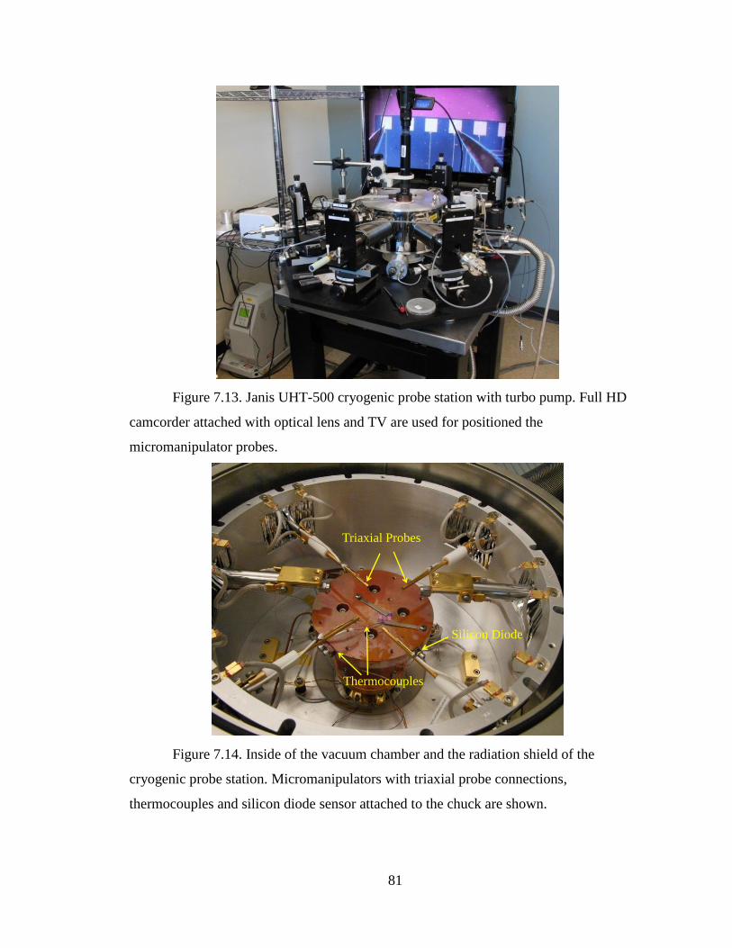
81
Figure 7.13. Janis UHT-500 cryogenic probe station with turbo pump. Full HD
camcorder attached with optical lens and TV are used for positioned the
micromanipulator probes.
Figure 7.14. Inside of the vacuum chamber and the radiation shield of the
cryogenic probe station. Micromanipulators with triaxial probe connections,
thermocouples and silicon diode sensor attached to the chuck are shown.
Silicon Diode
Thermocouples
Triaxial Probes
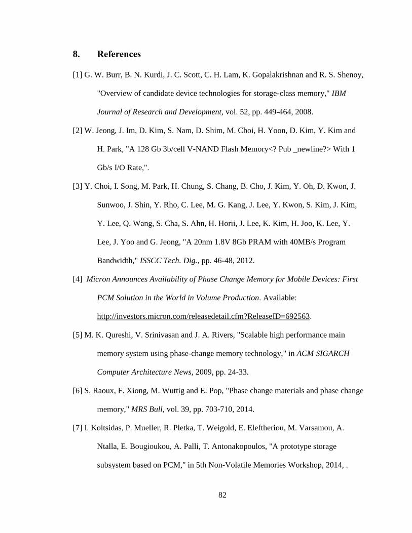
82
8. References
[1] G. W. Burr, B. N. Kurdi, J. C. Scott, C. H. Lam, K. Gopalakrishnan and R. S. Shenoy,
"Overview of candidate device technologies for storage-class memory," IBM
Journal of Research and Development, vol. 52, pp. 449-464, 2008.
[2] W. Jeong, J. Im, D. Kim, S. Nam, D. Shim, M. Choi, H. Yoon, D. Kim, Y. Kim and
H. Park, "A 128 Gb 3b/cell V-NAND Flash Memory<? Pub _newline?> With 1
Gb/s I/O Rate,".
[3] Y. Choi, I. Song, M. Park, H. Chung, S. Chang, B. Cho, J. Kim, Y. Oh, D. Kwon, J.
Sunwoo, J. Shin, Y. Rho, C. Lee, M. G. Kang, J. Lee, Y. Kwon, S. Kim, J. Kim,
Y. Lee, Q. Wang, S. Cha, S. Ahn, H. Horii, J. Lee, K. Kim, H. Joo, K. Lee, Y.
Lee, J. Yoo and G. Jeong, "A 20nm 1.8V 8Gb PRAM with 40MB/s Program
Bandwidth," ISSCC Tech. Dig., pp. 46-48, 2012.
[4] Micron Announces Availability of Phase Change Memory for Mobile Devices: First
PCM Solution in the World in Volume Production. Available:
http://investors.micron.com/releasedetail.cfm?ReleaseID=692563.
[5] M. K. Qureshi, V. Srinivasan and J. A. Rivers, "Scalable high performance main
memory system using phase-change memory technology," in ACM SIGARCH
Computer Architecture News, 2009, pp. 24-33.
[6] S. Raoux, F. Xiong, M. Wuttig and E. Pop, "Phase change materials and phase change
memory," MRS Bull, vol. 39, pp. 703-710, 2014.
[7] I. Koltsidas, P. Mueller, R. Pletka, T. Weigold, E. Eleftheriou, M. Varsamou, A.
Ntalla, E. Bougioukou, A. Palli, T. Antonakopoulos, "A prototype storage
subsystem based on PCM," in 5th Non-Volatile Memories Workshop, 2014, .

83
[8] T. Nirschl, J. B. Phipp, T. D. Happ, G. W. Burr, B. Rajendran, M. -. Lee, A. Schrott,
M. Yang, M. Breitwisch, C. -. Chen, E. Joseph, M. Lamorey, R. Cheek, S. -.
Chen, S. Zaidi, S. Raoux, Y. C. Chen, Y. Zhu, R. Bergmann, H. -. Lung and C.
Lam, "Write strategies for 2 and 4-bit multi-level phase-change memory," in
Electron Devices Meeting, 2007. IEDM 2007. IEEE International, 2007, pp. 461-
464.
[9] M. Stanisavljevic, A. Athmanathan, N. Papandreou, H. Pozidis and E. Eleftheriou,
"Phase-change memory: Feasibility of reliable multilevel-cell storage and
retention at elevated temperatures," in Reliability Physics Symposium (IRPS),
2015 IEEE International, 2015, pp. 5B. 6.1-5B. 6.6.
[10] B. C. Lee, E. Ipek, O. Mutlu and D. Burger, "Architecting phase change memory as
a scalable dram alternative," ACM SIGARCH Computer Architecture News, vol.
37, pp. 2-13, 2009.
[11] H. -. P. Wong, S. Raoux, S. B. Kim, J. Liang, J. P. Reifenberg, B. Rajendran, M.
Asheghi and K. E. Goodson, "Phase Change Memory," Proc. IEEE, vol. 98, pp.
2201-2227, 2010.
[12] S. Raoux and M. Wuttig, "Phase change materials: Science and applications," in
Phase Change Materials: Science and Applications, S. Raoux, Ed. Springer
Verlag, 2008, pp. 99-116.
[13] L. v. Pieterson, Phase Change Materials: Science and Applications, S. Raoux and
M. Wuttig, Eds. Springer Verlag, 2008, pp. 86.
[14] K. Cil, F. Dirisaglik, L. Adnane, M. Wennberg, A. King, A. Faraclas, M. B.
Akbulut, Y. Zhu, C. Lam and A. Gokirmak, "Electrical Resistivity of

84
Liquid Ge2Sb2Te5 Based on Thin-Film and Nanoscale Device Measurements,"
IEEE Trans. Electron Devices, vol. 60, pp. 433-437, 2013.
[15] A. Faraclas, G. Bakan, L. Adnane, F. Dirisaglik, N. Williams, A. Gokirmak and H.
Silva, "Modeling of Thermoelectric Effects in Phase Change Memory Cells,"
Electron Devices, IEEE Transactions on, vol. 61, pp. 372-378, 2014.
[16] F. Dirisaglik, G. Bakan, A. Faraclas, A. Gokirmak and H. Silva, "Numerical
Modeling of Thermoelectric Thomson Effect in Phase Change Memory Bridge
Structures," Int. J. Hi. Spe. Ele. Syst., vol. 23, pp. 1450004, 03/01; 2014/05, 2014.
[17] U. Gottlieb, X. Sun, E. Kolawa and M. Nicolet, "Temperature dependence of
resistivity for TiN and ti-si-N films," in Materials Research Society Symposium
Proceedings, 1996, pp. 361-364.
[18] J. F. Shackelford and W. Alexander, CRC Materials Science and Engineering
Handbook. CRC, 2001.
[19] Y. Yin, H. Sone and S. Hosaka, "Finite element analysis of dependence of
programming characteristics of phase-change memory on material properties of
chalcogenides," Japanese Journal of Applied Physics, vol. 45, pp. 8600, 2006.
[20] Y. Liu, Z. Song, Y. Ling, Y. Gong and S. Feng, "Three-dimensional numerical
simulation of phase-change memory cell with probe like bottom electrode
structure," Japanese Journal of Applied Physics, vol. 48, pp. 024502, 2009.
[21] J. P. Reifenberg, K. W. Chang, M. A. Panzer, S. Kim, J. A. Rowlette, M. Asheghi,
H. S. P. Wong and K. E. Goodson, "Thermal boundary resistance measurements
for phase-change memory devices," Electron Device Letters, IEEE, vol. 31, pp.
56-58, 2010.

85
[22] J. Lee, M. Asheghi and K. E. Goodson, "Impact of thermoelectric phenomena on
phase-change memory performance metrics and scaling," Nanotechnology, vol.
23, pp. 205201, 2012.
[23] A. Faraclas, N. Williams, F. Dirisaglik, K. Cil, A. Gokirmak and H. Silva,
"Operation dynamics in phase-change memory cells and the role of access
devices," in VLSI (ISVLSI), 2012 IEEE Computer Society Annual Symposium on,
2012, pp. 78-83.
[24] A. Faraclas, N. Williams, G. Bakan, A. Gokirmak and H. Silva, "Comparison of
instantaneous crystallization and metastable models in phase change memory
cells," in Device Research Conference (DRC), 2012 70th Annual, 2012, pp. 145-
146.
[25] D. H. Kim, F. Merget, M. Först and H. Kurz, "Three-dimensional simulation model
of switching dynamics in phase change random access memory cells," J. Appl.
Phys., vol. 101, pp. 064512, 2007.
[26] L. Crespi, A. Ghetti, M. Boniardi and A. L. Lacaita, "Electrical Conductivity
Discontinuity at Melt in Phase Change Memory," IEEE Electron Device Letters,
vol. 35, pp. 747-749, 2014.
[27] R. Fallica, J. L. Battaglia, S. Cocco, C. Monguzzi, A. Teren, C. Wiemer, E. Varesi,
R. Cecchini, A. Gotti and M. Fanciulli, "Thermal and Electrical Characterization
of Materials for Phase-Change Memory Cells†," Journal of Chemical &
Engineering Data, vol. 54, pp. 1698-1701, 2009.

86
[28] H. K. Lyeo, D. G. Cahill, B. S. Lee, J. R. Abelson, M. H. Kwon, K. B. Kim, S. G.
Bishop and B. Cheong, "Thermal conductivity of phase-change material
GeSbTe," Appl. Phys. Lett., vol. 89, pp. 151904, 2006.
[29] Yizhang Yang, Hendrik F. Hamann, Mehdi Asheghi*, "- Thermal Conductivity
Measurements and Modeling of Phase-Change Ge2Sb2Te5 Materials," -
Nanoscale and Microscale Thermophysical Engineering, vol. 13, pp. - 88, 2009.
[30] L. Adnane, N. Williams, H. Silva and A. Gokirmak, "High temperature setup for
measurements of Seebeck coefficient and electrical resistivity of thin films using
inductive heating," Rev. Sci. Instrum., vol. 86, pp. 105119, 2015.
[31] F. Yan, T. Zhu, X. Zhao and S. Dong, "Microstructures and thermoelectric
properties of GeSbTe based layered compounds," Appl. Phys. A, vol. 88, pp. 425-
428, 2007.
[32] N. Kan'an, A. Faraclas, N. Williams, H. Silva and A. Gokirmak, "Computational
analysis of rupture-oxide phase-change memory cells," Electron Devices, IEEE
Transactions on, vol. 60, pp. 1649-1655, 2013.
[33] R. Endo, S. Maeda, Y. Jinnai, R. Lan, M. Kuwahara, Y. Kobayashi and M. Susa,
"Electric Resistivity Measurements of Sb2Te3 and Ge2Sb2Te5 Melts Using Four-
Terminal Method," Japanese Journal of Applied Physics, vol. 49, pp. 5802, 2010.
[34] T. Kato and K. Tanaka, "Electronic Properties of Amorphous and Crystalline Ge~
2Sb~ 2Te~ 5 Films," Japanese Journal of Applied Physics Part 1 Regular Papers
Short Notes and Review Papers, vol. 44, pp. 7340, 2005.
[35] www.janis.com. ST-500-UHT Micromanipulated Probe Stations
.

87
[36] G. Bakan, A. Cywar, H. Silva and A. Gokirmak, "Melting and crystallization of
nanocrystalline silicon microwires through rapid self-heating," Appl. Phys. Lett.,
vol. 94, pp. 251910, 2009.
[37] A. Gokirmak, H. Inaltekin and S. Tiwari, "Attofarad resolution capacitance–voltage
measurement of nanometer scale field effect transistors utilizing ambient noise "
Nanotechnology, vol. 20, pp. 335203, 2009.
[38] D. Lencer, M. Salinga and M. Wuttig, "Design Rules for Phase‐Change Materials in
Data Storage Applications," Adv. Mater., vol. 23, pp. 2030-2058, 2011.
[39] H. Kobatake, H. Fukuyama, I. Minato, T. Tsukada and S. Awaji, "Noncontact
measurement of thermal conductivity of liquid silicon in a static magnetic field,"
Appl. Phys. Lett., vol. 90, pp. 094102, 2007.
[40] A. Cywar, J. Li, C. Lam and H. Silva, "The impact of heater-recess and load
matching in phase change memory mushroom cells," Nanotechnology, vol. 23,
pp. 225201, 2012.
[41] S. Raoux and M. Wuttig, "Phase change materials: Science and applications," in ,
Paul Fons, Ed. Springer, 2008, pp. 155.
[42] Y. Choi, M. Jung and Y. Lee, "Effect of Heating Rate on the Activation Energy for
Crystallization of Amorphous Ge2Sb2Te5 Thin Film," Electrochemical and
Solid-State Letters, vol. 12, pp. F17-F19, 2009.
[43] N. Ohshima, "Crystallization of germanium–antimony–tellurium amorphous thin
film sandwiched between various dielectric protective films," J. Appl. Phys., vol.
79, pp. 8357-8363, 1996.

88
[44] S. Raoux, G. Burr, M. Breitwisch, C. Rettner, Y. Chen, R. Shelby, M. Salinga, D.
Krebs, S. Chen and H. Lung, "Phase-change random access memory: A scalable
technology," IBM Journal of Research and Development, vol. 52, pp. 465-479,
2008.
[45] S. Raoux, J. L. Jordan-Sweet and A. J. Kellock, "Crystallization properties of
ultrathin phase change films," J. Appl. Phys., vol. 103, pp. 114310-114310-7,
2008.
[46] Y. Yin, H. Sone and S. Hosaka, "Dependences of electrical properties of thin
GeSbTe and AgInSbTe films on annealing," Jpn. J. Appl. Phys, vol. 44, pp. 6208,
2005.
[47] H. Peng, K. Cil, A. Gokirmak, G. Bakan, Y. Zhu, C. Lai, C. Lam and H. Silva,
"Thickness dependence of the amorphous-cubic and cubic-hexagonal phase
transition temperatures of GeSbTe thin films on silicon nitride," Thin Solid Films,
vol. 520, pp. 2976-2978, 2012.
[48] D. K. Schroder, Semiconductor Material and Device Characterization. Wiley Online
Library, 2006.
[49] C. Wang, X. Pan, M. Rühle, F. Riley and M. Mitomo, "Silicon nitride crystal
structure and observations of lattice defects," J. Mater. Sci., vol. 31, pp. 5281-
5298, 1996.
[50] C. Deng, Y. Geng, Y. Wu, Y. Wang and J. Wei, "Adhesion effect of interface layers
on pattern fabrication with GeSbTe as laser thermal lithography film,"
Microelectronic Engineering, vol. 103, pp. 7-11, 2013.

89
[51] I. Park, J. Jung, S. Ryu, K. Choi, B. Yu, Y. Park, S. M. Han and Y. Joo,
"Thermomechanical properties and mechanical stresses of Ge< sub> 2</sub> Sb<
sub> 2</sub> Te< sub> 5</sub> films in phase-change random access memory,"
Thin Solid Films, vol. 517, pp. 848-852, 2008.
[52] K. Cil, Y. Zhu, J. Li, C. H. Lam and H. Silva, "Assisted cubic to hexagonal phase
transition in GeSbTe thin films on silicon nitride," Thin Solid Films, vol. 536, pp.
216-219, 6/1, 2013.
[53] F. Dirisaglik, G. Bakan, Z. Jurado, S. Muneer, M. Akbulut, J. Rarey, L. Sullivan, M.
Wennberg, A. King and L. Zhang, "High speed, high temperature electrical
characterization of phase change materials: metastable phases, crystallization
dynamics, and resistance drift," Nanoscale, vol. 7, pp. 16625-16630, 2015.
[54] S. Raoux, M. Wuttig and L. v. Pieterson, Phase Change Materials: Science and
Applications. Springer Verlag, 2008.
[55] M. Wuttig and N. Yamada, "Phase-change materials for rewriteable data storage,"
Nature Materials, vol. 6, pp. 824-832, 2007.
[56] D. Ielmini and A. L. Lacaita, "Phase change materials in non-volatile storage,"
Materials Today, vol. 14, pp. 600-607, 2011.
[57] A. Lacaita, "Phase change memories: State-of-the-art, challenges and perspectives,"
Solid-State Electronics, vol. 50, pp. 24-31, 2006.
[58] J. Hegedüs and S. Elliott, "Microscopic origin of the fast crystallization ability of
Ge–Sb–Te phase-change memory materials," Nature Materials, vol. 7, pp. 399-
405, 2008.

90
[59] B. Lee, G. W. Burr, R. M. Shelby, S. Raoux, C. T. Rettner, S. N. Bogle, K.
Darmawikarta, S. G. Bishop and J. R. Abelson, "Observation of the role of
subcritical nuclei in crystallization of a glassy solid," Science, vol. 326, pp. 980-
984, 2009.
[60] G. W. Burr, P. Tchoulfian, T. Topuria, C. Nyffeler, K. Virwani, A. Padilla, R. M.
Shelby, M. Eskandari, B. Jackson and B. Lee, "Observation and modeling of
polycrystalline grain formation in Ge2Sb2Te5," J. Appl. Phys., vol. 111, pp.
104308-104308-12, 2012.
[61] D. Loke, T. Lee, W. Wang, L. Shi, R. Zhao, Y. Yeo, T. Chong and S. Elliott,
"Breaking the speed limits of phase-change memory," Science, vol. 336, pp.
1566-1569, 2012.
[62] K. Sonoda, A. Sakai, M. Moniwa, K. Ishikawa, O. Tsuchiya and Y. Inoue, "Compact
modeling of phase-change memories," in Simulation of Semiconductor Processes
and Devices 2007Anonymous Springer, 2007, pp. 137-140.
[63] I. Chen and E. Pop, "Compact thermal model for vertical nanowire phase-change
memory cells," Electron Devices, IEEE Transactions on, vol. 56, pp. 1523-1528,
2009.
[64] Y. Chen, K. C. Kwong, X. Lin, Z. Song and M. Chan, "3-D Resistance Model for
Phase-Change Memory Cell," 2014.
[65] D. Ventrice, P. Fantini, A. Redaelli, A. Pirovano, A. Benvenuti and F. Pellizzer, "A
phase change memory compact model for multilevel applications," Electron
Device Letters, IEEE, vol. 28, pp. 973-975, 2007.

91
[66] N. Ciocchini and D. Ielmini, "Modeling of crystallization kinetics in phase change
memories for set and read disturb regimes," in Reliability Physics Symposium,
2014 IEEE International, 2014, pp. 5E. 1.1-5E. 1.6.
[67] S. Senkader and C. Wright, "Models for phase-change of GeSbTe in optical and
electrical memory devices," J. Appl. Phys., vol. 95, pp. 504, 2004.
[68] A. Faraclas, N. Williams, A. Gokirmak and H. Silva, "Modeling of Set and Reset
Operations of Phase-Change Memory Cells," Electron Device Letters, IEEE, vol.
32, pp. 1737-1739-3, 2011.
[69] A. Faraclas, G. Bakan, N. Williams, A. Gokirmak and H. Silva, "Modeling of
Thermoelectric Effects in Phase Change Memory Cells," Transactions on
Electron Devices, 2013.
[70] W. Z and G. A. Modeling of phase change memory devices using a dynamic crystal
density approach. Mat. Res. Soc. Spring 2014 Meeting (HH 2.08), 2014.
[71] Available: http://www.comsol.com/.
[72] K. Ishikawa, K. Yoshikawa and N. Okada, "Size effect on the ferroelectric phase
transition in PbTiO 3 ultrafine particles," Physical Review B, vol. 37, pp. 5852,
1988.
[73] G. W. Burr, P. Tchoulfian, T. Topuria, C. Nyffeler, K. Virwani, A. Padilla, R. M.
Shelby, M. Eskandari, B. Jackson and B. Lee, "Observation and modeling of
polycrystalline grain formation in Ge2Sb2Te5," J. Appl. Phys., vol. 111, pp.
104308, 2012.
[74] C. A. Schneider, W. S. Rasband and K. W. Eliceiri, "NIH Image to ImageJ: 25 years
of image analysis," Nature Methods, vol. 9, pp. 671-675, 2012.

92
[75] A. G. Gokirmak, Ultra Narrow Silicon FETs Integrated with Microfluidic System for
Serial Sequencing of Biomolecules Based on Local Charge Sensing, 2006.
[76] Available: https://www.agilent.com/cs/library/flyers/Public/5991-
1717EN_PromoFlyer_UV_DRA.pdf.
[77] M. E. Sánchez-Vergara, J. C. Alonso-Huitron, A. Rodriguez-Gómez and J. N.
Reider-Burstin, "Determination of the optical GAP in thin films of amorphous
dilithium phthalocyanine using the Tauc and Cody models," Molecules, vol. 17,
pp. 10000-10013, 2012.