Embed Size (px)
Citation preview
IEEE TRANSACTIONS ON ELECTRON DEVICES, VOL. 47, NO. 4, APRIL 2000 883
Temperature Dependent Minority Electron Mobilitiesin Strained Si1 x
Gex (0:2 0:4) LayersJae-Sung Rieh, Member, IEEE, Pallab K. Bhattacharya, Fellow, IEEE, and Edward T. Croke
Abstract—Temperature-dependent minority electron mo-bilities in p-type SiGe have been measured for the first time.Measurements were made on test npn SiGe/Si heterojunctionbipolar transistors (HBT’s) with pseudomorphic p-type Si1 Ge(0 2 0 4) base layers. Magnetotransport measurementswere performed on the fabricated HBT’s to obtain the minorityelectron mobilities in the heavily B-doped base layers for temper-atures ranging from 5 to 300 K. The measured minority electronmobilities exhibited sharp increase with decreasing temperature,and also showed enhancement with decreasing base Ge com-position. The cut-off frequency technique was also employed toestimate the room temperature minority electron mobilities of thealloys and the results confirmed the trend in mobilities with Gecomposition as determined by the magnetotransport technique.
Index Terms—Heterojunction bipolar transistor, minority car-rier mobility, SiGe alloy.
I. INTRODUCTION
B IPOLAR semiconductor devices are minority carrier de-vices and the device performance is critically affected by
the minority carrier transport characteristics. Among the mi-nority transport parameters, minority carrier mobility may bethe most important one as it dictates the operating speed of thedevices, which is crucial for most of modern device applica-tions. In the past, the minority carrier mobility has been as-sumed equal to the majority carrier mobility for simplicity indevice modeling. However, results reported on carrier transportcharacteristics in Si consistently show that the minority carriermobility is higher than the majority carrier mobility. The differ-ence is particularly significant for heavily doped semiconduc-tors, where the ratio of the two mobilities reaches as high as2–3 at room temperature [1], and it gets even larger as tempera-ture is lowered [2], [3]. The discrepancy is believed to originatefrom the difference in ionized impurity scattering rate, whereelectrostatic repulsion to minority carriers results in less scat-tering than the attraction to majority carriers [4]. As is the case,reliable data on minority carrier mobility values are essential forthe accurate modeling of bipolar semiconductor devices.
Recently, npn SiGe/Si heterojunction bipolar transistors(HBT’s) are receiving considerable attention due to theirsuperior frequency response characteristics compared to those
Manuscript received June 17, 1999; revised October 18, 1999. This work wassupported by NASA-Glenn under Grant NAG3-1903 and by the Jet PropulsionLaboratory under Contract 961358. The review of this paper was arranged byEditor J. N. Hollenhorst.
J.-S. Rieh and P. K. Bhattacharya are with the Department of ElectricalEngineering and Computer Science, University of Michigan, Ann Arbor, MI48109-2122 USA (e-mail: [email protected]).
E. T. Croke is with HRL Laboratories, Malibu, CA 90265 USA.Publisher Item Identifier S 0018-9383(00)02735-0.
of Si bipolar junction transistors (BJT’s). As the base transittime, which limits the frequency response of the devices inmost cases, is determined by the minority electron mobility inthe base region, the information on this parameter in heavilydoped p-type strained SiGe layers is critical for the analysisand optimization of npn SiGe/Si HBT performance. There havebeen several theoretical calculations reported on the minorityelectron mobility in p-type strained Si Ge alloys [5], [6].However, the results were limited to low Ge compositions
and mainly focused on room temperature mobility,except for the calculation by Kayet al. which was made alsoat K [5]. Furthermore, experimental data on minorityelectron mobility in SiGe alloys have not been reported, mainlydue to the difficulty in the measurement of this parameter.Mobilities measured in undoped bulk SiGe alloys in 1960[7] have been the only experimental data available till dateand these values have been referred to as a comparison totheoretical values by many authors. This paper presents thefirst experimental data on minority electron mobilities in p-typestrained Si Ge alloys. The mobilities were measured fortemperatures ranging from 5 to 300 K and for Ge compositionsfrom up to .
Several experimental techniques have been suggested for theextraction of the minority carrier mobilities, many of them in-volving optical excitation of the semiconductors [2], [3], [8].Optical excitation may be useful for bulk material, but it isnot an effective method as far as strained layers are concerned,which is generally too thin to be selectively excited. Instead,techniques that make use of bipolar transistor operations arewidely used for the measurement of the mobility in thin strainedlayers. Among these methods, the magnetotransport technique[9], [10] and cut-off frequency technique [11], [12] are the mostpopular ones. In this study, npn SiGe/Si HBT’s have been fabri-cated with molecular beam epitaxy (MBE) grown heterostruc-tures, and two separate techniques have been employed to mea-sure the minority electron mobilities in the p-type strained SiGebase layers of the fabricated devices. First, the magnetotrans-port technique was used to measure the temperature-dependentmobilities of the alloys. Next, the cut-off frequency techniquewas used to estimate the room temperature mobilities to ensurethe results obtained by the former technique.
II. FABRICATION OF NPN SiGe/Si HBT’s
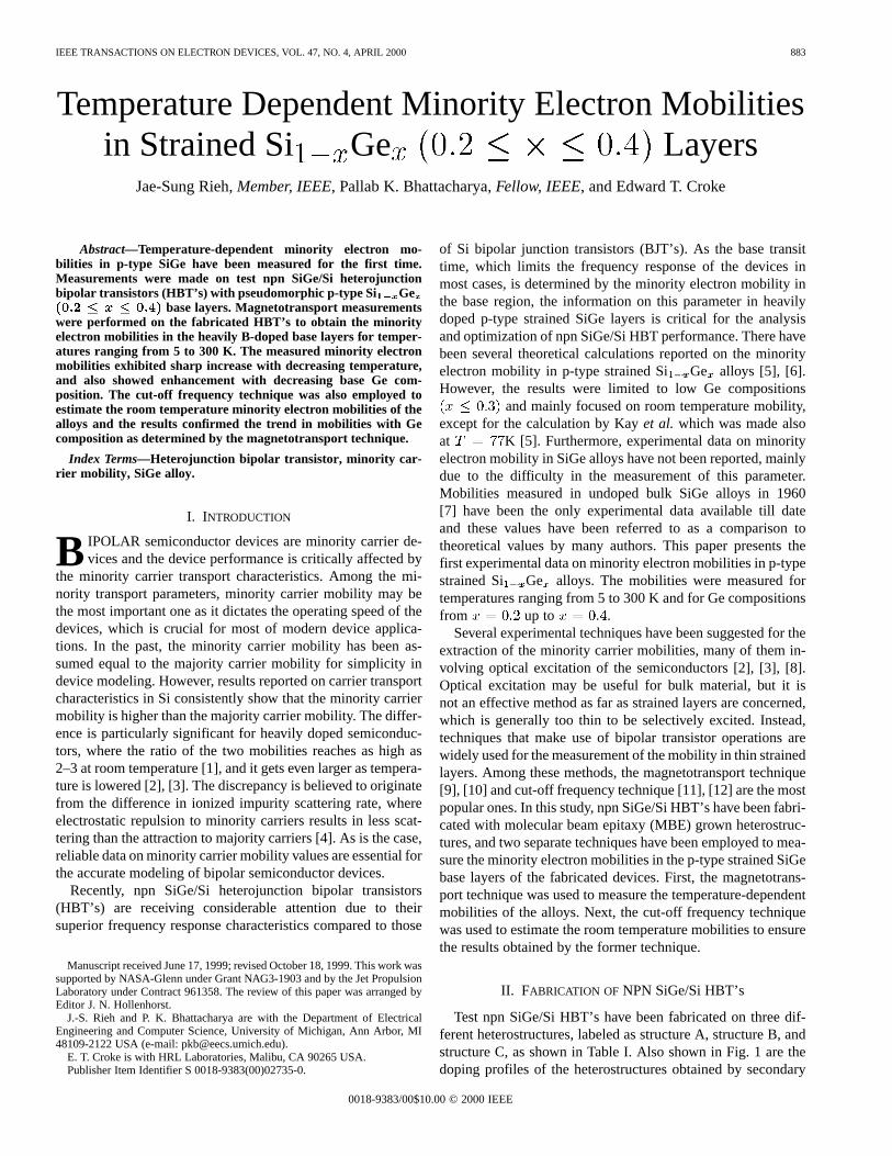
Test npn SiGe/Si HBT’s have been fabricated on three dif-ferent heterostructures, labeled as structure A, structure B, andstructure C, as shown in Table I. Also shown in Fig. 1 are thedoping profiles of the heterostructures obtained by secondary
0018-9383/00$10.00 © 2000 IEEE
884 IEEE TRANSACTIONS ON ELECTRON DEVICES, VOL. 47, NO. 4, APRIL 2000
TABLE IHETEROSTRUCTURE OFTEST npn SiGe/Si
HBT’s GROWN BY MBE. THE Ge COMPOSITIONx = 0:2, 0.3,AND 0.4,AND
THE BASE WIDTH W = 400, 300,AND 200 ÅFORSTRUCTURESA, B, AND C,RESPECTIVELY. NOTE THAT ALL THE NUMBERSGIVEN ARE DESIGNVALUES
Fig. 1. Doping profiles of the test npn Si Ge /Si HBT’s (0:2 � x � 0:4)obtained by SIMS.
ion mass spectrometry (SIMS). The structures are identical ex-cept for the Si Ge base layer where three different Ge com-positions ( , 0.3, and 0.4 for structures A, B, and C, re-spectively) have been employed to investigate the effect of Gecomposition on the mobility. The corresponding base widthswere 400, 300, and 200 Å, respectively, being limited by thecritical thickness. Note that these widths are the design valuesand the actual widths should be somewhat different as will bediscussed later. Doping concentration in the base layers, fromSIMS profile, was cm , except for structure A,which showed slightly higher concentration ofcm . Corresponding doping concentrations from spreading re-sistance analysis (SRA) were cm andcm , respectively. No intentional grading of Ge compositionor doping concentration has been attempted in order to elimi-nate the effect of quasielectric field in the base region. Undopedspacer layers ( Å) are inserted on both sides of the baselayer to suppress the boron outdiffusion from the base. For allthe structures, the epitaxial layers were grown by MBE on topof the As-doped n Si subcollector layer, which was depositedby chemical vapor deposition ( ) on high-resistivity (100)Si substrate. The Sb-doped n-Si collector layer and the B-doped
p strained SiGe base layer were grown at C, whilethe Sb-doped n/n Si emitter layer was grown at a lower temper-ature of C, all at a background pressure oftorr. Owing to the low growth temperature, no indication of dis-locations in the strained SiGe base layer was found. The growthrate was Å/s for the collector and the emitter layers andÅ/s for the base layer.
Double mesa structure HBT’s have been fabricated withstandard lift-off and etching techniques. The emitter contacts(Cr/Au 500/2000 Å) were first evaporated on the highlydoped emitter contact layer, followed by a reactive ion etching(RIE) and KOH-based selective wet etching to expose thebase layer for base metal contacts. The etching selectivity ofthe KOH-based solution (KOH : KCr O : H O 50 g : 2g : 200 ml) between the Si emitter layer and the SiGe baselayer, which is important to prevent the overetch of the thinbase layer, was higher than 10 at a solution temperature of 30C. Vertical emitter side wall profile was obtained by aligning
emitter contact patterns, which was used as an etch mask, along(100) orientation instead of conventional (110) orientation[13]. Self-aligned base contacts (Pt/Au 200/1300 Å) werethen evaporated, followed by RIE down to the subcollectorlayer. Evaporation of collector contacts (Ti/Au500/2000 Å),device isolation by RIE, and the deposition of SiOdielectriclayer by plasma-enhanced CVD (PECVD) were performed insequence. Finally, via hole formation by RIE and the evapo-ration of probing pads (Ti/Al/Ti/Au = 500/11 000/500/3000Å) completed the device fabrication. All the metal contactswere subject to rapid thermal annealing (RTA) to minimize thecontact resistance. The annealing condition was 20 s at 400Cfor the emitter contacts and 3 s at 375C for the base and thecollector contacts. dc and rf characterization of the fabricateddevices were made prior to the mobility measurements. As anexample of device performances, a device from structure C withan emitter size of m exhibited differential cur-rent gain of , and cut-off frequency and maximumoscillation frequency of 30 and 50 GHz, respectively.
III. M OBILITY MEASUREMENT BY MAGNETOTRANSPORT
TECHNIQUE
A. Magnetotransport Technique
Magnetic field provides many useful characterization toolsfor the investigation of carrier transport characteristics in semi-conductors. Hall measurement and geometrical magnetoresis-tance measurement are well-proven and powerful techniques toevaluate the majority carrier mobilities. Recently, Betseret al.have proposed a technique to measure the minority carrier mo-bilities by modifying the geometrical magnetoresistance mea-surement [9]. In this technique, a BJT is biased in common-basemode and operated under an applied magnetic fieldwith fixedemitter current and collector-base voltage , and the mi-nority electron mobility is extracted from the change in basecurrent with varied magnetic field . In the present work,the device was biased in common-emitter mode with fixedand , and the mobility values were extracted by monitoringthe change in with varying magnetic field , being freefrom the assumptions made by Betseret al.such as sufficiently
RIEH et al.: TEMPERATURE DEPENDENT MINORITY ELECTRON MOBILITIES 885
high current gain and negligible backward carrier injection atemitter–base junction. The minority carrier mobility can be re-lated to the fractional change in the collector current andthe applied magnetic field as
(1)
where is the magnetotransport mobility. Therefore, minoritycarrier mobility in the base region can be extracted by plottingthe fractional change in the collector current againstthe magnetic field squared, . It should be noted that the ex-tracted magnetotransport mobility is different from the driftcarrier mobility . The ratio between the two parameters can beassumed equal to the ratio between the geometrical magnetore-sistance mobility and the drift carrier mobility as,
(2)
where is the momentum relaxation time of the carrierswith a kinetic energy of [9]. The ratio is usually close to unityand the details about this parameter will be discussed later.
B. Mobility Measurement by Magnetotransport Technique
Fabricated npn SiGe/Si HBT’s with emitter area ofm have been used for the temperature-dependent mi-
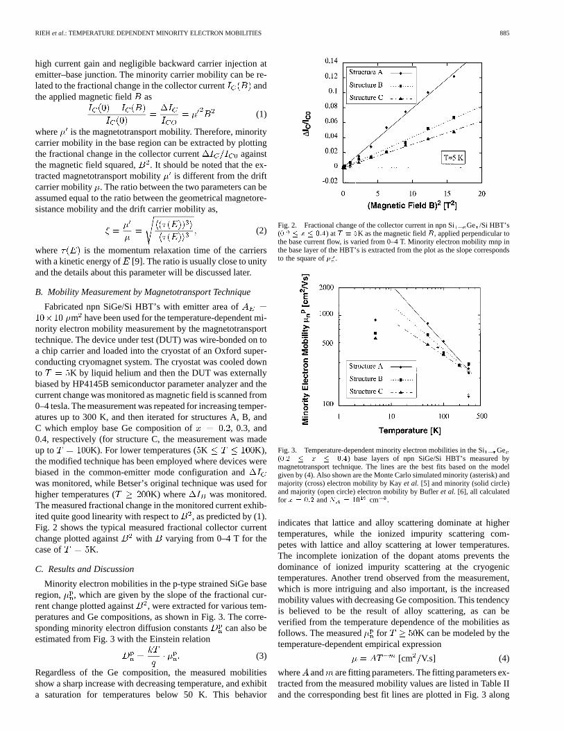
nority electron mobility measurement by the magnetotransporttechnique. The device under test (DUT) was wire-bonded on toa chip carrier and loaded into the cryostat of an Oxford super-conducting cryomagnet system. The cryostat was cooled downto K by liquid helium and then the DUT was externallybiased by HP4145B semiconductor parameter analyzer and thecurrent change was monitored as magnetic field is scanned from0–4 tesla. The measurement was repeated for increasing temper-atures up to 300 K, and then iterated for structures A, B, andC which employ base Ge composition of , 0.3, and0.4, respectively (for structure C, the measurement was madeup to K). For lower temperatures (K K),the modified technique has been employed where devices werebiased in the common-emitter mode configuration andwas monitored, while Betser’s original technique was used forhigher temperatures ( K) where was monitored.The measured fractional change in the monitored current exhib-ited quite good linearity with respect to , as predicted by (1).Fig. 2 shows the typical measured fractional collector currentchange plotted against with varying from 0–4 T for thecase of K.
C. Results and Discussion
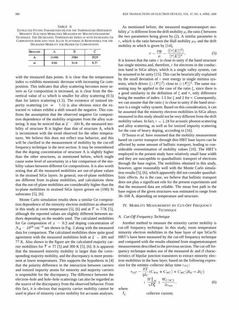
Minority electron mobilities in the p-type strained SiGe baseregion, , which are given by the slope of the fractional cur-rent change plotted against , were extracted for various tem-peratures and Ge compositions, as shown in Fig. 3. The corre-sponding minority electron diffusion constants can also beestimated from Fig. 3 with the Einstein relation
(3)
Regardless of the Ge composition, the measured mobilitiesshow a sharp increase with decreasing temperature, and exhibita saturation for temperatures below 50 K. This behavior
Fig. 2. Fractional change of the collector current in npn SiGe /Si HBT’s(0:2 � x � 0:4) atT = 5K as the magnetic fieldB, applied perpendicular tothe base current flow, is varied from 0–4 T. Minority electron mobility mnp inthe base layer of the HBT’s is extracted from the plot as the slope correspondsto the square of� .
Fig. 3. Temperature-dependent minority electron mobilities in the SiGe(0:2 � x � 0:4) base layers of npn SiGe/Si HBT’s measured bymagnetotransport technique. The lines are the best fits based on the modelgiven by (4). Also shown are the Monte Carlo simulated minority (asterisk) andmajority (cross) electron mobility by Kayet al. [5] and minority (solid circle)and majority (open circle) electron mobility by Bufleret al. [6], all calculatedfor x = 0:2 andN = 10 cm .
indicates that lattice and alloy scattering dominate at highertemperatures, while the ionized impurity scattering com-petes with lattice and alloy scattering at lower temperatures.The incomplete ionization of the dopant atoms prevents thedominance of ionized impurity scattering at the cryogenictemperatures. Another trend observed from the measurement,which is more intriguing and also important, is the increasedmobility values with decreasing Ge composition. This tendencyis believed to be the result of alloy scattering, as can beverified from the temperature dependence of the mobilities asfollows. The measured for K can be modeled by thetemperature-dependent empirical expression
[cm V.s] (4)
where and are fitting parameters. The fitting parameters ex-tracted from the measured mobility values are listed in Table IIand the corresponding best fit lines are plotted in Fig. 3 along
886 IEEE TRANSACTIONS ON ELECTRON DEVICES, VOL. 47, NO. 4, APRIL 2000
TABLE IIEXTRACTED FITTING PARAMETERS (4) FOR THETEMPERATURE-DEPENDENT
MINORITY ELECTRON MOBILITIES MEASURED BY MAGNETOTRANSPORT
TECHNIQUE. THE DECREASINGTEMPERATUREINDEXm WITH INCREASINGGeCOMPOSITIONINDICATES THAT ALLOY SCATTERING IS RESPONSIBLE FOR THE
DEGRADED MOBILITY FOR HIGHER Ge COMPOSITIONS
with the measured data points. It is clear that the temperatureindex exhibits monotonic decrease with increasing Ge com-position. This indicates that alloy scattering becomes more se-vere as Ge composition is increased, as is clear from the the-oretical value of which is smaller for alloy scattering (0.5)than for lattice scattering (1.5). The existence of ionized im-purity scattering ( ) is also obvious since the ex-tracted values exhibit a shift toward the negative. This con-firms the assumption that the observed negative Ge composi-tion dependence of the mobility originates from the alloy scat-tering. It may be noticed that at K, the measured mo-bility of structure B is higher than that of structure A, whichis inconsistent with the trend observed for the other tempera-tures. We believe this does not reflect true behavior, and thiswill be clarified in the measurement of mobility by the cut-offfrequency technique in the next section. It may be rememberedthat the doping concentration of structure A is slightly higherthan the other structures, as mentioned before, which mightcause some level of uncertainty in a fair comparison of the mo-bility values between different Ge compositions. It is also worthnoting that all the measured mobilities are out-of-plane valuesin the strained SiGe layers. In general, out-of-plane mobilitiesare different from in-plane mobilities, and calculations showthat the out-of-plane mobilities are considerably higher than thein-plane mobilities in strained SiGe layers grown on (100) Sisubstrates [5], [6].
Monte Carlo simulation results show a similar Ge composi-tion dependence of the minority electron mobilities as observedin this study at room temperature [5], [6] and at K [5],although the reported values are slightly different between au-thors depending on the models used. The calculated mobilitiesfor Ge composition of and doping concentration of
cm are shown in Fig. 3 along with the measureddata for comparison. The calculated mobilities show quite goodagreement with the measured mobilities both at and77 K. Also shown in the figure are the calculated majority car-rier mobilities for [5] and 300 K [5], [6]. It is apparentthat the measured minority mobility is larger than the corre-sponding majority mobility, and the discrepancy is more promi-nent at lower temperatures. This supports the hypothesis in [4]that the polarity difference in the interaction between carriersand ionized impurity atoms for minority and majority carriersis responsible for the discrepancy. The difference between theelectron–hole and hole–hole scatterings can also be regarded asthe source of the discrepancy from the observed behavior. Fromthis fact, it is obvious that majority carrier mobility cannot beused in place of minority carrier mobility for accurate analyses.
As mentioned before, the measured magnetotransport mo-bility is different from the drift mobility , the ratio betweenthe two parameters being given by (2). A similar parameter is, which is the ratio between the Hall mobility and the drift
mobility m which is given by [14],
(5)
It is known that the ratio is close to unity if the band structurehas single minima and, therefore,for electrons in the conduc-tion band in SiGe alloys, which is a single valley system, canbe assumed to be unity [15]. This can be heuristically explainedby the small deviation of over energy in single minima sys-tems, which drives close to . The same rea-soning may be applied to the case of the ratio, since there isa good similarity in the definition of and , only differencebeing the number of index: 1.5 forand 2 for . Consequently,we can assume that the ratiois close to unity if the band struc-ture is a single valley system. Based on this consideration, it canbe assumed that the minority electron mobilities in SiGe alloysmeasured in this study should not be very different from the driftmobility values. In fact, for acoustic phonon scatteringand alloy scattering, as well as for ionized impurity scatteringfor the case of heavy doping, according to [16].
D’Souzaet al.have reasoned that the mobility measurementbased on carrier transport through thin HBT base layers can beaffected by some amount of ballistic transport, leading to con-siderable overestimation of mobility values [10]. The HBT’semployed in the present study have relatively small base widthand they are susceptible to quasiballistic transport of electronsthrough the base region. The mobilities obtained in this study,however, agree reasonably well with the Monte Carlo simula-tion results [5], [6], which apparently did not consider quasibal-listic effects. As is the case, we believe that ballistic transportdoes not play a significant role for the present experiments andthat the measured data are reliable. The mean free path in thebase region of the given structures was estimated to range from36–168 Å, depending on temperature and structure.
IV. M OBILITY MEASUREMENT BY CUT-OFF FREQUENCY
TECHNIQUE
A. Cut-Off Frequency Technique
Another method to measure the minority carrier mobility iscut-off frequency technique. In this study, room temperatureminority electron mobilities in the base layer of npn SiGe/SiHBT’s have been measured by the cut-off frequency techniqueand compared with the results obtained from magnetotransportmeasurements described in the previous section. The cut-off fre-quency technique makes use of the measured dc and rf charac-teristics of bipolar junction transistors to extract minority elec-tron mobilities in the base layer, based on the following expres-sion for the emitter–collector delay time :
(6)
wherecollector current;
RIEH et al.: TEMPERATURE DEPENDENT MINORITY ELECTRON MOBILITIES 887
and base-emitter and base-collector junction ca-pacitance;
and emitter and collector resistance;and neutral base width and base-collector junction
space charge layer width, respectively;field factor;electron saturation velocity.is the minority electron diffusion constant inthe p-type base region and can be expressedin terms of minority electron mobility bythe Einstein relation given in (3).
It is clear that if the term ( , base transit time)is isolated from (6) by evaluating the other terms, we can extractminority electron mobility from the values of and . Thefirst term on the right hand side (RHS) in (6) can be eliminatedby plotting as a function of reciprocal collector currentand taking the -axis interception point by extrapolation. Theintercept value, , is the emitter–collector delay time withinfinite collector current and equal to the summation of the re-maining three terms on the RHS in the equation. The secondterm on the RHS, the time delay in the collector, can bedetermined by evaluating , , and values from DCand rf measurement of the device. The last term on the RHS,collector space charge layer delay time , is calculatedfrom the values of and obtained from SIMS profileand depletion width calculation. Following this procedure, thevalue of the base transit time can be extracted and the mobility
can be determined.
B. Mobility Estimation by Cut-Off Frequency Technique
Several SiGe/Si HBT’s with typical performance were se-lected from each of the three structures with different Ge com-positions for the measurements. Two different device sizes, withemitter area of m and m , havebeen employed in order to acquire more reliable mobility values.
-parameters of these devices were measured up toGHz with a HP8510C network analyzer for several different col-lector current levels at a fixed collector emitter voltageV. The cut-off frequency, , at each measurement point wasobtained from the frequency response of current gain, and thenconverted to values according the following relation:
(7)
The emitter–collector delay time extracted from the threestructures are plotted against in Fig. 4. As shown in thefigure, is proportional to reciprocal collector current ,except for the large current region where sharp increase in thedelay time is observed due to the Kirk effect. The-axis in-terception point, , is thus determined by extrapolating thelinear fitting line to -axis, and, consequently, the first term onthe RHS in (6) vanishes. The values of averaged over themeasured devices are shown in Table III.
The second term on the RHS in (6) includes base–collectorjunction capacitance and emitter and collector resistance
and , respectively, all of which can be determined fromdc and rf measuremens on the device. One method to evaluate
is to measure the -parameters of the device. The mea-sured -parameters are first converted to-parameters, then
Fig. 4. Measured emitter–collector delay time� of npn Si Ge /SiHBT’s (0:2 � x � 0:4), plotted as a function of reciprocal collector current.Symbols represent the measured data and the lines represent the linear fitting.� is given by the interception point of the plot.
Fig. 5. Measured-fIm[(1 + H )=H ]g of npn Si Ge /Si HBT’s(0:2 � x � 0:4), plotted as a function of frequency. Symbols represent themeasured data and the lines represent the linear fitting. The base–collectorjunction capacitanceC can be extracted from the plot as the slopecorresponds to2�C .
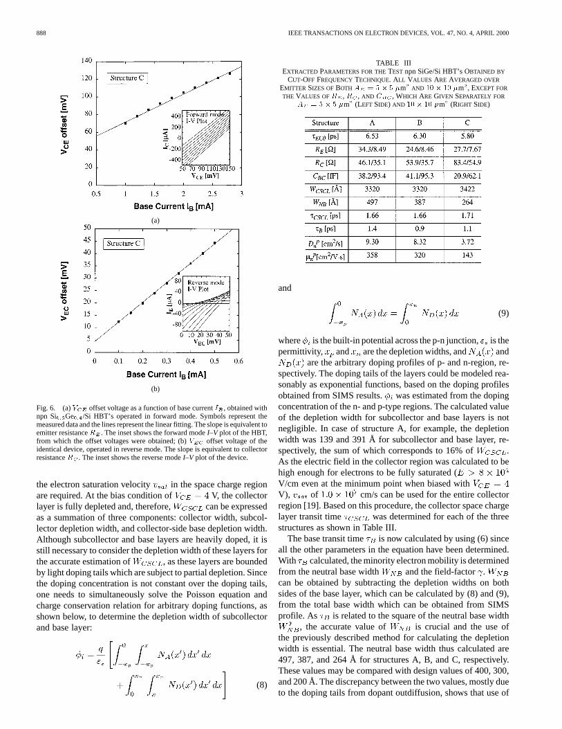
the function- is plotted against fre-quency. The plot generally shows good linearity, as shown inFig. 5 for typical devices from the three structures, and canbe determined from the plot as its slope corresponds toof the device [17]. can be extracted from the base currentdependence of offset voltages in the common emitter cur-rent–voltage (I–V) characteristics of the device. The offsetvoltage increases linearly with increasing base currentandits slope is equivalent to [18]. is extracted in a similarway by operating the device in reverse mode, instead of forwardmode, by exchanging emitter and collector electrodes. The mea-sured offset voltages of a typical device are shown in Fig. 6 forboth forward and reverse mode operation. The insets show theI–Vcharacteristics around the origin, from which the offset volt-ages are extracted. The average values of , , and ex-tracted by these methods are listed in Table III for both emittersizes of m and m .
To determine the last term on the RHS in (6), the values ofbase–collector junction space charge layer width and
888 IEEE TRANSACTIONS ON ELECTRON DEVICES, VOL. 47, NO. 4, APRIL 2000
(a)
(b)
Fig. 6. (a)V offset voltage as a function of base currentI , obtained withnpn Si Ge /Si HBT’s operated in forward mode. Symbols represent themeasured data and the lines represent the linear fitting. The slope is equivalent toemitter resistanceR . The inset shows the forward modeI–V plot of the HBT,from which the offset voltages were obtained; (b)V offset voltage of theidentical device, operated in reverse mode. The slope is equivalent to collectorresistanceR . The inset shows the reverse modeI–V plot of the device.
the electron saturation velocity in the space charge regionare required. At the bias condition of V, the collectorlayer is fully depleted and, therefore, can be expressedas a summation of three components: collector width, subcol-lector depletion width, and collector-side base depletion width.Although subcollector and base layers are heavily doped, it isstill necessary to consider the depletion width of these layers forthe accurate estimation of , as these layers are boundedby light doping tails which are subject to partial depletion. Sincethe doping concentration is not constant over the doping tails,one needs to simultaneously solve the Poisson equation andcharge conservation relation for arbitrary doping functions, asshown below, to determine the depletion width of subcollectorand base layer:
(8)
TABLE IIIEXTRACTED PARAMETERS FOR THETEST npn SiGe/Si HBT’s OBTAINED BY
CUT-OFF FREQUENCYTECHNIQUE. ALL VALUES ARE AVERAGED OVER
EMITTER SIZES OFBOTHA = 5� 5 �m AND 10� 10 �m , EXCEPT FOR
THE VALUES OFR , R , AND C , WHICH ARE GIVEN SEPARATELY FOR
A = 5� 5 �m (LEFT SIDE) AND 10� 10 �m (RIGHT SIDE)
and
(9)
where is the built-in potential across the p-n junction,is thepermittivity, and are the depletion widths, and and
are the arbitrary doping profiles of p- and n-region, re-spectively. The doping tails of the layers could be modeled rea-sonably as exponential functions, based on the doping profilesobtained from SIMS results. was estimated from the dopingconcentration of the n- and p-type regions. The calculated valueof the depletion width for subcollector and base layers is notnegligible. In case of structure A, for example, the depletionwidth was 139 and 391 Å for subcollector and base layer, re-spectively, the sum of which corresponds to 16% of .As the electric field in the collector region was calculated to behigh enough for electrons to be fully saturated (V/cm even at the minimum point when biased withV), of cm/s can be used for the entire collectorregion [19]. Based on this procedure, the collector space chargelayer transit time was determined for each of the threestructures as shown in Table III.
The base transit time is now calculated by using (6) sinceall the other parameters in the equation have been determined.With calculated, the minority electron mobility is determinedfrom the neutral base width and the field-factor .can be obtained by subtracting the depletion widths on bothsides of the base layer, which can be calculated by (8) and (9),from the total base width which can be obtained from SIMSprofile. As is related to the square of the neutral base width
, the accurate value of is crucial and the use ofthe previously described method for calculating the depletionwidth is essential. The neutral base width thus calculated are497, 387, and 264 Å for structures A, B, and C, respectively.These values may be compared with design values of 400, 300,and 200 Å. The discrepancy between the two values, mostly dueto the doping tails from dopant outdiffusion, shows that use of
RIEH et al.: TEMPERATURE DEPENDENT MINORITY ELECTRON MOBILITIES 889
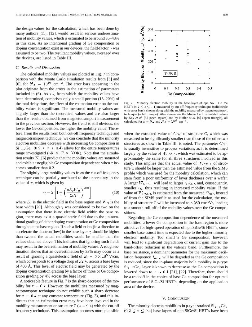
the design values for the calculation, which has been done bymany authors [11], [12], would result in serious underestima-tion of mobility values, which is estimated to be around 35–43%in this case. As no intentional grading of Ge composition ordoping concentration exist in our devices, the field-factorwasassumed to be two. The resultant mobility values, averaged overthe devices, are listed in Table III.
C. Results and Discussion
The calculated mobility values are plotted in Fig. 7 in com-parison with the Monte Carlo simulation results from [5] and[6], for cm . The error bars appearing in theplot originate from the errors in the estimation of parametersincluded in (6). As , from which the mobility values havebeen determined, comprises only a small portion (15–20%) ofthe total delay time, the effect of the estimation error on the mo-bility values is significant. The measured mobility values areslightly larger than the theoretical values and are also largerthan the results obtained from magnetotransport measurementin the previous section. However, the trend is still obvious: thelower the Ge composition, the higher the mobility value. There-fore, from the results from both cut-off frequency technique andmagnetotransport technique, we can conclude that the minorityelectron mobilities decrease with increasing Ge composition inSi Ge ( ) alloys for the entire temperaturesrange investigated (K K). Note that the simula-tion results [5], [6] predict that the mobility values are saturatedand exhibit a negligible Ge composition dependence whenbe-comes smaller than 0.2.
The slightly large mobility values from the cut-off frequencytechnique can be partially attributed to the uncertainty in thevalue of , which is given by
(10)
where is the electric field in the base region and is thebase width [20]. Although was considered to be two on theassumption that there is no electric field within the base re-gion, there may exist a quasielectric field due to the uninten-tional grading of either doping concentration or Ge compositionthroughout the base region. If such a field exists (in a direction toaccelerate the electron flow) in the base layer,should be higherthan twoand the actual mobilities would be smaller than thevalues obtained above. This indicates that ignoring such fieldsmay result in the overestimation of mobility values. A rough es-timation shows that an overestimation by 33% may occur as aresult of ignoring a quasielectric field of V/cm,which corresponds to a voltage drop of across a base layerof 400 Å. This level of electric field may be generated by thedoping concentration grading by a factor of three or Ge compo-sition grading by 4% across the base layer.
A noticeable feature in Fig. 7 is the sharp decrease of the mo-bility for . However, the mobilities measured by mag-netotransport technique do not exhibit such a sharp decreasefor at any constant temperature (Fig. 3), and this in-dicates that an estimation error may have been involved in themobility measurement on structure C ( ) with the cut-offfrequency technique. This assumption becomes more plausible
Fig. 7. Minority electron mobility in the base layer of npn Si Ge /SiHBT’s (0:2 � x � 0:4) measured by cut-off frequency technique (solid circlewith error bars), shown along with the mobility measured by magnetotransporttechnique (solid triangle). Also shown are the Monte Carlo simulated valuesby Kay et al. [5] (open square) and by Bufleret al. [6] (open triangle), allcalculated forx = 0:2 andN = 10 cm .
when the extracted value of of structure C, which wasmeasured to be significantly smaller than those of the other twostructures as shown in Table III, is noted. The parameteris usually insensitive to process variations as it is determinedlargely by the value of , which was estimated to be ap-proximately the same for all three structures involved in thisstudy. This implies that the actual value of of struc-ture C should be larger than the estimated value from the SIMSprofile which was used for the mobility calculation, which canstem from a poor uniformity of layer thickness over a wafer.A larger will lead to larger and, consequently,smaller , thus resulting in increased mobility value. If thevalue of is estimated from the measured , insteadof from the SIMS profile as used for the calculation, the mo-bility of structure C will be increased to cm /Vs, leadingto a smooth roll-off of the mobility values over the Ge compo-sitions.
Regarding the Ge composition dependence of the measuredmobilities, a lower Ge composition in the base region is moreattractive for high-speed operation of npn SiGe/Si HBT’s, sincesmaller base transit time is expected due to the higher minorityelectron mobility. Too small a Ge composition, however,will lead to significant degradation of current gain due to theband-offset reduction in the valence band. Furthermore, thebase resistance, a dominant parameter for the maximum oscil-lation frequency , will be degraded as the Ge compositionis reduced, since the in-plane majority hole mobility in p-typeSi Ge layer is known to decrease as the Ge composition islowered down to [21], [22]. Therefore, there shouldbe a tradeoff in the choice of base Ge composition for optimalperformance of SiGe/Si HBT’s, depending on the applicationarea of the device.
V. CONCLUSION
The minority electron mobilities in p-type strained SiGe( ) base layers of npn SiGe/Si HBT’s have been
890 IEEE TRANSACTIONS ON ELECTRON DEVICES, VOL. 47, NO. 4, APRIL 2000
measured at temperatures ranging from 5–300 K by the mag-netotransport and cut-off frequency techniques. The measuredmobility shows a sharp increase as the temperature decreases,resulting in significantly larger values than the reported ma-jority carrier mobility, especially at low temperatures. This sug-gests that majority carrier mobility values can not be assumedequal to minority carrier mobilities for accurate analyses andmodeling of devices. It is also established that the mobility in-creases with decreasing Ge composition in SiGe alloys for
. This trend indicates that the effect of the com-pressive strain, which acts as to increase the out-of-plane mi-nority electron mobility, is dominated by the effect of alloy scat-tering for electrons in SiGe alloys for the Ge composition range.Also dominated by alloy scattering in this composition range isthe possible improvement of electron transport characteristicswith addition of Ge, which has superior electron transport char-acteristics compared to Si.
REFERENCES
[1] D. B. M. Klaassen, “A unified mobility model for device simulation—II:Temperature dependence of carrier mobility and lifetime,”Solid-StateElectron., vol. 35, pp. 961–967, July 1992.
[2] S. E. Swirhun, D. E. Kane, and R. M. Swanson, “Temperature depen-dence of minority electron mobility and bandgap narrowing in pSi,”in IEDM Tech. Dig., 1998, pp. 298–301.
[3] C. H. Wang, K. Misiakos, and A. Neugroschel, “Temperature depen-dence of minority hole mobility in heavily doped silicon,”Appl. Phys.Lett., vol. 57, pp. 159–161, July 1990.
[4] A. B. Sproul, M. A. Green, and A. W. Stephens, “Accurate determina-tion of minority carrier- and lattice scattering-mobility in silicon fromphotoconductance decay,”J. Appl. Phys., vol. 72, pp. 4161–4171, Nov.1992.
[5] L. E. Kay and T.-W. Tang, “Monte Carlo calculation of strained andunstrained electron mobilities in Si Ge using an improved ionized-impurity model,”J. Appl. Phys., vol. 70, pp. 1483–1488, Aug. 1991.
[6] F. M. Bufler et al., “Low- and high-field electron-transport parametersfor unstrained and strained Si Ge ,” IEEE Electron Device Lett., vol.18, pp. 264–266, June 1997.
[7] G. Busch and O. Vogt, “Elektrische Leitfähigkeit und Halleffekt vonGe-Si-Legierungen,”Helvetica Phys. Acta, vol. 33, pp. 437–458, 1960.
[8] M. L. Lovejoy et al., “Comparative study of minority electron propertiesin p -GaAs doped with beryllium and carbon,”Appl. Phys. Lett., vol.61, pp. 822–824, Aug. 1992.
[9] Y. Betser and D. Ritter, “Electron transport in heavily doped bases ofInP/GaInAs HBT’s probed by magnetotransport experiments,”IEEETrans. Electron Devices, vol. 43, pp. 1187–1192, Aug. 1996.
[10] S. L. D’Souza, M. R. Melloch, M. S. Lundstrom, and E. S. Harmon,“Technique for measurement of the minority carrier mobility with abipolar junction transistor,”Appl. Phys. Lett., vol. 70, pp. 475–477, Jan.1997.
[11] M. I. Nathanet al., “Electron mobility in p-type GaAs,”Appl. Phys.Lett., vol. 52, pp. 654–656, Feb. 1988.
[12] S. Lee, A. Gopinath, and S. J. Pachuta, “Accurate measurement tech-nique for base transit time in heterojunction bipolar transistors,”Elec-tron. Lett., vol. 27, pp. 1551–1553, Aug. 1991.
[13] J.-S. Riehet al., “X- and Ku-band amplifiers based on Si/SiGe HBT’sand micromachined lumped components,”IEEE Trans. MicrowaveTheory Techniques, vol. 46, pp. 685–694, May 1998.
[14] D. C. Look, Electrical Characterization of GaAs Materials and De-vices. New York: Wiley, 1989, ch. 1.
[15] Y. C. Chenet al., “Direct measurement of the Hall factor for holesin relaxed Si Ge (0 < x < 1),” Appl. Phys. Lett., vol. 64, pp.3110–3111, Feb. 1994.
[16] J. Singh,Physics of Semiconductors and Their Heterostructures. NewYork: McGraw-Hill, 1993, p. 340.
[17] D. R. Pehlke and D. Pavlidis, “Direct calculation of the HBT equivalentcircuit from measuredS-parameters,”IEEE MTT-S Dig., pp. 735–738,1992.
[18] W. Filensky and H. Beneking, “New technique for determination ofstatic emitter and collector series resistances of bipolar transistors,”Electron. Lett., vol. 17, pp. 503–504, July 1981.
[19] S. M. Sze,Physics of Semiconductor Devices, 2nd ed. New York:Wiley, 1981, p. 325.
[20] S. M. Sze, Ed.,High Speed Semiconductor Devices. New York: Wiley,1990, ch. 6.
[21] T. Manku et al., “Drift hole mobility in strained and unstraineddoped Si Ge alloys,” IEEE Trans. Electron Devices, vol. 40, pp.1990–1996, Nov. 1993.
[22] M. V. Fischetti and S. E. Laux, “Band structure, deformation potentials,and carrier mobility in strained Si, Ge, and SiGe alloys,”J. Appl. Phys.,vol. 80, pp. 2234–2252, Aug. 1996.
Jae-Sung Rieh(M’00) was born in Seoul, Korea, in1968. He received the B.S. and M.S. degrees in elec-tronics engineering from Seoul National Universityin 1991 and 1995, respectively. He is currently pur-suing the Ph.D. degree in electrical engineering at theUniversity of Michigan, Ann Arbor.
His current research interests include design,fabrication, and characterization of SiGe-basedelectrical and optical devices and their application tomicrowave and optoelectronic integrated circuits.
Pallab K. Bhattacharya (M’78–SM’83–F’89)received the Ph.D. degree from the University ofSheffield, U.K., in 1978.
He has been with the University of Michigan,Ann Arbor, since 1983, where he is currently theJames R. Mellor Professor of Engineering. Histeaching and research interests include liquid-phaseand molecular beam epitaxy of elemental andIII–V compound semiconductors, materials char-acterization, electronic and optoelectronic devices,and optoelectronic integrated circuits. He was on
the faculty of Oregon State University, Corvallis, from 1978 to 1983. Hewas an invited Professor of the Ecole Polytechnique Federale de Lausanne,Switzerland, from 1981 to 1982. He has published more than 300 technicalarticles in archival journals. He is the author of the textbookSemiconductorOptoelectronic Devices(Englewood Cliffs, NJ: Prentice-Hall, 1994, 1st ed.and 1997, 2nd ed.).
Dr. Bhattacharya is an Editor of the IEEE TRANSACTIONS ON ELECTRON
DEVICES and has editedProperties of Lattice-Matched and Strained InGaAs(U.K: INSPEC, 1993) andProperties of III–V Quantum Wells and Superlattices(UK: INSPEC, 1996). He has served on the Advisory Board of the Electrical andCommunications Systems Division at the National Science Foundation. He hasalso served on several other committees and panels in academia, government,industry, and technical conferences. He received the Parker Rhodes Scholar-ship from the University of Sheffield, the Research Excellence Award from theUniversity of Michigan, the Alexander von Humboldt Award, the John SimonGugenheim Award, IEEE (LEOS) Distinguished Lecturer Award, and the S. S.Attwood Award from the University of Michigan. He is a member of the Amer-ican Physical Society, Optical Society of America, and Sigma Xi.
Edward T. Croke received the B.S. degree in applied and engineering physicsfrom Cornell University, Ithaca, NY, in 1986, and the Ph.D. degree in appliedphysics from the California Institute of Technology, Pasadena, in 1991.
He joined HRL Laboratories, LLC (formerly Hughes Research Laboratories),where he has primarily been interested in the growth of Si-related heterostruc-tures including SiGe and SiGeC by MBE. He is currently responsible for the re-search direction, design of experiments, and program marketing efforts of HRLin this area. He has authored or co-authored more than 30 journal articles relatingto the subject of MBE growth of Group IV heterostructure electronic materials.