Embed Size (px)
Citation preview

Self-rectifying TaOy/Nanoporous TaOx Memristor Synaptic
Array for Learning and Energy-efficient Neuromorphic Systems
Sanghyeon Choi1, Seonghoon Jang1, Jung-Hwan Moon2, Jong Chan Kim3, Hu Young Jeong3,
Peonghwa Jang2, Kyung-Jin Lee1,2, and Gunuk Wang1,*
1KU-KIST Graduate School of Converging Science and Technology, Korea University, 145,
Anam-ro, Seongbuk-gu, Seoul 02841, Republic of Korea.
2Department of Materials Science and Engineering, Korea University, 145, Anam-ro, Seongbuk-
gu, Seoul 02841, Republic of Korea.
3UNIST Central Research Facilities and School of Materials Science and Engineering, Ulsan
National Institute of Science and Technology (UNIST), Ulsan 44919, Republic of Korea.
*E-mail: [email protected]
1

Figure S1. Representative switching I-V curve of the selected TaOy/NP TaOx memristor synapse at Vs = 10 V, which exhibits ≈ 104 non-linearity.
Figure S2. (a) Endurance test of the selected TaOy/NP TaOx memristor synapse during 5000
cycles at 85 ºC. The ON and OFF states were programmed using Vset = 10 V and Vreset = -10 V for
2 s. Then, the switching currents were immediately recorded by the reading process at Vr = 5 V.
(b) Retention test of the selected TaOy/NP TaOx memristor synapse at Vr = 5 V for 12,000 s.
2

Figure S3. Based on the measured Ta and O atomic concentration obtained by the XPS-depth
profiling analysis (Figure 2g), the following Pt/TaOy/NP TaOx/Ta junction structures separating
the relatively V o∙∙ poor (blue) and the V o
∙∙ rich (red) areas in the TaOy/NP TaOx film are
schematized. Depending on the applied voltage polarity ((a) V > 0 and (b) V < 0), the ratio of V o∙∙
poor (blue) to V o∙∙ rich (red) areas is gradually modulated, leading to a change of the Ohmic-like
contact position (NP TaOx (x 0.2)/Ta).
Figure S4. I-V switching characteristics of the TaOy/NP TaOx memristor synapses at different
thicknesses of the TaOy layer (4, 8, and 12 nm).
3

Figure S5. The surface roughness of (a) NP TaOx and (b) TaOy/NP TaOx using the non-contact
mode of the AFM technique. From the line profiling (the red lines) in the AFM images, the RMS
values were found to be 7.53 and 7.73 nm for the NP TaOx and TaOy/NP TaOx layers,
respectively.
4

Figure S6. Operational stability and uniformity of LTP and LTD. The upper panel shows the
input signal trains for LTP and LTD, which consist of 100 pulses for each train. The potentiating
and depressing pulses are 10 and -10 V with the same width of 35 ms, respectively. Vr is 5 V.
Figure S7. Retention property of the PSC values after applying sequential potentiating input-
pulse (V = 10 V for 40 ms). Note that each PSC was measured at Vr = 5 V while applying
different numbers of input spikes (# = 1, 4, 7, 10, 50, and 100).
5
Figure S8. Implementation of STDP. Plot of w versus t when the designed input-signal train
(Vpre or Vpost) consisting of -3 V, -4 V, -5 V, -6 V, and 4 V with a width of 20 ms and an interval
of 2 ms is individually applied to both the pre- and post-neuron with different values of Δt (red
box and blue box).
The STDP refers to activity- and timing-dependent synaptic plasticity that is associated with the
learning capability of the human brain. Generally, the STDP allows the synaptic weight to
change based on the relative time interval (Δt = tpost – tpre) of pre- and post-neuron inputs. To
imitate the STDP characteristics, the designed input-signal train (Vpre or Vpost) consisting of −3 V,
−4 V, −5 V, −6 V, and 4 V with a width of 20 ms and an interval of 2 ms is individually applied
to both the pre- and post-neuron with different values of Δt (Figure S8). In the regime of Δt > 0
(the upper red panel in Figure S8), i.e. the pre-neuron inputs arrive before the post-neuron inputs,
the change of the synaptic weight (Δw) is increased (mimicking LTP) because the overlapping
inputs (Vpre - Vpost) become a form of potentiating input signal. In contrast, in the regime of Δt < 0
6

(the upper blue panel in Figure S8), i.e., the post-neuron inputs arrive before the pre-neuron
inputs, Δw is decreased (mimicking LTD) because the overlapping inputs become a form of
depressing input-signal. The absolute value of Δw for both LTP and LTD becomes larger at
shorter values of Δt. In contrast, Δw approaches 0 in both LTP and LTD when |Δt| is increased.
This effect is due to the insufficient stimulation of overlapping inputs.
Fabrication of the TaOy/NP TaOx crossbar array
Figure S9 shows the fabrication scheme of the TaOy/NP TaOx crossbar array. First, a patterned
shadow mask with 100-μm line width was used to deposit Ta metal to form the bottom electrode
lines on the substrate using DC sputtering (Figure S9a). The working pressure was 10 mTorr and
the flow rate of Ar gas was 10 sccm. Using the designed galvanic cell with an electrolyte
consisting of sulfuric acid (150 ml, 98 %, DAEJUNG 7683-4100), HF (0.25 ml, 49 %, J.T. Baker
9564-06), and H2O (4.3 ml), the anodization process was conducted at 50 V for 10 s (Figure
S9b). During the anodization process, the NP TaOx layer (≈65 nm), only the top part of Ta metal,
was formed (red dashed line, Figure S9b). Then, the patterned top layers (Pt/TaOy) with 100-μm
line width were perpendicularly connected across the previously deposited bottom lines (Figures
S9c and S9d). An enlarged schematic of the cell and an optical image of crossbar array are
shown in the insets of Figure S9d and Figure S9e, respectively. The investigation of the electrical
characteristics and a crosstalk test were performed using an Agilent 4155C semiconductor
parameter analyzer in air and at room temperature. For the crosstalk test, the simplest Vr scheme
was utilized in the selected 2 2 array. In the Vr scheme,S1 Vr and 0 V were applied to the word
line (top Pt electrode) and bit line (bottom Ta electrode) connected to a selected [11] cell,
respectively, whereas all other lines were connected to unselected cells ([12], [21], and
[22]) and were floating.
7

Figure S9 (a) Deposition of the patterned Ta metal lines on a SiO2/Si substrate using a shadow
mask of 100-μm width. (b) Formation NP TaOx layer after anodization process of the top of Ta
metal. (c, d) Deposition of the patterned TaOy and Pt electrode layers across the bottom layers of
NP TaOx/Ta, respectively. The inset shows a representative schematic of a cell within the array.
(e) Optical image of the fabricated 16 16 crossbar array consisting of Pt/TaOy/NP TaOx/Ta
cells.
8
Fitting parameters in simulation for MNIST pattern recognition
Figure S10. Plot of the conductance as a function of pulse number in response to potentiating
and depressing input-signal trains with a width of 40 ms.
a b c Gmax Gmin
Potentiation -4.65 × 10⁻¹⁰ 3.64 × 10⁻⁹ 1.951.53 × 10-8 2.73 × 10⁻¹⁰
Depression 1.94 × 10⁻¹⁰ -5.85 × 10⁻⁹ 3.36
Table S1. Summary of fitting parameters for LTP and LTD
9
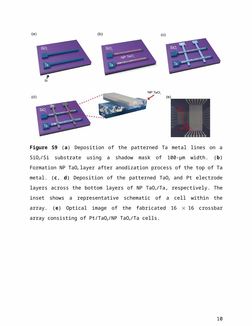
Figure S10 and Table S1 show the fitting results of analog conductance changes (G = PSC/Vr)
for LTP and LTD according to the potentiating and the depressing input-signal trains based on
Figure 2h, respectively. Because the experimental G value of the artificial synapse determines
the degree of the update of synaptic weight, we fitted each G value for LTP and LTD using the
following equations (Figures 2h and S10);S2,S3
∆ Gp=ap+b p e−cp
G−Gmin
Gmax−Gmin (1)
∆ Gd=ad+bd e−cd
Gmax−GGmax−Gmin (2)
Where ΔGp and ΔGd represent the conductance changes for LTP and LTD, respectively; ap, bp, cp,
ad, bd, and cd are the fitting parameters for ΔGp and ΔGd; and the subscripts p and d denote
potentiation and depression, respectively. Note that the only present conductance state (G)
determines subsequent ΔGp and ΔGd values. The value of w is constrained by the range of the
experimental ΔG values of the TaOy/NP TaOx memristor synapse. This simulation based on ΔGp
and ΔGd enables us to evaluate the learning capability of the ANNs consisting of artificial
synapses when S.C = 0. The fitting parameters for 40 ms are presented in Table S1. Based on
these parameters, we constructed a simulation of the MNIST pattern recognition method.
10

Flow chart of the learning process
Figure S11. Details of the flow chart for one epoch of the learning process.
11

Figure S11 illustrates the details of the flow chart for one epoch of the learning process. First, we
initialize all conductances (G+ and G-) to a random distribution between Gmax and Gmin in the
array; then, 60,000 training images (n = 1, 2, ..., 60,000) are fed to the ANNs. Then, the input at
ith is scaled by its own conductance (Gi,j+ × xi
n and Gi,j- × xi
n) and all scaled inputs are transmitted
to the jth output neuron in the form of ∑wi,jxi = ∑Gi,j+xi - ∑Gi,j
-xi.S4,S5 Note that we assume that
IUndesired = ION S.C, which can be inevitably generated from each individual synapse for
simplicity. Eventually, this process can increase the final transmitted value (∑wi,jxi + ∑IUndesired) at
the jth output neuron. Next, the output values (y) are calculated using the sigmoid activation
function f(∑wi,jxi + ∑IUndesired) and the old weights (wold) are updated using the delta rule algorithm
(Δwi,j = ηejxi, where η = 0.005 and ej = tj – yj).S6 When all 60,000 training images are fed into the
network, the next epoch begins. In the case of S.C = 1, all weights (wi,j Gi,j+
- Gi,j-) converge to
approximately zero (Figure 4c), because all memristor synapses generate the highest PSC value
based on IUndesired. Therefore, higher S.C values naturally cause degradation of the accuracy of
pattern recognition. However, in the case of S.C = 0, IUndesired does not influence the weighted sum
(∑wixi) because of full deactivation of undesired pathways, which leads to an ideal weight update
such as in software-based learning.
12

Figure S12. Reconfigured LTP and LTD curves. The linearity in weight update is estimated to
~0.75. The dynamic range is ~55.
The linearity in the weight update can be calculated by the following equationS3,
Linearity∈weight update=maxGp(n)−Gd (n)
Gmax−Gmin
, n = 1 - 100
where G(n) represents the conductance value after the nth programming pulse; subscripts p and d
denote potentiation and depression, respectively; Gmax and Gmin indicate maximum conductance
and minimum conductance, respectively; and the denominator is for normalization. Note that this
value ranges from 0 to 1, and should be zero for a perfectly linear weight update. From this
equation, the linearity in the weight update for our memristive synapse is found to be ~0.75.
13

Figure S13. (a) Standard deviation of the LTP/LTD change at every input pulse from Figure 2h.
(b) The difference in the recognition accuracies between two cases; (i) the variation factor is
considered, and (ii) it is not considered. Note that we assumed that this deviation complies with a
normal distribution in the simulation.
References
S1 Wang, G., Lauchner, A. C., Lin, J., Natelson, D., Palem, K. V. & Tour, J. M. High‐
Performance and Low‐Power Rewritable SiOx 1 kbit One Diode–One Resistor Crossbar
Memory Array. Adv. Mater. 25, 4789-4793 (2013).
S2 Querlioz, D., Bichler, O. & Gamrat, C. Simulation of a memristor-based spiking neural
network immune to device variations. Presented at the 2011 International Joint
Conference on Neural Networks, San Jose, July 31-August 5, 2011.
S3 Kim, S., Choi, B., Lim, M., Yoon, J., Lee, J., Kim, H.-D. & Choi, S.-J. Pattern
recognition using carbon nanotube synaptic transistors with an adjustable weight update
protocol. ACS nano 11, 2814-2822 (2017).
S4 Zidan, M. A., Strachan, J. P. & Lu, W. D. The future of electronics based on memristive
systems. Nat. Electron. 1, 22 (2018).
S5 Zamanidoost, E.; Bayat, F. M.; Strukov, D.; Kataeva, I. Manhattan rule training for
memristive crossbar circuit pattern classifiers. Presented at the 2015 IEEE 9th
International Symposium on Intelligent Signal Processing, Siena, 15-17, May, 2015.
14

S6 Rumelhart, D. E., Hinton, G. E., & Williams, R. J. In Parallel distributed processing (ed.
Rumelhart, D. E., McClelland, J. L.) Ch.8, 318-363 (MIT Press, Cambridge,
Massachusetts, USA, 1985).
15